design type iii compensation network for voltage mode step
TRANSCRIPT

1
APPLICATION NOTE
Design Type III Compensation Network For Voltage Mode Step-down Converters
Skyworks Solutions, Inc. • Phone [781] 376-3000 • Fax [781] 376-3100 • [email protected] • www.skyworksinc.com 202376A • Skyworks Proprietary Information • Products and Product Information are Subject to Change Without Notice. • September 21, 2012
IntroductionThis application note details how to calculate a type III compensation network and investigates the relationship between phase margin and load transient response for the Skyworks family of voltage mode control step-down converters. This family includes the AAT1184, AAT1185, AAT1189, AAT2687, AAT2688, and AAT2689. Voltage mode control has become a very popular topology for DC to DC converters, especially with low noise output systems including DSL and cable modems, notebook computers, satellite set-top boxes, and wireless LAN systems.
BackgroundIn order to reduce the DC-DC converter’s output voltage ripple, the equivalent series resistance (ESR) of the output capacitor needs to be reduced. Ceramic output capacitors have a very small equivalent series resistance (ESR), low cost, and small size, making them the ideal output filter solution for DC-to-DC converters. However, the use of low ESR ceramic capacitors significantly affects the design of the error amplifier in the feedback loop. The power stage consists of a double pole due to the L COUT filter and an ESR zero. The ESR zero is pushed far away from the double pole fre-quency which results in inadequate phase margin at the cross-over frequency. Therefore, type III compensation is used to stabilize the loop and optimize the output transient response to dynamic load changes.
Voltage Mode Control LoopAs illustrated in Figure 1, a typical voltage mode control loop has three main stages: step-down power stage, compen-sation network, and PWM modulator. The Type III compensation network generates two zeros and two poles. The two zeros are placed from 60% to 150% of double pole frequency to counter the 180° phase lag due to the L COUT output filter. The two poles are set at the switching frequency of the converter to nullify the ESR zero and attenuate the high frequency noise.
RDCR
C1
C2
R1
COUT
L
Rfbh
Rfbl
Cff RffCOMPARATOR
Error Amp
RESRROUT
VOUT
Vreff
VIN
Driver
RAMP
PWM MODULATOR
COMP
COMPENSATION NETWORK
STEP-DOWN POWER STAGE
Figure 1: Closed Loop Step-Down Converter with Type III Network Compensation.
DISCON
TINU
ED

2
APPLICATION NOTE
Design Type III Compensation Network For Voltage Mode Step-down Converters
Skyworks Solutions, Inc. • Phone [781] 376-3000 • Fax [781] 376-3100 • [email protected] • www.skyworksinc.com 202376A • Skyworks Proprietary Information • Products and Product Information are Subject to Change Without Notice. • September 21, 2012
Step-Down Power Stage Transfer FunctionThe transfer function of the power stage of the step-down converter can be determined by the voltage division:
Eq. 1: VOUT
VIN
ZOUT
ZL + ZOUT=
Where ZL and ZOUT are the inductor impedance and output impedance of the power stage. The RDCR includes the DC winding resistance, the turn-on resistance of the MOSFET, and the trace resistance. RESR is the equivalent series resis-tor of the output capacitor. ZL and ZOUT are calculated using Equations 2 and 3.
Eq. 2: 1sCOUT
s · COUT · RLOAD · RESR + RLOAD
s · COUT · (RLOAD + RESR) + 1ZOUT = RLOAD // RESR + =
Eq. 3: ZL = s · L + RDCR
Where the complex variable s = j · w and -1j =
RDCR
COUT
L
RESRRLOAD
VOUT
VIN
Driver
STEP-DOWN POWER STAGEZL
ZOUT
Figure 2: Step-Down Converter Power Stage.
The step-down power stage open loop gain is given by substituting Equations 2 and 3 into Equation 1. Algebraic manipulation yields the following expression for the open-loop transfer function of the power stage:
Eq. 4: VOUT
VIN
RLOAD · (s · COUT · RESR + 1)s2 · L · COUT · (RLOAD + RESR) + sL + COUT · [RDCR(RLOAD + RESR) + RLOAD · RESR ] + RLOAD + RDCR
GP = =
A typical Bode plot of the step-down converter power stage is illustrated in Figure 3. A double pole at the cut-off fre-quency causes the gain to roll off with a -40dB/decade slope (blue) and the phase to exhibit a very sharp slope down-ward from 0 degree to -180 degree phase lag (red). The ESR zero is observed at a very high frequency due to the ceramic output capacitor.
DISCON
TINU
ED

3
APPLICATION NOTE
Design Type III Compensation Network For Voltage Mode Step-down Converters
Skyworks Solutions, Inc. • Phone [781] 376-3000 • Fax [781] 376-3100 • [email protected] • www.skyworksinc.com 202376A • Skyworks Proprietary Information • Products and Product Information are Subject to Change Without Notice. • September 21, 2012
Output Double Pole at cut -off frequency
ESR zero at very high frequency
-40dB/dec
-20dB/dec
Frequency (Hz)
Gai
n (d
B)a
nd P
hase
(deg
ree)
-180 degree phase lag due to double pole
Figure 3: The Bode Plot of the Output Stage.
Error Amplifier Transfer Function CalculationThe error amplifier transfer function with type III compensation as shown in Figure 4 is calculated from Equation 5:
Eq. 5: VCOMP
VOUTGE =
1s · C2
1s · C1
// R1 + =
1s · Cff
Rfbh // Rff +
C1R1
C2
Rfbh
Rfbl
Cff Rff
Error Amp
VREFVCOMP
VOUT
Z2
Z1
P2
P1
Figure 4: Error Amplifier With Type III Compensation Network.
DISCON
TINU
ED

4
APPLICATION NOTE
Design Type III Compensation Network For Voltage Mode Step-down Converters
Skyworks Solutions, Inc. • Phone [781] 376-3000 • Fax [781] 376-3100 • [email protected] • www.skyworksinc.com 202376A • Skyworks Proprietary Information • Products and Product Information are Subject to Change Without Notice. • September 21, 2012
By algebraic manipulation, GE can be explicitly expressed in terms of zeros and poles in Equation 6.
Eq. 6: Rfbh + Rff
Rfbh · Rff · C2GE =
1R1 · C1
1(Rfbh + Rff) · Cff
· s + s + ·
(C1 + C2)R1 · C1 · C2
1Rff · Cff
s · s + · s +
Equation 6 gives two zeroes at frequencies FZ1 and FZ2 and two poles at frequencies FP1 and FP2 in the following expres-sions:
12π · (Rfbh + Rff) · Cff
FZ1 = 12π · R1 · C1
FZ2 = and
1and FP2 = 12π · Rff · Cff
FP1 = C1 · C2
C1 + C22π · R1 ·
Gai
n (d
B)an
d Ph
ase
(deg
ree)
180 degree phase boost
Placing the two poles at cross -over frequency
Placing the two zeros close to the output double pole
frequency
Figure 5: Error Amplifier With Type III Compensation Bode Plot.
Type III compensation provides two zeros and two poles which push the cross-over frequency as high as possible and boosts the phase margin greater than 45 degree. A higher bandwidth yields a faster load transient response. The faster transient response results in a smaller output voltage spike.
PWM Modulator StageThe PWM modulator gain is inversely proportional to the peak-to-peak input ramp voltage of the oscillator and is derived via Equation 7.
Eq. 7: VIN
VRAMPGM =
DISCON
TINU
ED

5
APPLICATION NOTE
Design Type III Compensation Network For Voltage Mode Step-down Converters
Skyworks Solutions, Inc. • Phone [781] 376-3000 • Fax [781] 376-3100 • [email protected] • www.skyworksinc.com 202376A • Skyworks Proprietary Information • Products and Product Information are Subject to Change Without Notice. • September 21, 2012
Step-Down Converter Loop Gain with Type III CompensationThe loop gain of the system is expressed in terms of GM, GE, and GP factors as shown in Equation 8.
Eq. 8: GLOOP = GM · GE · GP
The magnitude in dB and the phase in degree of the converter loop gain are derived from Equations 9 and 10.
Eq. 9: GLOOP (dB) = 20.log (GLOOP) = 20.log (GM · GE · GP)
Eq. 10: 180π
PLOOP = arg(GLOOP) ·
The magnitude and phase Bode plots of the converter loop gain with type III compensation are shown in Figure 5. By placing the two zeros close to the output double pole and the two poles at switching frequency, the crossover fre-quency is pushed to 10% to 60% of switching frequency and in the vicinity of maximum phase boost in order to achieve an optimum phase margin ΦM.
ΦM
Output Double Pole
Placing the two zeros close to the output double pole
frequency
Gai
n (d
B)an
d Ph
ase
(deg
ree)
Cross-Over Frequency at 1/10
Switching Frequency
Figure 6: Step-Down Converter Loop Gain With Type III Compensation Bode Plot .DISCON
TINU
ED

6
APPLICATION NOTE
Design Type III Compensation Network For Voltage Mode Step-down Converters
Skyworks Solutions, Inc. • Phone [781] 376-3000 • Fax [781] 376-3100 • [email protected] • www.skyworksinc.com 202376A • Skyworks Proprietary Information • Products and Product Information are Subject to Change Without Notice. • September 21, 2012
Type III Compensation Design Process For Voltage Mode Control Step-Down Converter:For example, assume the voltage mode step-down converter has the following specifications:
VIN = 6V to 24VVOUT = 3.3V
VOUT - VREF
VREF
3.3V - 0.6V0.6V
RFBL = 6.04KΩ, RFBH = RFBL · = 6.04K · = 27.4KΩ
VIN
12VRAMP =
L = 4.7µHCOUT = 2x22µF, ESR = 2mΩIOUT = 2.5AFSW = 490KHz
1. Set the crossover frequency in the range of 1/6 to 1/10 of switching frequency to avoid the Niquist pole:
Eq. 11: FSW
10FC = = 49KHz
2. Place the first zero from 60% to 150% of the double pole frequency of the L COUT filter:
Eq. 12: L · COUT
K · Rfbh= = 481pFCff =
4.7µH · 44µF 1.1 · 27.4KΩ
Where the value of factor K is within the range of 0.6 to 1.5.
3. Set the first pole at switching frequency and calculate Rff from:
Eq. 13: 1
2π · Cff · FSW
12π · 481pF · 490KHz
Rff = = = 675Ω
4. At cross-over frequency (FC) the loop gain is unity. Setting |GLOOP|= 1 at s = jwc, the value of R1 is given by Equation 14.
Eq. 14: (2π · FC)2 · L · COUT + 1
2π · FC · Cff
(2π · 49KHz)2 · 4.7µH · 44µF2π · 49KHz · 481pF
VRAMP
VINR1 = · = = 11.6KΩ
5. Set the second zero to coincide with the first zero, and solve for C1:
Eq. 15: L · COUT
K · R1= = 112pFC1 =
4.7µH · 44µF 1.1 · 11.6KΩ
6. Place the second pole from switching frequency to one decay higher for adequate phase margin, and solve for C2:
Eq. 16: 1
2π · R1 · FSW
12π · 11.6KΩ · 490KHz
C2 = = = 28pF
DISCON
TINU
ED

7
APPLICATION NOTE
Design Type III Compensation Network For Voltage Mode Step-down Converters
Skyworks Solutions, Inc. • Phone [781] 376-3000 • Fax [781] 376-3100 • [email protected] • www.skyworksinc.com 202376A • Skyworks Proprietary Information • Products and Product Information are Subject to Change Without Notice. • September 21, 2012
The Relationship between Frequency Domain and Time Domain in a Step-Down ConverterKnowing the relationship between the phase margin in the frequency domain and load transient response in time domain is beneficial to achieving the best results. In this way, we can select either a slow output transient response but without any overshoot or, a faster output transient response with a small amount of overshoot. Let’s concentrate on the small area in the vicinity of the cross over frequency (see Figure 7). The curve has two different slopes (-20dB/decade and -40dB/ decade) due to the location of the original pole w0 and the high frequency pole w2. Assuming the other compensation pole w1 and the ESR zero are cancelled out. The open loop transfer function in this region can be approximated by Equation 17:
Eq. 17: T(s) ≈ 1
1 +sω0
sω2
The close loop transfer function can derive from T(s):
Eq. 18: 11 + T(s)
GLOOP (s) = +
= 1s2
ω0 · ω2+ 1
sω0
+= 1
s2
ωr2
sωr · Q
+ 1
Where the quality coefficient Q and the resonant frequency wr are defined using Equations 19 and 20.
Eq. 19: ω0
ω2Q =
Eq. 20: ω0ω2ωr =
The cross-over frequency wc can be solved by equating Equation 18 to unity at the crossover frequency:
Eq. 21:
ω0
ω2
21 + 4 - 1
2ωc = ω2 = ω2
21 + 4(Q) - 1
2
ΦM
Output Double Pole
Placing the two zeros close to the output double pole
frequency
Gai
n (d
B)an
d Ph
ase
(deg
ree)
Cross-Over Frequency at 1/10
Switching Frequency
Figure 7: The Gain Curve Has Two Different Slopes (-20dB/decade and -40dB/decade) at Crossover Frequency due to the Location of the Original Pole ω0 and the High Frequency Pole ω2.
DISCON
TINU
ED

8
APPLICATION NOTE
Design Type III Compensation Network For Voltage Mode Step-down Converters
Skyworks Solutions, Inc. • Phone [781] 376-3000 • Fax [781] 376-3100 • [email protected] • www.skyworksinc.com 202376A • Skyworks Proprietary Information • Products and Product Information are Subject to Change Without Notice. • September 21, 2012
Eq. 22:
ωC
ω0
0ωC
ω2
ωC
ω2
π2
-1 -1-1arg T(ωC) = - tan + tan = -tan -
Eq. 23: ω2
ωC
21 + 4Q4 - 1
-1 -1ϕM = π + arg T(ωC) = tan = tan
The relationship between the phase margin and the quality coefficient can be derived from Equation 23:
Eq. 24: Q = = 1 + tan(ϕM)2
tan(ϕM)
cos(ϕM)
sin(ϕM)
The percent overshoot and quality factor in the second order system are given by Equation 25.
Eq. 25: %OS = 100 · e = 100 · e-π
4Q2 - 1 - 1
-π4cosϕM
sin2ϕM
Figure 8 plots the percent overshoot versus phase margin of a typical second order system.
Percent Overshoot vs. Phase Margin
0
10
20
30
40
50
60
70
80
0 10 20 30 40 50 60 70 80
Phase Margin (degree)
Pece
nt O
vers
hoot
(%)
Figure 8: Percent Overshoot vs. Phase Margin for Second Order System.
The output transient response of a 3.3V output step-down converter with different phase margin is measured in Figure 9. The step load is generated from 200mA to 2.5A with 2A/µs slew rate. The red curve corresponding to 68° phase margin has 160µs recovery time without overshoot and a transient voltage spike of 404mV. The black and green curves experience very fast recovery time (40µs) with very small overshoot and a small transient voltage spike of 280mV. Finally, the blue and pink curves reveal an unstable system due to the phase margin of less than 45°.
DISCON
TINU
ED

9
APPLICATION NOTE
Design Type III Compensation Network For Voltage Mode Step-down Converters
Skyworks Solutions, Inc. • Phone [781] 376-3000 • Fax [781] 376-3100 • [email protected] • www.skyworksinc.com 202376A • Skyworks Proprietary Information • Products and Product Information are Subject to Change Without Notice. • September 21, 2012
3.3V
3.4V
3.5V
3.6V
3.2V
3.1V
3.0VTime (40µs/div)
Out
put V
olta
ge (1
00m
V/div)
PM=68º
PM=26ºPM=33ºPM=48ºPM=58º
Figure 9: The Relationship Between Phase Margin, Overshoot and Recovery Time of the Output Transient Response of a 3.3V Output Buck Converter.
Phase Margin and Transient Response vs. DC Gain (FC = 50KHz)Based on the discussion above of the frequency domain and time domain, the recovery time can be adjusted faster to reduce the peak-to-peak output transient response of a step-down converter. This can be done by pushing the zeros a bit above the double poles frequency (K = 1.1) in order to boost the DC gain from 65dB to 75dB. Figure 10 illustrates the relationship between the phase margin and load transient response for K = 0.6 and K = 1.1 at the same crossover frequency of 50KHz. A higher DC gain along with a smaller phase margin of 58° yields a faster recovery time of 60µs, which results in a smaller peak-to-peak output transient response (280mV) for a 200mA to 2.5A dynamic load.
PM=68º
PM=58º
K=0.6
K=1.1
Fco =50KHz
Fco =50KHz
VPP =404mV
VPP =280mV
Frequency (Hz)
Frequency (Hz)
Time (40μs/div)
Time (40μs/div)
Frequency Domain Time Domain
2.5A
200mA
2.5A
200mA
tr=60us
tr=140us
DC Gain = 65dB
DC Gain = 75dB Cff = 470pF Rff = 681Ω
R1 = 11.5kΩC1 = 1nF
C2 = 27pF
Cff = 1nF Rff = 365Ω
R1 = 3.34kΩ C1 = 3300pF
C2 = 47pF
Figure 10: Phase Margin and Transient Response For Differing K Factors (K = 0.6 and K = 1.1).
DISCON
TINU
ED

10
APPLICATION NOTE
Design Type III Compensation Network For Voltage Mode Step-down Converters
Skyworks Solutions, Inc. • Phone [781] 376-3000 • Fax [781] 376-3100 • [email protected] • www.skyworksinc.com 202376A • Skyworks Proprietary Information • Products and Product Information are Subject to Change Without Notice. • September 21, 2012
Phase Margin and Transient Response vs. Bandwidth (K = 1.1)As illustrated in Figure 11, the output voltage spike can be further improved by pushing the crossover frequency (FC) to 80KHz if a small amount of overshoot is acceptable. However, further increasing the bandwidth reduces the phase margin below 45°, resulting in an unstable system. In addition, increasing the bandwidth to exceed the effective control bandwidth no longer reduces the output voltage spike due to the voltage drop across the ESR of the output capacitor which dominates the transient voltage spike.
For a 3.3V output voltage buck converter using a 4.7µH inductor during a load transient step from 200mA to 2.5A, the effective control bandwidth is derived from Equation 26.
Eq. 26: VO
4 · ∆IO · L3.3V
4 · 2.5A · 4.7µH= = 76KHzFCE =
PM=58º
PM=55º
K=1.1
K=1.1
K=1.1
K=1.1
Fco =50KHz
Fco =80KHz
VPP =280mV
VPP = 266mV
Frequency Domain
Frequency (Hz)
Frequency (Hz)
Time (40μs/div)
Time (40μs/div)
Time Domain
200mA
2.5A
2.5A
200mA
Cff = 470pF Rff = 681Ω
R1 = 18.7kΩ C1 = 680pF C2 = 18pF
Cff = 470pF Rff = 681Ω
R1 = 11.5kΩC1 = 1nF
C2 = 27pF
Figure 11: Frequency Domain vs. Time Domain For Different Bandwidth (FCO = 50KHz and FCO = 80KHz).
DISCON
TINU
ED
11
APPLICATION NOTE
Design Type III Compensation Network For Voltage Mode Step-down Converters
Skyworks Solutions, Inc. • Phone [781] 376-3000 • Fax [781] 376-3100 • [email protected] • www.skyworksinc.com 202376A • Skyworks Proprietary Information • Products and Product Information are Subject to Change Without Notice. • September 21, 2012
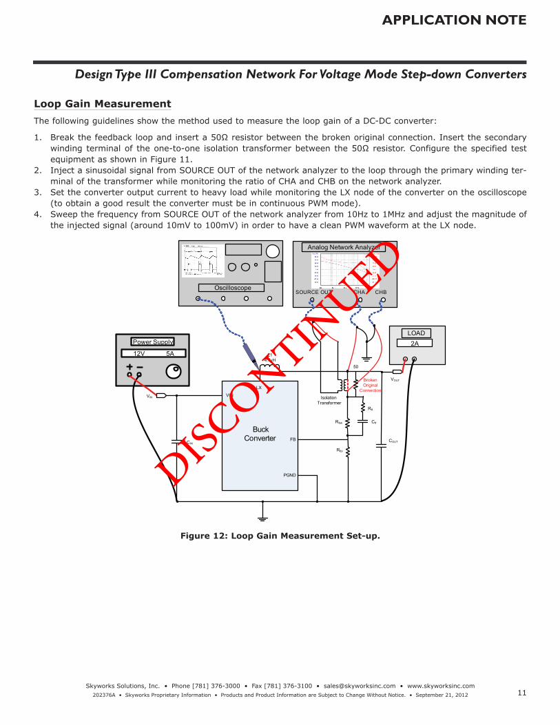
Loop Gain MeasurementThe following guidelines show the method used to measure the loop gain of a DC-DC converter:
1. Breakthefeedbackloopandinserta50Ωresistorbetweenthebrokenoriginalconnection.Insertthesecondarywinding terminalof theone-to-one isolation transformerbetweenthe50Ωresistor.Configure thespecified testequipment as shown in Figure 11.
2. Inject a sinusoidal signal from SOURCE OUT of the network analyzer to the loop through the primary winding ter-minal of the transformer while monitoring the ratio of CHA and CHB on the network analyzer.
3. Set the converter output current to heavy load while monitoring the LX node of the converter on the oscilloscope (to obtain a good result the converter must be in continuous PWM mode).
4. Sweep the frequency from SOURCE OUT of the network analyzer from 10Hz to 1MHz and adjust the magnitude of the injected signal (around 10mV to 100mV) in order to have a clean PWM waveform at the LX node.
Oscilloscope
LOAD2A
12V 5A
Power Supply
Analog Network Analyzer
SOURCE OUT CHA CHB
VOUT
VIN
LX
Rff
Cff
Buck Converter
VIN
FB COUT
Rfbh
Rfbl
PGND
L14.7µH
50
Isolation Transformer
Broken Original
Connection
CIN
Figure 12: Loop Gain Measurement Set-up.
DISCON
TINU
ED

12
APPLICATION NOTE
Design Type III Compensation Network For Voltage Mode Step-down Converters
Skyworks Solutions, Inc. • Phone [781] 376-3000 • Fax [781] 376-3100 • [email protected] • www.skyworksinc.com 202376A • Skyworks Proprietary Information • Products and Product Information are Subject to Change Without Notice. • September 21, 2012
Copyright © 2012 Skyworks Solutions, Inc. All Rights Reserved.
Information in this document is provided in connection with Skyworks Solutions, Inc. (“Skyworks”) products or services. These materials, including the information contained herein, are provided by Skyworks as a service to its customers and may be used for informational purposes only by the customer. Skyworks assumes no responsibility for errors or omissions in these materials or the information contained herein. Sky-works may change its documentation, products, services, specifications or product descriptions at any time, without notice. Skyworks makes no commitment to update the materials or information and shall have no responsibility whatsoever for conflicts, incompatibilities, or other difficulties arising from any future changes.
No license, whether express, implied, by estoppel or otherwise, is granted to any intellectual property rights by this document. Skyworks assumes no liability for any materials, products or information provided here-under, including the sale, distribution, reproduction or use of Skyworks products, information or materials, except as may be provided in Skyworks Terms and Conditions of Sale.
THE MATERIALS, PRODUCTS AND INFORMATION ARE PROVIDED “AS IS” WITHOUT WARRANTY OF ANY KIND, WHETHER EXPRESS, IMPLIED, STATUTORY, OR OTHERWISE, INCLUDING FITNESS FOR A PARTICULAR PURPOSE OR USE, MERCHANTABILITY, PERFORMANCE, QUALITY OR NON-INFRINGEMENT OF ANY INTELLECTUAL PROPERTY RIGHT; ALL SUCH WARRANTIES ARE HEREBY EXPRESSLY DISCLAIMED. SKYWORKS DOES NOT WARRANT THE ACCURACY OR COMPLETENESS OF THE INFORMATION, TEXT, GRAPHICS OR OTHER ITEMS CONTAINED WITHIN THESE MATERIALS. SKYWORKS SHALL NOT BE LIABLE FOR ANY DAMAGES, IN-CLUDING BUT NOT LIMITED TO ANY SPECIAL, INDIRECT, INCIDENTAL, STATUTORY, OR CONSEQUENTIAL DAMAGES, INCLUDING WITHOUT LIMITATION, LOST REVENUES OR LOST PROFITS THAT MAY RESULT FROM THE USE OF THE MATERIALS OR INFORMATION, WHETHER OR NOT THE RECIPIENT OF MATERIALS HAS BEEN ADVISED OF THE POSSIBILITY OF SUCH DAMAGE.
Skyworks products are not intended for use in medical, lifesaving or life-sustaining applications, or other equipment in which the failure of the Skyworks products could lead to personal injury, death, physical or en-vironmental damage. Skyworks customers using or selling Skyworks products for use in such applications do so at their own risk and agree to fully indemnify Skyworks for any damages resulting from such improper use or sale.
Customers are responsible for their products and applications using Skyworks products, which may deviate from published specifications as a result of design defects, errors, or operation of products outside of pub-lished parameters or design specifications. Customers should include design and operating safeguards to minimize these and other risks. Skyworks assumes no liability for applications assistance, customer product design, or damage to any equipment resulting from the use of Skyworks products outside of stated published specifications or parameters.
Skyworks, the Skyworks symbol, and “Breakthrough Simplicity” are trademarks or registered trademarks of Skyworks Solutions, Inc., in the United States and other countries. Third-party brands and names are for identification purposes only, and are the property of their respective owners. Additional information, including relevant terms and conditions, posted at www.skyworksinc.com, are incorporated by reference.
ConclusionUsing low ESR ceramic output capacitors for voltage mode controlled buck converters yields very low output voltage ripple, but requires type III compensation for adequate phase margin. The type III compensation network provides two zeros and two poles that push the crossover frequency to a possible maximum value with adequate phase margin for the control loop. The trade-off between the stability and output transient response can be adjusted by using the factor K, which represents the position of zeros in the vicinity frequency of the output double poles. In applications which require no overshoot, the two zeros are placed at 60% (K = 0.6) of the output double poles frequency to achieve approximately 70 degrees of phase margin. However, if the transient output voltage spike is critical, the two zeros can be placed up to 150% (K = 1.5) of the output double pole frequency if a small amount of overshoot is acceptable. In addition, a higher bandwidth yields a faster transient response. However, a bandwidth higher than the critical bandwidth can no longer reduce the transient output voltage spike. A typical bandwidth for type III compensation is in the range of 10% to 60% of switching frequency.
DISCON
TINU
ED