design of robust and flexible on-chip analog-to-digital conversion architecture ph. d. dissertation...
TRANSCRIPT
Design of Robust and Flexible On-chip Analog-to-Digital Conversion
Architecture
Ph. D. Dissertation Proposal Presentationof Daeik Kim
Advisor : Prof. Martin Brooke
School of Electrical and Computer EngineeringGeorgia Institute of Technology
2
Overview
• Background• Literature review• Research proposal• Preliminary research• Future research• Conclusion

3
Background• Bio-optoelectronic
sensor system (BOSS)• System-on-chip (SoC)
integration of analog-to-digital converter (ADC) on Si-CMOS circuit
• Research question: How to evaluate, select, and design a flexible and robust ADC system?
• Investigate unified evaluation and design criteria for ADCs
Simplified view of sensor system
4
Literature Review
• Nyquist ADC• Delta-sigma oversampling ADC• Noise characterization• Signal modeling
5
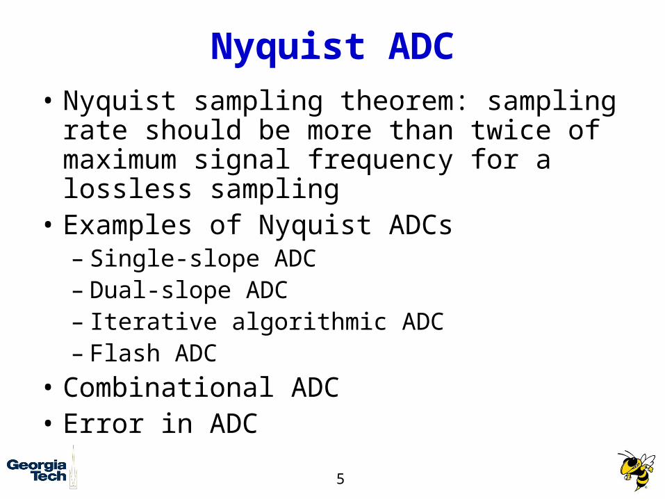
Nyquist ADC• Nyquist sampling theorem: sampling
rate should be more than twice of maximum signal frequency for a lossless sampling
• Examples of Nyquist ADCs– Single-slope ADC– Dual-slope ADC– Iterative algorithmic ADC– Flash ADC
• Combinational ADC• Error in ADC
6
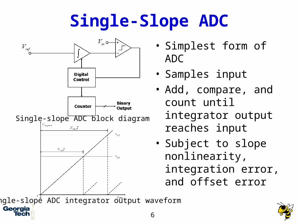
Single-Slope ADC• Simplest form of
ADC• Samples input• Add, compare, and
count until integrator output reaches input
• Subject to slope nonlinearity, integration error, and offset error
Single-slope ADC block diagram
Single-slope ADC integrator output waveform
7
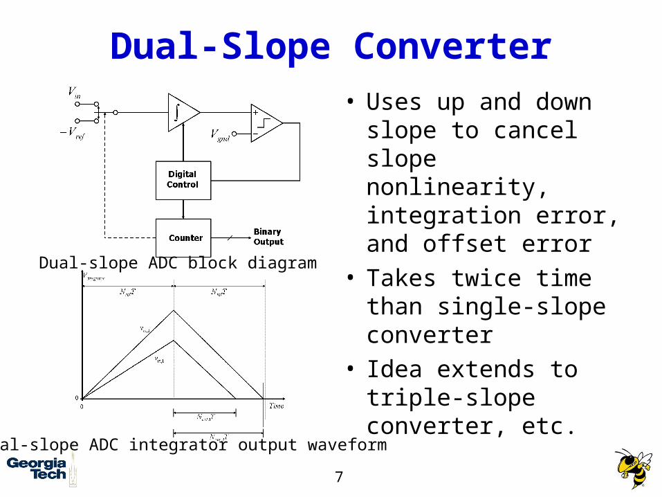
Dual-Slope Converter• Uses up and down
slope to cancel slope nonlinearity, integration error, and offset error
• Takes twice time than single-slope converter
• Idea extends to triple-slope converter, etc.
Dual-slope ADC block diagram
Dual-slope ADC integrator output waveform
8
Iterative Algorithmic Converter
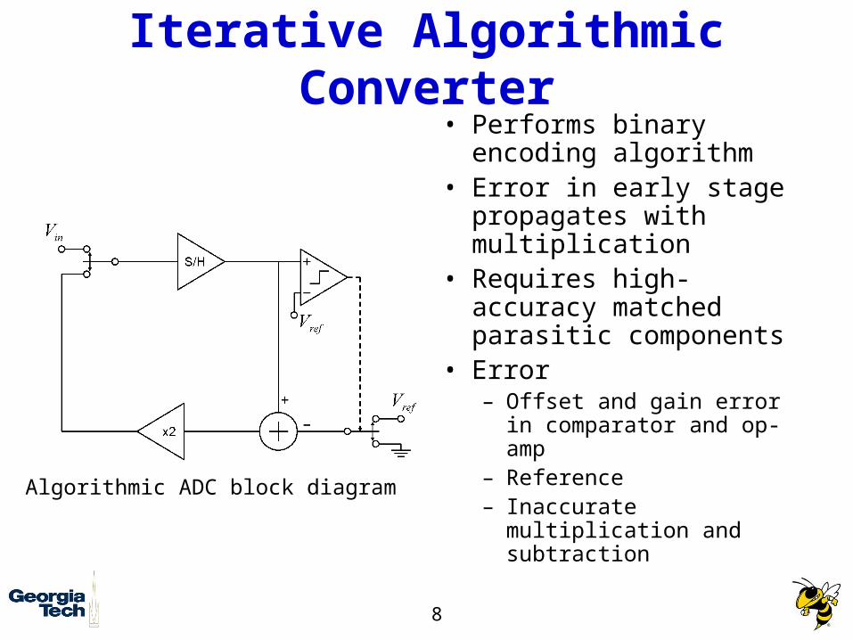
• Performs binary encoding algorithm
• Error in early stage propagates with multiplication
• Requires high-accuracy matched parasitic components
• Error– Offset and gain error in
comparator and op-amp– Reference– Inaccurate
multiplication and subtraction
Algorithmic ADC block diagram
9
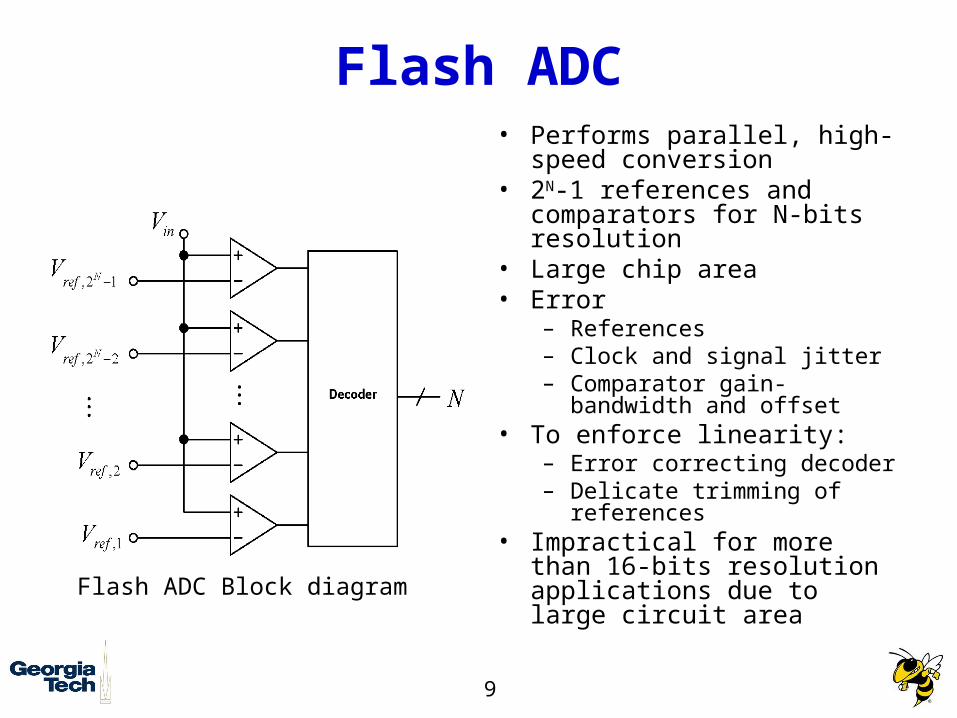
Flash ADC• Performs parallel, high-
speed conversion• 2N-1 references and
comparators for N-bits resolution
• Large chip area• Error
– References– Clock and signal jitter– Comparator gain-
bandwidth and offset• To enforce linearity:
– Error correcting decoder– Delicate trimming of
references• Impractical for more than
16-bits resolution applications due to large circuit area
Flash ADC Block diagram

10
Combinational ADC• Mix of linear, binary, and flash conversion
with time and space multiplexing is used as a trade-off between power, speed, chip area, and resolution
• Examples– Successive approximation ADC– Single-bit iterative pipelined ADC– Multi-bit pipelined ADC– Interpolating ADC– Folding ADC– Time-interleaved ADC
11
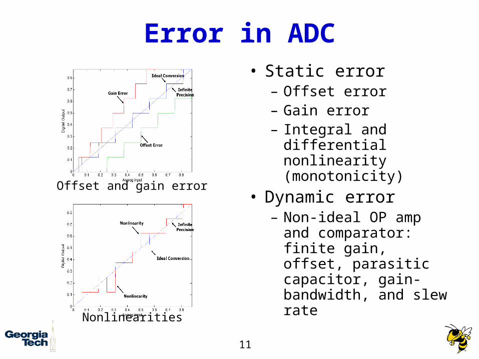
Error in ADC• Static error
– Offset error– Gain error– Integral and
differential nonlinearity (monotonicity)
• Dynamic error– Non-ideal OP amp
and comparator: finite gain, offset, parasitic capacitor, gain-bandwidth, and slew rate
Offset and gain error
Nonlinearities
12
Delta-Sigma Oversampling ADC
• Frequency normalization• Quantization noise• Oversampling• Delta modulation• Noise shaping• Linear analysis• Filtering and downsampling• Issues• Variations
13
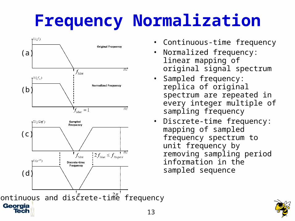
Frequency Normalization• Continuous-time frequency • Normalized frequency:
linear mapping of original signal spectrum
• Sampled frequency: replica of original spectrum are repeated in every integer multiple of sampling frequency
• Discrete-time frequency: mapping of sampled frequency spectrum to unit frequency by removing sampling period information in the sampled sequence
Continuous and discrete-time frequency
(a)
(b)
(c)
(d)
14
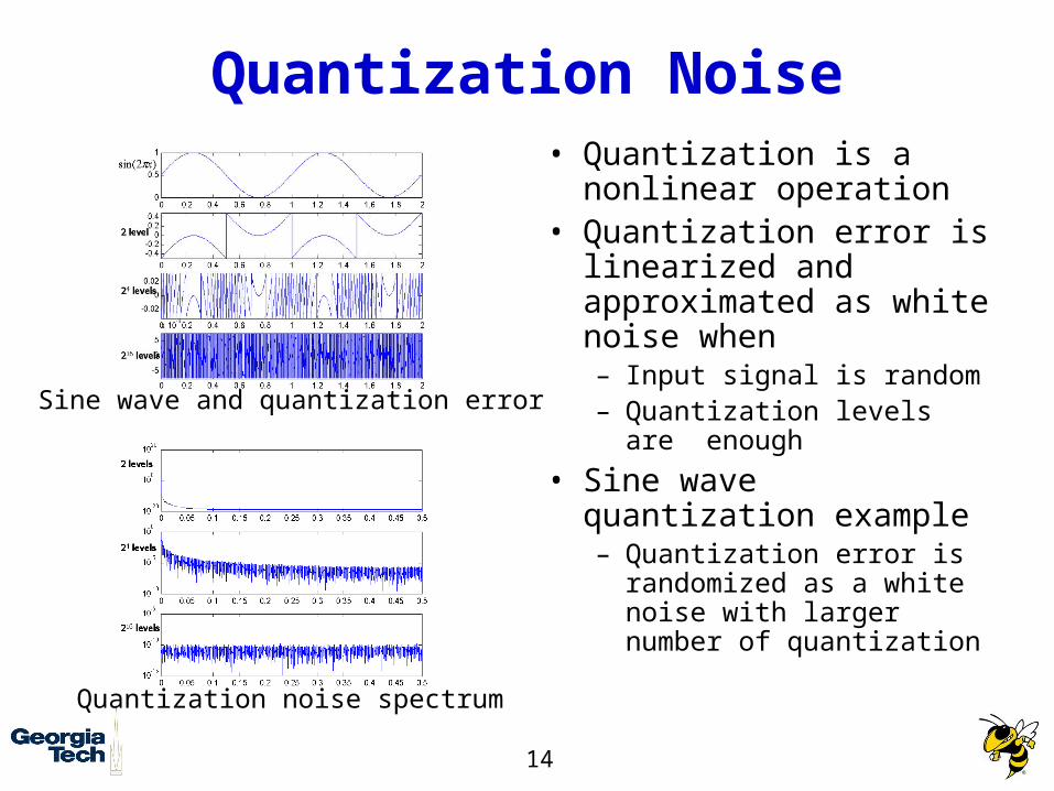
Quantization Noise• Quantization is a
nonlinear operation• Quantization error is
linearized and approximated as white noise when– Input signal is random– Quantization levels are
enough
• Sine wave quantization example– Quantization error is
randomized as a white noise with larger number of quantization
Sine wave and quantization error
Quantization noise spectrum
15
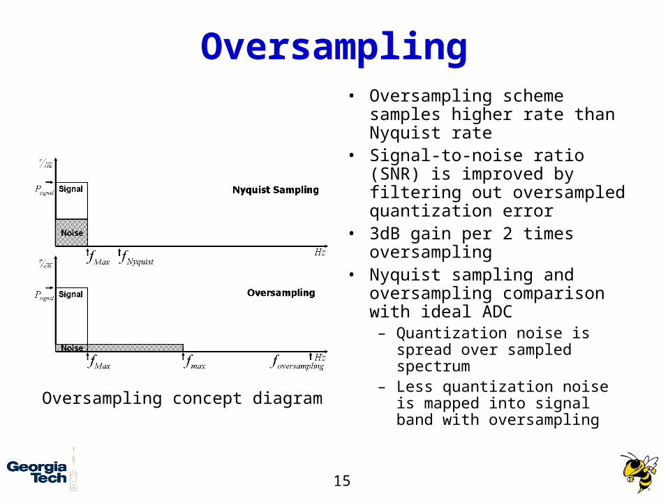
Oversampling• Oversampling scheme
samples higher rate than Nyquist rate
• Signal-to-noise ratio (SNR) is improved by filtering out oversampled quantization error
• 3dB gain per 2 times oversampling
• Nyquist sampling and oversampling comparison with ideal ADC– Quantization noise is
spread over sampled spectrum
– Less quantization noise is mapped into signal band with oversampling
Oversampling concept diagram
16
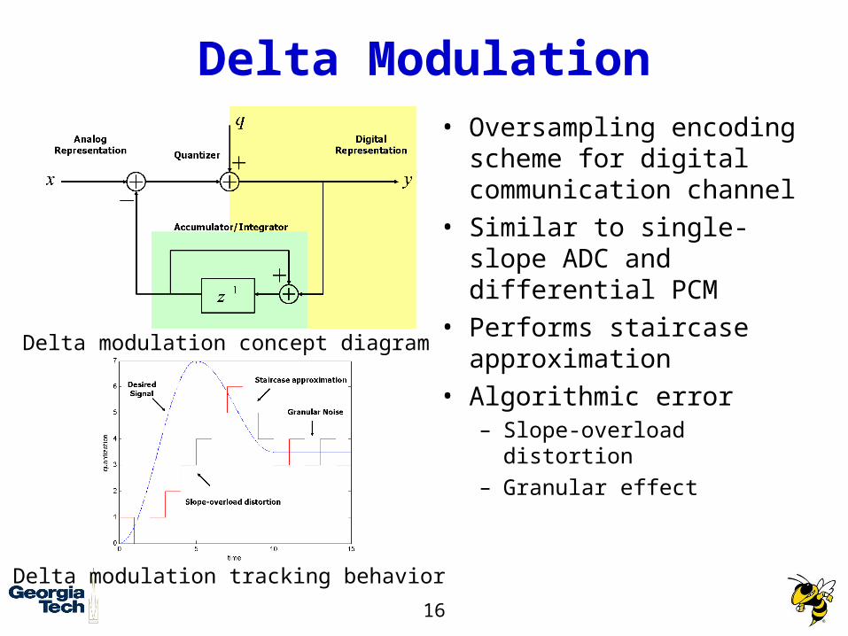
Delta Modulation• Oversampling
encoding scheme for digital communication channel
• Similar to single-slope ADC and differential PCM
• Performs staircase approximation
• Algorithmic error– Slope-overload
distortion– Granular effect
Delta modulation concept diagram
Delta modulation tracking behavior
17
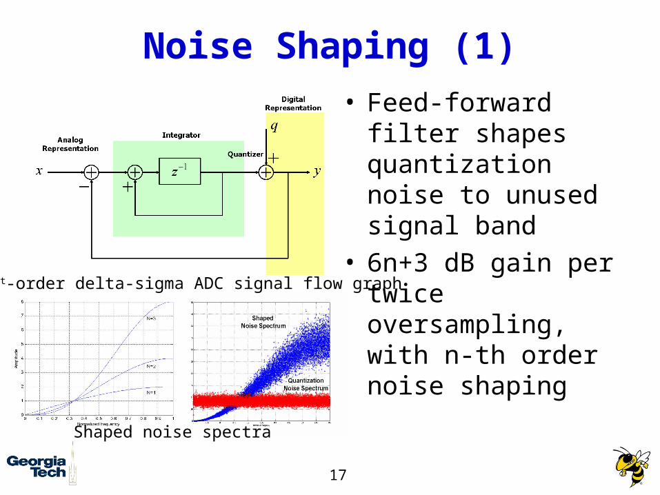
Noise Shaping (1)• Feed-forward filter
shapes quantization noise to unused signal band
• 6n+3 dB gain per twice oversampling, with n-th order noise shaping
1st-order delta-sigma ADC signal flow graph
Shaped noise spectra
18
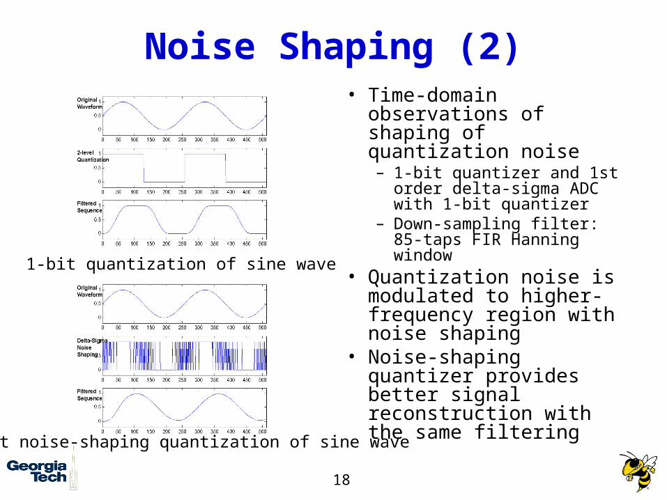
Noise Shaping (2)• Time-domain
observations of shaping of quantization noise– 1-bit quantizer and 1st
order delta-sigma ADC with 1-bit quantizer
– Down-sampling filter: 85-taps FIR Hanning window
• Quantization noise is modulated to higher-frequency region with noise shaping
• Noise-shaping quantizer provides better signal reconstruction with the same filtering
1-bit quantization of sine wave
1-bit noise-shaping quantization of sine wave
19
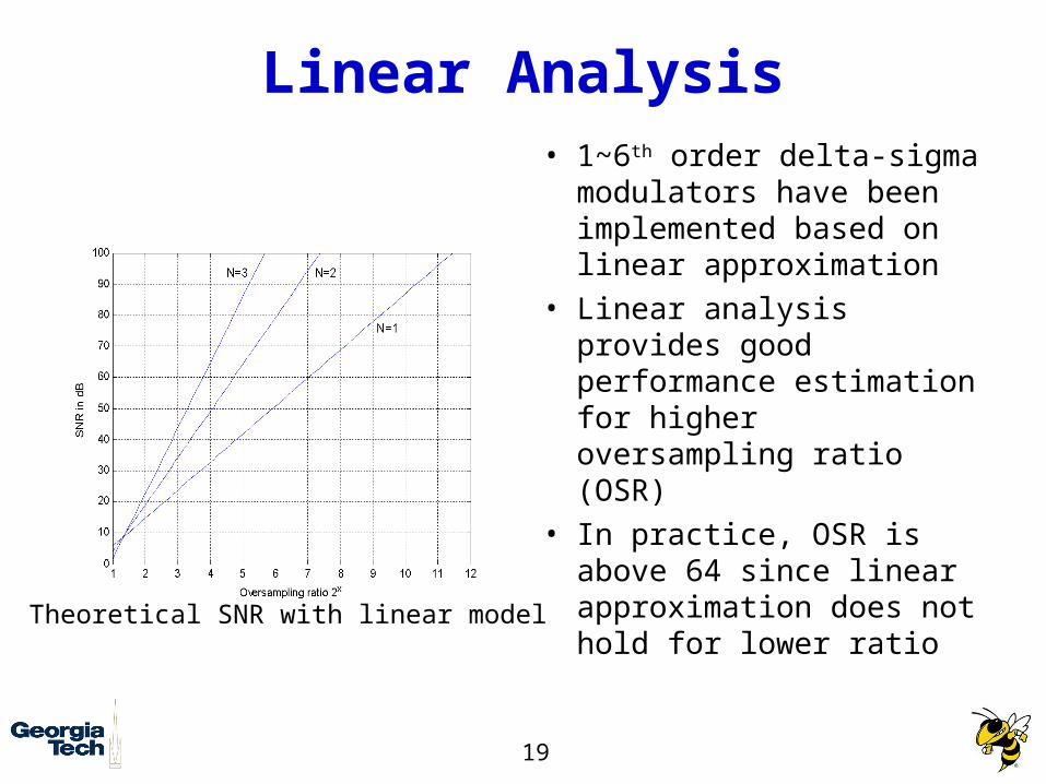
Linear Analysis• 1~6th order delta-sigma
modulators have been implemented based on linear approximation
• Linear analysis provides good performance estimation for higher oversampling ratio (OSR)
• In practice, OSR is above 64 since linear approximation does not hold for lower ratio
Theoretical SNR with linear model
20
Filtering and Downsampling
• Linear filters– Designed in frequency domain with linear approximation– 1~4th order comb (sinc) filters– Various sub-optimal filters
• Nonlinear dc level decoding schemes– Modeling of internal states and observation of time
domain behavior– Cyclic model decoding– Autocorrelation method– Zoomer algorithm– Viterbi decoding
• Nonlinear band-limited signal reconstruction algorithms– Based on projection on convex set (POCS) and singular
value decomposition (SVD)
21
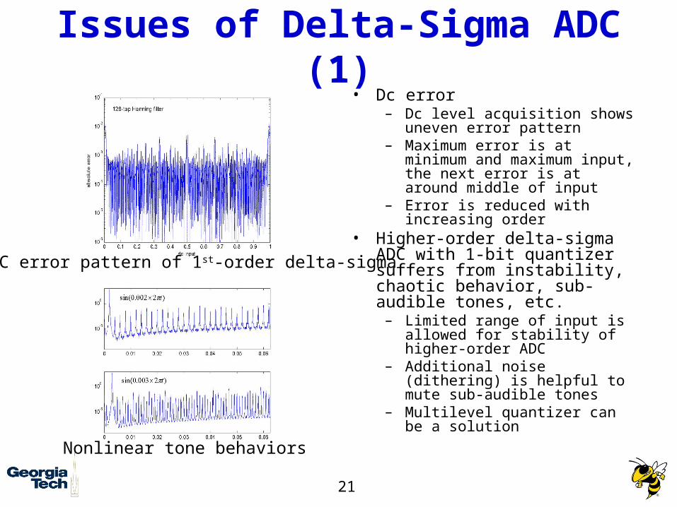
Issues of Delta-Sigma ADC (1)
• Dc error– Dc level acquisition shows
uneven error pattern– Maximum error is at minimum
and maximum input, the next error is at around middle of input
– Error is reduced with increasing order
• Higher-order delta-sigma ADC with 1-bit quantizer suffers from instability, chaotic behavior, sub-audible tones, etc.– Limited range of input is
allowed for stability of higher-order ADC
– Additional noise (dithering) is helpful to mute sub-audible tones
– Multilevel quantizer can be a solution
Nonlinear tone behaviors
DC error pattern of 1st-order delta-sigma
22
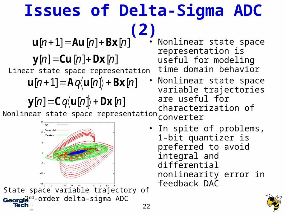
Issues of Delta-Sigma ADC (2)
• Nonlinear state space representation is useful for modeling time domain behavior
• Nonlinear state space variable trajectories are useful for characterization of converter
• In spite of problems, 1-bit quantizer is preferred to avoid integral and differential nonlinearity error in feedback DAC
][][][
][][]1[
nnn
nnn
DxCuy
BxΑuu
Linear state space representation
State space variable trajectory of2nd-order delta-sigma ADC
][][][
][][]1[
nnqn
nnqn
DxuCy
BxuΑu
Nonlinear state space representation
23
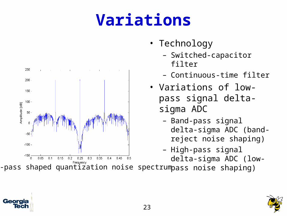
Variations• Technology
– Switched-capacitor filter– Continuous-time filter
• Variations of low-pass signal delta-sigma ADC– Band-pass signal delta-
sigma ADC (band-reject noise shaping)
– High-pass signal delta-sigma ADC (low-pass noise shaping)Band-pass shaped quantization noise spectrum
24
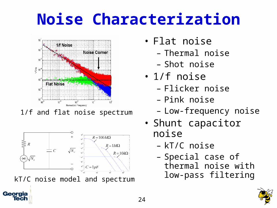
Noise Characterization• Flat noise
– Thermal noise– Shot noise
• 1/f noise– Flicker noise– Pink noise– Low-frequency noise
• Shunt capacitor noise– kT/C noise– Special case of
thermal noise with low-pass filtering
1/f and flat noise spectrum
kT/C noise model and spectrum
25
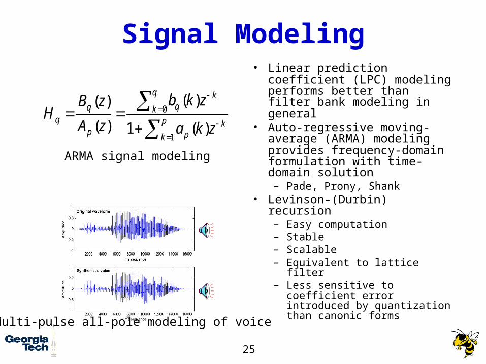
Signal Modeling
p
k
kp
q
k
kq
p
zka
zkb
zA
zBH
1
0
)(1
)(
)(
)(
• Linear prediction coefficient (LPC) modeling performs better than filter bank modeling in general
• Auto-regressive moving-average (ARMA) modeling provides frequency-domain formulation with time-domain solution– Pade, Prony, Shank
• Levinson-(Durbin) recursion– Easy computation– Stable– Scalable– Equivalent to lattice filter– Less sensitive to coefficient
error introduced by quantization than canonic forms
ARMA signal modeling
Multi-pulse all-pole modeling of voice
26
Research Proposal (1)• Investigate unified evaluation and
design criteria for ADCs– Comparison on Nyquist sampling
and oversampling ADCs with regard to flexibility, robustness, and system-on-chip integration
• Analog front-end evaluation– FE Modeling– Performance estimation– Architectural comparison
27
Research Proposal (2)• Analog-to-digital encoder and decoder
– Modeling ADC as encoder and search process
– Optimality of encoding and decoding• Delta-sigma modulator
– Decoding algorithm performance– Multidimensional space-time
architecture– Stability analysis– Mixed-signal processing schemes
28
Preliminary Research:Analog Front-end Evaluation
• Analysis on front-end (FE) of Analog-to-digital Converter (ADC)
• Function block models• FE Performance evaluation
29
Analysis on Analog FE of ADC
• Definitions of analog FE• Problem statement• Proposed FE function blocks
30
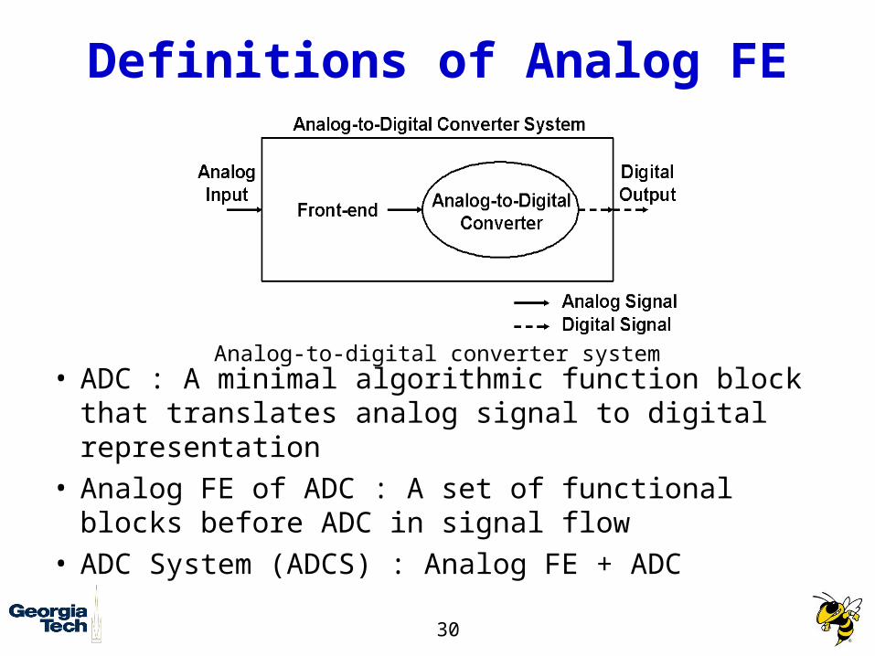
Definitions of Analog FE
• ADC : A minimal algorithmic function block that translates analog signal to digital representation
• Analog FE of ADC : A set of functional blocks before ADC in signal flow
• ADC System (ADCS) : Analog FE + ADC
Analog-to-digital converter system
31
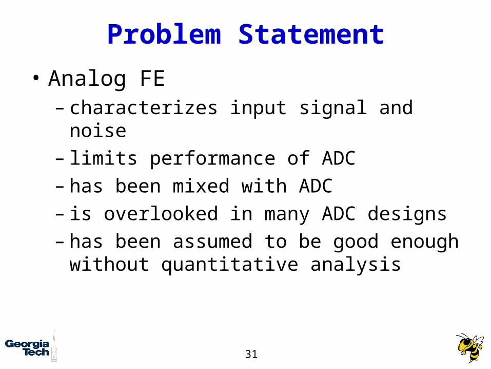
Problem Statement
• Analog FE – characterizes input signal and noise– limits performance of ADC– has been mixed with ADC– is overlooked in many ADC designs– has been assumed to be good enough
without quantitative analysis
32
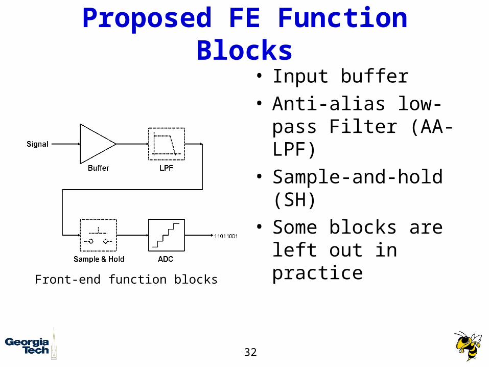
Proposed FE Function Blocks
• Input buffer• Anti-alias low-pass
Filter (AA-LPF)• Sample-and-hold
(SH)• Some blocks are
left out in practice
Front-end function blocks

33
Function Block Models
• Input buffer• Anti-alias low-pass filter• Sample-and-hold• Input signal• Signal and circuit noise• Continuous-time delta-sigma ADC
34
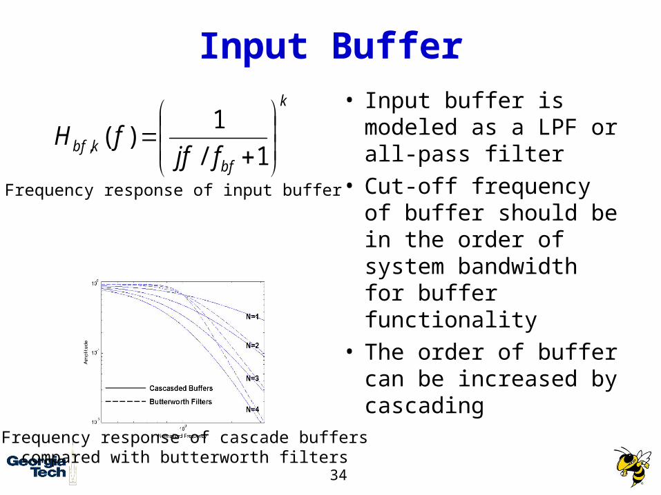
Input Bufferk
bfkbf fjffH
1/
1)(,
• Input buffer is modeled as a LPF or all-pass filter
• Cut-off frequency of buffer should be in the order of system bandwidth for buffer functionality
• The order of buffer can be increased by cascading
Frequency response of cascade bufferscompared with butterworth filters
Frequency response of input buffer

35
Anti-alias Low-pass Filter
1)/(
1|)(|
2,
,
k
klp
klpff
fH
• Implementation Types– Butterworth– Chebyshev– Elliptic
• Butterworth– Minimum pass-band
ripples– Less sensitive to filter
coefficient error
• Optimal cut-off frequency for maximum SNR against signal aliasing can be obtained
Butterworth filter frequency response
SNR available for filter cut-off frequency
36
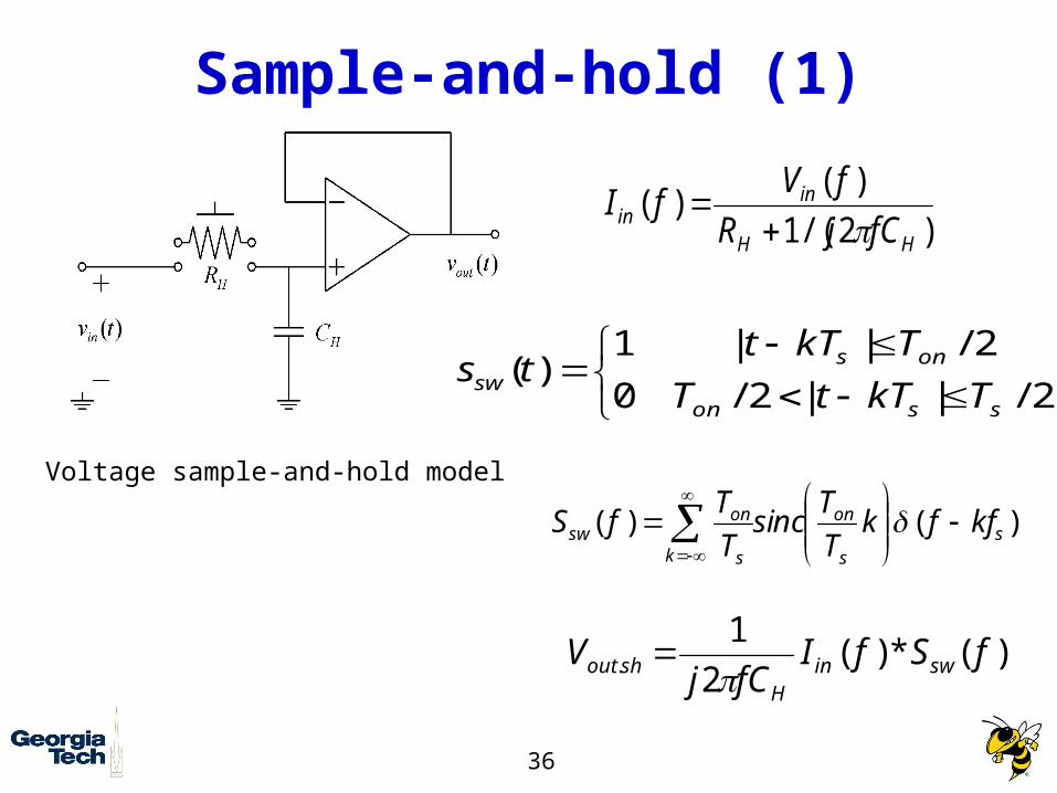
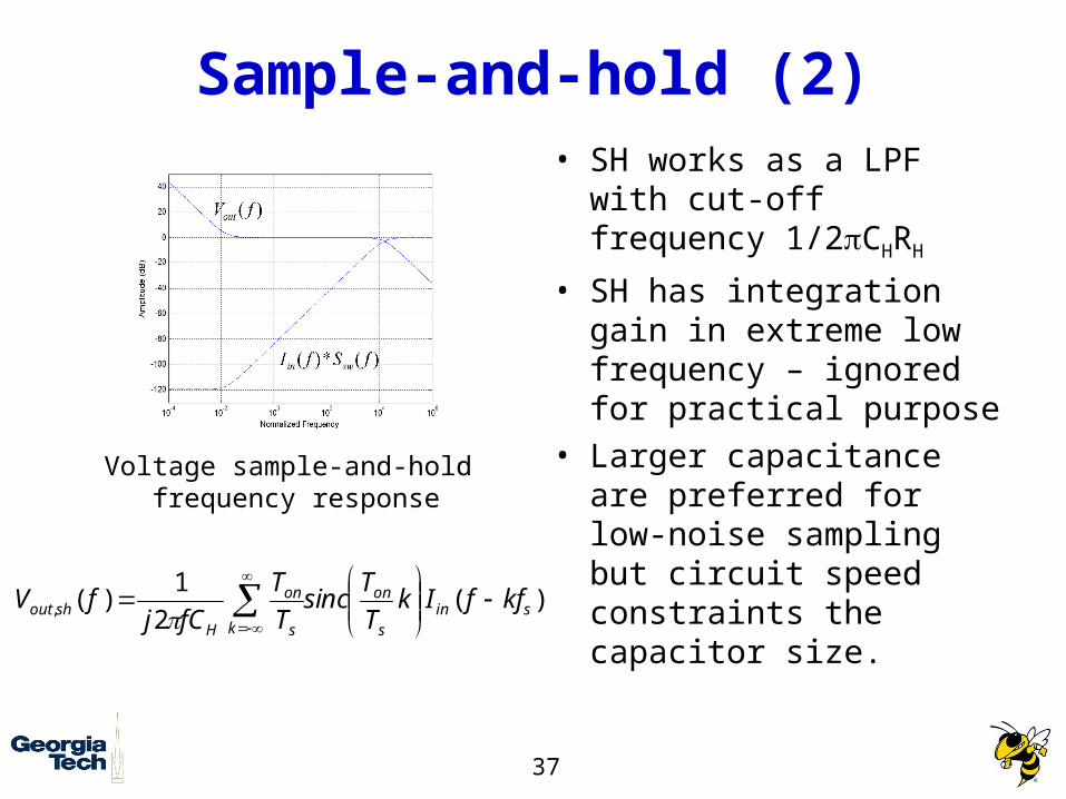
Sample-and-hold (1)
)2/(1
)()(
HH
inin fCjR
fVfI
2/||2/0
2/||1)(
sson
onssw TkTtT
TkTtts
)()( ss
on
k s
onsw kffk
T
Tncsi
T
TfS
)(*)(2
1. fSfI
fCjV swin
Hshout
Voltage sample-and-hold model
37
Sample-and-hold (2)• SH works as a LPF
with cut-off frequency 1/2CHRH
• SH has integration gain in extreme low frequency – ignored for practical purpose
• Larger capacitance are preferred for low-noise sampling but circuit speed constraints the capacitor size.
)(2
1)(, sin
s
on
k s
on
Hshout kffIk
T
Tncsi
T
T
fCjfV
Voltage sample-and-hold frequency response
38
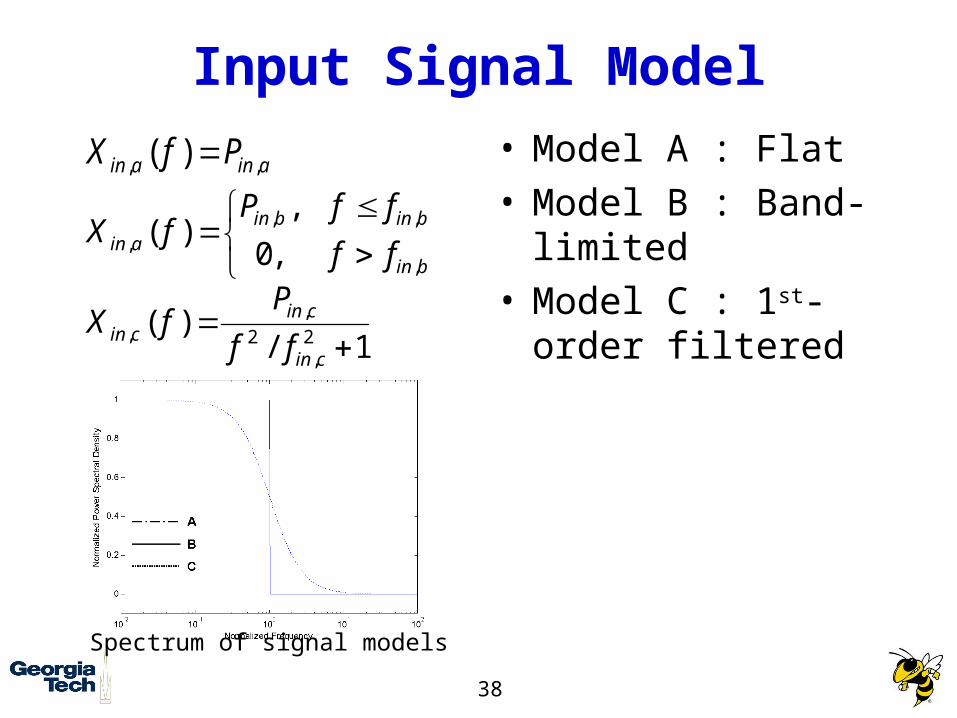
Input Signal Model• Model A : Flat• Model B : Band-
limited• Model C : 1st-order
filtered
ainain PfX ,, )(
bin
binbinain ff
ffPfX
,
,,, ,0
,)(
1/)(
2,
2
,,
cin
cincin ff
PfX
Spectrum of signal models
39
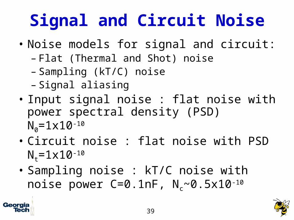
Signal and Circuit Noise• Noise models for signal and circuit:
– Flat (Thermal and Shot) noise– Sampling (kT/C) noise– Signal aliasing
• Input signal noise : flat noise with power spectral density (PSD) N0=1x10⁻¹⁰
• Circuit noise : flat noise with PSD Nt=1x10⁻¹⁰
• Sampling noise : kT/C noise with noise power C=0.1nF, Nc~0.5x10⁻¹⁰
40
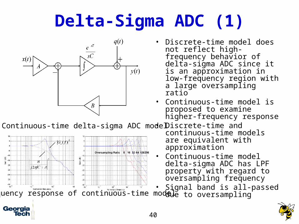
Delta-Sigma ADC (1)• Discrete-time model does
not reflect high-frequency behavior of delta-sigma ADC since it is an approximation in low-frequency region with a large oversampling ratio
• Continuous-time model is proposed to examine higher-frequency response
• Discrete-time and continuous-time models are equivalent with approximation
• Continuous-time model delta-sigma ADC has LPF property with regard to oversampling frequency
• Signal band is all-passed due to oversampling
Continuous-time delta-sigma ADC model
Frequency response of continuous-time model
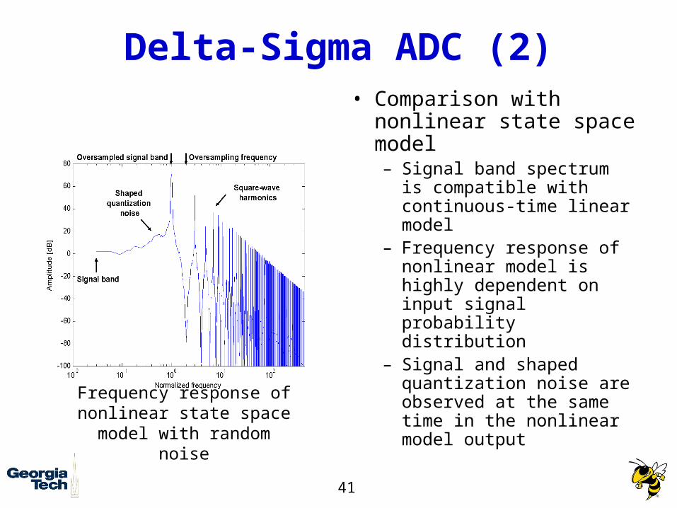
41
Delta-Sigma ADC (2)• Comparison with
nonlinear state space model– Signal band spectrum is
compatible with continuous-time linear model
– Frequency response of nonlinear model is highly dependent on input signal probability distribution
– Signal and shaped quantization noise are observed at the same time in the nonlinear model output
Frequency response of nonlinear state space
model with random noise
42
FE Performance Evaluation
• Oversampling assumption• Simulation method• Traditional FE• Direct SH FE without AA-LPF• Direct ADC FE without AA-LPF and SH• Summary
43
Oversampling Assumption• Input signal is regarded as stationary, quasi-
static, or dc when it is oversampled with high oversampling ratio
• Attenuation of input signal is enough at NfM (half of oversampling frequency) when a simple 1st-order LPF is used as an AA-LPF for oversampling, and residual signal aliasing is ignorable when it is folded over NfM (half of oversampling frequency)
• Digital domain multirate signal processing is powerful enough to avoid any signal aliasing during downsampling process
• Nominal oversampling ratio is 26 (64) ~ 210 (1024).
44
Simulation Method
• Frequency domain computation with cascading of function blocks
• Frequency step: 2x10⁻³
• Frequency range: 2x10²
• Signal and noise powers are obtained with numerical integration with extended and closed trapezoidal rule
• Performance measure: Signal-to-noise ratio (SNR)
45
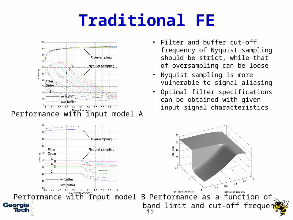
Traditional FE
Performance with input model A
Performance with input model B
• Filter and buffer cut-off frequency of Nyquist sampling should be strict, while that of oversampling can be loose
• Nyquist sampling is more vulnerable to signal aliasing
• Optimal filter specifications can be obtained with given input signal characteristics
Performance as a function of band limit and cut-off frequency
46
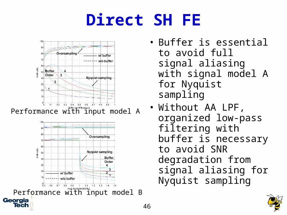
Direct SH FE• Buffer is essential
to avoid full signal aliasing with signal model A for Nyquist sampling
• Without AA LPF, organized low-pass filtering with buffer is necessary to avoid SNR degradation from signal aliasing for Nyquist sampling
Performance with input model A
Performance with input model B
47
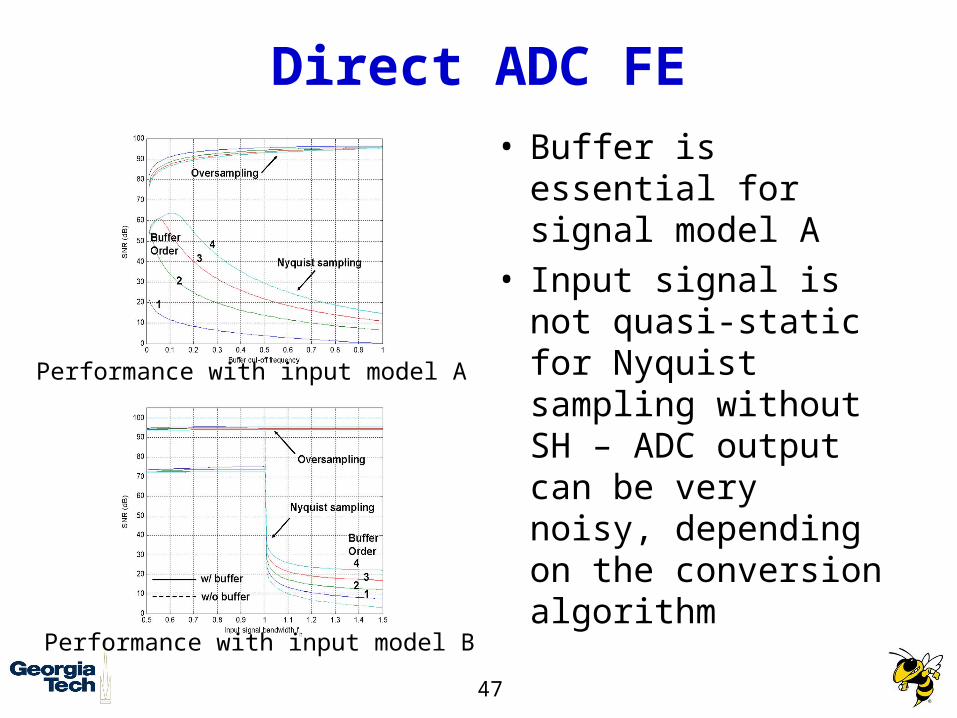
Direct ADC FE• Buffer is essential
for signal model A• Input signal is not
quasi-static for Nyquist sampling without SH – ADC output can be very noisy, depending on the conversion algorithm
Performance with input model A
Performance with input model B
48
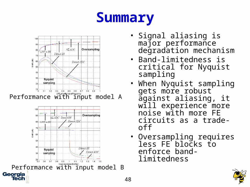
Summary• Signal aliasing is major
performance degradation mechanism
• Band-limitedness is critical for Nyquist sampling
• When Nyquist sampling gets more robust against aliasing, it will experience more noise with more FE circuits as a trade-off
• Oversampling requires less FE blocks to enforce band-limitedness
Performance with input model A
Performance with input model B
49
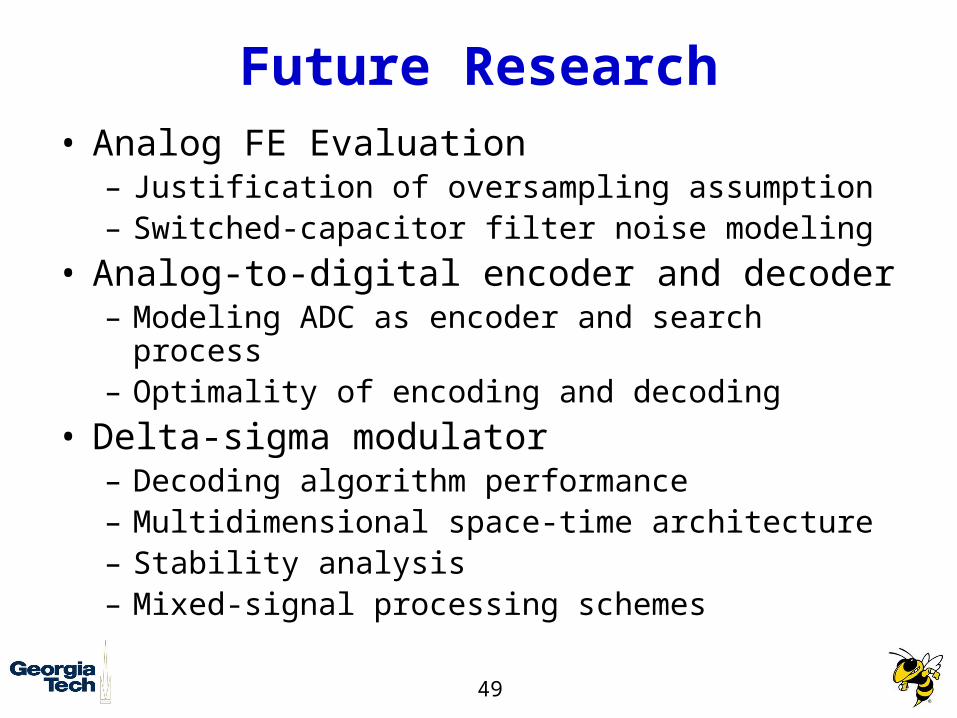
Future Research• Analog FE Evaluation
– Justification of oversampling assumption– Switched-capacitor filter noise modeling
• Analog-to-digital encoder and decoder– Modeling ADC as encoder and search process– Optimality of encoding and decoding
• Delta-sigma modulator– Decoding algorithm performance– Multidimensional space-time architecture– Stability analysis– Mixed-signal processing schemes
50
Research Publications• M. Thomas, J. Lillie, D. Kim, S. Ralph, N. Jokerst, M. Brooke, K. Dennis, B. Comeau, C.
Henderson, "An interferometric sensor for integration with Si CMOS signal processing circuitry: Sensor on a Chip", submitted to CLEO 2004
• Daeik D. Kim, Martin A. Brooke, "Modeling and Analysis of High-Pass Delta-Sigma Lock-In Analog-to-Digital Converter," submitted to ISCAS 2004
• Daeik D. Kim, Martin A. Brooke, "Comparison on the Performance of Decoding Schemes for Delta-Sigma Oversampling Converter," submitted to ISCAS 2004
• Daeik D. Kim, Martin A. Brooke, "Architectural Evaluation of Analog-to-Digital Converter Front-End Performance," submitted to ISCAS 2004
• Daeik D. Kim, Mikkel A. Thomas, Martin A. Brooke, Nan M. Jokerst, "Integration of Si-CMOS Embedded Photo Detector Array and Mixed Signal Processing System with Embedded Optical Waveguide Input", under preparation for SPIE Integrated Optoelectronic Devices 2004 Symposium
• Daeik D. Kim, Martin A. Brooke, "A 1.4G Samples/sec Comb Filter Design for Decimation of Sigma-Delta Modulator Output," Proc. 2003 IEEE ISCAS, pp.1009-1012
• N. Jokerst, M.A. Brooke, A.S. Brown, S.Y. Cho, R. Huang, S.W. Seo, M. Thomas, I. Song, S.H. Hyun, D.I. Kim, "Optoelectronic Microsystems integration for systems on a package and systems on chip applications," 2002 OSA Annual Meeting, TuV1, Orlando, Florida, Oct 2002 (Invited)
• J. Lillie, D. Kim, M. Thomas, M.A. Brooke, N.M. Jokerst, S.E. Ralph, "Highly multimode interferometric sensors," 2002 OSA Annual Meeting, TuL37, Orlando, Florida, Oct 2002
• Sang-Yeon Cho, Mikkel Thomas, Dae-Ik Kim, Nan M. Jokerst, Martin A. Brooke, “Polymer Waveguide Optical Interconnections on Si CMOS Circuits,” CtuF2, Conference on Lasers and Electro-Optics, Long Beach, CA, p.161, 2002
51
Conclusion
• Overview• Literature review• Research proposal• Analog FE modeling and performance
evaluation as a preliminary research• Future research

Questions ?Comments ?
Design of Robust and Flexible On-chip Analog-to-Digital Conversion
Architecture
Supplemental Slides forPh. D. Dissertation Proposal Presentation
of Daeik Kim
Advisor : Prof. Martin BrookeBOSS Team : Dr. N. Jokerst, Dr. S. Ralph
Dr. C. Henderson
School of Electrical and Computer EngineeringGeorgia Institute of Technology
54
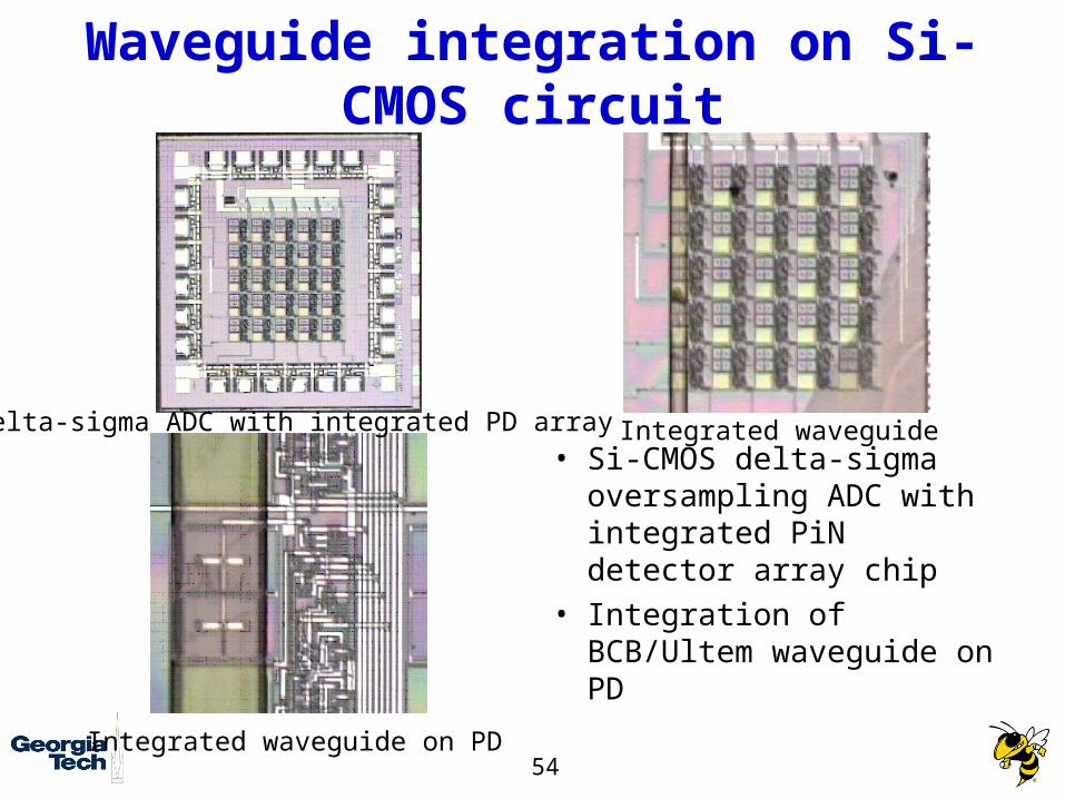
Waveguide integration on Si-CMOS circuit
• Si-CMOS delta-sigma oversampling ADC with integrated PiN detector array chip
• Integration of BCB/Ultem waveguide on PD
Delta-sigma ADC with integrated PD array Integrated waveguide
Integrated waveguide on PD
55
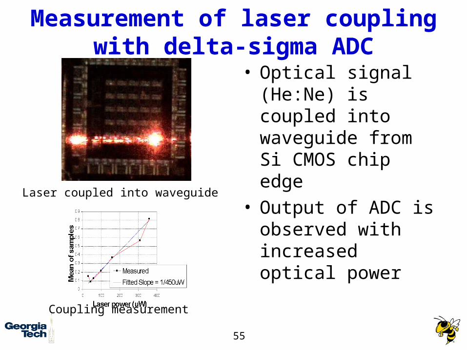
Measurement of laser coupling with delta-sigma ADC
• Optical signal (He:Ne) is coupled into waveguide from Si CMOS chip edge
• Output of ADC is observed with increased optical power
Laser coupled into waveguide
Coupling measurement
56
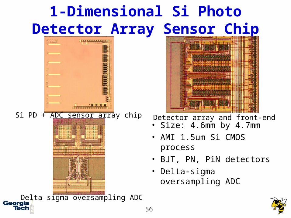
1-Dimensional Si Photo Detector Array Sensor Chip
• Size: 4.6mm by 4.7mm• AMI 1.5um Si CMOS
process• BJT, PN, PiN detectors• Delta-sigma
oversampling ADC
Detector array and front-endSi PD + ADC sensor array chip
Delta-sigma oversampling ADC
57
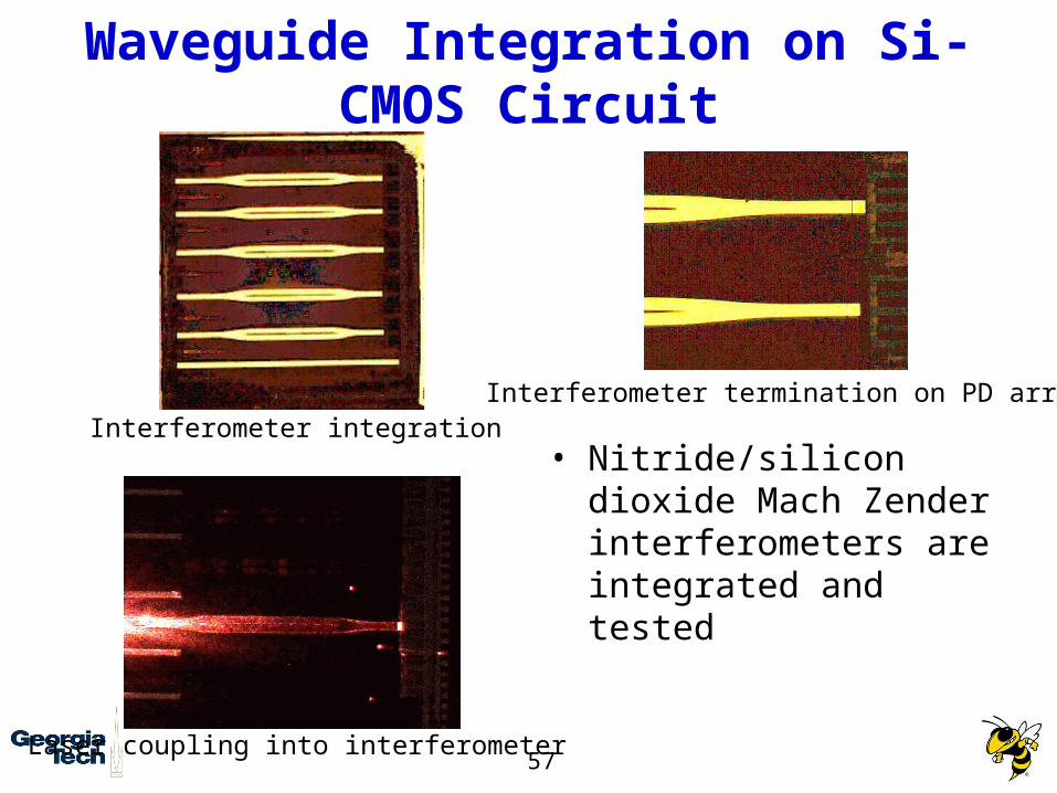
Waveguide Integration on Si-CMOS Circuit
• Nitride/silicon dioxide Mach Zender interferometers are integrated and tested
Interferometer integrationInterferometer termination on PD array
Laser coupling into interferometer
58
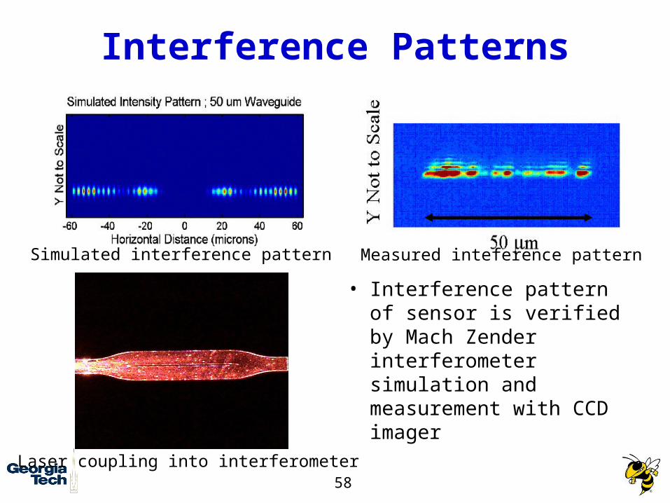
Interference Patterns
• Interference pattern of sensor is verified by Mach Zender interferometer simulation and measurement with CCD imager
Simulated interference pattern Measured inteference pattern
Laser coupling into interferometer
59
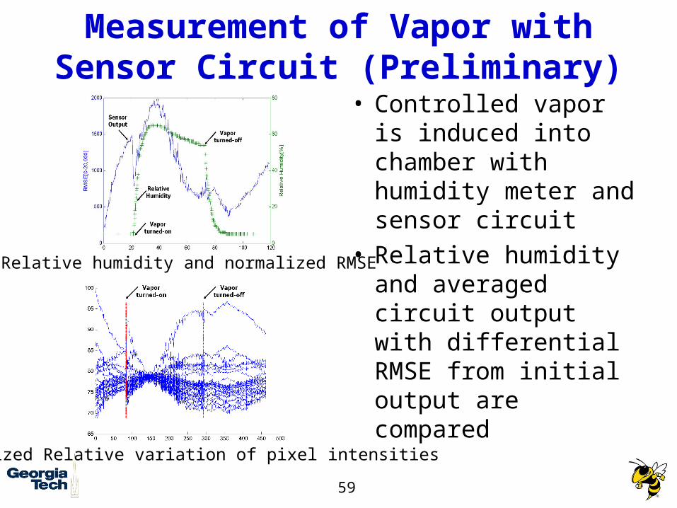
Measurement of Vapor with Sensor Circuit (Preliminary)
• Controlled vapor is induced into chamber with humidity meter and sensor circuit
• Relative humidity and averaged circuit output with differential RMSE from initial output are compared
Relative humidity and normalized RMSE
Normalized Relative variation of pixel intensities
60
Work to be done
• Minimize side-effects from mechanical movement, light source drift, and chemical reaction of sensor set up
• De-correlate side-effects from measurement data
• Run sensor test with several active agents
• Integrate laser on the chip for a complete system and run sensor tests
61
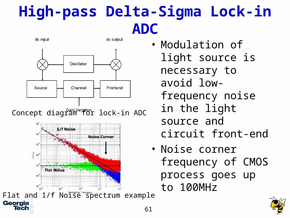
High-pass Delta-Sigma Lock-in ADC
• Modulation of light source is necessary to avoid low-frequency noise in the light source and circuit front-end
• Noise corner frequency of CMOS process goes up to 100MHz
Concept diagram for lock-in ADC
Flat and 1/f Noise spectrum example

62
High-pass Delta-Sigma ADC• High-pass delta-
sigma ADC shapes quantization noise to low-pass region while preserve high-pass signal1st-order high-pass delta-sigma ADC
High-pass delta-sigma shaped noise spectrum
63
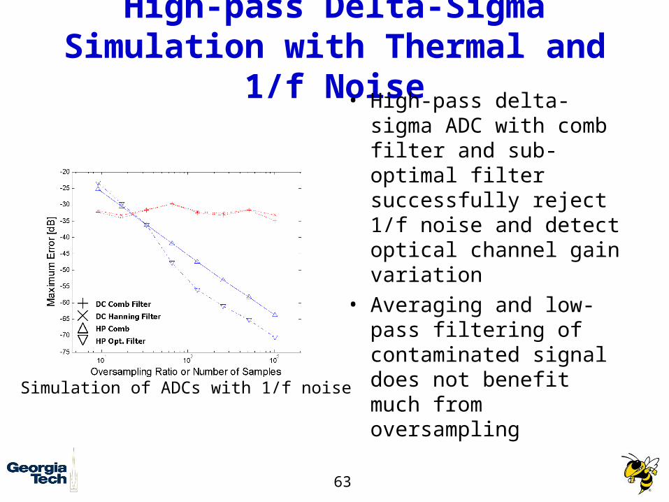
High-pass Delta-Sigma Simulation with Thermal and
1/f Noise• High-pass delta-sigma ADC with comb filter and sub-optimal filter successfully reject 1/f noise and detect optical channel gain variation
• Averaging and low-pass filtering of contaminated signal does not benefit much from oversampling
Simulation of ADCs with 1/f noise
64
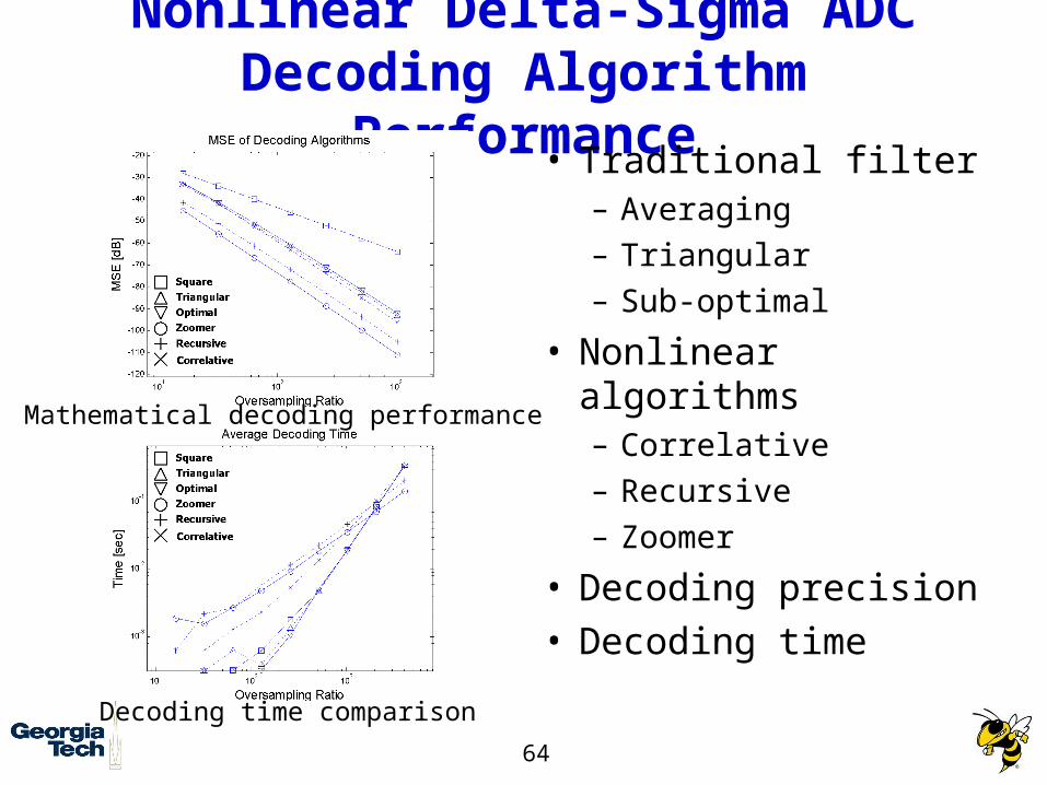
Nonlinear Delta-Sigma ADC Decoding Algorithm
Performance• Traditional filter– Averaging– Triangular– Sub-optimal
• Nonlinear algorithms– Correlative– Recursive– Zoomer
• Decoding precision• Decoding time
Mathematical decoding performance
Decoding time comparison
65
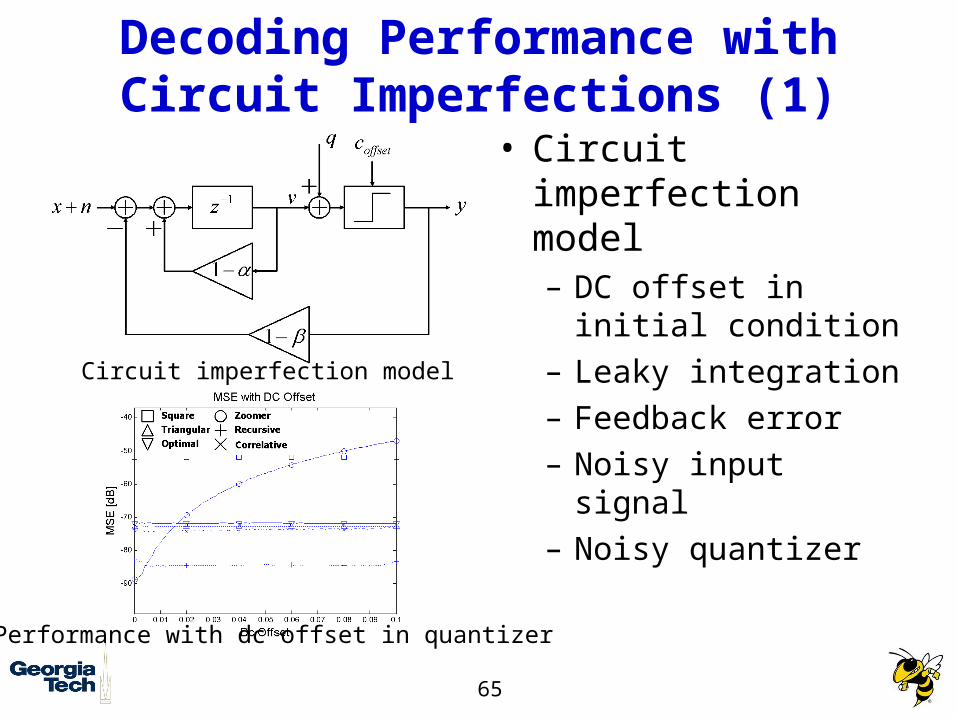
Decoding Performance with Circuit Imperfections (1)
• Circuit imperfection model– DC offset in initial
condition– Leaky integration– Feedback error– Noisy input signal– Noisy quantizer
Circuit imperfection model
Performance with dc offset in quantizer

66
Decoding Performance with Circuit Imperfections (1)
• Circuit imperfection model– DC offset in initial
condition– Leaky integration– Feedback error– Noisy input signal– Noisy quantizer
Circuit imperfection model
Performance with dc offset in quantizer
67
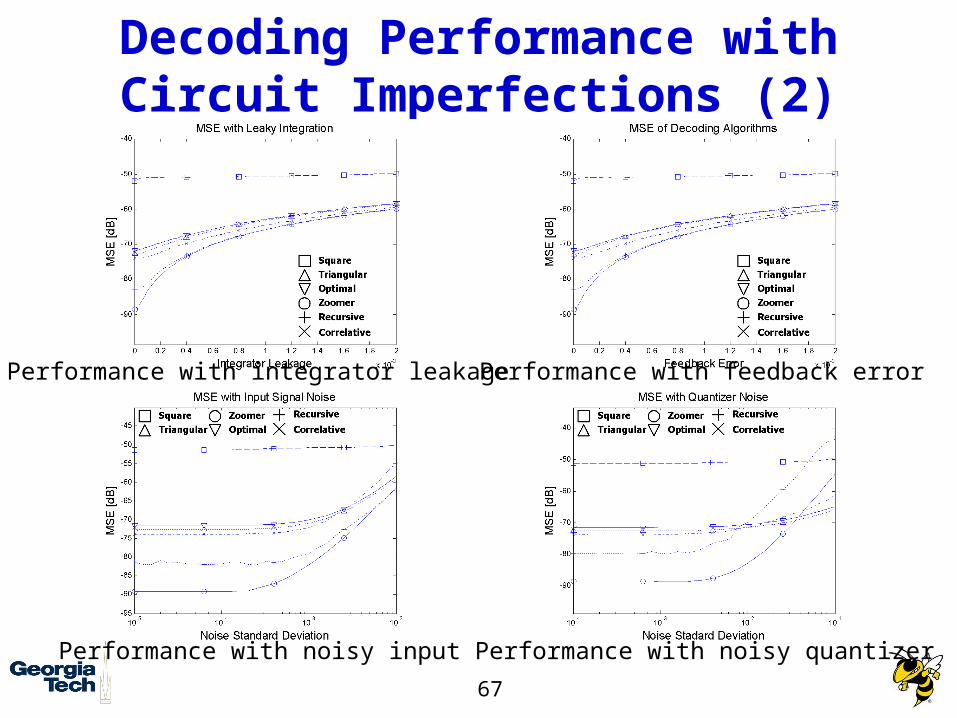
Decoding Performance with Circuit Imperfections (2)
Performance with integrator leakage Performance with feedback error
Performance with noisy input Performance with noisy quantizer