routing for analog chip design at nxp semiconductors
TRANSCRIPT

Routing for analog chip design at NXPsemiconductors
Marjan van den Akker
Theo Beelen
Rob H. Bisseling
Bas Fagginger Auer
Frederik von Heymann
Tobias Muller
Joost Rommes
Technical Report UU-CS-2011-011
May 2011
Department of Information and Computing Sciences
Utrecht University, Utrecht, The Netherlands
www.cs.uu.nl

ISSN: 0924-3275
Department of Information and Computing Sciences
Utrecht University
P.O. Box 80.089
3508 TB UtrechtThe Netherlands
Routing for analog chip designs at NXP
Semiconductors
Marjan van den Akker∗ Theo Beelen† Rob H. Bisseling‡
Bas Fagginger Auer‡ Frederik von Heymann§
Tobias Muller¶ Joost Rommes†
May 10, 2011
Abstract
During the study week 2011 we worked on the question of how toautomate certain aspects of the design of analog chips. Here we focusedon the task of connecting different blocks with electrical wiring, which isparticularly tedious to do by hand. For digital chips there is a wealth ofresearch available for this, as in this situation the amount blocks makesit hopeless to do the design by hand. Hence, we set our task to findingsolutions that are based on the previous research, as well as being tailoredto the specific setting given by NXP.
This resulted in a heuristical approach, which we presented at theend of the week in the form of a protoype tool. In this report we give adetailed account of the ideas we used, and describe possibilities to extendthe approach.
1 Introduction
1.1 NXP Semiconductors
NXP Semiconductors N.V. (Nasdaq: NXPI) is a global semiconductor companyand a long-standing supplier in the industry, with over 50 years of innovationand operating history. The company provides high-performance electronic chips
∗Department of Information and Computing Sciences, Utrecht University, P.O. Box 80089,3508TB Utrecht, the Netherlands†NXP Semiconductors Netherlands N.V., High Tech Campus 46, 5656AE Eindhoven, the
Netherlands‡Department of Mathematics, Utrecht University, P.O. Box 80010, 3508TA Utrecht, the
Netherlands§Department of Applied Mathematics, Delft University of Technology, P.O. Box 5031,
2600GA Delft, the Netherlands¶Centrum Wiskunde & Informatica, P.O. Box 94079, 1090GB Amsterdam, the Netherlands
1

to its customers, and produces these building on its expertise in the areas of RF,analog and digital circuits, power management, and security. These innovationsare used in a wide range of automotive, identification, wireless infrastructure,lighting, industrial, mobile, consumer and computing applications. Headquar-tered in Europe, the company has approximately 28,000 employees working inmore than 25 countries and posted sales of USD 3.8 billion in 2009.
1.2 Place and route for analog designs
The increasing demand for smaller, faster, and multi-functional electronic de-vices such as smart phones is one of the driving forces in the semiconductorindustry. Combined with requirements on power usage, sustainability, and wire-less functionality this is generating challenges in several domains. During thedesign of the layout, which is a representation of the chip in shapes in its physicallayers (silicon, oxide, metal), one of the challenges is to place and route (wire)the circuit components in an optimal way. Aspects that define optimality mayvary per design/application and are typically related to the area (convex hull)of the chip, the total wire length, and the unintended side-effects caused bythe wires (crosstalk, i.e., electrical fields between wires). The place and routeproblem is further complicated by design rules and geometrical constraints.
The place and route problem has been studied for many years and maturesolutions are available for digital designs [1, 4, 10, 11, 12, 15, 16, 17, 21], whichtypically consist of (almost) equally sized blocks and predefined routing chan-nels. For analog designs, the main interest of NXP, the place and route problemis more complicated because blocks can vary in size and aspect ratio and mayeven overlap (so that there is no need for explicit routing), and because routingchannels are typically not available but defined by the placement. Also, whiletypically several layers (metal) are available to route in, often one would liketo limit this to as few layers as possible, and in some cases routing is even re-stricted to a single layer. Other objectives one can think of are to minimize thewire length and the number of turns in the wires, and typical constraints arethat wires are either horizontal or vertical (only 90-degree turns) and shouldbe of a certain minimum distance from each other. Furthermore, it is desirableto have a routing algorithm that is robust with respect to (small) changes inthe layout, so that it can be used in parametrized designs to update the routingautomatically when parameters change – this allows designers to quickly exploredifferent physical design variants.
The challenge NXP set for the study week of 2011 was to develop an algo-rithm that, given a number of circuit blocks and their interconnections, com-putes an optimal layout including placement and routing.
1.3 Outline
In Section 2 we describe the precise task we discussed during the study week, andwe give a detailed account of the partial results we were able to achieve, includingthe prototype of a tool that we think can simplify the work of chip designers. In
2

Section 3 we give an overview of possible extensions and improvements of oneparticular aspect of our algorithm, which we believe could be a computationalbottleneck for larger instances; Section 4 outlines a slightly more sophisticatedalgorithm than the one in Section 2, which also has the benefit of giving us lowerbounds on the quality of the solutions it produces. We conclude the report witha summary of our results and an estimation of the success in terms of the originalchallenge.
2 Heuristic Method and Implementation
As illustration of the ideas developed for NXP during the study week, we im-plemented a heuristic for solving the problem as a C++ program. An earlyversion of this program was demonstrated during the final presentation sessionof the study week as well as a later version during a visit to NXP in Eindhoven(Figure 1).
Because of the time constraints of the study week we chose to focus only onthe routing aspect of NXP’s problem: the program should be able to importa layout specified in NXP’s circuit design software (Figure 2), where all thecomponents have already been placed on the chip, and export routing in theform of wires connecting these components (thin wires in Figure 1). Wires areformed on the circuit by depositing metal in the production process.
The circuits are produced layer-by-layer, so we know beforehand that thereis an l ∈ N specifying the number of layers (l = 5 in Figure 1) and a boundingbox of the entire circuit board within which all components and wiring should becontained. We do not want to short-circuit different components on the circuitboard by placing metal at the wrong places, therefore we receive for each layer anumber of solid rectangles, in which no metal can be deposited (solid gray blocksin Figure 1). These rectangles are characterized by their lower-left and upper-right corners in R2, as well as the number of the layer in which they are present.The components in the circuit need to be connected by conducting metal: weare given a list of pins, conducting rectangles belonging to a certain layer andhaving a certain color (the colored blocks in Figure 1). All pins sharing thesame color should be connected by metal. To prevent accidental short-circuitingand interference, wires should have a minimum distance from each other; theseminima can be different for different layers, so they are represented by a vectorδ ∈ Rl
>0. It is important to note that wires are not restricted to a single layer:wires can make jumps to other layers by vias.
Our program now needs to find out, given these parameters, where to depositmetal in the circuit such that
• for each pair of pins sharing the same color there exists a continuous metalpath connecting the pins;
• the distance between two bits of deposited metal in the same layer k thatare connecting pins with different colors is always ≥ δk;
3
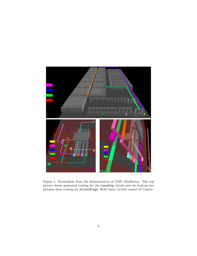
Figure 1: Screenshots from the demonstration at NXP, Eindhoven. The toppicture shows generated routing for the tunedCap circuit and the bottom twopictures show routing for difInvStage. Both these circuits consist of 5 layers.
4
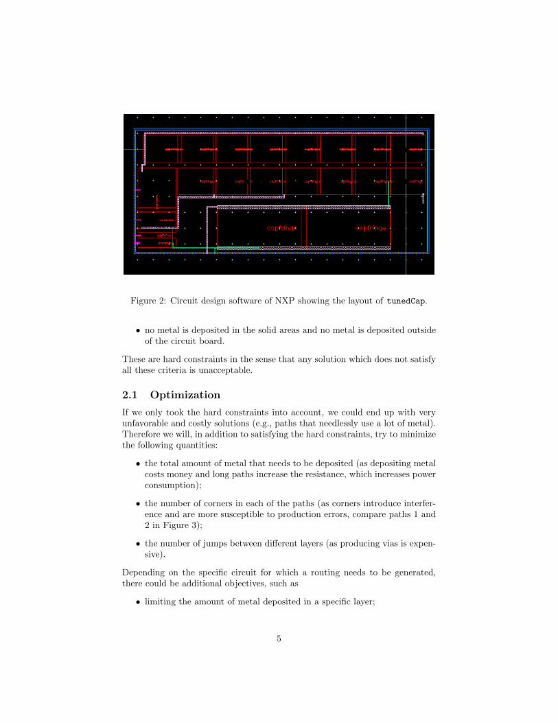
Figure 2: Circuit design software of NXP showing the layout of tunedCap.
• no metal is deposited in the solid areas and no metal is deposited outsideof the circuit board.
These are hard constraints in the sense that any solution which does not satisfyall these criteria is unacceptable.
2.1 Optimization
If we only took the hard constraints into account, we could end up with veryunfavorable and costly solutions (e.g., paths that needlessly use a lot of metal).Therefore we will, in addition to satisfying the hard constraints, try to minimizethe following quantities:
• the total amount of metal that needs to be deposited (as depositing metalcosts money and long paths increase the resistance, which increases powerconsumption);
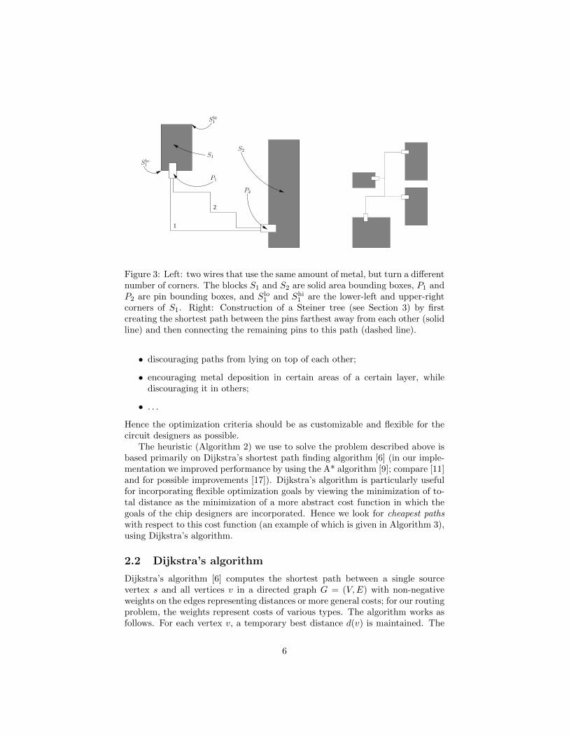
• the number of corners in each of the paths (as corners introduce interfer-ence and are more susceptible to production errors, compare paths 1 and2 in Figure 3);
• the number of jumps between different layers (as producing vias is expen-sive).
Depending on the specific circuit for which a routing needs to be generated,there could be additional objectives, such as
• limiting the amount of metal deposited in a specific layer;
5
2
1
P2
P1
S2
S1
Shi
1
S lo
1
Figure 3: Left: two wires that use the same amount of metal, but turn a differentnumber of corners. The blocks S1 and S2 are solid area bounding boxes, P1 andP2 are pin bounding boxes, and Slo
1 and Shi1 are the lower-left and upper-right
corners of S1. Right: Construction of a Steiner tree (see Section 3) by firstcreating the shortest path between the pins farthest away from each other (solidline) and then connecting the remaining pins to this path (dashed line).
• discouraging paths from lying on top of each other;
• encouraging metal deposition in certain areas of a certain layer, whilediscouraging it in others;
• . . .
Hence the optimization criteria should be as customizable and flexible for thecircuit designers as possible.
The heuristic (Algorithm 2) we use to solve the problem described above isbased primarily on Dijkstra’s shortest path finding algorithm [6] (in our imple-mentation we improved performance by using the A* algorithm [9]; compare [11]and for possible improvements [17]). Dijkstra’s algorithm is particularly usefulfor incorporating flexible optimization goals by viewing the minimization of to-tal distance as the minimization of a more abstract cost function in which thegoals of the chip designers are incorporated. Hence we look for cheapest pathswith respect to this cost function (an example of which is given in Algorithm 3),using Dijkstra’s algorithm.
2.2 Dijkstra’s algorithm
Dijkstra’s algorithm [6] computes the shortest path between a single sourcevertex s and all vertices v in a directed graph G = (V,E) with non-negativeweights on the edges representing distances or more general costs; for our routingproblem, the weights represent costs of various types. The algorithm works asfollows. For each vertex v, a temporary best distance d(v) is maintained. The
6

distance d(v) is lowered each time a shorter path to v is encountered. Thepredecessor of v in that path is then registered, thus storing the shortest path,and not only its cost. At some stage in the computation, the distance reachesits final value, the shortest distance to v. Then, v is included in the set D offinished vertices. Initially, d(s) = 0, d(v) = ∞ for v 6= s, and D = ∅. It canbe shown that the distance obtains its final value once d(v) = minw∈V−D d(w).Algorithm 1 presents Dijkstra’s algorithm.
Algorithm 1 Dijkstra’s Algorithm.
Input: Directed graph (V,E) with costs c(v, w) ≥ 0 for every edge (v, w) ∈ E,source vertex s ∈ V .
Output: The cost d(v) for reaching vertex v from s, and a predecessor in ashortest path to v, for every v ∈ V .
1: for all v ∈ V do2: d(v)←∞;3: pred(v)← v;4: d(s)← 0;5: D ← ∅;6: while D 6= V do7: v ← argmin{d(w) : w ∈ V −D};8: D ← D ∪ {v};9: for all w with (v, w) ∈ E do
10: if d(v) + c(v, w) < d(w) then11: d(w)← d(v) + c(v, w);12: pred(w)← v;
The A* algorithm is a more efficient variant of Dijkstra’s algorithm, whichmakes use of knowledge about a target vertex t that we want to reach, suchas a lower bound l(v) on the cost of reaching t. In our case, we will use theminimum distance to be covered on a three dimensional grid (see the nextsection) as a lower bound, ignoring other costs. The bound is called consistentif l(v) ≤ c(v, w) + l(w) for all (v, w) ∈ E. For our problem, the bound isconsistent because c(v, w) includes the distance cost of routing from v to w.Algorithm 1 can be changed from Dijkstra to A* by writing t /∈ D instead ofD 6= V on line 6 and d(w) + l(w) instead of d(w) on line 7.
2.3 Implementation
Algorithm 2 outlines the heuristic employed by the prototype tool. In the al-gorithm we deposit metal of certain colors in order to be able to differentiatebetween wires connecting different sets of pins. Two deposited wires that do notshare the same color should always be separated by the minimum separationdistance as specified by δ. For bounding boxes we use the following notation:if B is a bounding box, then Blo, Bhi ∈ R2 are the lower-left and upper-rightcorner of the bounding box, respectively. The layer where the bounding box is
7

present is indicated by Blayer ∈ N.
Algorithm 2 Discretization and Heuristic Wiring.
Input: Number of layers l ∈ N, minimum wire separation δ ∈ Rl>0, circuit
board bounding box B, solid area bounding boxes S1, S2, . . . , pin boundingboxes P1, P2, . . . .
Output: Discretized grid in which the metal depositions have been marked.1: Let ρ← grid spacing based on δ or a specified resolution;2: Create three-dimensional grid G of d(Bhi −Blo)/ρe by l cells;3: for all solid area bounding boxes S do4: Mark all cells lying between b(Slo −Blo)/ρc and d(Shi −Blo)/ρe in layer
Slayer as inaccessible for all colors;5: for all pins P do6: Mark all cells lying between b(P lo−Blo)/ρc and d(P hi−Blo)/ρe in layer
P layer as metal with color P color;7: Mark all cells within distance dδP layer/ρe of P as inaccessible, except for
color P color;8: Sort pins by their color into nets and then the nets by increasing bounding
box volume;9: for all nets P in which all pins share the same color Pcolor do
10: Find P1, P2 ∈ P such that the distance between the centers of P1 and P2
is maximal;11: Create a cheapest path T ⊆ G from P1 to P2 traversing only cells acces-
sible for color Pcolor;12: Similarly create cheapest paths from T to all P ∈ P not connected to T
and add these paths to T ;13: for all cells c ∈ T do14: Mark c as metal with color Pcolor;15: Mark all cells in layer cz with distance ≤ dδcz/ρe to c as inaccessible,
except for color Pcolor;16: Output G;
To simplify the problem we first discretize it (line 2) to a regular three-dimensional grid G, with l layers and spacing ρ within each layer. G will be thegraph in which we perform Dijkstra’s path-finding algorithm. Cells c ∈ G havethree coordinates (cx, cy, cz) ∈ Z3, where 1 ≤ cz ≤ l is the layer in which the cellresides. To ensure that we never deposit metal in solid regions, we mark thesein G first by discretizing the bounding boxes and flagging the cells containedin them as inaccessible for metal from any pin. We then proceed at line 5 toadd all pins, marking the cells contained in them as metal of the pin’s color andensuring that no metal belonging to pins with a different color can be depositednear the pin (as this could violate the minimum separation criterion).
After the solid regions and pins have been marked, we generate paths con-necting all the pins sharing the same color at line 8. First we cluster the pinstogether such that we have nets of pins all sharing the same color. Note that the
8

algorithm will yield different results if we connect the pins contained in thesenets in a different order, hence we will fix the ordering by sorting the nets ofpins of the same color by the volume of the bounding box containing the pins.This idea originates from the fact that connecting all the short paths first willlead to less conflicts between paths later than first connecting all the long paths(which could potentially cut off short paths).
Then we will connect, for each net of pins sharing the same color, the pinsbelonging to this net. If there are at most two pins in a net, we can directlyuse Dijkstra’s algorithm to find the cheapest path connecting them. However, ifwe have more than two pins, we need to generate a Steiner tree (see Section 3)connecting all of them. In our heuristic, this is done by first creating a pathbetween the two pins that are farthest apart, and then using this long pathas a ‘trunk’ to which the remaining, unconnected, pins connect as branches viaDijkstra’s algorithm (see the right panel of Figure 3). A path can only be createdalong cells that are accessible for the particular color of the current path; thisto ensure that the minimum separation distance is always maintained.
Algorithm 3 Routing Cost Function for Dijkstra’s Algorithm.
Input: Neighboring cells c−1, c0, and c1 in the grid G where c−1 is the prede-cessor of c0.
Output: The cost k to use cell c1 to continue the path.1: Initialize k ← 0;2: if c1 is not marked as metal then3: We need to deposit metal: k ← k + kmetal;4: if cz1 6= cz0 then5: We need to create a via: k ← k + kvia;6: if ‖c1 − c−1‖2 = 2 then7: We turn a corner if we continue this way: k ← k + kcorner;8: . . .9: Output k;
Algorithm 3 gives a simple example cost function for Dijkstra’s algorithmwhere we consider continuing an existing path going through cells . . .→ c−1 →c0 to c0’s neighbor c1 (neighbor in the sense that ‖c1 − c0‖ = 1). The costcan be influenced by varying three parameters: kmetal, kcorner, and kvia. Thisallows the designer to indicate whether he finds minimizing the length of thewires (increasing kmetal), minimizing the number of corners (increasing kcorner),or minimizing the number of vias (increasing kvia) more important. In Figure 1the colored bars on the left are similar cost modifiers, from bottom to top: costto deposit metal, cost to turn a corner, cost to create a via, cost to run overan existing wire, and cost to run over a solid block. By extending the costfunction and permitting the designers to vary the associated weights, a numberof different routing suggestions is easily obtained from the program. Note thatthe multiplicative factors such as kmetal can also be made to depend on theposition of c0 or c1, permitting the designer to make certain layers or certain
9

regions of layers more or less attractive for the wires to traverse; this and othercosts can be added at line 8.
The program prototype has been demonstrated to circuit designers of NXPin Austria and its source code has been provided to NXP.
3 Some Ideas for Steiner Trees
As we mentioned above, if we have more than two pins in one net, we cannotjust use Dijkstra’s algorithm to connect them. If we consider the pure problemof only one set of pins to be connected, this is an instance of the Steiner treeproblem. Given a set of vertices, called terminals (which will be our pins), andanother set of vertices, called Steiner points (grid points that are not blocked),a Steiner tree is any tree that contains all terminals and (some) Steiner points.
This section will give a brief account of possibilities to find a good Steinertree in a grid (with obstacles). In particular this means that here we ignorethe fact that it might not be possible (depending on the layout) to achieve anoptimal routing solution by considering the nets successively. We defer thisdiscussion to the next section.
As is true for most aspects of chip design, it is a computationally hard prob-lem to find a smallest Steiner tree [7], and there is an abundance of strategiesto get reasonably good approximations in acceptable time [2, 18]; and for morealgorithms, see [10, 11, 12, 15]. Here we will restrict our attention to approachesthat seem appealing because of their simple implementability and their compat-ibility with the strategy we chose for paths.
Most algorithms we found in the literature deal with the rectilinear versionof the Steiner tree problem, i.e., where all terminals and Steiner points aregiven in a two-dimensional rectilinear grid. As we want to find Steiner treesin a three-dimensional grid (with obstacles), these results are to be taken withsome caution, although we believe that on average they are close to what is tobe expected for our setup. The idea presented in the previous section can beseen as a simplification of ideas from [10], where it is stated that we will get atree that is at most a factor of 3/2 away from a minimal Steiner tree, and onaverage much closer to it.
It should, however, be mentioned that the authors in [10] consider nets thatinclude a source. In such a case it is usually desirable to minimize the distanceof the other pins to the source, whereas our focus is more on the total (weighted)wire-length used in the tree. In the former case one typically gets star-shapedtrees, whereas in the latter a caterpillar-structure is more likely.
As long as the net contains at most 6 pins, a rectilinear Steiner minimaltree in an obstacle-free grid can be found by going through all permutationsof the order of pins, connecting them in these orders in the way described inSection 2.3. For larger nets, this approach will not always produce an optimaltree (not even in this special case of obstacle-free rectilinear trees), but there aregood approximations available [14]. Still restricted to the rectilinear case, andgiven that the instances are typically relatively small in the case of analog chip
10

design, one can also consider computing a truly minimal Steiner tree, using,e.g., GeoSteiner [19, 20]. For more information, the paper by Hentschke et al.[11] is a good survey on exact results and approximations for rectilinear Steinertrees, taking into account different priorities of optimization.
4 Integer Programming and Approximations
In this section we propose a mathematically more rigorous approach, whichextends our heuristic from Section 2 but was too elaborate to incorporate in theprototype tool during the short time span of the study week.
This is a column generation approach (which can also be found in [10] insomewhat similar form), an approach that has successfully been applied to dif-ferent real-world optimization problems (see [5]). While we give all formulationsin terms of paths between pairs of pins, they work (with one limitation) also forlarger nets.
4.1 Column Generation
Let us start with decomposing the problem into two levels. The top (or master)level is the following: given all nets and for each a pool of paths connectingthem (possibly all such paths), we want to select one path for each net, suchthat the resulting wiring satisfies our hard constraints and is of high qualitywith respect to the optimization goals.
This is an integer linear program (see precise formulation below), which isknown to be computationally hard to solve to optimality [13]. And while theanalog design is not excessively large, here we get a huge number of variables:one for each pair of a net and a possible path for this net.
We note here that one can reduce the size of the graph involved by using lessvertices and introducing different weights on the edges depending of the capacityof the space between the vertices. One could construct such a graph with aGeneralized Voronoi Diagram. This method has been used for path planningin games (see, e.g., [8]), where characters have to move through a landscapeand avoid obstacles. In chip design, electrons move through the wires and avoidcomponents (except for the locations of their pins). We can define a GeneralizedVoronoi Diagram around the components. The edges in this diagram result in acollection of corridors going through the central areas of the open space betweenthe components. In this way, they result in edges for our routing network. Foreach pin we add an edge representing the shortest line connecting that pinto the network. In general, this network will be smaller in terms of verticesand edges than the grid which is attractive from a computational point of view.Observe that in this setup multiple wires can go through an edge or vertex. Onedrawback of this is, however, that the solution is not yet a complete descriptionof a physical layout. But one could first determine the corridor a net willuse, and then solve sub-problems in this smaller grid. There are some more
11

technicalities to be considered here, so we will just leave it as a suggestion forfurther considerations.
In any case, by far not all possible paths are of interest for us. In fact, mostare unnecessarily long or could even include loops.
Thus, we restrict the master problem to a small pool of paths and introducea second level, where we try to find good paths outside the pool (using the dualsolution from the restricted problem) to improve the routing.
4.2 Formulation
Let (V,E) be the underlying network, i.e. the grid of Section 2 or an alternativenetwork. We label the nets by 1, . . . ,m, and denote with Pi the set of all possiblepaths for net i.
Define further lip =∑
e∈p le as the length of path p ∈ Pi (the lengths leare the weights we give the edges, depending on the optimization goals, e.g.according to Algorithm 3 in Section 2.3), let
aep =
{1 if edge e is in path p;0 otherwise,
and define avp in the same fashion for the vertices that are not in one of thenets. Finally, we define the edge capacity cedgee as the maximum number ofwires routed over edge e, and similarly cvertexv as the maximum number of wiresthat are allowed to cross through vertex v. For the grid used in Section 2.3, allvalues cedgee and cvertexv are set to 1.
Our variables are xip ∈ {0, 1} where xip = 1 indicates that path p ∈ Pi isselected for net i. Then our master Integer Linear Program (master ILP) is
min
m∑i=1
∑p∈Pi
lipxip
s.t.∑p∈Pi
xip = 1 (i = 1, . . . ,m), (1)
m∑i=1
∑p∈Pi
aepxip ≤ cedgee ∀e, (2)
m∑i=1
∑p∈Pi
avpxip ≤ cvertexv ∀v not in a net, (3)
xip ∈ {0, 1}. (4)
Constraints (1) ensure that exactly one path is selected for every net. Con-straints (2) and (3) ensure that the edge and vertex capacities are respected.
To deal with the large number of variables, we are going to solve the problemby column generation. We start with a limited subset of the variables and solvethe LP-relaxation (i.e., xip ≥ 0) for this subset only. For example, we could
12

use the solutions from Section 2. This way we obtain the restricted master LP.Then we solve the pricing problem, i.e., we look for variables that are not yetincluded in the restricted master LP and can improve the solution.
If such variables are found, they are added to the restricted master LP, it issolved again, after which pricing is performed, and so on. If pricing does notfind any new variables anymore, we know that the master LP has been solvedto optimality.
Unfortunately, this solution is not likely to be an integer solution. We discussmethods for finding an integral solution in Section 4.4.
4.3 The Pricing Problem
From the theory of linear programming it is well-known that for a minimizationproblem increasing the value of a variable will improve the current solution ifand only if its reduced cost is negative. The pricing problem then boils downto finding the variable with minimum reduced cost.
Let λi, πe, and σv be the dual variables of the net, edge capacity, and vertexcapacity constraints, respectively. Now the reduced cost of xip is given by
lip − λi −∑e
aepπe −∑v
avpσv.
We are going to solve the pricing problems for each net separately. Notethat aep and avp are the decision variables and that they have to form a pathconnecting the net. Clearly, the values avp (the vertices on the path) are de-termined by the values aep (the edges on the path). For each vertex v on thepath we have cost −σv. Since on a path each vertex has degree 2 (except forthe first and the last one, but these are in a net), we can remove the variablesavp from the pricing problem by adding cost − 1
2σv to each edge adjacent to v.The reduced cost is now given by
∑e
aep
(le − πe −
∑v∈e
1
2σv
)− λi.
The pricing problem for net i thus reduces to finding a shortest path, where theedge lengths are modified by the dual variables.
From the theory of linear programming we know that πe ≤ 0 and σv ≤ 0.Therefore, the cost of the edges are non-negative and the pricing problem canbe solved by Dijkstra’s algorithm.
For a net i with more than two pins, the Pi are all possible Steiner trees,and hence at this point of the algorithm we are looking for a Steiner minimaltree. To save CPU-time, we can approximate the minimal Steiner tree, and onlydetermine the optimal Steiner tree in case the approximation does not find asolution with negative reduced cost. If we decide to only approximate, we stillhave a high probability to find a very good solution to the LP-relaxation.
13

4.4 Integer Solutions
As we mentioned in the introduction, this approach also gives us a measure ofthe quality of the routing solution, because the solution of the LP-relaxation(which we solved to optimality) is a lower bound on the costs of the routing. Toactually produce an integer solution, we can apply different strategies, whichare only shortly mentioned here.
• We can perform branch-and-price, i.e. apply branching and proceedingwith column generation (see, e.g., [3]). This will not lead us away fromoptimality.
• We can apply an ILP solver to the restricted master problem, which in alllikelihood will have a manageable amount of variables.
• We can apply heuristics based on the LP solution. For example, we canfirst fix all paths that were selected with value 1. Then we proceed byselecting one by one paths with maximal fractional value that fit (in termof vertex and edge capacities) with the set of paths that were alreadyselected. If we end with a solution with unconnected pins, we completethe solution using the heuristic from Section 2.
As was the case for the heuristic for the prototype tool, this method can alsobe applied if part of the routing is fixed, as this is nothing else than removingcertain edges from our grid.
Comparing the ILP method of this section with the heuristic of Section 2, wenote as advantages of ILP that it provides quality guarantees, it can be combinedwith the heuristic, and that it can be used on a smaller graph than the grid inthe heuristic, which may save computation time. An advantage of the heuristicis that it is easy to implement, and that it often gives a fast and satisfactorysolution. Summarizing, we see this ILP method as a natural extension of theheuristic, to be implemented if the heuristic gets too slow, if the solutions don’tseem adequate, or to determine a quality measure of the heuristic.
5 Conclusion
Given the limited duration of the study week and the complexity of the prob-lems connected to chip design, we decided to focus on one aspect which wefelt could ease the work of the chip designers at NXP. Hence we tried to findan algorithm for connecting nets in a predefined layout, which is as flexibleand customizable as possible, facilitating the designer to choose priorities be-tween the different aspects that should be optimized, which is stable under localchanges (if needed), and which gives reliably the same answers for identical in-puts. We were able to present our algorithm in the form of a prototype tool(see Section 2.3) which showcases all these aspects. Furthermore, we describea more generalized approach which provides a quality measure of the solutionand improves our strategy to deal with larger inputs (see Section 4.1).
14
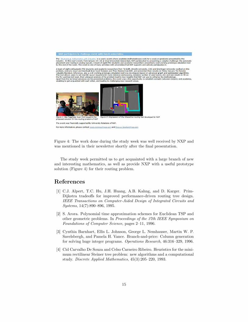
Figure 4: The work done during the study week was well received by NXP andwas mentioned in their newsletter shortly after the final presentation.
The study week permitted us to get acquainted with a large branch of newand interesting mathematics, as well as provide NXP with a useful prototypesolution (Figure 4) for their routing problem.
References
[1] C.J. Alpert, T.C. Hu, J.H. Huang, A.B. Kahng, and D. Karger. Prim-Dijkstra tradeoffs for improved performance-driven routing tree design.IEEE Transactions on Computer-Aided Design of Integrated Circuits andSystems, 14(7):890–896, 1995.
[2] S. Arora. Polynomial time approximation schemes for Euclidean TSP andother geometric problems. In Proceedings of the 37th IEEE Symposium onFoundations of Computer Science, pages 2–11, 1996.
[3] Cynthia Barnhart, Ellis L. Johnson, George L. Nemhauser, Martin W. P.Savelsbergh, and Pamela H. Vance. Branch-and-price: Column generationfor solving huge integer programs. Operations Research, 46:316–329, 1996.
[4] Cid Carvalho De Souza and Celso Carneiro Ribeiro. Heuristics for the mini-mum rectilinear Steiner tree problem: new algorithms and a computationalstudy. Discrete Applied Mathematics, 45(3):205–220, 1993.
15

[5] Guy Desaulniers, Jacques Desrosiers, and Marius M. Solomon, editors. Col-umn generation, volume 5 of GERAD 25th Anniversary Series. Springer,New York, 2005.
[6] E. W. Dijkstra. A note on two problems in connexion with graphs. Numer.Math., 1:269–271, 1959.
[7] M. R. Garey and D. S. Johnson. The Rectilinear Steiner Tree Problemis NP-Complete. SIAM Journal on Applied Mathematics, 32(4):826–834,1977.
[8] R. Geraerts. Planning short paths with clearance using explicit corridors. InIEEE International Conference on Robotics and Automation, pages 1997–2004, 2010.
[9] P. E. Hart, N. J. Nilsson, and B. Raphael. A Formal Basis for the HeuristicDetermination of Minimum Cost Paths. IEEE Transactions on SystemsScience and Cybernetics, 4(2):100–107, 1968.
[10] S. Held, B. Korte, D. Rautenbach, and J. Vygen. Combinatorial Optimiza-tion in VLSI design. In V. Chvatal and N. Sbihi, editors, CombinatorialOptimization: Methods and Applications. IOS Press, to appear.
[11] Renato F. Hentschke, Jaganathan Narasimham, Marcelo O. Johann, andRicardo L. Reis. Maze routing Steiner trees with effective critical sink opti-mization. In Proceedings of the 2007 international symposium on Physicaldesign, ISPD ’07, pages 135–142, New York, NY, USA, 2007. ACM.
[12] Huibo Hou, Jiang Hu, and S.S. Sapatnekar. Non-Hanan routing. IEEETransactions on Computer-Aided Design of Integrated Circuits and Sys-tems, 18(4):436–444, April 1999.
[13] Richard M. Karp. Reducibility among combinatorial problems. In Com-plexity of computer computations, pages 85–103. Plenum Press, New York,1972.
[14] Christine R. Leverenz and Miroslaw Truszczynski. The rectilinear Steinertree problem: algorithms and examples using permutations of the terminalset. In Proceedings of the 37th annual Southeast regional conference (CD-ROM), ACM-SE 37, New York, NY, USA, 1999. ACM.
[15] Chih-Hung Liu, Shih-Yi Yuan, Sy-Yen Kuo, and Szu-Chi Wang. High-performance obstacle-avoiding rectilinear Steiner tree construction. ACMTransactions on Design Automation of Electronic Systems, 14:45:1–45:29,2009.
[16] Dirk Muller, Klaus Radke, and Jens Vygen. Faster min–max resourcesharing in theory and practice. Mathematical Programming Computation,3:1–35, 2011. 10.1007/s12532-011-0023-y.
16
[17] S. Peyer, D. Rautenbach, and J. Vygen. A generalization of Dijkstra’sshortest path algorithm with applications to VLSI routing. Journal ofDiscrete Algorithms, 7:377–390, 2009.
[18] J. Scott Provan. An approximation scheme for finding Steiner trees withobstacles. SIAM J. Comput., 17(5):920–934, 1988.
[19] David Warme, Pawel Winter, and Martin Zachariasen. GeoSteiner [Com-puter Software]. www.diku.dk/hjemmesider/ansatte/martinz/geosteiner/.(version 3.1).
[20] Martin Zachariasen. Rectilinear full Steiner tree generation. Networks,33(2):125–143, 1999.
[21] Hai Zhou. Efficient Steiner tree construction based on spanning graphs. InProceedings of the 2003 international symposium on Physical design, ISPD’03, pages 152–157, New York, NY, USA, 2003. ACM.
17