design of high-speed cmos laser driver using...
TRANSCRIPT

DESIGN OF HIGH-SPEED CMOS LASER DRIVER USING A STANDARD CMOS TECHNOLOGY FOR OPTICAL
DATA TRANSMISSION
A Dissertation Presented to
The Academic Faculty
By
Seok Hun Hyun
In Partial Fulfillment Of the Requirements for the Degree
Doctor of Philosophy in the School of Electrical and Computer Engineering
School of Electrical and Computer Engineering Georgia Institute of Technology
Atlanta, GA 30332
November, 2004
Copyright © 2004 by Seok Hun Hyun
DESIGN OF HIGH-SPEED CMOS LASER DRIVER USING A STANDARD CMOS TECHNOLOGY FOR OPTICAL
DATA TRANSMISSION
Approved by:
Dr. Martin Brooke, Advisor Dr. Bernard Kippelen School of Electrical and Computer School of Electrical and Computer Engineering Engineering
Dr. David Schimmel Dr. Paul Kohl School of Electrical and Computer School of Chemical and Biomolecular Engineering Engineering
Dr. Paul Hasler Approval Date: November 18, 2004 School of Electrical and Computer Engineering

To my parents who are always believing in me. To my lovely wife, Soojung, who kept encouraging me
and my precious Youjin.

iv
ACKNOWLEDGEMENTS
First of all, I would like to thank my thesis advisor, Dr. Martin A. Brooke. This
work could not have been completed without his support, guidance, patience, and humor.
He is an outstanding researcher, mentor, and tremendous source of motivation. I will
always be grateful for his valuable advice and insight. A special Thank You goes to Dr.
Nan M. Jokerst helped and supported to complete this work. I would like to thank Dr.
David Schimmel, Dr. Paul Hasler, Dr. Bernard Kippelen, and Dr. Paul Kohl for serving
on my thesis committee. I would like to thank many fellow Ph.D. students aided in my
research and understanding. Finally, I have to thank to my family. Soojung has
contributed confidence and encouragement toward the completion of this works and she
always has been there for me, and my parents have been mentors for my life.
v
TABLE OF CONTENTS
ACKNOWLEDGEMENTS............................................................................................... iv
TABLE OF CONTENTS.....................................................................................................v
LIST OF TABLES........................................................................................................... viii
LIST OF FIGURES ........................................................................................................... ix
LIST OF ABBERRATIONS ........................................................................................... xiii
SUMMARY..................................................................................................................... xiv
CHAPTER I INTRODUCTION .................................................................................1
1.1 Dissertation Outlines....................................................................................4
CHAPTER II BACKGROUND ...................................................................................7
2.1 Comparison of Optical and Electrical Links................................................7
2.2 Optoelectronic Links..................................................................................12
2.3 Semiconductor Laser .................................................................................13
2.3.1 Modulation Bandwidth in Semiconductor Lasers..........................14
2.3.2 Turn-on delay.................................................................................16
2.3.3 Frequency Chirping .......................................................................17
2.3.4 Temperature Effects.......................................................................18
2.4 Laser Driver ...............................................................................................20
2.5 Evaluating System Performances ..............................................................24
2.5.1 Eye diagram ...................................................................................24
2.5.2 Eye pattern mask............................................................................26
2.5.3 Bit error rate (BER) measurements................................................27

vi
CHAPTER III DESIGN OF LOW POWER CMOS LASER DRIVER......................29
3.1 Introduction................................................................................................29
3.2 Design Considerations ...............................................................................31
3.3 Simulations ................................................................................................33
3.3.1 Schematic-based simulations .........................................................35
3.3.2 Layout-based simulations ..............................................................41
3.4 Experimental Results .................................................................................55
3.4.1 Test setup .......................................................................................55
3.4.2 Measurements ................................................................................60
CHAPTER IV THIN FILM LASER INTEGRATION ONTO CMOS CIRCUITS....65
4.1 Introduction................................................................................................65
4.2 Thin Film Laser..........................................................................................68
4.3 Simulations ................................................................................................75
4.4 Measurements ............................................................................................77
CHAPTER V DESIGN OF HIGH CURRENT LASER DRIVER FOR LVDS ........82
5.1 Introduction................................................................................................82
5.2 Bandwidth Enhancement Techniques........................................................83
5.2.1 Shunt Peaking Technique ..............................................................84
5.2.2 Source Degeneration......................................................................87
5.2.3 Cherry-Hooper Topology...............................................................88
5.3 Laser Driver for Edge-emitting Lasers ......................................................90
5.4 Simulations ................................................................................................96

vii
CHAPTER VI CONCLUSIONS AND FUTURE RESEARCH ...............................100
6.1 Contributions............................................................................................100
6.2 Future Research .......................................................................................103
6.3 Conclusions..............................................................................................104
APPENDIX HSPICE INPUT CONTROL FILES AND BSIM MODELS..................105
A.1 Low Power CMOS Laser Driver Input Control Files..............................105
A.2 High Current Laser Driver Input Control Files........................................110
A.3 Laser Driver Netlist File ..........................................................................111
A.4 TSMC 0.18 um Model Parameters ..........................................................130
REFERENCES ................................................................................................................134

viii
LISTS OF TABLES
Table 2-1 Relative merits of electrical and interconnection technologies [25].............11
Table 2-2 Basic SONET/SDH data rates [42]...............................................................26
Table 3-1 Predetermined design goals of the laser driver .............................................31
Table 3-2 Optimized bias conditions and specifications of the laser driver .................61
Table 4-1 Thin film laser material structure..................................................................69
Table 5-1 Design goals for high-current laser driver ....................................................91
Table 5-2 Specified circuit performances .....................................................................98
Table 6-1 The performance comparison of the laser driver in this research with recently published.......................................................................................102
Table 6-2 The comparison of proposed laser driver and Peterson’s laser driver ........102

ix
LISTS OF FIGURES
Figure 2.1 Illustration of electrical interconnection lines.................................................9
Figure 2.2 Simple block diagram of optoelectronic links ..............................................12
Figure 2.3 The L-I curve for laser and LED. Ith indicates the threshold current of the laser ...............................................................................................................14
Figure 2.4 Output power vs. Frequency. τf is the relaxation oscillation frequency .....16
Figure 2.5 Effect of variable delay in lasers...................................................................17
Figure 2.6 Temperature effects on semiconductor lasers...............................................19
Figure 2.7 Modulation scheme: (a) Direct modulation and (b) External modulation....21
Figure 2.8 Schematic of simple laser drivers .................................................................23
Figure 2.9 Various bit sequences and corresponding eye diagram ................................25
Figure 2.10 The characteristics of an eye diagram...........................................................25
Figure 2.11 Mask of the eye diagram for the optical transmit signal [43] .......................28
Figure 2.12 Typical BER characterization at high-speed [40].........................................28
Figure 3.1 Schematics of laser drivers ...........................................................................32
Figure 3.2 The flowchart of the simulation processes....................................................34
Figure 3.3 Simulated transient response of laser driver design at 10 Gbps with on chip parasitics only ..............................................................................................36
Figure 3.4 (a) A simplified supply-independent voltage reference circuit. (b) The implementation of a voltage reference circuit ..............................................38
Figure 3.5 Simulation results of the voltage reference circuit. (a) represents the Vref and (b) represents the change of the Vgs1 and Vgs2. As the value of Vgs1 is increased, the Vgs2 is decreased, resulting in a compensated reference voltage...........................................................................................................38
Figure 3.6 The equivalent circuits of a laser diode and parameters fitting for bias information....................................................................................................40
x
Figure 3.7 Comparisons of layout-based simulation and schematic simulations. The top trace represents the schematic simulation. The second trace represents the layout-based simulations. The last trace indicates the 50 ohm load laser driver instead of a laser mode .......................................................................42
Figure 3.8 Differential switch divided into two parts to make a symmetrical layout along the signal path .....................................................................................44
Figure 3.9 Block diagram of ESD circuitry ...................................................................45
Figure 3.10 The layout of designed laser driver circuits..................................................46
Figure 3.11 The layout out of whole chip, which includes laser driver, transimpedance amplifier. The empty space in the middle of the chip is for a laser and a detector integration site.................................................................................46
Figure 3.12 Simplified circuit schematic: The circuit model includes the parasitic inductance, Lcable on cable, Ltrace of the power line on the PCB, and Lbonding
on wire bonding ............................................................................................48
Figure 3.13 Transient simulation with line parasitics and no decoupling capacitors. The top trace represents the output current of laser diode, the second trace shows the eye diagram of the laser driver, and the last trace represents the voltage fluctuation in the power supply rails.............................................................50
Figure 3.14 Equivalent circuit model of capacitor ...........................................................50
Figure 3.15 (a) Equivalent circuit of MiM capacitor. (b) the MiM capacitor simulated s-parameters, S21 (top) shows broad coupling and S11 (bottom) shows the resonance frequency of the capacitor............................................................52
Figure 3.16 Frequency response of the laser driver without decoupling capacitors ........52
Figure 3.17 Frequency response of the laser driver with decoupling capacitors .............53
Figure 3.18 Transient simulation with MiM capacitors and line parasitics at 10 Gbps. The top trace represents the output current of laser diode, the second trace shows the eye diagram of the laser drivers, and the last trace represents the output voltage fluctuations in power supply rails.........................................54
Figure 3.19 The eye diagram of laser driver at 10 Gbps with the temperature variations. The yellow line is at 27 °C, the red line is at 100 °C, and the cyan line is at 200 °C ...........................................................................................................55
Figure 3.20 Block diagram of test setup...........................................................................56
Figure 3.21 Layout of test board of the laser driver.........................................................57

xi
Figure 3.22 Momentum simulations of the FR4 test board with HPADS .......................58
Figure 3.23 Transmission characteristics of the traces on the test board .........................58
Figure 3.24 Picture of test board ......................................................................................59
Figure 3.25 A microphotograph of the wire-bonded laser driver.....................................59
Figure 3.26 Measured eye diagram at 1 Gbps..................................................................61
Figure 3.27 Measured eye diagram at 5 Gbps..................................................................62
Figure 3.28 Electrically measured output data stream at 10 Gbps...................................62
Figure 3.29 Electrically measured eye diagram at 10 Gbps.............................................63
Figure 3.30 Eye diagram with SONET OC-192 eye mask ..............................................63
Figure 3.31 Electrical measured eye diagram at 12 Gbps................................................64
Figure 4.1 L-I measurement: the thin film laser on BCB coated silicon wafer. The measured threshold current is approximately 25 mA when the injected current has 10 % of the duty cycle................................................................70
Figure 4.2 V-I measurement: the thin film laser on BCB coated silicon wafer .............70
Figure 4.3 Pulsed-mode s-parameter measurement setup ..............................................71
Figure 4.4 Performance comparison between pulsed-mode and CW mode operations.72
Figure 4.5 Test setup for pulsed-mode laser driver........................................................73
Figure 4.6 The output shows the pulsed-mode operation of the laser driver at the oscilloscope. Top window represents law data captured at the output of the circuit. The second and third windows are zoomed data..............................74
Figure 4.7 The eye diagram out of the pulsed data output .............................................74
Figure 4.8 The comparison of the transfer characteristics (S21) of the transmission line between measurement and simulation ..........................................................76
Figure 4.9 The transfer characteristics of transmission lines on silicon substrate with and without SiO2 coatings ............................................................................76
Figure 4.10 Transient response of thin film laser.............................................................77
Figure 4.11 A microphotograph of the integrated thin film laser onto CMOS circuit.....78
Figure 4.12 Thin film laser integration process ...............................................................80

xii
Figure 4.13 Circuit photo with wirebonding diagram......................................................80
Figure 4.14 Integrated circuit photo with wirebonds .......................................................81
Figure 4.15 L-I measurement of the thin film laser on CMOS circuitry. The pulsed current was applied to minimize the thermal problem of the thin
film laser .......................................................................................................81
Figure 5.1 (a) Typical attenuation versus wavelength plot for a silica-based optical fiber [67, 68] (b) Typical single mode fiber dispersion vs. wavelength
curve..............................................................................................................83
Figure 5.2 Schematics of common source (CS) amplifier with and without shunt peaking..........................................................................................................85
Figure 5.3 Frequency response of CS amplifier and shunt peaking...............................86
Figure 5.4 (a) Schematic of simplified active inductor. (b) Small-signal equivalent circuit ............................................................................................................87
Figure 5.5 (a) Differential pair with capacitive degeneration. (b) Small-signal model with half circuit.............................................................................................88
Figure 5.6 (a) Standard form of Cherry-Hooper amplifier. (b) Small-signal half circuit ............................................................................................................90
Figure 5.7 Schematics of pre-driver stage with (a) modified Cherry-Hooper amplifier. (b) Shunt peaking with active inductors .......................................................93
Figure 5.8 Schematic of high current laser driver with the modified Cherry-Hooper amplifier........................................................................................................94
Figure 5.9 Schematic of high current laser driver with shunt peaking with active inductors........................................................................................................95
Figure 5.10 Frequency response of the pre-drivers. The blue line represents the shunt peaking amplifier and the red one represents the modified Cherry-Hooper amplifier........................................................................................................96
Figure 5.11 Transient response of high-current laser driver using the modified Cherry-Hooper amplifier at 10 Gbps ........................................................................98
Figure 5.12 Transient response of high-current laser driver using the shunt peaking with active inductors .............................................................................................99

xiii
LIST OF ABBREVIATIONS
BER Bit error rate BERT Bit error rate tester BPS Bit per second CH Cherry-Hooper CMOS Complementary metal oxide silicon COB Chip-on-board CS Current switch CW Continuous wave DFB Distributed feedback DH Double heterojunction ELO Epitaxial liftoff ESD Electrostatic discharge FP Febry-Perrot FTTX Fiber-to-the-curb/home/building/desktop GaAs Gallium arsenide InP Indium phosphide ISI Intersymbol interference LAN Local area network LED light emitting diode LVDS Low voltage differential signal MIM Metal-Insulator-Metal MQW Multiquantum well NA Numerical aperture NRZ Non return to zero OOK On-off keying PCB Printed Circuit Board PRBS Pseudo random bit sequence SDH Synchronous digital hierarchy SiO2 Silicon dioxide SMU Source measurement unit SONET Synchronous optical networks TSMC Twain semiconductor manufacturing service VCSEL Vertical cavity surface emitting laser WAN Metropolitan area network WMD Wavelength division multiplexing
xiv
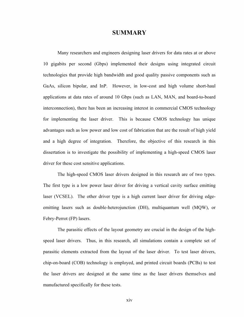
SUMMARY
Many researchers and engineers designing laser drivers for data rates at or above
10 gigabits per second (Gbps) implemented their designs using integrated circuit
technologies that provide high bandwidth and good quality passive components such as
GaAs, silicon bipolar, and InP. However, in low-cost and high volume short-haul
applications at data rates of around 10 Gbps (such as LAN, MAN, and board-to-board
interconnection), there has been an increasing interest in commercial CMOS technology
for implementing the laser driver. This is because CMOS technology has unique
advantages such as low power and low cost of fabrication that are the result of high yield
and a high degree of integration. Therefore, the objective of this research in this
dissertation is to investigate the possibility of implementing a high-speed CMOS laser
driver for these cost sensitive applications.
The high-speed CMOS laser drivers designed in this research are of two types.
The first type is a low power laser driver for driving a vertical cavity surface emitting
laser (VCSEL). The other driver type is a high current laser driver for driving edge-
emitting lasers such as double-heterojunction (DH), multiquantum well (MQW), or
Febry-Perrot (FP) lasers.
The parasitic effects of the layout geometry are crucial in the design of the high-
speed laser drivers. Thus, in this research, all simulations contain a complete set of
parasitic elements extracted from the layout of the laser driver. To test laser drivers,
chip-on-board (COB) technology is employed, and printed circuit boards (PCBs) to test
the laser drivers are designed at the same time as the laser drivers themselves and
manufactured specifically for these tests.

xv
This research makes two significant new contributions to the technology that are
reported and described here. One is the first 10 Gbps performance of a differential
CMOS laser driver with better than 10-14 bit-error-rate (BER). The second is the first
demonstration of a heterogeneous integration method to integrate independently grown
and customized thin film lasers onto CMOS laser driver circuits to form an optical
transmitter.

1
CHAPTER I
INTRODUCTION
As the technology of communication systems has advanced in modern society, the
amount of information transported has increased enormously. The technology of first the
electronic era and then the microelectronic era led to the development of a profusion of
analog and digital communication techniques that resulted in the installation and
expansion of wireless and satellite links. Repeatedly scientists and engineers have found
ways to exploit the available bandwidth and to expand its capacity for information to the
point where fundamental constraints of noise, interference, power, cost, and other issues
began to limit progress in electronic communication links. Research in how to surmount
these limitations brought the next step in the evolution of communication systems, which
is the use of optics as a replacement for electronics. The inherent advantages of optics, as
compared with conventional electronics, have led a widespread replacement of copper
wires for communication at data rates above Mbps and over kilometers. For example,
wide bandwidth optical fibers allow high data rates and large data capacity with low
transmission loss, which allows vastly increased distances between repeaters. In addition,
a natural immunity to RF electromagnetic interference helps keep signal noise ratios low
and permits the use of optical communication systems in noisy environments. As a
consequence of these advantages, optical systems have replaced conventional electronic
communication systems in long-distance applications and gradually are coming into use
in networks involving shorter distances.

2
Today optical communication systems are used in many applications such as
synchronous digital hierarchy (SDH)/synchronous optical networks, (SONET) systems,
wavelength division multiplexing (WMD) network systems, Local Area Networks
(LANs), Metropolitan Area Networks (MANs), fiber-to-the-curb/home/building/desktop
(FTTX), and board-to-board interconnections, all of which use optical fiber for data
conveyance [1].
A typical optical communication system has three main components: a transmitter,
a transmission medium, and a receiver. This basic structure of the system resembles
conventional electronic communication systems. The difference is that optical
communications use optical signals as a carrier of information instead of using electronic
pulses to transmit information through copper wires. The transmitter is composed of
optical sources such as a laser or a light emitting diode (LED) and driver circuits.
Semiconductor lasers are currently the main light output source in high-speed
applications. The laser driver circuit is one of the key components because it performs as
the interface between the electronic devices and the optical devices and, as such, affects
the performance of the entire optical communication system. Its design, although simple
in concept, is very challenging because of the difficulty of determining specifications that
accommodate both large output current and operation at high-speed. To determine these
design constraints a general understanding of the system into which the laser driver
integrates is necessary.
Many researchers and engineers designing laser drivers for data rates at or above
10 gigabits per second (Gbps) implemented their designs using integrated circuit
technologies that provide high bandwidth and good quality passive components such as

3
GaAs [2-8], silicon bipolar [1, 9], and InP [10-12]. However, in low-cost and high
volume short-haul applications at data rates of around 10 Gbps (such as LAN, MAN,
FTTX, and board-to-board interconnection) there has been an increasing interest in
commercial CMOS technology for implementing the laser driver. This is because CMOS
technology has unique advantages such as low power and low cost of fabrication that are
the result of high yield and a high degree of integration. Therefore, the objective of this
research in this dissertation is to investigate the possibility of implementing a high-speed
CMOS laser driver for these cost sensitive applications.
The high-speed CMOS laser drivers designed in this research are of two types.
The first type is a low power laser driver for driving a vertical cavity surface emitting
laser (VCSEL). This laser driver must deliver a maximum of 10 mAp-p modulation
current and 10 mA bias current.
The other driver type is a high current laser driver for driving edge-emitting lasers
such as double-heterojunction (DH), multiquantum well (MQW), or Febry-Perrot (FP)
lasers. This type of laser driver requires larger currents to drive the lasers: for example,
the modulation currents need to be above 20 mAp-p and bias currents of more than 20 mA
are needed.
The parasitic effects of the layout geometry are crucial in the design of the high-
speed laser drivers. Thus, in this research, all simulations contain a complete set of
parasitic elements extracted from the layout of the laser driver. To test laser drivers,
chip-on-board (COB) technology is employed, and printed circuit boards (PCBs) to test
the laser drivers are designed at the same time as the laser drivers themselves and
manufactured specifically for these tests. This research makes two significant new

4
contributions to the technology that are reported and described here. One is the first 10
Gbps performance of a differential CMOS laser driver with better than 10-14 bit-error-rate
(BER). The second is the first demonstration of a heterogeneous integration method to
integrate independently grown and customized thin film lasers onto CMOS laser driver
circuits to form an optical transmitter.
1.1 Dissertation Outline
This dissertation presents the results of designs and experimental study of high-
speed CMOS laser drivers for short-haul applications. The first part (Chapters III and
IV) of this dissertation is dedicated to the design, layout, and measurements of a low
power and high-speed laser driver. The second part (Chapter V) presents the design of a
high current laser driver with low voltage differential signal (LVDS) input stages. A
brief chapter-to-chapter outline of the dissertation is given below.
Chapter II provides background information on laser driver design. It starts with
a discussion of the comparison of optical interconnects and electrical interconnects to
provide the motivation of the research. Also covered in this chapter are a review of
optical communication systems and descriptions of each component in the system. In
addition, a brief comparison between lasers and LEDs as optical source is presented.
Also included in this chapter is a basic concept of laser drivers. This section gives a brief
review of modulation schemes, external and direct modulation. Some examples of laser
drivers are also covered, along with an analysis of their comparative advantages and
disadvantages. The last section of Chapter II describes the criteria, such as eye-diagram
and BER test, for evaluating system performance of laser drivers.
5
Chapter III covers the design and implementation of a low power and high-speed
CMOS laser driver. In the first section, design considerations are presented with the
simulation process. The equivalent laser model provided by a corporate research partner
and modified for this research is explained. Because the parasitic effects play a
significant role in the implementation of a high-speed laser driver, the layout
considerations are covered. To solve those parasitics effects on laser drivers, a
decoupling technique using metal-insulator-metal (MIM) capacitors is employed. A test
setup and some measurements results of the laser driver also are included in the chapter.
Chapter IV describes the optical transmitter, which consists of the laser driver and
a thin film laser. The first section of this chapter covers the integration techniques used
to form an optical transmitter. More established hybrid integration techniques such as
flip-chip and epitaxial liftoff (ELO) are discussed. The fabrication of the thin film laser
and some measurements results are also included. At the time of this writing, the thin
film laser independently developed and optimized at Georgia Tech has thermal problems
that require a pulsed mode testing setup. Therefore, the pulsed mode setup and
experimental results are shown in this chapter. Using a transfer diaphragm
heterogeneous integration process, a thin film laser is integrated onto a silicon CMOS
laser driver, and the results of measurements are included in this chapter.
Chapter V describes the high-output current laser driver for driving edge-emitting
lasers. This laser driver is compatible with the IEEE standard for low-voltage differential
signals. To obtain high gain, modified Cherry-Hooper amplifier stages are included as a
pre-driver stage. In addition, the bandwidth enhancement techniques used in CMOS
technology are discussed in this chapter.

6
The final chapter summarizes the goal of this research and the contributions made
to the field. It also points out how this research can be extended into the future.

7
CHAPTER II
BACKGROUND
This chapter presents basic concepts necessary for a better understanding of
optical laser drivers. The first section compares optical and electrical links as a way to
explain the advantages of the optical links. The second section then explains the basic
concept of optical links as well as each component that makes up optical links. The next
section examines laser driver circuits and the characteristics of the laser diode that are
used in them. Finally, methods such as eye-diagram and BER test that are used to
evaluate the system performances are explained.
2.1 Comparison of Optical and Electrical Links
The ongoing multimedia trend and the amount of communication required in the
modern information and knowledge society imposes enormous performance requirements
on computer networks and on the electronic equipment itself. In turn, these demands
force the semiconductor industry to develop and manufacture even more powerful and
faster components, especially microprocessors operating with clock frequencies of more
than 3 GHz [13]. In addition, the continuing exponential reduction in feature sizes on
electronic chips, known as Moore’s law [2], results in large numbers of faster devices at
lower cost. However, this advance alters the balance between devices and
interconnections in systems; electrical interconnections do not scale proportionally with
the devices. Consequently, these high-speed devices and components cannot deliver their

8
optimal performances because of the technical deficiency of interconnections. For
example, the buses inside computer systems that carry the information from one part of
the system to another run much slower than the clock rate on the core chips because of
the various problems in the electrical interconnections. Moreover, the performance of
many digital systems is limited by the bandwidth of the electrical interconnections that
use printed circuit boards (PCB) and a multichip module between the chips and boards.
Hence, the system has a bandwidth limitation that is imposed by the length of the
interconnection line rather than by the performance of the semiconductor technology.
Problems associated with scaling create one of the most critical limitations in
electrical interconnection technology. If simple electrical interconnections are considered,
as shown in Figure 2.1, and scaled down with a scaling factor α, then the thickness (Hint),
the width (Wint), the space between wires (Wsp), and the length (Lint) could shrink by 1/α.
The conductor cross section area would shrink 1/α2, increasing the resistance per unit
length accordingly to α2, shown in equation (2.1.1). The National Technology Roadmap
for Semiconductors (NTRS) [14] uses a nominal value of 2=α for generation to
generation scaling, or 1/α=0.707.
2intint1α=× HW , 2
intintintint
1 αρ =×
⋅=HW
R (2.1.1)
where ρint is the resistivity of materials. The capacitance per unit length does not change
in such a shrinking-it depends only on the geometry of the line, not its size. The length of
the interconnection line has been shrunk to 1/α, and so the total RC delay is RintCintL2int =1.
This means that the RC time constant cannot be reduced by the scaling factor but has to
be reduced for global interconnections.

9
With increasing levels of integration, the die size will increase and require fatter
wires in the chip. This will increase cross talk and decrease the yield of the die. The
transistors on a chip get faster as the technology dimension shrinks, but the electrical
interconnections are not keeping up with the transistors. Obviously, the electrical
interconnections do rely on wires with their associated inductance, resistance, and
capacitance. Hence, problems in the electrical interconnections included in scaling are
relevant to the physics of wires and hardly avoidable in principle.
W sp
L int
int WHint
Figure 2.1. Illustration of electrical interconnection lines.
Because these problems are inherent in the physics of wires, there has been
significant interest in using optics for interconnection technology as a way to solve many
physical problems such as signal and clock distortion, skew and attenuation, impedance
mismatching, cross-talk, power dissipation, wave reflection phenomena, and interconnect
density limitations [15]. Historically, optical interconnections have been successfully

10
implemented and have replaced electrical interconnections in long-distance applications
in which relatively few optoelectronic interfaces are necessary. Moreover, electrical
interconnections gradually are being replaced in short-distance communications such as
in chip-to-chip interconnections.
Ever since optics began to be used in interconnection technology, many
researchers have compared them with conventional electrical interconnections and
discussed their potential [16-19]. In general, there exists a critical length above which
optical interconnects are preferred from the point of view of performance, power
dissipation, and a speed. Although the critical length varies with different technical
assumptions, the trend away from electrical interconnections and to optical
interconnections is clear and is becoming apparent in short-distance applications. A list
of the advantages most often cited for optical interconnection technologies is presented in
Table 2-1.
Recently a lot of research has been concentrated on developing optical chip-to-
chip interconnections. The board, backplane [20], chip level 3-D stacking for free space
[21], and plastic optical fiber-based (POF) interconnection [22, 23] all have been
demonstrated. Also, cost-effective solutions for optoelectronic interconnects with CMOS
circuitry were presented in [24].

11
Table 2-1. Relative merits of electrical and interconnection technologies [25].
Electrical Optical
• High-Power Line-Driver Requirements • Higher interconnection densities
• Thermal Management Problems • Higher packing densities of gates on integrated circuit chips
• Signal Distortion • Lower power dissipation and easier
thermal management of systems that require high data rates
• Dispersion: Interconnection delay varies with frequency
• Less signal dispersion than comparable electronic scheme
• Attenuation: signal attenuation that varies with frequency
• Easier impedance matching of transmission lines
• Crosstalk: capacitive and inductive coupling from signals on neighboring traces
• Less signal distortion
• Reflection/Ringing: impedance matching requirements not met • Greater immunity to EMI
• Signal Skew: variations in the delay between different waveforms on different paths in signal and clock traces
• Lower signal and clock-skew
• High-Sensitivity to Electromagnetic Interference (EMI)

12
2.2 Optoelectronic Links
The system block diagram for optoelectronic links is shown in Figure 2.2. It
consists of an optical transmitter, optical source, optical medium, photodetector, and
optical receiver. On the transmitting side, the optical transmitter converts the input signal
from the optical source into a large current used to modulate the optical source. The light
output propagates through the optical medium in which optical fiber, free space, or
waveguide is commonly included. The light signal from the optical medium is collected
by a photodetector that generates an electrical current. The optical receiver uses the
photodetector to convert the optical signal into an electrical signal and amplifies it
enough to be treated as a digital signal. It is the cost and efficiency of these processes
that will determine whether such links are consider for on-chip and chip-to-chip
communication.
Photodetector
Optical MediumOptical Transmitter Optical Receiver
Laser Diode
LaserDriver Transimpdeance
Amplifier
Figure 2.2. Simple block diagram of optoelectronic links.

13
Although the system topology shown in Figure 2.2 has changed little over the past
several decades, the design of its building blocks and the levels of integration have.
Driven by the evolution and affordability of IC technologies as well as by the demand for
higher performance, this change has created new challenges that require new circuit and
architecture techniques [26].
2.3 Semiconductor Laser
The main optical source in communication system is either light-emitting diodes
(LEDs) or semiconductor lasers. The advantages of the laser over the LED, such as its
unique size, spectral region of operation, high efficiency, and high-speed operation have
led to dramatic improvements in high-speed optical communication systems. In the early
stages of semiconductor laser development the trend was toward optimizing laser
structures for improvements in static lasing characteristics in terms of threshold current,
quantum efficiency, linearity of light versus current characteristic, operation at high
optical power, and long-term reliability [27]. As laser fabrication technology improved,
the high-speed dynamic characteristics of lasers become increasingly important. A plot
of the light output power from a semiconductor laser and LED is shown in Figure 2.3.
If the current is less than a threshold value, Ith, the optical power of the laser is
small, and the device operates as an LED, using spontaneous emission. As the current
increases above the threshold value, the stimulated emission becomes dominant and the
laser begins operating in the linear region with high slope efficiency (dL/dI) compared
with the LED.

14
OutputPower
(L)
IthInput current (I)
Laser
LEDSpontaneousEmission
StimulatedEmission
Figure 2.3. The L-I curve for laser and LED. Ith indicates the threshold current of the laser.
2.3.1 Modulation Bandwidth in Semiconductor Lasers
One of the most interesting characteristics of lasers in optical communication
systems is the maximum modulation speed of the laser. The small-signal response of the
laser is obtained by linearizing the rate equations. The resulting dynamic solution for
small-signal modulation is a second-order transfer function [28].
( )
++
−+
+=
∆∆
osp
sosp
so
PjP
PJP
στ
ωωτβστ
τβ
11 2
(2.3.1)
where P is the photon density in a mode of the laser cavity, sσ is a collection of constants
describing the strength of the optical interaction; sτ is the spontaneous recombination life
time of the carriers; pτ is the photon life time, which is the average time a photon stays
in the cavity; oP is the steady-state photon density; andβ is the fraction of spontaneous
15
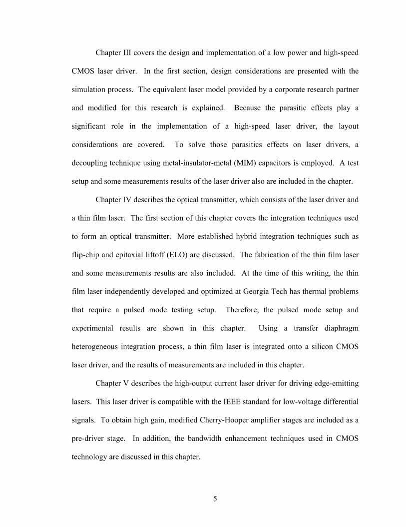
emission entering the lasing mode. At large frequencies, the 2ω term in the denominator
dominates and the small signal response of laser falls off rapidly with a frequency above
a critical value [27, 28]. The critical frequency for modulation is when the denominator
is minimized,
( )qV
IIgPf thiog
p
os −Γ=≈
ηυτσ
πτ 21 (2.3.2)
where iη is the internal quantum efficiency;Γ is the optical confinement factor; gυ is the
group velocity of optical mode; q is the electron charge; V is the active region volume;
( )thII − is the bias current above threshold; and og is the differential gain [29].
The modulation bandwidth of the laser is accepted as equal to τf . As illustrated
in Figure 2.4, the output power by current modulation is a flat function at low frequency,
but shows a peaking at near τf . Resonance in the modulation response, known in a laser
as the relaxation oscillation [27], physically results from coupling between the intensity
and the population inversion via stimulated emission. Such oscillation causes distortion
(ringing) in the shape of the output light pulse that requires some time to settle. Thus,
this oscillation limits the speed of the laser.
Equation (2.3.2) suggests three ways to increase the modulation bandwidth of
laser. One is by increasing the optical gain coefficient sσ , a second is by increasing
photon density Po, and the third is by decreasing the photon lifetime pτ .

16
f τ Frequency
Power
Figure 2.4. Output power vs. Frequency. τf is the relaxation oscillation frequency.
The gain coefficient can be increased roughly by a factor of five by cooling the
laser from room temperature to 77 oK [27]. To increase photon density, the cavity of the
laser should have higher reflectivity, which results in a smaller threshold current. The
third way to increase the modulation bandwidth is to reduce the length of laser cavity.
However, the maximum frequency only increases by the square root of changes in the
power of the photon lifetime, so it is not easy to make dramatic improvement in the
frequency response.
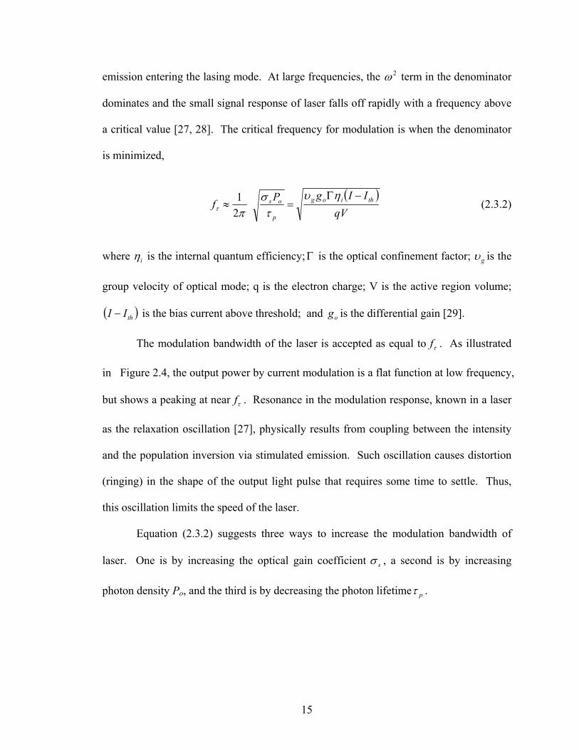
2.3.2 Turn-on delay
When a laser is turned on, photon generation begins as a spontaneous emission
until the carrier density exceeds a threshold level. Thus, stimulated emission occurs after
some delay. This turn-on delay is illustrated in Figure 2.5 and causes the jitters in the
output. For an applied current pulse of amplitude of Ip the turn-on delay is given by [30]
17
−+=
thbp
pthd III
Iττ (2.3.3)
where Ib is a bias current, Ith is the threshold current, and thτ is the delay at threshold.
Equation (2.3.3) implies that the turn-on delay will be reduced by the use of a large
modulation current and a low threshold current laser. Therefore, for a fast switching
operation, common practice is to bias the laser diode slightly above the threshold to avoid
turn-on delay.
tt δt
Iin
Pout
δ
Figure 2.5. Effect of variable delay in lasers.
2.3.3 Frequency Chirping
As pulses get shorter with an increase in the bit rate, chromatic dispersion, the
change of the index of refraction with wavelength, becomes important and plays a
significant role in limiting the performance of optical communication systems. When the
current through the laser is modulated, the laser wavelength is also modulated with the

18
power output from the laser. This effect is called frequency chirping. The principal
consequence of chirping is the broadening of the light spectrum, leading to substantial
dispersion in optical fibers carrying such signals, thereby creating intersymbol
interference (ISI) [26]. This spectrum broadening coupled with the dispersive properties
of optical fibers limits the maximum fiber transmission distance at high frequency. An
approximate equation for chirping is given as:
( )
+=∆ )()(
)(1
4tP
dttdP
tPt κ
παν (2.3.4)
where κ =2 hvV dηεΓ , dη is the differential quantum efficiency, h is a Planck’s constant,
ν is the optical frequency, α is the linewidth enhancement factor [31], and ε is the
nonlinear gain coefficient. The equation (2.3.4) implies the frequency shift ( )tν∆ is
proportional to the rate of change of the optical output power dP(t)/dt [29].
2.3.4 Temperature effects
A laser does not maintain a constant optical output if the temperature of device
changes. As shown in Figure 2.6, the threshold current can be expressed approximately
in terms of the working temperature such as:
TiT
th eKITI 10)( += (2.3.5)
in which I0, K1, and Ti are laser-specific constants. Example constants for a DFB laser
are I0=1.8mA, K1=3.85mA, and Ti=40oC [32].

19
Slope efficiency (S) is defined as the ratio of the optical output power to the input
current. As the temperature is increased, slope efficiency is decreased. The following
equation provides an estimation of slope efficiency as a function of temperature:
STT
So eKSTS −=)( (2.3.6)
For the same DFB laser in the above example, the characteristic temperature, Ts,
is close to 40 oC, So=0.485mW/mA, and Ks= 0.033mW/mA [32].
Figure 2.6. Temperature effects on semiconductor lasers.
20
2.4 Laser Driver
A laser driver can be considered a simple current switch that responds to an input
signal modulated by the data stream. As shown in Figure 2.3, the light output from a
laser is defined as a function of the input current rather than of voltage. If the
temperature of the laser is changed, large current fluctuations can result, even if the
voltage is held constant. Similarly, very small fluctuations in drive voltage would
correspond to dramatic changes in current and output power. For this reason, and
because of the speed advantages of current switching, laser diodes are driven by currents.
In general, in most optical systems, the electro-optic interface limits the maximum
speed of the system. Therefore, laser drivers and optical receivers are very important
components that determine the performance of optical systems. It is imperative that the
laser driver be able to function reliably at high speed as an optical signal generator. One
of the critical challenges of the laser driver is to deliver tens of milliamperes of current
with very short rise and fall times because bandwidth is a trade-off for large output
current.
Optical transmitter circuitry falls into two categories that are defined by methods
of modulation. One is the directly modulated transmitter consisting of a laser diode and a
laser driver. This type has been used in long- and short-haul transmission systems. As
shown in Figure 2.7 (a), the input data stream is directly modulated by the laser driver,
and the laser diode emits light output in response to the logic of “one” or “zero”.
Although a variety of modulation schemes have been attempted, the simplest and most
widely used modulation scheme is the direct modulation of the light intensity by data,
called on-off keying (OOK).
21
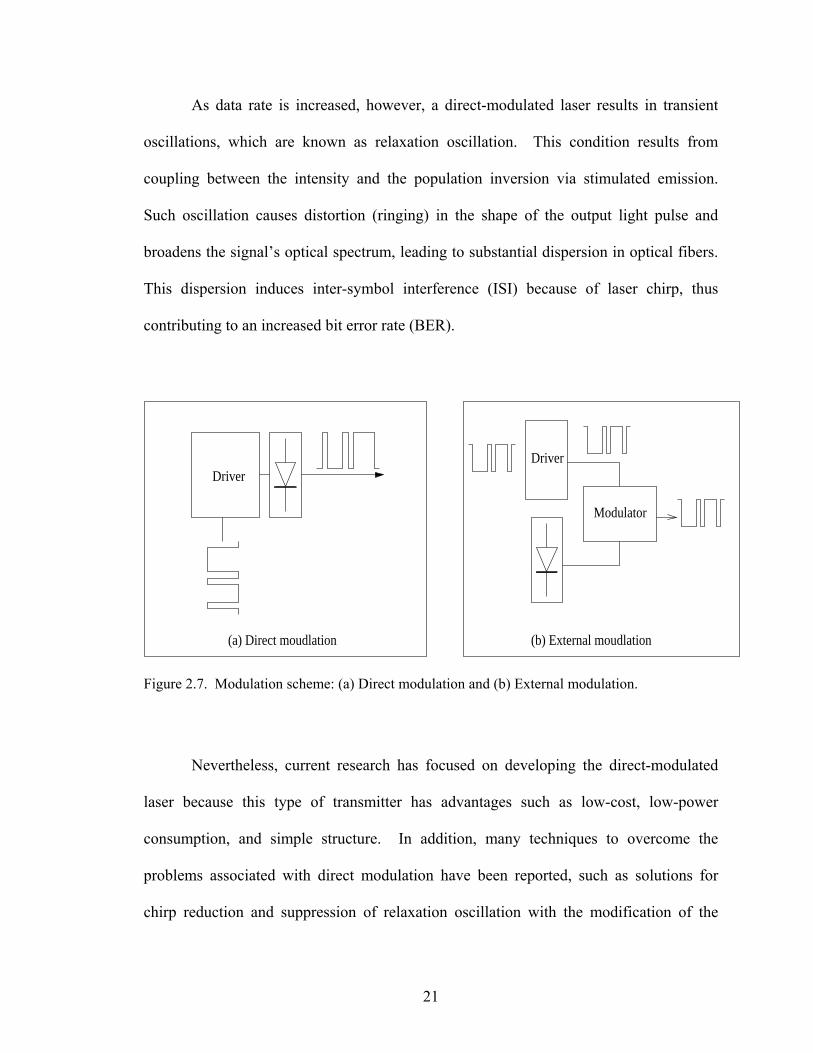
As data rate is increased, however, a direct-modulated laser results in transient
oscillations, which are known as relaxation oscillation. This condition results from
coupling between the intensity and the population inversion via stimulated emission.
Such oscillation causes distortion (ringing) in the shape of the output light pulse and
broadens the signal’s optical spectrum, leading to substantial dispersion in optical fibers.
This dispersion induces inter-symbol interference (ISI) because of laser chirp, thus
contributing to an increased bit error rate (BER).
(a) Direct moudlation
DriverDriver
Modulator
(b) External moudlation
Figure 2.7. Modulation scheme: (a) Direct modulation and (b) External modulation.
Nevertheless, current research has focused on developing the direct-modulated
laser because this type of transmitter has advantages such as low-cost, low-power
consumption, and simple structure. In addition, many techniques to overcome the
problems associated with direct modulation have been reported, such as solutions for
chirp reduction and suppression of relaxation oscillation with the modification of the
22
physical laser devices [27, 33-35]. Consequently, for a 10 Gbps short-distance system,
much effort has been devoted to a directly modulated transmitter.
The other type of optical transmitter is externally modulated and consists of a
laser driver, a laser diode, and an external modulator, which can achieve a lower chirp, or
even a negative chirp, to support the dispersion in the fiber [36]. External modulation
can have higher link gain and lower link noise but it needs a higher-power laser, high
electrical input power and it is more expensive. In this modulation scheme, shown in
Figure 2.7 (b), the laser is maintained in a constant light-emitting state and the external
modulator modulates the output intensity according to an externally applied voltage.
Mach-Zehnder type electro-optic modulators fabricated in either lithium niobate or
gallium arsenide are often used for this purpose.
Typically, the design of laser driver circuits incorporates the use of various
feedback loops to compensate for the effects of variations of the input data stream and for
temperature and aging. One simple laser driver circuit used to connect the output of a
current driver circuit directly to the laser diode is shown in Figure 2.8 (a) [37]. The
threshold current for a laser is provided by Vb, and the modulation current is provided by
a source resistor, Rmod, respectively. This type of single-ended laser driver is typically
used with low operating speed because of the unwanted parasitic inductance from the
package’s bonding wires, L1. When this parasitic inductance is combined with the high
impedance of the laser driver circuits and the low impedance of the lasers, it degrades the
output of the laser’s rise time and causes a power supply current ripple.
The laser driver shown in Figure 2.8 (b) [38] makes use of open collector
topology. The laser is connected directly to the collector of one transistor of a differential

23
pair with the bias current supplied by the current source, Imod. The laser current is the
sum of the collector currents of Q2 and Idc. Whenever light output is called for, these
currents can be controlled to exceed threshold and reach a point substantially up the
lasing region of the L-I curve. Matching circuitry between the driver and the laser must
be used to overcome the large impedance mismatch that occurs in this topology.
Vdd
Laser
(a) (b)
Q1 Q2M1
Vdd
Vss
Vss
Laser
L1
Rmod
Idc
VssVss
VrefImod
Vb
−
+
Figure 2.8. Schematic of simple laser drivers.
As data rates and transmission distances increase, the output of the laser diode
needs to be more precisely controlled. Because the laser’s output power can vary with
temperature and over its lifetime, higher performance system incorporate some method of
monitoring the light output and providing feedback of this information to the driver [39].

24
2.5 Evaluating System Performances
2.5.1 Eye diagram
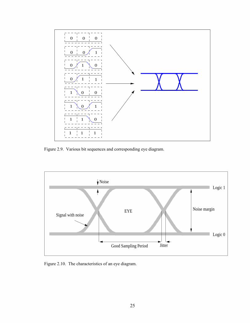
The eye diagram is, as shown in Figure 2.9, an overlay of many transmitted
waveforms whose shape resembles a human eye. By using a clock signal as the trigger
input to the oscilloscope, the transmitted waveform can be sampled over virtually the
entire data pattern generated by the transmitter. Thus, all the various bit sequences that
might be encountered can be sampled to build up the eye diagram.
The eye diagram can analyze the significant information about the transmitted
output. The height of the central eye opening measures noise margin; thus, this vertical
eye opening can determine the quality of the signal. A very clean signal will have a large,
clear eye, and a noisy, low-quality signal will have a smaller or a closed one. Obviously,
the more open the eye is, the easier it will be for the receiver to determine the signal logic
level [40]. By measuring the thickness of the signal line at the top and bottom of the eye,
signal distortion and noise can be analyzed in the output. The jitter, the deviation of the
zero crossings from their ideal position in time, will cause the eye to close in the
horizontal directions. Thus, the width of the signal band at the corner of the eye
measures the jitter. The eye diagram also can measure the rise and fall times of the signal
by measuring the transition time between the top and bottom of the eye [41]. The
characteristics of an eye diagram are illustrated in Figure 2.10.
25
101
1 01
111
1 00
10 1
0 1 0
10 0
000
Figure 2.9. Various bit sequences and corresponding eye diagram.
Noise
EYE
Logic 1
Logic 0
JitterGood Sampling Period
Signal with noiseNoise margin
Figure 2.10. The characteristics of an eye diagram.

26
2.5.2 Eye pattern mask
It is not possible for two people speaking different languages to communicate.
Only if two people speak the same language they can communicate with each other. The
same situation prevails in the communication systems; Transmitters and receivers work
together properly when both pieces of equipment use the same language. Thus,
communication engineers have been developed standards to ensure that equipment from
different companies will be able to interface properly. SONET and SDH are essentially
the same standard for synchronous data transmission over fiber optic networks. SONET
was developed in the mid-1980s and standardized in North America, and SDH is its
international counterpart [42]. SONET/SDH defines a hierarchy of signals at multiples
of the basic rate. The following table lists the hierarchy of signals at multiples of the base
rate.
Table 2-2. Basic SONET/SDH data rates [42].
SONET
Optical Level Electrical Level SDH Rate (Mb/s)
OC-1 STS-1 - 51.840
OC-3 STS-3 STM-1 155.520
OC-12 STS-12 STM-4 622.080
OC-48 STS-48 STM-16 2488.320
OC-192 STS-192 STM-64 9953.280

27
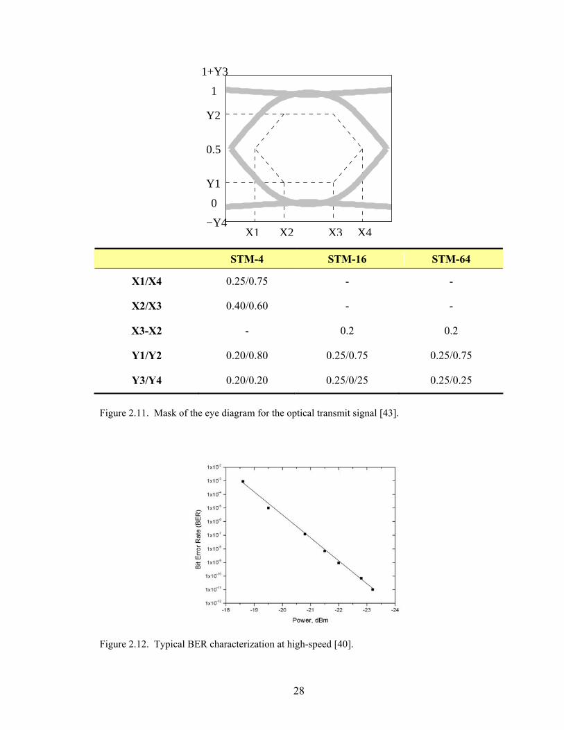
The SONET/SDH standards provide parameters and values for optical interfaces.
For the transmitter parts of such interfaces, they recommend an eye pattern mask to
specify general transmitter pulse shape characteristics, including rise time, fall time, pulse
overshoot, pulse undershoot, and ringing. The parameters in specifying the mask of the
transmitter eye diagram are shown in Figure 2.11.
2.5.3 Bit error rate (BER) measurements
The definition of BER is simply the ratio of the erroneous bits to the total number
of bits transmitted, received, or processed over some stipulated period, usually expressed
as ten to a negative power. For example, a ratio of 10-10 means that one wrong bit is
received for every 10 billion bits transmitted. Thus, the BER is a parameter of describing
the quality of signals in digital systems. In addition, the specification for BER is
dependent on the application requirements.
The power from the transmitter is large enough that if it were to arrive un-
attenuated at the system receiver, error-free communication would occur. System
performance in terms of BER is often characterized in terms of the amount of attenuation
between the transmitter and receiver. Similarly, the BER can be characterized in terms of
power level at the receiver. Figure 2.12 shows [40] a typical BER characterization of a
high-speed system. As the received power is decreased, the signal-to-noise ratio is
reduced and the probability of a bit being received in error increases.
28
−Y4
1
0.5
Y2
Y1
X2 X3 X4
0
1+Y3
X1
STM-4 STM-16 STM-64
X1/X4 0.25/0.75 - -
X2/X3 0.40/0.60 - -
X3-X2 - 0.2 0.2
Y1/Y2 0.20/0.80 0.25/0.75 0.25/0.75
Y3/Y4 0.20/0.20 0.25/0/25 0.25/0.25
Figure 2.11. Mask of the eye diagram for the optical transmit signal [43].
Figure 2.12. Typical BER characterization at high-speed [40].
29
CHAPTER III
DESIGN OF LOW-POWER CMOS LASER DRIVER
This chapter starts with the motivation for the design of high-speed and low-
power CMOS laser drivers. In addition to the design considerations of the laser driver,
preliminary simulations to verify the circuit schematic topology follow. Based on these
simulation results, the circuit is laid out with careful consideration for parasitic effects.
Then, with the data extracted from the layout, the driver circuit goes through a series of
simulations again with packaging effects, decoupling, and protection circuits for
electrostatic discharge (ESD).
3.1 Introduction
The motivation for the design and implementation of the high-speed and low-
power CMOS laser drivers arises from their critical role in the performance of optical
systems. To date, because of the rapid advances in multimedia applications, modern
communication systems have required the data links with ever-increasing capacity. This
necessitates high-speed optical communication systems. In such optical systems, the
design of a high-speed laser driver and receiver circuit is critical to the optimization of
the optical system because the electro-optic interface limits the maximum speed of the
overall systems as mentioned in Chapter II. In addition to the high-speed operation, the
laser driver should meet the systems requirements such as low BER and low electrical
power consumption.
30
Various solutions to the problems of designing of the high-speed laser driver
circuits have been demonstrated in GaAs [5] and InP [10, 12] based technologies to gain
the required performance, but the low-level of integration with other digital ICs limits the
sustainability of the end product for short-reach applications. Therefore, much effort to
implement the laser drivers in silicon CMOS technology has been made in both research
and commercial fields because of the high degree of integration of CMOS technology
with other components. Besides the advantages of high levels of integration, CMOS
technology has unique advantages of vast standard cell libraries, power efficiency, and
high yield compared with other IC technologies. Thus, in this research, the laser driver
was designed and fabricated in Twain Semiconductor Manufacturing Company’s
(TSMC) 0.18 µm mixed-signal CMOS technology through the MOSIS foundry service.
Table 3-1 summarized the specifications used in this research. The design goals
were established so as to meet the needs of two groups, researchers at a corporate
research partner and the integrated optoelectronics group at Georgia Institute of
Technology The laser driver was designed to have up to 10mA modulation currents and
10mA bias currents at 10 Gbps and also to have the lowest possible power consumption.

31
Table 3-1. Predetermined design goals of the laser driver.
Specifications Goal
Speed Greater than 10Gbps
Current Laser bias current: >10mA Modulation current : >10mA
Current Density < 1mA/µm2
Power Consumption As low as possible
3.2 Design Considerations
The aggressive demand for more bandwidth in communication systems has led to
increases in the density of integration and the switching speed of transistors. As
switching speed increases, high current switching within a short time period can generate
considerable dI/dt, and inductance (L) can lead to sizable voltage fluctuations, V=L·dI/dt.
This inductance results from the off-chip bonding wires and the on-chip parasitic
inductance of the power supply rails. This noise, called simultaneous switching noise,
delta I noise, or I∆ noise [44, 45], can seriously degrade signal integrity and is one of the
main noises that affects the design of laser drivers. Therefore, in this research the
creation of a high-speed operating laser driver relies on the differential topology because
it is immune to delta I noise [46].
Differential drivers offer many advantages over single-ended circuits. First, they
can maintain a relatively constant supply current by canceling unwanted common-mode
signals, thus minimizing delta I noise. Second, if the signals remain truly symmetry, they
can reduce cross talk. Third, their complementary signals with symmetric transients

32
simplify the design of wideband signal transmission interconnects, resulting in improved
eye diagrams at higher data rates [47]. Finally, they have low common-mode gain, a
feature can help prevent oscillation despite the presence of unwanted common-mode
feedback resulting from packaging parasitics.
The laser driver is designed to modulate a laser with a serial data stream and
provides dc bias current to the laser. The circuit schematic for the laser driver is depicted
in Figure 3.1.
VSS
VDDVDD
M1
M3 M4
I2
M2
M5 M6 M7
Z1Laser
Ibias
Imod
VSS
In1
In2
Current Swith (CS)
I1
Figure 3.1. Schematic of laser driver.
It consists of a differential current switch (CS) and current mirrors (I1, I2). The
current switch consists of two matched enhanced MOS transistors, M1 and M2. As the
size of the input transistors increases, higher output current are achievable. However,
33
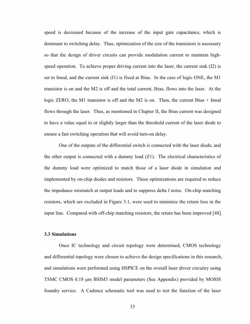
speed is decreased because of the increase of the input gate capacitance, which is
dominant to switching delay. Thus, optimization of the size of the transistors is necessary
so that the design of driver circuits can provide modulation current to maintain high-
speed operation. To achieve proper driving current into the laser, the current sink (I2) is
set to Imod, and the current sink (I1) is fixed at Ibias. In the case of logic ONE, the M1
transistor is on and the M2 is off and the total current, Ibias, flows into the laser. At the
logic ZERO, the M1 transistor is off and the M2 is on. Then, the current Ibias + Imod
flows through the laser. Thus, as mentioned in Chapter II, the Ibias current was designed
to have a value equal to or slightly larger than the threshold current of the laser diode to
ensure a fast switching operation that will avoid turn-on delay.
One of the outputs of the differential switch is connected with the laser diode, and
the other output is connected with a dummy load (Z1). The electrical characteristics of
the dummy load were optimized to match those of a laser diode in simulation and
implemented by on-chip diodes and resistors. These optimizations are required to reduce
the impedance mismatch at output loads and to suppress delta I noise. On-chip matching
resistors, which are excluded in Figure 3.1, were used to minimize the return loss in the
input line. Compared with off-chip matching resistors, the return has been improved [48].
3.3 Simulations
Once IC technology and circuit topology were determined, CMOS technology
and differential topology were chosen to achieve the design specifications in this research,
and simulations were performed using HSPICE on the overall laser driver circuitry using
TSMC CMOS 0.18 µm BSIM3 model parameters (See Appendix) provided by MOSIS
foundry service. A Cadence schematic tool was used to test the function of the laser

34
driver and estimate its speed. If the simulation results meet the design specifications, the
layout of circuit were performed, then the circuitry was re-simulated using the extracted
SPICE file from a Cadence layout tool to obtain information of parasitic parameters,
which can be generated and calculated from the layout, are not generally considered in
schematic simulation but play a significant role in high-speed circuit performance. The
flowchart of the simulation process is depicted in Figure 3.2.
Figure 3.2. The flowchart of the simulation processes.

35
3.3.1 Schematic-based simulations
Figure 3.3 shows the transient response of the driver at 10 Gbps in schematic
simulations. The top trace represents the pseudo random bit sequence (PRBS) input
signal at 10 Gbps, and the middle trace is the output currents of laser diode. The bottom
plot shows the eye diagram used to examine the intersymbol interference (ISI) effects
that result from the limited circuit bandwidth or from any imperfection that affects the
magnitude or phase response of a system [26]. As shown in the simulation results, when
only on-chip parasitics are considered, the laser driver is working properly with 10mA
modulation current at laser diode and variable laser bias currents at design specifications.
However, this simulation shows results only for the functional verification of the laser
driver. Therefore, off-chip parasitic and packaging effects should be included in the
overall circuit simulations.

36
Voltages (lin)
1.35
1.4
1.45
1.5
1.55
1.6
1.65
Time (lin) (TIME)
0 2n 4n 6n 8n 10n
DIFFERENTIAL PRBS 10 GBPS INPUT
Current 1 (lin)
6m
8m
10m
12m
14m
16m
18m
Time (lin) (TIME)
0 2n 4n 6n 8n 10n
LASER CURRENT
Current 1 (lin)
6m
8m
10m
12m
14m
16m
18m
Voltages (lin) (eye)
0 500m 1
EYE DIAGRAM
Figure 3.3. Simulated transient response of laser driver design at 10 Gbps with on-chip parasitics only.
After securing the preliminary simulation results, the voltage reference circuit is
used to provide a stable dc voltage at the input node regardless of the variation of the
power supply ripple. This circuit is based on the idea of using a negative feedback
amplifier to keep the voltage across R, as shown in Figure 3.4(a). The implementation of
this voltage reference circuit is illustrated in Figure 3.4(b). The operating principle of the
circuit is briefly described as follows. If the current IR and I1 are assumed as a constant
value, the reference voltage (Vref) is given by
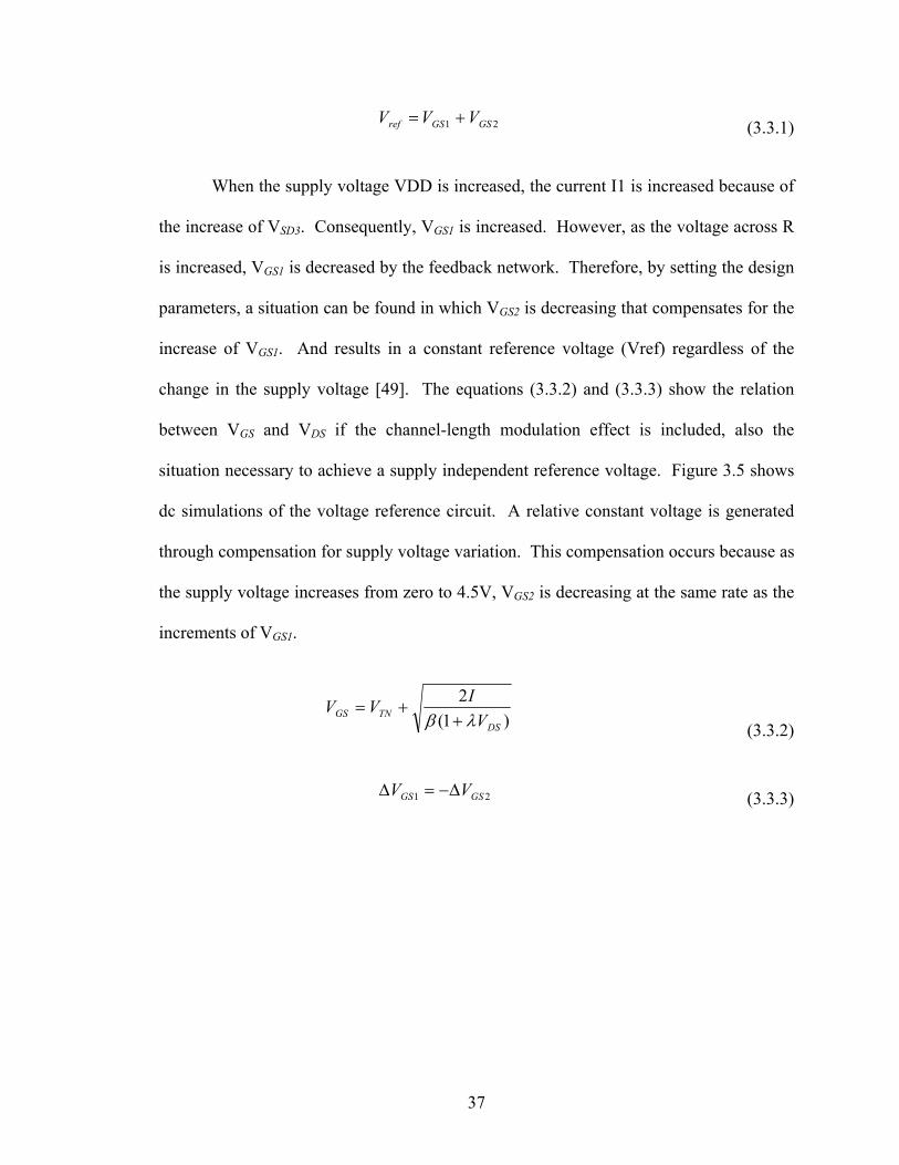
37
21 GSGSref VVV += (3.3.1)
When the supply voltage VDD is increased, the current I1 is increased because of
the increase of VSD3. Consequently, VGS1 is increased. However, as the voltage across R
is increased, VGS1 is decreased by the feedback network. Therefore, by setting the design
parameters, a situation can be found in which VGS2 is decreasing that compensates for the
increase of VGS1. And results in a constant reference voltage (Vref) regardless of the
change in the supply voltage [49]. The equations (3.3.2) and (3.3.3) show the relation
between VGS and VDS if the channel-length modulation effect is included, also the
situation necessary to achieve a supply independent reference voltage. Figure 3.5 shows
dc simulations of the voltage reference circuit. A relative constant voltage is generated
through compensation for supply voltage variation. This compensation occurs because as
the supply voltage increases from zero to 4.5V, VGS2 is decreasing at the same rate as the
increments of VGS1.
)1(2
DSTNGS V
IVVλβ +
+= (3.3.2)
21 GSGS VV ∆−=∆ (3.3.3)

38
(a) (b)
Figure 3.4. (a) A simplified supply-independent voltage reference circuit. (b) The implementation of a voltage reference circuit.
(a) (b) Figure 3.5. Simulation results of the voltage reference circuit. (a) represents the Vref and (b) represents the change of the Vgs1 and Vgs2. As the value of Vgs1 is increased, the Vgs2 is decreased, resulting in a compensated reference voltage.
One of the critical steps to design the laser drivers is arriving at an electrical
equivalent circuit that is the equivalent of a laser diode so that the transient behavior
common to laser diode can be accurately modeled. Most of researchers who have
39
reported on the design of laser drivers have focused mainly on the design. They have
paid no heed to the electrical characteristics of laser diodes, assuming instead that the
laser as a passive resistor [50-55]. However, considering the laser diode as a passive
resistor require more conditions to drive laser diodes externally. For example, if a laser
diode is assumed to be 50 ohm resistor and the value of the modulation currents of the
resistor is 10 mA, then a voltage drop across the resistor is only 0.5 V. However, most of
laser diodes require about 1.2 V for a standard edge-emitting laser and 1.5 V for VCSEL
as a turn-on voltage. Therefore, the laser drivers need an external bias tee to provide the
turn-on voltage. The utilization of external and expensive high-speed bias tee cannot be
included in CMOS solutions. In addition, laser driver circuitry based on a more precise
laser model can solve the difficulties in interfacing circuitry with a laser diode. Generally,
laser drivers require complicated matching networks to compensate for overshoot and
ringing. The more precise model a circuit designer has, the less effort required for
matching networks. Therefore, more optimized systems can be obtained.
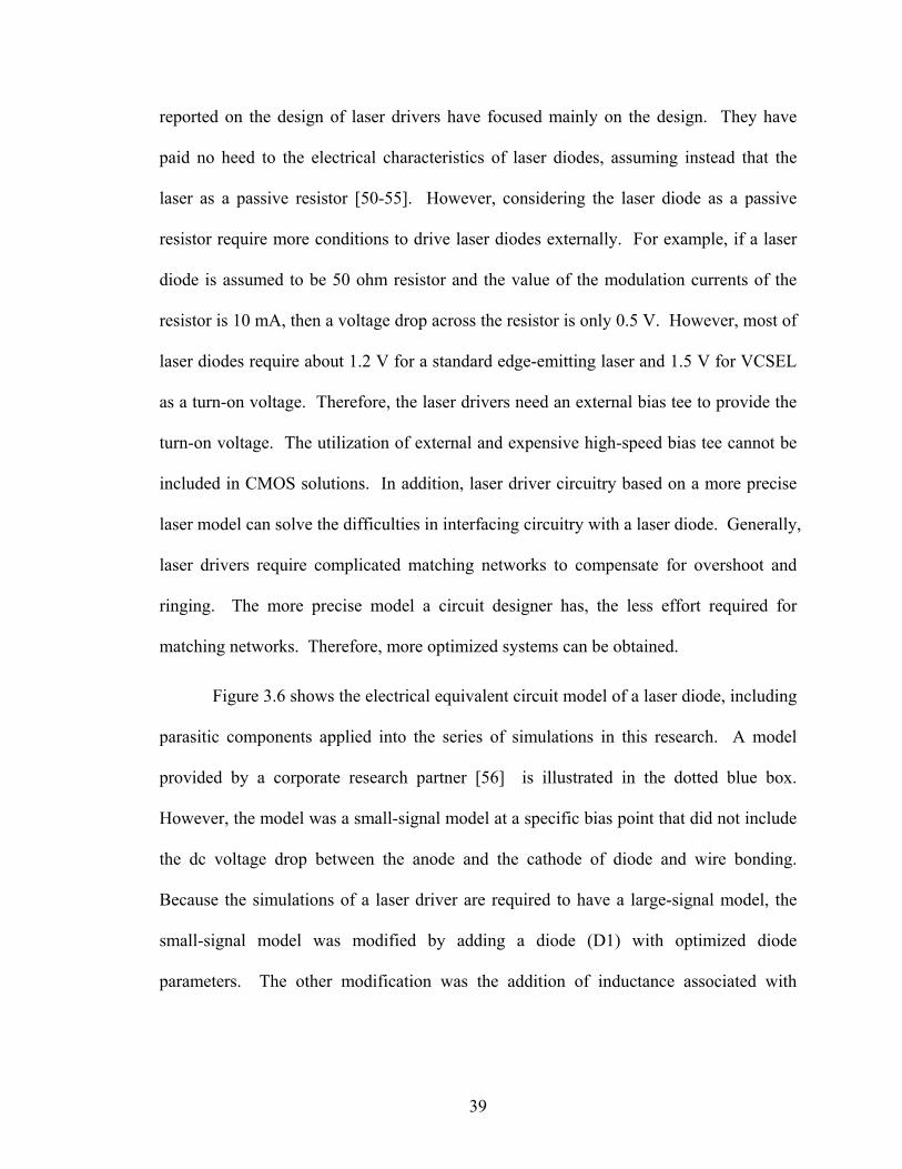
Figure 3.6 shows the electrical equivalent circuit model of a laser diode, including
parasitic components applied into the series of simulations in this research. A model
provided by a corporate research partner [56] is illustrated in the dotted blue box.
However, the model was a small-signal model at a specific bias point that did not include
the dc voltage drop between the anode and the cathode of diode and wire bonding.
Because the simulations of a laser driver are required to have a large-signal model, the
small-signal model was modified by adding a diode (D1) with optimized diode
parameters. The other modification was the addition of inductance associated with
40
bonding wires so that in simulations the model would match the dc characteristics of the
measured data of laser diodes.
The right side of Figure 3.6 shows the results of the optimization of the diode
parameters to build the large-signal model of the laser diode. The black line represents
the measured dc data of the laser diode, and the red line represents the dc characteristics
of the simulated diode with the optimized diode parameters. As shown in the curve-
fitting plot, the optimized diode parameters are matched into the measured data. Now,
the modified large-signal model can be applied to the simulations. By using this model,
the optical output of the laser is considered an electrical output that can be displayed by
SPICE.
Anode Bonding Wire
Bonding Wire
Cathode
C2
C1R1
R2
L1 Laser Model
D1
Figure 3.6. The equivalent circuit of a laser diode and parameter fitting for bias information.
After the schematic simulation results meet the desired specifications, the next
step is to perform a series of simulations based on the layout. The considerations in the

41
layout of circuitry will be presented in the next section, and the layout-based simulation
results will be discussed.
3.3.2 Layout-based simulations
As operating speed increases, design of high-speed CMOS circuits requires
consideration of the effects of layout and packaging parasitics. This is important because
the results of the results of schematic simulations are inaccurate because of missing
parasitic components such as capacitances, resistances, diodes, and inductance, all of
which often play an important role in circuit performance as operating speed increases
[57, 58].
To emphasize the importance of the layout-base simulations, an example is shown
in Figure 3.7 that compares the schematic-based simulations and the layout-based
simulations. Parasitic effects including power supply inductance were added into the
layout-based simulations. The first trace showed the eye diagram in schematic-based
simulations. The second trace represents the eye diagram results of layout-based
simulations. In comparing the results, the layout-based simulation showed more rise and
fall time and signal degradations such as jitters and eye closure than the results obtained
from the schematic-based simulations. Therefore, a layout-based simulation is vital to
anticipating the real transient behaviors at high-speed applications and is one of critical
stage in the implementing high-speed circuitry. In addition, the last eye diagram
represents the transient response of the laser driver with a 50 ohm resistor. As shown in
the eye diagram, the output current flowing resistors were not affected by parasitics or

42
packaging effects; therefore, simulations with a more accurate equivalent model are a
much better approach to implementing laser drivers.
Figure 3.7. Comparisons of layout-based simulation vs. schematic simulations. The top trace represents the schematic simulation. The second trace represents the layout-based simulations. The last trace indicates the 50 ohm load laser driver instead of a laser model.
Since the layout could generate big differences in schematic simulations as shown
in previous simulations, the laser driver was laid out carefully to minimize unwanted

43
behaviors such as common-mode noise, signal delay, and crosstalk. The transistor size
has been optimized for high-speed and relatively large current operation, and a multiple
finger structure has been used to reduce the input capacitances, which are the dominant
factor of switching delay. Matching the performance of two input transistors is very
important to overall laser driver operation. Thus, input transistors M1 and M2 have
identical shapes with respect to signal path. Both M1 and M2 transistors of a differential
pair in a laser driver consist of M1A and M1A, and M2A and M2B, respectively. At the
upper left corner, a matching diode also included in the layout. An M4 transistor shown
in Figure 3.1 is divided into two M3A and M3B, which are identical to create a
symmetrical layout. Although the surroundings seen by M1 and M2 are different because
of the presence of current mirrors to provide bias and modulation current and matching
diodes, matching performance can be normally improved by making the intermediate
surroundings identical. This general rule has been applied repeatedly to all components.
The symmetric structure of the input transistors along the signal path is shown in Figure
3.8.
The metal lines and vias have the current density rule in the process. Therefore,
the width of metal lines and the number of vias should be carefully optimized. For
example, the width of the power supply rail should be more than 20 µm for the current
driving capacity of 20 mA. If 10 mA currents flow through a five µm-wide transistor, the
transistor should have a multiple finger structure to keep the current density rule.
However, making every metal line wide unnecessarily wastes space because as line width
increases, the parasitic capacitance and resistance also are increased, which can
significantly degrade performance or generate unwanted noise. Therefore, it is necessary

44
that the layout designer should track all currents at every node to meet the current density
rule, and the metal width and number of vias should be optimized for reliable operations
in high-speed circuitry. To minimize the degradation of the input and output signal
resulting from the packaging effects at 10 Gbps or higher speed, Cascade 100 µm pitch-
to-pitch ground-signal-ground-signal-ground (GSGSG) probes are used at the input and
output. These probes are supposed to operate up to 40 GHz.
Figure 3.8. Differential switch divided into two parts to make a symmetrical layout along the signal path.
Electrostatic discharge (ESD) protection circuits are connected to all pads. A
block diagram of the ESD protection circuit is illustrated in Figure 3.9. The current flow

45
is always in the diode’s forward direction and positive ESD pulses are clamped to
ESD_VDD, and negative ESD pulses are clamped to ESD_VSS. A screen capture of the
laser driver layout is shown in Figure 3.10. In addition, a screen capture of the whole
chip image is shown in Figure 3.11. Three types of laser drivers are located in the middle
of the chip, and a red rectangle in the middle represents the integration site for thin film
devices. ESD circuits surround the whole chip and the transimpedance amplifier is
located in the left half of the chip. The right side of Figure 3.11 shows the test structures
for characterization of transistors.
ESD_VSS
ESD_VDD
ESD_VDD
ESD_VDD
Laser Driver
ESD_VSS
ESD_VSS
ESD_VSS
Modulation
Bias
VSS
VDD
ESD_VDD
Figure 3.9. Block diagram of ESD circuitry.

46
Figure 3.10. The layout of designed laser driver circuits with ESD circuitry, GSGSG probes, MiM capacitors
Figure 3.11. The layout out of whole chip, which includes laser driver, transimpedance amplifier. The empty space in the middle of chip is for a laser and detector integration site.
47
The structure consisted of two sizes of transistors with 10 µm and 20 µm of
channel width. In addition, they can be measured by microwave on-wafer probes. Since
there are process variations, these structures could be one of the sources to verify the
deviations from expected performances of the model used in simulations. Therefore, it is
very helpful to find the optimized conditions for circuit operations when the circuit is
tested. The integration site in the middle of chip is just empty space when thin film
devices are integrated onto the CMOS chip.
Moreover, the TSMC 0.18 µm mixed-signal CMOS process has a minimum
density rule, which means each metal and poly layer density is much greater than or equal
to a certain percentage that is derived from total chip area. For example, a minimum poly
layer should be over 14 % of the chip area. The density of a layer in a particular region is
calculated as total area covered by drawn features on that layer divided by total the chip
area. The minimum density rule came from a process using chemical-mechanical
polishing (CMP) to achieve planarity for a fine-featured process. Therefore, to meet the
minimum density rule, the right side of the chip shown in Figure 3.11 was filled with
dummy metal and with poly layers shown as a blue rectangle. The next step for the
layout-based simulations is to extract a SPICE file from the drawn layout using the
Cadence layout tools. The extracted SPICE file, including the parasitic components, is
attached to the Appendix. In addition to the parasitic components, the packaging
parasitics should be included in the simulations. In Figure 3.12, the block diagram of the
packaging parasitic simulation is illustrated to determine the value of decoupling
capacitors to suppress the delta I noise, which cannot be completely removed by
differential topology alone.

48
Figure 3.12. Simplified circuit schematic: The circuit model includes parasitic inductance, Lcable on cable, Ltrace of the power line on the PCB, and Lbonding on wire bonding.
Figure 3.13 shows the transient response with packaging components in which the
parasitic inductance was assumed to be 10nH for the power supply interconnect (Lcable),
5nH for traces on the test board (Ltrace), and 2nH for the bonding wires (Lbonding). The
top trace represents the output current of the laser driver, the second trace is the eye
diagram of the laser current, and the last trace represents the voltage fluctuation in power
supply rails. The eye diagram in Figure 3.13 shows that circuit performance is degraded
significantly because of these packaging and parasitic components. The current
fluctuations in power supply rails have about 10 mAp-p. To solve the problem of
degradation of signal integrity, a decoupling technique was used in this research.
Decoupling capacitance is the major consideration in controlling impedance and
noise on power supply. The effectiveness of the decoupling capacitors can be proven by
a simple equation.
CI
dtdV
dtdVCI =⇒= (3.3.4)

49
As the value of the decoupling capacitance C is increased, the voltage fluctuation
dV/dt is decreased. Therefore, the decoupling capacitor between the power supply rails
can reduce the power supply ripple. Capacitors used for decoupling purposes are only
capacitive at low frequencies. At high frequencies, the capacitor becomes an inductor
whose inductance is related to the path that current takes through the capacitor, almost as
if it were made of a conductive material. Resonance occurs at frequency
LCf
π21
= (3.3.5)
where L and C are the value of capacitance and inductance respectively. The
impedance of the capacitor at resonance is the equivalent series resistance (ESR). A
decoupling capacitor is modeled as a resistor, capacitor, and inductor in series, as shown
in Figure 3.14. Therefore, the value of the capacitors should be carefully chosen because
capacitors also have their own parasitic inductance and resistance.

50
Figure 3.13. Transient simulation with line parasitics and no decoupling capwnsgmlacitors. The top trace represents the output current of laser diode, the second trace shows the eye diagram of the laser driver, and the last trace represents the voltage fluctuation of the power supply rails.
Figure 3.14. Equivalent circuit model of capacitor.
To determine the value of the decoupling capacitor, it is necessary to estimate the
instantaneous current required when all the outputs of an IC switch from LOW to HIGH.

51
The amount of capacitance required to maintain the power supply to within some ripple
specification is calculated by
nVddfI
dVdQC
c ××==
2 (3.3.6)
where dQ is the charge per burst, fc is the clock frequency, Vdd is the power
supply voltage, and n is the fraction of ripple voltage allowed.
In this research, an on-chip metal-insulator-metal (MiM) based on the equivalent
model provided by the MOSIS foundry, shown in Figure 3.15 (a), was used as the
decoupling capacitor. Here, Rs, Ls, and Cmin represent the general capacitor model
shown in Figure 3.14. Moreover, Coxm, Rsub, and Csub were added to represent the
substrate effects of the chip. Figure 3.15 (b) shows the s-parameter simulation with this
capacitor model. The bottom plot shows 14 GHz of resonance frequency of this
capacitor, which is effective as a capacitor below 14 GHz. The top plot represents the
broad coupling at high frequency range.
Figure 3.16 and Figure 3.17 show the frequency response of the laser driver with
and without decoupling capacitors, respectively. By using 90 parallel MiM capacitors for
a total capacitance of around 85.59 nF, a decoupling technique was employed with the
laser driver. As shown in Figure 3.16, the packaging components created huge peaks of
output currents at a relatively low frequency range, and Figure 3.17 shows the decoupling
technique effectively suppressed the peaking. In addition, the frequency response shows
the broadband operations of the laser over 10 Gbps.

52
Figure 3.15. (a) Equivalent circuit of MiM capacitor. (b) the MiM capacitor simulated s-parameters, S21 (top) shows broad coupling and S11 (bottom) shows the resonance frequency of the capacitor.
Figure 3.16. Frequency response of the laser driver without decoupling capacitors.

53
Figure 3.17. Frequency response of the laser driver with decoupling capacitors.
The transient response at 10 Gbps with decoupling capacitors is shown in Figure
3.18. The first trace represents the input voltage of the laser driver, the second one shows
the eye diagram of the output currents, and the third one shows the voltage fluctuation in
power supply rails. By the decoupling capacitors, compared to the eye diagram in Figure
3.13, the eye diagram shown in Figure 3.18 has larger open eyes, which means the laser
driver can operate at 10 Gbps. In addition, decoupling capacitors suppressed by about
70 % the power supply ripple shown in the last trace.
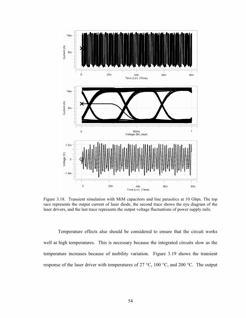
54
Figure 3.18. Transient simulation with MiM capacitors and line parasitics at 10 Gbps. The top race represents the output current of laser diode, the second trace shows the eye diagram of the laser drivers, and the last trace represents the output voltage fluctuations of power supply rails.
Temperature effects also should be considered to ensure that the circuit works
well at high temperatures. This is necessary because the integrated circuits slow as the
temperature increases because of mobility variation. Figure 3.19 shows the transient
response of the laser driver with temperatures of 27 °C, 100 °C, and 200 °C. The output

55
becomes little bit slower as the temperature increases but still works within the design
specifications, as indicated by the open eye diagram at 200 °C.
Figure 3.19. The eye diagram of laser driver at 10 Gbps with the temperature variations. The yellow line is at 27 °C, the red line is at 100 °C, and the cyan line is at 200 °C.
3.4 Experimental Results
3.4.1 Test setup
The laser driver circuits were fabricated using a TSMC 0.18 µm mixed signal/RF
process using non-epitaxial wafers. This CMOS process has a silicide block, thick gate
oxide (3.3V), NT_N, deep n well, Thick Top Metal (inductor), and MiM options [59].
Figure 3.20 illustrates the block diagram of measurement setup for testing the
laser driver. An HP 71512B Bit Error Rate Tester (BERT) generates different modes of
pseudo random bit streams (PRBS) and measures the probability of a transmitted data
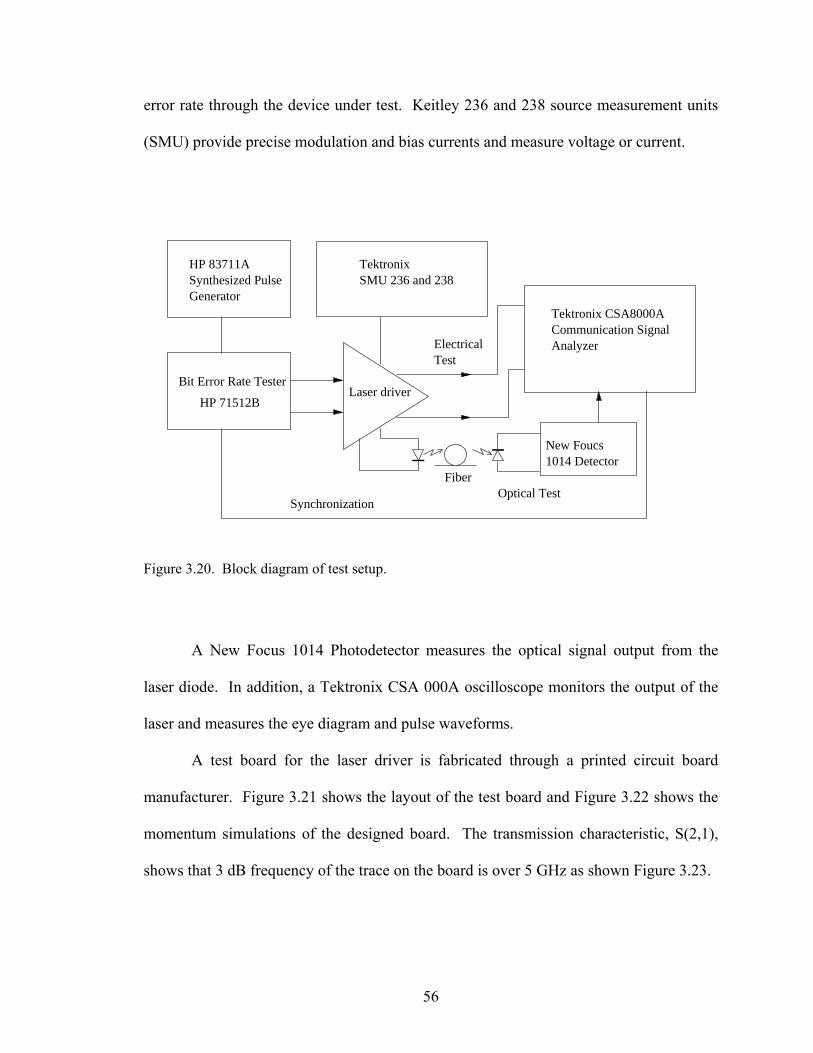
56
error rate through the device under test. Keitley 236 and 238 source measurement units
(SMU) provide precise modulation and bias currents and measure voltage or current.
Fiber
HP 83711ASynthesized Pulse Generator
Bit Error Rate Tester
HP 71512B
TektronixSMU 236 and 238
Laser driver
Optical TestSynchronization
Tektronix CSA8000ACommunication SignalAnalyzerElectrical
Test
New Foucs1014 Detector
Figure 3.20. Block diagram of test setup.
A New Focus 1014 Photodetector measures the optical signal output from the
laser diode. In addition, a Tektronix CSA 000A oscilloscope monitors the output of the
laser and measures the eye diagram and pulse waveforms.
A test board for the laser driver is fabricated through a printed circuit board
manufacturer. Figure 3.21 shows the layout of the test board and Figure 3.22 shows the
momentum simulations of the designed board. The transmission characteristic, S(2,1),
shows that 3 dB frequency of the trace on the board is over 5 GHz as shown Figure 3.23.

57
Figure 3.21. Layout of test board of the laser driver.
Figure 3.24 is a picture of the fabricated FR4 PCB test board. This test board is
only used to provide the power supplies, dc bias, modulation current, and ESD power
supplies to avoid signal degradation at high frequency. The input and output will be
performed by probing with GSGSG probes. The box on the backside of the test board
indicates the external decoupling chip capacitor site in case internal on-chip capacitors
are not enough to suppress the supply noise. The chip is mounted in the center of the
PCB test board, and then all pads are wire-bonded to the board. Figure 3.25 shows a
microphotograph of the laser driver with wire bonding.

58
Figure 3.22. Momentum simulations of the FR4 test board with HPADS.
Figure 3.23. Transmission characteristics of the traces on the test board.

59
Figure 3.24. Picture of test board.
Figure 3.25. A microphotograph of the wire-bonded laser driver.

60
3.4.2 Measurements
An eye diagram and a pulsed waveform of the laser driver were measured using
211-1 non-return to zero (NRZ) PRBS input, which simulates the real data pattern
specified in SONET specifications. The target operating speed is more than 10 Gbps.
Bias currents and laser dc currents were adjusted to achieve optimized operating.
Tektronix communication analyzer (CSA 8000A) was used as an electrical output and
captured the eye diagrams for the operating laser driver.
Figure 3.26 and Figure 3.27 represent the measured eye diagram at 1 and 5 Gbps
to verify the broadband operation of the laser driver. Figure 3.28 and 3.29 show the
measured pulsed waveforms and the eye diagram at the electrical output of the laser
driver, respectively. The input signal is a 211-1 pseudorandom bit sequence (PRBS) at 10
Gbps with 800 mVp-p amplitude. The amplitude of the signal output is 350 mVp-p into a
50 ohm load with bit error rate greater than (BER) of 3.11×10⁻¹⁴. The overall power
consumption is 65.5 mW. The SONET OC-192/STM-64 transmitter mask was provided
for comparison in Figure 3.30. It shows that the output is good enough to meet the eye
pattern specifications of SONET OC-192/STM-64 recommendations. Figure 3.31 shows
the measured eye diagram at 12 Gbps. It showed the laser driver could be operating at 12
Gbps. The details of optimized bias information and specifications at 10 Gbps are
summarized in Table 3-2.

61
Table 3-2. Optimized bias conditions and specifications of the laser driver.
Specifications Conditions
VDD 2.5 V
VSS 0 V
Laser modulation up to 12 mA
Power Dissipation 65.5W
Speed over 10 Gbps
BER > 3.11×10⁻¹⁴
Area 825 um × 613 µm
Figure 3.26. Measured eye diagram at 1 Gbps.
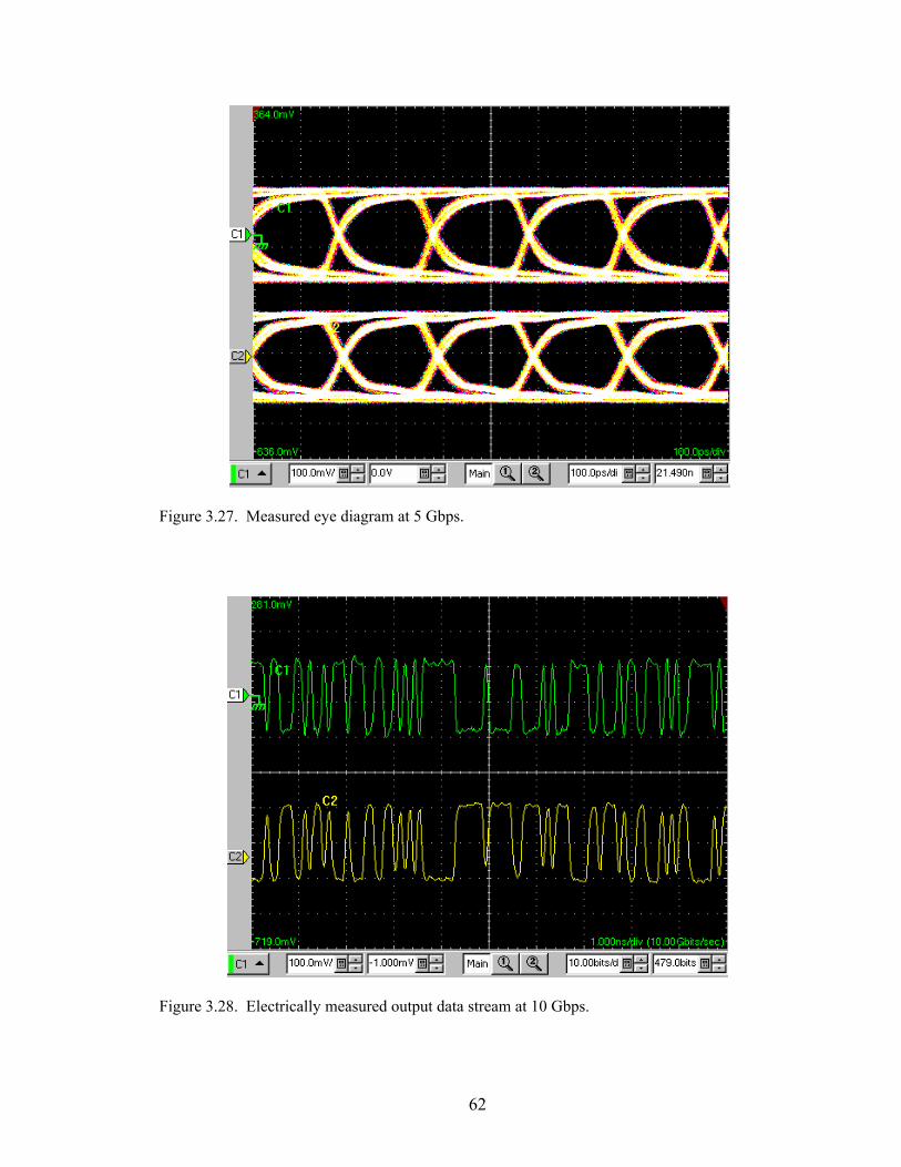
62
Figure 3.27. Measured eye diagram at 5 Gbps.
Figure 3.28. Electrically measured output data stream at 10 Gbps.
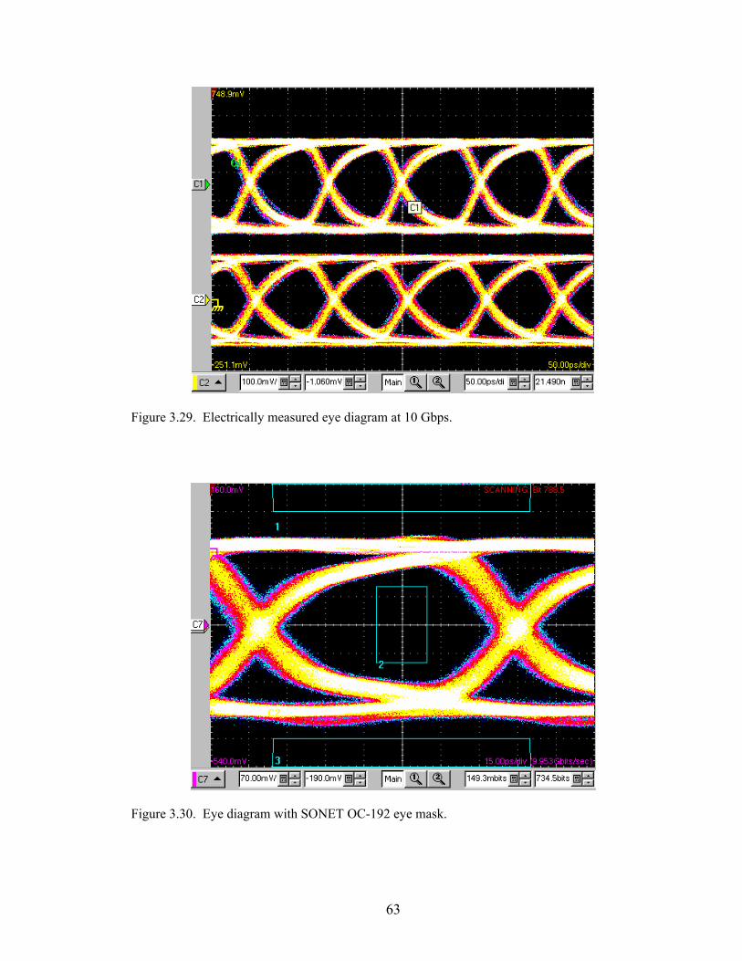
63
Figure 3.29. Electrically measured eye diagram at 10 Gbps.
Figure 3.30. Eye diagram with SONET OC-192 eye mask.
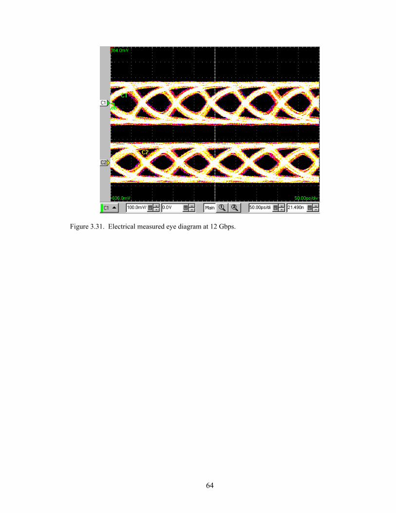
64
Figure 3.31. Electrical measured eye diagram at 12 Gbps.

65
CHAPTER IV
THIN FILM LASER INTEGRATION ONTO CMOS
CIRCUITS
A high-speed optical transmitter consists of a laser driver circuit and a laser diode
as mentioned in Chapter II. This chapter discusses thin film integration in the
implementation of optical transmitters. The advantages of the approaches are followed
and compared with other solutions used to implement the optical transmitters. Then, thin
film laser devices fabricated at Georgia Tech are discussed.
4.1 Introduction
A smart pixel is defined as an optoelectronic structure composed of electronic
processing circuitry enhanced with optical inputs and/or outputs [60]. The basic concept
of a smart pixel is to integrate both electrical systems and individual optical device on a
common chip to take advantage of electrical circuit complexity and the speed of optical
devices [61]. Arrays of these smart pixels would bring with them the advantage of
parallelism that could provide new opportunities to utilize dramatically greater
bandwidths. A number of approaches have been studied to implement smart pixels. The
most common approaches in use today are monolithic integration and hybrid integration.
Monolithic integration is a technique that allows both electronics and optical
devices to be integrated in a common semiconductor material in a single growth process
or by utilizing a re-growth technique [61]. This approach, potentially, would produce

66
high-performance smart pixels. The speed and noise performance of optoelectronic
devices can be improved by monolithic integration because of the reduction of parasitic
components. A further advantage of monolithic integration on a compound
semiconductor comes from having much better heat-conduction than silicon technology,
an advantage can directly improve the power efficiency of individual components such as
lasers and transistors. In addition, the monolithic integration of many elements on a
single chip makes the number of components required for system construction much less
than when discrete devices are used. This would result in more compact and more
reliable system.
However, two major challenges remain before these advantages result in a
mainstream technology: simultaneous optimization of both the optical devices and the
electronic circuitry and a general lack of maturity of compound semiconductor
technology. The optimization techniques used for electronic circuitry to provide
increased functionality are not the same as the optimization techniques required to
produce high-quality optical devices. Therefore, trade-offs must be made that reduce
some performance metric associated with the overall system. If the re-growth technique
is used, the large difference in lattice constants between direct-gap III-V compounds and
silicon has prevented the monolithic integration of semiconductors with silicon-based
electronic circuitry. Moreover, it is necessary to develop new techniques or complex
processing to implement the monolithic optical system.
The second challenge, technological maturity, is associated with the differences in
the technological maturity of silicon processes compared with those of compound
semiconductors. Mainstream silicon-based technology such as CMOS has been
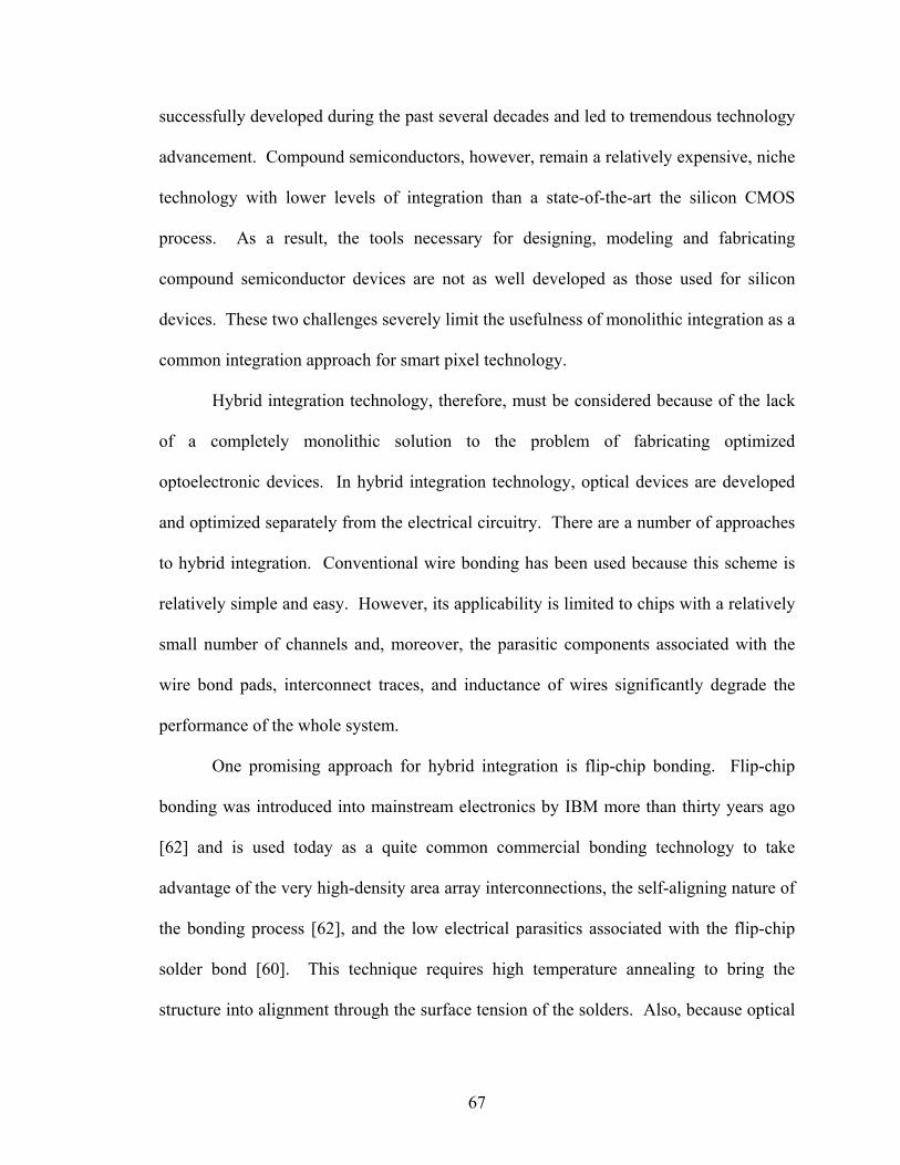
67
successfully developed during the past several decades and led to tremendous technology
advancement. Compound semiconductors, however, remain a relatively expensive, niche
technology with lower levels of integration than a state-of-the-art the silicon CMOS
process. As a result, the tools necessary for designing, modeling and fabricating
compound semiconductor devices are not as well developed as those used for silicon
devices. These two challenges severely limit the usefulness of monolithic integration as a
common integration approach for smart pixel technology.
Hybrid integration technology, therefore, must be considered because of the lack
of a completely monolithic solution to the problem of fabricating optimized
optoelectronic devices. In hybrid integration technology, optical devices are developed
and optimized separately from the electrical circuitry. There are a number of approaches
to hybrid integration. Conventional wire bonding has been used because this scheme is
relatively simple and easy. However, its applicability is limited to chips with a relatively
small number of channels and, moreover, the parasitic components associated with the
wire bond pads, interconnect traces, and inductance of wires significantly degrade the
performance of the whole system.
One promising approach for hybrid integration is flip-chip bonding. Flip-chip
bonding was introduced into mainstream electronics by IBM more than thirty years ago
[62] and is used today as a quite common commercial bonding technology to take
advantage of the very high-density area array interconnections, the self-aligning nature of
the bonding process [62], and the low electrical parasitics associated with the flip-chip
solder bond [60]. This technique requires high temperature annealing to bring the
structure into alignment through the surface tension of the solders. Also, because optical

68
devices are inverted during the flip-chip bonding process, when they are involved, the
substrate must be either transparent or removed during a subsequent process [60, 63, 64].
The other promising approach is thin film integration, also called epitaxial liftoff
(ELO). In this technology, optical devices are grown and optimized separately from
silicon circuitry and removed from the fabrication substrate using a technique called ELO,
and then bonded to the CMOS circuitry using either Van der Waals bonding or adhesion
between the host and ELO epitaxial layer. Some unique advantages of the thin film
integration technology are that because the thin film devices can be inverted from the
fabrication substrates, both sides of the thin film devices can be processed [63]. This is
an important feature when considering three-dimensional interconnect and structures [65]
and embedding OE devices into waveguides [63].
4.2 Thin Film Lasers
The material structure [66] of the thin film lasers developed by the integrated
optoelectronics group at Georgia Institute of Technology are illustrated in Table 4-1.
After the substrate of the laser was removed, the thin film lasers were then bonded to host
substrates, BCB coated silicon substrate, for verification of their functionality. L-I and
V-I measurements of the thin film lasers were performed. The measured threshold
currents were approximately 25 mA when the injected currents have a pulsed-mode input
with 10 % of duty cycle and 0.1 us pulse width. More details with different duty cycles
of injected currents are shown in Figure 4.1. As the duty cycle is increased, the thin film
laser has more optical power. However, going over 10 % of the duty cycle of the injected
currents decreased the optical power of the laser. The fabricated thin film laser, therefore,
showed an optimized operating point: 10 % of the duty cycle of the pulse current. In

69
addition, the measured V-I graph is shown in Figure 4.2. The thin film lasers have a
thermal problem that restricts the high power continuous-wave (CW) operation of the
laser, which is a normally used operating method for a laser driver. Therefore, the thin
film laser, in this research, should be operated with pulsed mode input currents to prevent
the thin film laser from harmful thermal damage.
Table 4-1. Thin film laser material structure.
Layers Thickness (µm)
InGaAs: p-contact 0.1
p-InP 1
InGaAsP (λ=1.3 µm) :
5 multiple quantum well
0.3
n-InP 1
n-InGaAs (n-contact) 0.2
n-InP 2
n-InGaAs (etch stop layer) 0.2
InP substrate

70
Figure 4.1. L-I measurement: the thin film laser on BCB coated silicon wafer. The measured threshold current is approximately 25 mA when the injected current has 10 % of the duty cycle.
Figure 4.2. V-I measurement: the thin film laser on BCB coated silicon wafer.
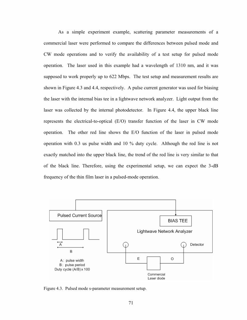
71
As a simple experiment example, scattering parameter measurements of a
commercial laser were performed to compare the differences between pulsed mode and
CW mode operations and to verify the availability of a test setup for pulsed mode
operation. The laser used in this example had a wavelength of 1310 nm, and it was
supposed to work properly up to 622 Mbps. The test setup and measurement results are
shown in Figure 4.3 and 4.4, respectively. A pulse current generator was used for biasing
the laser with the internal bias tee in a lightwave network analyzer. Light output from the
laser was collected by the internal photodetector. In Figure 4.4, the upper black line
represents the electrical-to-optical (E/O) transfer function of the laser in CW mode
operation. The other red line shows the E/O function of the laser in pulsed mode
operation with 0.3 us pulse width and 10 % duty cycle. Although the red line is not
exactly matched into the upper black line, the trend of the red line is very similar to that
of the black line. Therefore, using the experimental setup, we can expect the 3-dB
frequency of the thin film laser in a pulsed-mode operation.
Figure 4.3. Pulsed mode s-parameter measurement setup.
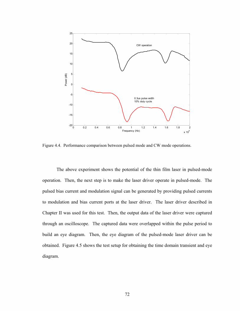
72
0 0.2 0.4 0.6 0.8 1 1.2 1.4 1.6 1.8 2
x 109
-20
-15
-10
-5
0
5
10
15
20
25
Frequency (Hz)
Pow
er (d
B)
CW operation
0.3us pulse width10% duty cycle
Figure 4.4. Performance comparison between pulsed mode and CW mode operations.
The above experiment shows the potential of the thin film laser in pulsed-mode
operation. Then, the next step is to make the laser driver operate in pulsed-mode. The
pulsed bias current and modulation signal can be generated by providing pulsed currents
to modulation and bias current ports at the laser driver. The laser driver described in
Chapter II was used for this test. Then, the output data of the laser driver were captured
through an oscilloscope. The captured data were overlapped within the pulse period to
build an eye diagram. Then, the eye diagram of the pulsed-mode laser driver can be
obtained. Figure 4.5 shows the test setup for obtaining the time domain transient and eye
diagram.
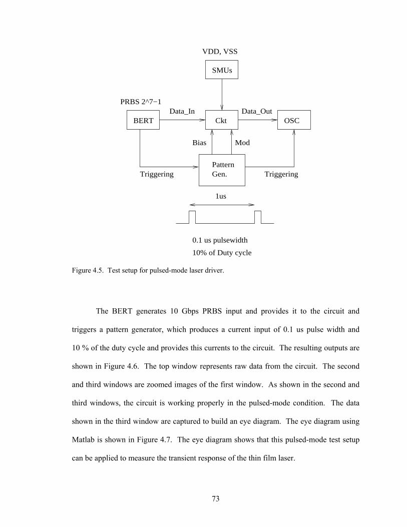
73
PRBS 2^7−1
Ckt
SMUs
BERT
PatternGen.
OSC
0.1 us pulsewidth
10% of Duty cycle
1us
Data_In Data_Out
VDD, VSS
Bias Mod
TriggeringTriggering
Figure 4.5. Test setup for pulsed-mode laser driver.
The BERT generates 10 Gbps PRBS input and provides it to the circuit and
triggers a pattern generator, which produces a current input of 0.1 us pulse width and
10 % of the duty cycle and provides this currents to the circuit. The resulting outputs are
shown in Figure 4.6. The top window represents raw data from the circuit. The second
and third windows are zoomed images of the first window. As shown in the second and
third windows, the circuit is working properly in the pulsed-mode condition. The data
shown in the third window are captured to build an eye diagram. The eye diagram using
Matlab is shown in Figure 4.7. The eye diagram shows that this pulsed-mode test setup
can be applied to measure the transient response of the thin film laser.

74
Figure 4.6. The output shows the pulsed-mode operation of the laser driver at the oscilloscope. Top window represents raw data captured at the output of the circuit. The second and third windows are zoomed data.
Figure 4.7. The eye diagram out of the pulsed data output.

75
4.3. Simulations
The electrical equivalent laser model used in Chapter III was modified to use the
thin film laser to simulate the optical transmitter. Initially, the small-signal impedance
out of the measured V-I characteristics was applied to the dominant factor of the model
from which the inductance of bonding wire was removed. It was removed because the
thin film laser will be connected with patterned metal line using conventional post-
processing techniques. Successful high frequency signal transmission through the
patterned metal line requires isolation from the lossy substrate. To insulate the lines from
the substrate, a 3 µm of layer of silicon dioxide (SiO2) is spun on the substrates.
Coplanar waveguide transmission lines are fabricated on silicon wafers with and without
SiO2 to compare the loss on the different substrates. Using the HPADS momentum
simulator, the characteristics of the transmission lines, 500 µm length, and 20 µm spacing,
on SiO2 coated silicon substrate were expected and compared to measured data, as shown
in Figure 4.8. The measured data results show that the loss characteristic of the
transmission line has little effects on the high frequency signaling when the 3 µm SiO2
coated silicon substrate is used. Compared with the transmission lines without the SiO2
on substrate, shown in Figure 4.9, which are expected to work properly below 1 GHz, the
transmission lines on SiO2 can be used at rates higher than 20 GHz without any
degradation of signal. The characteristics of transmission lines on a ceramic substrate, as
measured by a calibration kit used to measure high frequency devices working up to 40
GHz, show the almost identical characteristics as transmission lines on the SiO2 coated
silicon substrate. Therefore, the thin film laser model without the effects of the
inductance of bonding wires can be applied to the laser driver simulations. In addition,

76
the results of the momentum simulations show promise of delivering the characteristics
of various shapes of the transmission lines.
Figure 4.8. The comparison of the transfer characteristics (S21) of the transmission line between measurement and simulation.
Figure 4.9. The transfer characteristics of transmission lines on silicon substrate with and without SiO2 coatings.

77
The laser driver circuit used in Chapter III was used to perform transient
simulations with the modified thin film laser model. Figure 4.10 shows the results, and
the change of small-signal resistance does not critically affect the circuit’s operation at 10
Gbps with the open eye diagram. This simulation assumed that the inductance of
bonding wire was 0.1 nH and the small-signal resistance obtained from the V-I
measurement was 25 ohms.
Figure 4.10. Transient response of thin film laser.
4.4 Measurements
In previous sections, the thin film laser was bonded onto an oxide-coated silicon
substrate. The SiO2-coated silicon host substrate is very similar to a silicon CMOS

78
circuit. Using a transfer diaphragm heterogeneous integration process, a thin film laser
was integrated onto a silicon substrate that had 3 µm of SiO2 deposited onto it. All the
fabrication and integration processes were performed by Professor Nan Jokerst’s research
group at Georgia Tech. Figure 4.11 shows a microphotograph of the optical transmitter
with the thin film laser.
Figure 4.11. A microphotograph of the thin film laser integrated onto a CMOS circuit.
The transfer diaphragm heterogeneous integration process is illustrated in Figure
4.12. Once the thin film laser passes the functional test, the systems are bonded to the
test board used in Chapter III. The test board is designed, except differential inputs, with
all variable pads for adjusting biases. Differential inputs are provided by probing with
microwave probes. After bonding the system to the board, the laser driver is wire bonded
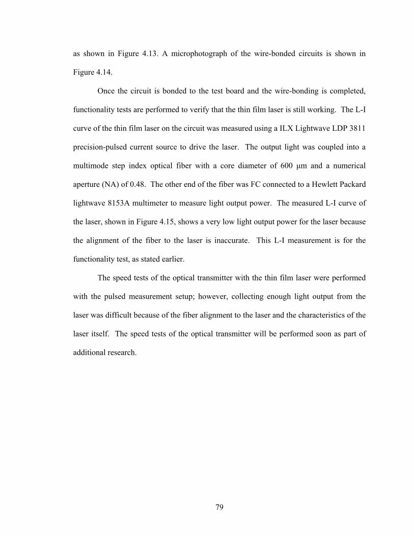
79
as shown in Figure 4.13. A microphotograph of the wire-bonded circuits is shown in
Figure 4.14.
Once the circuit is bonded to the test board and the wire-bonding is completed,
functionality tests are performed to verify that the thin film laser is still working. The L-I
curve of the thin film laser on the circuit was measured using a ILX Lightwave LDP 3811
precision-pulsed current source to drive the laser. The output light was coupled into a
multimode step index optical fiber with a core diameter of 600 µm and a numerical
aperture (NA) of 0.48. The other end of the fiber was FC connected to a Hewlett Packard
lightwave 8153A multimeter to measure light output power. The measured L-I curve of
the laser, shown in Figure 4.15, shows a very low light output power for the laser because
the alignment of the fiber to the laser is inaccurate. This L-I measurement is for the
functionality test, as stated earlier.
The speed tests of the optical transmitter with the thin film laser were performed
with the pulsed measurement setup; however, collecting enough light output from the
laser was difficult because of the fiber alignment to the laser and the characteristics of the
laser itself. The speed tests of the optical transmitter will be performed soon as part of
additional research.
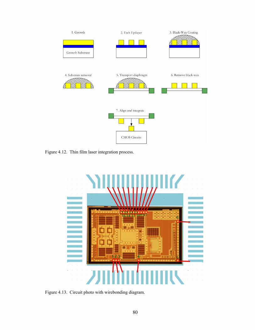
80
Figure 4.12. Thin film laser integration process.
Figure 4.13. Circuit photo with wirebonding diagram.

81
Figure 4.14. Integrated circuit photo with wirebonds.
0 5 10 15 20 25 30 35 40 45 50
0.0
0.2
0.4
0.6
0.8
1.0
Opt
ical P
ower
(uW
)
Pulsed Current (mA)
Figure 4.15. L-I measurement of the thin film laser on CMOS circuitry. The pulsed current was applied to minimize the thermal problem of the thin film laser.
82
CHAPTER V
DESIGN OF HIGH CURRENT LASER DRIVER FOR LVDS
This chapter presents the design of a laser driver in which the bias and modulation
currents of the lasers are required to be much larger than the laser used in Chapter III. In
addition, the laser driver is compatible with the IEEE standard for low-voltage
differential signals (LVDS). Also covered in this chapter is a review of bandwidth
enhancement techniques to understand and design the laser driver.
5.1 Introduction
Many high-speed communication links now operate at 1,310 nm or 1,550 nm
wavelength because fiber attenuation decreases with wavelength, exhibiting two low-loss
windows, as shown in Figure 5.1 (a). Moreover, as shown in Figure 5.1 (b), single-mode
fiber dispersion equals zero at 1310 nm wavelength, which is called the zero-dispersion
wavelength at which fiber has its maximum information carrying capacity. However, the
long-wave length (1,310/1,550 nm) VCSEL has been the subject of research in recent
years for next generation optical communication systems. It is difficult to obtain a more
than 10 Gbps VCSEL at the time of this writing. Consequently, the laser driver involved
will be required to be able to driver other types of lasers, including FP, DFB, and MQW,
etc. Laser drivers for these applications should provide large modulation currents and
large laser bias currents compared with the driving conditions of VCSELs.
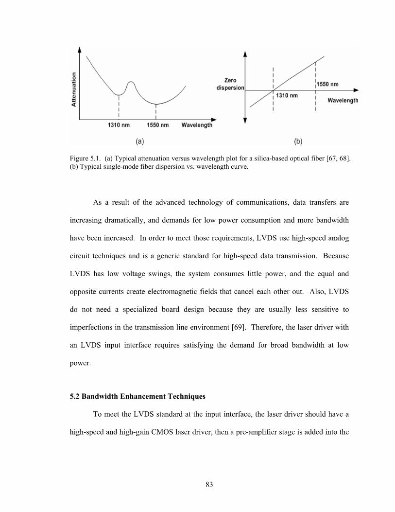
83
Figure 5.1. (a) Typical attenuation versus wavelength plot for a silica-based optical fiber [67, 68]. (b) Typical single-mode fiber dispersion vs. wavelength curve.
As a result of the advanced technology of communications, data transfers are
increasing dramatically, and demands for low power consumption and more bandwidth
have been increased. In order to meet those requirements, LVDS use high-speed analog
circuit techniques and is a generic standard for high-speed data transmission. Because
LVDS has low voltage swings, the system consumes little power, and the equal and
opposite currents create electromagnetic fields that cancel each other out. Also, LVDS
do not need a specialized board design because they are usually less sensitive to
imperfections in the transmission line environment [69]. Therefore, the laser driver with
an LVDS input interface requires satisfying the demand for broad bandwidth at low
power.
5.2 Bandwidth Enhancement Techniques
To meet the LVDS standard at the input interface, the laser driver should have a
high-speed and high-gain CMOS laser driver, then a pre-amplifier stage is added into the

84
current steering output stage of the laser drivers. Here, some useful techniques to
increase bandwidth in CMOS technology are introduced.
5.2.1 Shunt Peaking Technique
Although inductors are commonly used with narrow-band circuits, they are useful
in broadband circuits as well. The idea is to allow the capacitance that limits the
bandwidth to resonate with an inductor, thereby improving the speed. A simple common
source (CS) amplifier is illustrated in Figure 5.2. For simplicity, the parasitic capacitance,
channel length modulation, and body effects are omitted.
The frequency response of this amplifier 5.2 (a) is given as:
RCjRg
VinVout m
ωω
+=
1)( (5.2.1)
When the inductor L is connected in series with a load resistor in the amplifier, which is
called shunt peaking and shown in Figure 5.2 (b), the frequency response of the amplifier
is changed as
( )LCRCj
LjRgVin
Vout m21
)(ωωωω−+
+= (5.2.2)

85
L
C
CM1
VDD
RVout
Vin
VDD
(b)(a)
M1
RVout
Vin
Figure 5.2. Schematics of common source (CS) amplifier with and without shunt peaking.
And it can be written in the form
20
2
0
1
)()0()(
ωωs
Qs
sNAsA++
= (5.2.3)
Then, the Q factor results in
RCLQ = (5.2.4)
The small-signal transfer function (5.2.2) shows a zero at frequency R/L, which
extends the bandwidth of the stage. However, this inductance value can result in
significant gain peaking, which causes signal degradation in broadband applications.
When the value of the Q factor is 0.68, this shunt peaking technique can extend
bandwidth by 78 % without creating any any gain peaking in the amplifier. Thus, when
this technique is applied to laser driver design, the optimized value of inductance should
be used [51, 70]. If chip area is critical, shunt peaking can be implemented by means of

86
an active inductor [51, 71]. Figure 5.4 (a) shows a simplified active inductor using a
transistor and a resistor. Omitting the gate-drain capacitor, body effect, and channel-
length modulation, the small-signal equivalent circuit is illustrated in Figure 5.4 (b).
Then, Zin can be written as
gsm
gs
x
xin SCg
sRCiVsZ
+
+==
1)( (5.2.5)
Therefore, min gZ /1)0( = and RZin =∞)( . For Zin to behave as an inductor, it is
required that R >> mg/1 , then the impedance increases with frequency. However, this
active inductor usually has a headroom problem that requires large supply voltage
technology [71, 72].
Figure 5.3. Frequency response of CS amplifier and shunt peaking.

87
Figure 5.4. (a) Schematic of simplified active inductor. (b) Small-signal equivalent circuit.
5.2.2 Source Degeneration
The bandwidth of a differential amplifier can be widened by including the
resistance and capacitance between sources, as shown in Figure 5.5. This is achieved at
the cost of a reduction in the low-frequency gain. To evaluate the effect of the resistance
and capacitance on frequency response, Figure 5.5 (b) uses the half circuit of a
differential amplifier. Its effective transconductance and voltage gain becomes
( )( )
++
+=
+
=sCRRg
sCRg
sCRg
gGmSSSm
SSm
s
sm
m
121
21
21//
21
(5.2.6)
2/12
1//2
1 sm
m
s
sm
m
RgRdg
Rd
sCR
g
gGmRdAv
+≅
+
== (5.2.7)
The transconductance hence contains a zero at 1/RSCS and a pole at (1+gmRS/2)/(RSCS).

88
If the zero cancels the pole at the drain, RSCS=RDCL, then the amplifier’s overall
bandwidth is increased by a factor of 1+gmRS/2 compared with that of a CS amplifier.
The gain, as mentioned, is decreased by a factor of 1+gmRS/2 at low frequencies [73].
Another advantage of this configuration is that the input pole magnitude seen at the
preceding stage is decreased by a factor of 1+gmRS/2, if RGCGS >> (RSCS+RSCGS/2).
Therefore, the input capacitance is decreased. In addition, the thermal noise of RS may
pose difficulties.
VDD
M2Vin
Rd Rd
CLCL
M1
Rs
Cs
Vout
Rd
CL Vout
Vdd
2Cs
Rs/2
+
Vin
V1
gm1V1
(a) (b)
Figure 5.5. (a) Differential pair with capacitive degeneration. (b) Small-signal model with half circuit.
5.2.3 Cherry-Hooper Topology
The Cherry-Hooper topology is widely used to provide broadband characteristics
with high gain. Figure 5.6 (a) shows a schematic of the circuit topology. The differential
mode half circuit of the amplifier in Figure 5.6 (a) is shown in Figure 5.6 (b). The first

89
differential pair acts as a transconductance stage that converts the input voltage signal
into a current. The current-mode signal then is amplified and converted back into voltage
by a transimpedance stage. The shunt feedback resistor lowers the input impedance of
the transimpedance stage, and provides excellent high-frequency performances. The
input impedance of the transimpedance stage becomes
Dm
FD
in
inin Rg
RRIV
Z11+
+== (5.2.8)
The low-frequency gain is calculated as
( )dm
dm
dm
fdmm
dm
fmdm
in
out
RgRg
RgRRgg
RgRgRg
VV
1
3
1
13
1
13
1111
+−
+=
+
−= (5.2.9)
If 11 >>dm Rg and Rf >> (gm1)-1, then, the gain becomes
fmm
mfm Rg
ggRgAv 3
1
33 ≈−≈ (5.2.10)
The gain is equal to that of a simple common source (CS) stage having a load
resistance of Rf. The pole frequencies of this circuit can be considered approximately as
ωp1 ≈ gm3/C3 and ωp2 ≈ gm1/C2, much higher than those of a CS stage circuit, (RC)-1. Thus,
this topology provides a voltage gain of approximately gm3Rf and high frequency poles.
However, this amplifier encounters headroom problems when it used in low supply
voltage technology. For instance, the minimum supply voltage to the Cherry-Hooper
amplifier equal to
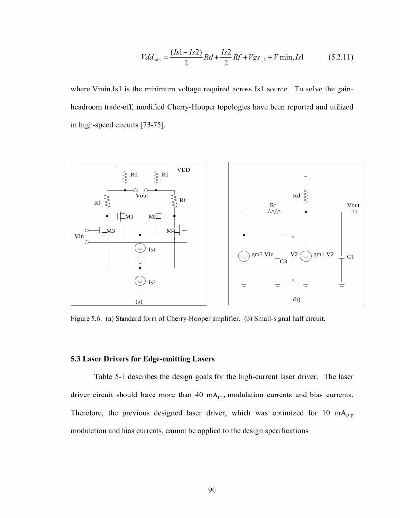
90
1min,22
2)21(
2,1min IsVVgsRfIsRdIsIsVdd ++++
= (5.2.11)
where Vmin,Is1 is the minimum voltage required across Is1 source. To solve the gain-
headroom trade-off, modified Cherry-Hooper topologies have been reported and utilized
in high-speed circuits [73-75].
M4
gm1 V2
Rd
Is2
Is1
Rf Rf
Vin
Vout
VDD
V2 C1gm3 Vin
Rf Vout
C3
Rd
M1
M3
M2
Rd
(b)(a)
Figure 5.6. (a) Standard form of Cherry-Hooper amplifier. (b) Small-signal half circuit.
5.3 Laser Drivers for Edge-emitting Lasers
Table 5-1 describes the design goals for the high-current laser driver. The laser
driver circuit should have more than 40 mAp-p modulation currents and bias currents.
Therefore, the previous designed laser driver, which was optimized for 10 mAp-p
modulation and bias currents, cannot be applied to the design specifications

91
Table 5-1. Design goals for high-current laser driver.
Specification Design Goal
Speed Over 10 Gbps
LVDS input amplitude 100mVp-p
Technology TSMC 0.18 µm CMOS
Output Modulation currents: 40 mAp-p Bias current: 30 mA
It is hard to design the output current switch with LVDS input amplitude of a
maximum 100 mVp-p. Because of this difficulty, the pre-driver stages must be designed
so that the high-gain and high-speed laser driver to interface with LVDS input voltage.
Therefore, the design of the pre-driver should incorporate one of bandwidth enhancement
techniques.
The shunt peaking technique with passive inductors, though it is easily
implemented to increase the bandwidth, was excluded. The reasons for this exclusion are
its requirement of a large chip area, its high parasitic capacitance. In addition, the source
degeneration technique decreases the gain by a factor of 1+gmRS/2, although its
bandwidth increases by the same factor. Instead, this research uses the modified Cherry-
Hooper topology [73-75] and shunt peaking with active inductors to implement the laser
driver.
Figure 5.7 illustrates the gain cells for the pre-driver stage using the modified
Cherry-Hooper topology and the shunt peaking technique with active inductors. To
alleviate gain-headroom problems in the Cherry-Hooper amplifier at low supply voltage,

92
shown in Figure 5.6, the circuit was modified as shown in Figure 5.7(a), where PMOS
loads (M5 and M5) provide part of the bias current of the input differential pair. In
addition, triode-mode PMOS loads (M5, M6, M10, and M11) were used to increase the
gain of the core amplifier because they have better headroom than diode-connected
NMOS loads.
Figure 5.7 (b) depicts the gain cell using the shunt peaking technique with active
inductors. As mentioned in previous sections, the resistance value of PMOS (M6 and
M7) seen by the source should be larger than the 1/gm (M4 and M5) to behave as
inductors. Thus, wide bandwidth operation can be achieved. The overall voltage gain of
the circuit is determined by the size ratio of M1 and M4, where
4
1
)/()/(
41
LWLW
gmgmAv == (5.3.1)
In this design, the approximate voltage gain of 2 was used to avoid bandwidth
degradation caused by Miller capacitance.
The pre-driver circuit’s design started with the optimization of the output current
switch so that it can provide the required currents for laser diodes. Once the current
switch was optimized, the pre-driver stage was designed to have enough bandwidth and
gain with the input impedance of the current switch. After the pre-drivers were
optimized for the given specifications, the current switch was re-optimized to account for
parasitic effects. Overall laser driver schematics are shown in Figure 5.8 and in Figure
5.9. For the pre-driver with shunt peaking, two stages are taped to the left to provide
enough gain and bandwidth.

93
(a)
(b)
Figure 5.7. Schematics of pre-driver stage with (a) modified Cherry-Hooper amplifier. (b) Shunt peaking with active inductors.
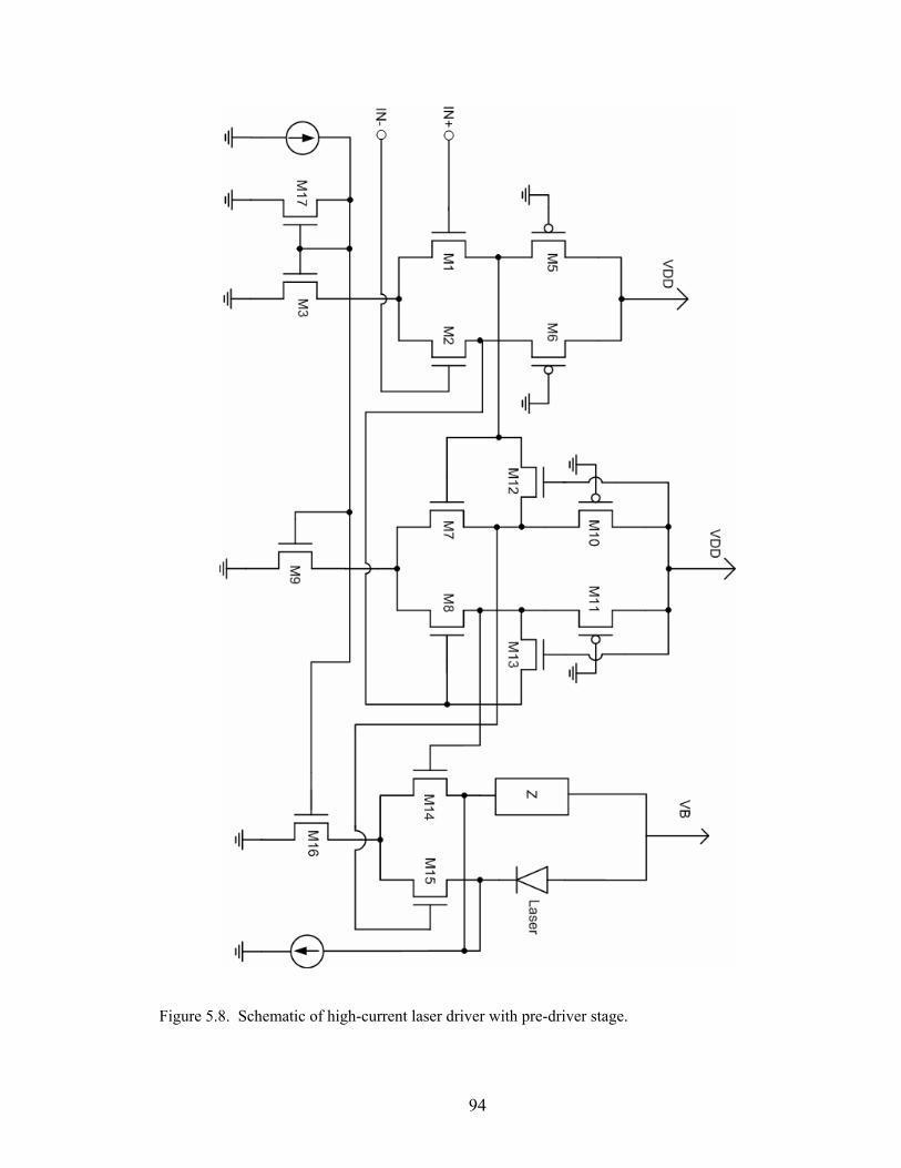
94
Figure 5.8. Schematic of high-current laser driver with pre-driver stage.
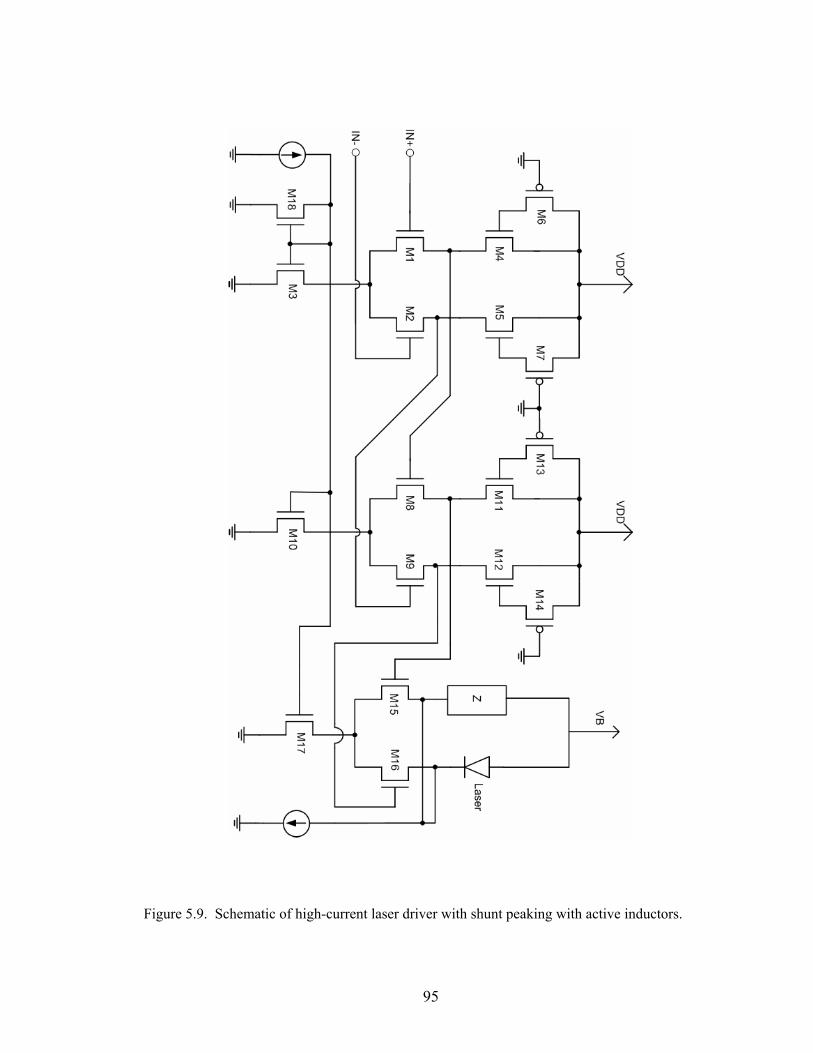
95
Figure 5.9. Schematic of high-current laser driver with shunt peaking with active inductors.
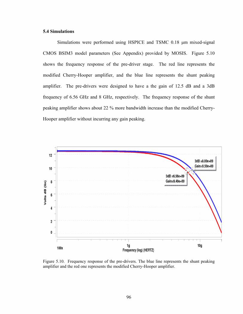
96
5.4 Simulations
Simulations were performed using HSPICE and TSMC 0.18 µm mixed-signal
CMOS BSIM3 model parameters (See Appendix) provided by MOSIS. Figure 5.10
shows the frequency response of the pre-driver stage. The red line represents the
modified Cherry-Hooper amplifier, and the blue line represents the shunt peaking
amplifier. The pre-drivers were designed to have a the gain of 12.5 dB and a 3dB
frequency of 6.56 GHz and 8 GHz, respectively. The frequency response of the shunt
peaking amplifier shows about 22 % more bandwidth increase than the modified Cherry-
Hooper amplifier without incurring any gain peaking.
Figure 5.10. Frequency response of the pre-drivers. The blue line represents the shunt peaking amplifier and the red one represents the modified Cherry-Hooper amplifier.

97
Figure 5.11 illustrates the transient response of the overall laser driver using the
modified Cherry-Hooper amplifier, shown in Figure 5.8 (a), for 10 Gbps operation. The
first trace shows the pulse waveform of input to the pre-driver stage, and the second trace
shows the pulse train of output from the laser driving stage. This trace was shown to
determine if there are missing bits that cannot be easily revealed in an eye diagram. The
last trace shows the eye diagram of output from the laser driver. The eye diagram shows
few jitters at 10 Gbps.
Figure 5.12 shows the transient response of the laser driver using shunt peaking
techniques with active inductors. The first, second, and last trace represent input voltage,
output current, and an eye diagram at 10 Gbps, respectively. As shown in Figure 5.9, this
topology has more bandwidth than the modified Cherry-Hooper amplifier. Therefore, the
eye diagram of output current is clearer.
Based on these simulations, the high-output current laser driver was designed
using bandwidth enhancement techniques. The shunt peaking techniques in the pre-
driver stages have better performance. However, both techniques can be applied to
implement high-output current laser driver because the simulation results meet the
required specifications. More specified circuit performances are summarized in Table 5-
2.

98
Table 5-2. Specified circuit performances.
.
Performance LD with the modified CH LD with active inductors
Speed 10 Gbps 10 Gbps
Input 100mVp-p 100mVp-p
Output Mod: 40mAp-p
Bias: 30mA
Mod: 40mAp-p
Bias: 30mA
Power 694 mW 312 mW
Figure 5.11. Transient response of high-current laser driver using the modified Cherry-Hooper amplifier at 10 Gbps.

99
Figure 5.12. Transient response of high-current laser driver using the shunt peaking with active inductors.

100
CHAPTER VI
CONCLUSIONS AND FUTURE RESEARCH
This chapter covers the contributions associated with the research accomplished
in development of a high-speed optical laser driver using a standard mixed-signal CMOS
process and an optical transmitter with a thin film laser by using the heterogeneous
integration. In addition, future research is addressed.
6.1 Contributions
The laser drivers were implemented for optical data communication using
standard commercial CMOS 0.18 µm technology. These circuits works at up to 10 Gbps
speed with 10-14 BER performance. They are the first digital CMOS laser drivers
developed to date at this speed with low power consumption of 65 mW. Table 6-1 shows
the performance comparison between this laser driver and the recently published lasers.
Moreover, this research was focused to co-design the laser driver and the laser
device. Most circuit designers have focused only on the performance of the circuit itself
without regard to the laser model as they assumed the lasers to be 50 ohm resistors.
However, in this research, all simulations were performed with parasitics extracted from
the layout of circuits and from the packaging models, including bonding wires and test
board traces, to minimize unexpected effects when measurements were performed. In
addition, performance was measured in terms of BER and eye diagrams even though
most of researchers provided only scope captured data or eye-diagrams without BER data.
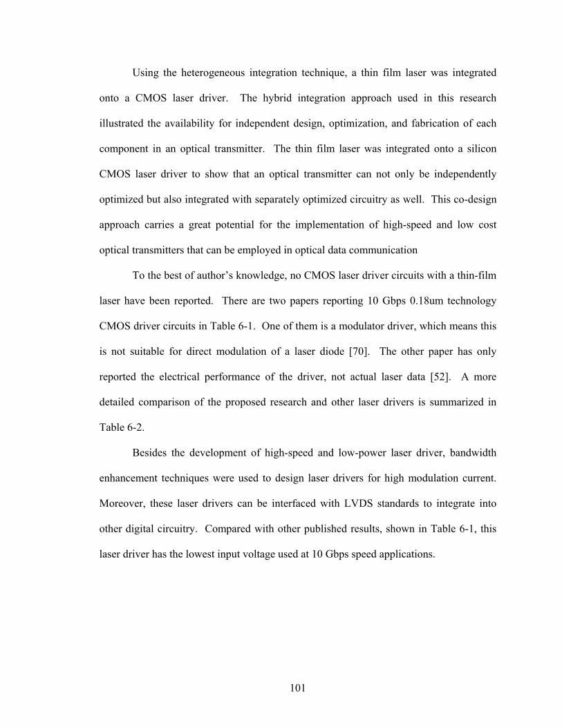
101
Using the heterogeneous integration technique, a thin film laser was integrated
onto a CMOS laser driver. The hybrid integration approach used in this research
illustrated the availability for independent design, optimization, and fabrication of each
component in an optical transmitter. The thin film laser was integrated onto a silicon
CMOS laser driver to show that an optical transmitter can not only be independently
optimized but also integrated with separately optimized circuitry as well. This co-design
approach carries a great potential for the implementation of high-speed and low cost
optical transmitters that can be employed in optical data communication
To the best of author’s knowledge, no CMOS laser driver circuits with a thin-film
laser have been reported. There are two papers reporting 10 Gbps 0.18um technology
CMOS driver circuits in Table 6-1. One of them is a modulator driver, which means this
is not suitable for direct modulation of a laser diode [70]. The other paper has only
reported the electrical performance of the driver, not actual laser data [52]. A more
detailed comparison of the proposed research and other laser drivers is summarized in
Table 6-2.
Besides the development of high-speed and low-power laser driver, bandwidth
enhancement techniques were used to design laser drivers for high modulation current.
Moreover, these laser drivers can be interfaced with LVDS standards to integrate into
other digital circuitry. Compared with other published results, shown in Table 6-1, this
laser driver has the lowest input voltage used at 10 Gbps speed applications.
102
Table 6-1. The performance comparison of the laser driver in this research with others recently published.
Authors Speed Mod. Current
Bias Current Input Etc.
[76] Haralabidis 2.5 Gbps 0~40 mAp-p 0~40 mAp-p 2Vpp 0.8 µm CMOS
[55] Chen, X. 2.5 Gbps 40 mAp-p N/A PECL 0.35 µm CMOS
[77] Annen, R. 500Mbps 2.1 mAp-p N/A tr,tf=82ps
[78] Chan, C.T. 2.5 Gbps 20 mAp-p N/A 0.18 µm CMOS
[51] Chen, G.C. 2.5 Gbps 20 mAp-p 5~10 mAp-p PECL 0.35 µm CMOS
[79] Lin, C.H. 2.5 Gbps 5~20 mAp-p 4~10 mAp-p PECL 0.35 µm CMOS
[52] Petersen, K 10 Gbps 30 mAp-p 40 mAp-p 500mV 0.18 µm CMOS
[70] Cao, J 10 Gbps 8 mAp-p N/A LVDS 0.18 µm CMOS
[54] Calal, S. 10 Gbps 100 mAp-p N/A 800mV 0.18 µm CMOS
Table 6-2. The comparison of proposed laser driver and Peterson’s laser driver.
Speed Mod. Current Input Power Technology
Petersen’s work [52] 10 Gbps 30 mAp-p 500
mVp-p 492.9mW Intel CMOS 0.18
um
This research 10 Gbps 10 mAp-p 800
mVp-p 62.5mW TSMC CMOS 0.18
um
This research 10 Gbps 40 mAp-p 100
mVp-p 312 mW TSMC CMOS 0.18
um

103
6.2 Future Research
This research covers two types of high-speed CMOS laser drivers; low-power
applications and high-modulation current laser drivers of up to 10 Gbps in speed of
operation. However, the implementation of an external modulator driver, which is
widely used in optical communication system, is necessary for future research. To drive
the external modulator, the driver circuitries must provide voltage output instead of the
current output of laser. In addition, the programmable circuitry to compensation for the
variation of laser characteristics because of aging and temperature change is left for
future research. In this research, those effects can be compensated for by manually
adjustment of external current source.
High-speed measurements of the optical transmitter with a thin film laser are one
of the main tasks left to perform. Currently, the thermal properties of the thin film laser
are insufficient for continuous operation. Therefore, to improve upon the work that has
been done for this thesis, the thin film devices with different materials are under
development. Moreover, to improve the light output coupling efficiency of the circuitry,
a micro lens could be integrated on the thin film laser. Finally, the implemented optical
transmitter could be part of an optical transceiver with optical receivers and waveguide.
It will give commercial and government sectors the ability to build a low-cost and high-
speed optoelectronic transceiver that can be employed in chip-to-chip interconnection,
fiber-to-the curb/home/building/desktop, and local area network (LAN) applications.
Other function blocks such as multiplexers to serialize the low-speed parallel
incoming data stream to high-speed signals and to utilize the advantages of
optoelectronics in parallel networks are necessary for future research.

104
6.3. Conclusions
A silicon CMOS laser driver was designed by using differential topology to
minimize unwanted delta I noise and common mode noise. The laser driver was
fabricated by using standard mixed-signal CMOS technology through the MOSIS
foundry under a minimum feature size of 0.18 µm. The performance of this laser driver
has been verified along with BER measurement results and eye diagrams at the data rate
of 10 Gbps non-return-to-zero pseudorandom bit stream (PRBS). Decoupling techniques
are suggested to reduce the effect of parasitics, and the effectiveness of the technique was
verified in simulations and measurements. In addition, the accurate model of parasitic
effects was incorporated in the simulation to predict the actual behavior in the real
measurement environment.
A thin film laser device was integrated onto the silicon CMOS laser driver using
the heterogeneous integration method to create an optical transmitter. This optical
transmitter was tested by a pulsed-mode measurement setup to solve the thermal
problems in the thin film laser. Also, the capability of pulsed-mode test setup was
verified in Chapter IV with an experiment.
In Chapter V, the high-current laser drivers for an LVDS input interface, which is
widely used as a common standard, was introduced. These laser drivers also support a 10
Gbps data rate with a 100 mVp-p input data stream and consist of a differential current
switch and high-speed and high gain pre-driver stages that used the modified Cherry-
Hooper topology and shunt peaking amplifier with active inductors. These laser drivers
will be fabricated and tested.

105
APPENDIX
HSPICE INPUT CONTROL FILES AND BSIM MODELS
A.1 Low Power CMOS Laser Driver Input Control File
*********************************** * * * High Speed Laser Driver Simulations * * * *********************************** .option post list accurate .lib 'models/mm018.l' TT .lib 'models/rf018.l' TT_RFMOS .lib 'models/mm018.l' DIO .inc 'models/PSPLspice.txt' .option cshunt=1e-15 gshunt=1e-12 *********************************** * * * Modified Laser Model * * * *********************************** .param N=3.25 IS=3e-11 IK=1.16e-3 RS=15.78 .model D D(N=N IS=IS IK=IK RS=RS ) .subckt SonyVCSEL 1 2 Lbond 1 L1 0.2n D L1 L11 D L L11 3 0.892n R1 3 4 39.5 C1 3 4 0.04p C2 3 22 0.479p C3 4 22 101p R2 4 22 8.8 Lbond2 22 2 0.2n .ends XVC VDD VCNN Sonyvcsel VM VCNN VCN 0

106
********************************** * * * Electrical Test * * (50 ohm w/ dc block) * * * ********************************** * XRR1 VCN VMR DCB5501 * XRR2 EOUT1 VMD DCB5501 * RVM2 VMR 0 50 * RVM3 VMD 0 50 ********************************** * * * Power Supply * * * ********************************** VESDP ESDVDD 0 3. VESDN ESDVSS 0 0 VDD VDDP 0 3. VSS VSSP 0 0 LVDD VDDP VDD 15.2n LVSS VSSP VSS 15.2n ********************************** * * * Bias and modulation currents * * * ********************************** .param biasN=0.3m imod=3m Ibiasn VSS IBIAS biasN Imod VSS IMOD imod ********************************** * * * input * * * ********************************** .param imid1=1.5 imid2=1.5 .param tt=.10ns Ihigh1=imid1+.4 +Ilow1=imid1-0.4 slope1=0.020ns .param tt=.10ns Ihigh2=imid2+.4 +Ilow2=imid2-0.4 slope2=0.020ns .inc 'ldu.in'
107
********************************** * * * Analysis * * * ********************************** .op * .trans .005ns 80n .ac DEC 1000 100Mega 20giga .probe i1(d166) .incl 'LD_U_Cinc.ext' *.inc 'tsmc_ch_u.ext' .END ********************************** * * * ldu.in files * * * ********************************** CIN1 innn inn 0.01u *Xcin1 innn inn cd BT5580 Rin1 101 INNn 0 VIin 101 VSS ac 1 pwl + 0 Imid1, 'tt-slope1' Imid1, + 'tt' Ilow1, 'tt*3-slope1' Ilow1, + 'tt*3' Ihigh1, 'tt*4-slope1' Ihigh1, + 'tt*4' Ilow1, 'tt*5-slope1' Ilow1, + 'tt*5' Ihigh1, 'tt*8-slope1' Ihigh1, + 'tt*8' Ilow1, 'tt*15-slope1' Ilow1, + 'tt*15' Ihigh1, 'tt*17-slope1' Ihigh1, + 'tt*17' Ilow1, 'tt*18-slope1' Ilow1, + 'tt*18' Ihigh1, 'tt*19-slope1' Ihigh1, + 'tt*19' Ilow1, 'tt*22-slope1' Ilow1, + 'tt*22' Ihigh1, 'tt*27-slope1' Ihigh1, + 'tt*27' Ilow1, 'tt*28-slope1' Ilow1, + 'tt*28' Ihigh1, 'tt*29-slope1' Ihigh1, + 'tt*29' Ilow1, 'tt*30-slope1' Ilow1, + 'tt*30' Ihigh1, 'tt*36-slope1' Ihigh1, + 'tt*36' Ilow1, 'tt*39-slope1' Ilow1, + 'tt*39' Ihigh1, 'tt*40-slope1' Ihigh1, + 'tt*40' Ilow1, 'tt*41-slope1' Ilow1, + 'tt*41' Ihigh1, 'tt*42-slope1' Ihigh1, + 'tt*42' Ilow1, 'tt*49-slope1' Ilow1, + 'tt*49' Ihigh1, 'tt*50-slope1' Ihigh1, + 'tt*50' Ilow1, 'tt*57-slope1' Ilow1, + 'tt*57' Ihigh1, 'tt*64-slope1' Ihigh1, + 'tt*64' Ilow1, 'tt*65-slope1' Ilow1, + 'tt*65' Ihigh1, 'tt*72-slope1' Ihigh1, + 'tt*72' Ilow1, 'tt*73-slope1' Ilow1, + 'tt*73' Ihigh1, 'tt*74-slope1' Ihigh1, + 'tt*74' Ilow1, 'tt*75-slope1' Ilow1, + 'tt*75' Ihigh1, 'tt*78-slope1' Ihigh1,

108
+ 'tt*78' Ilow1, 'tt*85-slope1' Ilow1, + 'tt*85' Ihigh1, 'tt*87-slope1' Ihigh1, + 'tt*87' Ilow1, 'tt*88-slope1' Ilow1, + 'tt*88' Ihigh1, 'tt*89-slope1' Ihigh1, + 'tt*89' Ilow1, 'tt*92-slope1' Ilow1, + 'tt*92' Ihigh1, 'tt*97-slope1' Ihigh1, + 'tt*97' Ilow1, 'tt*98-slope1' Ilow1, + 'tt*98' Ihigh1, 'tt*99-slope1' Ihigh1, + 'tt*99' Ilow1, 'tt*100-slope1' Ilow1, + 'tt*100' Ihigh1, 'tt*106-slope1' Ihigh1, + 'tt*106' Ilow1, 'tt*109-slope1' Ilow1, + 'tt*109' Ihigh1, 'tt*110-slope1' Ihigh1, + 'tt*110' Ilow1, 'tt*111-slope1' Ilow1, + 'tt*111' Ihigh1, 'tt*112-slope1' Ihigh1, + 'tt*112' Ilow1, R 'tt' * Xcin2 inpp inp ab BT5580 Cin2 201 INP 0.01u VIin2 201 VSS ac 1 pwl + 0 Imid2, 'tt-slope2' Imid2, + 'tt' Ihigh2, 'tt*3-slope2' Ihigh2, + 'tt*3' Ilow2, 'tt*4-slope2' Ilow2, + 'tt*4' Ihigh2, 'tt*5-slope2' Ihigh2, + 'tt*5' Ilow2, 'tt*8-slope2' Ilow2, + 'tt*8' Ihigh2, 'tt*15-slope2' Ihigh2, + 'tt*15' Ilow2, 'tt*17-slope2' Ilow2, + 'tt*17' Ihigh2, 'tt*18-slope2' Ihigh2, + 'tt*18' Ilow2, 'tt*19-slope2' Ilow2, + 'tt*19' Ihigh2, 'tt*22-slope2' Ihigh2, + 'tt*22' Ilow2, 'tt*27-slope2' Ilow2, + 'tt*27' Ihigh2, 'tt*28-slope2' Ihigh2, + 'tt*28' Ilow2, 'tt*29-slope2' Ilow2, + 'tt*29' Ihigh2, 'tt*30-slope2' Ihigh2, + 'tt*30' Ilow2, 'tt*36-slope2' Ilow2, + 'tt*36' Ihigh2, 'tt*39-slope2' Ihigh2, + 'tt*39' Ilow2, 'tt*40-slope2' Ilow2, + 'tt*40' Ihigh2, 'tt*41-slope2' Ihigh2, + 'tt*41' Ilow2, 'tt*42-slope2' Ilow2, + 'tt*42' Ihigh2, 'tt*49-slope2' Ihigh2, + 'tt*49' Ilow2, 'tt*50-slope2' Ilow2, + 'tt*50' Ihigh2, 'tt*57-slope2' Ihigh2, + 'tt*57' Ilow2, 'tt*64-slope2' Ilow2, + 'tt*64' Ihigh2, 'tt*65-slope2' Ihigh2, + 'tt*65' Ilow2, 'tt*72-slope2' Ilow2, + 'tt*72' Ihigh2, 'tt*73-slope2' Ihigh2, + 'tt*73' Ilow2, 'tt*74-slope2' Ilow2, + 'tt*74' Ihigh2, 'tt*75-slope2' Ihigh2, + 'tt*75' Ilow2, 'tt*78-slope2' Ilow2, + 'tt*78' Ihigh2, 'tt*85-slope2' Ihigh2, + 'tt*85' Ilow2, 'tt*87-slope2' Ilow2,

109
+ 'tt*87' Ihigh2, 'tt*88-slope2' Ihigh2, + 'tt*88' Ilow2, 'tt*89-slope2' Ilow2, + 'tt*89' Ihigh2, 'tt*92-slope2' Ihigh2, + 'tt*92' Ilow2, 'tt*97-slope2' Ilow2, + 'tt*97' Ihigh2, 'tt*98-slope2' Ihigh2, + 'tt*98' Ilow2, 'tt*99-slope2' Ilow2, + 'tt*99' Ihigh2, 'tt*100-slope2' Ihigh2, + 'tt*100' Ilow2, 'tt*106-slope2' Ilow2, + 'tt*106' Ihigh2, 'tt*109-slope2' Ihigh2, + 'tt*109' Ilow2, 'tt*110-slope2' Ilow2, + 'tt*110' Ihigh2, 'tt*111-slope2' Ihigh2, + 'tt*111' Ilow2, 'tt*112-slope2' Ilow2, + 'tt*112' Ihigh2, R 'tt' Veye eye 0 + pulse 0 1 0n '3*tt-slope1/100000' 'slope1/100000' 0n '3*tt' Reye eye 0 1T ********************************** * * * PSPLspice.txt * * * *********************************** .SUBCKT DCB5501 1 2 * Subcircuit for PSPL model 5501A DC Block * 0.22uF, 50V, 7kHz - >26GHz * J.R.Andrews, PSPL, 7/30/01 * This is NOT the actual circuit -- but a * phenomological model. Model not valid for * f > 25GHz. Good approx. for IL & RL C1 1 3 0.22UF * ; -50%,+80% TOLERANCE R1 3 4 6 L1 3 4 0.18NH R2 4 5 7 L2 4 5 0.2NH C2 4 5 14PF R3 5 2 270 L3 5 2 10PH C3 5 2 3.75PF .ENDS * * .SUBCKT BT5580 1 2 3 * Subcircuit for PSPL model 5580 bias tee * 0.22uF,50V,1mH,1 Amp,0.8ohm,10kHz-15GHz * J.R.Andrews, PSPL, 8/4/01 * This is NOT the actual circuit -- but a

110
* phenomological model. Model not valid for * f > 20GHz. Good approx. for IL & RL * node 1 is AC port, node 2 is AC+DC port * node 3 is DC port C1 1 6 0.22UF * ; -50%, +80%% TOLERANCE Rdc 6 4 0.8 L1 4 3 1.1MH * ; +-25% TOLERANCE R1 4 3 3.3K R2 6 5 220 C2 5 0 0.05UF R3 6 7 180 L3 7 8 33NH C3 8 0 30FF R4 6 9 110 L4 9 10 4.7NH C4 10 0 43FF R5 6 11 150 L5 11 12 3.3NH C5 12 0 27FF C6 6 0 0.29PF L6 6 2 0.72NH C7 2 0 0.29PF .ENDS
A.2 High Current Laser Driver Input Control Files
.option post list
.option relv=1e-4 relvar=1e-2 .lib '~/research/SONY/models/mm018.l' TT .param imid1=1.25 imid2=1.25 .param tt=.10ns Ihigh1=imid1+.05 Ilow1=imid1-0.05 slope1=0.050ns .param tt=.10ns Ihigh2=imid2+.05 Ilow2=imid2-0.05 slope2=0.050ns .inc 'os_input.l' .inc 'CH_LD1.ext' .op .tran 0.002n 10n .end .option post list .option relv=1e-4 relvar=1e-2 .lib '~/research/SONY/models/mm018.l' TT .param imid1=1.2 imid2=1.2 .param tt=.10ns Ihigh1=imid1+.05 Ilow1=imid1-0.05 slope1=0.050ns

111
.param tt=.10ns Ihigh2=imid2+.05 Ilow2=imid2-0.05 slope2=0.050ns .inc 'os_input.l' .inc 'AI_LD1.ext' .op .probe dbgain=par('db(V(out1))') .tran 0.002n 8n .end
A.3 Laser Driver Netlist File
X8 VDD VSS MIMCAP LT=29.9999992421363E-6 M=1.0 X10 VDD VSS MIMCAP LT=29.9999992421363E-6 M=1.0 X12 VDD VSS MIMCAP LT=29.9999992421363E-6 M=1.0 X14 VDD VSS MIMCAP LT=29.9999992421363E-6 M=1.0 X16 VDD VSS MIMCAP LT=29.9999992421363E-6 M=1.0 X18 VDD VSS MIMCAP LT=29.9999992421363E-6 M=1.0 X20 VDD VSS MIMCAP LT=29.9999992421363E-6 M=1.0 X22 VDD VSS MIMCAP LT=29.9999992421363E-6 M=1.0 X24 VDD VSS MIMCAP LT=29.9999992421363E-6 M=1.0 X26 VDD VSS MIMCAP LT=29.9999992421363E-6 M=1.0 X28 VDD VSS MIMCAP LT=29.9999992421363E-6 M=1.0 X30 VDD VSS MIMCAP LT=29.9999992421363E-6 M=1.0 X32 VDD VSS MIMCAP LT=29.9999992421363E-6 M=1.0 X34 VDD VSS MIMCAP LT=29.9999992421363E-6 M=1.0 X36 VDD VSS MIMCAP LT=29.9999992421363E-6 M=1.0 X38 VDD VSS MIMCAP LT=29.9999992421363E-6 M=1.0 X40 VDD VSS MIMCAP LT=29.9999992421363E-6 M=1.0 X42 VDD VSS MIMCAP LT=29.9999992421363E-6 M=1.0 X44 VDD VSS MIMCAP LT=29.9999992421363E-6 M=1.0 X46 VDD VSS MIMCAP LT=29.9999992421363E-6 M=1.0 X48 VDD VSS MIMCAP LT=29.9999992421363E-6 M=1.0 X50 VDD VSS MIMCAP LT=29.9999992421363E-6 M=1.0 X52 VDD VSS MIMCAP LT=29.9999992421363E-6 M=1.0 X54 VDD VSS MIMCAP LT=29.9999992421363E-6 M=1.0 X56 VDD VSS MIMCAP LT=29.9999992421363E-6 M=1.0 X58 VDD VSS MIMCAP LT=29.9999992421363E-6 M=1.0 X60 VDD VSS MIMCAP LT=29.9999992421363E-6 M=1.0 X62 VDD VSS MIMCAP LT=29.9999992421363E-6 M=1.0 X64 VDD VSS MIMCAP LT=29.9999992421363E-6 M=1.0 X66 VDD VSS MIMCAP LT=29.9999992421363E-6 M=1.0 X68 VDD VSS MIMCAP LT=29.9999992421363E-6 M=1.0 X70 VDD VSS MIMCAP LT=29.9999992421363E-6 M=1.0 X72 VDD VSS MIMCAP LT=29.9999992421363E-6 M=1.0 X74 VDD VSS MIMCAP LT=29.9999992421363E-6 M=1.0 X76 VDD VSS MIMCAP LT=29.9999992421363E-6 M=1.0 X78 VDD VSS MIMCAP LT=29.9999992421363E-6 M=1.0 X80 VDD VSS MIMCAP LT=29.9999992421363E-6 M=1.0 X82 VDD VSS MIMCAP LT=29.9999992421363E-6 M=1.0

112
X84 VDD VSS MIMCAP LT=29.9999992421363E-6 M=1.0 X86 VDD VSS MIMCAP LT=29.9999992421363E-6 M=1.0 X88 VDD VSS MIMCAP LT=29.9999992421363E-6 M=1.0 X90 VDD VSS MIMCAP LT=29.9999992421363E-6 M=1.0 X92 VDD VSS MIMCAP LT=29.9999992421363E-6 M=1.0 X94 VDD VSS MIMCAP LT=29.9999992421363E-6 M=1.0 X96 VDD VSS MIMCAP LT=29.9999992421363E-6 M=1.0 X98 VDD VSS MIMCAP LT=29.9999992421363E-6 M=1.0 X100 VDD VSS MIMCAP LT=29.9999992421363E-6 M=1.0 X10² VDD VSS MIMCAP LT=29.9999992421363E-6 M=1.0 X10⁴ VDD VSS MIMCAP LT=29.9999992421363E-6 M=1.0 X10⁶ VDD VSS MIMCAP LT=29.9999992421363E-6 M=1.0 X10⁸ VDD VSS MIMCAP LT=29.9999992421363E-6 M=1.0 X110 VDD VSS MIMCAP LT=29.9999992421363E-6 M=1.0 X112 VDD VSS MIMCAP LT=29.9999992421363E-6 M=1.0 X114 VDD VSS MIMCAP LT=29.9999992421363E-6 M=1.0 X116 VDD VSS MIMCAP LT=29.9999992421363E-6 M=1.0 X118 VDD VSS MIMCAP LT=29.9999992421363E-6 M=1.0 X120 VDD VSS MIMCAP LT=29.9999992421363E-6 M=1.0 X122 VDD VSS MIMCAP LT=29.9999992421363E-6 M=1.0 X124 VDD VSS MIMCAP LT=29.9999992421363E-6 M=1.0 X126 VDD VSS MIMCAP LT=29.9999992421363E-6 M=1.0 X128 VDD VSS MIMCAP LT=29.9999992421363E-6 M=1.0 X130 VDD VSS MIMCAP LT=29.9999992421363E-6 M=1.0 X132 VDD VSS MIMCAP LT=29.9999992421363E-6 M=1.0 X134 VDD VSS MIMCAP LT=29.9999992421363E-6 M=1.0 X136 VDD VSS MIMCAP LT=29.9999992421363E-6 M=1.0 X138 VDD VSS MIMCAP LT=29.9999992421363E-6 M=1.0 X140 VDD VSS MIMCAP LT=29.9999992421363E-6 M=1.0 X142 VDD VSS MIMCAP LT=29.9999992421363E-6 M=1.0 X144 VDD VSS MIMCAP LT=29.9999992421363E-6 M=1.0 X146 VDD VSS MIMCAP LT=29.9999992421363E-6 M=1.0 X148 VDD VSS MIMCAP LT=29.9999992421363E-6 M=1.0 X150 VDD VSS MIMCAP LT=29.9999992421363E-6 M=1.0 X152 VDD VSS MIMCAP LT=29.9999992421363E-6 M=1.0 X154 VDD VSS MIMCAP LT=29.9999992421363E-6 M=1.0 X156 VDD VSS MIMCAP LT=29.9999992421363E-6 M=1.0 X158 VDD VSS MIMCAP LT=29.9999992421363E-6 M=1.0 X160 VDD VSS MIMCAP LT=29.9999992421363E-6 M=1.0 X162 VDD VSS MIMCAP LT=29.9999992421363E-6 M=1.0 D164 VDD 6 PDIO AREA=100.000001335143E-12 PJ=39.999998989515E-6 W=10E-6 +L=10E-6 M=1.0 D166 6 EOUT1 PDIO AREA=100.000001335143E-12 PJ=39.999998989515E-6 W=10E-6 +L=10E-6 M=1.0 X168 VCN1 VDD RNODWO_RF W=1.99999999495049E-6 L=9.99999974737875E-6 X170 VCN1 VDD RNODWO_RF W=1.99999999495049E-6 L=9.99999974737875E-6 X172 VCN1 VDD RNODWO_RF W=1.99999999495049E-6 L=9.99999974737875E-6 X174 VCN1 VDD RNODWO_RF W=1.99999999495049E-6 L=9.99999974737875E-6 X176 INN INP RNODWO_RF W=1.99999999495049E-6 L=9.99999974737875E-6

113
X178 INN INP RNODWO_RF W=1.99999999495049E-6 L=9.99999974737875E-6 X180 INN INP RNODWO_RF W=1.99999999495049E-6 L=9.99999974737875E-6 X182 INN INP RNODWO_RF W=1.99999999495049E-6 L=9.99999974737875E-6 X184 VSS 2 RPPOLYHRI_RF W=1.99999999495049E-6 L=9.99999974737875E-6 X186 VSS 3 RPPOLYHRI_RF W=1.99999999495049E-6 L=9.99999974737875E-6 C664 4 5 1.03871089162467E-15 C666 3 5 690.78009126003E-18 C668 2 4 690.287488661642E-18 C670 2 3 13.7252482582342E-18 C672 VSS 5 45.0840565365492E-18 C674 VSS 4 45.3158193092967E-18 C676 VSS 3 401.225345782275E-18 C678 VSS 2 401.615245635808E-18 C680 VSS 1 5.25573017046274E-15 C682 INP 5 131.974284452671E-18 C684 INP 4 1.41759359937097E-15 C686 INP 2 534.359840379558E-18 C688 INP 1 11.3420659312007E-15 C690 INP VSS 128.195915796887E-15 C692 INN 5 1.34718335035574E-15 C694 INN 4 77.9691710365215E-18 C696 INN 3 533.223280983021E-18 C698 INN 1 11.7252390725831E-15 C700 INN VSS 128.136230467292E-15 C702 INN INP 6.86522533090215E-15 C704 IBIAS VSS 9.2133560912369E-15 C706 ESDVDD VSS 69.0966313571066E-15 C708 ESDVDD IBIAS 69.1306346477412E-15 C710 ESDVSS 6 301.628803094171E-18 C712 ESDVSS 5 334.915927371844E-18 C714 ESDVSS 4 334.0256692745E-18 C716 ESDVSS 3 1.09336389260124E-15 C718 ESDVSS 2 1.09454359773853E-15 C720 ESDVSS 1 11.3125713969444E-15 C722 ESDVSS VSS 2.56253308503207E-12 C724 ESDVSS INP 82.273035227013E-15 C726 ESDVSS INN 81.2539190661946E-15 C728 ESDVSS IBIAS 456.823869097317E-15 C730 ESDVSS ESDVDD 940.104981708711E-15 C732 IMOD 1 5.55646455970417E-15 C734 IMOD VSS 9.1175041488597E-15 C736 IMOD ESDVDD 69.0966313571066E-15 C738 IMOD ESDVSS 477.675841589753E-15 C740 EOUT1 6 8.73521615690721E-15 C742 EOUT1 1 24.9660098231843E-15 C744 EOUT1 VSS 131.128452280499E-15 C746 EOUT1 INP 5.40451193116443E-15 C748 EOUT1 INN 44.3092695439953E-18 C750 EOUT1 IBIAS 714.694848915893E-18 C752 EOUT1 ESDVSS 87.1222785212532E-15 C754 EOUT1 IMOD 3.15265239451577E-15

114
C756 VDD 6 3.71514961061193E-15 C758 VDD 5 4.75281452242586E-15 C760 VDD 4 3.37628200984335E-15 C762 VDD 3 585.80893923314E-18 C764 VDD VSS 13.3640801129966E-15 C766 VDD INP 1.98630094339904E-15 C768 VDD INN 3.30970627898035E-15 C770 VDD ESDVDD 138.227360872538E-15 C772 VDD ESDVSS 1.14113406224359E-12 C774 VDD IMOD 12.615429195533E-15 C776 VDD EOUT1 3.47657960464421E-15 C778 VCN 1 22.8936285212459E-15 C780 VCN VSS 130.633161623053E-15 C782 VCN INP 18.0732644182957E-18 C784 VCN INN 5.41046233761889E-15 C786 VCN IBIAS 1.27007476479363E-15 C788 VCN ESDVSS 96.2127445314036E-15 C790 VCN IMOD 651.111367818184E-18 C792 VCN EOUT1 896.680724666427E-18 * Include files * End of Netlist M188 VDD 5 INN VDD PCH L=180.000000682412E-9 W=1.99999999495049E-6 +AD=959.999983153603E-15 AS=540.000010852693E-15 PD=4.95999984195805E-6 +PS=2.53999996857601E-6 M=+1.00000000E+00 M190 VDD 4 INP VDD PCH L=180.000000682412E-9 W=1.99999999495049E-6 +AD=959.999983153603E-15 AS=540.000010852693E-15 PD=4.95999984195805E-6 +PS=2.53999996857601E-6 M=+1.00000000E+00 M192 INN 5 VDD VDD PCH L=180.000000682412E-9 W=1.99999999495049E-6 +AD=540.000010852693E-15 AS=540.000010852693E-15 PD=2.53999996857601E-6 +PS=2.53999996857601E-6 M=+1.00000000E+00 M194 INP 4 VDD VDD PCH L=180.000000682412E-9 W=1.99999999495049E-6 +AD=540.000010852693E-15 AS=540.000010852693E-15 PD=2.53999996857601E-6 +PS=2.53999996857601E-6 M=+1.00000000E+00 M196 VDD 5 INN VDD PCH L=180.000000682412E-9 W=1.99999999495049E-6 +AD=540.000010852693E-15 AS=540.000010852693E-15 PD=2.53999996857601E-6 +PS=2.53999996857601E-6 M=+1.00000000E+00 M198 VDD 4 INP VDD PCH L=180.000000682412E-9 W=1.99999999495049E-6 +AD=540.000010852693E-15 AS=540.000010852693E-15 PD=2.53999996857601E-6 +PS=2.53999996857601E-6 M=+1.00000000E+00 M200 INP 4 VDD VDD PCH L=180.000000682412E-9 W=1.99999999495049E-6 +AD=540.000010852693E-15 AS=540.000010852693E-15 PD=2.53999996857601E-6 +PS=2.53999996857601E-6 M=+1.00000000E+00 M202 INN 5 VDD VDD PCH L=180.000000682412E-9 W=1.99999999495049E-6 +AD=540.000010852693E-15 AS=540.000010852693E-15 PD=2.53999996857601E-6 +PS=2.53999996857601E-6 M=+1.00000000E+00 M204 VDD 5 INN VDD PCH L=180.000000682412E-9 W=1.99999999495049E-6 +AD=540.000010852693E-15 AS=959.999983153603E-15 PD=2.53999996857601E-6 +PS=4.95999984195805E-6 M=+1.00000000E+00 M206 VDD 4 INP VDD PCH L=180.000000682412E-9 W=1.99999999495049E-6 +AD=540.000010852693E-15 AS=959.999983153603E-15 PD=2.53999996857601E-6

115
+PS=4.95999984195805E-6 M=+1.00000000E+00 M208 5 5 VDD VDD PCH L=180.000000682412E-9 W=2.00499994207348E-6 +AD=962.399973082617E-15 AS=541.350005187763E-15 PD=4.9700001909514E-6 +PS=2.54499991569901E-6 M=+1.00000000E+00 M210 4 4 VDD VDD PCH L=180.000000682412E-9 W=2.00499994207348E-6 +AD=962.399973082617E-15 AS=541.350005187763E-15 PD=4.9700001909514E-6 +PS=2.54499991569901E-6 M=+1.00000000E+00 M212 VDD 5 5 VDD PCH L=180.000000682412E-9 W=2.00499994207348E-6 +AD=541.350005187763E-15 AS=962.399973082617E-15 PD=2.54499991569901E-6 +PS=4.9700001909514E-6 M=+1.00000000E+00 M214 VDD 4 4 VDD PCH L=180.000000682412E-9 W=2.00499994207348E-6 +AD=541.350005187763E-15 AS=962.399973082617E-15 PD=2.54499991569901E-6 +PS=4.9700001909514E-6 M=+1.00000000E+00 M216 IMOD IMOD VSS ESDVSS NCH L=180.000000682412E-9 W=3.00000010611257E-6 +AD=1.44000002894051E-12 AS=810.000016279039E-15 PD=6.96000006428221E-6 +PS=3.54000007973809E-6 M=+1.00000000E+00 M218 VSS IMOD IMOD ESDVSS NCH L=180.000000682412E-9 W=3.00000010611257E-6 +AD=810.000016279039E-15 AS=810.000016279039E-15 PD=3.54000007973809E-6 +PS=3.54000007973809E-6 M=+1.00000000E+00 M220 IMOD IMOD VSS ESDVSS NCH L=180.000000682412E-9 W=3.00000010611257E-6 +AD=810.000016279039E-15 AS=810.000016279039E-15 PD=3.54000007973809E-6 +PS=3.54000007973809E-6 M=+1.00000000E+00 M222 VSS IMOD IMOD ESDVSS NCH L=180.000000682412E-9 W=3.00000010611257E-6 +AD=810.000016279039E-15 AS=810.000016279039E-15 PD=3.54000007973809E-6 +PS=3.54000007973809E-6 M=+1.00000000E+00 M224 IMOD IMOD VSS ESDVSS NCH L=180.000000682412E-9 W=3.00000010611257E-6 +AD=810.000016279039E-15 AS=1.44000002894051E-12 PD=3.54000007973809E-6 +PS=6.96000006428221E-6 M=+1.00000000E+00 M226 5 INN 3 ESDVSS NCH L=180.000000682412E-9 W=1.83500003458903E-6 +AD=880.799990235492E-15 AS=495.449980954937E-15 PD=4.63000014860881E-6 +PS=2.37499989452772E-6 M=+1.00000000E+00 M228 4 INP 2 ESDVSS NCH L=180.000000682412E-9 W=1.83500003458903E-6 +AD=880.799990235492E-15 AS=495.449980954937E-15 PD=4.63000014860881E-6 +PS=2.37499989452772E-6 M=+1.00000000E+00 M230 3 INN 5 ESDVSS NCH L=180.000000682412E-9 W=1.83500003458903E-6 +AD=495.449980954937E-15 AS=495.449980954937E-15 PD=2.37499989452772E-6 +PS=2.37499989452772E-6 M=+1.00000000E+00 M232 2 INP 4 ESDVSS NCH L=180.000000682412E-9 W=1.83500003458903E-6 +AD=495.449980954937E-15 AS=495.449980954937E-15 PD=2.37499989452772E-6 +PS=2.37499989452772E-6 M=+1.00000000E+00 M234 5 INN 3 ESDVSS NCH L=180.000000682412E-9 W=1.83500003458903E-6 +AD=495.449980954937E-15 AS=880.799990235492E-15 PD=2.37499989452772E-6 +PS=4.63000014860881E-6 M=+1.00000000E+00 M236 4 INP 2 ESDVSS NCH L=180.000000682412E-9 W=1.83500003458903E-6 +AD=495.449980954937E-15 AS=880.799990235492E-15 PD=2.37499989452772E-6 +PS=4.63000014860881E-6 M=+1.00000000E+00 M238 1 INP EOUT1 ESDVSS NCH L=180.000000682412E-9 W=1.09999996311672E-6 +AD=297.00000054797E-15 AS=297.00000054797E-15 PD=1.64000005042908E-6 +PS=1.64000005042908E-6 M=+1.00000000E+00 M240 EOUT1 INP 1 ESDVSS NCH L=180.000000682412E-9 W=1.09999996311672E-6 +AD=297.00000054797E-15 AS=528.000006997514E-15 PD=1.64000005042908E-6

116
+PS=3.16000000566419E-6 M=+1.00000000E+00 M242 EOUT1 INP 1 ESDVSS NCH L=180.000000682412E-9 W=1.09999996311672E-6 +AD=297.00000054797E-15 AS=297.00000054797E-15 PD=1.64000005042908E-6 +PS=1.64000005042908E-6 M=+1.00000000E+00 M244 1 INP EOUT1 ESDVSS NCH L=180.000000682412E-9 W=1.09999996311672E-6 +AD=528.000006997514E-15 AS=297.00000054797E-15 PD=3.16000000566419E-6 +PS=1.64000005042908E-6 M=+1.00000000E+00 M246 1 INP EOUT1 ESDVSS NCH L=180.000000682412E-9 W=1.09999996311672E-6 +AD=297.00000054797E-15 AS=528.000006997514E-15 PD=1.64000005042908E-6 +PS=3.16000000566419E-6 M=+1.00000000E+00 M248 EOUT1 INP 1 ESDVSS NCH L=180.000000682412E-9 W=1.09999996311672E-6 +AD=297.00000054797E-15 AS=297.00000054797E-15 PD=1.64000005042908E-6 +PS=1.64000005042908E-6 M=+1.00000000E+00 M250 1 INP EOUT1 ESDVSS NCH L=180.000000682412E-9 W=1.09999996311672E-6 +AD=297.00000054797E-15 AS=297.00000054797E-15 PD=1.64000005042908E-6 +PS=1.64000005042908E-6 M=+1.00000000E+00 M252 EOUT1 INP 1 ESDVSS NCH L=180.000000682412E-9 W=1.09999996311672E-6 +AD=297.00000054797E-15 AS=297.00000054797E-15 PD=1.64000005042908E-6 +PS=1.64000005042908E-6 M=+1.00000000E+00 M254 1 INP EOUT1 ESDVSS NCH L=180.000000682412E-9 W=1.09999996311672E-6 +AD=297.00000054797E-15 AS=528.000006997514E-15 PD=1.64000005042908E-6 +PS=3.16000000566419E-6 M=+1.00000000E+00 M256 EOUT1 INP 1 ESDVSS NCH L=180.000000682412E-9 W=1.09999996311672E-6 +AD=528.000006997514E-15 AS=297.00000054797E-15 PD=3.16000000566419E-6 +PS=1.64000005042908E-6 M=+1.00000000E+00 M258 1 INP EOUT1 ESDVSS NCH L=180.000000682412E-9 W=1.09999996311672E-6 +AD=297.00000054797E-15 AS=297.00000054797E-15 PD=1.64000005042908E-6 +PS=1.64000005042908E-6 M=+1.00000000E+00 M260 EOUT1 INP 1 ESDVSS NCH L=180.000000682412E-9 W=1.09999996311672E-6 +AD=297.00000054797E-15 AS=297.00000054797E-15 PD=1.64000005042908E-6 +PS=1.64000005042908E-6 M=+1.00000000E+00 M262 1 INP EOUT1 ESDVSS NCH L=180.000000682412E-9 W=1.09999996311672E-6 +AD=297.00000054797E-15 AS=297.00000054797E-15 PD=1.64000005042908E-6 +PS=1.64000005042908E-6 M=+1.00000000E+00 M264 EOUT1 INP 1 ESDVSS NCH L=180.000000682412E-9 W=1.09999996311672E-6 +AD=297.00000054797E-15 AS=528.000006997514E-15 PD=1.64000005042908E-6 +PS=3.16000000566419E-6 M=+1.00000000E+00 M266 1 INP EOUT1 ESDVSS NCH L=180.000000682412E-9 W=1.09999996311672E-6 +AD=528.000006997514E-15 AS=297.00000054797E-15 PD=3.16000000566419E-6 +PS=1.64000005042908E-6 M=+1.00000000E+00 M268 EOUT1 INP 1 ESDVSS NCH L=180.000000682412E-9 W=1.09999996311672E-6 +AD=297.00000054797E-15 AS=297.00000054797E-15 PD=1.64000005042908E-6 +PS=1.64000005042908E-6 M=+1.00000000E+00 M270 1 INP EOUT1 ESDVSS NCH L=180.000000682412E-9 W=1.09999996311672E-6 +AD=297.00000054797E-15 AS=297.00000054797E-15 PD=1.64000005042908E-6 +PS=1.64000005042908E-6 M=+1.00000000E+00 M272 EOUT1 INP 1 ESDVSS NCH L=180.000000682412E-9 W=1.09999996311672E-6 +AD=297.00000054797E-15 AS=297.00000054797E-15 PD=1.64000005042908E-6 +PS=1.64000005042908E-6 M=+1.00000000E+00 M274 1 INP EOUT1 ESDVSS NCH L=180.000000682412E-9 W=1.09999996311672E-6 +AD=297.00000054797E-15 AS=528.000006997514E-15 PD=1.64000005042908E-6

117
+PS=3.16000000566419E-6 M=+1.00000000E+00 M276 EOUT1 INP 1 ESDVSS NCH L=180.000000682412E-9 W=1.09999996311672E-6 +AD=528.000006997514E-15 AS=297.00000054797E-15 PD=3.16000000566419E-6 +PS=1.64000005042908E-6 M=+1.00000000E+00 M278 1 INP EOUT1 ESDVSS NCH L=180.000000682412E-9 W=1.09999996311672E-6 +AD=297.00000054797E-15 AS=297.00000054797E-15 PD=1.64000005042908E-6 +PS=1.64000005042908E-6 M=+1.00000000E+00 M280 EOUT1 INP 1 ESDVSS NCH L=180.000000682412E-9 W=1.09999996311672E-6 +AD=297.00000054797E-15 AS=297.00000054797E-15 PD=1.64000005042908E-6 +PS=1.64000005042908E-6 M=+1.00000000E+00 M282 1 INP EOUT1 ESDVSS NCH L=180.000000682412E-9 W=1.09999996311672E-6 +AD=297.00000054797E-15 AS=297.00000054797E-15 PD=1.64000005042908E-6 +PS=1.64000005042908E-6 M=+1.00000000E+00 M284 EOUT1 INP 1 ESDVSS NCH L=180.000000682412E-9 W=1.09999996311672E-6 +AD=528.000006997514E-15 AS=297.00000054797E-15 PD=3.16000000566419E-6 +PS=1.64000005042908E-6 M=+1.00000000E+00 M286 EOUT1 INP 1 ESDVSS NCH L=180.000000682412E-9 W=1.09999996311672E-6 +AD=297.00000054797E-15 AS=528.000006997514E-15 PD=1.64000005042908E-6 +PS=3.16000000566419E-6 M=+1.00000000E+00 M288 1 INP EOUT1 ESDVSS NCH L=180.000000682412E-9 W=1.09999996311672E-6 +AD=297.00000054797E-15 AS=297.00000054797E-15 PD=1.64000005042908E-6 +PS=1.64000005042908E-6 M=+1.00000000E+00 M290 1 INP EOUT1 ESDVSS NCH L=180.000000682412E-9 W=1.09999996311672E-6 +AD=528.000006997514E-15 AS=297.00000054797E-15 PD=3.16000000566419E-6 +PS=1.64000005042908E-6 M=+1.00000000E+00 M292 EOUT1 INP 1 ESDVSS NCH L=180.000000682412E-9 W=1.09999996311672E-6 +AD=297.00000054797E-15 AS=297.00000054797E-15 PD=1.64000005042908E-6 +PS=1.64000005042908E-6 M=+1.00000000E+00 M294 EOUT1 INP 1 ESDVSS NCH L=180.000000682412E-9 W=1.09999996311672E-6 +AD=297.00000054797E-15 AS=297.00000054797E-15 PD=1.64000005042908E-6 +PS=1.64000005042908E-6 M=+1.00000000E+00 M296 1 INP EOUT1 ESDVSS NCH L=180.000000682412E-9 W=1.09999996311672E-6 +AD=297.00000054797E-15 AS=297.00000054797E-15 PD=1.64000005042908E-6 +PS=1.64000005042908E-6 M=+1.00000000E+00 M298 VCN INN 1 ESDVSS NCH L=180.000000682412E-9 W=1.09999996311672E-6 +AD=528.000006997514E-15 AS=297.00000054797E-15 PD=3.16000000566419E-6 +PS=1.64000005042908E-6 M=+1.00000000E+00 M300 1 INN VCN ESDVSS NCH L=180.000000682412E-9 W=1.09999996311672E-6 +AD=297.00000054797E-15 AS=297.00000054797E-15 PD=1.64000005042908E-6 +PS=1.64000005042908E-6 M=+1.00000000E+00 M302 VCN INN 1 ESDVSS NCH L=180.000000682412E-9 W=1.09999996311672E-6 +AD=297.00000054797E-15 AS=297.00000054797E-15 PD=1.64000005042908E-6 +PS=1.64000005042908E-6 M=+1.00000000E+00 M304 1 INN VCN ESDVSS NCH L=180.000000682412E-9 W=1.09999996311672E-6 +AD=297.00000054797E-15 AS=297.00000054797E-15 PD=1.64000005042908E-6 +PS=1.64000005042908E-6 M=+1.00000000E+00 M306 VCN INN 1 ESDVSS NCH L=180.000000682412E-9 W=1.09999996311672E-6 +AD=528.000006997514E-15 AS=297.00000054797E-15 PD=3.16000000566419E-6 +PS=1.64000005042908E-6 M=+1.00000000E+00 M308 VCN INN 1 ESDVSS NCH L=180.000000682412E-9 W=1.09999996311672E-6 +AD=297.00000054797E-15 AS=528.000006997514E-15 PD=1.64000005042908E-6

118
+PS=3.16000000566419E-6 M=+1.00000000E+00 M310 1 INN VCN ESDVSS NCH L=180.000000682412E-9 W=1.09999996311672E-6 +AD=297.00000054797E-15 AS=297.00000054797E-15 PD=1.64000005042908E-6 +PS=1.64000005042908E-6 M=+1.00000000E+00 M312 1 INN VCN ESDVSS NCH L=180.000000682412E-9 W=1.09999996311672E-6 +AD=528.000006997514E-15 AS=297.00000054797E-15 PD=3.16000000566419E-6 +PS=1.64000005042908E-6 M=+1.00000000E+00 M314 VCN INN 1 ESDVSS NCH L=180.000000682412E-9 W=1.09999996311672E-6 +AD=297.00000054797E-15 AS=297.00000054797E-15 PD=1.64000005042908E-6 +PS=1.64000005042908E-6 M=+1.00000000E+00 M316 VCN INN 1 ESDVSS NCH L=180.000000682412E-9 W=1.09999996311672E-6 +AD=297.00000054797E-15 AS=297.00000054797E-15 PD=1.64000005042908E-6 +PS=1.64000005042908E-6 M=+1.00000000E+00 M318 1 INN VCN ESDVSS NCH L=180.000000682412E-9 W=1.09999996311672E-6 +AD=297.00000054797E-15 AS=297.00000054797E-15 PD=1.64000005042908E-6 +PS=1.64000005042908E-6 M=+1.00000000E+00 M320 1 INN VCN ESDVSS NCH L=180.000000682412E-9 W=1.09999996311672E-6 +AD=297.00000054797E-15 AS=297.00000054797E-15 PD=1.64000005042908E-6 +PS=1.64000005042908E-6 M=+1.00000000E+00 M322 VCN INN 1 ESDVSS NCH L=180.000000682412E-9 W=1.09999996311672E-6 +AD=297.00000054797E-15 AS=528.000006997514E-15 PD=1.64000005042908E-6 +PS=3.16000000566419E-6 M=+1.00000000E+00 M324 VCN INN 1 ESDVSS NCH L=180.000000682412E-9 W=1.09999996311672E-6 +AD=297.00000054797E-15 AS=297.00000054797E-15 PD=1.64000005042908E-6 +PS=1.64000005042908E-6 M=+1.00000000E+00 M326 1 INN VCN ESDVSS NCH L=180.000000682412E-9 W=1.09999996311672E-6 +AD=528.000006997514E-15 AS=297.00000054797E-15 PD=3.16000000566419E-6 +PS=1.64000005042908E-6 M=+1.00000000E+00 M328 1 INN VCN ESDVSS NCH L=180.000000682412E-9 W=1.09999996311672E-6 +AD=297.00000054797E-15 AS=528.000006997514E-15 PD=1.64000005042908E-6 +PS=3.16000000566419E-6 M=+1.00000000E+00 M330 VCN INN 1 ESDVSS NCH L=180.000000682412E-9 W=1.09999996311672E-6 +AD=297.00000054797E-15 AS=297.00000054797E-15 PD=1.64000005042908E-6 +PS=1.64000005042908E-6 M=+1.00000000E+00 M332 1 INN VCN ESDVSS NCH L=180.000000682412E-9 W=1.09999996311672E-6 +AD=297.00000054797E-15 AS=297.00000054797E-15 PD=1.64000005042908E-6 +PS=1.64000005042908E-6 M=+1.00000000E+00 M334 VCN INN 1 ESDVSS NCH L=180.000000682412E-9 W=1.09999996311672E-6 +AD=297.00000054797E-15 AS=297.00000054797E-15 PD=1.64000005042908E-6 +PS=1.64000005042908E-6 M=+1.00000000E+00 M336 1 INN VCN ESDVSS NCH L=180.000000682412E-9 W=1.09999996311672E-6 +AD=297.00000054797E-15 AS=528.000006997514E-15 PD=1.64000005042908E-6 +PS=3.16000000566419E-6 M=+1.00000000E+00 M338 VCN INN 1 ESDVSS NCH L=180.000000682412E-9 W=1.09999996311672E-6 +AD=528.000006997514E-15 AS=297.00000054797E-15 PD=3.16000000566419E-6 +PS=1.64000005042908E-6 M=+1.00000000E+00 M340 1 INN VCN ESDVSS NCH L=180.000000682412E-9 W=1.09999996311672E-6 +AD=297.00000054797E-15 AS=297.00000054797E-15 PD=1.64000005042908E-6 +PS=1.64000005042908E-6 M=+1.00000000E+00 M342 VCN INN 1 ESDVSS NCH L=180.000000682412E-9 W=1.09999996311672E-6 +AD=297.00000054797E-15 AS=297.00000054797E-15 PD=1.64000005042908E-6

119
+PS=1.64000005042908E-6 M=+1.00000000E+00 M344 1 INN VCN ESDVSS NCH L=180.000000682412E-9 W=1.09999996311672E-6 +AD=297.00000054797E-15 AS=297.00000054797E-15 PD=1.64000005042908E-6 +PS=1.64000005042908E-6 M=+1.00000000E+00 M346 VCN INN 1 ESDVSS NCH L=180.000000682412E-9 W=1.09999996311672E-6 +AD=297.00000054797E-15 AS=528.000006997514E-15 PD=1.64000005042908E-6 +PS=3.16000000566419E-6 M=+1.00000000E+00 M348 1 INN VCN ESDVSS NCH L=180.000000682412E-9 W=1.09999996311672E-6 +AD=528.000006997514E-15 AS=297.00000054797E-15 PD=3.16000000566419E-6 +PS=1.64000005042908E-6 M=+1.00000000E+00 M350 VCN INN 1 ESDVSS NCH L=180.000000682412E-9 W=1.09999996311672E-6 +AD=297.00000054797E-15 AS=297.00000054797E-15 PD=1.64000005042908E-6 +PS=1.64000005042908E-6 M=+1.00000000E+00 M352 1 INN VCN ESDVSS NCH L=180.000000682412E-9 W=1.09999996311672E-6 +AD=297.00000054797E-15 AS=297.00000054797E-15 PD=1.64000005042908E-6 +PS=1.64000005042908E-6 M=+1.00000000E+00 M354 VCN INN 1 ESDVSS NCH L=180.000000682412E-9 W=1.09999996311672E-6 +AD=297.00000054797E-15 AS=297.00000054797E-15 PD=1.64000005042908E-6 +PS=1.64000005042908E-6 M=+1.00000000E+00 M356 1 INN VCN ESDVSS NCH L=180.000000682412E-9 W=1.09999996311672E-6 +AD=297.00000054797E-15 AS=528.000006997514E-15 PD=1.64000005042908E-6 +PS=3.16000000566419E-6 M=+1.00000000E+00 M358 VCN INN 1 ESDVSS NCH L=180.000000682412E-9 W=1.09999996311672E-6 +AD=297.00000054797E-15 AS=297.00000054797E-15 PD=1.64000005042908E-6 +PS=1.64000005042908E-6 M=+1.00000000E+00 M360 1 INP EOUT1 ESDVSS NCH L=180.000000682412E-9 W=1.09999996311672E-6 +AD=297.00000054797E-15 AS=528.000006997514E-15 PD=1.64000005042908E-6 +PS=3.16000000566419E-6 M=+1.00000000E+00 M362 EOUT1 INP 1 ESDVSS NCH L=180.000000682412E-9 W=1.09999996311672E-6 +AD=297.00000054797E-15 AS=297.00000054797E-15 PD=1.64000005042908E-6 +PS=1.64000005042908E-6 M=+1.00000000E+00 M364 1 INN VCN ESDVSS NCH L=180.000000682412E-9 W=1.09999996311672E-6 +AD=297.00000054797E-15 AS=297.00000054797E-15 PD=1.64000005042908E-6 +PS=1.64000005042908E-6 M=+1.00000000E+00 M366 VCN INN 1 ESDVSS NCH L=180.000000682412E-9 W=1.09999996311672E-6 +AD=528.000006997514E-15 AS=297.00000054797E-15 PD=3.16000000566419E-6 +PS=1.64000005042908E-6 M=+1.00000000E+00 M368 1 INP EOUT1 ESDVSS NCH L=180.000000682412E-9 W=1.09999996311672E-6 +AD=297.00000054797E-15 AS=297.00000054797E-15 PD=1.64000005042908E-6 +PS=1.64000005042908E-6 M=+1.00000000E+00 M370 VCN INN 1 ESDVSS NCH L=180.000000682412E-9 W=1.09999996311672E-6 +AD=297.00000054797E-15 AS=528.000006997514E-15 PD=1.64000005042908E-6 +PS=3.16000000566419E-6 M=+1.00000000E+00 M372 1 INN VCN ESDVSS NCH L=180.000000682412E-9 W=1.09999996311672E-6 +AD=297.00000054797E-15 AS=297.00000054797E-15 PD=1.64000005042908E-6 +PS=1.64000005042908E-6 M=+1.00000000E+00 M374 EOUT1 INP 1 ESDVSS NCH L=180.000000682412E-9 W=1.09999996311672E-6 +AD=297.00000054797E-15 AS=297.00000054797E-15 PD=1.64000005042908E-6 +PS=1.64000005042908E-6 M=+1.00000000E+00 M376 1 INN VCN ESDVSS NCH L=180.000000682412E-9 W=1.09999996311672E-6 +AD=528.000006997514E-15 AS=297.00000054797E-15 PD=3.16000000566419E-6

120
+PS=1.64000005042908E-6 M=+1.00000000E+00 M378 VCN INN 1 ESDVSS NCH L=180.000000682412E-9 W=1.09999996311672E-6 +AD=297.00000054797E-15 AS=297.00000054797E-15 PD=1.64000005042908E-6 +PS=1.64000005042908E-6 M=+1.00000000E+00 M380 1 INP EOUT1 ESDVSS NCH L=180.000000682412E-9 W=1.09999996311672E-6 +AD=297.00000054797E-15 AS=528.000006997514E-15 PD=1.64000005042908E-6 +PS=3.16000000566419E-6 M=+1.00000000E+00 M382 VCN INN 1 ESDVSS NCH L=180.000000682412E-9 W=1.09999996311672E-6 +AD=297.00000054797E-15 AS=297.00000054797E-15 PD=1.64000005042908E-6 +PS=1.64000005042908E-6 M=+1.00000000E+00 M384 1 INN VCN ESDVSS NCH L=180.000000682412E-9 W=1.09999996311672E-6 +AD=297.00000054797E-15 AS=297.00000054797E-15 PD=1.64000005042908E-6 +PS=1.64000005042908E-6 M=+1.00000000E+00 M386 EOUT1 INP 1 ESDVSS NCH L=180.000000682412E-9 W=1.09999996311672E-6 +AD=528.000006997514E-15 AS=297.00000054797E-15 PD=3.16000000566419E-6 +PS=1.64000005042908E-6 M=+1.00000000E+00 M388 1 INN VCN ESDVSS NCH L=180.000000682412E-9 W=1.09999996311672E-6 +AD=297.00000054797E-15 AS=297.00000054797E-15 PD=1.64000005042908E-6 +PS=1.64000005042908E-6 M=+1.00000000E+00 M390 VCN INN 1 ESDVSS NCH L=180.000000682412E-9 W=1.09999996311672E-6 +AD=297.00000054797E-15 AS=528.000006997514E-15 PD=1.64000005042908E-6 +PS=3.16000000566419E-6 M=+1.00000000E+00 M392 1 INP EOUT1 ESDVSS NCH L=180.000000682412E-9 W=1.09999996311672E-6 +AD=297.00000054797E-15 AS=297.00000054797E-15 PD=1.64000005042908E-6 +PS=1.64000005042908E-6 M=+1.00000000E+00 M394 VCN INN 1 ESDVSS NCH L=180.000000682412E-9 W=1.09999996311672E-6 +AD=297.00000054797E-15 AS=297.00000054797E-15 PD=1.64000005042908E-6 +PS=1.64000005042908E-6 M=+1.00000000E+00 M396 1 INN VCN ESDVSS NCH L=180.000000682412E-9 W=1.09999996311672E-6 +AD=528.000006997514E-15 AS=297.00000054797E-15 PD=3.16000000566419E-6 +PS=1.64000005042908E-6 M=+1.00000000E+00 M398 EOUT1 INP 1 ESDVSS NCH L=180.000000682412E-9 W=1.09999996311672E-6 +AD=297.00000054797E-15 AS=297.00000054797E-15 PD=1.64000005042908E-6 +PS=1.64000005042908E-6 M=+1.00000000E+00 M400 1 INN VCN ESDVSS NCH L=180.000000682412E-9 W=1.09999996311672E-6 +AD=297.00000054797E-15 AS=528.000006997514E-15 PD=1.64000005042908E-6 +PS=3.16000000566419E-6 M=+1.00000000E+00 M402 VCN INN 1 ESDVSS NCH L=180.000000682412E-9 W=1.09999996311672E-6 +AD=297.00000054797E-15 AS=297.00000054797E-15 PD=1.64000005042908E-6 +PS=1.64000005042908E-6 M=+1.00000000E+00 M404 1 INP EOUT1 ESDVSS NCH L=180.000000682412E-9 W=1.09999996311672E-6 +AD=297.00000054797E-15 AS=297.00000054797E-15 PD=1.64000005042908E-6 +PS=1.64000005042908E-6 M=+1.00000000E+00 M406 1 INN VCN ESDVSS NCH L=180.000000682412E-9 W=1.09999996311672E-6 +AD=297.00000054797E-15 AS=297.00000054797E-15 PD=1.64000005042908E-6 +PS=1.64000005042908E-6 M=+1.00000000E+00 M408 EOUT1 INP 1 ESDVSS NCH L=180.000000682412E-9 W=1.09999996311672E-6 +AD=297.00000054797E-15 AS=528.000006997514E-15 PD=1.64000005042908E-6 +PS=3.16000000566419E-6 M=+1.00000000E+00 M410 VCN INN 1 ESDVSS NCH L=180.000000682412E-9 W=1.09999996311672E-6 +AD=297.00000054797E-15 AS=297.00000054797E-15 PD=1.64000005042908E-6

121
+PS=1.64000005042908E-6 M=+1.00000000E+00 M412 1 INP EOUT1 ESDVSS NCH L=180.000000682412E-9 W=1.09999996311672E-6 +AD=528.000006997514E-15 AS=297.00000054797E-15 PD=3.16000000566419E-6 +PS=1.64000005042908E-6 M=+1.00000000E+00 M414 1 INN VCN ESDVSS NCH L=180.000000682412E-9 W=1.09999996311672E-6 +AD=297.00000054797E-15 AS=528.000006997514E-15 PD=1.64000005042908E-6 +PS=3.16000000566419E-6 M=+1.00000000E+00 M416 EOUT1 INP 1 ESDVSS NCH L=180.000000682412E-9 W=1.09999996311672E-6 +AD=297.00000054797E-15 AS=297.00000054797E-15 PD=1.64000005042908E-6 +PS=1.64000005042908E-6 M=+1.00000000E+00 M418 VCN INN 1 ESDVSS NCH L=180.000000682412E-9 W=1.09999996311672E-6 +AD=528.000006997514E-15 AS=297.00000054797E-15 PD=3.16000000566419E-6 +PS=1.64000005042908E-6 M=+1.00000000E+00 M420 1 INP EOUT1 ESDVSS NCH L=180.000000682412E-9 W=1.09999996311672E-6 +AD=297.00000054797E-15 AS=297.00000054797E-15 PD=1.64000005042908E-6 +PS=1.64000005042908E-6 M=+1.00000000E+00 M422 1 INN VCN ESDVSS NCH L=180.000000682412E-9 W=1.09999996311672E-6 +AD=297.00000054797E-15 AS=297.00000054797E-15 PD=1.64000005042908E-6 +PS=1.64000005042908E-6 M=+1.00000000E+00 M424 EOUT1 INP 1 ESDVSS NCH L=180.000000682412E-9 W=1.09999996311672E-6 +AD=297.00000054797E-15 AS=297.00000054797E-15 PD=1.64000005042908E-6 +PS=1.64000005042908E-6 M=+1.00000000E+00 M426 VCN INN 1 ESDVSS NCH L=180.000000682412E-9 W=1.09999996311672E-6 +AD=297.00000054797E-15 AS=297.00000054797E-15 PD=1.64000005042908E-6 +PS=1.64000005042908E-6 M=+1.00000000E+00 M428 1 INP EOUT1 ESDVSS NCH L=180.000000682412E-9 W=1.09999996311672E-6 +AD=297.00000054797E-15 AS=528.000006997514E-15 PD=1.64000005042908E-6 +PS=3.16000000566419E-6 M=+1.00000000E+00 M430 1 INN VCN ESDVSS NCH L=180.000000682412E-9 W=1.09999996311672E-6 +AD=297.00000054797E-15 AS=297.00000054797E-15 PD=1.64000005042908E-6 +PS=1.64000005042908E-6 M=+1.00000000E+00 M432 EOUT1 INP 1 ESDVSS NCH L=180.000000682412E-9 W=1.09999996311672E-6 +AD=528.000006997514E-15 AS=297.00000054797E-15 PD=3.16000000566419E-6 +PS=1.64000005042908E-6 M=+1.00000000E+00 M434 VCN INN 1 ESDVSS NCH L=180.000000682412E-9 W=1.09999996311672E-6 +AD=297.00000054797E-15 AS=528.000006997514E-15 PD=1.64000005042908E-6 +PS=3.16000000566419E-6 M=+1.00000000E+00 M436 1 INP EOUT1 ESDVSS NCH L=180.000000682412E-9 W=1.09999996311672E-6 +AD=297.00000054797E-15 AS=297.00000054797E-15 PD=1.64000005042908E-6 +PS=1.64000005042908E-6 M=+1.00000000E+00 M438 1 INN VCN ESDVSS NCH L=180.000000682412E-9 W=1.09999996311672E-6 +AD=528.000006997514E-15 AS=297.00000054797E-15 PD=3.16000000566419E-6 +PS=1.64000005042908E-6 M=+1.00000000E+00 M440 EOUT1 INP 1 ESDVSS NCH L=180.000000682412E-9 W=1.09999996311672E-6 +AD=297.00000054797E-15 AS=297.00000054797E-15 PD=1.64000005042908E-6 +PS=1.64000005042908E-6 M=+1.00000000E+00 M442 VCN INN 1 ESDVSS NCH L=180.000000682412E-9 W=1.09999996311672E-6 +AD=297.00000054797E-15 AS=297.00000054797E-15 PD=1.64000005042908E-6 +PS=1.64000005042908E-6 M=+1.00000000E+00 M444 1 INP EOUT1 ESDVSS NCH L=180.000000682412E-9 W=1.09999996311672E-6 +AD=297.00000054797E-15 AS=297.00000054797E-15 PD=1.64000005042908E-6

122
+PS=1.64000005042908E-6 M=+1.00000000E+00 M446 EOUT1 INP 1 ESDVSS NCH L=180.000000682412E-9 W=1.09999996311672E-6 +AD=528.000006997514E-15 AS=297.00000054797E-15 PD=3.16000000566419E-6 +PS=1.64000005042908E-6 M=+1.00000000E+00 M448 1 INN VCN ESDVSS NCH L=180.000000682412E-9 W=1.09999996311672E-6 +AD=297.00000054797E-15 AS=297.00000054797E-15 PD=1.64000005042908E-6 +PS=1.64000005042908E-6 M=+1.00000000E+00 M450 EOUT1 INP 1 ESDVSS NCH L=180.000000682412E-9 W=1.09999996311672E-6 +AD=297.00000054797E-15 AS=528.000006997514E-15 PD=1.64000005042908E-6 +PS=3.16000000566419E-6 M=+1.00000000E+00 M452 1 INP EOUT1 ESDVSS NCH L=180.000000682412E-9 W=1.09999996311672E-6 +AD=297.00000054797E-15 AS=297.00000054797E-15 PD=1.64000005042908E-6 +PS=1.64000005042908E-6 M=+1.00000000E+00 M454 VCN INN 1 ESDVSS NCH L=180.000000682412E-9 W=1.09999996311672E-6 +AD=297.00000054797E-15 AS=297.00000054797E-15 PD=1.64000005042908E-6 +PS=1.64000005042908E-6 M=+1.00000000E+00 M456 1 INP EOUT1 ESDVSS NCH L=180.000000682412E-9 W=1.09999996311672E-6 +AD=528.000006997514E-15 AS=297.00000054797E-15 PD=3.16000000566419E-6 +PS=1.64000005042908E-6 M=+1.00000000E+00 M458 EOUT1 INP 1 ESDVSS NCH L=180.000000682412E-9 W=1.09999996311672E-6 +AD=297.00000054797E-15 AS=297.00000054797E-15 PD=1.64000005042908E-6 +PS=1.64000005042908E-6 M=+1.00000000E+00 M460 1 INN VCN ESDVSS NCH L=180.000000682412E-9 W=1.09999996311672E-6 +AD=297.00000054797E-15 AS=528.000006997514E-15 PD=1.64000005042908E-6 +PS=3.16000000566419E-6 M=+1.00000000E+00 M462 EOUT1 INP 1 ESDVSS NCH L=180.000000682412E-9 W=1.09999996311672E-6 +AD=297.00000054797E-15 AS=297.00000054797E-15 PD=1.64000005042908E-6 +PS=1.64000005042908E-6 M=+1.00000000E+00 M464 1 INP EOUT1 ESDVSS NCH L=180.000000682412E-9 W=1.09999996311672E-6 +AD=297.00000054797E-15 AS=297.00000054797E-15 PD=1.64000005042908E-6 +PS=1.64000005042908E-6 M=+1.00000000E+00 M466 VCN INN 1 ESDVSS NCH L=180.000000682412E-9 W=1.09999996311672E-6 +AD=528.000006997514E-15 AS=297.00000054797E-15 PD=3.16000000566419E-6 +PS=1.64000005042908E-6 M=+1.00000000E+00 M468 1 INP EOUT1 ESDVSS NCH L=180.000000682412E-9 W=1.09999996311672E-6 +AD=297.00000054797E-15 AS=297.00000054797E-15 PD=1.64000005042908E-6 +PS=1.64000005042908E-6 M=+1.00000000E+00 M470 EOUT1 INP 1 ESDVSS NCH L=180.000000682412E-9 W=1.09999996311672E-6 +AD=297.00000054797E-15 AS=528.000006997514E-15 PD=1.64000005042908E-6 +PS=3.16000000566419E-6 M=+1.00000000E+00 M472 1 INN VCN ESDVSS NCH L=180.000000682412E-9 W=1.09999996311672E-6 +AD=297.00000054797E-15 AS=297.00000054797E-15 PD=1.64000005042908E-6 +PS=1.64000005042908E-6 M=+1.00000000E+00 M474 EOUT1 INP 1 ESDVSS NCH L=180.000000682412E-9 W=1.09999996311672E-6 +AD=297.00000054797E-15 AS=297.00000054797E-15 PD=1.64000005042908E-6 +PS=1.64000005042908E-6 M=+1.00000000E+00 M476 1 INP EOUT1 ESDVSS NCH L=180.000000682412E-9 W=1.09999996311672E-6 +AD=528.000006997514E-15 AS=297.00000054797E-15 PD=3.16000000566419E-6 +PS=1.64000005042908E-6 M=+1.00000000E+00 M478 VSS IMOD 1 ESDVSS NCH L=180.000000682412E-9 W=1.09999996311672E-6 +AD=297.00000054797E-15 AS=297.00000054797E-15 PD=1.64000005042908E-6

123
+PS=1.64000005042908E-6 M=+1.00000000E+00 M480 1 IMOD VSS ESDVSS NCH L=180.000000682412E-9 W=1.09999996311672E-6 +AD=528.000006997514E-15 AS=297.00000054797E-15 PD=3.16000000566419E-6 +PS=1.64000005042908E-6 M=+1.00000000E+00 M482 1 IMOD VSS ESDVSS NCH L=180.000000682412E-9 W=1.09999996311672E-6 +AD=297.00000054797E-15 AS=528.000006997514E-15 PD=1.64000005042908E-6 +PS=3.16000000566419E-6 M=+1.00000000E+00 M484 VSS IMOD 1 ESDVSS NCH L=180.000000682412E-9 W=1.09999996311672E-6 +AD=297.00000054797E-15 AS=297.00000054797E-15 PD=1.64000005042908E-6 +PS=1.64000005042908E-6 M=+1.00000000E+00 M486 VSS IMOD 1 ESDVSS NCH L=180.000000682412E-9 W=1.09999996311672E-6 +AD=528.000006997514E-15 AS=297.00000054797E-15 PD=3.16000000566419E-6 +PS=1.64000005042908E-6 M=+1.00000000E+00 M488 1 IMOD VSS ESDVSS NCH L=180.000000682412E-9 W=1.09999996311672E-6 +AD=297.00000054797E-15 AS=297.00000054797E-15 PD=1.64000005042908E-6 +PS=1.64000005042908E-6 M=+1.00000000E+00 M490 VSS IMOD 1 ESDVSS NCH L=180.000000682412E-9 W=1.09999996311672E-6 +AD=297.00000054797E-15 AS=297.00000054797E-15 PD=1.64000005042908E-6 +PS=1.64000005042908E-6 M=+1.00000000E+00 M492 1 IMOD VSS ESDVSS NCH L=180.000000682412E-9 W=1.09999996311672E-6 +AD=297.00000054797E-15 AS=297.00000054797E-15 PD=1.64000005042908E-6 +PS=1.64000005042908E-6 M=+1.00000000E+00 M494 VSS IMOD 1 ESDVSS NCH L=180.000000682412E-9 W=1.09999996311672E-6 +AD=297.00000054797E-15 AS=297.00000054797E-15 PD=1.64000005042908E-6 +PS=1.64000005042908E-6 M=+1.00000000E+00 M496 1 IMOD VSS ESDVSS NCH L=180.000000682412E-9 W=1.09999996311672E-6 +AD=297.00000054797E-15 AS=528.000006997514E-15 PD=1.64000005042908E-6 +PS=3.16000000566419E-6 M=+1.00000000E+00 M498 1 IMOD VSS ESDVSS NCH L=180.000000682412E-9 W=1.09999996311672E-6 +AD=297.00000054797E-15 AS=297.00000054797E-15 PD=1.64000005042908E-6 +PS=1.64000005042908E-6 M=+1.00000000E+00 M500 VSS IMOD 1 ESDVSS NCH L=180.000000682412E-9 W=1.09999996311672E-6 +AD=528.000006997514E-15 AS=297.00000054797E-15 PD=3.16000000566419E-6 +PS=1.64000005042908E-6 M=+1.00000000E+00 M502 VSS IMOD 1 ESDVSS NCH L=180.000000682412E-9 W=1.09999996311672E-6 +AD=297.00000054797E-15 AS=528.000006997514E-15 PD=1.64000005042908E-6 +PS=3.16000000566419E-6 M=+1.00000000E+00 M504 1 IMOD VSS ESDVSS NCH L=180.000000682412E-9 W=1.09999996311672E-6 +AD=297.00000054797E-15 AS=297.00000054797E-15 PD=1.64000005042908E-6 +PS=1.64000005042908E-6 M=+1.00000000E+00 M506 1 IMOD VSS ESDVSS NCH L=180.000000682412E-9 W=1.09999996311672E-6 +AD=528.000006997514E-15 AS=297.00000054797E-15 PD=3.16000000566419E-6 +PS=1.64000005042908E-6 M=+1.00000000E+00 M508 VSS IMOD 1 ESDVSS NCH L=180.000000682412E-9 W=1.09999996311672E-6 +AD=297.00000054797E-15 AS=297.00000054797E-15 PD=1.64000005042908E-6 +PS=1.64000005042908E-6 M=+1.00000000E+00 M510 VSS IMOD 1 ESDVSS NCH L=180.000000682412E-9 W=1.09999996311672E-6 +AD=297.00000054797E-15 AS=297.00000054797E-15 PD=1.64000005042908E-6 +PS=1.64000005042908E-6 M=+1.00000000E+00 M512 1 IMOD VSS ESDVSS NCH L=180.000000682412E-9 W=1.09999996311672E-6 +AD=297.00000054797E-15 AS=297.00000054797E-15 PD=1.64000005042908E-6

124
+PS=1.64000005042908E-6 M=+1.00000000E+00 M514 VSS IMOD 1 ESDVSS NCH L=180.000000682412E-9 W=1.09999996311672E-6 +AD=528.000006997514E-15 AS=297.00000054797E-15 PD=3.16000000566419E-6 +PS=1.64000005042908E-6 M=+1.00000000E+00 M516 1 IMOD VSS ESDVSS NCH L=180.000000682412E-9 W=1.09999996311672E-6 +AD=297.00000054797E-15 AS=297.00000054797E-15 PD=1.64000005042908E-6 +PS=1.64000005042908E-6 M=+1.00000000E+00 M518 VSS IMOD 1 ESDVSS NCH L=180.000000682412E-9 W=1.09999996311672E-6 +AD=297.00000054797E-15 AS=528.000006997514E-15 PD=1.64000005042908E-6 +PS=3.16000000566419E-6 M=+1.00000000E+00 M520 1 IMOD VSS ESDVSS NCH L=180.000000682412E-9 W=1.09999996311672E-6 +AD=297.00000054797E-15 AS=297.00000054797E-15 PD=1.64000005042908E-6 +PS=1.64000005042908E-6 M=+1.00000000E+00 M522 VSS IMOD 1 ESDVSS NCH L=180.000000682412E-9 W=1.09999996311672E-6 +AD=297.00000054797E-15 AS=297.00000054797E-15 PD=1.64000005042908E-6 +PS=1.64000005042908E-6 M=+1.00000000E+00 M524 1 IMOD VSS ESDVSS NCH L=180.000000682412E-9 W=1.09999996311672E-6 +AD=528.000006997514E-15 AS=297.00000054797E-15 PD=3.16000000566419E-6 +PS=1.64000005042908E-6 M=+1.00000000E+00 M526 VSS IMOD 1 ESDVSS NCH L=180.000000682412E-9 W=1.09999996311672E-6 +AD=297.00000054797E-15 AS=297.00000054797E-15 PD=1.64000005042908E-6 +PS=1.64000005042908E-6 M=+1.00000000E+00 M528 1 IMOD VSS ESDVSS NCH L=180.000000682412E-9 W=1.09999996311672E-6 +AD=297.00000054797E-15 AS=528.000006997514E-15 PD=1.64000005042908E-6 +PS=3.16000000566419E-6 M=+1.00000000E+00 M530 VSS IMOD 1 ESDVSS NCH L=180.000000682412E-9 W=1.09999996311672E-6 +AD=297.00000054797E-15 AS=297.00000054797E-15 PD=1.64000005042908E-6 +PS=1.64000005042908E-6 M=+1.00000000E+00 M532 1 IMOD VSS ESDVSS NCH L=180.000000682412E-9 W=1.09999996311672E-6 +AD=297.00000054797E-15 AS=297.00000054797E-15 PD=1.64000005042908E-6 +PS=1.64000005042908E-6 M=+1.00000000E+00 M534 VSS IMOD 1 ESDVSS NCH L=180.000000682412E-9 W=1.09999996311672E-6 +AD=528.000006997514E-15 AS=297.00000054797E-15 PD=3.16000000566419E-6 +PS=1.64000005042908E-6 M=+1.00000000E+00 M536 1 IMOD VSS ESDVSS NCH L=180.000000682412E-9 W=1.09999996311672E-6 +AD=297.00000054797E-15 AS=297.00000054797E-15 PD=1.64000005042908E-6 +PS=1.64000005042908E-6 M=+1.00000000E+00 M538 VSS IMOD 1 ESDVSS NCH L=180.000000682412E-9 W=1.09999996311672E-6 +AD=297.00000054797E-15 AS=528.000006997514E-15 PD=1.64000005042908E-6 +PS=3.16000000566419E-6 M=+1.00000000E+00 M540 1 IMOD VSS ESDVSS NCH L=180.000000682412E-9 W=1.09999996311672E-6 +AD=297.00000054797E-15 AS=297.00000054797E-15 PD=1.64000005042908E-6 +PS=1.64000005042908E-6 M=+1.00000000E+00 M542 VSS IMOD 1 ESDVSS NCH L=180.000000682412E-9 W=1.09999996311672E-6 +AD=297.00000054797E-15 AS=297.00000054797E-15 PD=1.64000005042908E-6 +PS=1.64000005042908E-6 M=+1.00000000E+00 M544 1 IMOD VSS ESDVSS NCH L=180.000000682412E-9 W=1.09999996311672E-6 +AD=528.000006997514E-15 AS=297.00000054797E-15 PD=3.16000000566419E-6 +PS=1.64000005042908E-6 M=+1.00000000E+00 M546 1 IMOD VSS ESDVSS NCH L=180.000000682412E-9 W=1.09999996311672E-6 +AD=297.00000054797E-15 AS=528.000006997514E-15 PD=1.64000005042908E-6

125
+PS=3.16000000566419E-6 M=+1.00000000E+00 M548 VSS IMOD 1 ESDVSS NCH L=180.000000682412E-9 W=1.09999996311672E-6 +AD=297.00000054797E-15 AS=297.00000054797E-15 PD=1.64000005042908E-6 +PS=1.64000005042908E-6 M=+1.00000000E+00 M550 VSS IMOD 1 ESDVSS NCH L=180.000000682412E-9 W=1.09999996311672E-6 +AD=297.00000054797E-15 AS=297.00000054797E-15 PD=1.64000005042908E-6 +PS=1.64000005042908E-6 M=+1.00000000E+00 M552 1 IMOD VSS ESDVSS NCH L=180.000000682412E-9 W=1.09999996311672E-6 +AD=297.00000054797E-15 AS=297.00000054797E-15 PD=1.64000005042908E-6 +PS=1.64000005042908E-6 M=+1.00000000E+00 M554 VSS IMOD 1 ESDVSS NCH L=180.000000682412E-9 W=1.09999996311672E-6 +AD=528.000006997514E-15 AS=297.00000054797E-15 PD=3.16000000566419E-6 +PS=1.64000005042908E-6 M=+1.00000000E+00 M556 1 IMOD VSS ESDVSS NCH L=180.000000682412E-9 W=1.09999996311672E-6 +AD=297.00000054797E-15 AS=297.00000054797E-15 PD=1.64000005042908E-6 +PS=1.64000005042908E-6 M=+1.00000000E+00 M558 VSS IMOD 1 ESDVSS NCH L=180.000000682412E-9 W=1.09999996311672E-6 +AD=297.00000054797E-15 AS=528.000006997514E-15 PD=1.64000005042908E-6 +PS=3.16000000566419E-6 M=+1.00000000E+00 M560 1 IMOD VSS ESDVSS NCH L=180.000000682412E-9 W=1.09999996311672E-6 +AD=297.00000054797E-15 AS=297.00000054797E-15 PD=1.64000005042908E-6 +PS=1.64000005042908E-6 M=+1.00000000E+00 M562 VSS IMOD 1 ESDVSS NCH L=180.000000682412E-9 W=1.09999996311672E-6 +AD=297.00000054797E-15 AS=297.00000054797E-15 PD=1.64000005042908E-6 +PS=1.64000005042908E-6 M=+1.00000000E+00 M564 1 IMOD VSS ESDVSS NCH L=180.000000682412E-9 W=1.09999996311672E-6 +AD=528.000006997514E-15 AS=297.00000054797E-15 PD=3.16000000566419E-6 +PS=1.64000005042908E-6 M=+1.00000000E+00 M566 VSS IMOD 1 ESDVSS NCH L=180.000000682412E-9 W=1.09999996311672E-6 +AD=297.00000054797E-15 AS=297.00000054797E-15 PD=1.64000005042908E-6 +PS=1.64000005042908E-6 M=+1.00000000E+00 M568 1 IMOD VSS ESDVSS NCH L=180.000000682412E-9 W=1.09999996311672E-6 +AD=297.00000054797E-15 AS=528.000006997514E-15 PD=1.64000005042908E-6 +PS=3.16000000566419E-6 M=+1.00000000E+00 M570 VSS IMOD 1 ESDVSS NCH L=180.000000682412E-9 W=1.09999996311672E-6 +AD=297.00000054797E-15 AS=297.00000054797E-15 PD=1.64000005042908E-6 +PS=1.64000005042908E-6 M=+1.00000000E+00 M572 1 IMOD VSS ESDVSS NCH L=180.000000682412E-9 W=1.09999996311672E-6 +AD=297.00000054797E-15 AS=297.00000054797E-15 PD=1.64000005042908E-6 +PS=1.64000005042908E-6 M=+1.00000000E+00 M574 VSS IMOD 1 ESDVSS NCH L=180.000000682412E-9 W=1.09999996311672E-6 +AD=528.000006997514E-15 AS=297.00000054797E-15 PD=3.16000000566419E-6 +PS=1.64000005042908E-6 M=+1.00000000E+00 M576 1 IMOD VSS ESDVSS NCH L=180.000000682412E-9 W=1.09999996311672E-6 +AD=297.00000054797E-15 AS=297.00000054797E-15 PD=1.64000005042908E-6 +PS=1.64000005042908E-6 M=+1.00000000E+00 M578 VSS IMOD 1 ESDVSS NCH L=180.000000682412E-9 W=1.09999996311672E-6 +AD=297.00000054797E-15 AS=528.000006997514E-15 PD=1.64000005042908E-6 +PS=3.16000000566419E-6 M=+1.00000000E+00 M580 1 IMOD VSS ESDVSS NCH L=180.000000682412E-9 W=1.09999996311672E-6 +AD=297.00000054797E-15 AS=297.00000054797E-15 PD=1.64000005042908E-6

126
+PS=1.64000005042908E-6 M=+1.00000000E+00 M582 VSS IMOD 1 ESDVSS NCH L=180.000000682412E-9 W=1.09999996311672E-6 +AD=297.00000054797E-15 AS=297.00000054797E-15 PD=1.64000005042908E-6 +PS=1.64000005042908E-6 M=+1.00000000E+00 M584 1 IMOD VSS ESDVSS NCH L=180.000000682412E-9 W=1.09999996311672E-6 +AD=528.000006997514E-15 AS=297.00000054797E-15 PD=3.16000000566419E-6 +PS=1.64000005042908E-6 M=+1.00000000E+00 M586 VSS IMOD 1 ESDVSS NCH L=180.000000682412E-9 W=1.09999996311672E-6 +AD=297.00000054797E-15 AS=297.00000054797E-15 PD=1.64000005042908E-6 +PS=1.64000005042908E-6 M=+1.00000000E+00 M588 1 IMOD VSS ESDVSS NCH L=180.000000682412E-9 W=1.09999996311672E-6 +AD=297.00000054797E-15 AS=528.000006997514E-15 PD=1.64000005042908E-6 +PS=3.16000000566419E-6 M=+1.00000000E+00 M590 VSS IMOD 1 ESDVSS NCH L=180.000000682412E-9 W=1.09999996311672E-6 +AD=297.00000054797E-15 AS=297.00000054797E-15 PD=1.64000005042908E-6 +PS=1.64000005042908E-6 M=+1.00000000E+00 M592 1 IMOD VSS ESDVSS NCH L=180.000000682412E-9 W=1.09999996311672E-6 +AD=297.00000054797E-15 AS=297.00000054797E-15 PD=1.64000005042908E-6 +PS=1.64000005042908E-6 M=+1.00000000E+00 M594 1 IMOD VSS ESDVSS NCH L=180.000000682412E-9 W=1.09999996311672E-6 +AD=297.00000054797E-15 AS=297.00000054797E-15 PD=1.64000005042908E-6 +PS=1.64000005042908E-6 M=+1.00000000E+00 M596 VSS IMOD 1 ESDVSS NCH L=180.000000682412E-9 W=1.09999996311672E-6 +AD=297.00000054797E-15 AS=528.000006997514E-15 PD=1.64000005042908E-6 +PS=3.16000000566419E-6 M=+1.00000000E+00 M598 VCN IBIAS VSS ESDVSS NCH L=180.000000682412E-9 W=1.99999999495049E-6 +AD=959.999983153603E-15 AS=540.000010852693E-15 PD=4.95999984195805E-6 +PS=2.53999996857601E-6 M=+1.00000000E+00 M600 VSS IBIAS VCN ESDVSS NCH L=180.000000682412E-9 W=1.99999999495049E-6 +AD=540.000010852693E-15 AS=540.000010852693E-15 PD=2.53999996857601E-6 +PS=2.53999996857601E-6 M=+1.00000000E+00 M602 VCN IBIAS VSS ESDVSS NCH L=180.000000682412E-9 W=1.99999999495049E-6 +AD=540.000010852693E-15 AS=540.000010852693E-15 PD=2.53999996857601E-6 +PS=2.53999996857601E-6 M=+1.00000000E+00 M604 VSS IBIAS VCN ESDVSS NCH L=180.000000682412E-9 W=1.99999999495049E-6 +AD=540.000010852693E-15 AS=540.000010852693E-15 PD=2.53999996857601E-6 +PS=2.53999996857601E-6 M=+1.00000000E+00 M606 VCN IBIAS VSS ESDVSS NCH L=180.000000682412E-9 W=1.99999999495049E-6 +AD=540.000010852693E-15 AS=540.000010852693E-15 PD=2.53999996857601E-6 +PS=2.53999996857601E-6 M=+1.00000000E+00 M608 VSS IBIAS VCN ESDVSS NCH L=180.000000682412E-9 W=1.99999999495049E-6 +AD=540.000010852693E-15 AS=540.000010852693E-15 PD=2.53999996857601E-6 +PS=2.53999996857601E-6 M=+1.00000000E+00 M610 VCN IBIAS VSS ESDVSS NCH L=180.000000682412E-9 W=1.99999999495049E-6 +AD=540.000010852693E-15 AS=540.000010852693E-15 PD=2.53999996857601E-6 +PS=2.53999996857601E-6 M=+1.00000000E+00 M612 VSS IBIAS VCN ESDVSS NCH L=180.000000682412E-9 W=1.99999999495049E-6 +AD=540.000010852693E-15 AS=540.000010852693E-15 PD=2.53999996857601E-6 +PS=2.53999996857601E-6 M=+1.00000000E+00 M614 VCN IBIAS VSS ESDVSS NCH L=180.000000682412E-9 W=1.99999999495049E-6 +AD=540.000010852693E-15 AS=540.000010852693E-15 PD=2.53999996857601E-6

127
+PS=2.53999996857601E-6 M=+1.00000000E+00 M616 VSS IBIAS VCN ESDVSS NCH L=180.000000682412E-9 W=1.99999999495049E-6 +AD=540.000010852693E-15 AS=540.000010852693E-15 PD=2.53999996857601E-6 +PS=2.53999996857601E-6 M=+1.00000000E+00 M618 VCN IBIAS VSS ESDVSS NCH L=180.000000682412E-9 W=1.99999999495049E-6 +AD=540.000010852693E-15 AS=959.999983153603E-15 PD=2.53999996857601E-6 +PS=4.95999984195805E-6 M=+1.00000000E+00 M620 INN 3 VSS ESDVSS NCH L=180.000000682412E-9 W=1.99999999495049E-6 +AD=959.999983153603E-15 AS=540.000010852693E-15 PD=4.95999984195805E-6 +PS=2.53999996857601E-6 M=+1.00000000E+00 M622 INP 2 VSS ESDVSS NCH L=180.000000682412E-9 W=1.99999999495049E-6 +AD=959.999983153603E-15 AS=540.000010852693E-15 PD=4.95999984195805E-6 +PS=2.53999996857601E-6 M=+1.00000000E+00 M624 VSS 3 INN ESDVSS NCH L=180.000000682412E-9 W=1.99999999495049E-6 +AD=540.000010852693E-15 AS=540.000010852693E-15 PD=2.53999996857601E-6 +PS=2.53999996857601E-6 M=+1.00000000E+00 M626 VSS 2 INP ESDVSS NCH L=180.000000682412E-9 W=1.99999999495049E-6 +AD=540.000010852693E-15 AS=540.000010852693E-15 PD=2.53999996857601E-6 +PS=2.53999996857601E-6 M=+1.00000000E+00 M628 INN 3 VSS ESDVSS NCH L=180.000000682412E-9 W=1.99999999495049E-6 +AD=540.000010852693E-15 AS=959.999983153603E-15 PD=2.53999996857601E-6 +PS=4.95999984195805E-6 M=+1.00000000E+00 M630 INP 2 VSS ESDVSS NCH L=180.000000682412E-9 W=1.99999999495049E-6 +AD=540.000010852693E-15 AS=959.999983153603E-15 PD=2.53999996857601E-6 +PS=4.95999984195805E-6 M=+1.00000000E+00 M632 EOUT1 IBIAS VSS ESDVSS NCH L=180.000000682412E-9 W=1.99999999495049E-6 +AD=959.999983153603E-15 AS=540.000010852693E-15 PD=4.95999984195805E-6 +PS=2.53999996857601E-6 M=+1.00000000E+00 M634 VSS IBIAS EOUT1 ESDVSS NCH L=180.000000682412E-9 W=1.99999999495049E-6 +AD=540.000010852693E-15 AS=540.000010852693E-15 PD=2.53999996857601E-6 +PS=2.53999996857601E-6 M=+1.00000000E+00 M636 EOUT1 IBIAS VSS ESDVSS NCH L=180.000000682412E-9 W=1.99999999495049E-6 +AD=540.000010852693E-15 AS=540.000010852693E-15 PD=2.53999996857601E-6 +PS=2.53999996857601E-6 M=+1.00000000E+00 M638 VSS IBIAS EOUT1 ESDVSS NCH L=180.000000682412E-9 W=1.99999999495049E-6 +AD=540.000010852693E-15 AS=540.000010852693E-15 PD=2.53999996857601E-6 +PS=2.53999996857601E-6 M=+1.00000000E+00 M640 EOUT1 IBIAS VSS ESDVSS NCH L=180.000000682412E-9 W=1.99999999495049E-6 +AD=540.000010852693E-15 AS=540.000010852693E-15 PD=2.53999996857601E-6 +PS=2.53999996857601E-6 M=+1.00000000E+00 M642 VSS IBIAS EOUT1 ESDVSS NCH L=180.000000682412E-9 W=1.99999999495049E-6 +AD=540.000010852693E-15 AS=540.000010852693E-15 PD=2.53999996857601E-6 +PS=2.53999996857601E-6 M=+1.00000000E+00 M644 EOUT1 IBIAS VSS ESDVSS NCH L=180.000000682412E-9 W=1.99999999495049E-6 +AD=540.000010852693E-15 AS=540.000010852693E-15 PD=2.53999996857601E-6 +PS=2.53999996857601E-6 M=+1.00000000E+00 M646 VSS IBIAS EOUT1 ESDVSS NCH L=180.000000682412E-9 W=1.99999999495049E-6 +AD=540.000010852693E-15 AS=540.000010852693E-15 PD=2.53999996857601E-6 +PS=2.53999996857601E-6 M=+1.00000000E+00 M648 EOUT1 IBIAS VSS ESDVSS NCH L=180.000000682412E-9 W=1.99999999495049E-6 +AD=540.000010852693E-15 AS=540.000010852693E-15 PD=2.53999996857601E-6

128
+PS=2.53999996857601E-6 M=+1.00000000E+00 M650 VSS IBIAS EOUT1 ESDVSS NCH L=180.000000682412E-9 W=1.99999999495049E-6 +AD=540.000010852693E-15 AS=540.000010852693E-15 PD=2.53999996857601E-6 +PS=2.53999996857601E-6 M=+1.00000000E+00 M652 EOUT1 IBIAS VSS ESDVSS NCH L=180.000000682412E-9 W=1.99999999495049E-6 +AD=540.000010852693E-15 AS=959.999983153603E-15 PD=2.53999996857601E-6 +PS=4.95999984195805E-6 M=+1.00000000E+00 M654 IBIAS IBIAS VSS ESDVSS NCH L=180.000000682412E-9 W=1.99999999495049E-6 +AD=959.999983153603E-15 AS=540.000010852693E-15 PD=4.95999984195805E-6 +PS=2.53999996857601E-6 M=+1.00000000E+00 M656 VSS IBIAS IBIAS ESDVSS NCH L=180.000000682412E-9 W=1.99999999495049E-6 +AD=540.000010852693E-15 AS=540.000010852693E-15 PD=2.53999996857601E-6 +PS=2.53999996857601E-6 M=+1.00000000E+00 M658 IBIAS IBIAS VSS ESDVSS NCH L=180.000000682412E-9 W=1.99999999495049E-6 +AD=540.000010852693E-15 AS=540.000010852693E-15 PD=2.53999996857601E-6 +PS=2.53999996857601E-6 M=+1.00000000E+00 M660 VSS IBIAS IBIAS ESDVSS NCH L=180.000000682412E-9 W=1.99999999495049E-6 +AD=540.000010852693E-15 AS=540.000010852693E-15 PD=2.53999996857601E-6 +PS=2.53999996857601E-6 M=+1.00000000E+00 M662 IBIAS IBIAS VSS ESDVSS NCH L=180.000000682412E-9 W=1.99999999495049E-6 +AD=540.000010852693E-15 AS=959.999983153603E-15 PD=2.53999996857601E-6 +PS=4.95999984195805E-6 M=+1.00000000E+00 R1 NET075 NET076 50.0 R0 NET075 NET084 50.0 V6 NET075 0 3.3 V5 NET076 NET0116 0.0 V2 NET084 NET0108 0.0 V3 VB 0 1.2 V4 NET1 0 1.8 V1 NET080 0 1.0 * Include files * End of Netlist MPM2 NET060 0 NET1 NET1 PCH L=180E-9 W=5E-6 AD=1.35E-12 AS=1.525E-12 +PD=5.54E-6 PS=6.44333E-6 M=+8.40000000E+01 MPM3 NET064 0 NET1 NET1 PCH L=180E-9 W=5E-6 AD=1.35E-12 AS=1.525E-12 +PD=5.54E-6 PS=6.44333E-6 M=+8.40000000E+01 MPM1 NET0132 0 NET1 NET1 PCH L=180E-9 W=5E-6 AD=1.35E-12 AS=1.525E-12 +PD=5.54E-6 PS=6.44333E-6 M=+8.40000000E+01 MPM0 NET0136 0 NET1 NET1 PCH L=180E-9 W=5E-6 AD=1.35E-12 AS=1.525E-12 +PD=5.54E-6 PS=6.44333E-6 M=+8.40000000E+01 MNM11 NET0132 NET1 NET060 0 NCH L=180E-9 W=5E-6 AD=1.42E-12 AS=1.42E-12 +PD=5.90133E-6 PS=5.90133E-6 M=+1.50000000E+01 MNM9 NET0136 NET1 NET064 0 NCH L=180E-9 W=5E-6 AD=1.42E-12 AS=1.42E-12 +PD=5.90133E-6 PS=5.90133E-6 M=+1.50000000E+01 MNM3 NET060 INN NET067 0 NCH L=180E-9 W=5E-6 AD=1.42E-12 AS=1.42E-12 +PD=5.90133E-6 PS=5.90133E-6 M=+1.05000000E+02 MNM4 NET064 INP NET067 0 NCH L=180E-9 W=5E-6 AD=1.42E-12 AS=1.42E-12 +PD=5.90133E-6 PS=5.90133E-6 M=+1.05000000E+02 MNM5 NET067 VB 0 0 NCH L=180E-9 W=5E-6 AD=1.42E-12 AS=1.42E-12 PD=5.90133E-6

129
+PS=5.90133E-6 M=+1.95000000E+02 MNM6 NET0116 NET0132 NET0111 0 NCH L=180E-9 W=6E-6 AD=1.62E-12 AS=1.872E-12 +PD=6.54E-6 PS=7.824E-6 M=+6.00000000E+01 MNM7 NET0111 NET080 0 0 NCH L=180E-9 W=6E-6 AD=1.62E-12 AS=1.872E-12 +PD=6.54E-6 PS=7.824E-6 M=+6.00000000E+01 MNM8 NET0108 NET0136 NET0111 0 NCH L=180E-9 W=6E-6 AD=1.62E-12 AS=1.872E-12 +PD=6.54E-6 PS=7.824E-6 M=+6.00000000E+01 MNM1 NET0132 NET060 NET18 0 NCH L=180E-9 W=5E-6 AD=1.42E-12 AS=1.42E-12 +PD=5.90133E-6 PS=5.90133E-6 M=+9.00000000E+01 MNM0 NET0136 NET064 NET18 0 NCH L=180E-9 W=5E-6 AD=1.42E-12 AS=1.42E-12 +PD=5.90133E-6 PS=5.90133E-6 M=+9.00000000E+01 MNM2 NET18 VB 0 0 NCH L=180E-9 W=5E-6 AD=1.42E-12 AS=1.42E-12 PD=5.90133E-6 +PS=5.90133E-6 M=+1.50000000E+02 R0 NET088 NET094 50.0 R1 NET088 NET086 50.0 V0 NET088 0 3.3 V1 NET090 0 1.2 V7 NET086 NET0124 0.0 V2 NET094 NET0116 0.0 V3 VB 0 900E-3 V4 NET0123 0 1.8 * Include files * End of Netlist MPM6 NET087 0 NET0123 NET0123 PCH L=180E-9 W=2E-6 AD=960E-15 AS=960E-15 +PD=4.96E-6 PS=4.96E-6 M=+5.20000000E+01 MPM4 NET085 0 NET0123 NET0123 PCH L=180E-9 W=2E-6 AD=960E-15 AS=960E-15 +PD=4.96E-6 PS=4.96E-6 M=+6.30000000E+01 MPM5 NET0115 0 NET0123 NET0123 PCH L=180E-9 W=2E-6 AD=960E-15 AS=960E-15 +PD=4.96E-6 PS=4.96E-6 M=+6.30000000E+01 MPM7 NET0119 0 NET0123 NET0123 PCH L=180E-9 W=2E-6 AD=960E-15 AS=960E-15 +PD=4.96E-6 PS=4.96E-6 M=+5.20000000E+01 MNM21 NET0116 OUT1 NET0180 0 NCH L=180E-9 W=6E-6 AD=1.62E-12 AS=1.872E-12 +PD=6.54E-6 PS=7.824E-6 M=+6.00000000E+01 MNM20 NET0180 NET090 0 0 NCH L=180E-9 W=6E-6 AD=1.62E-12 AS=1.872E-12 +PD=6.54E-6 PS=7.824E-6 M=+8.00000000E+01 MNM19 NET0124 OUT2 NET0180 0 NCH L=180E-9 W=6E-6 AD=1.62E-12 AS=1.872E-12 +PD=6.54E-6 PS=7.824E-6 M=+6.00000000E+01 MNM12 NET0123 NET0115 NET064 0 NCH L=180E-9 W=5E-6 AD=2.4E-12 AS=2.4E-12 +PD=10.96E-6 PS=10.96E-6 M=+4.00000000E+01 MNM13 NET0123 NET085 NET060 0 NCH L=180E-9 W=5E-6 AD=2.4E-12 AS=2.4E-12 +PD=10.96E-6 PS=10.96E-6 M=+4.00000000E+01 MNM14 NET064 INN NET0104 0 NCH L=180E-9 W=5E-6 AD=2.4E-12 AS=2.4E-12 +PD=10.96E-6 PS=10.96E-6 M=+2.28000000E+02 MNM15 NET060 INP NET0104 0 NCH L=180E-9 W=5E-6 AD=2.4E-12 AS=2.4E-12 +PD=10.96E-6 PS=10.96E-6 M=+2.28000000E+02 MNM16 NET0104 VB 0 0 NCH L=180E-9 W=5E-6 AD=2.4E-12 AS=2.4E-12 PD=10.96E-6 +PS=10.96E-6 M=+7.70000000E+01

130
MNM18 NET0123 NET0119 OUT2 0 NCH L=180E-9 W=2E-6 AD=960E-15 AS=960E-15 +PD=4.96E-6 PS=4.96E-6 M=+1.18000000E+02 MNM1 OUT2 NET060 NET18 0 NCH L=180E-9 W=5E-6 AD=2.4E-12 AS=2.4E-12 +PD=10.96E-6 PS=10.96E-6 M=+1.18000000E+02 MNM17 NET0123 NET087 OUT1 0 NCH L=180E-9 W=2E-6 AD=960E-15 AS=960E-15 +PD=4.96E-6 PS=4.96E-6 M=+1.18000000E+02 MNM0 OUT1 NET064 NET18 0 NCH L=180E-9 W=5E-6 AD=2.4E-12 AS=2.4E-12 +PD=10.96E-6 PS=10.96E-6 M=+1.18000000E+02 MNM2 NET18 VB 0 0 NCH L=180E-9 W=5E-6 AD=2.4E-12 AS=2.4E-12 PD=10.96E-6 +PS=10.96E-6 M=+8.90000000E+01
A.4 TSMC 0.18 µm Model Parameters
.param +toxn = 4.08e-09 toxp = 4.08e-09 +dvthn = 0 dvthp = 0 +dxl = 0 dxw = 0 +cjn = 0.001000266 cjp = 0.001121 +cjswn = 2.040547e-10 cjswp = 2.481e-10 +cjswgn = 3.340547e-10 cjswgp = 4.221e-10 +cgon = 3.665e-10 cgop = 3.28e-10 +hdifn = 2e-07 hdifp = 2e-07 .lib 'mm018.l' mos MODEL nch.6 NMOS ( LMIN = 1.8E-07 +LMAX = '5E-07-dxl' WMIN = '1.3E-06-dxw' WMAX = '1.01E-05-dxw' +NOIMOD = 1 EF = 0.825 AF = 0.8256 KF = 4.000E-29 +LEVEL = 49 TNOM = 25 VERSION = 3.2 +TOX = toxn TOXM = toxn XJ = 1.6E-07 NCH = 3.9E+17 +LLN = -1 LWN = 1 WLN = 1 +WWN = 1 LINT = 1E-08 LL = 0 +LW = 0 LWL = 0 WINT = 1E-08 +WL = 0 WW = 0 WWL = 0 +MOBMOD = 1 BINUNIT = 2 XL = '-2E-08+dxl' +XW = '0+dxw' DWG = 0 DWB = 0 +ACM = 12 LDIF = 9E-08 HDIF = hdifn +RSH = 6.8 RD = 0 RS = 0 +VTH0 = '0.4751247+dvthn' LVTH0 = 5.306376E-09 WVTH0 = 1.062077E-09 +PVTH0 = 5.180826E-15 K1 = 0.3998241 LK1 = 4.964413E-08 +WK1 = 9.765969E-08 PK1 = -6.472741E-15 K2 = 0.06352166 +LK2 = -2.388411E-08 WK2 = -4.203799E-08 PK2 = 5.416945E-15 +K3 = 0 DVT0 = 0 DVT1 = 0 +DVT2 = 0 DVT0W = 0 DVT1W = 0 +DVT2W = 0 NLX = 0 W0 = 0 +K3B = 0 VSAT = 84292.05 LVSAT = -0.00020125 +WVSAT = 0.001466182 UA = -9.057631E-10 LUA = 4.215886E-18 +WUA = 4.675041E-16 PUA = -5.258461E-23 UB = 2.760486E-18 +LUB = 5.400765E-27 WUB = -1.020856E-24 PUB = 1.584294E-33 +UC = 1.234253E-10 LUC = 4.240396E-18 WUC = -6.630735E-17

131
+PUC = -1.06277E-24 RDSW = 170 PRWB = 0 +PRWG = 0 WR = 1 U0 = 0.04387662 +LU0 = 1.283432E-09 WU0 = -5.211112E-09 PU0 = -3.156964E-16 +A0 = 0.5262759 LA0 = 8.277392E-08 WA0 = 1.447255E-07 +PA0 = -7.306591E-14 KETA = -0.04428695 LKETA = 3.242273E-09 +WKETA = 2.458758E-08 PKETA = -2.8368E-15 A1 = 0 +A2 = 0.99 AGS = -0.02836364 LAGS = 1.170909E-09 +WAGS = 8.430546E-08 PAGS = -1.180276E-14 B0 = 0 +B1 = 0 VOFF = -0.1246745 LVOFF = -1.468027E-09 +WVOFF = 1.245329E-09 PVOFF = -7.81931E-16 NFACTOR = 1 +CIT = 0.0002756616 LCIT = 1.031957E-10 WCIT = -3.764672E-11 +PCIT = 1.731749E-17 CDSC = 0 CDSCB = 0 +CDSCD = 0 ETA0 = -0.00029375 LETA0 = 1.81125E-10 +ETAB = 0.0013875 LETAB = -6.8425E-10 DSUB = 0 +PCLM = 1.102557 LPCLM = 3.813286E-08 WPCLM = 5.111752E-08 +PPCLM = 4.393024E-14 PDIBLC1 = 1E-06 PDIBLC2 = -0.006146589 +LPDIBLC2= 5.060522E-09 WPDIBLC2 = 2.107634E-09 PPDIBLC2 = -2.950686E-16 +PDIBLCB = 0.01 DROUT = 0 PSCBE1 = 4E+08 +PSCBE2 = 1E-06 PVAG = 0 DELTA = 0.01 +ALPHA1 = 0.448150714 BETA0 = 11.59263 KT1 = -0.2268918 +LKT1 = 5.127722E-09 WKT1 = -2.576878E-09 PKT1 = -2.087376E-15 +KT2 = -0.02937242 LKT2 = 6.06917E-10 WKT2 = -1.65007E-09 +PKT2 = -3.93619E-17 AT = 20000 UTE = -2.172423 +LUTE = 8.369503E-08 WUTE = 9.001274E-07 PUTE = -1.336361E-13 +UA1 = 1.217414E-09 LUA1 = 9.220962E-19 WUA1 = 8.430593E-18 +PUA1 = -1.180283E-24 UB1 = -3.852224E-18 LUB1 = 4.306491E-25 +WUB1 = 3.248998E-24 PUB1 = -4.814262E-31 UC1 = -1.568814E-10 +LUC1 = 3.286692E-17 WUC1 = 1.868985E-16 PUC1 = -3.254285E-23 +KT1L = 0 PRT = 0 CJ = cjn +PB = 0.6882682 MJ = 0.3595262 CJSW = cjswn +PBSW = 0.6882682 MJSW = 0.2003879 CJSWG = cjswgn +PBSWG = 0.6882682 MJSWG = 0.43879 CGDO = cgon +CGSO = cgon TCJ = 0.001040287 TCJSW = 0.000645489 TCJSWG = 0.000645489 +TPB = 0.001554306 TPBSW = 0.001554306 TPBSWG = 0.001554306 JS = 8.38E-06 +JSW = 1.6E-11 N = 1 XTI = 3 +CAPMOD = 3 NQSMOD = 0 XPART = 1 +CF = 0 TLEV = 1 TLEVC = 1 +CALCACM = 1 SFVTFLAG = 0 ALPHA0 = 0 +DLC = 3E-9 LLC = -0.039 ) .model pch.6 pmos ( lmin = 1.8e-07 +lmax = '5e-07-dxl' wmin = '1.3e-06-dxw' wmax = '1.01e-05-dxw' +noimod = 1 ef = 1.25 af = 1.052 kf = 6.100e-28 +level = 49 tnom = 25 version = 3.2 +tox = toxp toxm = toxp xj = 1.7e-07 nch = 3.9e+17 +lln = -1 lwn = 1 wln = 1 +wwn = 1 lint = 1.5e-08 ll = 0 +lw = 0 lwl = 0 wint = 1.5e-08 +wl = 0 ww = 0 wwl = 0

132
+mobmod = 1 binunit = 2 xl = '-2e-08+dxl' +xw = '0+dxw' dwg = 0 dwb = 0 +acm = 12 ldif = 9e-08 hdif = hdifp +rsh = 7.2 rd = 0 rs = 0 +vth0 = '-0.4493721+dvthp' lvth0 = -8.06576e-09 wvth0 = 1.067962e-08 +pvth0 = -1.742597e-15 k1 = 0.5178921 lk1 = 1.88712e-08 +wk1 = 1.445133e-07 pk1 = -2.057092e-14 k2 = 0.04280981 +lk2 = -6.758558e-09 wk2 = -5.283713e-08 pk2 = 8.796957e-15 +k3 = 0 dvt0 = 0 dvt1 = 0 +dvt2 = 0 dvt0w = 0 dvt1w = 0 +dvt2w = 0 nlx = 0 w0 = 0 +k3b = 0 vsat = 130812.5 lvsat = -0.0003656236 +ua = 9.499295e-10 lua = -1.785002e-16 wua = -7.679882e-16 +pua = 1.845406e-22 ub = 4.958583e-19 lub = 1.373112e-25 +wub = 4.379602e-25 pub = -1.528556e-31 uc = -1.587904e-10 +luc = 1.958586e-17 wuc = 2.922792e-17 puc = -1.081963e-23 +rdsw = 530 prwb = 0 prwg = 0 +wr = 1 u0 = 0.009831898 lu0 = -1.291645e-10 +wu0 = -2.92769e-09 pu0 = 3.012566e-16 a0 = 1.27343 +la0 = 3.369685e-09 wa0 = -5.001745e-07 pa0 = 1.278843e-13 +keta = 0.01500061 lketa = -5.831355e-10 wketa = 8.661148e-09 +pketa = -2.468804e-15 a1 = 0 a2 = 0.4 +ags = 0.02 b0 = 0 b1 = 0 +voff = -0.1308178 lvoff = 1.554266e-10 wvoff = 5.518163e-09 +pvoff = -1.905712e-15 nfactor = 1 cit = -6.280855e-05 +lcit = 1.18189e-10 wcit = 2.219781e-10 pcit = -8.554223e-17 +cdsc = 0 cdscb = 0 cdscd = 0 +eta0 = -0.0004687502 leta0 = 2.559375e-10 etab = 0.001136754 +letab = -5.565394e-10 wetab = -5.903965e-10 petab = 2.656785e-16 +dsub = 0 pclm = 0.91154 lpclm = 3.980698e-08 +wpclm = -1.310087e-08 ppclm = 5.895399e-15 pdiblc1 = 1e-06 +pdiblc2 = 0.00796875 lpdiblc2 = 9.140624e-10 pdiblcb = 0.01 +drout = 0 pscbe1 = 3.5e+08 pscbe2 = 5e-07 +pvag = 0 delta = 0.01 alpha1 = 6.8730453846 +beta0 = 22.67827 kt1 = -0.2368895 lkt1 = -2.463487e-09 +wkt1 = 2.014118e-08 pkt1 = -2.009008e-15 kt2 = -0.02567999 +lkt2 = -7.622315e-11 wkt2 = 8.089046e-09 pkt2 = -1.558648e-15 +at = 10000 ute = -0.7213691 lute = 5.387008e-10 +wute = 1.230652e-07 pute = 1.059462e-14 ua1 = 1.224e-09 +ub1 = -1.352532e-18 lub1 = 2.549208e-26 wub1 = -2.575436e-25 +pub1 = 3.337843e-32 uc1 = 7.191495e-11 luc1 = -7.869275e-18 +wuc1 = -4.963781e-17 puc1 = 1.019449e-23 kt1l = 0 +prt = 0 cj = cjp pb = 0.895226 +mj = 0.4476 cjsw = cjswp pbsw = 0.895226 +mjsw = 0.3683619 cjswg = cjswgp pbswg = 0.895226 +mjswg = 0.3683619 cgdo = cgop cgso = cgop +tcj = 0.0009739001 tcjsw = 0.0004130718 tcjswg = 0.0004130718 tpb = 0.001572025 +tpbsw = 0.001572025 tpbswg = 0.001572025 js = 4.92e-06 jsw = 9e-10 +n = 1 xti = 3 capmod = 3 +nqsmod = 0 xpart = 1 cf = 0

133
+tlev = 1 tlevc = 1 calcacm = 1 +sfvtflag= 0 alpha0 = 0 dlc = 2e-9 +llc = -0.039 ) .MODEL PDIO D ( LEVEL = 3 + IS = 4.92E-6 RS = 1.0E-10 N = 1.25 + BV = 10.2 IBV = 1E-3 IK = 1E20 + IKR = 1E10 JSW = 1.02E-11 AREA = 7.5E-8 + PJ = 1.1E-3 CJ = 1.121E-3 PB = 0.895226 + MJ = 0.4476 CJSW = 2.481E-10 PHP = 0.895226 + MJSW = 0.3683619 TLEV = 1 EG = 1.17 + XTI = 3 TCV = -8.8E-4 TRS = 1.2E-4 + TLEVC = 1 CTA = 9.739001E-4 CTP = 4.130718E-4 + TPB = 1.572025E-3 TPHP = 1.572025E-3 TREF = 25 + FC = 0 FCS = 0 ) .subckt rnodwo_rf Hi Lo l=10u w=2u .param rsh=59 dw=0.0u ptc1=1.47e-3 ptc2=8.32e-7 pvc1=7.55e-4 pvc2=1.97e-4 pt='temper' .param tfac='1.0+ptc1*(pt-25.0)+ptc2*(pt-25.0)*(pt-25.0)' rp Hi 5 'rsh*l/(w-dw)*(1+pvc1*abs(v(Hi,5))+pvc2*v(Hi,5)*v(Hi,5))*tfac*rnodwo_fac' ls 5 Lo '(156.525-35.11*w*1e6-1.581*l*1e6+1.158*w*l*1e12)*1e-12*L_fac' cov1 Hi 6 '(13.7225+3.84875*w*1e6)*1e-15*cj_fac' rsub1 6 0 '(4.6515-0.22125*w*1e6)*1e3*rsub_fac' csub1 6 0 '(3.77875-0.12388*w*1e5)*1e-15*csub_fac' rsub3 6 7 '(1320.6-43.3*w*1e6)*rnodwo_fac' rsub2 7 0 '(4.6515-0.22125*w*1e6)*1e3*rsub_fac' csub2 7 0 '(3.77875-0.12388*w*1e5)*1e-15*csub_fac' cov2 Lo 7 '(13.7225+3.84875*w*1e6)*1e-15*cj_fac' .ends rnodwo_rf

134
REFERENCES
[1] M. Hirose, K. Kishine, H. Ichino, and N. Ishihara, "Low-Power 2.5-Gb/s Si-Bipolar IC Chipset for Optical Receivers and Transmitters Using Low-Voltage and Adjustment-Free Circuit Techniques," IEICE Trans. Electron., vol. E82-C, pp. 511-517, 1999.
[2] D. B. Slater, Jr., P. M. Enquist, J. A. Hutchby, F. E. Reed, A. S. Morris, R. M. Kolbas, R. J. Trew, A. S. Lujan, and J. W. Swart, "Monolithically integrated SQW laser and HBT laser driver via selective OMVPE regrowth," Photonics Technology Letters, IEEE, vol. 5, pp. 791-794, 1993.
[3] K. Runge, D. Daniel, R. D. Standley, J. L. Gimlett, R. B. Nubling, R. L. Pierson, S. M. Beccue, K.-C. Wang, N.-H. Sheng, M. C.-F. Chang, D. M. Chen, and P. M. Asbeck, "AlGaAs/GaAs HBT IC's for high-speed lightwave transmission systems," Solid-State Circuits, IEEE Journal of, vol. 27, pp. 1332-1341, 1992.
[4] J. Riishoj, "2.5 Gb/s laser-driver GaAS IC," Lightwave Technology, Journal of, vol. 11, pp. 1139-1146, 1993.
[5] H. Ransijn, G. Salvador, D. D. Daugherty, and K. D. Gaynor, II, "A 10-Gb/s laser/modulator driver IC with a dual-mode actively matched output buffer," Solid-State Circuits, IEEE Journal of, vol. 36, pp. 1314-1320, 2001.
[6] M. Menouni, E. Wawrzynkowski, S. Vuye, P. Desrousseaux, P. Launay, and J. Dangla, "14 Gbit/s digital optical transmitter module using GaAs HBTs and DFB laser," Electronics Letters, vol. 32, pp. 231-232, 1996.
[7] Z. Lao, V. Hurm, A. Thiede, M. Berroth, M. Ludwig, H. Lienhart, M. Schlechtweg, J. Hornung, W. Bronner, K. Kohler, A. Hulsmann, G. Kaufel, and T. Jakobus, "Modulator driver and photoreceiver for 20 Gb/s optic-fiber links," Lightwave Technology, Journal of, vol. 16, pp. 1491-1497, 1998.
[8] V. M. Hietala, C. Chun, J. Laskar, K. D. Choquette, K. M. Geib, A. A. Allerman, and J. J. Hindi, "Two-dimensional 8×8 photoreceiver array and VCSEL drivers for high-throughput optical data links," Solid-State Circuits, IEEE Journal of, vol. 36, pp. 1297-1302, 2001.
[9] H.-M. Rein, R. Schmid, P. Weger, T. Smith, T. Herzog, and R. Lachner, "A versatile Si-bipolar driver circuit with high output voltage swing for external and direct laser modulation in 10 Gb/s optical-fiber links," Solid-State Circuits, IEEE Journal of, vol. 29, pp. 1014-1021, 1994.

135
[10] S. Pradhan, P. Bhattacharya, and W. K. Liu, "Monolithically integrated 1.55 um photoreceiver-laser driver optoelectronic integrated circuit," Electronics Letters, vol. 38, pp. 987-989, 2002.
[11] R. Bauknecht, H. P. Schneibel, J. Schmid, and H. Melchior, "12 Gbit/s laser diode and optical modulator drivers with InP/InGaAs double HBTs," Electronics Letters, vol. 32, pp. 2156-2157, 1996.
[12] Y. Baeyens, G. Georgiou, J. S. Weiner, A. Leven, V. Houtsma, P. Paschke, Q. Lee, R. F. Kopf, Y. Yang, L. Chua, C. Chen, C. T. Liu, and Y.-K. Chen, "InP D-HBT ICs for 40-Gb/s and higher bitrate lightwave transceivers," Solid-State Circuits, IEEE Journal of, vol. 37, pp. 1152-1159, 2002.
[13] D. Deleganes, J. Douglas, B. Kommandur, and M. Patyra, "Designing a 3 GHz, 130 nm, Intel Pentium 4 processor," presented at VLSI Circuits Digest of Technical Papers, 2002. Symposium on, 2002.
[14] SIA, "The International Technology Roadmap for Semiconductors," 2003.
[15] D. A. B. Miller, "Physical Reasons for Optical Interconnection," Int. J. Optoelectronics, vol. 11, pp. 155-168, 1997.
[16] M. R. Feldman, S. C. Esener, C. C. Guest, and S. H. Lee, "Comparison between optical and electrical interconnects based on power and speed considerations," Applied Optics, vol. 27, pp. 1742-51, 1988.
[17] P. Kapur and K. C. Saraswat, "Comparisons between electrical and optical interconnects for on-chip signaling," presented at Interconnect Technology Conference, 2002. Proceedings of the IEEE 2002 International, 2002.
[18] D. A. B. Miller, "Rationale and challenges for optical interconnects to electronic chips," Proceedings of the IEEE, vol. 88, pp. 728-749, 2000.
[19] J. Shin, C.-S. Seo, A. Chellappa, M. Brooke, A. Chattejce, and N. M. Jokerst, "Comparison of electrical and optical interconnect," presented at Electronic Components and Technology Conference, 2003. Proceedings. 53rd, 2003.
[20] G. Kim, X. Han, and R. T. Chen, "An 8-Gb/s optical backplane bus based on microchannel interconnects: design, fabrication, and performance measurements," Lightwave Technology, Journal of, vol. 18, pp. 1477-1486, 2000.
[21] V. Ozguz, "Chip-level three-dimensional stacking for free-space optical interconnects," presented at Lasers and Electro-Optics, 1998. CLEO 98. Technical Digest. Summaries of papers presented at the Conference on, 1998.
[22] B. Wittmann, M. Johnck, A. Neyer, F. Mederer, R. King, and R. Michalzik, "POF-based interconnects for intracomputer applications," Selected Topics in Quantum Electronics, IEEE Journal of, vol. 5, pp. 1243-1248, 1999.

136
[23] G. Giaretta, W. White, M. Wegmuller, and T. Onishi, "High-speed (11 Gbit/s) data transmission using perfluorinated graded-index polymer optical fibers for short interconnects (<100 m)," Photonics Technology Letters, IEEE, vol. 12, pp. 347-349, 2000.
[24] N. M. Jokerst, M. A. Brooke, J. Laskar, D. S. Wills, A. S. Brown, O. Vendier, S. Bond, J. Cross, M. Vrazel, M. Thomas, M. Lee, S. Jung, Y. J. Joo, and J. J. Chang, "Smart photonics: Optoelectronics integrated onto Si CMOS circuits," presented at Lasers and Electro-Optics Society 1999 12th Annual Meeting. LEOS '99. IEEE, 1999.
[25] J. L. C. Rivera, T. K. Gaylord, and E. N. Glytsis, "Fundamentals of Optoelectronics," in Fundamentals of Microsystems Packaging, R. R. Tummala, Ed.: McGraw-Hill, 2001, pp. 467~499.
[26] B. Razavi, Design of Integrated Circuits for Optical Communications: McGraw Hill, 2003.
[27] K. Lau and A. Yariv, "Ultra-high speed semiconductor lasers," Quantum Electronics, IEEE Journal of, vol. 21, pp. 121-138, 1985.
[28] C. R. Pollock, Fundamentals of optoelectronics: IRWIN, INC., 1995.
[29] D. Tauber and J. E. Bowers, "Dynamics of Wide Bandwidth Semiconductor Lasers," International Journal of High Speed Electronics and Systmes, vol. 8, pp. 377-416, 1997.
[30] K. Pedrotti, "High Speed Circuits for Lightwave Communications," International Journal of High Speed Electronics and Systems, vol. 9, pp. 313-346, 1998.
[31] A. Schonfelder, S. Weisser, J. D. Ralston, and J. Rosenzweig, "Differential gain, refractive index, and linewidth enhancement factor in high-speed GaAs-based MQW lasers: influence of strain and p-doping," Photonics Technology Letters, IEEE, vol. 6, pp. 891-893, 1994.
[32] M. H.-F. F. C. Group, "Interfacing Maxim Laser Drivers with Laser Diodes," in Application Note: HFAN-2.0: Maxim Integrated Products, 2000.
[33] B. J. Flanigan and J. E. Carroll, "High speed direct modulation of diode lasers: towards terabit communications," presented at Towards Terabit Transmission, IEE Colloquium on, 1995.
[34] F. N. Timofeev, P. Bayvel, R. Wyatt, R. Kashyap, I. F. Lealman, and G. D. Maxwell, "10 Gbit/s directly-modulated, high temperature-stability, external fibre grating laser for dense WDM networks," presented at Lasers and Electro-Optics Society Annual Meeting, 1998. LEOS '98. IEEE, 1998.

137
[35] J. D. Ralston, K. Eisele, R. E. Sah, E. C. Larkins, S. Weisser, J. Rosenzweig, J. Fleissner, and K. Bender, "Low-bias-current direct modulation up to 33 GHz in GaAs-based pseudomorphic MQW ridge-waveguide lasers suitable for monolithic integration," presented at Semiconductor Laser Conference, 1994., 14th IEEE International, 1994.
[36] O. Mizuhara, T. V. Nguyen, R. J. Nuyts, and L. D. Tzeng, "High Performance Directly Modulated 10Gb/s DFB Laser Transmitters for Low Costs, Short Distance Optical Cimmnication Network," vol. 3038, N. S. Kwong and R. Nagrarajan, Eds.: SPIE-The Internaltional Society for Optical Engineering, 1997, pp. 2-13.
[37] J. D. Gibson, The Communications Handbook: CRC press, 1996.
[38] D. Siljenberg, "Receiver, Laser Driver and Phase-Locked Loop Design Issues," in Handbooks of Fiber Optic Data Communication, E. M. Casimer DeCusatis, Darrin P. Clement, and Ronald C. Lasky, Ed.: Academic Press, 1998, pp. 587-607.
[39] P. Zivojinovic, M. Lescure, and H. Tap-Beteille, "Design and Stability Analysis of a CMOS Feedback Laser Driver," Instrumentation and Measurement, IEEE Transactions on, vol. 53, pp. 102-108, 2004.
[40] J. Hayes and G. LeCheminant, "Testing Fiber Optic Local Area Networks," in Handbook of Fiber Optics data communication, C. DeCusatis, E. Maass, D. P. Clement, and R. C. Lasky, Eds.: Academic Press, 1998, pp. 304-328.
[41] J. Hecht, Understanding Fiber Opitcs, 4th ed: Prentice Hall, 2002.
[42] C. Beckmann, "Applications: Asynchronous Transfer Mode and Synchoronous Optical Network," in Handbook of Fiber Optic Data Communication, C. DeCusatis, E. Maass, D. P. Clement, and R. C. Lasky, Eds.: Academic Press, 1998, pp. 385-414.
[43] I. T. U., "ITU-T G.691: Transmission Systems and Media, Digital Systems and Networks," 2000.
[44] K. T. Tang and E. G. Friedman, "On-chip ΔI noise in the power distribution networks of high speed CMOS integrated circuits," presented at ASIC/SOC Conference, 2000. Proceedings. 13th Annual IEEE International, 2000.
[45] S. Van den Berghe, F. Olyslager, D. de Zutter, J. de Moerloose, and W. Temmerman, "Study of the ground bounce caused by power plane resonances," Electromagnetic Compatibility, IEEE Transactions on, vol. 40, pp. 111-119, 1998.
[46] R. H. Zele, D. J. Allstot, and T. S. Fiez, "Fully balanced CMOS current-mode circuits," Solid-State Circuits, IEEE Journal of, vol. 28, pp. 569-575, 1993.

138
[47] H.-M. Rein and M. Moller, "Design considerations for very-high-speed Si-bipolar IC's operating up to 50 Gb/s," Solid-State Circuits, IEEE Journal of, vol. 31, pp. 1076-1090, 1996.
[48] J. Hauenschild and H.-M. Rein, "Influence of transmission-line interconnections between gigabit-per-second ICs on time jitter and instabilities," Solid-State Circuits, IEEE Journal of, vol. 25, pp. 763-766, 1990.
[49] A. M. Sodagar and K. Najafi, "A wide-range supply-independent CMOS voltage reference for telemetry-powering applications," presented at Electronics, Circuits and Systems, 2002. 9th International Conference on, 2002.
[50] R. Tao, M. Berroth, and Z. G. Wang, "Low power 10 Gbit/s VCSEL driver for optical interconnect," Electronics Letters, vol. 39, pp. 1743-1744, 2003.
[51] G.-C. Chen, W.-Z. Chen, and R.-H. Luo, "A 2.5 Gbps CMOS laser diode driver with preemphasis technique," presented at 2002 IEEE Asia-Pacific Conference on ASIC. Proceedings, 6-8 Aug. 2002, Taipei, Taiwan, 2002.
[52] A. K. Petersen, K. Kiziloglu, T. Yoon, F. Williams, Jr., and M. R. Sandor, "Front-end CMOS chipset for 10 Gb/s communication," presented at Proceedings of 2002 IEEE Radio Frequency Integrated Circuits Symposium RFIC, 2-4 June 2002, Seattle, WA, USA, 2002.
[53] M. M. Green, A. Momtaz, K. Vakilian, X. Wang, K.-C. Jen, D. Chung, J. Cao, M. Caresosa, A. Hairapetian, I. Fujimori, and Y. Cai, "OC-192 transmitter in standard 0.18 μm CMOS," presented at Solid-State Circuits Conference, 2002. Digest of Technical Papers. ISSCC. 2002 IEEE International, 2002.
[54] S. Galal and B. Razavi, "10-Gb/s limiting amplifier and laser/modulator driver in 0.18 um CMOS technology," vol. 38, pp. 2138, 2003.
[55] X. Chen, T. Huang, X. Ke, T. Xie, H. Chen, Z. Wang, Y. Dong, and S. Xie, "2.5-Gb/s 0.35- mu m CMOS laser-diode driver," presented at Proceedings of 4th International Conference on ASIC, 23-25 Oct. 2001, Shanghai, China, 2001.
[56] SONY cooperation in Japan, 2003.(www.sony.jp.co)
[57] J. A. Montiel-Nelson, V. de Armas, R. Sarmiento, and A. Nunez, "A compact layout technique for reducing switching current effects in high speed circuits," presented at Proceedings of the IEEE 2001 2nd International Symposium on Quality Electronic Design. IEEE ISQED 2001, 26-28 March 2001, San Jose, CA, USA, 2001.
[58] S. Zhang and W. Dai, "TEG: a new post-layout optimization method," IEEE Transactions on Computer-Aided Design of Integrated Circuits and Systems, vol. 22, pp. 446-56, 2003.

139
[59] MOSIS VLSI Fabrication Service, University of Southern California, (www.mosis.com)
[60] H. S. Hinton, "Progress in the smart pixel technologies," Selected Topics in
Quantum Electronics, IEEE Journal of, vol. 2, pp. 14, 1996.
[61] B. L. Shoop, A. H. Sayles, and D. M. Litynski, "New Devices for Optoelectronics; Smart Pixel," in Handbook of Fiber Optic Data Communication, C. DeCusatis, E. Maass, D. P. Clement, and R. C. Lasky, Eds., 1998, pp. P.704-758.
[62] M. Wale and M. Goodwin, "Flip-chip bonding optimizes opto-ICs," vol. 8, pp. 25, 1992.
[63] N. M. Jokerst, M. A. Brooke, C. Sang-Yeon, S. Wilkinson, M. Vrazel, S. Fike, J. Tabler, J. Yoong Joon, S. Sang-Woo, D. S. Wills, and A. Brown, "The heterogeneous integration of optical interconnections into integrated microsystems," vol. 9, pp. 350, 2003.
[64] R. P. Bryan, W. S. Fu, and G. R. Olbright, "Hybrid Integration of bipolar transistors and microlasers: Current-controlled microlaser smart pixels," Appl. Phys. Lett, vol. 62, pp. 1230-1232, 1993.
[65] D. L. Geddis, S. W. Seo, and N. M. Jokerst, "A 3-D bidirectional optical link using a stacked thin-film emitter and detecotr," Photonics Technology Letters, IEEE, vol. 15, pp. 455-457, 2003.
[66] S.-W. Seo, S.-Y. Cho, H.-F. Kuo, T. Ogawa, and N. M. Jokerst, "Optical Interconnect Using Embeded Thin Film Edge Emitting Lasers, Photodetectors, and Polymer Waveguides," 2004 Digest of the LEOS Summer Topical Meeting, pp. 33-34, 2003.
[67] I. Stanley, "A tutorial review of techniques for coherent optical fiber transmission systems," vol. 23, pp. 37, 1985.
[68] H. Oki, Y. Suzuki, and A. Tanka, "Cabling Validation of NZDSF G.655 for ULH/DWDM Transmission Network," in Hitachi Cable Review No. 20, 2001, pp. 7-10.
[69] "IEEE standard for Low-Voltage Differential Signals (LVDS) for Scalable Coherent Interface (SCI)," IEEE Std 1596.3-1996, 1996.
[70] J. Cao, M. Green, A. Momtaz, K. Vakilian, D. Chung, K.-C. Jen, M. Caresosa, X. Wang, W.-G. Tan, Y. Cai, L. Fujimori, and A. Hairapetian, "OC-192 transmitter and receiver in standard 0.18-/spl mu/m CMOS," Solid-State Circuits, IEEE Journal of, vol. 37, pp. 1768-1780, 2002.
140
[71] A. Thanachayanont, "CMOS transistor-only active inductor for IF/RF applications," presented at Industrial Technology, 2002. IEEE ICIT '02. 2002 IEEE International Conference on, 2002.
[72] T. Y. K. Lin and A. J. Payne, "Design of a low-voltage, low-power, wide-tuning integrated oscillator," 2000.
[73] T. Yoon and B. Jalali, "Front-end CMOS chipset for fiber-based gigabit Ethernet," presented at VLSI Circuits, 1998. Digest of Technical Papers. 1998 Symposium on, 1998.
[74] C. D. Holdenried, M. W. Lynch, and J. W. Haslett, "Modified cmos cherry-hooper amplifiers with source follower feedback in 0.35 /spl mu/m technology," presented at European Solid-State Circuits, 2003. ESSCIRC '03. Conference on, 2003.
[75] M. Sato, H. Shigematsu, Y. Inoue, T. Arai, K. Sawada, T. Takahashi, K. Makiyarna, and T. Hirose, "1.4-THz gain-bandwidth product InP-HEMTs preamplifier using an improved Cherry-Hooper topology," presented at Gallium Arsenide Integrated Circuit (GaAs IC) Symposium, 2002. 24th Annual Technical Digest, 2002.
[76] N. Haralabidis and C. Halkias, "A CMOS laser driver with independently adjustable DC and modulation currents for data rates up to 2.5 Gb/s," presented at Circuits and Systems, 2000. Proceedings. ISCAS 2000 Geneva. The 2000 IEEE International Symposium on, 2000.
[77] R. Annen and H. Melchior, "Fully integrated 0.25 mu m CMOS VCSEL driver with current peaking," Electronics Letters, vol. 38, pp. 174-5, 2002.
[78] C.-T. Chan, J.-S. Hwang, and O. T.-C. Chen, "A 2.5 Gb/s low-power CMOS optoelectronic transceiver for optical communications," presented at Proceedings of the 44th IEEE 2001 Midwest Symposium on Circuits and Systems. MWSCAS 2001, 14-17 Aug. 2001, Dayton, OH, USA, 2001.
[79] C.-H. Lin, I.-C. Yao, C.-C. Kuo, and S.-J. Jou, "2.5 Gbps CMOS laser diode driver with APC and digitally controlled current modulation," presented at 2002 IEEE Asia-Pacific Conference on ASIC. Proceedings, 6-8 Aug. 2002, Taipei, Taiwan, 2002.