design of a linear equation solver - epfl · design of a linear equation solver ... circuit...
TRANSCRIPT
Design of a Linear Equation
Solver
Mingyi Zhang
Master of Nanotechnology
Project Supervisor
Christof Paar, Yusuf Leblebici,
Benedikt Driessen, Armin Tajalli, Nikola Katic
Embedded Security Laboratory, Ruhr-Universitat Bochum
Microelectronics System Laboratory,Ecole polytechnique federale de Lausanne
A thesis submitted for the degree of
Master of Science
August 2011,Lausanne

ii

1. Reviewer:
2. Reviewer:
Day of the defense:
Signature:
iii

Abstract
The goal of this master project is to design an analog linear equation solver
to solve linear equation systems(LESs) in Z2 with a quadratic matrix up to
64*64 in cryptanalysis. Both analog and digital approaches to implement
the solver are discussed in this report.
The analog approach is implemented by using UMC 0.18 µm standard
CMOS technology. The proposed implementation is discussed and the issue
of oscillations during the simulation is analyzed.
The digital approach is introduced into the design, while the oscillation is-
sue could not be solved in the analog domain. An implementation including
pre-processing block, backward substitution solver and oscillation detector
is proposed to solve the oscillation issue. The correct function of the im-
plementation is verified by both theory and VHDL logic simulation. The
comparison of two approaches is discussed and future work towards the LES
solver is elaborated.

Acknowledgements
I would like to express my gratitude to all those who gave me a hand to
complete this thesis. I want to thank Prof. Christof Paar and Prof. Yusuf
Leblebici to give me the opportunity to work on the project. I appreciate
Benedikt Driessen for his everyday help and discussion to inspire me to
complete the project. I also want to thank Armin Tajalli and Nikola Katic
for their guidance and encouragement. I want to thank Rabia Tugce Yazi-
cigil and Burak Erbagci, and they really did great preliminary work on LES
solver. I also would like to thank William Lambert, Paolo Giovanni, Mehdi
Saberi and other members of LSM for all the friendship, support and help.
Especially, I would like to give my special thanks to my family for their
endless love.

vi
Contents
List of Figures ix
List of Tables xi
1 Introduction 1
2 Working Principle of the Analog Linear Equation Solver 5
2.1 Iterative Method . . . . . . . . . . . . . . . . . . . . . . . . . . . . . . . 5
2.2 Overview of the Analog Solver . . . . . . . . . . . . . . . . . . . . . . . 7
2.2.1 The Analog Adder . . . . . . . . . . . . . . . . . . . . . . . . . . 7
2.2.2 The Folding ADC Stage . . . . . . . . . . . . . . . . . . . . . . . 10
3 Hardware Implementation of the Analog Solver 13
3.1 The Analog Adder . . . . . . . . . . . . . . . . . . . . . . . . . . . . . . 13
3.1.1 The Specification of the Operational Amplifier . . . . . . . . . . 13
3.1.2 The Implementation of the Analog Adder . . . . . . . . . . . . . 13
3.2 The Folding ADC . . . . . . . . . . . . . . . . . . . . . . . . . . . . . . . 17
3.3 Level Shifter . . . . . . . . . . . . . . . . . . . . . . . . . . . . . . . . . 21
3.4 Top-level Schematic . . . . . . . . . . . . . . . . . . . . . . . . . . . . . 22
4 Test of the analog solver 27
4.1 Test with 4 Unknowns . . . . . . . . . . . . . . . . . . . . . . . . . . . . 27
4.2 Analysis of Oscillations . . . . . . . . . . . . . . . . . . . . . . . . . . . 27
4.2.1 The Source of the Oscillation . . . . . . . . . . . . . . . . . . . . 30
4.2.2 Prevention of Oscillations . . . . . . . . . . . . . . . . . . . . . . 33
vii
CONTENTS
5 Solving the Problem in Digital Approach 37
5.1 The Implementation of the Digital Solver . . . . . . . . . . . . . . . . . 37
5.2 The Pre-processing Circuit . . . . . . . . . . . . . . . . . . . . . . . . . 38
5.2.1 Random Initial Vector . . . . . . . . . . . . . . . . . . . . . . . . 38
5.2.2 Spanning Tree . . . . . . . . . . . . . . . . . . . . . . . . . . . . 40
5.2.3 Gaussian Elimination . . . . . . . . . . . . . . . . . . . . . . . . 41
5.2.4 LU Decomposition . . . . . . . . . . . . . . . . . . . . . . . . . . 41
5.3 Implementation of the Complete LES Solver In Digital Approach . . . . 42
5.3.1 Working Principle . . . . . . . . . . . . . . . . . . . . . . . . . . 42
5.3.2 Simulation Results . . . . . . . . . . . . . . . . . . . . . . . . . . 44
5.4 Implementation of LU Decomposition . . . . . . . . . . . . . . . . . . . 44
6 Conclusions and Future work 47
6.1 Conlusions . . . . . . . . . . . . . . . . . . . . . . . . . . . . . . . . . . . 47
6.2 Future work . . . . . . . . . . . . . . . . . . . . . . . . . . . . . . . . . . 48
A Matlab Codes 49
A.1 All possible matrices A of LESs with 4 Unkonws . . . . . . . . . . . . . 49
A.2 VHDL Stimuli of Radom LESs with n Unknowns . . . . . . . . . . . . . 52
B VHDL Codes 57
B.1 Pre-processing Block . . . . . . . . . . . . . . . . . . . . . . . . . . . . . 57
B.2 Backward Substitution Solver . . . . . . . . . . . . . . . . . . . . . . . . 60
B.3 Oscillation Detector . . . . . . . . . . . . . . . . . . . . . . . . . . . . . 60
B.4 Top Level Solver . . . . . . . . . . . . . . . . . . . . . . . . . . . . . . . 63
B.5 Test Bench . . . . . . . . . . . . . . . . . . . . . . . . . . . . . . . . . . 66
B.6 LUP Decomposition . . . . . . . . . . . . . . . . . . . . . . . . . . . . . 70
Bibliography 77
viii
List of Figures
1.1 A5/1 cihper(10) . . . . . . . . . . . . . . . . . . . . . . . . . . . . . . . . 2
2.1 Inverting adder(7) . . . . . . . . . . . . . . . . . . . . . . . . . . . . . . 8
2.2 The basic schematic of the solver for 3 unknowns(7) . . . . . . . . . . . 9
2.3 Transfer curve of folding circuit compared with the one using full flash
type(5) . . . . . . . . . . . . . . . . . . . . . . . . . . . . . . . . . . . . . 10
2.4 CMOS folder . . . . . . . . . . . . . . . . . . . . . . . . . . . . . . . . . 11
2.5 Transfer curve of the CMOS folder(11) . . . . . . . . . . . . . . . . . . . 11
2.6 DC transfer curve of the comparator . . . . . . . . . . . . . . . . . . . . 12
3.1 Schematic of the op-amp . . . . . . . . . . . . . . . . . . . . . . . . . . . 15
3.2 Open-loop characteristics of the op-amp . . . . . . . . . . . . . . . . . . 15
3.3 3-input analog adder . . . . . . . . . . . . . . . . . . . . . . . . . . . . . 16
3.4 16-stage CMOS folder . . . . . . . . . . . . . . . . . . . . . . . . . . . . 17
3.5 Output waveform of the folder without a current mirror . . . . . . . . . 18
3.6 Output waveform of the folder with a current mirror . . . . . . . . . . . 18
3.7 Schematic of the comparator . . . . . . . . . . . . . . . . . . . . . . . . 20
3.8 DC sweep simulation result of the folding ADC . . . . . . . . . . . . . . 21
3.9 Schematic of level shifter at the front end . . . . . . . . . . . . . . . . . 23
3.10 DC sweep simulation of level shifter with folding ADC . . . . . . . . . . 24
3.11 Schematic of the level shifter in the back end . . . . . . . . . . . . . . . 24
3.12 Block diagram of the analog linear equation solver . . . . . . . . . . . . 25
4.1 Transient simulation of some input test vectors . . . . . . . . . . . . . . 28
4.2 Close view of simulationwaveform . . . . . . . . . . . . . . . . . . . . . . 29
4.3 Schematic of the DFF . . . . . . . . . . . . . . . . . . . . . . . . . . . . 30
ix
LIST OF FIGURES
4.4 The Repeated Sequence in the Oscillations . . . . . . . . . . . . . . . . . 32
4.5 Schematic of the self-adjusted circuit . . . . . . . . . . . . . . . . . . . . 34
4.6 Simulation for LESs with 4 unknowns with the proposed clocking scheme 34
4.7 Close view of the waveform . . . . . . . . . . . . . . . . . . . . . . . . . 35
5.1 Schematic of digital LES solver with 3 unknowns . . . . . . . . . . . . . 39
5.2 Simulation results with spanning tree algorithm . . . . . . . . . . . . . . 40
5.3 The block diagram of LES solver . . . . . . . . . . . . . . . . . . . . . . 42
5.4 Simulation results of top solver with 64 unknowns . . . . . . . . . . . . 44
x
List of Tables
1.1 The three LFSRs for A5/1(1) . . . . . . . . . . . . . . . . . . . . . . . . 1
3.1 Op-amp basic specification . . . . . . . . . . . . . . . . . . . . . . . . . 14
3.2 Simulation results of the op-amp . . . . . . . . . . . . . . . . . . . . . . 14
3.3 Comparison between zero-crossings in the output waveforms and refer-
ence voltages . . . . . . . . . . . . . . . . . . . . . . . . . . . . . . . . . 19
4.1 Intermediate results of using iterative method solving LES . . . . . . . . 31
5.1 Gauss Elimination over F2 . . . . . . . . . . . . . . . . . . . . . . . . . 43
5.2 LUP decompostion over F2 . . . . . . . . . . . . . . . . . . . . . . . . . 45
xi

LIST OF TABLES
xii
1
Introduction
Solving linear equation systems (LESs) given by of A·−→x =−→b with n unknowns is quite
common issue and appears in numerous research and technical disciplines(10). In the
field of cryptography, there is a special form of such issue that arises when attacking
steam ciphers. Certain attacks, such as attacks on A5/1 and A5/2 in the extremely
widespread GSM standard require solving a very large number of LESs over F2(7).
The A5/1 cipher, which is the standard encryption algorithm to provide over-the-air
communication privacy in the GSM cellular telephone standard in USA and Europe, al-
though kept secret initially, became public knowledge through reverse engineering(15).
A5/1 is used to produce a 114-bit sequence of key stream for each burst sent in
one chanel and in one direction of GSM communication protocol(1). The key stream is
initialized using a 64-bit key together with a publicly known 22-bit frame number. It
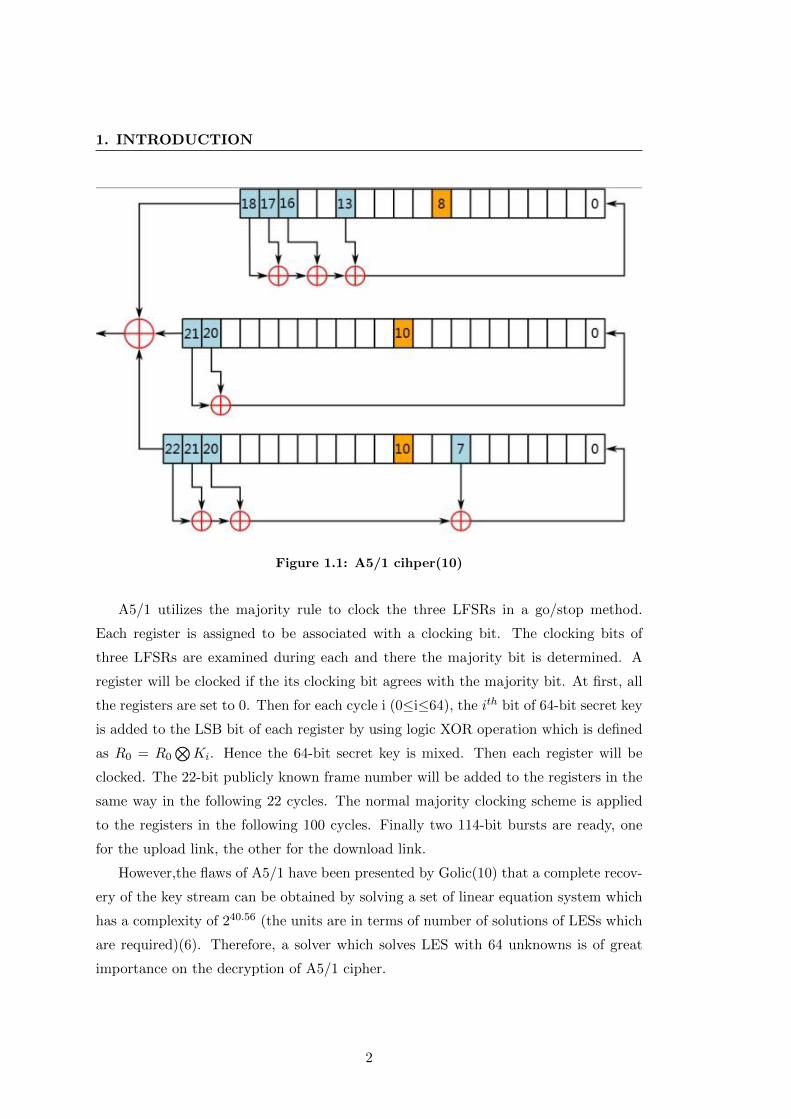
uses linear feedback shift registers (LFSRs) hardware implementation shown in Figure
1.1.The three LFSRs are specified in Table 1.1. The bits shown in Table 1.1 are indexed
with the least significant bit (LSB) as 0.
LFSR Length Character Clocking Tapped
number in bits polynomial bit bits
1 19 x18+x17+x16+x13+1 8 13,16,17,18
2 22 x21+x20+1 10 20,21
3 23 x22+x21+x20+x7+1 10 7,20,21,22
Table 1.1: The three LFSRs for A5/1(1)
1
1. INTRODUCTION
Figure 1.1: A5/1 cihper(10)
A5/1 utilizes the majority rule to clock the three LFSRs in a go/stop method.
Each register is assigned to be associated with a clocking bit. The clocking bits of
three LFSRs are examined during each and there the majority bit is determined. A
register will be clocked if the its clocking bit agrees with the majority bit. At first, all
the registers are set to 0. Then for each cycle i (0≤i≤64), the ith bit of 64-bit secret key
is added to the LSB bit of each register by using logic XOR operation which is defined
as R0 = R0⊗Ki. Hence the 64-bit secret key is mixed. Then each register will be
clocked. The 22-bit publicly known frame number will be added to the registers in the
same way in the following 22 cycles. The normal majority clocking scheme is applied
to the registers in the following 100 cycles. Finally two 114-bit bursts are ready, one
for the upload link, the other for the download link.
However,the flaws of A5/1 have been presented by Golic(10) that a complete recov-
ery of the key stream can be obtained by solving a set of linear equation system which
has a complexity of 240.56 (the units are in terms of number of solutions of LESs which
are required)(6). Therefore, a solver which solves LES with 64 unknowns is of great
importance on the decryption of A5/1 cipher.
2

The aim of the project is to design a linear equation solver that can solve linear
equation systems with n unknowns (n≤64) in Z2 to perform a live A5/1 attack.
3

1. INTRODUCTION
4
2
Working Principle of the Analog
Linear Equation Solver
2.1 Iterative Method
Solving LESs with the help of Gauss-Jordan elimination method is widely adopted for
the implementation of LES solvers such as GSMITH in (14). However, Gauss-Jordan
elimination has an asymptotic complexity of o(n3), which leads to an unsatisfying result
in some practical applications.
In (7), Benedikt Driessen presents the potential of implementing a kind of analog
LES solver. Unlike the common LES solvers, the proposed analog solver utilizes the
feedback network, which represents a corresponding LES, to settle down in a consid-
erably short time. In other words, the circuit is able to solve the LESs in constant
time and the stable operating points at the output of the circuit will represent the
solution set of the given LES. The feedback network also provides the solver with more
resistance to power attack.
The idea is based on the stationary Jacobi iterative method. Given a LES with n
unknowns:
A · −→x =−→b (2.1)
where A =
a11 a12 . . . a1na21 a22 . . . a2n...
.... . .
...an1 an2 . . . ann
, −→x =
x1x2...xn
,−→b =
b1b2...bn
5

2. WORKING PRINCIPLE OF THE ANALOG LINEAR EQUATIONSOLVER
Then A can be represented as the sum of a diagonal component D and the remainder
R.
A = D + R (2.2)
where D =
a11 0 . . . 00 a22 . . . 0...
.... . .
...0 0 . . . ann
, R =
0 a12 . . . a1na21 0 . . . a2n...
.... . .
...an1 an2 . . . 0
.
Therefore Equation 2.1 can be rewritten as:
(D + R) · −→x =−→b (2.3)
and at last:
D · −→x =−→b −R · −→x (2.4)
The Jacobi method calculates the left hand-side −→x by using previous −→x on the
right hand side with the following expression:
−→x (k+1) = D−1 · (−R · −→x (k) +−→b ), k ∈ N (2.5)
Starting with a given initial vector −→x (0) and repeating iteration, the sequence of
the approximations −→x will eventually converge to the actual solution in base-10 with
a very small error. The LESs can be solved by using the Jacobi method if Matrix A is
strictly or irreducibly diagonally dominant(2). Thus only the LESs in Z2 with Matrix
A, which has all 1 entries on the main diagonal, can be solved by Jacobi method in
base-10. Since the aim of the solver is to solve LESs over F2, additional conversion step
is needed to interpret the rational solution in base-2.
There is a very important fact related with the base-10 solution of a LES with 64
unknowns, which is that the values of the solution can even exceed 104 in some cases.
Thus, the actual solutions in base-10 can not be presented directly in the analog solver
and the internal module-2 reduction has to be applied in the design to solve the problem
.
Based on all said above, an analog solver is proposed in the following chapter.
6
2.2 Overview of the Analog Solver
2.2 Overview of the Analog Solver
The proposed linear equation solver is able to solve the linear equation systems of
following preconditions:
• A · −→x =−→b ,A ∈ Fn×n
2 ,−→x ,−→b ∈ Fn2
• All the diagonal entries of matrix A are 1.
• A · −→x =−→b is unique solvable in Z2,
The solver mainly consists of analog adder and folding ADC stage. A chain of
operational amplifiers forms the analog adder and performs arithmetic calculation to
get intermediate result s in base-10. Then the subsequent folding ADC stage performs
module-2 reduction to interpret the intermediate results in base-2. Output of the
folding ADC stage is then fed back into the analog adder through the feedback network
to repeat iterations. Finally when the circuit settles down, the output of the circuit
provides the base-2 solution.
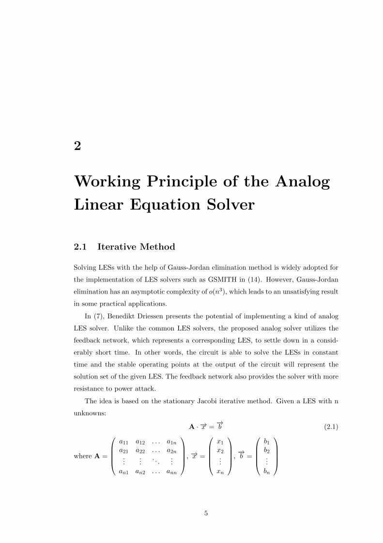
2.2.1 The Analog Adder
The operational amplifiers (op-amps) are used as the main building block of inverting
adders as shown in Figure 2.1 in the proposed topology.
The inverting adder in Figure 2.1 brings
Uout = −R4(U1
R1+U2
R2+U3
R3) (2.6)
If all the resistors are chosen equally, the Equation 2.6 can be simplified in the
following form:
Uout = −(U1 + U2 + U3) (2.7)
Based on this, a linear equation solver circuit with switch-based feedback network
can be constructed to perform the calculation to solve the linear equation systems:
A · −→u = −−→b · Uin (2.8)
where Uin is the input voltage.
7
2. WORKING PRINCIPLE OF THE ANALOG LINEAR EQUATIONSOLVER
+
_
R1
R2
R3
R4
U1
U3
U2
Uout
Figure 2.1: Inverting adder(7)
It can be seen that the solution of linear equation system is proportional to the
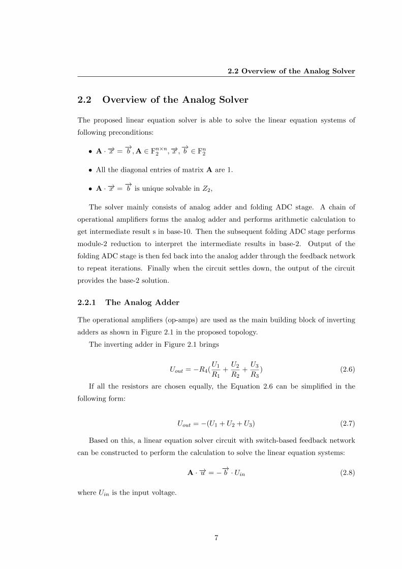
input voltage, which will be set to the basic analog level that represents 1 in base-10.
An example of the circuit for the case where n=3 is shown in Figure 2.2.
Depending on the coefficients of A and−→b , the switches are set to open or closed.
Equations for expected output voltages are:U1 = −b1 · Uin − a12 · U2 − a13 · U3
U2 = −b2 · Uin − a21 · U1 − a23 · U3
U3 = −b3 · Uin − a31 · U1 − a32 · U2
(2.9)
By rearranging the equations, a linear equation system is represented:
U1 + a12 · U2 + a13 · U3 = −b1 · Uin
U2 + a21 · U1 + a23 · U3 = −b2 · Uin
U3 + a31 · U1 + a32 · U2 = −b3 · Uin
(2.10)
Therefore the circuit computes the solutions of LESs with 3 unknowns and the
LESs are form of Equation 2.8. The LES shown in Equation 2.10 has a Matrix A
whose diagonal entries are all 1, so it fulfills the pre-condition of the Jacobi method.
8

2.2 Overview of the Analog Solver
+
_
+
_
+
_
R
R
R
R
R
R
R
R
R
R
R
R
-Uin
b1
b2
b3
a13
a12
a21
a32
a31
a32
U1
U2
U3
Figure 2.2: The basic schematic of the solver for 3 unknowns(7)9
2. WORKING PRINCIPLE OF THE ANALOG LINEAR EQUATIONSOLVER
2.2.2 The Folding ADC Stage
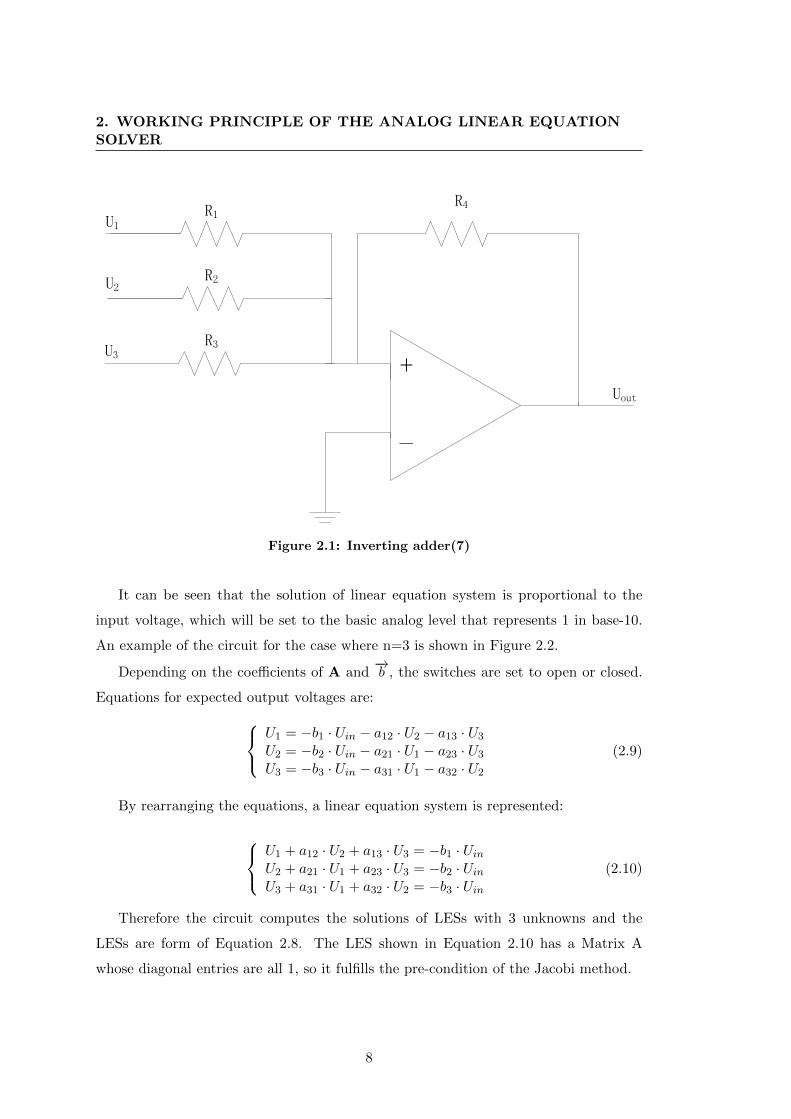
The folding technique is a type of analog processing that is widely used to reduce the
number of comparators used in a flash type ADC(9). The input signal is mapped or
folded into a sawtooth waveform, which is shown is Figure 2.3. The number of required
comparators is determined by the folding factor, which is 8 in the case of Figure 2.3.
Vin
Vout
Full flash
256 levels
Folding
32 levels
Figure 2.3: Transfer curve of folding circuit compared with the one using full
flash type(5)
Figure 2.4 shows the schematic of the CMOS folding circuit consisting of 4 NMOS
differential pairs with outputs odd-even crossed-coupled. One of the two inputs of
differential pairs is connected to the input voltage, and the other one is connected to the
reference voltage, which increases linearly. Actually, it is very difficult to generate the
sawtooth waveform shown in Figure 2.3, and the top and the bottom of the waveform
are rounded as shown in Figure 2.5. In practical application, additional CMOS folder
is added to generate a shifted folding signal to overcome the drawback (5). Since the
output in this design is in binary set 0,1, the rounded top and bottom do not affect
the performance of the circuit. This is the case that as long as the distance between
the two adjacent zero-crossings in the transfer curve, which indicates corresponding
10

2.2 Overview of the Analog Solver
reference voltages, can be approximately considered as constant.
Vdd
Vss
Vin Vin Vin VinVref1 Vref2 Vref3 Vref4
R R
Figure 2.4: CMOS folder
Figure 2.5: Transfer curve of the CMOS folder(11)
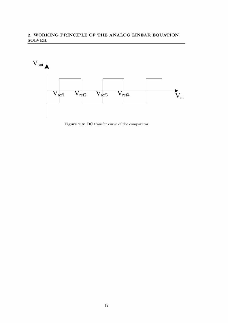
The differential outputs of the CMOS folder are connected to a comparator to
convert the folding signal to the binary signal shown in Figure 2.6. In Figure 2.6, the
output binary signal is 1 when the input is larger than 0, and vice versa.
11
2. WORKING PRINCIPLE OF THE ANALOG LINEAR EQUATIONSOLVER
Vout
VinVref1 Vref2 Vref3 Vref4
Figure 2.6: DC transfer curve of the comparator
12
3
Hardware Implementation of the
Analog Solver
3.1 The Analog Adder
3.1.1 The Specification of the Operational Amplifier
After introducing the internal module-2 reduction in the design, the possible value
in base-10 obtained at the output of the analog adder is in the range of -63 to 1 in
the practical applications with 64 unknowns. Considering the output range, the low-
threshold voltage CMOS transistors in 0.18µm standard CMOS technology with the
supply voltage of 3.3V are chosen to implement the hardware. It is important to note
that the analog voltage level that represents value oen in base-10 is 20 mV in the
design, and this means that less than 1% in the resistor matching is required during
the fabrication. The minimum DC gain of 80 dB is required to control the gain error
within 5% while the op-amp is operated for the applications with 64 unknowns. The
basic specification of the operational amplifier is listed in Table 3.1.
3.1.2 The Implementation of the Analog Adder
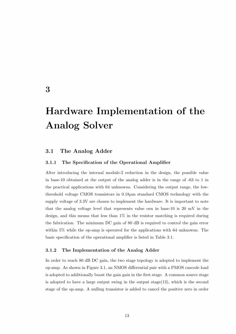
In order to reach 80 dB DC gain, the two stage topology is adopted to implement the
op-amp. As shown in Figure 3.1, an NMOS differential pair with a PMOS cascode load
is adopted to additionally boost the gain gain in the first stage. A common source stage
is adopted to have a large output swing in the output stage(13), which is the second
stage of the op-amp. A nulling transistor is added to cancel the positive zero in order
13

3. HARDWARE IMPLEMENTATION OF THE ANALOG SOLVER
Supply Voltage: Vdd +1.65V
Supply Voltage:Vss -1.65V
Load Capacitance: CL 5pF
DC gain: A0 ≥80 dB
Slew Rate: SR 10V/µsec
Output Swing:V(max,min)out ±1.28V
Phase Margin:ΦM ≥ 45
Table 3.1: Op-amp basic specification
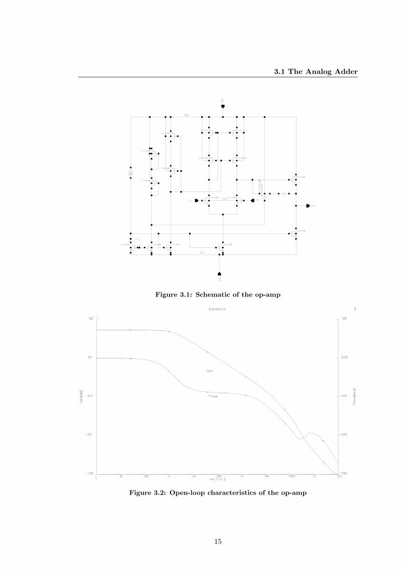
to enlarge the unity gain bandwidth (4). The op-amp achieves a DC gain of 86 dB with
a GB of 30.07 MHz, which is shown in the Figure 3.2. Meanwhile the phase margin of
50 makes the op-amp function correctly when the op-amp is working in closed loop.
All the simulation results are shown in Table 3.2.
By appropriately connecting the op-amps with resistors and switches, the feedback
network of the analog adder is constructed. An example of 3-input analog adder is
shown in Figure 3.3.
A0 86 dB
ΦM 50
Vmaxout 1.335V
Vminout -1.373V
Input Common Range: V+CMR 1.362V
V−CMR -1.638V
Common Mode Rejection Ratio: CMRR 124.778dB
Power Supply Rejection Ratio: PSRR+ 130.786dB
PSRR− 133.416dB
SR+ 100.124V/µsec
SR− -27.626V/µsec
Table 3.2: Simulation results of the op-amp
14
3.1 The Analog Adder
Figure 3.1: Schematic of the op-amp
Figure 3.2: Open-loop characteristics of the op-amp
15

3. HARDWARE IMPLEMENTATION OF THE ANALOG SOLVER
Figure 3.3: 3-input analog adder
16

3.2 The Folding ADC
3.2 The Folding ADC
In order to reduce the required number of comparators used in the solver with 64
unknowns, a CMOS folder with a folding factor of 16 is chosen as shown in Figure
3.4. Therefore, in the design only 4 comparators are needed to perform the module-2
reduction. Considering the input common range of the CMOS folder and the output
of the analog adder, the 16 reference voltages linearly increases from -1.2V to 1.2V,
and the difference between the adjacent two reference voltages is 160 mV. The resistors
used in Figure 2.4 are replaced with PMOS load because the value of the resistance is
not accurate in CMOS process(12).
Figure 3.4: 16-stage CMOS folder
Due to the unbalanced DC current flowing in the two output nodes, there is no
intersection for the two output waveforms, as shown in Figure 3.5. Thus, in order
to balance the current, an additional current mirror is added to the folder so that
two output waveform are shifted and they intersects at the correct points of reference
voltages, which is shown in Figure 3.6.
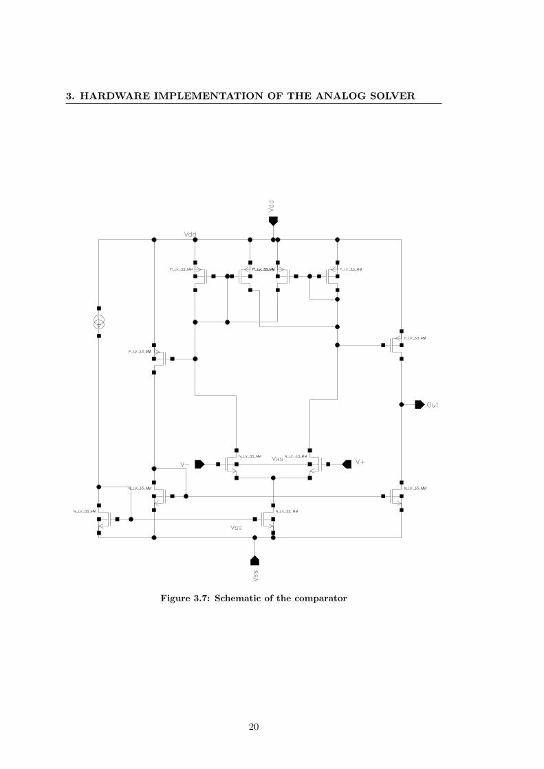
See Figure 3.7 for the schematic of the comparator used in the design. The proposed
has a input resolution of 5 mV. The positive feedback employed in the PMOS load in
17

3. HARDWARE IMPLEMENTATION OF THE ANALOG SOLVER
Figure 3.5: Output waveform of the folder without a current mirror
Figure 3.6: Output waveform of the folder with a current mirror
18

3.2 The Folding ADC
the first stage of the comparator has two main functions. Firstly it can achieve a high
output resistance. Secondly it provides the comparator with the internal hysteresis to
make the comparator have a certain tolerance towards environmental noise(4). The
ratio of the sizes of corresponding transistors in the PMOS load determines the degree
of the hysteresis.
The simulation waveform of the folding ADC is shown in Figure 3.8. Comparing the
16 zero-crossings shown in the simulation waveform with the setting reference voltages,
the relative errors are quite small, the maximum of which is 3.125%. All of the relative
errors are smaller than threshold error, which is 6.25 % (1/16) in this case. See Table
3.3 for the corresponding data.
No. Simulation Expected Relative
results(V) reference voltage (V) error
1 -1.187 -1.2 1.08%
2 -1.048 -1.04 0.77%
3 -0.8725 -0.88 0.85%
4 -0.7275 -0.72 1.04%
5 -0.5525 -0.56 1.34%
6 -0.4025 -0.4 0.63%
7 -0.2375 -0.24 1.04%
8 -0.0825 -0.08 3.13%
9 0.0825 0.08 3.13%
10 0.2375 0.24 1.04%
11 0.4025 0.4 0.63%
12 0.5575 0.56 0.45%
13 0.7225 0.72 0.35%
14 0.8775 0.88 0.28%
15 1.043 1.04 0.29%
16 1.197 1.2 0.25%
Table 3.3: Comparison between zero-crossings in the output waveforms and reference
voltages
19
3. HARDWARE IMPLEMENTATION OF THE ANALOG SOLVER
Figure 3.7: Schematic of the comparator
20

3.3 Level Shifter
Figure 3.8: DC sweep simulation result of the folding ADC
3.3 Level Shifter
As mentioned above, the analog adder and folding ADC are working together in the
feedback network, but they cannot be directly installed together because the input range
and output range of the two are not compatible with each other. Additional Block is
needed to perform level shifting in order to make both of them function correctly.
The output of the analog adder varies from -1.26V to 0.02V, which stands for from
-63 to 1 in base-10. There is a difference of 20 mV between each analog level. However,
as stated above, the folding stage can only handle the 16 analog levels with a difference
of 160 mV, from -7 to 8 in base-10. Therefore, the level shifter, shown in Figure 3.9, is
designed to connect the output of analog adder to the folding ADC, and it consists of
two stages: the decision stage, the shifting stage.
The decision stage observes the output of the analog adder, and then allocates it
into the following listed regions depending on the value it represents in base-10: -7 to
1, -23 to 8, -39 to 24, -55 to 40, and -63 to 56. Four comparators with their respective
reference voltages (-1.11V, -790mV, -470mV, - 150mV) determine in which region the
21

3. HARDWARE IMPLEMENTATION OF THE ANALOG SOLVER
output is and generate the corresponding logic signals, 1.65V for true, and -1.65V for
false.
A shifting stage block consists of an operational amplifier, 4 CMOS switches and
12 resistors to perform addition and multiplication. There are eight resistors in the
feedback path, and all the resistors should have the same value of resistance, which in
1 MΩ in the design. The logical signals generated by the decision stage determine the
status of CMOS switches. The output voltage is expressed as follows:
Vout = −8(Vin + 320×N)(mV ) (3.1)
where N indicates the number of closed CMOS switches.
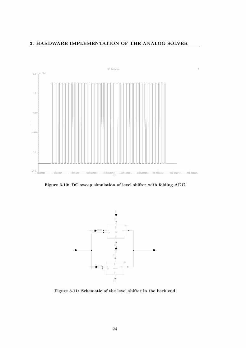
According the DC sweep simulation results shown in Figure 3.10, the folding ADC
stage functions correctly with the proposed level shifter when the input signal varies
from -1.5 V to 0.05 V, and that covers the output range of analog adder.
As for the level shifter for connecting the folding ADC to the analog adder, it be-
comes much simpler since there are only two levels at both the input and the output.
A multiplexer shown in Figure 3.11 can perform such level shifting. The signal control-
ling two switches comes from the output of the folding ADC stage. When the signal is
high, the upper switch is turned on and the lower one is turned off. Then the output
is analog level 1 (20 mV). On the contrary, when the signal is low, the upper switch is
open, and the lower one is closed. Therefore, the output is analog level 0 (0 mV).
3.4 Top-level Schematic
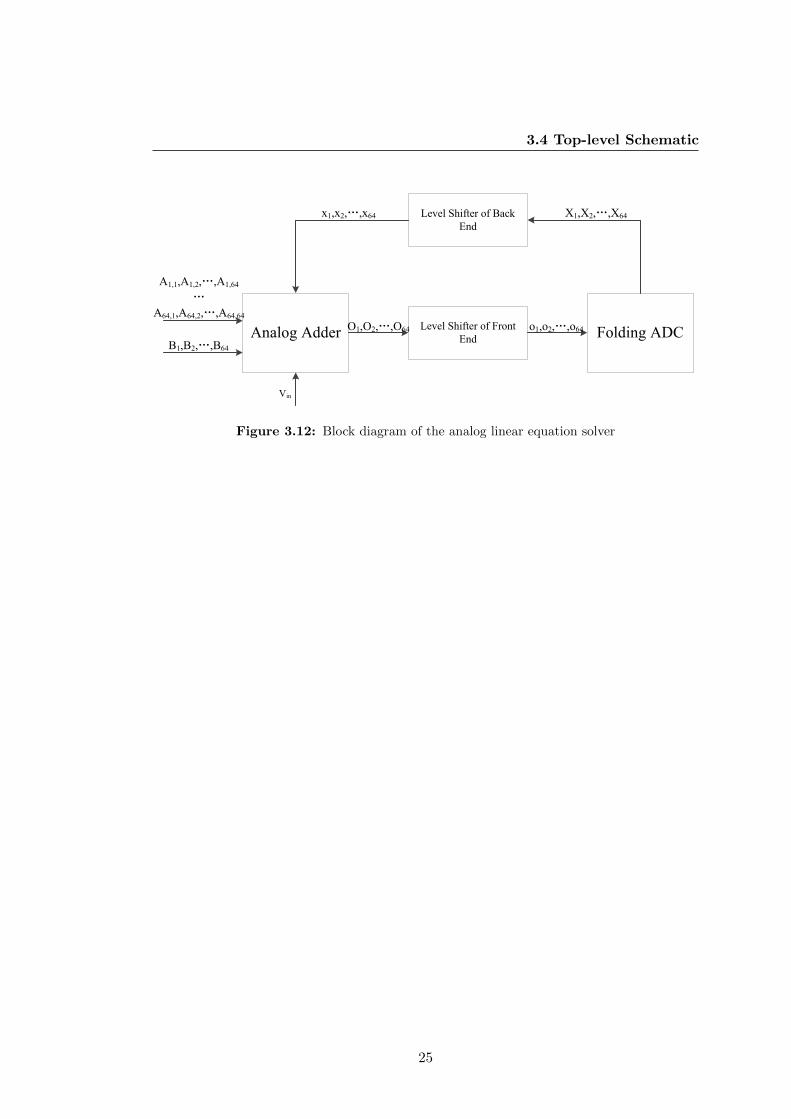
See the complete block diagram of the analog solver shown in Figure 3.12 for the
connection of the components. The coefficients of Matrix A and−→b set the status of
the switches in the feedback network, and the solution is obtained at the output of the
folding ADC stage.
22

3.4 Top-level Schematic
Decesion stage Shifting Stage
Figure 3.9: Schematic of level shifter at the front end
23
3. HARDWARE IMPLEMENTATION OF THE ANALOG SOLVER
Figure 3.10: DC sweep simulation of level shifter with folding ADC
Figure 3.11: Schematic of the level shifter in the back end
24
3.4 Top-level Schematic
Analog Adder Folding ADC
Level Shifter of Back
End
Level Shifter of Front
End
O1,O2,…,O64 o1,o2,…,o64
X1,X2,…,X64x1,x2,…,x64
A1,1,A1,2,…,A1,64
…
A64,1,A64,2,…,A64,64
B1,B2,…,B64
Vin
Figure 3.12: Block diagram of the analog linear equation solver
25

3. HARDWARE IMPLEMENTATION OF THE ANALOG SOLVER
26

4
Test of the analog solver
4.1 Test with 4 Unknowns
We start the test of the analog linear equation solver with a simple case, the linear
equation systems with 4 unknowns. In order to reduce the complexity and the simula-
tion time, the unnecessary part in the test for LESs with 4 unknowns, such as the level
shifter in the front end, is removed from the solver. The analog level 1 is adjusted to
300 mV. Hence, the difference between reference voltages in the CMOS folder is also
set to 300 mV. All the input A matrices that result in an unique solution are generated
by Matlab code shown in Appendix A. All of them together with random−→b vectors
are written into corresponding files. Cadence spectre program reads the stimuli from
the files and then set the status of CMOS switches in the feedback network to represent
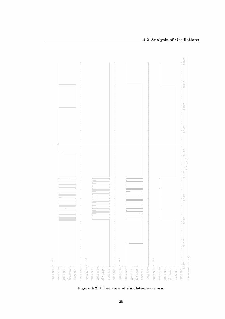
the give LESs. Simulation results are shown in Figure 4.1 and 4.2.
4.2 Analysis of Oscillations
The simulation results show that about the solver does work in about 20% cases but fails
in rest cases. Analyzing the simulation results, an interesting phenomena is observed.
Oscillations are always observed at the output when it fails to find the correct solution
of LESs. When the circuit does not oscillate, the solver gets the correct solution of the
given LES. This phenomenon conforms the fact that oscillation links with the wrong
solution, and the correct solution is the stable operating point of the circuit.
27

4. TEST OF THE ANALOG SOLVER
Figure 4.1: Transient simulation of some input test vectors
28
4.2 Analysis of Oscillations
Figure 4.2: Close view of simulationwaveform
29

4. TEST OF THE ANALOG SOLVER
4.2.1 The Source of the Oscillation
A quite common reason that causes oscillations in the chain of op-amps is the positive
feedback in the loop. Therefore, it is necessary to break the feedback loop. Inserting
either capacitors or Flip-flops(FFs) in the feedback loop can achieve this. The Flip-flop
is preferred in the design due to its predictable behavior. To reduce the complexity of
clock scheme and number of FFs, the D-type FFs (DFFs) shown in Figure 4.3 are in-
serted at the outputs of the analog adders, and all the DFFs are clocked simultaneously.
Figure 4.3: Schematic of the DFF
In opposition to what is expected, the simulation shows the situation is much worse
than that without DFFs. Among 1688 input cases, only several of them can get the
correct solutions, and the rest of them completely cause oscillations. Therefore, the
possibility that the positive feedback causes oscillation can be excluded.
The proposed solver gets the solution by using iteration method, which is realized by
the feedback network in the design. After reviewing the oscillations, it can be observed
that the oscillations consist of a repeated sequence of −→x vectors instead of a random
sequence. One of the examples is shown in Figure 4.4. Analyzing the −→x vectors in the
repeated sequence, we can draw the conclusion that that the process of iterations is the
30
4.2 Analysis of Oscillations
right source to cause the oscillations.
In the design, the solver is set to start with the initial−→x (0) vector with all coefficients
0, and calculates the new −→x (1) vectors with associated A matrix and−→b vector. Then
the solver continues to calculate −→x (k+1) by using −→x (k+1) until −→x (k+1) equals −→x (k), and
−→x (k+1) is the solution of the calculated linear equation system. The element-based
formula can be presented as follows:
x(k+1)i = bi −
∑j 6=i
a(i,j) · x(k)j , k ∈ N, i, j ∈ N&i, j ≤ 64, x
(0)i = 0 (4.1)
The Jacobi iterative method works in solving LESs in base-10, but it makes difference
when using the method together with internal module-2 reduction to solve LESs in
base-2. Using the method may generate a sequence of −→x vectors which finally do not
lead to convergence in most cases in base-2, and the repeated sequences analyzed by
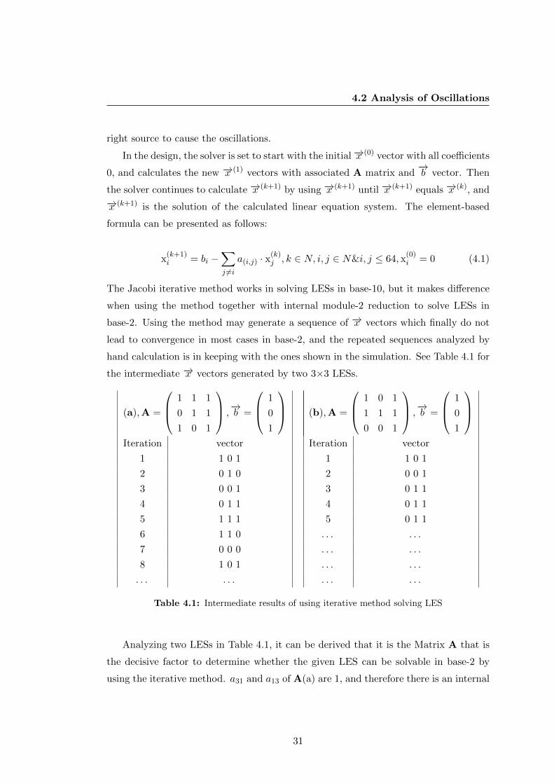
hand calculation is in keeping with the ones shown in the simulation. See Table 4.1 for
the intermediate −→x vectors generated by two 3×3 LESs.
(a),A =
1 1 1
0 1 1
1 0 1
,−→b =
1
0
1
(b),A =
1 0 1
1 1 1
0 0 1
,−→b =
1
0
1
Iteration vector Iteration vector
1 1 0 1 1 1 0 1
2 0 1 0 2 0 0 1
3 0 0 1 3 0 1 1
4 0 1 1 4 0 1 1
5 1 1 1 5 0 1 1
6 1 1 0 . . . . . .
7 0 0 0 . . . . . .
8 1 0 1 . . . . . .
. . . . . . . . . . . .
Table 4.1: Intermediate results of using iterative method solving LES
Analyzing two LESs in Table 4.1, it can be derived that it is the Matrix A that is
the decisive factor to determine whether the given LES can be solvable in base-2 by
using the iterative method. a31 and a13 of A(a) are 1, and therefore there is an internal
31

4. TEST OF THE ANALOG SOLVER
Figure 4.4: The Repeated Sequence in the Oscillations
32
4.2 Analysis of Oscillations
loop caused by Equation 1 and Equation 3 of the LES(a). The value of x1 is determined
by x3 according to Equation 4.1, and vice versa. Therefore, the values of x1 and x3 in
the solution set of LES(a) are most likely to switch between 0 and 1 during iterations
due to two-value target set of 0, 1, and thus the solver cannot find the stable point
of the circuit. However, there is no such loop in Matrix A(b) and therefore the solver
becomes stable after trying some times of iterations.
4.2.2 Prevention of Oscillations
To prevent the oscillations in the solver, a way to deal with internal loops in Matrix
A is needed to be developed. Spotting the loops and breaking the loops can solve the
problem. However, it will need a pre-processing block and the important thing is that
the corresponding block is not area efficient. In addition, the algorithm that can handle
the spotting and breaking the loops is of exponential complexity.
Burak Erbagci proposed a kind of clocking scheme for DFFs to prevent oscillation for
the LES solver which is complemented in the digital domain(8). The DFFs are allocated
with different clock signals according to Matrix A and the method has been verified
that it works for the LESs with 4 unknowns and works at least for the tested LESs
with 8 unknowns1. However, the same problem remains that the algorithm is inefficient
and an additional pre-processing circuit is needed, which introduces additional costs
in terms of silicon area, power consumption and latency according to the proposed
clocking scheme.
However, the proposed clocking time express the idea that the oscillations could be
prevented by introducing internal loops at appropriate time so that the element-based
formula of iterations shown in Equation 4.1 is changed and therefore the sequence of −→xis also changed. Based on this idea, a self-adjusted circuit shown in Figure 4.5 is added
to perform clock allocation to introduce loops. The circuit is composed by a logic XOR
gate and a multiplexer. The circuit samples same ith bit of two consecutive calculated
intermediate results and compares them. The corresponding bit DFF will be clocked
with a signal of a smaller period if the results are the same, otherwise the DFF will
be clocked with a signal of a larger period. The difference means there are oscillations
reported at the corresponding feedback path and then the feedback loop is set to be
1Complete test is not done and the validity of the clocking scheme is not justified
33

4. TEST OF THE ANALOG SOLVER
disconnected for a while. By doing this that feedback loops are broken according to
the intermediate results.
Figure 4.5: Schematic of the self-adjusted circuit
The simulation shows that it works fine for all the LESs with 4 unknowns as shown
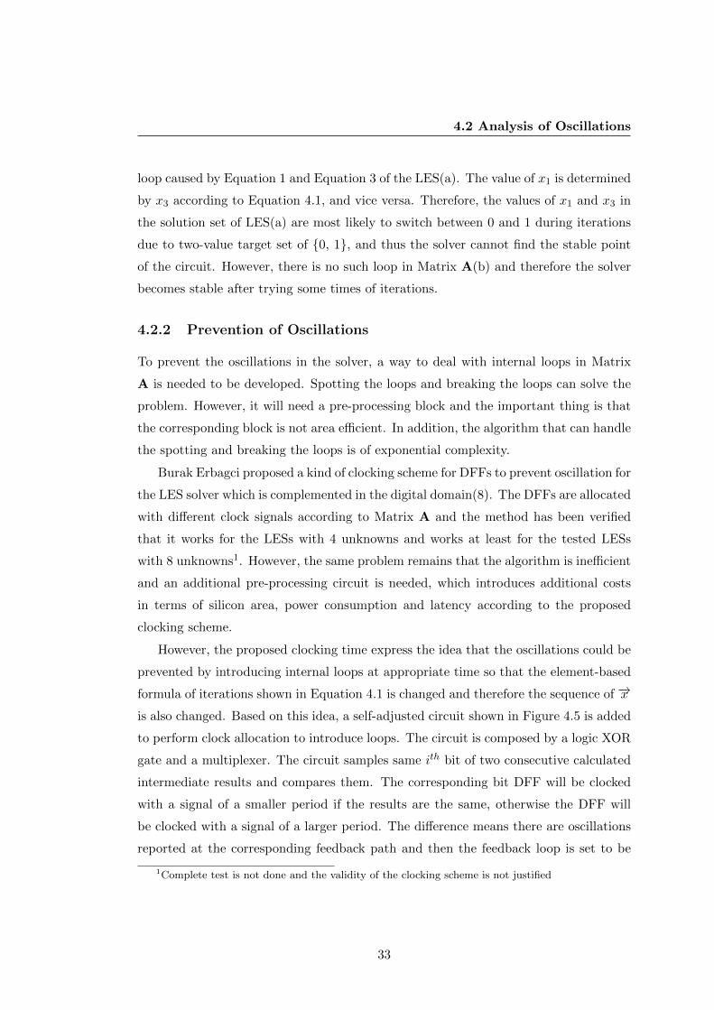
in Figure 4.6 and Figure 4.7. Note that the time set for calculation is 20 us, and 10
us for reset vectors to all 0. However, when the LES extends with 8 unknowns, the
method fails with some cases.
Figure 4.6: Simulation for LESs with 4 unknowns with the proposed clocking scheme
34
4.2 Analysis of Oscillations
Figure 4.7: Close view of the waveform
35

4. TEST OF THE ANALOG SOLVER
36

5
Solving the Problem in Digital
Approach
After trying the methods above, it becomes clear that prevention of the oscillation relies
on how the internal loops in the Matrix A are introduced into the solver. The way
to introduce the loops determines the results of iterations. Therefore, a pre-processing
circuit that deals with Matrix A of LES is necessary in the design. However, the pre-
processing circuit has to be absolutely implemented in the digital domain. As a result,
the LES solver implemented in the digital approach in [6] is introduced.
5.1 The Implementation of the Digital Solver
A LES with 3 unknowns in the following form:x1 + a12 · x2 + a13 · x3 = b1x2 + a21 · x1 + a23 · x3 = b2x3 + a31 · x1 + a32 · x2 = b3
(5.1)
can be rewritten as follow:x1 = b1 + a12 · x2 + a13 · x3x2 = b2 + a21 · x1 + a23 · x3x3 = b3 + a31 · x1 + a32 · x2
(5.2)
After replacing addition with XOR and multiplication with and, it becomes:x1 = b1
⊗(a12
⊕x2)
⊗(a13
⊕x3)
x2 = b2⊗
(a21⊕x1)
⊗(a23
⊕x3)
x3 = b3⊗
(a31⊕x1)
⊗(a32
⊕x2)
(5.3)
37

5. SOLVING THE PROBLEM IN DIGITAL APPROACH
The schematic of LES solver which solves the form of Equation 5.3 is shown in
Figure 5.1.
As seen in Figure 5.1, in order to avoid the potential oscillation caused by the
combinational behavior of the circuit, DFFs are inserted at the output of the XOR
gates, which provide the solutions. All the DFFs are clocked simultaneously to reduce
the clocking complexity. The implemented digital confronts with the same oscillation
issue as observed in the analog solver as shown in (8).
5.2 The Pre-processing Circuit
As stated before, the solver needs a pre-processing block to deal with the LES, so
that the solver is able not to oscillate and function correctly. The complexity of the
algorithm the pre-processing block utilizes is also an important factor to be considered.
The function of the pre-processing circuit is discussed below.
5.2.1 Random Initial Vector
Until now, the solver is supposed to start to calculate the LES with the initial −→x (0)
vector of all 0 coefficients, and the initial −→x (0) vector will absolutely affect the sequence
of intermediate initial −→x vectors. The intermediate nitial −→x vectors has a direct impact
on the final result of iterations. Therefore, firstly the pre-processing circuit is thought
to generate random initial vector and then the vector is fed into the solver. The solver
starts to calculate LES with a given −→x (0) vector. Then the pre-processing circuit will
wait for the solver to settle down. If the solver still oscillates in a certain time, the
pre-processing circuit will generate another−→x (0) vector and then solver starts another
calculation with this one. Finally, the solver will certainly come to a stable status,as
long as it finds the correct solution.
It can be convinced that at least one initial −→x (0) vector can make the solver stable,
and that initial −→x (0) vector is the correct solution of the given LES. In order to verify
the efficiency of the method, it should be checked how many other initial −→x (0) vectors
outside the solution set can make the solver stable.
The solver with 8 unknowns is chosen to verify the method in order to have a good
balance between effectiveness and simulation time. Fifty different matrices A with all
possible 256 (28 =256) −→x (0) vectors are fed into the solver.
38

5.2 The Pre-processing Circuit
x2
a12
a13
x3
b1
X1
a21
x1
a23
x3
b2
X2
a31
x1
x2
a32
b3
X3
SET
CLR
D
CK
Reset
SET
CLR
D
CK
Reset
SET
CLR
D
CK
Reset
Figure 5.1: Schematic of digital LES solver with 3 unknowns
39
5. SOLVING THE PROBLEM IN DIGITAL APPROACH
The result is very disappointed. The solver is able to be stable with only 2-4 out
of 256 −→x (0) vectors on average for most of Matrices A. Moreover, in some cases, the
solver reaches to the stable status with only one −→x (0) vectors, which is exactly the
solution we want. Therefore the algorithm has a complexity of o(2(N−1)) and that is
too inefficient. Thus the algorithm has to be abandoned.
5.2.2 Spanning Tree
According to the definition of the spanning tree, the spanning tree of Matrix A is a
matrix without internal loops. The solver will not oscillate with the spanning tree of
Matrix A. Thus, a new algorithm is defined as follows:
• Compute the spanning tree of the Matrix A: A0.
• Compute L = L−A0. L contains all the possible internal loops of the Matrix A.
• Distribute all the 1s of L to as many matrices as possible, L1, L2, etc., such that
L = L1 + L2 + Lm. Each Li contains one internal loop of Matrix A.
• A1 = A0 + L1, A2 = A1 + L2,,and finally Am = Am−1 + Lm. Am is equal to
the original Matrix A. Each Ai has one more internal loop than Ai−1.
The solver will start with A0, and then A1,.., and finally with Am(A). The algo-
rithm is meant to introduce only one more internal loop for each step of calculation with
a new Matrix Ai, and the spanning tree algorithm has a lower complexity of o(N2).
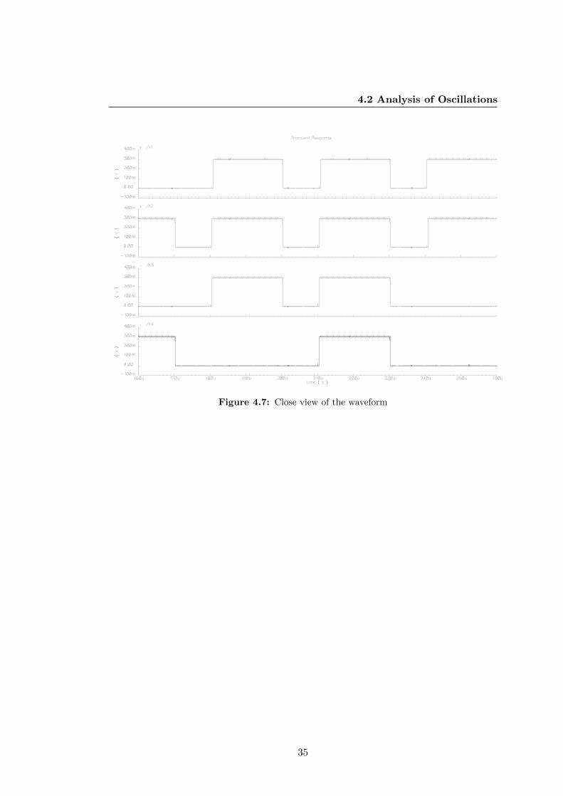
The simulation is also done with the solver designed for 8 unknowns. However, the
new algorithm still turns out to be incorrect. The solver still oscillates in most of cases
as shown in Figure 5.2.
Figure 5.2: Simulation results with spanning tree algorithm
40

5.2 The Pre-processing Circuit
5.2.3 Gaussian Elimination
All the algorithms tested above tell the truth that the solver can and only can have the
correct solution when the Matrix A do not have any internal loops, no matter what
the initial −→x (0) vector is. In other words, the proposed solver implementation can only
deal with the LES when there are no internal loops within the Matrix A. Of all forms
of Matrix, the unitriangular matrix is rightly a form of matrix which do not have any
internal loops and the simulation results show the same conclusion. The solver becomes
stable with the unitriangular matrix of n up to 64.
The problem arises from how we get an equivalent LES with an unitriangular Matrix
A from an original LES. The equivalent LES should have exactly same solution set as
the original LES. Gaussian Elimination is a good choice to solve the problem. By using
Gaussian Elimination, an equivalent LES composed of an upper-triangular Matrix A
and corresponding−→b vector can be realized. Then the implemented solver can be used
to perform backward substitution to get the correct solution with the equivalent LES.
The proposed algorithm has a complexity, which is nearly half of Gauss-Jordan
elimination. Gauss-Jordan elimination reduce the matrix to the reduced row echelon
form, and has a asymptotic complexity of N3.
The simulation also shows that the solver will finally become stable and get the
correct solution with the equivalent, while solving the LES with n up to 64.
5.2.4 LU Decomposition
LU decomposition or LU factorization, is a matrix decomposition which represents the
matrix as a product of a lower triangular matrix and an upper triangular matrix(3),
and the triangular matrix do not have any internal loops. So the LU decomposition
can also be applied as the algorithm used in the pre-blocking block. However, using
LU decomposition to solve LESs has some differences compared with the one using
Gaussian Elimination.
Give a LES A · −→x =−→b , it can be rewritten by using LU decomposition as:
L ·U · −→x =−→b (5.4)
where L is a lower triangular matrix, U is a upper triangular matrix.
Then the solution can be in two step
41

5. SOLVING THE PROBLEM IN DIGITAL APPROACH
• Firstly, we solve the equation L · −→y =−→b for −→y .
• Secondly, we solve the equation U · −→x = −→y for −→x .
As long as the LU composition of the a given matrix A is given, the solution of the
corresponding LESs with random−→b can be solved, and it is faster than using Gaussian
Elimination to reduce the LESs. However, we need to use Gaussian Elimination or
equivalent to perform LU decomposition.
5.3 Implementation of the Complete LES Solver In Digi-
tal Approach
5.3.1 Working Principle
Finally, the proposed complete LES solver consists of a pre-processing circuit, a back-
ward substitution solver, and an oscillation detector. The block diagram is shown in
Figure 5.3.
The Gaussian Elimination algorithm used in the pre-blocking block is shown in
Table 5.1.
Pre-processing block
Backward Substitution
Solver
Oscillation Detector
A1,b1
X1
D_E
X
Figure 5.3: The block diagram of LES solver
42

5.3 Implementation of the Complete LES Solver In Digital Approach
Gauss Elimination over F2
Input: A ∈ Fn×n2 ,−→x , ai,i = 1,
−→b ∈ Fn
2
1:for each row l = 1 : n do
2: s← l
3: while as,l = 0 do
4: s← s + 1
5: end while
6: exchange −→as with −→al and bs with bl
7: for each row i = l+ 1 : n do
8: if ai,l 6= 0 then
9: bi = bi⊗bl
10: for each element j = l+ l : n do
11: ai,j = ai,j⊗al,j
12: end for
13: end if
14: end for
15: end for
Table 5.1: Gauss Elimination over F2
A given LES is fed into the pre-processing block and the backward substitution
solver simultaneously. Then the backward substation solver will try to solve the LES
for the first time while the pre-processing block performs Gaussian Elimination to
reduce the given LES.
The solver will not oscillate if the Matrix A of the LES has no internal loops. There-
fore, the solver becomes stable and then no oscillations are observed by the oscillation
detector.
In most cases, there are some internal loops within the Matrix A. Thus, the solver
will oscillate continuously, and the oscillation detector will keeping reporting oscilla-
tions detected when the pre-processing block finishes Gaussian Elimination. Then the
backward solver receives a new LES and performs backward substitution. The solver
should become stable at this time.
The LES solver outputs the correct solution of a given LES only when there is no
43
5. SOLVING THE PROBLEM IN DIGITAL APPROACH
oscillation detected at the output of the backward substitution solver.
5.3.2 Simulation Results
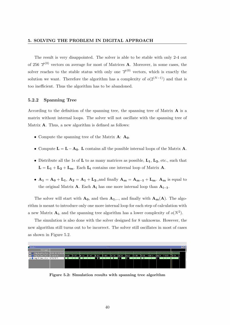
The simulation is done with the complete LES solver with 64 unknowns. 1427 LESs
with random Matrix A and−→b vector generated by Matlab are fed into the LES solver.
The solver works perfectly with all the input testing LES as shown in Figure 5.4.
All of them get the correct solutions, and no errors occur. According to the simulation
results, it takes the solver block 2236.4 clock cycles on average to perform Gaussian
Elimination, 32.06 clock cycles for backward substitution, 2261.4 to observe the solution
at the output.
.............................................................................................................................................................................................................................................................................................................................................
.............................................................................................................................................................................................................................................................................................................................................
.............................................................................................................................................................................................................................................................................................................................................
.............................................................................................................................................................................................................................................................................................................................................
0 ns+10 200000 ns 400000 ns
/ge_solver_top_test/t_a_in .............................................................................................................................................................................................................................................................................................................................................
/ge_solver_top_test/t_b_in .............................................................................................................................................................................................................................................................................................................................................
/ge_solver_top_test/t_done
/ge_solver_top_test/t_x_out .............................................................................................................................................................................................................................................................................................................................................
/ge_solver_top_test/true_x_out .............................................................................................................................................................................................................................................................................................................................................
Entity:ge_solver_top_test Architecture:testbench Date: Wed Aug 17 06:31:42 PM CEST 2011 Row: 1 Page: 1
Figure 5.4: Simulation results of top solver with 64 unknowns
5.4 Implementation of LU Decomposition
As for the LU decomposition, the implementation is similar. The only difference that
LU implementation needs two single backward substitution LES solvers instead. But
this two solvers do not need to have full feedback network, and only the half is enough
for the backward substitution.
Actually in the implementation, LUP decomposition, which is a variant of LU
decomposition, is adopted in order to ensure the L and U have all entries 1 on their
respective main diagonal. Therefore, What is different as stated above, the−→b vector
is also needed in the implementation of LUP algorithm.
The LUP decomposition algorithm is shown in Table 5.2.
As the algorithm shows, it is more complicated than previous Gaussian Elimination
algorithm.
Then LUP decomposition has been finished in VHDL coding and the simulation
shows it works.
44
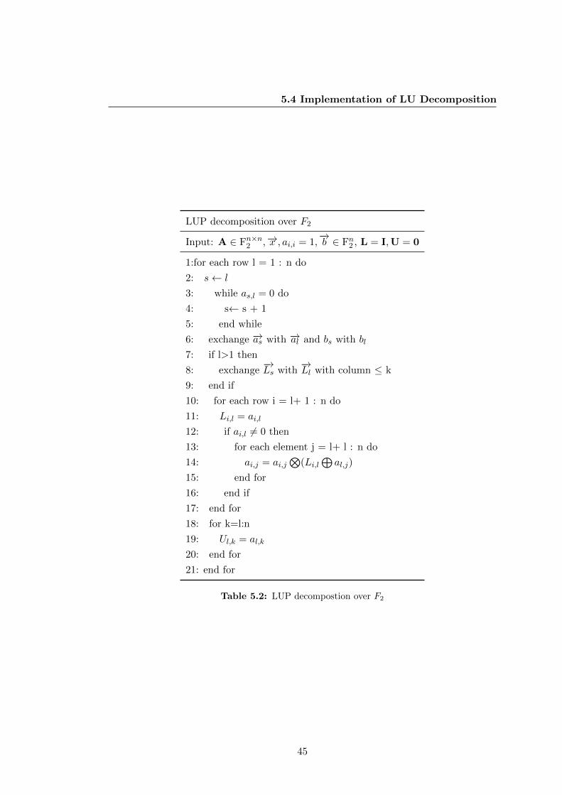
5.4 Implementation of LU Decomposition
LUP decomposition over F2
Input: A ∈ Fn×n2 ,−→x , ai,i = 1,
−→b ∈ Fn
2 , L = I,U = 0
1:for each row l = 1 : n do
2: s← l
3: while as,l = 0 do
4: s← s + 1
5: end while
6: exchange −→as with −→al and bs with bl
7: if l>1 then
8: exchange−→Ls with
−→Ll with column ≤ k
9: end if
10: for each row i = l+ 1 : n do
11: Li,l = ai,l
12: if ai,l 6= 0 then
13: for each element j = l+ l : n do
14: ai,j = ai,j⊗
(Li,l⊕al,j)
15: end for
16: end if
17: end for
18: for k=l:n
19: Ul,k = al,k
20: end for
21: end for
Table 5.2: LUP decompostion over F2
45

5. SOLVING THE PROBLEM IN DIGITAL APPROACH
46
6
Conclusions and Future work
6.1 Conlusions
The master project targeted to develop an analog solver. The proposed topology of the
analog solver should also handle the equivalent LES with upper-triangular Matrix A
theoretically, and can be integrated with the pre-processing block.
However, the analog solver has many disadvantages compared with the digital one.
Firstly, the analog solver has a limited choice of the technology. The supply voltage is
limited by the large output range. High supply voltage has a close relation with older
technology, and thus the solver has lower speed, lower integration density. Secondly,
the analog solver costs a lot of silicon area. The complexity of the solver, the high gain
of the op-amp, the moderate resistors, etc., all of them result in a large area of the
circuit. Then, the performance of the analog solver deeply relies on the accuracy of the
CMOS process. The analog level of op-amp can be easily affected by the input offset
voltage, matching level of the corresponding resistor blocks, and those factors are very
difficult to improve during the fabrication. Finally, as said before, in order to function
correctly, the solver needs to be integrated with a pre-preprocessing block, which has
to be implemented in digital domain. Thus auxiliary A/D converters and level shifters
are required.
In summary, a digital LES is a better choice considering the proposed implementa-
tion. The single digital solver can only deal with the LES whose Matrix A do not have
any internal loops. It needs a pre-processing block to extend its application field. The
proposed pre-processing block in the design performs Gaussian Elimination to reduce
47

6. CONCLUSIONS AND FUTURE WORK
given LES to an equivalent LES whose Matrix A is form of upper-triangular Matrix.
Auxiliary oscillation detector is used to observe the status of the backward substitution
and control the output of the complete LES solver. The correct function of the complete
LES solver has been verified by VHDL logic simulation, and the solver makes use of an
algorithm whose complexity is the half of GaussJordan elimination, and Gauss-Jordan
elimination is widely used in the current LES solver design.
6.2 Future work
Regarding the analog solver, the proposed topology using internal module-2 reduction
presents a few advantages. A new topology should be developed to cancel out the
drawbacks brought by the analog design. Since there are large-value immediate results
calculated in Base-10 by iteration, a key point in the design is how to reduce the
immediate results within a reasonable range. The results represented by the analog
levels should not exceed the supply voltage and have a certain degree of accuracy.
Regarding the digital solver, the behavior of the solver is only verified by the VHDL
logic simulation, and thus transistor level simulation is needed to be done to have more
accurate results. Gaussian Elimination is not the only algorithm that leads to a matrix
without any internal loops. For example, LU decomposition, which is capable to be done
with parallel operation, can also be applied in the solver to make the solver function
correctly. Utilizing an algorithm with a lower complexity is important in the design as
well as the parallelism. Moreover, the possibility to integrate the proposed LES solver
into some current advance solver architecture, such as GSMITH, is an interesting topic.
48

Appendix A
Matlab Codes
A.1 All possible matrices A of LESs with 4 Unkonws
c l e a r a l l ;c l o s e a l l ;c l c ;f (1 ,4)= fopen ( ’˜/A14 . txt ’ , ’w ’ ) ;f (2 ,1)= fopen ( ’˜/A21 . txt ’ , ’w ’ ) ;f (2 ,3)= fopen ( ’˜/A23 . txt ’ , ’w ’ ) ;f (2 ,4)= fopen ( ’˜/A24 . txt ’ , ’w ’ ) ;f (1 ,2)= fopen ( ’˜/A12 . txt ’ , ’w ’ ) ;f (1 ,3)= fopen ( ’˜/A13 . txt ’ , ’w ’ ) ;f (3 ,1)= fopen ( ’˜/A31 . txt ’ , ’w ’ ) ;f (3 ,2)= fopen ( ’˜/A32 . txt ’ , ’w ’ ) ;f (3 ,4)= fopen ( ’˜/A34 . txt ’ , ’w ’ ) ;f (4 ,1)= fopen ( ’˜/A41 . txt ’ , ’w ’ ) ;f (4 ,2)= fopen ( ’˜/A42 . txt ’ , ’w ’ ) ;f (4 ,3)= fopen ( ’˜/A43 . txt ’ , ’w ’ ) ;
fb (1)= fopen ( ’˜/B1 . txt ’ , ’w ’ ) ;fb (2)= fopen ( ’˜/B2 . txt ’ , ’w ’ ) ;fb (3)= fopen ( ’˜/B3 . txt ’ , ’w ’ ) ;fb (4)= fopen ( ’˜/B4 . txt ’ , ’w ’ ) ;f i d=fopen ( ’˜/ a l l e q 4 ∗4 . txt ’ , ’w ’ ) ;l =0;u=0;t =0;
f o r j = 0:2ˆ12−1m(1 , 1 ) = 1 ;m(1 , 2 ) = b i t g e t ( j , 1 ) ;
49

A. MATLAB CODES
m(1 ,3 ) = b i t g e t ( j , 2 ) ;m(1 , 4 ) = b i t g e t ( j , 3 ) ;
m(2 , 1 ) = b i t g e t ( j , 4 ) ;m(2 , 2 ) = 1 ;m(2 , 3 ) = b i t g e t ( j , 5 ) ;m(2 , 4 ) = b i t g e t ( j , 6 ) ;
m(3 , 1 ) = b i t g e t ( j , 7 ) ;m(3 , 2 ) = b i t g e t ( j , 8 ) ;m(3 , 3 ) = 1 ;m(3 , 4 ) = b i t g e t ( j , 9 ) ;
m(4 , 1 ) = b i t g e t ( j , 1 0 ) ;m(4 , 2 ) = b i t g e t ( j , 1 1 ) ;m(4 , 3 ) = b i t g e t ( j , 1 2 ) ;m(4 , 4 ) = 1 ;m = gf (m, 1 ) ;
i f det (m)˜=0b = ( b i t g e t ( t , 4 : − 1 : 1 ) ) ’ ;b = g f (b , 1 ) ;x = inv (m)∗b ;x = x ’ ;l=l +1;f p r i n t f ( f i d , ’A=( ’ ) ;f o r i =1:4
f o r k=1:4
i f m( i , k ) == 1f p r i n t f ( f i d , ’ 1 ’ ) ;i f i ˜=k
f p r i n t f ( f ( i , k ) , ’%.12 f 1\n ’ , u+1e−9);f p r i n t f ( f ( i , k ) , ’%.12 f 1\n ’ , u+20e−6);f p r i n t f ( f ( i , k ) , ’%.12 f 0\n ’ , u+20e−6+1e−9);f p r i n t f ( f ( i , k ) , ’%.12 f 0\n ’ , u+30e−6);
end ;e l s e
f p r i n t f ( f i d , ’ 0 ’ ) ;i f i ˜=k
f p r i n t f ( f ( i , k ) , ’%.12 f 0\n ’ , u+1e−9);f p r i n t f ( f ( i , k ) , ’%.12 f 0\n ’ , u+20e−6);
50

A.1 All possible matrices A of LESs with 4 Unkonws
f p r i n t f ( f ( i , k ) , ’%.12 f 0\n ’ , u+20e−6+1e−9);f p r i n t f ( f ( i , k ) , ’%.12 f 0\n ’ , u+30e−6);
end ;
end ;end ;
end ;f p r i n t f ( f i d , ’ ) ’ ) ;f p r i n t f ( f i d , ’ B=( ’ ) ;f o r q=1:4
i f b ( q ) == 1f p r i n t f ( fb ( q ) , ’%.12 f 1\n ’ , u+1e−9);f p r i n t f ( fb ( q ) , ’%.12 f 1\n ’ , u+20e−6);f p r i n t f ( fb ( q ) , ’%.12 f 0\n ’ , u+20e−6+1e−9);f p r i n t f ( fb ( q ) , ’%.12 f 0\n ’ , u+30e−6);f p r i n t f ( f i d , ’ 1 ’ ) ;
e l s ef p r i n t f ( fb ( q ) , ’%.12 f 0\n ’ , u+1e−9);f p r i n t f ( fb ( q ) , ’%.12 f 0\n ’ , u+20e−6);f p r i n t f ( fb ( q ) , ’%.12 f 0\n ’ , u+20e−6+1e−9);f p r i n t f ( fb ( q ) , ’%.12 f 0\n ’ , u+30e−6);f p r i n t f ( f i d , ’ 0 ’ ) ;
end ;end ;f p r i n t f ( f i d , ’ ) ’ ) ;f p r i n t f ( f i d , ’ X=( ’ ) ;f o r p=1:4
i f ( x (p)==1)f p r i n t f ( f i d , ’ 1 ’ ) ;
e l s ef p r i n t f ( f i d , ’ 0 ’ ) ;
end ;end ;f p r i n t f ( f i d , ’ ) ’ ) ;f p r i n t f ( f i d , ’\n ’ ) ;u=u+30e−6;t=t +1;
end ;end ;
f c l o s e ( f i d ) ;f p r i n t f ( ’%d%’ , l ) ;
51

A. MATLAB CODES
A.2 VHDL Stimuli of Radom LESs with n Unknowns
%%% cleanup
c l e a r a l l ;
c l o s e a l l ;
c l c ;
%% Gener%% cleanup
c l e a r a l l ;
c l o s e a l l ;
c l c ;
%% GenerateLinEquSystem
% t h i s part gene ra t e s the Matrix and the ve c t o r s at random
N=64;
numRounds=5;T=10ˆ5;f i d=fopen ( ’˜/ VHDL stimulus 64 whole . txt ’ , ’w ’ ) ;f o r l =1:TA=eye (N) ;
b=round ( rand (N, 1 ) ) ;
X=b ;
m=0;%generate a random matrix by adding rows at random f o r numRounds rounds .
f o r R=1:numRounds
f o r i = 1 :N
52

A.2 VHDL Stimuli of Radom LESs with n Unknowns
f o r j =1:N
i f ( ( randn<0)&&( i˜=j ) )
A( j , : )=mod(A( j , : )+A( i , : ) , 2 ) ;
b ( j )=mod( ( b( j )+b( i ) ) , 2 ) ;
end ;
end ;
end ;
end ;
%make sure that a l l d iagona l e lements are 1 ( assumption we made so f a r in
%our s o l v e r s )
f o r i =1:N
i f (A( i , i )˜=1)
A( i , i )=1;
b( i )=mod(b( i )+X( i ) , 2 ) ;
end ;
end ;
%% s o l v e gauss ian s t y l e
% Here the equat ion system i s so lved once , to check i f the re are mu l t ip l e% s o l u t i o n s
AAA=A;
BBB=b ;
f o r j =1:N % f o r each row
53

A. MATLAB CODES
i f (AAA( j , j )==0) %i f the f i r s t element o f the row i s not 1 , swap rows
f o r K=j +1:N
i f (AAA(K, j )==1)
Temp=AAA(K, : ) ;
AAA(K, : )=AAA( j , : ) ;
AAA( j , : )=Temp ;
Temp2=BBB(K) ;
BBB(K)=BBB( j ) ;
BBB( j )=Temp2 ;
break ;
end ;
end ;
i f (K==N) %i f you cannot f i n d a 1 in the whole columns , the re are mu l t ip l e s o l u t i o n s
m=1;
end ;
end ;
i f m==1break ;
end ;
f o r i = j +1:N %use gauss to remove a l l other 1 s in the column to move towards t r i a n g l e shape
i f (AAA( i , j )==1)
AAA( i , : )=mod(AAA( j , : )+AAA( i , : ) , 2 ) ;
BBB( i )=mod(BBB( i )+BBB( j ) , 2 ) ;
54
A.2 VHDL Stimuli of Radom LESs with n Unknowns
end ;
end ;
end ;
%check i f the l a s t row i s zero only
i f (sum(AAA( end , : ) )==0)
m=1;
end ;
i f m==0
f o r i =1:Nf o r k=1:N
i f A( i , k ) == 1f p r i n t f ( f i d , ’ 1 ’ ) ;
e l s ef p r i n t f ( f i d , ’ 0 ’ ) ;
end ;
end ;end ;
f o r p=1:Ni f b (p)==1
f p r i n t f ( f i d , ’ 1 ’ ) ;e l s e
f p r i n t f ( f i d , ’ 0 ’ ) ;end ;
end ;f o r j=N:−1:2
f o r i = j −1:−1:1
i f (AAA( i , j )==1)
55

A. MATLAB CODES
AAA( i , : )=mod(AAA( j , : )+AAA( i , : ) , 2 ) ;
BBB( i )=mod(BBB( i )+BBB( j ) , 2 ) ;
end ;
end ;
end ;
f o r p=1:Ni f BBB(p)==1
f p r i n t f ( f i d , ’ 1 ’ ) ;e l s e
f p r i n t f ( f i d , ’ 0 ’ ) ;end ;
end ;f p r i n t f ( f i d , ’\n ’ ) ;
end ;end ;
f c l o s e ( f i d ) ;
56
Appendix B
VHDL Codes
B.1 Pre-processing Block
l i b r a r y IEEE ;use IEEE . STD LOGIC 1164 .ALL;use IEEE . STD LOGIC ARITH .ALL;use IEEE .STD LOGIC UNSIGNED.ALL;use IEEE . s t d l o g i c t e x t i o . a l l ;use IEEE .STD LOGIC UNSIGNED.ALL;
package my i stype matrix i s array (1 to 64) o f s t d l o g i c v e c t o r ( 1 to 6 4 ) ;
end my;
l i b r a r y IEEE ;use IEEE . STD LOGIC 1164 .ALL;use IEEE . STD LOGIC ARITH .ALL;use IEEE .STD LOGIC UNSIGNED.ALL;use IEEE . s t d l o g i c t e x t i o . a l l ;use IEEE .STD LOGIC UNSIGNED.ALL;Library work ;use work .my. a l l ;
Ent ity GE Process i sport (
A in : in matrix ;B in : in s t d l o g i c v e c t o r ( 1 to 6 4 ) ;s t a r t : in s t d l o g i c ;
57

B. VHDL CODES
CK : in s t d l o g i c ;R : in s t d l o g i c ;A out : out matrix ;B out : out s t d l o g i c v e c t o r (1 to 6 4 ) ;done : out s t d l o g i c) ;
end GE Process ;a r c h i t e c t u r e behavior o f GE Process i s
type f s m s t a t e i s ( ST IDLE ,ST START, ST OP,ST SWAP,ST OUT) ;s i g n a l s t a t e : f s m s t a t e ;s i g n a l A i n t e r i n : matrix ;s i g n a l B i n t e r i n : s t d l o g i c v e c t o r ( 1 to 6 4 ) ;s i g n a l A in t e r ou t : matrix ;s i g n a l B i n t e r o u t : s t d l o g i c v e c t o r ( 1 to 6 4 ) ;s i g n a l Swap : s t d l o g i c := ’ 0 ’ ;
beginProcess ( A in , B in , s t a r t ,R,CK)
v a r i a b l e S : i n t e g e r range 0 to 65 ;v a r i a b l e i : i n t e g e r range 1 to 66 ;v a r i a b l e A 1 : s t d l o g i c v e c t o r ( 1 to 6 4 ) ;v a r i a b l e B 1 : s t d l o g i c ;begini f R= ’0 ’ then
S :=0;done<= ’0 ’;B out<=(othe r s => ’0 ’);A 1 :=( othe r s => ’0 ’);B 1 := ’0 ’ ;A out<=(othe r s=>A 1 ) ;s ta te<= ST IDLE ;
e l s i f (Ck ’ event and CK= ’1 ’) thencase s t a t e i s
when ST IDLE=> i f s t a r t = ’1 ’ thendone<= ’0 ’;S :=1;i :=S+1;swap<= ’0 ’;A in t e r i n<=A in ;B i n t e r i n<=B in ;A inte r out<=A in ;
58

B.1 Pre-processing Block
B inte r out<=B in ;s ta te<= ST OP ;
end i f ;
when ST START=>S:= S+1;i := S+1;swap<= ’0 ’;A in t e r i n<= A inte r ou t ;B i n t e r i n<= B i n t e r o u t ;i f S<64 then
state<= ST OP ;e l s e
s ta te<= ST out ;end i f ;
when ST OP =>i f A i n t e r i n ( i ) ( S)= ’1 ’ then
B i n t e r o u t ( i )<= B i n t e r i n (S) XOR B i n t e r i n ( i ) ;A in t e r ou t ( i )<= A i n t e r i n (S) XOR A i n t e r i n ( i ) ;
end i f ;i f swap= ’0 ’ then
s tate<=st swap ;e l s i f i<=63 then
i := i +1;s ta te<= st op ;
e l s es ta te<=s t s t a r t ;
end i f ;
When ST Swap =>
i f A in t e r ou t ( i ) ( S+1)= ’1 ’ thenswap<= ’1 ’;A 1:= A int e r ou t (S+1);B 1:= B i n t e r o u t (S+1);A in t e r ou t (S+1)<=A inte r ou t ( i ) ;B i n t e r o u t (S+1)<=B i n t e r o u t ( i ) ;A in t e r ou t ( i )<=A 1 ;
59

B. VHDL CODES
B i n t e r o u t ( i )<=B 1 ;end i f ;i f i<=63 then
state<=st op ;i := i +1;
e l s es ta te<=s t s t a r t ;
end i f ;
when ST OUT=>A out<=A inte r ou t ;B out<=B i n t e r o u t ;done <= ’1 ’;
end case ;
end i f ;end proce s s ;
end behavior ;
B.2 Backward Substitution Solver
Since the code is quite long and the schematic for the small scale has been shown in
the body text, it is not included in the report.
B.3 Oscillation Detector
l i b r a r y IEEE ;use IEEE . STD LOGIC 1164 .ALL;use IEEE . STD LOGIC ARITH .ALL;use IEEE .STD LOGIC UNSIGNED.ALL;
Entity OSC D i sPort (
X in : in STD LOGIC VECTOR (1 to 6 4 ) ;CK : in STD LOGIC;R : in STD LOGIC;
60

B.3 Oscillation Detector
in E : in STD LOGIC;count 1 : out STD LOGIC vector ( 6 downto 0) ;D : out STD LOGIC vector (0 to 1)
) ;end OSC D;
a r c h i t e c t u r e behavior o f OSC D i ss i g n a l X i n i n t e r : s t d l o g i c v e c t o r (1 to 6 4 ) ;s i g n a l count : s t d l o g i c v e c t o r (6 downto 0 ) ;type f s m s t a t e i s (ST IDLE , ST 1 , ST 2 , ST 3 , ST Y , ST N ) ;s i g n a l s t a t e : f s m s t a t e ;
begin
Counter : p roce s s (CK,R, in E , count )begin
i f R= ’0 ’ thenX in in t e r <=(othe r s => ’0 ’);count<= ( othe r s => ’0 ’);D<=”00”;s ta te<=ST IDLE ;
e l s i f (Ck ’ event and CK= ’1 ’) thencase s t a t e i s
When ST IDLE =>i f in E = ’1 ’ thenX in in t e r <=(othe r s => ’0 ’);count<= ( othe r s => ’0 ’);D<=”00”;s ta te<=ST 1 ;
end i f ;
when ST 1=>i f X i n i n t e r/=X in then
count<=count +1;X in in t e r<= X in ;
s ta te<=ST 1 ;e l s e
61
B. VHDL CODES
s ta te<=ST 2 ;end i f ;i f count>=”0111111” then
state<=ST Y ;end i f ;
when ST 2=>i f X i n i n t e r=X in then
state<=ST 3 ;
e l s ecount<=count +1;X in in t e r<= X in ;
s ta te<=ST 1 ;end i f ;
when ST 3 =>i f X i n i n t e r=X in then
state<=ST N ;
e l s ecount<=count +1;X in in t e r<= X in ;
s ta te<=ST 1 ;end i f ;
when ST Y=>
D<=”11”;s ta te<=ST IDLE ;
when ST N =>
D<=”10”;count 1<= count ;
s ta te<=ST IDLE ;
62
B.4 Top Level Solver
end case ;end i f ;
end proce s s ;end behavior ;
B.4 Top Level Solver
l i b r a r y IEEE ;use IEEE . STD LOGIC 1164 .ALL;use IEEE . STD LOGIC ARITH .ALL;use IEEE .STD LOGIC UNSIGNED.ALL;use IEEE . s t d l o g i c t e x t i o . a l l ;use IEEE .STD LOGIC UNSIGNED.ALL;
l i b r a r y work ;use work .my. a l l ;
e n t i t y GE SOLVER TOP i sport (
A in : in matrix ;B in : in s t d l o g i c v e c t o r ( 1 to 6 4 ) ;s t a r t : in s t d l o g i c ;CK : in s t d l o g i c ;R : in s t d l o g i c ;X out : out s t d l o g i c v e c t o r (1 to 6 4 ) ;count 1 : out STD LOGIC vector ( 6 downto 0) ;done : out s t d l o g i c) ;
end e n t i t y GE SOLVER TOP;
a r c h i t e c t u r e behavior o f GE SOLVER TOP i s
type f s m s t a t e i s ( ST IDLE ,ST START, ST OP1 , ST OP2 ,ST OUT) ;s i g n a l s t a t e : f s m s t a t e ;s i g n a l A GE OUT, A EQ in , A EQ out : matrix ;s i g n a l B GE out , B EQ in , X EQ out : s t d l o g i c v e c t o r (1 to 6 4 ) ;s i g n a l O in E , GE Done : s t d l o g i c ;s i g n a l O D: s t d l o g i c v e c t o r ( 0 to 1 ) ;s i g n a l EQ C : s t d l o g i c ;
beginproce s s (CK,R, s ta r t , A in , B in , GE done )
63

B. VHDL CODES
begini f R = ’0 ’ then
X out <= ( othe r s => ’ 0 ’ ) ;done<= ’0 ’;EQ C<= ’0 ’;s ta te<= ST IDLE ;
e l s i f ck ’ event and ck = ’1 ’ thencase s t a t e i s
when ST IDLE =>i f s t a r t = ’1 ’ then
A EQ in <= A in ;B EQ in <= B in ;done<= ’0 ’;O in E<= ’1 ’;EQ C<= ’1 ’;s ta te<=ST OP1 ;
end i f ;
when ST START =>i f GE done= ’1 ’ then
A EQ in<= A GE OUT;B EQ in<= B GE OUT;s tate<= ST OP2 ;O in E<= ’1 ’;EQ C<= ’1 ’;
e l s e
s ta te<= ST START;
end i f ;
when ST OP1 =>O in E<= ’0 ’;case O D i s
when ”11” =>s t a t e <= ST Start ;
when ”10” =>s ta te<= ST OUT;
when othe r s =>
64
B.4 Top Level Solver
s t a t e <= ST OP1 ;end case ;
when ST OP2=>O in E<= ’0 ’;case O D i swhen ”10” =>
s ta te<= ST OUT;when othe r s =>
s t a t e <= ST OP2 ;end case ;
when ST OUT =>
done <= ’ 1 ’ ;
X out<=X EQ OUT;
state<= s t i d l e ;
end case ;
end i f ;
end proce s s ;
GE : e n t i t y work .GE PROCESS( behavior )port map (
A in => A in ,B in => B in ,s t a r t => s t a r t ,CK => CK,R =>R,A out => A GE out ,B out => B GE out ,done=> GE done) ;
EQ S : e n t i t y work .SOLVER( behavior )port map (
A in => A EQ in ,B in => B EQ in ,CK => CK,
65
B. VHDL CODES
R => EQ C,X out=>X EQ out) ;
OS: e n t i t y work .OSC D( behavior )port map (
X in => X EQ OUT,CK => CK,R => R,in E => O in E ,count 1=> count 1 ,D => O D
) ;
end a r c h i t e c t u r e behavior ;
B.5 Test Bench
l i b r a r y i e e e ;use i e e e . s t d l o g i c 1 1 6 4 . a l l ;use i e e e . s t d l o g i c a r i t h . a l l ;use i e e e . s t d l o g i c u n s i g n e d . a l l ;use IEEE . s t d l o g i c t e x t i o . a l l ;use i e e e . math rea l . a l l ;
l i b r a r y STD;use STD. t e x t i o . a l l ;
l i b r a r y work ;use work .my. a l l ;
e n t i t y GE Solver TOP test i s end ;
a r c h i t e c t u r e tes tbench o f GE solver TOP test i s
component GE SOLVER TOP i sport (A in : in matrix ;B in : in s t d l o g i c v e c t o r ( 1 to 6 4 ) ;
66
B.5 Test Bench
s t a r t : in s t d l o g i c ;CK : in s t d l o g i c ;R : in s t d l o g i c ;X out : out s t d l o g i c v e c t o r (1 to 6 4 ) ;count 1 : out STD LOGIC vector ( 6 downto 0) ;done : out s t d l o g i c) ;
end component GE SOLVER TOP;
s i g n a l T A in : matrix ;
s i g n a l T B in : STD LOGIC VECTOR (1 to 6 4 ) ;
s i g n a l T CK : STD LOGIC := ’0 ’ ;
s i g n a l T s ta r t : STD LOGIC := ’0 ’ ;
s i g n a l T R : STD LOGIC;
s i g n a l T done : STD LOGIC;
s i g n a l T X out : STD LOGIC VECTOR (1 to 64) ;
s i g n a l True X out : STD LOGIC VECTOR (1 to 64) ;
s i g n a l c y c l e : i n t e g e r ;
s i g n a l T count 1 : STD LOGIC vector ( 6 downto 0) ;
begin
UUT: component GE SOLVER TOPport map ( T A in , T B in , T start ,T CK, T R , T X out , T count 1 , T done ) ;
p roce s sbeginT CK<= ’0 ’;wait f o r 1 ns ;
67

B. VHDL CODES
T CK<= ’1 ’;wait f o r 1 ns ;
end Process ;p roc e s s
v a r i a b l e i n l i n e : l i n e ;v a r i a b l e s t i m u l u s i n : s t d l o g i c v e c t o r (4224 downto 1 ) ;
f i l e s t imulus : t ex t open read mode i s ”/home/mizhang/ VHDL stimulus 64 whole . txt ” ;v a r i a b l e l i n e o u t : l i n e ;v a r i a b l e L : i n t e g e r ;f i l e r e s u l t : t ex t open write mode i s ”/home/mizhang/ r e s u l t . txt ” ;f i l e r e s u l t 1 : t ex t open write mode i s ”/home/mizhang/ r e s u l t 1 . txt ” ;
begin
whi l e not e n d f i l e ( s t imulus ) loopr e a d l i n e ( st imulus , i n l i n e ) ;read ( i n l i n e , s t i m u l u s i n ) ;T A in (1 ) <= s t i m u l u s i n (4224 downto 4161 ) ;T A in (2 ) <= s t i m u l u s i n (4160 downto 4097 ) ;T A in (3 ) <= s t i m u l u s i n (4096 downto 4033 ) ;T A in (4 ) <= s t i m u l u s i n (4032 downto 3969 ) ;T A in (5 ) <= s t i m u l u s i n (3968 downto 3905 ) ;T A in (6 ) <= s t i m u l u s i n (3904 downto 3841 ) ;T A in (7 ) <= s t i m u l u s i n (3840 downto 3777 ) ;T A in (8 ) <= s t i m u l u s i n (3776 downto 3713 ) ;T A in (9 ) <= s t i m u l u s i n (3712 downto 3649 ) ;T A in (10) <= s t i m u l u s i n (3648 downto 3585 ) ;T A in (11) <= s t i m u l u s i n (3584 downto 3521 ) ;T A in (12) <= s t i m u l u s i n (3520 downto 3457 ) ;T A in (13) <= s t i m u l u s i n (3456 downto 3393 ) ;T A in (14) <= s t i m u l u s i n (3392 downto 3329 ) ;T A in (15) <= s t i m u l u s i n (3328 downto 3265 ) ;T A in (16) <= s t i m u l u s i n (3264 downto 3201 ) ;T A in (17) <= s t i m u l u s i n (3200 downto 3137 ) ;T A in (18) <= s t i m u l u s i n (3136 downto 3073 ) ;T A in (19) <= s t i m u l u s i n (3072 downto 3009 ) ;T A in (20) <= s t i m u l u s i n (3008 downto 2945 ) ;T A in (21) <= s t i m u l u s i n (2944 downto 2881 ) ;T A in (22) <= s t i m u l u s i n (2880 downto 2817 ) ;T A in (23) <= s t i m u l u s i n (2816 downto 2753 ) ;T A in (24) <= s t i m u l u s i n (2752 downto 2689 ) ;T A in (25) <= s t i m u l u s i n (2688 downto 2625 ) ;
68
B.5 Test Bench
T A in (26) <= s t i m u l u s i n (2624 downto 2561 ) ;T A in (27) <= s t i m u l u s i n (2560 downto 2497 ) ;T A in (28) <= s t i m u l u s i n (2496 downto 2433 ) ;T A in (29) <= s t i m u l u s i n (2432 downto 2369 ) ;T A in (30) <= s t i m u l u s i n (2368 downto 2305 ) ;T A in (31) <= s t i m u l u s i n (2304 downto 2241 ) ;T A in (32) <= s t i m u l u s i n (2240 downto 2177 ) ;T A in (33) <= s t i m u l u s i n (2176 downto 2113 ) ;T A in (34) <= s t i m u l u s i n (2112 downto 2049 ) ;T A in (35) <= s t i m u l u s i n (2048 downto 1985 ) ;T A in (36) <= s t i m u l u s i n (1984 downto 1921 ) ;T A in (37) <= s t i m u l u s i n (1920 downto 1857 ) ;T A in (38) <= s t i m u l u s i n (1856 downto 1793 ) ;T A in (39) <= s t i m u l u s i n (1792 downto 1729 ) ;T A in (40) <= s t i m u l u s i n (1728 downto 1665 ) ;T A in (41) <= s t i m u l u s i n (1664 downto 1601 ) ;T A in (42) <= s t i m u l u s i n (1600 downto 1537 ) ;T A in (43) <= s t i m u l u s i n (1536 downto 1473 ) ;T A in (44) <= s t i m u l u s i n (1472 downto 1409 ) ;T A in (45) <= s t i m u l u s i n (1408 downto 1345 ) ;T A in (46) <= s t i m u l u s i n (1344 downto 1281 ) ;T A in (47) <= s t i m u l u s i n (1280 downto 1217 ) ;T A in (48) <= s t i m u l u s i n (1216 downto 1153 ) ;T A in (49) <= s t i m u l u s i n (1152 downto 1089 ) ;T A in (50) <= s t i m u l u s i n (1088 downto 1025 ) ;T A in (51) <= s t i m u l u s i n (1024 downto 9 6 1 ) ;T A in (52) <= s t i m u l u s i n (960 downto 8 9 7 ) ;T A in (53) <= s t i m u l u s i n (896 downto 8 3 3 ) ;T A in (54) <= s t i m u l u s i n (832 downto 7 6 9 ) ;T A in (55) <= s t i m u l u s i n (768 downto 7 0 5 ) ;T A in (56) <= s t i m u l u s i n (704 downto 6 4 1 ) ;T A in (57) <= s t i m u l u s i n (640 downto 5 7 7 ) ;T A in (58) <= s t i m u l u s i n (576 downto 5 1 3 ) ;T A in (59) <= s t i m u l u s i n (512 downto 4 4 9 ) ;T A in (60) <= s t i m u l u s i n (448 downto 3 8 5 ) ;T A in (61) <= s t i m u l u s i n (384 downto 3 2 1 ) ;T A in (62) <= s t i m u l u s i n (320 downto 2 5 7 ) ;T A in (63) <= s t i m u l u s i n (256 downto 1 9 3 ) ;T A in (64) <= s t i m u l u s i n (192 downto 1 2 9 ) ;T B in<= s t i m u l u s i n (128 downto 6 5 ) ;True X OUT<= s t i m u l u s i n (64 downto 1 ) ;T R <= ’0 ’ ;wait f o r 27 ns ;
69

B. VHDL CODES
T R <= ’1 ’ ;wait f o r 2 ns ;
T start <= ’1 ’;
wait f o r 4 ns ;
T Start <= ’0 ’;wait u n t i l T done = ’1 ’ ;a s s e r t ( T X out = True X out ) r epor t ” I n c o r r e c t Result ! ” ;L:= c y c l e ;wr i t e ( l i n e o u t , L ) ;w r i t e l i n e ( r e s u l t , l i n e o u t ) ;L:= c o n v i n t e g e r ( T count 1 ) ;wr i t e ( l i n e o u t , L ) ;w r i t e l i n e ( r e s u l t 1 , l i n e o u t ) ;
wait f o r 10 ns ;end loop ;
wait ;end proce s s ;p roce s s ( T ck , T R)
begini f T R= ’0 ’ then
cyc l e <=0;e l s i f T CK’ event and T CK= ’1 ’ thencyc l e<=c y c l e +1;
end i f ;
end proce s s ;
end a r c h i t e c t u r e tes tbench ;
B.6 LUP Decomposition
l i b r a r y IEEE ;use IEEE . STD LOGIC 1164 .ALL;use IEEE . STD LOGIC ARITH .ALL;use IEEE .STD LOGIC UNSIGNED.ALL;use IEEE . s t d l o g i c t e x t i o . a l l ;use IEEE .STD LOGIC UNSIGNED.ALL;
70
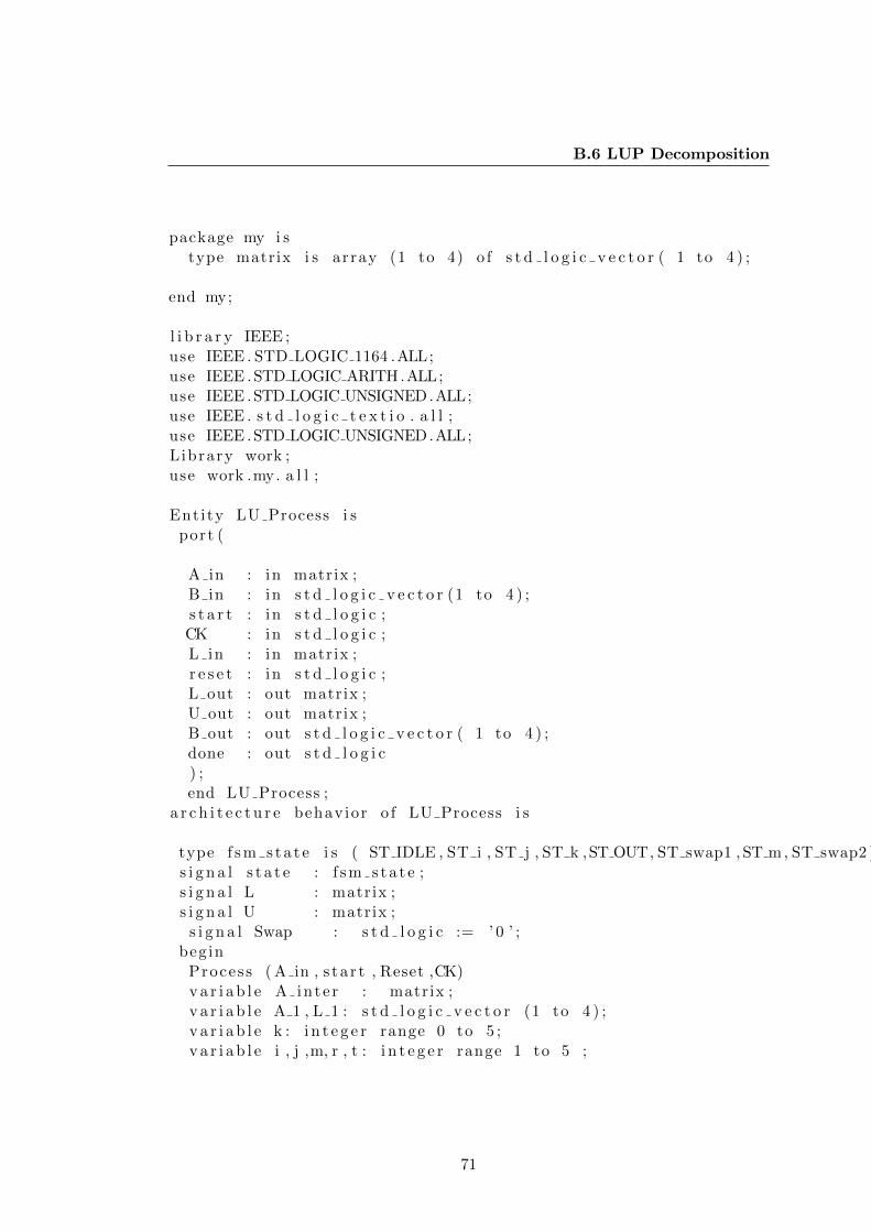
B.6 LUP Decomposition
package my i stype matrix i s array (1 to 4) o f s t d l o g i c v e c t o r ( 1 to 4 ) ;
end my;
l i b r a r y IEEE ;use IEEE . STD LOGIC 1164 .ALL;use IEEE . STD LOGIC ARITH .ALL;use IEEE .STD LOGIC UNSIGNED.ALL;use IEEE . s t d l o g i c t e x t i o . a l l ;use IEEE .STD LOGIC UNSIGNED.ALL;Library work ;use work .my. a l l ;
Ent ity LU Process i sport (
A in : in matrix ;B in : in s t d l o g i c v e c t o r (1 to 4 ) ;s t a r t : in s t d l o g i c ;CK : in s t d l o g i c ;L in : in matrix ;r e s e t : in s t d l o g i c ;L out : out matrix ;U out : out matrix ;B out : out s t d l o g i c v e c t o r ( 1 to 4 ) ;done : out s t d l o g i c) ;end LU Process ;
a r c h i t e c t u r e behavior o f LU Process i s
type f s m s t a t e i s ( ST IDLE , ST i , ST j , ST k ,ST OUT, ST swap1 , ST m, ST swap2 ) ;s i g n a l s t a t e : f s m s t a t e ;s i g n a l L : matrix ;s i g n a l U : matrix ;
s i g n a l Swap : s t d l o g i c := ’ 0 ’ ;begin
Process ( A in , s t a r t , Reset ,CK)v a r i a b l e A inte r : matrix ;v a r i a b l e A 1 , L 1 : s t d l o g i c v e c t o r (1 to 4 ) ;v a r i a b l e k : i n t e g e r range 0 to 5 ;v a r i a b l e i , j ,m, r , t : i n t e g e r range 1 to 5 ;
71
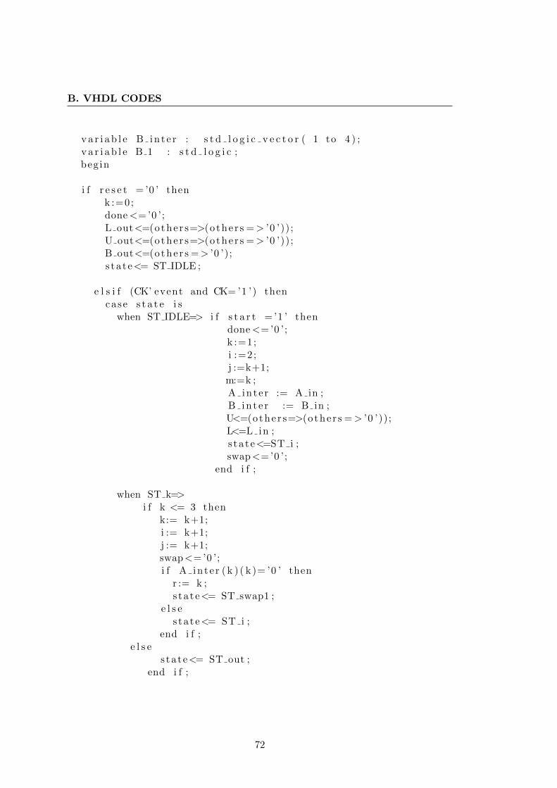
B. VHDL CODES
v a r i a b l e B in t e r : s t d l o g i c v e c t o r ( 1 to 4 ) ;v a r i a b l e B 1 : s t d l o g i c ;begin
i f r e s e t = ’0 ’ thenk :=0;done<= ’0 ’;L out<=(othe r s=>(o the r s => ’0 ’));U out<=(othe r s=>(o the r s => ’0 ’));B out<=(othe r s => ’0 ’);s ta te<= ST IDLE ;
e l s i f (CK’ event and CK= ’1 ’) thencase s t a t e i s
when ST IDLE=> i f s t a r t = ’1 ’ thendone<= ’0 ’;k :=1;i :=2;j :=k+1;m:=k ;A inte r := A in ;B in t e r := B in ;U<=(othe r s=>(o the r s => ’0 ’));L<=L in ;s ta te<=ST i ;swap<= ’0 ’;
end i f ;
when ST k=>i f k <= 3 then
k:= k+1;i := k+1;j := k+1;swap<= ’0 ’;i f A inte r ( k ) ( k )= ’0 ’ then
r := k ;s ta te<= ST swap1 ;
e l s es ta te<= ST i ;
end i f ;e l s e
s ta te<= ST out ;end i f ;
72

B.6 LUP Decomposition
when ST swap1 =>i f swap= ’0 ’ and A inte r ( r ) ( k )= ’1 ’ then
swap<= ’1 ’;A 1:= A inte r ( r ) ;B 1:= B inte r ( r ) ;A inte r ( r ):= A inte r ( k ) ;B in t e r ( r ):= B int e r ( k ) ;A inte r ( k):=A 1 ;B in t e r ( k):= B 1 ;L 1 := L( r ) ;t :=1;
s ta te<=st swap2 ;e l s e
i f r<=3 thenr := r +1;
s ta te<=st swap1 ;end i f ;
end i f ;When ST swap2 =>L( r ) ( t)<=L( k ) ( t ) ;L( k ) ( t)<=L 1 ( t ) ;
i f t< k−1 thent := t +1;
s ta te<=ST swap2 ;e l s e
s ta te<=ST i ;end i f ;
when ST i=>i f i<=4 thenL( i ) ( k)<= A inte r ( i ) ( k ) ;i f A inte r ( i ) ( k )= ’0 ’ then
s tate<= ST i ;i := i +1;
e l s ej := k+1;s ta te<= ST j ;
end i f ;e l s e
73
B. VHDL CODES
m:=k ;s ta te<=ST m ;
end i f ;
When ST j =>A inte r ( i ) ( j ):= A inte r ( i ) ( j ) XOR ( L( i ) ( k ) and A inte r ( k ) ( j ) ) ;
i f j<=3 thenstate<=ST j ;j := j +1;
e l s ei := i +1;s ta te<=s t i ;
end i f ;
When ST m =>
U( k ) (m)<= A inte r ( k ) (m) ;
i f m<=3 thenm:=m+1;s ta te<=st m ;
e l s e
s ta te<=ST k ;end i f ;
when ST OUT=>
L out<=L ;U out<=U;
74

B.6 LUP Decomposition
B out<=B inte r ;done <= ’1 ’;
end case ;
end i f ;end proce s s ;
end behavior ;
75

B. VHDL CODES
76

Bibliography
[1] A5/1. Data retrieved from http://en.wikipedia.org/wiki/A5/1. xi, 1
[2] Jacobi method. Data retrieved from http://en.wikipedia.org/wiki/Jacob method,. 6
[3] Lu decomposition. Data retrieved from http://en.wikipedia.org/wiki/LU decomposition.
41
[4] Phillip E. Allen and Douglas R. Holberg. CMOS analog circuit design. New York : Oxford
University Press, 2nd edition, 2002. 14, 19
[5] Do Danh CUONG, Zhi-Yuan CUI, Nam-Soo KIM, and Kie-Yong LEE. Low power 8-b
cmos current steering folding-interpolating a/d converter. IEICE TRANS. ELECTRON.,
E91C(1). ix, 10
[6] Benedik Driessen. Towards solving the linear equations in z2 in the analog domain. 8
March 2010. 2
[7] Benedikt Driessen and Christof Paar. Christof paar, solving binary linear equation systems
using analog hardware. January 2011. ix, 1, 5, 8, 9
[8] Burak Erbagc. Linear equation solver using cmos technology. 2010. 33, 38
[9] Michael P. Flynn and David J. Allstot. Cmos folding a/d converters with current-mode
interpolation. IEEE JOURNAL OF SOLID-STATE CIRCUITS, 31(9), SEPTEMBER
1996. 10
[10] Alexander Huemer and Michael Schwabl. Security aspects in mobile telco networks. Sum-
mer semester 2010. ix, 1, 2
[11] Song Liu. Design of a cmos 6-bit folding and interpolating analog-to-digital converter. July
1999. ix, 11
[12] Zhen Liu, Yuan Wang, Song Jia, Lijiu Ji, and Xing Zhang. Low-power cmos folding and
interpolating adc with a fully-folding technique. Oct. 2007. 17
[13] Behzad Razavi. Design of Analog CMOS Integrated Circuits. McGraw-Hil, 2001. 13
77

BIBLIOGRAPHY
[14] Andy Rupp, Thomas Eisenbarth, Andrey Bogdanov, and Oliver Grieb. Hardware sle
solvers : Efficient building blocks for cryptographic and cryptanalytic applications. October
2010. 5
[15] Rabia Tugce Yazcgil. Analog equation solver implantation. 2010. 1
78

Declaration
I herewith declare that I have produced this paper without the prohibited
assistance of third parties and without making use of aids other than those
specified; notions taken over directly or indirectly from other sources have
been identified as such. This paper has not previously been presented in
identical or similar form to any other examination.
The thesis work was done from March 2011 to August 2011.
Mingyi Zhang,