design example report - power integrations | home · pdf file · 2016-03-28design...
TRANSCRIPT

Power Integrations
5245 Hellyer Avenue, San Jose, CA 95138 USA. Tel: +1 408 414 9200 Fax: +1 408 414 9201
www.powerint.com
Design Example Report
Summary and Features Low profile design, <10 mm component height
o Allows driver board to sit behind LEDs giving uniform illumination in a T8 replacement tube application
Superior performance and end user experience o Clean monotonic start-up – no output blinking o Fast start-up (<200 ms) – no perceptible delay
Highly energy efficient o ≥86% at 115 VAC and ≥87% at 230 VAC
Low cost, low component count and small printed circuit board footprint solution o No current sensing required o Frequency jitter for smaller, lower cost EMI filter components
Integrated protection and reliability features o Output open circuit / output short-circuit protection with auto-recovery o Line input overvoltage shutdown extends voltage withstand during line faults o Auto-recovering thermal shutdown with large hysteresis protects both components
and printed circuit board o No damage during brown-out or brown-in conditions
Meets IEC 61000-3-2 Class C harmonics and EN55015 B conducted EMI
Title High Efficiency (≥85%), High Power Factor (>0.9) 15 W T8 Isolated LED Driver Using LinkSwitchTM-PH LNK406EG
Specification 90 VAC – 265 VAC Input; 50 V, 0.3 A Output
Application LED Driver for T8 Lamp
Author Applications Engineering Department
Document Number
DER-256
Date October 7, 2010
Revision 1.2

DER-256 15 W T8 LED Driver Using LNK406EG 07-Oct-10
Page 2 of 35
Power Integrations Tel: +1 408 414 9200 Fax: +1 408 414 9201 www.powerint.com
PATENT INFORMATION The products and applications illustrated herein (including transformer construction and circuits external to the products) may be covered by one or more U.S. and foreign patents, or potentially by pending U.S. and foreign patent applications assigned to Power Integrations. A complete list of Power Integrations' patents may be found at www.powerint.com. Power Integrations grants its customers a license under certain patent rights as set forth at <http://www.powerint.com/ip.htm>.

07-Oct-10 DER-256 15 W T8 LED Driver Using LNK406EG
Page 3 of 35
Power Integrations Tel: +1 408 414 9200 Fax: +1 408 414 9201
www.powerint.com
Table of Contents 1 Introduction .................................................................................................................4 2 Power Supply Specification ........................................................................................6 3 Schematic ...................................................................................................................7 4 Circuit Description.......................................................................................................8
4.1 Input EMI Filtering and Protection........................................................................8 4.2 LinkSwitch-PH Primary ........................................................................................8
4.2.1 Bias Winding and Output OVP Sense ..........................................................9 4.3 Output Voltage Sense..........................................................................................9 4.4 Output Rectification .............................................................................................9
5 PCB Layout...............................................................................................................10 6 Bill of Materials .........................................................................................................12 7 Transformer Specification .........................................................................................14
7.1 Electrical Diagram..............................................................................................14 7.2 Electrical Specifications .....................................................................................14 7.3 Materials ............................................................................................................14 7.4 Transformer Build Diagram................................................................................15 7.5 Transformer Construction ..................................................................................15
8 Transformer Design Spreadsheet.............................................................................16 9 Performance Data.....................................................................................................19
9.1 Efficiency vs. Line ..............................................................................................19 9.2 Constant Current vs. Line ..................................................................................21 9.3 Power Factor vs. Line, Full Load .......................................................................22
10 Thermal Performance............................................................................................24 11 Harmonic Data ......................................................................................................26 12 Waveforms ............................................................................................................28
12.1 Input Line Voltage and Current ..........................................................................28 12.2 Drain Voltage and Current .................................................................................28 12.3 Output Voltage and Ripple Current....................................................................29 12.4 Drain Voltage and Current Start-up Profile ........................................................29 12.5 Output Current and Drain Voltage at Shorted Output ........................................30 12.6 Open Load Output Voltage ................................................................................30
13 Conducted EMI .....................................................................................................31 14 Radiated EMI ........................................................................................................33 15 Revision History ....................................................................................................34 Important Note: Although this board is designed to satisfy safety isolation requirements, the engineering prototype has not been agency approved. Therefore, all testing should be performed using an isolation transformer to provide the AC input to the prototype board.

DER-256 15 W T8 LED Driver Using LNK406EG 07-Oct-10
Page 4 of 35
Power Integrations Tel: +1 408 414 9200 Fax: +1 408 414 9201 www.powerint.com
1 Introduction The document describes a power factor corrected LED driver designed to drive a nominal LED string voltage of 50 V at 0.3 A from an input voltage range of 90 VAC to 265 VAC. The LED driver uses the LNK406EG from the LinkSwitch-PH family by Power Integrations. LinkSwitch-PH ICs allow the implementation of cost effective and low component count LED drivers which meet both power factor and harmonics limits; and also offer an enhanced end user experience. This includes ultra-wide dimming range (not used in this demo), flicker free operation (even with low cost AC line TRIAC dimmers) and fast, clean turn on. The topology used is an isolated flyback operating in continuous conduction mode. Output current regulation is sensed entirely from the primary side eliminating the need for secondary side feedback components. No external current sensing is required on the primary side either as this is performed inside the IC further reducing components and losses. The internal controller adjusts the MOSFET duty cycle to maintain a sinusoidal input current and therefore high power factor and low harmonic currents. The LNK406EG also provides a sophisticated range of protection features including auto-restart for open control loop and output short-circuit conditions. Line overvoltage provides extended line fault and surge withstand, output overvoltage protects the supply should the load be disconnect and accurate hysteretic thermal shutdown ensures safe average PCB temperatures under all conditions. The key goals of this design were low profile and high efficiency. This was to allow the driver board to fit into the space behind the LED load board inside a T8 tube and operate with an acceptable temperature rise. This necessitated careful selection of components and mounting methods but was simpler than alternate solutions due to the low component count required for a primary side regulated LinkSwitch-PH design. This document contains the LED driver specification, schematic, PCB diagram, bill of materials, transformer documentation and typical performance characteristics.

07-Oct-10 DER-256 15 W T8 LED Driver Using LNK406EG
Page 5 of 35
Power Integrations Tel: +1 408 414 9200 Fax: +1 408 414 9201
www.powerint.com
Fig
ure
1 –
Pop
ulat
ed C
ircui
t Boa
rd P
hoto
grap
h (T
op V
iew
).
Fig
ure
2 –
Pop
ulat
ed C
ircui
t Boa
rd P
hoto
grap
h (B
otto
m V
iew
), B
oard
Dim
ensi
ons
260.
44 m
m x
19.
53 m
m
F
igu
re 3
– C
ompo
nent
Hei
ght (
10 m
m).
DER-256 15 W T8 LED Driver Using LNK406EG 07-Oct-10
Page 6 of 35
Power Integrations Tel: +1 408 414 9200 Fax: +1 408 414 9201 www.powerint.com
2 Power Supply Specification The table below represents the minimum acceptable performance of the design. Actual performance is listed in the results section.
Description Symbol Min Typ Max Units Comment
Input Voltage VIN 90 115/230 265 VAC 2 Wire – no P.E.
Frequency fLINE 47 50/60 64 Hz
Output
Output Voltage VOUT 45 50 55 V
Output Current IOUT 0.3 A
Total Output Power
Continuous Output Power POUT 15 W
Efficiency
Full Load 85 % Measured at 115 / 230 VAC
Environmental
Conducted EMI Meets CISPR 15B / EN55015B
Radiated EMI FCC Class B / EN55015
Safety Designed to meet IEC950 / UL1950 Class II
Power Factor 0.9 Measured at VOUT(TYP), IOUT(TYP) and 115 VAC / 230 VAC
Harmonics EN 61000-3-2 Class C and D
Board Dimensions 260.44 x 19.53 x 13 (10) mm
Designed to fit behind LED load board in T8 tube. 13 mm total height including PCB and load protrusions, 10 mm max component height above PCB
Ambient Temperature TAMB 40 oC Free convection, sea level

07-Oct-10 DER-256 15 W T8 LED Driver Using LNK406EG
Page 7 of 35
Power Integrations Tel: +1 408 414 9200 Fax: +1 408 414 9201
www.powerint.com
3 Schematic
Figure 4 – Schematic.

DER-256 15 W T8 LED Driver Using LNK406EG 07-Oct-10
Page 8 of 35
Power Integrations Tel: +1 408 414 9200 Fax: +1 408 414 9201 www.powerint.com
4 Circuit Description The LinkSwitch-PH device is an integrated controller plus 725 V power MOSFET intended for use in LED driver applications. The LinkSwitch-PH is configured for use in a single-stage continuous conduction mode flyback topology and provides a primary side regulated constant current isolated output while maintaining high power factor from the AC input.
4.1 Input EMI Filtering and Protection Fuse F1 provides protection from catastrophic component failure while RV1 (MOV) provides a clamp to limit the maximum component voltage stress during differential line surges. The use of a MOV is more critical in this design as the value of input capacitance is low. The low value of capacitance results in a much larger increase in the rectified bus voltage (across C2) for a given differential surge level. A 275 VAC rated part was selected, being slightly above the maximum specified operating voltage of 265 VAC. Diode bridge BR1 rectifies the AC line voltage with capacitor C2 providing a low impedance path (decoupling) for the primary switching current. A low value of capacitance (sum of C1, C2 and C3) is necessary to maintain a power factor of greater than 0.9. EMI filtering is provided by inductors L1, L2, L3 and L4, C1 and Y1 safety rated C8. Resistor R1, R2 and R3 across L2, L3 and L4 dampen any resonance between the input inductors, capacitors and the AC line impedance which would otherwise be measured as increased conducted EMI.
4.2 LinkSwitch-PH Primary
Diode D1 and C3 detect the peak AC line voltage. This voltage is converted to a current which is fed into the V pin via R5, R6 and R7. This current is also used by the device to set the input over/under voltage protection thresholds. The V pin current and the FB pin current are used internally to control the average output LED current. The non-dimming mode of LinkSwitch was selected via a 24.9 k resistor on the R pin. In the non-dimming configuration LinkSwitch-PH is optimized for line regulation, maintaining a fixed output current across the entire input voltage range. Resistor R8 also sets the internal references to select the brown-in and brown-out and input overvoltage protection thresholds. Resistor R7 provides further line compensation and in this design achieves line regulation of ±3%. One end of the flyback transformer is connected to the DC bus while the other is driven by the integrated 725 V power MOSFET within U1. During the power MOSFET on time the primary current ramps up, storing energy in the transformer. This energy is transferred to the secondary when the power MOSFET turns off. An EER25 core was selected for low profile and used a triple insulated secondary winding with flying leads to meet safety spacing requirements.
07-Oct-10 DER-256 15 W T8 LED Driver Using LNK406EG
Page 9 of 35
Power Integrations Tel: +1 408 414 9200 Fax: +1 408 414 9201
www.powerint.com
Diode D2, R17, C12 and R18 clamp the drain voltage to a safe level due to the effect of a leakage inductance voltage spike seen on the drain at turn off. Diode D3 is necessary to prevent reverse current from flowing through the LinkSwitch-PH device when the voltage across the primary (VOR or flyback voltage), exceeds the voltage across C2 and the instantaneous input AC sine wave.
4.2.1 Bias Winding and Output OVP Sense
Diode D5, C5, R13 and R11 create a supply from the bias winding on the transformer. This voltage supplies the operating current into the BYPASS pin of U1 through D4 and R9. Capacitor C4 provides local decoupling for the BYPASS pin. It is also used during startup, being charged to ~6 V from an internal high-voltage current source tied to the device DRAIN pin. Once charged the energy stored is used to operate U1 until the output reaches regulation. Diode D6, R16, C7, R14, VR2, C6, R12, and Q1 provide an open load overvoltage protection function. Should the output load be disconnected then the output voltage increases, also causing the bias voltage to rise and therefore the voltage across C7. A separate diode and lower value capacitor are used to rectify the bias winding (D6 and C7) to reduce the delay before OV is triggered and therefore limit the maximum output voltage. Once the voltage across C7 exceeds the threshold set by VR2 (~33 V) Q1 is biased on, reducing the current into the FB pin to below the auto-restart threshold. Once auto-restart mode is entered switching is alternately disabled and enabled keeping the output voltage within acceptable limits until the load is reconnected. This protects output capacitors, C9 and C10 from excessive voltage should the load be disconnected e.g. during manufacturing testing.
4.3 Output Voltage Sense
A current proportional to the output voltage is fed into the FEEDBACK pin through R10 from the primary bias supply. This current together with the V pin current is used to maintain the average output current to be constant with changes in input and output voltage.
4.4 Output Rectification
Diode D7 rectifies the secondary winding while capacitors C9 and C10 filter the output. A small pre-load is provided by R15 which limits the output voltage under no-load conditions. Inductor L5 is used to reduce radiated EMI.

DER-256 15 W T8 LED Driver Using LNK406EG 07-Oct-10
Page 10 of 35
Power Integrations Tel: +1 408 414 9200 Fax: +1 408 414 9201 www.powerint.com
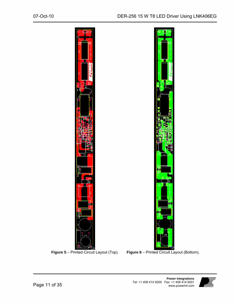
5 PCB Layout The PCB was designed such that the driver board can be placed directly behind the LED load PCB and still fit within a T8 tube. This required some specific considerations.
1 mm PCB thickness o Selected to increase height available for components
SMD component orientation o As the board was long and thin the board flexed significantly when handled.
To prevent component damage due to mechanical stress all SMD components were oriented on the board such that the long edge of the component is at 90 degrees to the long edge of the board.
SMD components on top side of PCB only o No SMD parts were placed on the bottom side of the PCB to reduce overall
board height – the low component count of LinkSwitch-PH solutions makes meeting this requirement much simpler.
07-Oct-10 DER-256 15 W T8 LED Driver Using LNK406EG
Page 11 of 35
Power Integrations Tel: +1 408 414 9200 Fax: +1 408 414 9201
www.powerint.com
Figure 5 – Printed Circuit Layout (Top). Figure 6 – Printed Circuit Layout (Bottom).

DER-256 15 W T8 LED Driver Using LNK406EG 07-Oct-10
Page 12 of 35
Power Integrations Tel: +1 408 414 9200 Fax: +1 408 414 9201 www.powerint.com
6 Bill of Materials Item Qty Ref Des Description Value
1 1 BR1 600 V, 1 A, Bridge Rectifier, Glass Passivated DB106S
2 1 C1 47 nF, 275 VAC, Film, X2 47 nF
3 1 C2 100 nF, 400 V, Film 100 nF
4 1 C3 1 F, 400 V, Electrolytic, (6.3 x 11) 1 F
5 1 C4 100 F, 25 V, Electrolytic, Low ESR, 130 m, (6.3 x 11) 100 F
6 1 C5 22 F, 50 V, Electrolytic, Low ESR, 900 m, (5 x 11.5) 22 F
7 2 C6 C11 100 nF, 50 V, Ceramic, X7R, 0805 100 nF
8 1 C7 1.0 F, 50 V, Ceramic, X7R, 1206 1.0 F
9 1 C8 2.2 nF, Ceramic, Y1 2.2 nF
10 2 C9 C10 100 F, 63, Electrolytic, Low ESR, 255 m, (10 x 12.5) 100 F
11 1 C12 1 nF, 1 kV, Disc Ceramic 1 nF
12 2 D1 D6 1000 V, 1 A, Rectifier, DO-41 1N4007
13 2 D2 D5 1000 V, 1 A, Fast Recovery,500 ns, DO-41 FR107
14 1 D3 200 V, 1 A, Ultrafast Recovery, 50 ns, DO-41 MUR120
15 1 D4 75 V, 0.15 A, Fast Switching, DO-35 LL4148
16 1 D7 600 V, 1 A, Ultrafast Recovery, 75 ns, DO-41 MUR160
17 1 F1 3.15 A, 250 V, Slow 3.15 A
18 1 L1 4 mH, 0.2 A, T13, U10000, 35 turns 4 mH
19 3 L2 L3 L4 1000 H, 0.18 A, 8 x 10 mm 1000 H
20 1 L5 300 H, 1 A, T8, U10000, 10turns 300 H
21 1 Q1 NPN,60 V 1000 MA, SOT-23 FMMT491
22 3 R1 R2 R3 4.7 k, 5%, 1/4 W, Carbon Film 4.7 k
23 1 R4 240 k, 5%, 1/4 W, Metal Film, 1206 240 k
24 1 R5 1.8 M, 1%, 1/4 W, Metal Film, 1206 1.8 M
25 1 R6 1.6 M, 1%, 1/4 W, Metal Film, 1206 1.6 M
26 1 R7 1.8 M, 1%, 1/8 W, Metal Film, 0805 1.8 M
27 1 R8 24.9 k, 1%, 1/4 W, Metal Film 24.9 k
28 1 R9 6.2 k, 5%, 1/8 W, Metal Film, 0805 6.2 k
29 1 R10 130 k, 1%, 1/8 W, Metal Film, 0805 130 k
30 1 R11 20 k, 5%, 1/8 W, Metal Film, 0805 20 k
31 1 R12 1 k, 5%, 1/8 W, Metal Film, 0805 1 k
32 1 R13 150 , 5%, 1/8 W, Carbon Film 150
33 1 R14 10 k, 5%, 1/8 W, Metal Film, 0805 10 k
34 1 R15 56 k, 5%, 1/4 W, Metal Film, 1206 56 k
35 1 R16 100 , 5%, 1/8 W, Metal Film, 0805 100
36 1 R17 100 , 5%, 1/4 W, Metal Film, 1206 100
37 1 R18 82 k, 5%, 1/2 W, Carbon Film 82 k
38 1 RV1 275 V, 80J, 10 mm, RADIAL 10D431

07-Oct-10 DER-256 15 W T8 LED Driver Using LNK406EG
Page 13 of 35
Power Integrations Tel: +1 408 414 9200 Fax: +1 408 414 9201
www.powerint.com
39 1 T1 EER25, special low profile, 5 + 5 EER2510
40 1 U1 LinkSwitch-PH, LNK406EG, eSIP LNK406EG
41 1 VR2 33 V, 5%, 500 mW, DO-213AA (MELF) ZMM5257B
DER-256 15 W T8 LED Driver Using LNK406EG 07-Oct-10
Page 14 of 35
Power Integrations Tel: +1 408 414 9200 Fax: +1 408 414 9201 www.powerint.com
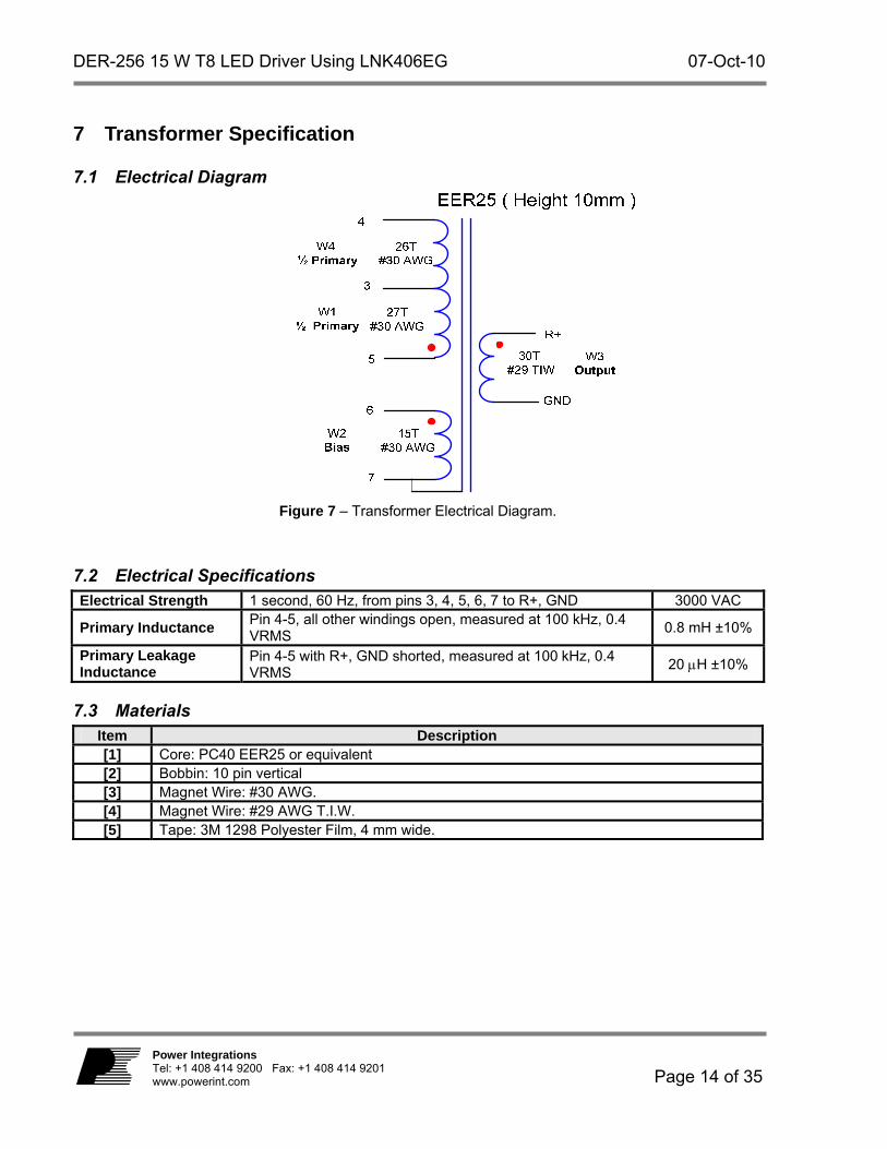
7 Transformer Specification
7.1 Electrical Diagram
Figure 7 – Transformer Electrical Diagram.
7.2 Electrical Specifications
7.3 Materials
Electrical Strength 1 second, 60 Hz, from pins 3, 4, 5, 6, 7 to R+, GND 3000 VAC
Primary Inductance Pin 4-5, all other windings open, measured at 100 kHz, 0.4 VRMS
0.8 mH ±10%
Primary Leakage Inductance
Pin 4-5 with R+, GND shorted, measured at 100kHz, 0.4 VRMS
20 H ±10%
Item Description [1] Core: PC40 EER25 or equivalent [2] Bobbin: 10 pin vertical [3] Magnet Wire: #30 AWG. [4] Magnet Wire: #29 AWG T.I.W. [5] Tape: 3M 1298 Polyester Film, 4 mm wide.
07-Oct-10 DER-256 15 W T8 LED Driver Using LNK406EG
Page 15 of 35
Power Integrations Tel: +1 408 414 9200 Fax: +1 408 414 9201
www.powerint.com
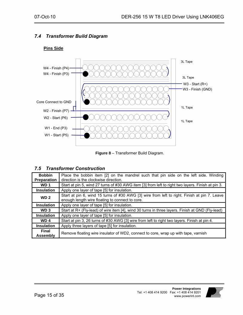
7.4 Transformer Build Diagram
Figure 8 – Transformer Build Diagram.
7.5 Transformer Construction
Bobbin Preparation
Place the bobbin item [2] on the mandrel such that pin side on the left side. Winding direction is the clockwise direction.
WD 1 Start at pin 5, wind 27 turns of #30 AWG item [3] from left to right two layers. Finish at pin 3. Insulation Apply one layer of tape [5] for insulation.
WD 2 Start at pin 6, wind 15 turns of #30 AWG [3] wire from left to right. Finish at pin 7. Leave enough length wire floating to connect to core.
Insulation Apply one layer of tape [5] for insulation. WD 3 Start at R+ (Fly-lead) of wire item [4], wind 30 turns in three layers. Finish at GND (Fly-lead)
Insulation Apply one layer of tape [5] for insulation. WD 4 Start at pin 3, 26 turns of #30 AWG [3] wire from left to right two layers. Finish at pin 4.
Insulation Apply three layers of tape [5] for insulation. Final
Assembly Remove floating wire insulator of WD2, connect to core, wrap up with tape, varnish
Pins Side
W1 - Start (P5)
W2 - Finish (P7)
W2 - Start (P6)
W3 - Start (R+)
W3 - Finish (GND)
1L Tape
1L Tape
3L Tape
W4 - Finish (P3)3L Tape
W1 - End (P3)
W4 - Finish (P4)
Core Connect to GND

DER-256 15 W T8 LED Driver Using LNK406EG 07-Oct-10
Page 16 of 35
Power Integrations Tel: +1 408 414 9200 Fax: +1 408 414 9201 www.powerint.com
8 Transformer Design Spreadsheet ACDC_LinkSwitch-
PH_061010; Rev.1.1; Copyright Power Integrations 2010 INPUT INFO OUTPUT UNIT
LinkSwitch-PH_061010: Flyback Transformer Design Spreadsheet
ENTER APPLICATION VARIABLES
Dimming required NO NO Select 'YES' option if dimming is required. Otherwise select 'NO'.
VACMIN 90 90 V Minimum AC Input Voltage VACMAX 265 265 V Maximum AC input voltage fL 50 Hz AC Mains Frequency VO 50.00 V Typical output voltage of LED string at full load VO_MAX 55.00 V Maximum expected LED string Voltage. VO_MIN 45.00 V Minimum expected LED string Voltage. V_OVP 60.50 V Over-voltage protection setpoint IO 0.30 Typical full load LED current PO 15.0 W Output Power n 0.80 0.8 Estimated efficiency of operation VB 20 20 V Bias Voltage ENTER LinkSwitch-PH VARIABLES LinkSwitch-PH LNK406 Universal 115 Doubled/230V Chosen Device LNK406 Power Out 22.5W 22.5W
Current Limit Mode FULL FULL Select "RED" for reduced Current Limit mode or "FULL" for Full current limit mode
ILIMITMIN 1.48 A Minimum current limit ILIMITMAX 1.69 A Maximum current limit fS 66000 Hz Switching Frequency fSmin 62000 Hz Minimum Switching Frequency fSmax 70000 Hz Maximum Switching Frequency IV 38.7 uA V pin current RV 3.909 M-ohms Upper V pin resistor RV2 1.402 M-ohms Lower V pin resistor IFB 130.00 130.0 uA FB pin current (85 uA < IFB < 210 uA) RFB1 130.8 k-ohms FB pin resistor
VDS 10 V LinkSwitch-PH on-state Drain to Source Voltage
VD 0.50 V Output Winding Diode Forward Voltage Drop (0.5 V for Schottky and 0.8 V for PN diode)
VDB 0.70 V Bias Winding Diode Forward Voltage Drop Key Design Parameters
KP 1.05 1.05 Ripple to Peak Current Ratio (For PF > 0.9, 0.4 < KP < 0.9)
LP 809 uH Primary Inductance VOR 90.00 90 V Reflected Output Voltage. Expected IO (average) 0.29 A Expected Average Output Current
KP_VACMAX Info 1.28 !!! Info. PF at high line may be less than 0.9. Decrease KP for higher PF
TON_MIN 1.62 us Minimum on time at maximum AC input voltage PCLAMP 0.11 W Estimated dissipation in primary clamp ENTER TRANSFORMER CORE/CONSTRUCTION VARIABLES Core Type EER2510 EER2510 Bobbin #N/A P/N: #N/A AE 0.5400 0.54 cm^2 Core Effective Cross Sectional Area LE 3.6000 3.6 cm Core Effective Path Length AL #N/A nH/T^2 Ungapped Core Effective Inductance BW 4.2 4.2 mm Bobbin Physical Winding Width
M 0 mm Safety Margin Width (Half the Primary to Secondary Creepage Distance)
L 4.00 4 Number of Primary Layers NS 30 30 Number of Secondary Turns DC INPUT VOLTAGE PARAMETERS VMIN 127 V Peak input voltage at VACMIN

07-Oct-10 DER-256 15 W T8 LED Driver Using LNK406EG
Page 17 of 35
Power Integrations Tel: +1 408 414 9200 Fax: +1 408 414 9201
www.powerint.com
VMAX 375 V Peak input voltage at VACMAX CURRENT WAVEFORM SHAPE PARAMETERS DMAX 0.42 Minimum duty cycle at peak of VACMIN IAVG 0.18 A Average Primary Current
IP 1.04 A Peak Primary Current (calculated at minimum input voltage VACMIN)
IRMS 0.31 A Primary RMS Current (calculated at minimum input voltage VACMIN)
TRANSFORMER PRIMARY DESIGN PARAMETERS LP 809 uH Primary Inductance NP 53 Primary Winding Number of Turns NB 12 Bias Winding Number of Turns ALG 283 nH/T^2 Gapped Core Effective Inductance
BM 2917 Gauss Maximum Flux Density at PO, VMIN (BM<3100)
BP 3530 Gauss Peak Flux Density (BP<3700)
BAC 1459 Gauss AC Flux Density for Core Loss Curves (0.5 X Peak to Peak)
ur #N/A Relative Permeability of Ungapped Core LG #N/A #N/A mm #N/A BWE 16.8 mm Effective Bobbin Width
OD 0.31 mm Maximum Primary Wire Diameter including insulation
INS 0.05 mm Estimated Total Insulation Thickness (= 2 * film thickness)
DIA 0.26 mm Bare conductor diameter
AWG 30 AWG Primary Wire Gauge (Rounded to next smaller standard AWG value)
CM 102 Cmils Bare conductor effective area in circular mils
CMA 325 Cmils/Amp Primary Winding Current Capacity (200 < CMA < 600)
LP_TOL 10 Tolerance of primary inductance TRANSFORMER SECONDARY DESIGN PARAMETERS (SINGLE OUTPUT EQUIVALENT) Lumped parameters ISP 1.86 A Peak Secondary Current ISRMS 0.60 A Secondary RMS Current IRIPPLE 0.52 A Output Capacitor RMS Ripple Current
CMS 120 Cmils Secondary Bare Conductor minimum circular mils
AWGS 29 AWG Secondary Wire Gauge (Rounded up to next larger standard AWG value)
DIAS 0.29 mm Secondary Minimum Bare Conductor Diameter
ODS 0.14 mm Secondary Maximum Outside Diameter for Triple Insulated Wire
VOLTAGE STRESS PARAMETERS
VDRAIN 563 V Estimated Maximum Drain Voltage assuming maximum LED string voltage (Includes Effect of Leakage Inductance)
PIVS 271 V Output Rectifier Maximum Peak Inverse Voltage (calculated at VOVP, excludes leakage inductance spike)
PIVB 110 V Bias Rectifier Maximum Peak Inverse Voltage (calculated at VOVP, excludes leakage inductance spike)
FINE TUNING (Enter measured values from prototype) V pin Resistor Fine Tuning RV1 3.91 M-ohms Upper V Pin Resistor Value RV2 1.40 M-ohms Lower V Pin Resistor Value VAC1 115.0 V Test Input Voltage Condition1 VAC2 230.0 V Test Input Voltage Condition2 IO_VAC1 0.30 A Measured Output Current at VAC1 IO_VAC2 0.30 A Measured Output Current at VAC2 RV1 (new) 3.91 M-ohms New RV1 RV2 (new) 1.40 M-ohms New RV2
V_OV 318.3 V Typical AC input voltage at which OV shutdown will be triggered

DER-256 15 W T8 LED Driver Using LNK406EG 07-Oct-10
Page 18 of 35
Power Integrations Tel: +1 408 414 9200 Fax: +1 408 414 9201 www.powerint.com
V_UV 70.8 V Typical AC input voltage beyond which power supply can startup
FB pin resistor Fine Tuning RFB1 131 k-ohms Upper FB Pin Resistor Value RFB2 1E+012 k-ohms Lower FB Pin Resistor Value VB1 18.0 V Test Bias Voltage Condition1 VB2 22.0 V Test Bias Voltage Condition2 IO1 0.30 A Measured Output Current at Vb1 IO2 0.30 A Measured Output Current at Vb2 RFB1 (new) 130.8 k-ohms New RFB1 RFB2(new) 1.00E+12 k-ohms New RFB2
Note: Actual values used for RV1 = 3.4 M, RV2 = 1.8 M. Measured PF at 230 VAC was 0.9.
07-Oct-10 DER-256 15 W T8 LED Driver Using LNK406EG
Page 19 of 35
Power Integrations Tel: +1 408 414 9200 Fax: +1 408 414 9201
www.powerint.com
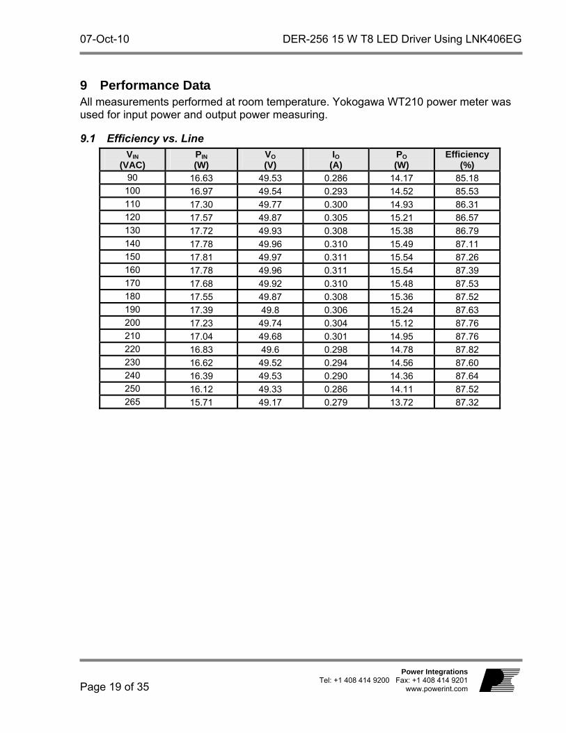
9 Performance Data All measurements performed at room temperature. Yokogawa WT210 power meter was used for input power and output power measuring.
9.1 Efficiency vs. Line
VIN (VAC)
PIN (W)
VO
(V) IO
(A) PO (W)
Efficiency (%)
90 16.63 49.53 0.286 14.17 85.18 100 16.97 49.54 0.293 14.52 85.53 110 17.30 49.77 0.300 14.93 86.31 120 17.57 49.87 0.305 15.21 86.57 130 17.72 49.93 0.308 15.38 86.79 140 17.78 49.96 0.310 15.49 87.11 150 17.81 49.97 0.311 15.54 87.26 160 17.78 49.96 0.311 15.54 87.39 170 17.68 49.92 0.310 15.48 87.53 180 17.55 49.87 0.308 15.36 87.52 190 17.39 49.8 0.306 15.24 87.63 200 17.23 49.74 0.304 15.12 87.76 210 17.04 49.68 0.301 14.95 87.76 220 16.83 49.6 0.298 14.78 87.82 230 16.62 49.52 0.294 14.56 87.60 240 16.39 49.53 0.290 14.36 87.64 250 16.12 49.33 0.286 14.11 87.52 265 15.71 49.17 0.279 13.72 87.32

DER-256 15 W T8 LED Driver Using LNK406EG 07-Oct-10
Page 20 of 35
Power Integrations Tel: +1 408 414 9200 Fax: +1 408 414 9201 www.powerint.com
85.0
85.5
86.0
86.5
87.0
87.5
88.0
85 100 115 130 145 160 175 190 205 220 235 250 265 280
Input Voltage (VAC)
Eff
icie
ncy
(%
)
Figure 9 – Efficiency vs. Input Voltage, Room Temperature.
07-Oct-10 DER-256 15 W T8 LED Driver Using LNK406EG
Page 21 of 35
Power Integrations Tel: +1 408 414 9200 Fax: +1 408 414 9201
www.powerint.com
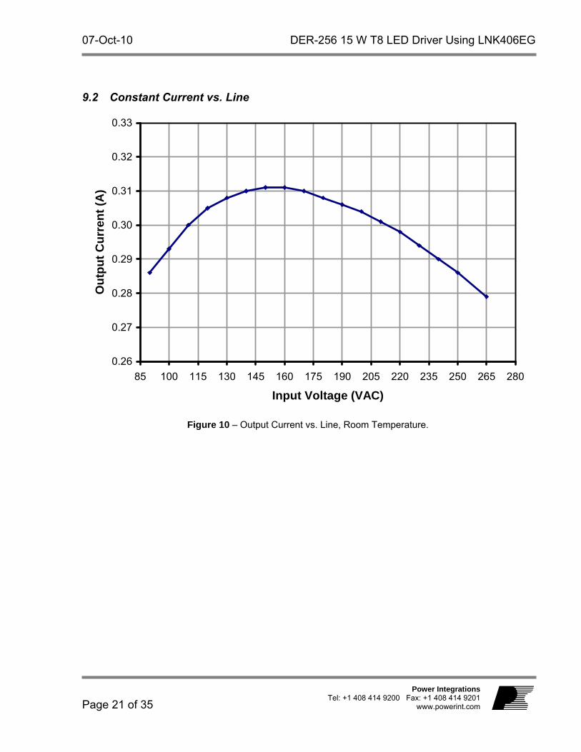
9.2 Constant Current vs. Line
0.26
0.27
0.28
0.29
0.30
0.31
0.32
0.33
85 100 115 130 145 160 175 190 205 220 235 250 265 280
Input Voltage (VAC)
Ou
tpu
t C
urr
ent
(A)
Figure 10 – Output Current vs. Line, Room Temperature.

DER-256 15 W T8 LED Driver Using LNK406EG 07-Oct-10
Page 22 of 35
Power Integrations Tel: +1 408 414 9200 Fax: +1 408 414 9201 www.powerint.com
9.3 Power Factor vs. Line, Full Load
VIN (VAC)
PIN (W)
VO
(V) IO
(A) PO (W)
PF
90 16.63 49.53 0.286 14.17 0.9796
100 16.97 49.54 0.293 14.52 0.9745
110 17.30 49.77 0.300 14.93 0.9715
120 17.57 49.87 0.305 15.21 0.9687
130 17.72 49.93 0.308 15.38 0.966
140 17.78 49.96 0.310 15.49 0.9638
150 17.81 49.97 0.311 15.54 0.9615
160 17.78 49.96 0.311 15.54 0.9592
170 17.68 49.92 0.310 15.48 0.9571
180 17.55 49.87 0.308 15.36 0.955
190 17.39 49.8 0.306 15.24 0.9528
200 17.23 49.74 0.304 15.12 0.9505
210 17.04 49.68 0.301 14.95 0.9484
220 16.83 49.6 0.298 14.78 0.9459
230 16.62 49.52 0.294 14.56 0.9431
240 16.39 49.53 0.290 14.36 0.9401
250 16.12 49.33 0.286 14.11 0.9362
265 15.71 49.17 0.279 13.72 0.9279
07-Oct-10 DER-256 15 W T8 LED Driver Using LNK406EG
Page 23 of 35
Power Integrations Tel: +1 408 414 9200 Fax: +1 408 414 9201
www.powerint.com
0.92
0.93
0.94
0.95
0.96
0.97
0.98
0.99
85 100 115 130 145 160 175 190 205 220 235 250 265 280
Input Voltage (VAC)
Po
wer
Fac
tor
Figure 11 – Power Factor vs. Input Voltage, Room Temperature, Full Load.

DER-256 15 W T8 LED Driver Using LNK406EG 07-Oct-10
Page 24 of 35
Power Integrations Tel: +1 408 414 9200 Fax: +1 408 414 9201 www.powerint.com
10 Thermal Performance Images captured after running for 30 minutes at room temperature (25 °C), full load (50 V, 0.3 A). This indicates a LinkSwitch-PH (U1) operating temperature of ~80°C at an external board ambient of 40°C. As U1 is the highest temperature component on the board it provides effective thermal protection for the entire system via its internal thermal shutdown. Since there are no components on the bottom side, all the data below are for the top side.
Figure 12 – 115 VAC EMI and Rectifier. Figure 13 – 230 VAC EMI and Rectifier.
Figure 14 – 115 VAC Main Switching and Transformer.
Figure 15 – 230 VAC Main Switching and Transformer.

07-Oct-10 DER-256 15 W T8 LED Driver Using LNK406EG
Page 25 of 35
Power Integrations Tel: +1 408 414 9200 Fax: +1 408 414 9201
www.powerint.com
Figure 16 – 115 VAC Output Rectifier. Figure 17 – 230 VAC Output Rectifier.
DER-256 15 W T8 LED Driver Using LNK406EG 07-Oct-10
Page 26 of 35
Power Integrations Tel: +1 408 414 9200 Fax: +1 408 414 9201 www.powerint.com
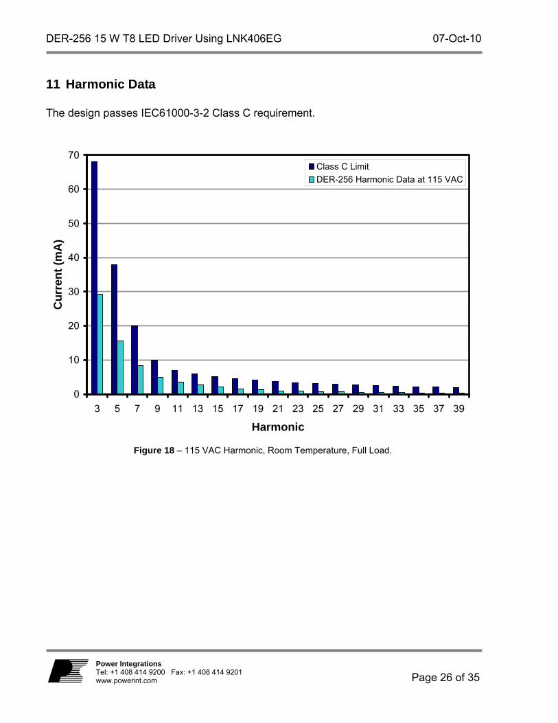
11 Harmonic Data The design passes IEC61000-3-2 Class C requirement.
0
10
20
30
40
50
60
70
3 5 7 9 11 13 15 17 19 21 23 25 27 29 31 33 35 37 39
Harmonic
Cu
rren
t (m
A)
Class C Limit
DER-256 Harmonic Data at 115 VAC
Figure 18 – 115 VAC Harmonic, Room Temperature, Full Load.

07-Oct-10 DER-256 15 W T8 LED Driver Using LNK406EG
Page 27 of 35
Power Integrations Tel: +1 408 414 9200 Fax: +1 408 414 9201
www.powerint.com
0
10
20
30
40
50
60
70
3 5 7 9 11 13 15 17 19 21 23 25 27 29 31 33 35 37 39
Harmonic
Cu
rren
t (m
A)
Class C Limit
DER-256 Harmonic Data at 230 VAC
Figure 19 – 230 VAC Harmonic, Room Temperature, Full Load.

DER-256 15 W T8 LED Driver Using LNK406EG 07-Oct-10
Page 28 of 35
Power Integrations Tel: +1 408 414 9200 Fax: +1 408 414 9201 www.powerint.com
12 Waveforms
12.1 Input Line Voltage and Current
12.2 Drain Voltage and Current
Figure 20 – 90 VAC, Full Load. Upper: IIN, 0.2 A / div. Lower: VIN, 100 V, 8 ms / div.
Figure 21 – 265 VAC, Full Load. Upper: IIN, 0.1 A / div. Lower: VIN, 500 V / div., 8 ms / div.
Figure 22 – 90 VAC, Full Load. Upper: IDRAIN, 0.5 A / div. Lower: VDRAIN, 100 V, 5 s / div.
Figure 23 – 265 VAC, Full Load. Upper: IDRAIN, 0.5 A / div. Lower: VDRAIN, 200 V / div., 5 s / div.
07-Oct-10 DER-256 15 W T8 LED Driver Using LNK406EG
Page 29 of 35
Power Integrations Tel: +1 408 414 9200 Fax: +1 408 414 9201
www.powerint.com
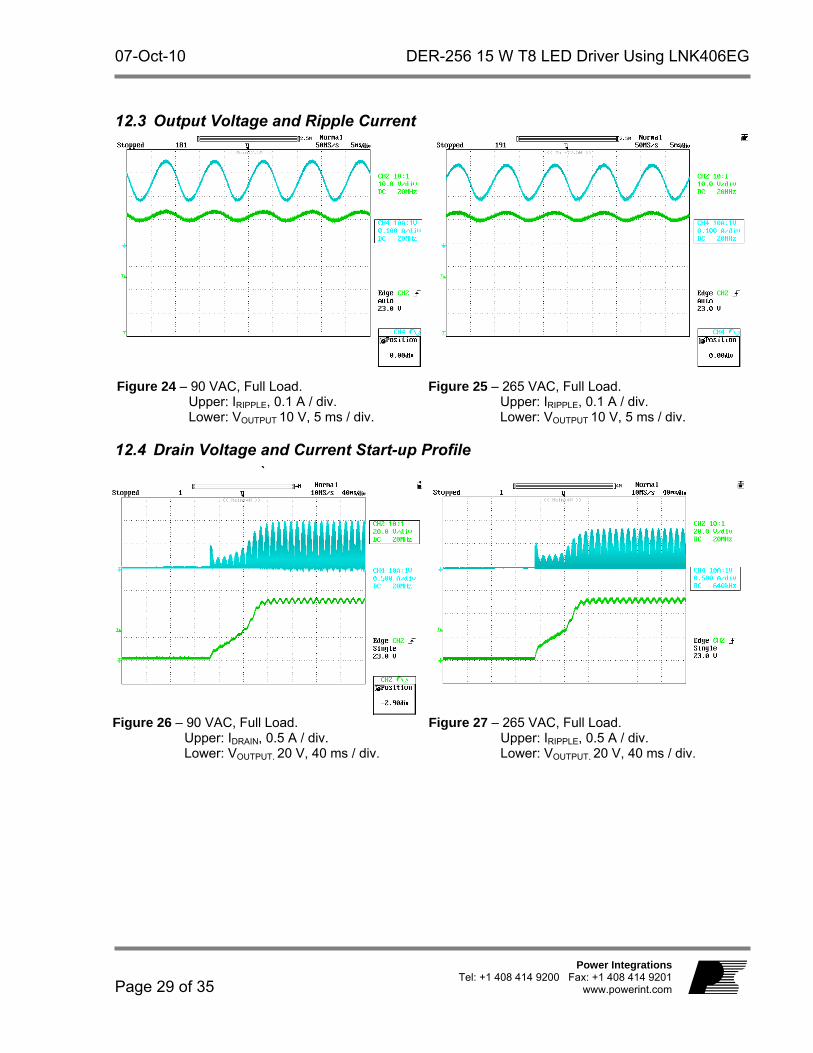
12.3 Output Voltage and Ripple Current
12.4 Drain Voltage and Current Start-up Profile
Figure 24 – 90 VAC, Full Load. Upper: IRIPPLE, 0.1 A / div. Lower: VOUTPUT 10 V, 5 ms / div.
Figure 25 – 265 VAC, Full Load. Upper: IRIPPLE, 0.1 A / div. Lower: VOUTPUT 10 V, 5 ms / div.
`
Figure 26 – 90 VAC, Full Load.
Upper: IDRAIN, 0.5 A / div. Lower: VOUTPUT, 20 V, 40 ms / div.
Figure 27 – 265 VAC, Full Load. Upper: IRIPPLE, 0.5 A / div. Lower: VOUTPUT, 20 V, 40 ms / div.

DER-256 15 W T8 LED Driver Using LNK406EG 07-Oct-10
Page 30 of 35
Power Integrations Tel: +1 408 414 9200 Fax: +1 408 414 9201 www.powerint.com
12.5 Output Current and Drain Voltage at Shorted Output
12.6 Open Load Output Voltage
Figure 28 – 90 VAC, Full Load. Upper: IOUTPUT, 1 A / div. Lower: VDRAIN, 100 V, 200 ms / div.
Figure 29 – 265 VAC, Full Load. Upper: IOUTPUT, 2 A / div. Lower: VDRAIN, 200 V, 200 ms / div.
Figure 30 – Output Voltage: 115 VAC. VOUT, 20 V / div., 500 ms / div.
Figure 31 – Output Voltage: 230 VAC. VOUT, 20 V / div., 500 ms / div.
07-Oct-10 DER-256 15 W T8 LED Driver Using LNK406EG
Page 31 of 35
Power Integrations Tel: +1 408 414 9200 Fax: +1 408 414 9201
www.powerint.com
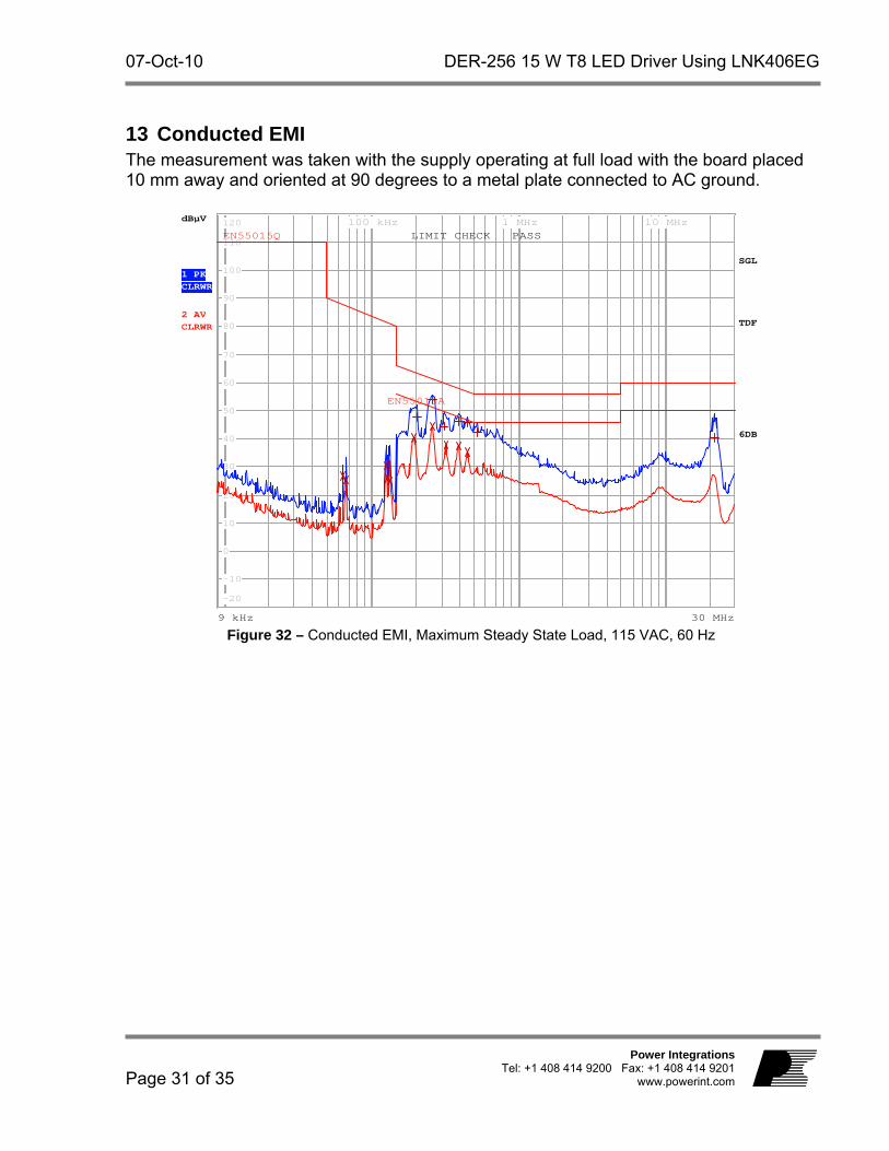
13 Conducted EMI The measurement was taken with the supply operating at full load with the board placed 10 mm away and oriented at 90 degrees to a metal plate connected to AC ground.
9 kHz 30 MHz
dBµV dBµV
1 PKCLRWR
6DB
2 AVCLRWR
SGL
TDF
100 kHz 1 MHz 10 MHz
-20
-10
0
10
20
30
40
50
60
70
80
90
100
110
120
LIMIT CHECK PASS
EN55015A
EN55015Q
Figure 32 – Conducted EMI, Maximum Steady State Load, 115 VAC, 60 Hz

DER-256 15 W T8 LED Driver Using LNK406EG 07-Oct-10
Page 32 of 35
Power Integrations Tel: +1 408 414 9200 Fax: +1 408 414 9201 www.powerint.com
9 kHz 30 MHz
dBµV dBµV
1 PKCLRWR
6DB
2 AVCLRWR
SGL
TDF
100 kHz 1 MHz 10 MHz
-20
-10
0
10
20
30
40
50
60
70
80
90
100
110
120
LIMIT CHECK PASS
EN55015A
EN55015Q
Figure 33 – Conducted EMI, Maximum Steady State Load, 230 VAC, 50 Hz.
07-Oct-10 DER-256 15 W T8 LED Driver Using LNK406EG
Page 33 of 35
Power Integrations Tel: +1 408 414 9200 Fax: +1 408 414 9201
www.powerint.com
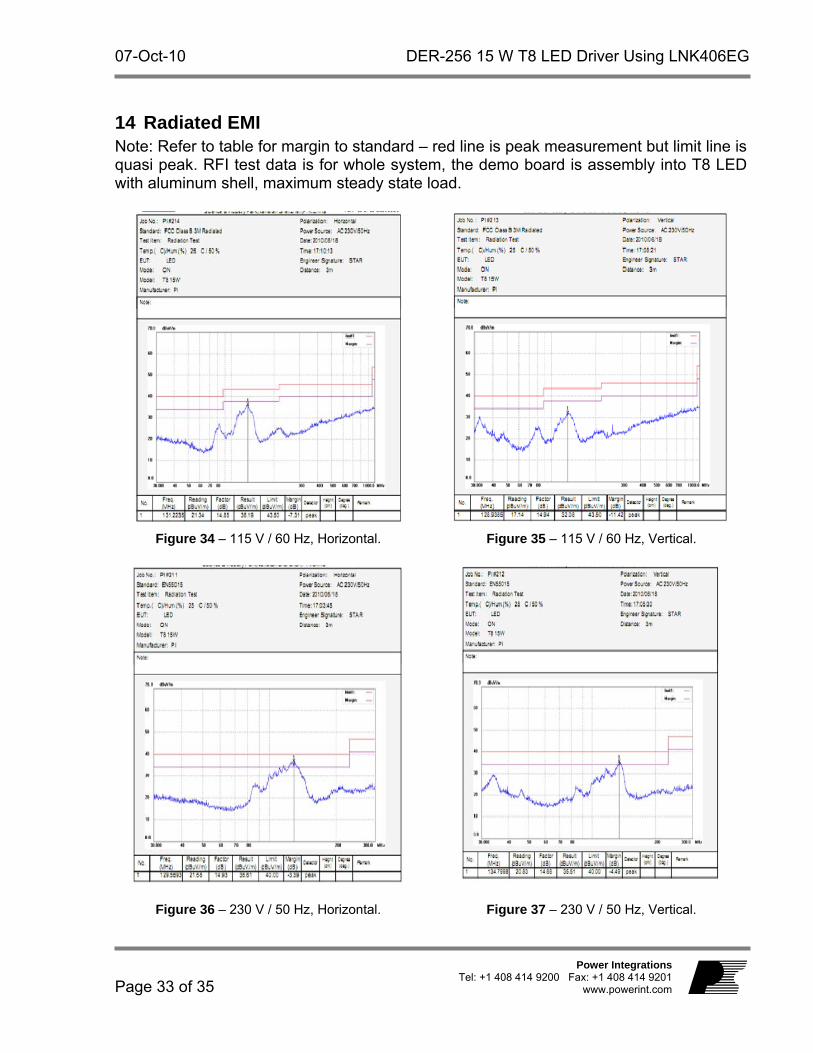
14 Radiated EMI Note: Refer to table for margin to standard – red line is peak measurement but limit line is quasi peak. RFI test data is for whole system, the demo board is assembly into T8 LED with aluminum shell, maximum steady state load.
Figure 34 – 115 V / 60 Hz, Horizontal. Figure 35 – 115 V / 60 Hz, Vertical.
Figure 36 – 230 V / 50 Hz, Horizontal. Figure 37 – 230 V / 50 Hz, Vertical.

DER-256 15 W T8 LED Driver Using LNK406EG 07-Oct-10
Page 34 of 35
Power Integrations Tel: +1 408 414 9200 Fax: +1 408 414 9201 www.powerint.com
15 Revision History
Date Author Revision Description & changes Reviewed 07-Oct-10 KM 1.2 Initial Release Apps & Mktg

07-Oct-10 DER-256 15 W T8 LED Driver Using LNK406EG
Page 35 of 35
Power Integrations Tel: +1 408 414 9200 Fax: +1 408 414 9201
www.powerint.com
For the latest updates, visit our website: www.powerint.com Power Integrations reserves the right to make changes to its products at any time to improve reliability or manufacturability. Power Integrations does not assume any liability arising from the use of any device or circuit described herein. POWER INTEGRATIONS MAKES NO WARRANTY HEREIN AND SPECIFICALLY DISCLAIMS ALL WARRANTIES INCLUDING, WITHOUT LIMITATION, THE IMPLIED WARRANTIES OF MERCHANTABILITY, FITNESS FOR A PARTICULAR PURPOSE, AND NON-INFRINGEMENT OF THIRD PARTY RIGHTS.
PATENT INFORMATION The products and applications illustrated herein (including transformer construction and circuits external to the products) may be covered by one or more U.S. and foreign patents, or potentially by pending U.S. and foreign patent applications assigned to Power Integrations. A complete list of Power Integrations’ patents may be found at www.powerint.com. Power Integrations grants its customers a license under certain patent rights as set forth at http://www.powerint.com/ip.htm. The PI Logo, TOPSwitch, TinySwitch, LinkSwitch, DPA-Switch, PeakSwitch, EcoSmart, Clampless, E-Shield, Filterfuse, StackFET, PI Expert and PI FACTS are trademarks of Power Integrations, Inc. Other trademarks are property of their respective companies. ©Copyright 2010 Power Integrations, Inc.
Power Integrations Worldwide Sales Support Locations
WORLD HEADQUARTERS 5245 Hellyer Avenue San Jose, CA 95138, USA. Main: +1-408-414-9200 Customer Service: Phone: +1-408-414-9665 Fax: +1-408-414-9765 e-mail: [email protected]
GERMANY Rueckertstrasse 3 D-80336, Munich Germany Phone: +49-89-5527-3911 Fax: +49-89-5527-3920 e-mail: [email protected]
JAPAN Kosei Dai-3 Building 2-12-11, Shin-Yokohama, Kohoku-ku, Yokohama-shi, Kanagawa 222-0033 Japan Phone: +81-45-471-1021 Fax: +81-45-471-3717 e-mail: [email protected]
TAIWAN 5F, No. 318, Nei Hu Rd., Sec. 1 Nei Hu District Taipei 114, Taiwan R.O.C. Phone: +886-2-2659-4570 Fax: +886-2-2659-4550 e-mail: [email protected]
CHINA (SHANGHAI) Rm 1601/1610, Tower 1 Kerry Everbright City No. 218 Tianmu Road West Shanghai, P.R.C. 200070 Phone: +86-021-6354-6323 Fax: +86-021-6354-6325 e-mail: [email protected]
INDIA #1, 14th Main Road Vasanthanagar Bangalore-560052 India Phone: +91-80-4113-8020 Fax: +91-80-4113-8023 e-mail: [email protected]
KOREA RM 602, 6FL Korea City Air Terminal B/D, 159-6 Samsung-Dong, Kangnam-Gu, Seoul, 135-728 Korea Phone: +82-2-2016-6610 Fax: +82-2-2016-6630 e-mail: [email protected]
UNITED KINGDOM 1st Floor, St. James’s House East Street, Farnham Surrey, GU9 7TJ United Kingdom Phone: +44 (0) 1252-730-141 Fax: +44 (0) 1252-727-689 e-mail: [email protected]
CHINA (SHENZHEN) Rm A, B & C 4th Floor, Block C, Electronics Science and Technology Building 2070 Shennan Zhong Road Shenzhen, Guangdong, P.R.C. 518031 Phone: +86-755-8379-3243 Fax: +86-755-8379-5828 e-mail: [email protected]
ITALY Via De Amicis 2 20091 Bresso MI Italy Phone: +39-028-928-6000 Fax: +39-028-928-6009 e-mail: [email protected]
SINGAPORE 51 Newton Road, #15-08/10 Goldhill Plaza Singapore, 308900 Phone: +65-6358-2160 Fax: +65-6358-2015 e-mail: [email protected]
APPLICATIONS HOTLINE World Wide +1-408-414-9660 APPLICATIONS FAX World Wide +1-408-414-9760