11w flyback converter_l6590
TRANSCRIPT

8/8/2019 11w Flyback Converter_l6590
http://slidepdf.com/reader/full/11w-flyback-converterl6590 1/24
1/24
AN1523
APPLICATION NOTE
March 2002
Introduction
Low power SMPS are today very popular in consumer applications for example like low-cost cable, terrestrialdecoders or high end TV chassis and the manufacturers need to design circuits with good performance, smallsize with high cost effectiveness. An integrated monolithic solution controlling the SMPS like the L6590 makesit a very suitable device, able to satisfy all the requirements of a compact and flexible solution, integrating all thenecessary functions to obtain a robust design just adding few external components. In this proposed referencedesign, the board is thru-hole technology, without any heat sink. A specific application circuit fully tested is pro-posed and the test results, including thermal and EMI, are enclosed in this document. The transformer data areincluded too, making it a good way to achieve a very short time to market solution.
SMPS Main characteristics
q INPUT AND OUTPUT VOLTAGES:
q
STAND BY:During the stand-by operation the power consumption from the mains has to be ≤1W, when the circuit
delivers 50mA from the 5V output and the 12V is unloaded.
q PROTECTIONS:
Overload ad short circuit on both outputs, with auto-restart at short removal. An OVP circuit for open-
loop protection.
q SAFETY:
In acc. with EN60065, creepage and clearance minimum distance is 4.8mm
q EMI:
In acc. with EN50022 Class B
INPUT VOLTAGE: OUTPUT VOLTAGES AT FULL LOAD:
Vout Iout Pout STABILITY
Vin: 90 ÷ 264 Vrms [V] [A] [W]
f: 45÷ 66 Hz 5 1.4 7.5 ±2%
12 0.3 3.6 ±5%
POUT (W) = 11.1
by Claudio Spini
11W FLYBACK CONVERTER FOR AUXILIARY POWERSUPPLY APPLICATION USING THE L6590
This document describes an 11W Switch Mode Power Supply reference design, dedicated to Consumer
Applications, e.g. TV chassis auxiliary power supply, low cost Set-top box or digital equipment. The
board accepts full range input voltage (90 to 265Vrms) and delivers 2 output voltages. It is based on the
monolithic controller L6590, integrating the controller and a POWERMOS and working at fixed frequen-
cy, PWM mode and including a stand-by function to minimize the power consumption during light load
operation. It incorporates also all the protections, offering a complete and very compact solution for low
power SMPS.
O b s o l e t e
P r o d u c
t ( s ) - O b s
o l e t e
P r o d u c
t ( s )

8/8/2019 11w Flyback Converter_l6590
http://slidepdf.com/reader/full/11w-flyback-converterl6590 2/24
O b s o l e t e
P r o d u c
t ( s ) - O b s
o l e t e
P r o d u c
t ( s )
AN1523 APPLICATION NOTE
2/24
Electrical diagram
The SMPS topology is the standard Fly-back, working in continuous mode at low input voltage. Core of thisSMPS is the L6590, a monolithic device integrating the controller and a 700V MOSFET, available in Minidip orSO-16 popular packages. In this design, the Minidip has been used. The switching frequency is fixed by aninternal oscillator at 65KHz during normal operation. When a light load is detected, the oscillator switches auto-matically to 22KHz, thus increasing the stand-by performance of the circuit. At start-up, the L6590 is activatedby an internal current source that draws current from the DC bus and charges the capacitor C2. Thanks to thiscircuit, the wake-up time is shorter than the conventional resistor solution and independent from the input mainsvoltage. The current source is internally disconnected after that the Vcc voltage has reached the VccON value,to prevent power dissipation during light load operation. During normal operation, the device is powered by thetransformer, via the diode D3. The network Q1, Q2, C6, R9, R10, R11 improves the circuit performance duringfaults. The components C3 and R2 belong to the feedback loop. The power dissipation of the L6590 is ensured
by a copper area on the bottom side of the printed circuit board.The transformer is a layer type, using Triple Insulation Wire for the secondary windings, manufactured by EL-DOR in accordance with the EN60065. The transformer reflected voltage is ~105V and the ferrite core size isa small, standard E20. The Transil D1 and the diode D2 clamp the peak of the leakage inductance voltage spikeat a safe level for the operation of the L6590, providing enough room for the leakage inductance voltage spikewith still margin for reliability.
The output rectifiers have been chosen in accordance with the maximum reverse voltage and their power dis-sipation. Standard, low-cost, axial, fast recovery rectifiers have been selected in order to avoid transformer frac-tional number of turns and to obtain the output voltage values as close as possible to the nominal ones. Ofcourse, using High-voltage Schottky rectifier the efficiency at full load would be higher but the cost and the out-put voltage precision would be adversely affected. A small LC filter has been added on the +5V in order to filterthe high frequency ripple without increasing the output capacitors size.
D5
BYW100-200
C71000uF-25V YXF
C42N2-2KV (Y1)
C5100N-250Vac X2
C1
22uF-400V
D31N4148
C2
22uF-25V
32
1 4
L12*27MH B82731
T1
2362.0019 rev. C
R3
560R
R4
2K4-1%
R62K4-1%
IC2
TL431ACZ
C9100NF
C11
470uF-25V YXFJP1
12V @0.3A
5V @1.4A
R1
12R
D4BYW98-200
C3
2N2
1
2
4
3
OPT1PC817
VIN: 88-265 Vrms
D2STTA106
C8220uF-10V-ZL
L2
4u7
R82K7
R2
6K8
1
2
3
4 5
6
7
8
GND
1
2
3
4
D6
DF04G
D1BZW06-188
G N D
7
C O M P
4
G N D
8
VCC3
D R A I N
1
VFB5
G N D
6
IC1L6590_MINIDIP
Q1
BC548
Q2BC548
R9
1K0
R10
33K R1110K
C6
2u2-50V
R51K0
C10330PF
R7560R
R12
NTC_10R
F1
FUSE1
R134K7

8/8/2019 11w Flyback Converter_l6590
http://slidepdf.com/reader/full/11w-flyback-converterl6590 3/24
O b s o l e t e
P r o d u c
t ( s ) - O b s
o l e t e
P r o d u c
t ( s )
3/24
AN1523 APPLICATION NOTE
The output voltage regulation is performed by the secondary feedback on the 5V output. The feedback networkis the typical using a TL431 driving an optocoupler, in this case a PC817, and insuring the insulation requiredby the safety regulation between primary and secondary. The opto-transistor drives directly the COMP pin ofthe L6590 modulating the PWM internal block of the L6590. The stability of the 12V is guaranteed by the trans-
former coupling.The input EMI filter is a classical LC-filter, 1-cell for differential and common mode noise. A NTC has been in-serted in series with the bulk capacitor to prevent very high peak current at plug insertion, while a standard 5*20fuse protects in case of catastrophic failures. The PCB type is single layer, FR-4, 2 oz (70µm) thickness. TheL6590 power dissipation is ensured by a copper area of 4 cm2 connected to primary return.
Here following some waveforms during the normal operation at full load are depicted:
The pictures of figure 1 and 2 show the drain voltage and current at the peak of the nominal input mains voltageduring normal operation at full load. The circuit works in continuous mode for the effect of the voltage rippleacross the input bulk capacitor at 115V while it goes in a depth discontinuous mode at 220V. Here are capturedthe trace at the peak of the input voltage sine wave.
Figure 3 gives the measurement of the drain peak voltage at full load and maximum input mains voltage. Thevoltage peak, which is 604V, guarantees a reliable operation of the L6590 thanks to a good margin against themaximum BVDSS of the device, which is 700V. Hence, a derating of 86% is achieved in the worst mains linecondition. The maximum PIV of the diodes (on figure 4) has been measured during the worst operating condi-tion at 265Vac and it is indicated on the right of each picture. The margin, with respect to the maximum voltagesustained by the diodes, assures a safe operating condition for the devices, contributing to obtain a high MTBFof the circuit, using the MIL-HDBK217 calculation method.
In figure 5 and 6 the most salient controller IC signals are represented. In both pictures, it is possible to distin-guish clean waveforms free of hard spikes or noise that could affect the controller correct operation
Figure 1. Vds & Id @FULL LOAD Figure 2. Vds & Id @FULL LOAD
Vin = 115 Vrms - 50 Hz Vin = 220 Vrms - 50 Hz
CH1: VPIN1 – DRAIN VOLTAGE CH1: VPIN1 – DRAIN VOLTAGE
CH4: DRAIN CURRENT CH4: DRAIN CURRENT

8/8/2019 11w Flyback Converter_l6590
http://slidepdf.com/reader/full/11w-flyback-converterl6590 4/24
O b s o l e t e
P r o d u c
t ( s ) - O b s
o l e t e
P r o d u c
t ( s )
AN1523 APPLICATION NOTE
4/24
Figure 3. Vds @FULL LOAD&VinMAX Figure 4. PIV @FULL LOAD&VinMAX
Vin = 265 Vrms - 50 Hz Vin = 265 Vrms - 50 Hz
CH1: VPIN1 – DRAIN VOLTAGE CH3: +5V DIODE: ANODE VOLTAGE
CH4: +12V DIODE: ANODE VOLTAGE
Figure 5. L6590 signals @FULL LOAD Figure 6. L6590 signals @FULL LOAD
Vin = 115 Vrms - 50 Hz Vin = 220 Vrms - 50 Hz
CH1: VPIN1 – DRAIN VOLTAGE CH1: VPIN1 – DRAIN VOLTAGE
CH2: VPIN4 – COMP CH2: VPIN4 – COMP
CH3: VPIN3 – Vcc CH3: VPIN3 – Vcc

8/8/2019 11w Flyback Converter_l6590
http://slidepdf.com/reader/full/11w-flyback-converterl6590 5/24
O b s o l e t e
P r o d u c
t ( s ) - O b s
o l e t e
P r o d u c
t ( s )
5/24
AN1523 APPLICATION NOTE
Output voltage measurement and efficiency calculation @normal operation
In the following table the output voltage cross regulation is measured and the overall efficiency of the converteris calculated at both the nominal input voltages. The output voltages have been measured after the load con-nector.
The output voltages are within the tolerances in all conditions, at both full and half load. The efficiency calculatedis good for this kind of converters, then the power dissipation is low and even this affect positively the long-termreliability of the circuit.
Output voltage measurement and efficiency calculation @stand-by operation
Like in the previous section, the output voltage and the efficiency have been checked and the input power hasbeen measured. It is clearly visible that with the required stand-by load (5V@50mA and 12V@0mA) the inputpower consumption is well below 1W at both the input voltage range. Besides, the circuit has been characterisedat both the nominal input voltage values for different output load, giving very interesting results:
5V 12V 115Vac
PoutTOT
Vout @Iout Vout @Iout Pin η
[V] [A] [V] [A] [W] [W]
full load 4.99 1.400 12.11 0.304 10.67 15.12 70.6%
half load 5.01 0.650 11.97 0.15 5.05 7.00 72.2%
5V 12V 220Vac
PoutTOT
Vout @Iout Vout @Iout Pin η
[V] [A] [V] [A] [W] [W]
full load 4.99 1.400 12.11 0.304 10.67 14.90 71.6%
half load 5.01 0.650 11.99 0.15 5.05 6.90 73.3%
5V 12V 115VacPout
TOT
Vout @Iout Vout @Iout Pin η
[V] [mA] [V] [mA] [W] [W]
5.02 10 11.92 0 0.050 0.288 17.4%
5.02 30 12.35 0 0.151 0.430 35.0%
5.02 50 12.65 0 0.251 0.579 43.3%
5.02 80 13.06 0 0.402 0.795 50.5%
5.02 100 13.27 0 0.502 0.941 53.4%

8/8/2019 11w Flyback Converter_l6590
http://slidepdf.com/reader/full/11w-flyback-converterl6590 6/24
O b s o l e t e
P r o d u c
t ( s ) - O b s
o l e t e
P r o d u c
t ( s )
AN1523 APPLICATION NOTE
6/24
the circuit efficiency is always high and the input power is lower than 1W with twice the specified stand-by load. In figure 7 the input power as a function of the 5V current, without load on the 12V is represented. Theonly shortcoming is the 12V variation: the 12V increases above its limit when the +5V current exceeds 50mA,due to coupling between the transformer windings. A bit heavier bleeder on the 12V solves this problem veryeasily. Decreasing the R8 to 1.2kΩ or providing for the same residual load, brings the mains power consump-tion to 1.06W @220Vac delivering 5V@100mA, or to 0.69W@220Vac delivering 5V@50mA. At the oppo-site, accepting an higher voltage variation of the 12V, it decreases the input power significantly: increasing R8to 10KΩ when delivering 5V@100mA, decrease the consumption to 0.935W@220Vac. Hence, a compro-mise between the bleeder resistors and the residual loads can be easily found giving the best results in stand-by. In fact, if a stable load is present on the 5V and we remove the 5V bleeder (R8), delivering 5V@100mA theconsumption becomes 0.886W@220Vac.
In figure 8 there are the waveforms relevant to the L6590 during standby operation: it is easy to recognize thatthe switching frequency has decreased from the initial value to about 22KHz. This feature is very important to
5V 12V 220VacPoutTOT
Vout @Iout Vout @Iout Pin η
[V] [mA] [V] [mA] [W] [W]
5.02 10 11.95 0 0.050 0.330 15.2%
5.02 30 12.34 0 0.151 0.474 31.8%
5.02 50 12.66 0 0.251 0.627 40.0%
5.02 80 13.06 0 0.402 0.842 47.7%
5.02 100 13.28 0 0.502 0.986 50.9%
Figure 7. Input power @stand-by Figure 8. L6590 signals @ I+5V=50mA-I+12V=0
I+5V=50mA - I+12V=0 Vin = 220 Vrms - 50 Hz
CH1: VPIN1 – DRAIN VOLTAGE
CH2: VPIN4 - COMP
CH3: VPIN3 - Vcc
INPUT POWER @LOW LOAD
0.000
0.100
0.200
0.300
0.400
0.500
0.600
0.700
0.800
0.900
1.000
1.100
10 30 50 80 100
Iout +5V
P i n [ W ]
Pin @220Vac [W]
Pin @115Vac [W]
8/8/2019 11w Flyback Converter_l6590
http://slidepdf.com/reader/full/11w-flyback-converterl6590 7/24
O b s o l e t e
P r o d u c
t ( s ) - O b s
o l e t e
P r o d u c
t ( s )
7/24
AN1523 APPLICATION NOTE
decrease the switching losses during light load operation, thus improving the stand-by efficiency. For reference,also the Vcomp and the Vcc are captured. In detail, the Vcc shows that there is still margin when working atlight load respect to the Vccoff value (which is 6.5V typ. and 7Vmax.). This guarantees that even with a differenttransformer batch, delivering may be a bit lower Vcc, the converter will still work correctly, without showing any
irregular behaviour at start-up or inopportune missing start-up due to a Vcc too low, unable to power correctlythe primary controller.
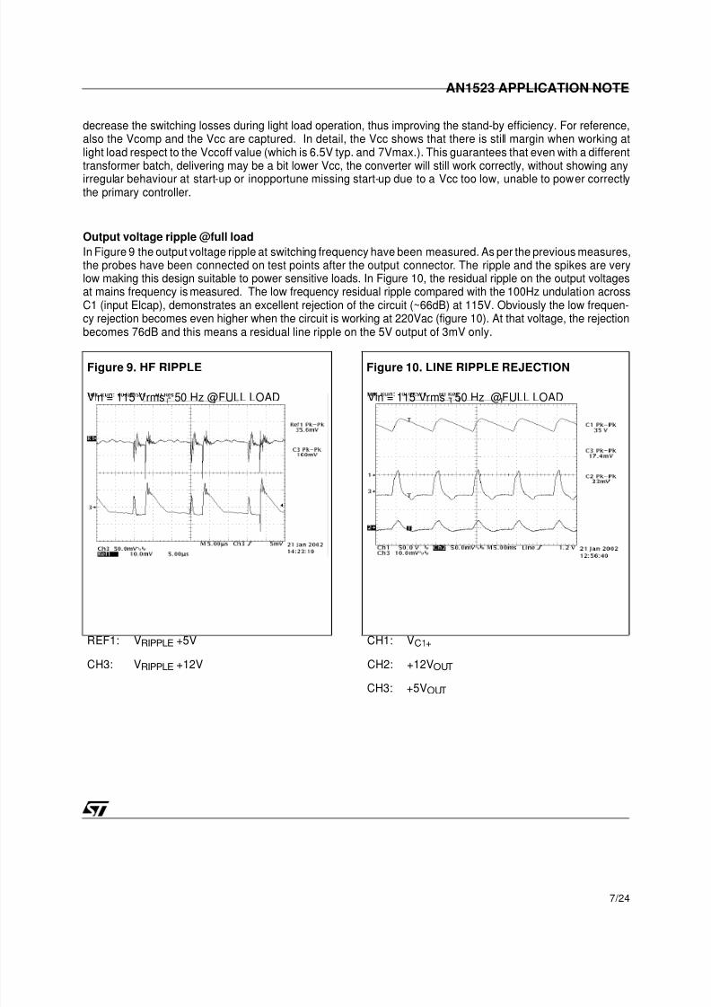
Output voltage ripple @full load
In Figure 9 the output voltage ripple at switching frequency have been measured. As per the previous measures,the probes have been connected on test points after the output connector. The ripple and the spikes are verylow making this design suitable to power sensitive loads. In Figure 10, the residual ripple on the output voltagesat mains frequency is measured. The low frequency residual ripple compared with the 100Hz undulation acrossC1 (input Elcap), demonstrates an excellent rejection of the circuit (~66dB) at 115V. Obviously the low frequen-cy rejection becomes even higher when the circuit is working at 220Vac (figure 10). At that voltage, the rejectionbecomes 76dB and this means a residual line ripple on the 5V output of 3mV only.
Figure 9. HF RIPPLE Figure 10. LINE RIPPLE REJECTION
Vin = 115 Vrms - 50 Hz @FULL LOAD Vin = 115 Vrms - 50 Hz @FULL LOAD
REF1: VRIPPLE +5V CH1: VC1+
CH3: VRIPPLE +12V CH2: +12VOUT
CH3: +5VOUT

8/8/2019 11w Flyback Converter_l6590
http://slidepdf.com/reader/full/11w-flyback-converterl6590 8/24
O b s o l e t e
P r o d u c
t ( s ) - O b s
o l e t e
P r o d u c
t ( s )
AN1523 APPLICATION NOTE
8/24
Dynamic Load Tests
The pictures 11 and 12 show the output voltage regulation against a dynamic load variation of +5V output, atthe nominal mains voltage values. As shown in the pictures, the voltage variation is always better than 1% andthe response is fast, within 2 ms. This allows to power µP or any logic circuitry without the risk of inopportunereset or logic malfunctioning. Even the 12V variation is good, remaining within its tolerance with still margin.
Start-Up Behaviours @full load
In figure 13 and 14 there are the rising slopes at full load of the output voltages at nominal input mains voltages.
As shown in the pictures, the rising time at 220Vac is a bit faster than at 115Vac, however they are similar. Therising slopes are always monotonic overall the input mains range. This characteristic is quite important power-ing a µP and its peripherals as in this case, thus avoiding problem at start-up for the equipment.
In figure 15, there are the same waveforms captured during the start-up in stand-by. Even in this case, the be-haviour of the circuit is always correct overall the input mains range.
A slight overshoot is present in all conditions but it is negligible because the voltage remains always under con-trol and the variation is within the tolerances.
Load condition: +12V: FULL LOAD
+5V: LOAD 50% ÷ 100%, 12Hz
Figure 11. DYNAMIC LOAD TEST Figure 12. DYNAMIC LOAD TEST
Vin = 115 Vrms - 50 Hz @FULL LOAD Vin = 220 Vrms - 50 Hz @FULL LOAD
CH1: VC1+ CH1: VC1+
CH3: +5VOUT CH3: +5VOUT
CH4: +5IOUT CH4: +5IOUT

8/8/2019 11w Flyback Converter_l6590
http://slidepdf.com/reader/full/11w-flyback-converterl6590 9/24
O b s o l e t e
P r o d u c
t ( s ) - O b s
o l e t e
P r o d u c
t ( s )
9/24
AN1523 APPLICATION NOTE
Figure 13. START-UP BEHAVIOUR Figure 14. START-UP BEHAVIOUR
Vin = 115 Vrms - 50 Hz @FULL LOAD Vin = 220 Vrms - 50 Hz @FULL LOAD
CH3: +5VOUT CH3: +5VOUT
CH4: +12VOUT CH4: +12VOUT
Wake-up time
In the following picture (Figure 16), there are thewaveforms with the wake-up time measured at 115V
input mains. Thanks to the L6590 internal currentsource, the capacitor C2 is charged with a constantcurrent, independent from the input mains value. Thismeans that the power supply wake-up time is perfect-ly constant. Thus, the annoying problem of a verylong start-up time, especially at low mains, is solvedwithout adding any additional extra component. Be-sides, it is a key feature during stand-by operation be-cause it is disconnected from the mains helping a lotthe power consumption decreasing.
The measured time in Figure 16 at 115Vac is lessthan 150ms but it doesn't show variations from 88 to265 Vac.
The traces shown in Figure 16 are the drain voltage,the Vcc and the +5V output: on the picture is clearlyvisible that no overshoots, undershoots, dips or anylost of control happens during the power supply start-up phase and the circuit starts correctly overall the in-put mains range
Figure 15. START-UP BEHAVIOUR
Vin = 115 Vrms - 50 Hz @STAND-BY
CH3: +5VOUT
CH4: +12VOUT

8/8/2019 11w Flyback Converter_l6590
http://slidepdf.com/reader/full/11w-flyback-converterl6590 10/24
O b s o l e t e
P r o d u c
t ( s ) - O b s
o l e t e
P r o d u c
t ( s )
AN1523 APPLICATION NOTE
10/24
Turn-Off
Even at turn off the transition is clean, without any ab-normal behaviour like overshoots or glitches both onthe output voltages. Checking the full load condition,a restart attempt is present on the Vcc voltage: it isdue to the circuit Q1, Q2,R9, R10, R11, C6 connect-ed to the COMP pin. During the switching off phasethe energy in the bulk capacitor is no more refreshed,then the voltage on it starts to decrease. This pro-vides for an increasing of the COMP pin voltage dueto the loop intervention which is regulating the outputvoltage while the input voltage is decreasing. At acertain value the COMP voltage is able to switch onQ1 and then Q2, thus disconnecting the transformerfrom Vcc, so that the L6590 stops the operation. Be-cause the circuit is switched off externally, the bulkcapacitor has still some energy stored and when the
Vcc has dropped below the Vccoff the IC detects thatresidual input voltage higher than its Drain start volt-age (Vdsmin). Hence the L6590 reactivates the inter-nal current source like in a normal start-up, and thevoltage on the Vcc pin tends to increase again. Butchecking the Fig. 17 it is important to note that theVcc value is far from the Start Threshold voltage (Vc-con), then no any perturbation appears on the output,avoiding any problem..
Figure 16. WAKE UP TIME
Vin = 115 Vrms - 50 Hz @FULL LOAD
CH1: VPIN1 - DRAIN VOLTAGE
CH2: VPIN3 - Vcc
CH3: +5VOUT
Figure 17. TURN-OFF Figure 18. TURN-OFF
Vin = 115 Vrms - 50 Hz @FULL LOAD Vin = 115 Vrms - 50 Hz @STAND-BY
CH1: VPIN1 – DRAIN VOLTAGE CH1: VPIN1 – DRAIN VOLTAGE
CH2: VPIN3 - Vcc CH2: VPIN3 - Vcc
CH3: +5VOUT CH3: +5VOUT

8/8/2019 11w Flyback Converter_l6590
http://slidepdf.com/reader/full/11w-flyback-converterl6590 11/24
O b s o l e t e
P r o d u c
t ( s ) - O b s
o l e t e
P r o d u c
t ( s )
11/24
AN1523 APPLICATION NOTE
Short-Circuit Tests @ Full Load
The short circuit tests have been done in two phases, making the test shorting by a power switch the outputelectrolytic capacitor or making the short by the active load option. This gives an idea about the circuit behaviourwith a hard short (at very low impedance) or with a "soft" short that could happen on the STB main board, havingslightly higher impedance. All the tests have been done at maximum, nominal and minimum input voltage. Forall conditions the drain voltage is always below the BVDSS, while the mean value of the output current has avalue close to the nominal one, thus preventing component melting for excessive dissipation in case of long termshorts. The auto-restart is correct at short removal in all conditions.
Figure 19. SHORT ON +5V Figure 20. SHORT ON +5V
Vin = 88 Vrms - 50 Hz @FULL LOAD Vin = 265 Vrms - 50 Hz @FULL LOAD
CH1: VPIN1 – DRAIN VOLTAGE CH1: VPIN1 – DRAIN VOLTAGE
CH2: VPIN3 - Vcc CH2: VPIN3 - Vcc
CH4: ISHORT CIRCUIT CH4: ISHORT CIRCUIT
Figure 21. SHORT ON +12V Figure 22. SHORT ON +12V
Vin = 88 Vrms - 50 Hz @FULL LOAD Vin = 265 Vrms - 50 Hz @FULL LOAD
CH1: VPIN1 – DRAIN VOLTAGE CH1: VPIN1 – DRAIN VOLTAGE
CH2: VPIN3 - Vcc CH2: VPIN3 - Vcc
CH4: ISHORT CIRCUIT CH4: ISHORT CIRCUIT

8/8/2019 11w Flyback Converter_l6590
http://slidepdf.com/reader/full/11w-flyback-converterl6590 12/24
O b s o l e t e
P r o d u c
t ( s ) - O b s
o l e t e
P r o d u c
t ( s )
AN1523 APPLICATION NOTE
12/24
As clearly indicated by the waveforms, the circuit starts to work in hiccup mode, keeping the current mean valueof the shorted output at levels within component rating. Because the working time and the dead time are im-posed by the charging and discharging time of the auxiliary capacitor C2, it is almost constant varying the inputmains voltage thanks to the internal start-up current source already mentioned.
Short-Circuit Tests @ Stand-by
A short circuit when the SMPS works at light-load is always a critical fault condition for any power supply circuit.In this condition, the energy deliverable to the short is the maximum one, and then it is the most stressing situ-ation for the output rectifiers and besides, sometimes the primary hiccup mode is not triggered. This may hap-pen because the short circuit reflected impedance on the auxiliary winding it is not low enough for decreasingthe Vcc voltage below the under-voltage lockout threshold or spikes are present at turn off on the auxiliary wind-ing which are capable of powering the IC. The proposed circuit, even in this load condition, provides the sameresults as the previous tests, both at 115Vac and at 220 Vac, making it reliable in all the working situationsindependently from the transformer coupling.
Figure 23. SHORT ON +5V Figure 24. SHORT ON +5V
Vin = 88 Vrms - 50 Hz @STAND-BY Vin = 265 Vrms - 50 Hz @STAND-BY
CH1: VPIN1 – DRAIN VOLTAGE CH1: VPIN1 – DRAIN VOLTAGE
CH2: VPIN3 - Vcc CH2: VPIN3 - Vcc
CH4: ISHORT CIRCUIT CH4: ISHORT CIRCUIT

8/8/2019 11w Flyback Converter_l6590
http://slidepdf.com/reader/full/11w-flyback-converterl6590 13/24
O b s o l e t e
P r o d u c
t ( s ) - O b s
o l e t e
P r o d u c
t ( s )
13/24
AN1523 APPLICATION NOTE
Short circuit of the output rectifiers
Another frequent problem in a power supply is rele-vant to the protection of the SMPS itself: thus some-times it is easy to find circuits with a good protectioncapability against shorts of the load but which are notable to survive in case of a very hard short like an out-put electrolytic capacitor or a diode. Besides, in caseof a rectifier shorted, the equivalent circuit of the ba-sic converter changes: in fact, due to the missing(shorted) rectifier the energy stored is delivered evenduring the on time, like in forward mode with reversepolarity of the trafo. To insure reliable operation ofthe circuit, even this fault condition has been simulat-ed (figure 25) shorting each rectifier, then has beenproven that the circuit can withstand this failure with-out any performance degradation. The circuit in factworks in hic-cup mode and then it restarts correctly to
deliver the output voltages if the short is removed.This exceeds the requirements of the VDE and IECsafety rules, and ensures a considerable time savingduring the qualification phase of the SMPS, avoidingfailures during the qualification tests, retrofit and newtesting, sometimes with a short time available tosolve the issue.
Figure 25. SHORT ON +5V RECTIFIER
Vin = 220 Vrms - 50 Hz @FULL LOAD
CH1: VPIN1 - DRAIN VOLTAGE
CH2: VPIN3 - Vcc
Switch On and Turn Off In Short Circuit Condition
The following pictures show the SMPS behaviour during the start-up phase with an output voltage shorted. Asclearly visible the circuit starts correctly then it works in hiccup mode protecting itself. The start-up phase isclean in all conditions, without showing any dangerous transition for the SMPS circuitry.
Figure 26. SWITCH ON WITH +5V SHORTED Figure 27. SWITCH ON WITH +5V SHORTED
Vin = 88 Vrms - 50 Hz @FULL LOAD Vin = 265 Vrms - 50 Hz @STAND-BY
CH1: VPIN1 – DRAIN VOLTAGE CH1: VPIN1 – DRAIN VOLTAGE
CH2: VPIN3 - Vcc CH2: VPIN3 - Vcc
CH3: +5Vout CH3: +5Vout

8/8/2019 11w Flyback Converter_l6590
http://slidepdf.com/reader/full/11w-flyback-converterl6590 14/24
O b s o l e t e
P r o d u c
t ( s ) - O b s
o l e t e
P r o d u c
t ( s )
AN1523 APPLICATION NOTE
14/24
Even at turn off in short circuit the SMPS functioning is good, protecting properly the circuit. No any abnormaltransition or level has been observed during the tests, confirming the design robustness proven so far.
Over Voltage Protection
A dangerous fault that could happen is the failure of the feedback circuitry. If this occurs, the SMPS output volt-ages can get to very high values, depending on the load on each output and on the transformer coupling be-tween the windings. Consequently, the rectifiers and the output capacitors are overstressed or damaged. A
possible solution could be to oversize the components but this should be expensive and uneconomic. Hence,to avoid this SMPS failure a suitable protection circuit has been added inside the L6590 and it doesn't requireany external component for the threshold setting. Hence, this fail has been simulated opening the feedbackloop and the circuit has been tested, giving the results shown in figures 30 and 31:
Figure 28. TURN-OFF WITH +5V SHORTED Figure 29. TURN-OFF WITH +5V SHORTED
Vin = 88 Vrms - 50 Hz @FULL LOAD Vin = 265 Vrms - 50 Hz @STAND-BY
CH1: VPIN1 – DRAIN VOLTAGE CH1: VPIN1 – DRAIN VOLTAGE
CH2: VPIN3 - Vcc CH2: VPIN3 - Vcc
CH3: +5Vout CH3: +5Vout
Figure 30. OPEN LOOP Figure 31. OPEN LOOP
Vin = 88 Vrms - 50 Hz @FULL LOAD Vin = 265 Vrms - 50 Hz @FULL LOAD
CH1: VPIN1 – DRAIN VOLTAGE CH1: VPIN1 – DRAIN VOLTAGE
CH2: VPIN3 - Vcc CH2: VPIN3 - Vcc
CH3: +5Vout CH3: +5Vout

8/8/2019 11w Flyback Converter_l6590
http://slidepdf.com/reader/full/11w-flyback-converterl6590 15/24
O b s o l e t e
P r o d u c
t ( s ) - O b s
o l e t e
P r o d u c
t ( s )
15/24
AN1523 APPLICATION NOTE
The figure 32 has been acquired testing the openloop protection when working in stand-by: as visible,even in this condition the circuit stops the switchingcycles when the Vcc reaches 16.5V and the value of
the output voltages never overstress the output elec-trolytic capacitors.
In case a lower OVP threshold is required, it is possi-ble to connect the inverting input of the E/A (VFB-pin5) to ground via a resistor (e.g. 1KΩ) and a zener be-tween the pin 5 and Vcc. A small ceramic capacitor inparallel to the resistor could be required. In this casethe OVP threshold will be VZENER + 2.5V.
Figure 32. OPEN LOOP
Vin = 220 Vrms - 50 Hz @STAND-BY
CH1: VPIN1 - DRAIN VOLTAGE
CH2: VPIN3 - Vcc
CH3: +5VOUT
CH4: +12VOUT
Conducted Noise Measurements (Pre-Compliance Test)
The following pictures are shown the quasi-peak conducted noise measurements at full load and standby withboth nominal input mains voltages. The limits shown on the diagrams are referred to the EN55022 CLASS B,which is the most widely used for domestic equipment like a TV or a STB. As visible on the diagrams, there is
a good margin of the measures with respect to the limits in overall conditions.
Figure 33. QUASI-PEAK MEASURE Figure 34. QUASI-PEAK MEASURE
Vin = 115 Vrms - 50 Hz @FULL LOAD
Limits: EN55022 CLASS B
Vin = 220 Vrms - 50 Hz @ FULL LOAD
Limits: EN55022 CLASS B

8/8/2019 11w Flyback Converter_l6590
http://slidepdf.com/reader/full/11w-flyback-converterl6590 16/24
O b s o l e t e
P r o d u c
t ( s ) - O b s
o l e t e
P r o d u c
t ( s )
AN1523 APPLICATION NOTE
16/24
Thermal measures
In order to check the reliability of the design, a thermal mapping by means of an IR Camera has been done.Here below the thermal measures on the board at both nominal input mains voltage at ambient temperature(25°C) are shown. The pointers A÷D have been placed across some key components affecting the reliability ofthe circuit. The points correspond to the following components:
As shown on the maps, all the other points of the board are within the temperature limits ensuring a reliableperformance of the devices. TAMB = 25°C for all measures
Figure 35. QUASI-PEAK MEASURE Figure 36. QUASI-PEAK MEASURE
Vin = 115 Vrms - 50 Hz @STAND-BY
Limits: EN55022 CLASS B
Vin = 220 Vrms - 50 Hz @STAND-BY
Limits: EN55022 CLASS B
TESTED POINT NOTES
A IC1 - L6590 Copper dissipating area: 4 cm2
B D1 - BZW06–188Lead length: 13mm each side – Diode mounted 7mm from thetop of PCB surface
C T1 - TRAFO Checked the hottest point
D D4 – BYW98-200Lead length: 8 mm each side – Diode body placed on PCBsurface
Figure 37. TEMPERATURE IR MEASURE Figure 38. TEMPERATURE IR MEASURE
Vin = 115 Vrms - 50 Hz @FULL LOAD Vin = 220 Vrms - 50 Hz @FULL LOAD

8/8/2019 11w Flyback Converter_l6590
http://slidepdf.com/reader/full/11w-flyback-converterl6590 17/24
O b s o l e t e
P r o d u c
t ( s ) - O b s
o l e t e
P r o d u c
t ( s )
17/24
AN1523 APPLICATION NOTE
Conclusions
A SMPS for Consumer application has been completely designed and tested, checking the performance thor-oughly. The test results has been positive and the initial requirements of high reliability, low cost and low com-plexity have been met successfully.
References
[1] AN1261 - Getting familiar with the L6590 family high-voltage fully integrated power supply
[2] AN1262 - Offline fly-back converters design methodology with the L6590 family
ANNEX1: Part List
Designator Part Type Description Supplier
1 C1 22uF-400V ELCAP ELNA
2 C10 330PF CERCAP AVX
3 C11 470uF-25V YXF ELCAP RUBYCON
4 C2 22uF-25V ELCAP ELNA
5 C3 2N2 CERCAP AVX
6 C4 2N2-2KV (Y1) CERCAP-SAFETY CERA-MITE
7 C5 100N-250Vac - B81133 X CAP-MKT EPCOS
8 C6 2u2-50V - YK ELCAP RUBYCON
9 C7 1000uF-25V YXF ELCAP RUBYCON
10 C8 220uF-10V-ZL ELCAP RUBYCON
11 C9 100NF CERCAP AVX
12 D1 BZW06-188 AXIAL TRANSIL DIODE STMicroelectronics
13 D2 STTA106 ULTRA FAST REC. RECTIFIER STMicroelectronics
14 D3 1N4148 GEN. PURPOSE DIODE WISHAY
15 D4 BYW98-200 FAST REC. RECTIFIER STMicroelectronics
16 D5 BYW100-200 FAST REC. RECTIFIER STMicroelectronics
17 D6 DF04G BRIDGE RECTIFIER GEN. SEMICOND.
18 F1 FUSE1 T2A - 250V19 IC1 L6590_MINIDIP INTEGRATED CONTROLLER STMicroelectronics
20 IC2 TL431ACZ SHUNT REGULATOR STMicroelectronics
21 L1 B82731-R2501-A30 2*27mH FILTER COIL EPCOS
22 L2 4.7uH ELC08D INDUCTOR PANASONIC
23 OPT1 PC817 OPTOCOUPLER SHARP
24 Q1 BC548 SMALL SIGNAL BJT ZETEX
25 Q2 BC548 SMALL SIGNAL BJT ZETEX
26 R1 12R - 1/4W - 5% SFR25 BEYSCHLAG
27 R10 33K - 1/4W - 5% SFR25 BEYSCHLAG
28 R11 10K - 1/4W - 5% SFR25 BEYSCHLAG
29 R12 NTC_10R S236 NTC THERMISTOR EPCOS
30 R13 4K7 - 1/4W - 5% SFR25 BEYSCHLAG
31 R2 6K8 - 1/4W - 5% SFR25 BEYSCHLAG
32 R3 560R - 1/4W - 5% SFR25 BEYSCHLAG
33 R4 2K4 - 1/4W - 1% MBA0204 BEYSCHLAG
34 R5 1K0 - 1/4W - 5% SFR25 BEYSCHLAG
35 R6 2K4 - 1/4W - 1% MBA0204 BEYSCHLAG
36 R7 560R - 1/4W - 5% SFR25 BEYSCHLAG
37 R8 2K7 - 1/4W - 5% SFR25 BEYSCHLAG
38 R9 1K0 - 1/4W - 5% SFR25 BEYSCHLAG
39 T1 2362.0019 rev. C POWER TRANSFORMER ELDOR CORPORATION
40 PCB - SINGLE SIDE - 70um - 100x50 mm
8/8/2019 11w Flyback Converter_l6590
http://slidepdf.com/reader/full/11w-flyback-converterl6590 18/24
O b s o l e t e
P r o d u c
t ( s ) - O b s
o l e t e
P r o d u c
t ( s )
AN1523 APPLICATION NOTE
18/24
ANNEX 2 - Switch Mode Transformer Specification
EVOLUZIONE DELLE REVISIONI / revision evolution: DOCUMENTO N / document Nbr:
REV
rev
DATA
date
EMESSO DA:
issued by:
VERIFICATO DA:
checked by:
APPROVATO DA:
approved by:
PAGINEMODIFICATE:
changedpages:
DESCRIZIONE MODIFICA:
change description:
A 12/02/02 GL. Verga
SWITCH MODE TRANSFORMER SPECIFICATION
CODE : 2362.0019 C
FIRST ISSUE DATE : 12/02/2002
Table of contents:
1.0 GENERAL INFORMATION
2.0 ELECTRICAL CHARACTERISTICS
3.0 SAFETY
4.0 MATERIAL LIST
5.0 MECHANICAL CHARACTERISTICS
COPIA ASSEGNATA A:Copy assigned to:
ELDOR CORPORATION S.p.A.Via Plinio, 1022030 ORSENIGO - Como - ItalyTel. +39 031 636111 - Telefax +39 031 636263

8/8/2019 11w Flyback Converter_l6590
http://slidepdf.com/reader/full/11w-flyback-converterl6590 19/24
O b s o l e t e
P r o d u c
t ( s ) - O b s
o l e t e
P r o d u c
t ( s )
19/24
AN1523 APPLICATION NOTE
ANNEX 2 - Switch Mode Transformer Specification (continued)
SWITCH MODE TRANSFORMER SPECIFICATION 2362.0019 C
CUSTOMER CODE ISSUE A
This document and its content are property of ELDOR CORPORATION S.p.A. No part of this document may bereproduced, published, disclosed or used in any form with out written permission of ELDOR CORPORATION S.p.A. DOC.N. PAG. 2 / 6
1.0 GENERAL INFORMATION
1.1 Description
The magnetic circuit comprises two soft ferrite E-cores glued together and gapped on the central leg.The windings are placed concentrically on single plastic bobbin made in self extinguish material.The transformer comply with the standard (Refer to pharagraf “3.0 SAFETY”) for the component connected to themains because:the use of triple insulation wire (three different layers) for the secondary winding.the thickness of insulation that exceed 0.40 mm.the shape of coilformer that maintain the safety creeping distance from the core , that is consiredbelong the primary side, and the secondary output pins and the circuit components.Winding outputs are made through 8 pins placed in two parallel rows (Refer to page 6).
1.2 Application
The transformer is designed for use in a switch mode flyback power supply.
1.2.1 Operating conditions
Operating ambient temperature: 0˚C to +60˚C
Operating humidity range non condensing 10% to 85%RH
Ambient temperature is the medium value measured at 30 mm. of distance from the surface of the transformer.When the transformer is placed inside a metallic shield the above temperature value will be referred to the inside ofthe shield even if it is closer then 30 mm to the SMT.
1.3 Storage conditions
Storage temperature -20˚C to +50˚CAfter storage to allow a minimum of 24 hours recovery time before testing.
1.4 Marking
The component is marked with:- Eldor part number and customer part number ( if required).- Production date.
1.5 Packaging
TDB
1.6 Weight
The transformer weight is approx 15g.

8/8/2019 11w Flyback Converter_l6590
http://slidepdf.com/reader/full/11w-flyback-converterl6590 20/24
O b s o l e t e
P r o d u c
t ( s ) - O b s
o l e t e
P r o d u c
t ( s )
AN1523 APPLICATION NOTE
20/24
ANNEX 2 - Switch Mode Transformer Specification (continued)
SWITCH MODE TRANSFORMER SPECIFICATION 2362.0019 C
CUSTOMER CODE ISSUE A
This document and its content are property of ELDOR CORPORATION S.p.A. No part of this document may bereproduced, published, disclosed or used in any form with out written permission of ELDOR CORPORATION S.p.A. DOC.N. PAG. 3 / 6
2.0 ELECTRICAL CHARACTERISTICS
For pins identification refer to mechanical drawing
2.1 Static characteristics
2.1.1 Inductance and DC resistance:
Measurement of inductance is made using a LCR bridge at frequency of 10KHz at output voltage of 1 V r.m.s.Measurement of resistance is made using a four wire ohmmeter.Temperature should be 23 ± 2˚C.
L(mH) tol(%) R(Ω) tol(%)
Between pin 2 and pin 1 2.0 ±10 2.31 ±15
2.1.2 Leakage Inductance:
LL= 6 %Lp (pin 2 pin 1 )
Measurement is made with the secondary windings short circuited.Measurement if inductance is made using a LCR bridge at frequency of 10 kHz and at output voltage of 1 V R.M.S.
2.1.3 Withstanding voltage
The transformer shall withstand a voltage of 3.75kV RMS for 60 seconds between primary winding and secondarywindings.The frequency of the test voltage shall be 50 or 60Hz.
2.2 Test circuit diagram and application conditions
+5V/1.4A
+12V/0.3A1
4
5
7
6
8
2
3
+V
Drain
supply IC

8/8/2019 11w Flyback Converter_l6590
http://slidepdf.com/reader/full/11w-flyback-converterl6590 21/24
O b s o l e t e
P r o d u c
t ( s ) - O b s
o l e t e
P r o d u c
t ( s )
21/24
AN1523 APPLICATION NOTE
ANNEX 2 - Switch Mode Transformer Specification (continued)
SWITCH MODE TRANSFORMER SPECIFICATION 2362.0019 C
CUSTOMER CODE ISSUE A
This document and its content are property of ELDOR CORPORATION S.p.A. No part of this document may bereproduced, published, disclosed or used in any form with out written permission of ELDOR CORPORATION S.p.A. DOC.N. PAG. 4 / 6
2.3 Temperatures
2.3.1 Temperature raise of the primary coil The raising in primary winding shall be made in the following condition: Vin nom. and all loads at maximum current,except that for the Audio output that must be adjusted at 50% Imax.Raise of temperature after 4 hours must be lower than 55˚C
2.3.2 Maximum allowable temperatures
In the application, TV set with cabinet closed, at the maximum allowable ambient temperature (See IEC68-1 clause4.6.2) and at the maximum working conditions (see § 2.3.1) after 4 hours the temperature of the transformer mustbe = 115˚C.To satisfy the above conditions it is raccomanded to provide the SMT with sufficient cool air flow around it.
2.4 Core saturation
Test must be performed in the following way:a) The SMT must be placed in oven at ambient temperature of 100 C for 2 hours.b) Using the circuit as per figure, connect the primary winding to LCR meter operating at frequency of 1
kHz and output voltage of 1 V.c) Superimpose through the power supply a dc current and read on the LCR meter the correspondent
value of the inductance. Do this up to a current value of I peak max input current.d) The value of the inductance must not shows saturation (0.7Lp).
A
CHOKE
(1H or more)SPECIMEN
C (40000 µF or more)
LCR
METER
+
Saturation current @100˚C
0,50
0,60
0,70
0,80
0,90
1,00
1,10
0 0,15 0,3 0,45 0,6 0,75 0,9
I (A)
L x / L p

8/8/2019 11w Flyback Converter_l6590
http://slidepdf.com/reader/full/11w-flyback-converterl6590 22/24
O b s o l e t e
P r o d u c
t ( s ) - O b s
o l e t e
P r o d u c
t ( s )
AN1523 APPLICATION NOTE
22/24
ANNEX 2 - Switch Mode Transformer Specification (continued)
SWITCH MODE TRANSFORMER SPECIFICATION 2362.0019 C
CUSTOMER CODE ISSUE A
This document and its content are property of ELDOR CORPORATION S.p.A. No part of this document may bereproduced, published, disclosed or used in any form with out written permission of ELDOR CORPORATION S.p.A. DOC.N. PAG. 5 / 6
3.0 SAFETY
According to international standard EN60065- EN60950 for the Class II at the following conditions ofprimary voltage: VRMS <300V; Vp<600VAll the transformers are tested at the end of the manufacturing lines for the withstanding voltage in betweenprimary and secondary in the following conditions:Test voltage = 4.2 kV RMSDuration of test = 1 secondsFile records of the test are mantained in Eldor Quality Assurance Dept.
4.0 MATERIAL LIST
NR. SMT PART NAME KIND OF MATERIAL MANUFACTURER TRADE MARK/TYPEUL
RATINGUL FILE
NUMBER
1 BOBBIN Polyamide 4/6 (PA4/6) DSM Stanyl TE250F6 94V-0 E119177
2 INSULATING TAPE Polyester film 3M 1350 UL 130˚C E17385
3 TERMINAL PINS Tinned steel
4 FERRITE CORE N67 or equivalent
Epcos AG, AVX,Samwha, Ferroxcube,ISU, DMEG,Tridelta orequivalent
E20/10/6
5 PRIMARY WINDINGSEnamelled wireGrade 2 - Class F
Elektrisola Atesina srl,NexansPirelli cavi e sistemior equivalent
6SECONDARYWINDINGS
Triple insulated wire The Furukawa Electric TEX-E E206440
7 ADHESIVE LOCTITE Loctite 480
8 ELASTIC ADHESIVE 3M Scotch Grip EC -1022
9 MARKING OR LABEL Mark ing
1
5
6
4
2
7
8
8/8/2019 11w Flyback Converter_l6590
http://slidepdf.com/reader/full/11w-flyback-converterl6590 23/24
O b s o l e t e
P r o d u c
t ( s ) - O b s
o l e t e
P r o d u c
t ( s )
23/24
AN1523 APPLICATION NOTE
ANNEX 2 - Switch Mode Transformer Specification (continued)
SWITCH MODE TRANSFORMER SPECIFICATION 2362.0019 C
CUSTOMER CODE ISSUE A
This document and its content are property of ELDOR CORPORATION S.p.A. No part of this document may bereproduced, published, disclosed or used in any form with out written permission of ELDOR CORPORATION S.p.A. DOC.N. PAG. 6 / 6
ALL DIMENSIONS IN mm
GENERAL TOLERANCE ± 0.2
5.0 MECHANICAL DRAWINGS
HOLES PATTERNComponent Side
REFERENCE MARK FOR PINS IDENTIFICATION
=
=
==
= == =
= =
= =
7
. 5
±
0 .
1
5
±
0 . 1
16.25 ±0.1
7.5±0.1 5 ±0.1
17.5
20+0.8-0.6
5 .
9
0
- 0 .
5
1±0.1ø
16.25 ± 0.1
1 9
±
0 .
1
4 .
5
±
0 .
5
6.8 9.45
57.5
17.5
1.3+0.10N˚ 8 ho les ø
±0.1±0.1
=
=
1 4 .
1 + 0 .
8
0
25.5 ±0.1
2 2 .
4
±
0 .
1 =
=
4
3
2
1
5
6
7
8
1
1
4
8
5

8/8/2019 11w Flyback Converter_l6590
http://slidepdf.com/reader/full/11w-flyback-converterl6590 24/24
O b s o l e t e
P r o d u c
t ( s ) - O b s
o l e t e
P r o d u c
t ( s )
Information furnished is believed to be accurate and reliable. However, STMicroelectronics assumes no responsibility for the consequencesof use of such information nor for any in fringement of patents or other rights of third parties which may result from its use. No license is grantedby implication or otherwise under any patent or patent rights of STMicroelectronics. Specifications mentioned in this publication are subjectto change without notice. This publication supersedes and replaces all information previously supplied. STMicroelectronics products are notauthorized for use as critical components in life support devices or systems without express written approval of STMicroelectronics.
The ST logo is a registered trademark of STMicroelectronics® 2002 STMicroelectronics - All Rights Reserved
STMicroelectronics GROUP OF COMPANIESAustralia - Brazil - Canada - China - Finland - France - Germany - Hong Kong - India - Israel - Italy - Japan -Malaysia - Malta - Morocco -
Singapore - Spain - Sweden - Switzerland - United Kingdom - United States.http://www.st.com
24/24
AN1523 APPLICATION NOTE