design and power dissipation consideration of pfal cmos v
TRANSCRIPT

Design and Power Dissipation Consideration ofPFAL CMOS v/s Conventional CMOS based 2:1Multiplexer and Full AdderManvinder Sharma
Chandigarh Group of CollegesDigvijay Pandey ( [email protected] )
DTE https://orcid.org/0000-0003-0353-174XPankaj Palta
Chandigarh Group of CollegesBinay Kumar Pandey
Govind Ballabh Pant University of Agriculture and Technology: Govind Ballabh Pant University ofAgriculture & Technology
Research Article
Keywords: Low Power Design, Adiabatic, PFAL, Multiplexer, Adder
Posted Date: April 29th, 2021
DOI: https://doi.org/10.21203/rs.3.rs-427022/v1
License: This work is licensed under a Creative Commons Attribution 4.0 International License. Read Full License

Design and Power Dissipation Consideration of PFAL
CMOS v/s Conventional CMOS based 2:1
Multiplexer and Full Adder
Manvinder Sharma1, Digvijay Pandey2, Pankaj Palta3 and Binay Kumar Pandey4
1,3Department of ECE, Chandigarh Group of Colleges, Landran, Punjab India 2Department of Technical Education, IET, Dr. A.P.J. Abdul Kalam Technical University, Uttar
Pradesh,India 4Departmentt of IT,College of Technology, GovindBallabh Pant University of Agriculture and Technology,
U.K, India
e-mail: [email protected],[email protected]
Abstract—Increasing transistor switching time and rising count of transistors integrated over a chip area has
given a high pace in computing systems by several orders of magnitude. With the integration of circuits,
number of gates and transistors are increasing per chip area. CMOS Logic family is preferred due to its
performance and impeccable noise margins over other families. However with integration in every digital
circuit, the energy due to switching of gate doesn’t decrease at same rate as gates are increased per chip area.
Due to this, power dissipation becomes significant and also reduction of heat becomes more complicated
and expensive. In CMOS based circuits dynamic power requirement is becoming major concern in digital
circuits. In this paper, the work is focused on reducing the power dissipation in circuits which is increasing
with down scaling of circuits. The work is done on 2:1 multiplexer and full adder circuit. Adiabatic logic
with positive feedback (PFAL) is applied to redesign the circuit with input power taken as sinusoidal source
of 3.3 V and analysis is done for power dissipation between conventional CMOS and PFAL based CMOS
circuits. In comparison with the conventional CMOS 2:1 multiplexer circuit, the designed PFAL CMOS 2:1
multiplexer circuit has less power dissipation as 80.871 picoWatts while conventional CMOS circuit has
6.9090 nanoWatts with the same behavior of circuit. Also for full adder conventional CMOS circuit have
48.0452 picoWatts while PFAL based full adder has 3.9089 picoWatts.
Keywords-Low Power Design; Adiabatic; PFAL; Multiplexer; Adder
I. INTRODUCTION
For high speed performance in computingand other applications which involve processing, computing and
analysis of any signal, digital CMOS circuits have been used mostly. Several pros over other families which
include perfect logic levels, impeccable noise margins, better performance and almost negligible static power
dissipation CMOS logic family is preferred. As we need faster processing of signals, the demand of these
circuits is high and is going to increase in near future. Faster speed in computing is achieved with the increase
in number of transistors integrated over a chip. However such improvement in performance is accompanied
with increase in energy dissipation and power dissipation [1]. The disadvantage of higher energy and power
dissipation is that the circuits require more expensive packaging and expansive cooling technology which
decreases reliability also increases cost. As the level of clock frequency and on-chip integration will continue
to grow as per the demands of faster computing, the energy and power dissipation of these high performance
circuits is a perilous design issue [2]. To achieve Tera Instructions per seconds (TIPS) high end

microprocessor employ billions of transistor on chip at clock rates over 30 GHz, with this rate of speed power
dissipation of circuit is projected to extend to thousands of watts. Such power dissipation density introduces
reliability concerns like hot carrier, thermal stress and electromigration which degrade the performance of
circuits. Also for the requirement of low power chips or low battery consuming chips the higher power
dissipation circuits will consume more power from the battery [3-5]. For the portable digital systems that run
on batteries like notepads, laptops, tablets etc the prime concern is low power consumption and this also
increases the battery longevity.
The power consumed by any device is the energy consumed per unit time.
𝐸 = ∫ 𝑃(𝑡)𝑑𝑡𝑇𝑜𝑝0 (1)
For a given operation the energy (E) required is integral of power (P) consumed over operation time (Top)
The power of digital CMOS circuit is given by
P = C.VDD.Vs.f (2)
Where VDD is supply voltage, f is clock frequency, C is capacitance being recharged and Vs is voltage
swing of signal.
The energy consumption can be given by
E=n.C.VDD.VS (3)
In this equation energy consumption is independent of clock frequency. As the battery life is determined
by energy consumption it is imperative to reduce energy as compared with power. However power is critical
for heat dissipation considerations. So optimization of both factors energy as well as power is required [6].
In CMOS circuit, power dissipation is composed of static and dynamic power dissipation. Static power
dissipation is power dissipated in steady state and is given by
Pstst = Istat .VDD (4)
Where Istat is current when circuit is in steady state or in the absence of switching activity. However
theroticlly, in static state there is no direct path from VDD to ground (pMOS) and no transistor is on state
(nMOS) there is no static power dissipation [7]. But in practice Metal-Oxide-Semiconductor (MOS) is not a
perfect or impeccable switch due to this there is always a substrate injection current and leakage current
which introduces static power dissipation [8-10]. For 5 Volts of VDD, substrate injection current for a nMOS
device (W/L= 10/0.5) is in order to 1-100 µA [11].
Another subcategory of static power dissipation is ratioed logic. As CMOS family is ratioed family pull up
of pMOS is in always on state which also acts as load for pull down nMOS network. In low state, when gate
output is low there is direct path for current from VDD to ground. In this state static current flows. So in
CMOS family static power consumption is considerable. Figure 1 shows the CMOS Inverter operation.

Figure 1. CMOS Inverter for power analysis
Dynamic power dissipation is introduced in the circuit while switching activity, or in transition state.
During the transient activity, at a point which is Vtn (nMOS threshold point) and VDD-Vtp(pMOS threshold
point) both pMOS and nMOS are turned on. A short circuit exists in this duration and current has path from
VDD to ground. With the cautious designing of edges of transition this effect can be minimized to ten to
fifteen percent of power of total. The other factor affecting dynamic dissipation is due to charging of parasitic
capacitance and discharging of parasitic capacitance within the circuit [12]. In figure 1, the parasitic
capacitance is shown as a output as a capacitor. Considering one full cycle of operation from VDD to GND
and from GND to VDD, the process of charging the capacitor draws energy from the power supply which is
equal to C .(VDD )2. Half power is stored in capacitor while half is dissipated in pMOS, during operation
ground to VDD, the capacitance is discharged and energy is dissipated in nMOS. For each time the capacitance
switches, energy equals to C. (VDD)2 is dissipated. The dynamic dissipation can be formulated as
Pdyn= αCVDD2f (5)
Where, α is expected number of 0 to 1 transitions per data cycle, f is clock frequency.
II. PFAL MODELING DESIGN
The dissipation takes most of power dissipation almost 90%. To reduce this dissipation, designers can
decrease node capacitance, minimize switching events, reduce voltage swing or also can smear grouping of
these. But in all these methods before power dissipation, energy which is drawn from power supply is used
once. However, if we introduce recycling of energy drawn from power supply, the energy efficiency of logic
circuits can be achieved [10]. The possibility of reusing energy drawn from the supply and reducing the
energy dissipation during switching is offered by a class of circuits known as Adiabatic logic circuits. In this
logic, the energies stored in capacitance are reused instead of being dissipated as heat. This is also known and
energy recovery CMOS. By only switching the transistors under certain conditions and slowing switching
process one can achieve very low power dissipation in the circuit [11].

Figure 2. Adiabatic CMOS as Inverter
Figure 3. Equivalent resistive circuit of Inverter
Figure 4. Adiabatic switching
Figure 2,3,4 shows adiabatic switching process, Instead of constant voltage source [14], the capacitance is
charged by constant current source, R shows resistance of pMOS,
A constant charging current corresponds to linear voltage ramp.
Initially, let us assume capacitance voltage VC = 0
IR be the voltage across switch
P(t) in the switch = I2R (6)
Energy during charge = (I2R) T (7)
∴ 𝐼 = 𝐶𝑉𝑇 → 𝑇 = 𝐶𝑉𝐼 (8)

𝐸 = (𝐼2𝑅)𝑇 = (𝐶𝑉𝑇 )2 𝑅𝑇 = 𝐶2𝑉2𝑅𝑇 (9) 𝐸 = 𝐸𝑑𝑖𝑠𝑠 = (𝑅𝐶𝑇 ) 𝐶𝑉2 = (2𝑅𝐶𝑇 ) (12 𝐶𝑉2) (10)
E is energy dissipated, Q is charge transfer to load, C is load capacitance, R is Resistance of MOS Switch,
V is final value of voltage and T is time spent at load.
From equation 9, if the charging time (T) is greater than 2RC, the energy dissipation can be made small by
increasing charging time. Opposed to conventional CMOS, the dissipated energy is proportional to R instead
of capacitance and voltage swing. Reducing on resistance of pMOS will reduce energy dissipation.
To reuse the power a different type of power supply is used in the adiabatic logic. The source needed for
adiabatic operation is usually a sinusoidal or a trapezoidal source. This supply can also act as clock for circuit.
Figure 5 shows trapezoidal power supply. The four phases idle, evaluate, hold and recovery shows the
process. Idle is equal to 0 and hold is equal to 1. While in evaluate phase, depending upon input the load
capacitance charges up or does not and in recovery phase the charge held on capacitance is recovered.
Figure 5. Different phases in adiabatic power supply.
Positive feedback adiabatic logic (PFAL) is the category under adiabatic logic family. As compared to
other families like ECRL, 2N-2N2P, CAL this PFAL has lowest energy consumption [15]. It is robust against
technological parameter variations. The core of PFAL is adiabatic amplifier, latch made by two nMOS and
two pMOS. The two n-trees reliaze logic functions as well as it can generate both positive and negative
outputs which can be used as per requirement. Figure 6 shows general schematic of PFAL gate [16-17]. Two
latches M1 and M2 and M3 and M4 formed by pMOS andnMOS.
Figure 6.General schematic of PFAL gate.
In mentor graphic design architect IC conventional CMOS based 2:1 multiplexer is modeled and analyzed
for power dissipation which is shown in figure 7 and figure 8 shows conventional CMOS based full adder
which is modeled and analyzed.

Figure 7. Conventional CMOS based 2:1 Multiplexer
Figure 8. Conventional CMOS based Full Adder
Using the discussed methodology, PFAL based 2:1 multiplexer and full adder is designed and modeled in
mentor graphic design architect IC and is shown in figure 9 and figure 10 respectively. The designs are
simulated in ELDONET tool.
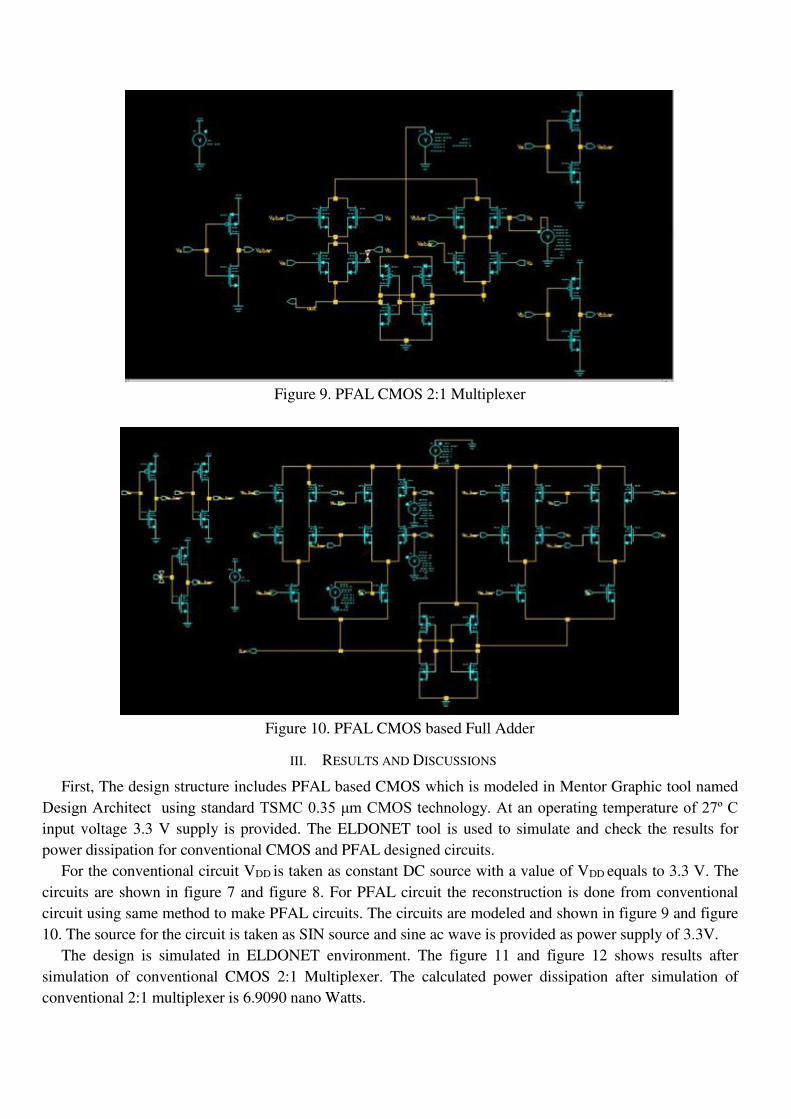
Figure 9. PFAL CMOS 2:1 Multiplexer
Figure 10. PFAL CMOS based Full Adder
III. RESULTS AND DISCUSSIONS
First, The design structure includes PFAL based CMOS which is modeled in Mentor Graphic tool named
Design Architect using standard TSMC 0.35 μm CMOS technology. At an operating temperature of 27º C input voltage 3.3 V supply is provided. The ELDONET tool is used to simulate and check the results for
power dissipation for conventional CMOS and PFAL designed circuits.
For the conventional circuit VDD is taken as constant DC source with a value of VDD equals to 3.3 V. The
circuits are shown in figure 7 and figure 8. For PFAL circuit the reconstruction is done from conventional
circuit using same method to make PFAL circuits. The circuits are modeled and shown in figure 9 and figure
10. The source for the circuit is taken as SIN source and sine ac wave is provided as power supply of 3.3V.
The design is simulated in ELDONET environment. The figure 11 and figure 12 shows results after
simulation of conventional CMOS 2:1 Multiplexer. The calculated power dissipation after simulation of
conventional 2:1 multiplexer is 6.9090 nano Watts.

Figure 11. Calculated power dissipation of Conventional CMOS based 2:1 Multiplexer
Figure 12. Log window of power dissipation of Conventional CMOS based 2:1 Multiplexer
PFAL 2:1 multiplexer is simulated and results as power dissipation is shown in figure 13 and figure 14.
The calculated power dissipation in this circuit is 80.8716 pico Watts. It can be observed that the power
dissipation is reduced with high rate with the same working of circuit. Figure 15 shows the comparison of
power dissipation for 2:1Multiplexer.

Figure 13. Calculated power dissipation of PFAL CMOS based 2:1 Multiplexer
Figure 14. Log window of power dissipation for PFAL based 2:1 Multiplexer

Figure 15. Graphical representation of reduction in power dissipation of 2:1 Multiplexer
The figure 16 and figure 17 shows results after simulation of conventional CMOS full adder. The
calculated power dissipation after simulation is 48.0452 picoWatts.
Figure 16. Calculated power dissipation of conventional CMOS based Full Adder
Figure 17. Log window of power dissipation of conventional CMOS based Full Adder
6.909
0.080871
0
1
2
3
4
5
6
7
8
2:1 Multiplexer Power
Dissipation
(Nano Watt)
Conventional
CMOS
PFAL CMOS

Figure 18. Calculated power dissipation of PFAL based Full Adder
PFAL CMOS based full adder is simulated and results as power dissipation is shown in figure 18 and
figure 19. The calculated power dissipation in this circuit is 3.9089 picoWatts. It can be observed that the
power dissipation is reduced with the same working of circuit. Figure 20 shows the comparison of power
dissipation for both full adder circuit.
Figure 19. Log window of power dissipation for PFAL based Full Adder.
Figure 20. Graphical representation of reduction in power dissipation of Full Adder Circuit
48.0452
3.9089
0
10
20
30
40
50
60
Full Adder Power Dissipation
Comparision
(Pico Watt)
Conventional
CMOS
PFAL CMOS

Table 1 shows the different circuit modeled and simulated in eldonet environment and their power
dissipation.
Table 1. Power dissipation of Conventional CMOS v/s PFAL CMOS
After the simulation of all circuits (convention CMOS 2:1 multiplexer, Conventional CMOS full adder,
PFAL CMOS 2:1 multiplexer and PFAL full adder) it can be clearly seen that the power dissipation of the
circuit using PFAL is reduced to a much lower value.. However the circuit for PFAL has increased the
number of gates required to perform any logic but it is also providing both original and its complement
outputs. This can eliminate the requirement of other circuit where complement of output is also required for
many applications
IV. CONCLUSION
While rate of integration of transistor per chip area is increasing day by day. This leads to power
dissipation and expansive heat cooling methods. The power dissipation directly affects the device
performance in reliability terms and performance of circuit. The focus is on reducing the power dissipation.
In this paper, another approach for reducing and reusing the power and energy dissipation is discussed. Using
PFAL method, 2:1 multiplexer circuit power dissipation is reduced to picoWatts from nanoWatts of
conventional CMOS circuit. For full adder the power dissipation is also reduced for PFAL circuitry. This
shows the effectiveness of PFAL and adiabatic logic family. The circuits can be made with this approach to
reduce the power dissipation. With the less power dissipation and consumption the hand held devices like
laptop, mobiles, notepads etc will have longevity of battery. Also the cost of expensive heat cooling will be
reduced
Acknowledgements
The authors would like to express gratitude to Department of Technical Education and Chandigarh Group of
Colleges, Landran, Punjab India. The authors would also like to thank to Vice Chancellor, Dr. A.P.J. Abdul
Kalam Technical University, and Uttar Pradesh, India
Code Availability
The relevant code with the manuscript is also available and would be available, if will be asked to do so later.
Funding statement: The author(s) received no financial support for the research, authorship, and/or
publication of this article.
Availability of Data and Material
Circuit Power Dissipation
(Watts)
Conventional CMOS 2:1 Multiplexer 6.9090 Nano
PFAL CMOS 2:1 Multiplexer 80.871 Pico
Conventional CMOS Full Adder 48.0452 Pico
PFAL CMOS Full Adder 3.9089 Pico

The data samples have been taken using PFAL.
Contributions
All authors approve the final manuscript.
Ethics declarations
Ethics Approval
Not Applicable (as the results of studies does not involve any human or animal).
Consent to Participate
Not Applicable (as the results of studies does not involve any human or animal).
Consent for Publication
Not Applicable (as the results of studies does not involve any human or animal).
Conflict of Interests/ Competing Interests
The authors declare that they have ‘no known conflict of interests or personal relationships’ that could have appeared to influence the work reported in this paper.
REFERENCES
[1] Samaali, Hatem, Y. Perrin, A. Galisultanov, H. Fanet, Gaël Pillonnet, and Philippe Basset. "MEMS four-terminal
variable capacitor for low power capacitive adiabatic logic with high logic state differentiation." Nano Energy 55
(2019): 277-287.
[2] Liu, Jheng-Sin, Michael B. Clavel, and Mantu K. Hudait. "TBAL: Tunnel FET-Based Adiabatic Logic for
Energy-Efficient, Ultra-Low Voltage IoT Applications." IEEE Journal of the Electron Devices Society 7 (2019):
210-218.
[3] Raghav, H. S., Bartlett, V. A., & Kale, I. (2018). Investigating the effectiveness of Without Charge-Sharing
Quasi-Adiabatic Logic for energy efficient and secure cryptographic implementations. Microelectronics journal,
76, 8-21.
[4] A. P. CHANDRAKASAN, S. SHENG, AND R. W. BRODERSEN, “Low Power CMOS Digital Design,” IEEE Journal of Solid-state Circuits, Vol. 27, No. 04, pp. 473-484, April 1999.
[5] H. J. M. VEENDRICK, “Short-circuit Dissipation of Static CMOS Circuitry and its Impact on the Design of
Buffer Circuits,” IEEE JSSC, pp. 468-473, August 1984.
[6] J. M. RABAEY, AND M. PEDRAM, “Low Power Design Methodologies,” Kluwer Academic Publishers, 2002. [7] BLOTTI AND R. SALETTI, “Ultralow- Power Adiabatic Circuit Semi-Custom Design,” IEEE Transactions on
VLSI Systems, vol. 12, no. 11, pp. 1248-1253, November 2004.
[8] M. HOROWITZ, T. INDENNAUR, AND R. GONZALEZ, “Low Power Digital Design, “Technical Digest IEEE Symposium Low Power Electronics, San Diego, pp. 08-11, October 1994.
[9] T. SAKURAI AND A. R. NEWTON, “Alpha-Power Law MOSET Model and its Applications to CMOS Inverter
Delay and other Formulas,” IEEE JSSC, vol. 25, no. 02, pp. 584- 594, October 1990.
[10] A. P. CHANDRAKASAN AND R. W. BRODERSEN, Low-power CMOS digital design, Kluwer Academic,
Norwell, Ma, 1995.
[11] J. S. DENKER, “A Review of Adiabatic Computing,” Technical Digest IEEE Symposium Low Power Electronics, San Diego, pp. 94-97, October 1994

[12] B. VOSS AND M. GLESNER, “A Low Power Sinusoidal Clock,” In Proc. of the International Symposium on Circuits and Systems, ISCAS 2001.
[13] W. C. ATHAS, J. G. KOLLER, L. SVENSSON, “An Energy- Efficient CMOS Line Driver using Adiabatic
Switching,” Fourth Great Lakes symposium on VLSI, California, March 2005
[14] Manvinder Sharma, Harjinder Singh (2018). A Review on Substarte Intergrated Waveguide for mmW.
Circulation in Computer Science, ICIC 2018, (June 2018), 137-138
[15] Keote, Minal, and P. T. Karule. "Design and Implementation of Low Power Multiplier Using Proposed Two
Phase Clocked Adiabatic Static CMOS Logic Circuit." International Journal of Electrical and Computer
Engineering 8, no. 6 (2018): 4959.Y. MOON AND D. K. JEONG, “An Efficient Charge Recovery Logic Circuit,” IEEE JSSC, Vol. 31, No. 04, pp. 514-522, April 1996.
[16] A. KAMER, J. S. DENKER, B. FLOWER, et al., “2N2D-order Adiabatic Computation with 2N-2P and 2N-
2N2P Logic Circuits,” In Proc. of the International Symposium on Low Power design, Dana Point, pp. 191-196,
1995.
[17] Anitha, K., and R. Jayachira. "Design and Analysis of CMOS and Adiabatic 1: 16 Multiplexer and 16: 1
Demultiplexer." International Journal of Reconfigurable and Embedded Systems 5, no. 1 (2016).

Figures
Figure 1
CMOS Inverter for power analysis
Figure 2

Adiabatic CMOS as Inverter
Figure 3
Equivalent resistive circuit of Inverter
Figure 4
Adiabatic switching

Figure 5
Different phases in adiabatic power supply.
Figure 6
General schematic of PFAL gate.

Figure 7
Conventional CMOS based 2:1 Multiplexer

Figure 8
Conventional CMOS based Full Adder
Figure 9
PFAL CMOS 2:1 Multiplexer

Figure 10
PFAL CMOS based Full Adder
Figure 11
Calculated power dissipation of Conventional CMOS based 2:1 Multiplexer
Figure 12
Log window of power dissipation of Conventional CMOS based 2:1 Multiplexer

Figure 13
Calculated power dissipation of PFAL CMOS based 2:1 Multiplexer
Figure 14
Log window of power dissipation for PFAL based 2:1 Multiplexer

Figure 15
Graphical representation of reduction in power dissipation of 2:1 Multiplexer
Figure 16

Calculated power dissipation of conventional CMOS based Full Adder
Figure 17
Log window of power dissipation of conventional CMOS based Full Adder
Figure 18
Calculated power dissipation of PFAL based Full Adder

Figure 19
Log window of power dissipation for PFAL based Full Adder.
Figure 20
Graphical representation of reduction in power dissipation of Full Adder Circuit