design and development of the class e rf power amplifier prototype by using …€¦ · ·...
TRANSCRIPT
Design and Development of the Class E RF Power Amplifier Prototype by Using a Power MOSFET
Tiaotiao Xie
University of Kansas 2335 Irving Hill Road
Lawrence, KS 66045-7612 http://cresis.ku.edu
Technical Report CReSIS TR 129
July 23, 2007
This work was supported by a grant from the
National Science Foundation (#ANT-0424589).

ii
Acknowledgement
I would like to thank Dr. Prasad Gogineni for giving me the opportunities to
work on this project, which I did not complete for my senior design at KU in 2005,
to learn what I did not do right and what could be done better in order to make it
work. I am deeply indebted to professor for it and for the opportunities to learn
from him the good work ethic, dedication, commitment, and perseverance
necessary not only for researcher but also for success in anything I will be doing.
I am extremely thankful to Dr. Fernando Rodriguez-Morales who took over
the mentor role of me from Professor Gogineni when he got very busy with the
running of CReSIS. I very appreciate Dr. Rodriguez-Morales’ instruction and
technical help in my design, especially teaching me how to do hardware testing at
the laboratory. I learned the good quality of patience and meticulousness in
research from him.
I would like to extend my sincere and utmost gratitude to Dr. Chris Allen and
Dr. David Braaten for being the members of my defense committee. I acquired
considerable amount of knowledge and training for my degrees from Dr. Allen
both for my undergraduate and graduate studies at KU. Thus, I very appreciate Dr.
Allen for it. My education with him is very pleasant and memorable. I thank Dr.
Braaten for taking time to edit my thesis.
In addition, I would like to acknowledge the help received from CReSIS staff.
Special thanks to Mr. Dennis Sundermeyer for his help in the milling process,

iii
making the heat sinks and other mechanical issues; to Mr. Tory Akins for helping
me with the questions about Altium Designer software; to Ms. Keron Hopkins for
taking care of my payroll and purchase orders; to Ms. Tommie Cassen and Ms.
Ferdouz Vuilliomenet Cochran for help in processing purchase orders whenever
Ms. Hopkins is not available and for getting professors’ signatures for my
important school paperwork and for help in other daily life issues; to Dr. Kelly
Mason and Dr. Gary Webber for significant amount of help in my research trip to
Australia last summer. They made my life there problem-free, very pleasant and
memorable; to Mr. Steve Ingalls who taught me how to be competent for the job
and how to work hard; and last to Mr. Thorbjorn Axelsson and all other people at
CReSIS IT Help Desk. Without the help and support from you guys, I just do not
know how to get half of my thesis work done by using the required software.
I also would like use this opportunity to express my gratitude to every friend
of mine at CReSIS, who made my time and life there very enjoyable and
memorable.
This work would not have been possible without the endless love,
encouragement and support from my parents Xiaoping Chen and Qingmu Xie, my
twin sister Yaoyao and my husband Andy Wang.
I thank my friends at KU and everyone in CReSIS for making my stay here a
memorable one.

iv
Abstract
The continuous rise of global sea level demands better and more accurate
models of the ice sheets and glaciers in polar regions for better understanding and
prediction so that we can minimize the resulting damages to the world. This
requires more sophisticated and miniaturized systems, such as radar systems, so
that they can be carried to perform tasks without human attendance in the
dangerous areas. A class E RF power amplifier prototype with the physical size
of 2.9 in x 1.6 in operating at 150 MHz was designed and developed as the first
step of the miniaturization process of radar systems developed at the Center for
Remote Sensing of Ice Sheets at the University of Kansas. Simulated results and
laboratory measurements were used to document the prototype’s performance. It
employs the single-ended configuration with MOSFET transistor MRF134. The
drain DC supply used is 22.5 V and the gate bias is 3.5 V. The highest drain
efficiency observed at the lab is 69.55% with 8.379 dB power gain. When the
drain efficiency drops to 65.31%, the power gain obtained is 10.09 dB.

v
Table of Contents
CHAPTER 1 ................................................................................................................ 1
INTRODUCTION....................................................................................................... 1
1.1 MOTIVATIONS....................................................................................................... 1 1.2 REASONS FOR NEED OF HIGH EFFICIENCY POWER AMPLIFIERS .............................. 2 1.3 REASONS FOR CLASS E POWER AMPLIFIERS........................................................... 3
1.3.1 PA Classifications……………………………………………………………3 1.3.2 Transconductance Amplifiers for Linearity………………………………….4 1.3.3 Switch Mode Operation for High Efficiency……………………………….. 6 1.3.4 Class E and Its Advantages over other Classes of Power Amplifiers………. 7
1.4 ORGANIZATION..................................................................................................... 8
CHAPTER 2 ................................................................................................................ 9
BASIC CLASS E IDEAS ........................................................................................... 9
2.1 COMMON CLASS E RF POWRE AMPLIFIER CONFIGURATIONS .................................. 9 2.2 OPTIMUM AND SUBOPTIMUM CLASS E OPERATIONS ............................................ 10 2.3 BASIC CIRCUIT SCHEMATIC................................................................................. 15 2.4 CLASS E CIRCUIT COMPOSITION AND FUNCTION.................................................. 15
2.4.1 Driver…………………………………………………………….………..15 2.4.2 Input Matching…………………………………………………………….17 2.4.3 Gate Bias………………………………………………………………..…17 2.4.4 Switch……………………………………………………………………...18 2.4.5 DC Supply…………………………………………...…………………….19 2.4.6 RF Chocks…………………………………………………………...…….19 2.4.7 Load Network…………………………………………...………………....19 2.4.8 Load…………………………………………………………...…………...25
CHAPTER 3 .............................................................................................................. 27
CLASS E PA CIRCUIT DESIGN ANALYSIS WITH LINEAR DRAIN SHUNT OUTPUT CAPACITANCE....................................................................... 27
3.1 LINEAR DESIGN ANALYSIS FOR CLASS E PA OPERATIONS..................................... 27 3.2 CIRCUIT DESIGN BY USING LINEAR METHOD ....................................................... 30
3.2.1 General Circuit Parameter Selections for Theoretical Design in ADS…..30 3.2.2 Performance Evaluating Parameters for Class E RF Power Amplifiers....40 3.2.3 ADS Simulation for 17 Cases with Calculated Circuit Elements Using Linear Design Method…………………………………………………….….….43 3.2.4 Design Optimization…………………………………….…………….….46 3.2.5 Results from Optimization Using Linear Method……………………..…50

vi
CHAPTER 4 .............................................................................................................. 54
CLASS E PA CIRCUIT DESIGN ANALYSIS WITH NONLINEAR DRAIN SHUNT OUTPUT CAPACITANCE....................................................................... 54
4.1 ANALYSIS EQUATIONS FOR CLASS E NONLINEAR DESIGN USING MRF134 ............ 54 4.2 CIRCUIT DESIGN BY USING NONLINEAR METHOD ................................................ 60 4.3 OPTIMIZATION FOR 15 CAES BY USING NONLINEAR METHOD .............................. 62
CHAPTER 5 .............................................................................................................. 66
DESIGN IMPLEMENTATION AND TESTING ................................................. 66
5.1 COMPONENT SELECTION AND PCB IMPLEMETATION............................................ 66 5.2 EXPERIMENTAL SETTING FOR TESTING................................................................ 68 5.3 INITIAL TESTING ................................................................................................. 71 5.4 ESR OF INDUCTORS AND ITS SIGNIFICANCE IN CLASS E RF PA DESIGNS ................ 73 5.5 CHANGES IN TESTING AND NEW RESULTS ........................................................... 77 5.6 POWER LOSS MECHANISM ANALYSIS................................................................... 83
5.6.1 Losses from Transistor……………………………………………………….84 5.6.2 Losses from Circuit Lumped Elements………………………………………86 5.6.3 Losses from Unwanted Harmonics…………………………………………..88 5.6.4 Losses from DC Power Supply………………………………………………89
CHAPTER 6 .............................................................................................................. 90
CONCLUSION ......................................................................................................... 90
6.1 CONCLUSION ...................................................................................................... 90 6.2 FUTURE WORK.................................................................................................... 90
BIBLIOGRAPHY..................................................................................................... 92
APPENDIX................................................................................................................ 94
A.1 DRAIN CURRENT & VOLTAGE WAVEFORMS OF 17 LINEAR DESIGNS IN ADS BEFORE CIRCUIT OPTIMIZATION ......................................................................... 94
A.2 DRAIN CURRENT & VOLTAGE WAVEFORMS OF 17 LINEAR DESIGNS IN ADS AFTER CIRCUIT OPTIMIZATION ........................................................................... 96
A.3 DRAIN CURRENT & VOLTAGE WAVEFORMS OF 15 NONLINEAR DESIGNS IN ADS AFTER CIRCUTI OPTIMIZATION ........................................................................... 98
A.4 MATLAB CODES FOR CIRCUIT ELEMENT CALCULATIONS USING LINEAR METHOD.......................................................................................................... 100
A.5 MATLAB CODES FOR CIRCUIT ELEMENT CALCULATIONS USING ONLINEAR METHOD.......................................................................................................... 101

vii
List of Figures Figure 1.1 Waveforms for Ideal PAs: (a) Class A, (b) Class B, (c) Class AB and (d)Class C [3]..………………………………………………………….........6 Figure 2.1 Common Configurations of Power Amplifiers: (a) Single-ended; (b) Complementary (aka, push-pull)………………………………………..........9 Figure 2.2 The Circuit Schematic of Class E PA Composed of a Single-Pole
Swithc and A Load Newtork Developed by Mr. Nathan Sokal [4]…………10 Figure 2.3 Ideal Switch (or Drain) Voltage and Current Waveforms in Class E to Achieve 100 % Efficiency [4]………………………………………………11 Figure 2.4 Drain Voltage and Current Waveforms of a Practical Class E PA……14 Figure 2.5 Block Diagram of Class E RF Power Amplifier Prototype Proposed..15 Figure 2.6 Waveform of an Ideal Driver…………………………………………16 Figure 2.7 Waveform of a Trapezoidal Driver…………………………………...16 Figure 2.8 Waveform for a Sinusoidal Driver……………………………………16 Figure 2.9 Major Current Flows in a Class E PA when Switch is ON…………...20 Figure 2.10 Major Current Flows in a Class E PA when Switch is OFF………...21 Figure 2.11 Schematic of Load Network when Switch is ON…………………...23 Figure 2.12 Schematic of Load Network when Switch is OFF………………….23 Figure 2.13 L-Section Matching Networks for Two Resistive Impedances: (a) L-
Section to Match a Low Resistance to a High Resistance; (b) L-Section to Match a High Resistance to a Low Resistance……………………………...25
Figure 3.1 Circuit Schematic of Class E RF PA Using Linear Design Analysis Method…………………………………………………...…………………29 Figure 3.2 Configuration of Class A RF Power Amplifier Used in Thesis Work..31 Figure 3.3 Preamplifier for 10 MHz Design…………………..…………………32 Figure 3.4 VDS vs. IDS of MRF134 for VGS from 2.0 V to 4.6 V…………………34 Figure 3.5 DC-IV Curves for an Ideal MOSFET……………...…………………35 Figure 3.6 Gate Voltage Swing for 10 MHz Class E Linear Design Using MRF134…………………………………………………………………….36 Figure 3.7 Measuring Vinput & Iinput in ADS……………………...………………38 Figure 3.8 Matching Networks: (a) Input Matching for 10 MHz Case; (b) Output
Matching for 150 MHz Case………………………………………………..47 Figure 3.9 Tank Circuit for 2nd and 3rd Harmonic Suppressions with Output
Matching and Load Resistance for 150 MHz Case…………………………48 Figure 3.10 Tuning Methods to Achieve Optimum Drain Voltage Waveform…...49 Figure 3.11Drain Voltage Waveform of 100 kHz Case…………………………..49 Figure 3.12 Drain Current and Voltage Waveforms in Time Domain for: (a) 10
MHz Case after Optimization; (b) 150 MHz Case after Optimization……..51 Figure 3.13 Complete 150 MHz Design in Simulation Using Linear Analysis….53 Figure 4.1 Large Signal Equivalent Circuit of MOSFET Transistors……………56

viii
Figure 4.2 Drain Current and Voltage Waveforms for Nonlinear Designs after Circuit Optimization: (a) 10 MHz; (b) 150 MHz…………………………...63
Figure 4.3 Load Current and Voltage Waveforms for: (a) 10 MHz Linear; (b) 10 MHz Nonlinear; (c) 150 MHz Linear; (d) 150 MHz Nonlinear…………….64
Figure 5.1 PCB Layout for Class A RF Power Amplifier Design………………..67 Figure 5.2 PCB Layout for Class E RF Power Amplifier Design at 10 MHz……67 Figure 5.3 PCB Layout for Class E RF Power Amplifier Design at 150 MHz......67 Figure 5.4 PCB Board for Class A PA………………………...………………….68 Figure 5.5 PCB Board for 150 MHz Class E RF PA………….………………….68 Figure 5.6 Block Diagram of Experimental Setting…………...…………………69 Figure 5.7 Actual Lab Experimental Setting…………………..…………………70 Figure 5.8 Lumped-Element Models of CoilCraft RF Inductors for Series other
than 1812FS, 0805LS, 0603LS and 0402AF………………….……………73 Figure 5.9 Lumped-Element Models of Coilcraft RF Inductors for Series 1812FS,
0805LS, 0603LS and 0402AF………………………………………………74 Figure 5.10 S(1,1) of 100 nH RF Inductor in 1008HQ Series of Coilcraft………75 Figure 5.11 S(1,1) of 15 µH RF Inductor in 1812FS Series of Coilcraft...………75 Figure 5.12 150 MHz Class A RF Preamplifier……………….…………………78 Figure 5.13 Linear 150 MHz Design Resulting in Best Measurements.…………79 Figure 5.14 Drain Current and Voltage Waveforms of Best Design for Pin = 0.44
W……………………………………………………………………………81 Figure 5.15 Output Voltage Waveform of 20 dB 50 W Attenuator for Best Design
at 150 MHz………………………………………………….………………81 Figure 5.16 Drain Voltage Waveform for Best Design after Attenuation at 150
MHz…………………………………………………………………………82 Figure 5.17 Simulated Drain Voltage Waveform for Best Design at 150 MHz….82 Figure 5.18 Output Capacitance and On Resistance of a MOSFET Transistor….85 Figure A.1.1 Drain Current & Voltage Waveforms of Linear Designs before
Circuit Optimization for fo Values of 100 kHz, 1 MHz, 10 MHz, 20 MHz, 30 MHz, 40 MHz, 50 MHz and 60 MHz………………………………………94
Figure A.1.2 Drain Current & Voltage Waveforms of Linear Designs before Circuit Optimization for fo Values of 70 MHz, 80 MHz, 90 MHz, 100 MHz, 110 MHz, 120 MHz, 130 MHz and 140 MHz……………………………...95
Figure A.1.3 Drain Current & Voltage Waveforms of Linear Design before Circuit Optimization for fo = 150 MHz……………………………………………..95
Figure A.2.1 Drain Current & Voltage Waveforms of Linear Designs after Circuit Optimization for fo Values of 100 kHz, 1 MHz, 10 MHz, 20 MHz, 30 MHz, 40 MHz, 50 MHz and 60 MHz……………………………………………..96
Figure A.2.2 Drain Current & Voltage Waveforms of Linear Designs after Circuit Optimization for fo Values of 70 MHz, 80 MHz, 90 MHz, 100 MHz, 110 MHz, 120 MHz, 130 MHz and 140 MHz…………………………………..97

ix
Figure A.2.3 Drain Current & Voltage Waveforms of Linear Design after Circuit Optimization for fo = 150 MHz……………………………………………..97
Figure A.3.1 Drain Current & Voltage Waveforms of Nonlinear Designs after Circuit Optimization for fo Values of 10 MHz, 20 MHz, 30 MHz, 40 MHz, 50 MHz, 60 MHz, 70 MHz and 80 MHz………………………………………98
Figure A.3.2 Drain Current & Voltage Waveforms of Nonlinear Designs after Circuit Optimization for fo Values of 90 MHz, 100 MHz, 110 MHz, 120 MHz, 130 MHz and 140 MHz……………………………………………………..99
Figure A.3.3 Drain Current & Voltage Waveforms of Nonlinear Designs after Circuit Optimization for fo = 150 MHz……………………………………..99

x
List of Tables
Table 1.1 Summary of Transconductance PA’s Characteristics………….....……6
Table 2.1 FET Transistor Selection [7]……………………………………......…18
Table 3.1 Calculation Results of 17 Cases Using linear Design Analysis…….....44
Table 3.2 Simulation Results of 17 Cases Using Linear Design Analysis……....45
Table 3.3 Optimization Results of 17 Cases Using Linear Design Analysis in
ADS Simulations……………………………………………………....52
Table 4.1 Calculation Results of 15 Cases Using Nonlinear Analysis……….….61
Table 4.2 Optimization Results of 15 Cases Using Nonlinear Analysis in ADS
Simulations…………………………………………………….……...65
Table 5.1 Initial Testing Conditions………………………………….…….........71
Table 5.2 Measurements and Results of Initial Testing…………………...….....71
Table 5.3 Simulation Results of Initial Testing Cases with Real Inductor….......72
Table 5.4 ESRs of 100 nH RF Inductor in 1008HQ Series of Coilcraft……......76
Table 5.5 ESRs of 15 µH RF Inductor in 1812FS Series of Coilcraft………….76
Table 5.6 Testing Results of 150 MHz Class A Preamplifier in Figure 5.12.......78
Table 5.7 Inductor Types and DCRmax in Circuit of Figure 5.13………….....…79
Table 5.8 Best Testing Results Associated with Design in Figure 5.13…….…..80
Table 5.9 Simulation Results of Best Design in Lab………….…………….…..80

1
Chapter 1: Introduction
1.1 Motivations
Currently, whether the global warming is a natural phenomenon of the planet
we are living or it is mainly caused by human activities is under furious debate.
However, it is indisputable that global sea level is rising, which is primarily
resulted from the melting of ice sheets and glaciers at the polar region. How well
we can model the rapid changes of these vast ice caps determines how accurately
we can predict the global sea level rising, which in turn can affect the lives of a
considerable amount of people living in costal and its related areas. It is the
mission of the Center for Remote Sensing of Ice Sheets (CReSIS) to “develop
new technologies and computer models to measure and predict the response of sea
level change to the mass balance of ice sheets in Greenland and Antarctica”, so
that to contribute into the protection of the safety and the well being of people in
this world.
The science and technology teams at CReSIS are working hard and
collaboratively to design and develop sophisticated sensors, such as seismic
sensors and radars, and their carriers, such as the unpiloted airborne vehicles
(UAVs) and rovers, as well as better ice sheet models to understand, analyze and
synthesize the current observations and measurements from polar regions.
The new sensors being invented here not only should provide better resolution
and deeper sounding of the ice sheet; most importantly, they should be much

2
smaller in size in order to be carried by UAVs and rovers, which have strict
constraint for their load size. Thus, miniaturization of sensors, especially radar
systems, is essential in achieving CReSIS’s mission. By doing so, every
component of a radar system, such as power amplifiers, D.C. supplies, receivers
and transmitters, must be miniaturized one by one.
1.2 Reasons for Need of High Efficiency Power Amplifiers
High efficiency power amplifiers are needed when the DC power supply is
limited, such as the battery-operated hand-held phones in contemporary
communication systems, the space-based systems at which the continuous large
supply is excessively expensive and not practically, and those at which the
weights and sizes are significant design constraints so that those big and powerful
supplies are not applicable; for example, the radar system being designed at
CReSIS that will be carried by the UAV for the field experiment in the near future.
All of these systems require their PAs to perform their jobs much more efficiently
so that by using a small power supply, less power will be wasted in the
amplifications process; in other words, more power can be used.
In addition, DC power supplies are expensive. More efficient PAs require less
DC supply to generate the same amount of output power than less efficient PAs.
On the other hand, less DC supply implies smaller supply size needed.
Regarding power amplifiers themselves, less efficient PAs will generate more
heat during amplifying. If the heat can not be totally absorbed by the associated

3
heat sink, it can deviate or degrade the device performance, and even damage the
device. Furthermore, in those size-limited systems, sufficient cooling carried out
by heat sink is not practical.
One of the ultimate technology goals of CReSIS is to miniaturize the radar
systems so that by 2010, they can be in the size of a chip. The current systems
designed and used in CReSIS usually weigh around 200 lb and up to 2 ft3 in size.
Thus, a prototype design of a high efficiency RF power amplifier no bigger than
10in X 10in X 4in is required as the first step in the system miniaturization
process because it demands less expensive and smaller size DC supplies,
guaranteeing better performances and occupying smaller space as well.
1.3 Reasons for Class E Power Amplifiers
1.3.1 PA Classifications:
Currently, there are Class A, B, AB, C, D, E, F, and so on, power amplifiers.
The classification is determined by the amplifier’s DC bias condition, conduction
angle, output terminations at fundamental and harmonics. This classification is
ambiguous because many times there is no clear boundary to define the class of a
power amplifier as there is not an abrupt change in the mode of operation;
sometimes, a PA can fall into two or more classes, and other times, a class
operation can be changed to another one when the operation conditions vary.
Dr. Sanggeun Jeon proposed a new classification of PA operations in his Ph.D.
dissertation [1]. He uses two broader categories to classify power amplifiers:

4
transconductance amplifiers with Class A, B, AB and C, and switching mode
amplifiers including Class D, E and F, based on the property that either a PA is
linear or it is nonlinear.
1.3.2 Transconductance Amplifiers for Linearity
Transconductance amplifiers are linear operations that can correctly produce
the amplitude and phase of the input signal at the output terminal. In other words,
the reproduced amplitude is linearly propositional to that of the input and the
phase difference between input and output signal waveforms remain the same
during the amplification process.
Among the transconductance amplifier family, Class A is the most linear mode
of operation, Class B the second, Class AB the next, and Class C the least linear.
The linearity degrades for the sake of improving efficiency. Below is the brief
description for each class of transconductance amplifiers [2].
Class A
Class A power amplifiers show the relatively highest output power, gain and
linearity than any other class mode of operation. On the contrary, its efficiency is
the worst. It is fully conductive as the transistor is never turned off. Thus, it has a
360o conduction angle to allow for the always coexistence of drain/collector
voltage and current, resulting in huge power dissipation in the transistor.
Class B
Class B PAs have less transistor power dissipation than Class A because its

5
gate/base bias is adjusted for drain/collector current cutoff. Therefore, it is
conductive a half time in each RF period with 180o conduction angle. Power
amplifiers in this class suffer from the crossover distortion, which happens when
the input signal level is low.
Class AB
Class AB PAs have the advantages of both class A and B PAs. It is more
linear than Class B and more efficiency than Class A. In addition, Class AB
solves the crossover distortion associated with Class B. Its conduction angle is
more than 180o.
Class C
Class C PAs are less well defined but they are characterized by their
conduction angle of less than 180o. They are still linear, but not as linear as the
above three classes. There is usually no bias voltage provided except by the drive
signal, and the highest efficiency Class C PAs can reach is 90%, ideally. They are
the most efficient class mode of operation among the transconductance PAs
described.
Characteristic Summaries
The characteristics of the Class A, B, AB, and C power amplifiers are
summarized in the Table 1.1, followed by the plots for the drain current and
voltage waveforms for the ideal PAs using MOSFET transistors.
6
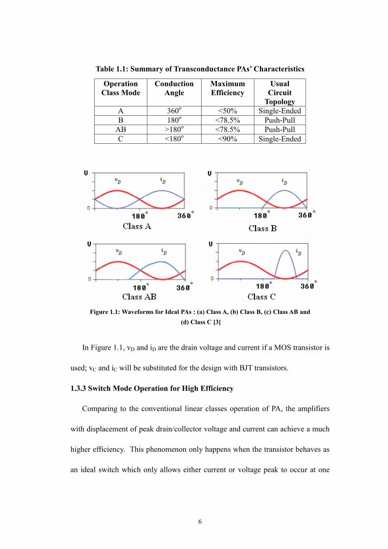
Table 1.1: Summary of Transconductance PAs’ Characteristics
Operation Class Mode
Conduction Angle
Maximum Efficiency
Usual Circuit
Topology A 360o <50% Single-Ended B 180o <78.5% Push-Pull
AB >180o <78.5% Push-Pull C <180o <90% Single-Ended
Figure 1.1: Waveforms for Ideal PAs : (a) Class A, (b) Class B, (c) Class AB and (d) Class C [3]
In Figure 1.1, vD and iD are the drain voltage and current if a MOS transistor is
used; vC and iC will be substituted for the design with BJT transistors.
1.3.3 Switch Mode Operation for High Efficiency
Comparing to the conventional linear classes operation of PA, the amplifiers
with displacement of peak drain/collector voltage and current can achieve a much
higher efficiency. This phenomenon only happens when the transistor behaves as
an ideal switch which only allows either current or voltage peak to occur at one

7
time. In such switching mode, power dissipation in the transistor can be totally
eliminated, and hence, achieving 100% efficiency, theoretically.
Unlike the linear PAs, switching mode operation requires that the output
voltage and current of the amplifier to be the transient response of a specially
designed output matching network to the time variant switch and a constant DC
power supply. In addition, switching implies that the output current and voltage
are discontinuous so that they have many higher order harmonic components.
Thus, a proper filtering scheme must be used to suppress the harmonics in order to
obtain high efficiency since they also dissipate power.
1.3.4 Class E and Its Advantages over other Classes of Power Amplifiers
Class E is a switching mode power amplifier. The concept was first proposed
and explored by Dr. Gerald Ewig in 1964 in his famous PhD dissertation “High-
Efficiency Radio-Frequency Power Amplifiers”. Later, Nathan and Alan Sokal
further developed the concept in 1975; Alan Sokal even patented it through the
article “Class-E New Class of High-Efficiency Tuned Single-ended Switching
Power Amplifiers”.
The most important advantage of class E power amplifiers is their ability to
provide high efficiency. Contrary to linear mode classes, class E can operate with
power loss smaller by a factor of 2.3 [4] at the same operating frequency to
provide the same amount of output power by using the same transistor. Then,
class E PA are relatively easy to design with a small size, light weight and relative

8
intolerance to circuit variation, which fulfill the requirement for system
miniaturization. Furthermore, class E power amplifier can be designed to operate
either at a specific frequency, i.e., narrow-band operation, or at a wide frequency
band, depending on the demand.
Currently, the design for class E operation up to Ku band has been
accomplished and engineers are struggling to push this up frequency limit even
higher.
1.4 Organization
This thesis is organized into six chapters. The fundamental concepts and the
need for the development of a Class E RF power amplifier prototype have been
discussed in this Chapter. Chapter 2 presents the basic Class E amplifier design
ideas, including its operation theories, circuit composition and functions. The
next two chapters, Chapter 3 and 4 address two design methods, linear and
nonlinear with respect to the output capacitance of the transistor, from the analysis
to theoretical designs in ADS simulations. Chapter 5 describes laboratory testing
and the corresponding results of the prototype using both design methods. The
concluding chapter summarizes the thesis work and contains some
recommendations for further research.

9
Chapter 2: Basic Class E Ideas
2.1 Common Class E RF Power Amplifier Configurations
There are two commonly used configurations of power amplifiers. They are
single-ended and complementary (also known as push-pull) illustrated as
Figure 2.1: Common Configurations of Power Amplifiers: (a) Single-ended; (b) Complementary (aka, push-pull)
A single-ended power amplifier has only one transistor, one load, one DC
power supply and one output filter network which is the major part of the device
responsible for its performance and functions. Compared to it, a push-pull mode
PA has two complementary transistors; thus, there will be a P-channel FET with
its drain connected to the DC power supply, its source to the drain of another N-
channel FET, whose source is grounded, and the rest PA circuit connected to the
intersection of the two FETs. They are arranged symmetrically. This is usually
called a CMOS configuration. Similarly, the PA composed of BJT transistors in
complementary mode will be configured by a PNP BJT connected to the DC

10
supply and then followed by a NPN BJT, as illustrated in (b) of Figure 2.1.
In this thesis, the single-ended configuration is used since the current standard
CMOS technology can not yield high efficiency power amplifiers because their
low breakdown voltage and strongly nonlinear parasitic drain-to-bulk output
capacitance make this type of PAs difficult to be implemented [5].
2.2 Optimum and Suboptimum Class E Operations
In Mr. Sokal’s article [4], he defines Class E power amplifier as a tuned power
amplifier composed of a single-pole switch and a load network. The load network
contains a series resonant LC circuit, a DC drain supply, and a drain shunt
capacitor. The load is simply a resistance. Preceding the load network is the
switch, which can either be a BJT or a FET. Ahead of the switch is the driver
circuit. The class E power amplifier developed by Mr. Sokal has the famous
circuit schematic as in Figure 2.2 below.
Figure 2.2: The Circuit Schematic of Class E PA Composed of a Single-Pole Switch and a Load Network Developed by Mr. Nathan Sokal [4]
In order to achieve a high efficiency, the peak of the current and voltage
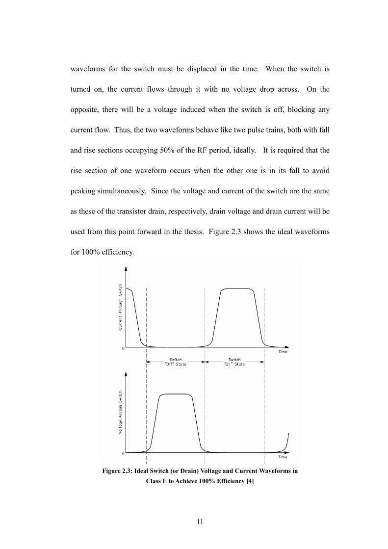
11
waveforms for the switch must be displaced in the time. When the switch is
turned on, the current flows through it with no voltage drop across. On the
opposite, there will be a voltage induced when the switch is off, blocking any
current flow. Thus, the two waveforms behave like two pulse trains, both with fall
and rise sections occupying 50% of the RF period, ideally. It is required that the
rise section of one waveform occurs when the other one is in its fall to avoid
peaking simultaneously. Since the voltage and current of the switch are the same
as these of the transistor drain, respectively, drain voltage and drain current will be
used from this point forward in the thesis. Figure 2.3 shows the ideal waveforms
for 100% efficiency.
Figure 2.3: Ideal Switch (or Drain) Voltage and Current Waveforms in Class E to Achieve 100% Efficiency [4]

12
Figure 2.3 reveals five conditions that must be realized for a high efficiency
operation.
1) The peak drain voltage and current do not exist simultaneously.
2) At the end of the rise section of the drain current waveform, it must
decrease to zero before the rise section of the voltage waveform can start.
In other words, the current reaches zero at the end of the ON interval right
before the switch is turned off. The beginning of the rise section of the
voltage waveform should be delayed until after the switch is turned off.
3) The slope of the current waveform at the end of its rise section must be
zero to avoid power dissipation due to the existence of both current and
voltage.
The similar conditions apply to the drain voltage waveform at the end of its
rise section.
4) It must return to zero at the end of the switch OFF interval (right before
the switch is turned on) before the rise of the current waveform can start.
The starting point of the rise section of the current waveform should be
postponed until after the transistor is turned on.
5) Its slope is zero at that moment to avoid power dissipation due to the
simultaneous imposition of current and voltage.
All the above five conditions are meant to eliminate the power dissipation of
the transistor as much as possible during the class E operation so that to increase

13
the efficiency. The realization of condition 1 reduces the majority power loss.
Condition 2 & 3 and 4 & 5 are aimed to decrease the power dissipation during the
ON to OFF and OFF to ON transitions of the switching process. They prevent the
energy loss from the coexistence of substantial current and voltage during the
transitions. Even though the power dissipation during the transition intervals is
small compared to that from the coexistence of peak voltage and current, it still
can decrease the efficiency dramatically, thus, degrade the class E performance.
The condition 2 and 3 are known as Zero Current Switching (ZCS) and Zero
Slope Current Switching (ZsCS), respectively, from the concepts of switching
regulator. Similarly, condition 4 and 5 are called Zero Voltage Switching (ZVS)
and Zero Slope Voltage Switching (ZsVS).
Practically, ZCS and ZsCS are very difficult to implement for frequencies
greater than a few decades of MHz. Therefore, switching condition set ZCS &
ZsCS and that for ZVS & ZsVS can not be achieved at the same time for high
frequencies. On the contrary, the latter set is much easier to design and implement.
Thus, the typical drain voltage and current waveforms for a practical class E
power amplifier look like the traces shown in Figure 2.4.

14
Figure 2.4: Drain Voltage and Current Waveforms of a Practical Class E PA
Figure 2.4 reveals a class E PA which realizes ZVS and ZsVS simultaneously,
but not ZCS and ZsCS. Thus, it can not reach 100% efficiency. However, its
efficiency is still very high because current flows through the switch when its
voltage is almost totally zero; most importantly, the peak drain current and peak
voltage are displaced in time.
Mr. Frederick H. Raab defined the class E PAs that meet all five conditions as
the optimum Class E [6]. He also proposed the definition of suboptimum Class E,
which is a class E power amplifier composed of a switch and a load network as in
Figure 2.2, however, not meeting those conditions. This allows a mistuned or not
optimized power amplifier to be classified as a class E. Similar to switching
condition set ZCS & ZsCS, in practice, optimum class E power amplifier is not
realizable for frequencies greater than a few tens of MHz. Yet, suboptimum class
E power amplifiers are designable and implementable.
15
2.3 Basic Circuit Schematic
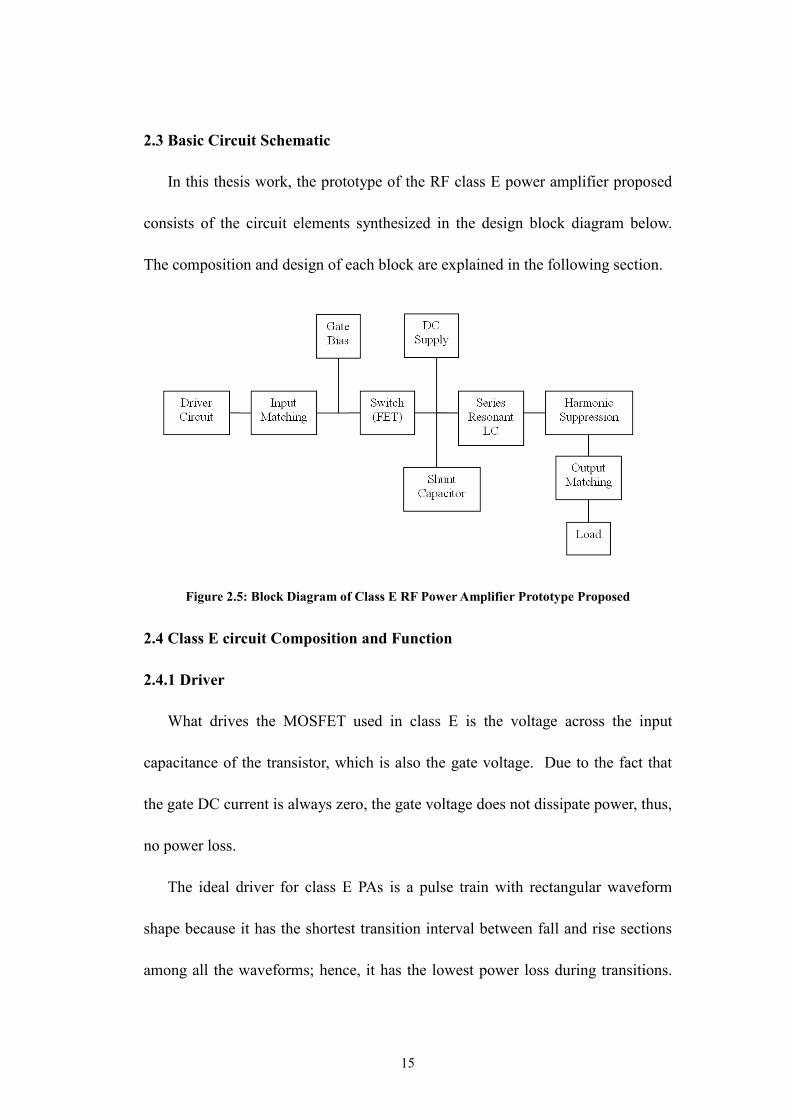
In this thesis work, the prototype of the RF class E power amplifier proposed
consists of the circuit elements synthesized in the design block diagram below.
The composition and design of each block are explained in the following section.
Figure 2.5: Block Diagram of Class E RF Power Amplifier Prototype Proposed
2.4 Class E circuit Composition and Function
2.4.1 Driver
What drives the MOSFET used in class E is the voltage across the input
capacitance of the transistor, which is also the gate voltage. Due to the fact that
the gate DC current is always zero, the gate voltage does not dissipate power, thus,
no power loss.
The ideal driver for class E PAs is a pulse train with rectangular waveform
shape because it has the shortest transition interval between fall and rise sections
among all the waveforms; hence, it has the lowest power loss during transitions.
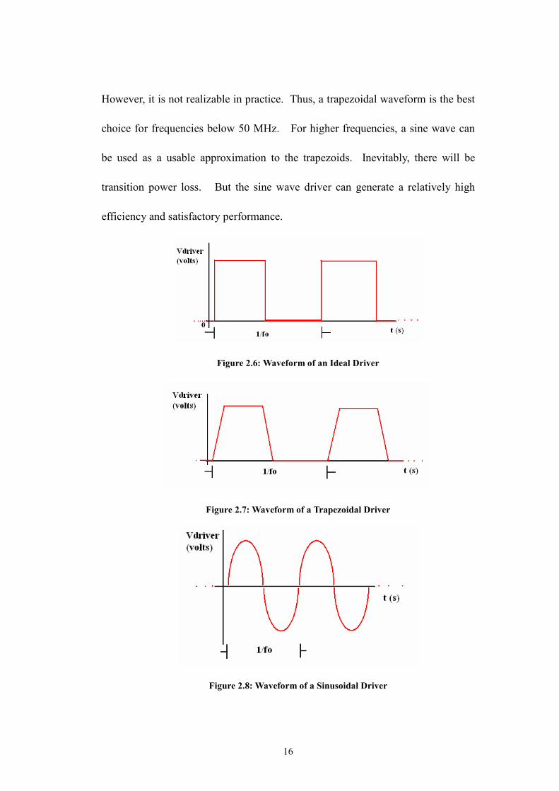
16
However, it is not realizable in practice. Thus, a trapezoidal waveform is the best
choice for frequencies below 50 MHz. For higher frequencies, a sine wave can
be used as a usable approximation to the trapezoids. Inevitably, there will be
transition power loss. But the sine wave driver can generate a relatively high
efficiency and satisfactory performance.
Figure 2.6: Waveform of an Ideal Driver
Figure 2.7: Waveform of a Trapezoidal Driver
Figure 2.8: Waveform of a Sinusoidal Driver

17
2.4.2 Input Matching
Input matching is required to reduce the reflection due to mismatch between
the impedance of the RF input source, the standard 50 Ω, and the impedance at the
right of 50 Ω when looking into the rest of the PA circuit. Let us define the RF
power available from the source to be PAV, and the power entering the power
amplifier as Pdel.
Since the power amplifier is always a part of a complex system, in which it is
always preceded and followed by some other devices with specific output power.
It is better to have the conjugate match between the RF power available from the
generator, or the output power from the device preceding the PA (PAV), and the
actual power entering the PA circuit (Pdel), for the purpose of accurately analyzing
the PA and the system’s performance, such as efficiency and gain.
2.4.3 Gate Bias
Since the gate voltage variations will drive the switch on and off, the gate bias
is important in supplying this swing. For a BJT acting as the switch in class E,
the transistor operates in cutoff and active region for OFF and ON interval,
respectively, each for a half RF switching period. The gate bias should be the DC
offset of the voltage waveform, which swings among the values needed for cutoff
and active, each for half time. For a FET switch, the transistor operates in cutoff
and saturation regions when the switch is in the OFF and ON stage, respectively.
Similarly, the gate bias should be the DC level of the swing which makes the

18
transistor to go cutoff or deep saturation.
2.4.4 Switch
Because the DC gate current is always zero of any MOSFET, the gate bias
circuit of a FET is easier to design then that of a BJT. Simply, the gate bias can be
a voltage divider composed of the resistors. Thus, FET is used as the switch in
this thesis work. Table 2.1 gives a summation of FETs that can be used in class E
PA design.
Table 2.1: FET Transistor Selection [7]
Transistor Drain BV (V)
Status Frequency Major Applications
Manufacturers
RF Power FET
65 Reliable for commercial
use
1 MHz – 400 MHz
VHF power amplifier & oscillator
Motorola
GaAs MeSFET
16-22, 60 Very reliable. 1 GHz – 30 GHz
Radar, satellite, military
Triquint, Eudyna, Excelics
SiC MeSFET
100 3 years old, Unproven reliability
500 MHz – 2.3 GHz
Base Station Cree
GaN MeSFET
160 Holy Grail. Still in
research stage.
1 GHz – 30 GHz
Replacement for GaAs
Cree, Triquint
Si LDMOS (FET)
65 Reliable for commercial
use
500 MHz – 2 GHz
Base station Cree, Freescale, Philips, Polyfet
Si VDMOS (FET)
65 – 1200 Reliable for commercial
use
1MHz – 500 MHz
HF & FM broadcast,
MRI
Polyfet, APT, IXYS
Based on the requirements for frequency and applications, a specific type of
FET will be chosen for a specific design. In addition, power output is important
in transistor selection, too, which is limited by the transistor’s drain breakdown
19
voltage and maximum current rating. These two parameters are determined
during the manufacturing process and are stated in the datasheet explicitly.
2.4.5 DC Supply
In class E power amplifier operation, the drain voltage will swing up to three
times of its DC supply voltage, sometimes even to reach or exceed the breakdown
voltage, resulting in the damage to the transistor and the amplifier circuit. Thus,
for the safe operation purpose, it is better that drain DC supply is less than a third
of the breakdown voltage, and greater than the gate DC bias.
2.4.6 RF Chocks
In class E design, there are two inductors connecting between the DC power
supply and the drain, and the bias voltage at the gate and the switch, respectively.
They act as short circuits at the DC and open circuits at the operating or the higher
frequencies. Thus, they block the RF signals going to the switch; in other words,
they only allow a constant D.C. current flowing from the DC power to the
transistor. Therefore, they are called RF chocks as their function is to “chock” (or
block) RF signals.
2.4.7 Load Network
The load network of Class E prototype proposed by this thesis is composed of
a drain shunt capacitance, a series resonant LC circuit, LC tank circuits for low
order harmonic suppressions, and an output matching network.
1) Drain Shunt Capacitance
20
The drain shunt capacitance, Cshunt, delays the starting point of the voltage rise
section while the current is at the end of its fall section during the ON to OFF
transition. It ensures that at the moment when the switch is turned OFF, the
voltage across the switch still remains relatively small as it was still at the end of
the fall section of the drain voltage, until after the drain current has reached zero.
Thus, its purpose is to shape the drain voltage and current waveforms during the
ON to OFF transition to make certain that there is as little power dissipation by
the switch as possible. The current flows for ON and OFF intervals around the
switch are explained below with the help of Figure 2.9 and 2.10.
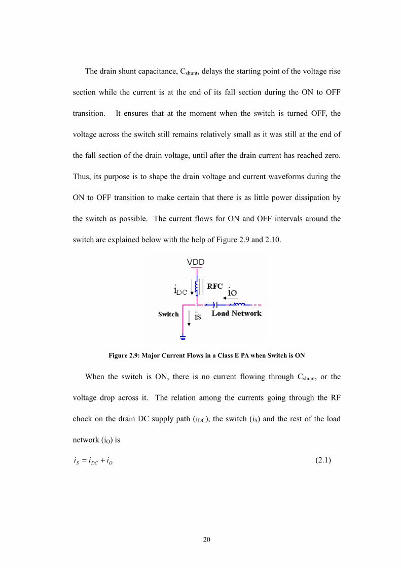
Figure 2.9: Major Current Flows in a Class E PA when Switch is ON
When the switch is ON, there is no current flowing through Cshunt, or the
voltage drop across it. The relation among the currents going through the RF
chock on the drain DC supply path (iDC), the switch (iS) and the rest of the load
network (iO) is
ODCS iii += (2.1)

21
Figure 2.10: Major Current Flows in a Class E PA when Switch is OFF
On the other hand, when the switch is OFF, iS becomes zero. All of the current
that flows through the switch when it is ON now flows through the drain shunt
capacitor, charging it up. Thus, the new current relation is
ODCC iii += (2.2)
At the switch OFF interval, the voltage across Cshunt is the same as the
transistor drain voltage, or the switch voltage. Thus, VS, VD and VCshunt are used
interchangeably in this thesis.
When the switch is turned on again, Cshunt is shorted immediately, causing it to
be discharged.
The drain shunt capacitance is mainly composed of the output capacitance of
the transistor and an external linear capacitance, Cex,l, in parallel with it. The rest
small portion of the composition comes from the transistor mounting capacitance,
the RF choke parasitic capacitance, and other stray capacitances. Since this
portion is very small, it is usually ignored in the design.
The required external linear capacitance decreases as the operation frequency

22
increases. Thus, at high frequencies, Cshunt is often partially or, sometimes
completely, absorbed by the transistor’s output capacitance, Cout. At that case,
Cshunt will not be connected in the circuit of the design. Cout alone provides
enough drain shunt capacitance for the optimal Class E operation.
2) Series Resonant LOCO Circuit
The series resonant LOCO circuit resonates at a slightly smaller frequency than
the PA’s operating frequency, fo. Typically, LO consists of two inductors, Lr and Le
with Lr as the dominant composite. Lr together with CO resonates at fo,
guaranteeing a substantially sinusoidal load current; and Le is the excess
inductance makes sure that ZVS and ZsVS conditions are met to eliminate the
energy loss. In addition, it causes a phase shift between the sinusoidal load
current and the fundamental component of the applied drain voltage.
The relationship between CO, LO, Lr, Le and Cshunt can be explained as
following:
erO LLL += (2.3)
When the switch is closed, the drain shunt capacitance is shorted; thus, the
series LOCO circuit resonates at fL, smaller than the resonate frequency of COLr
and the corresponding schematic of load network is shown in Figure 2.11.
rOo LC
fπ2
1= (2.4)
OOL LC
fπ2
1= < 0f (2.5)
23
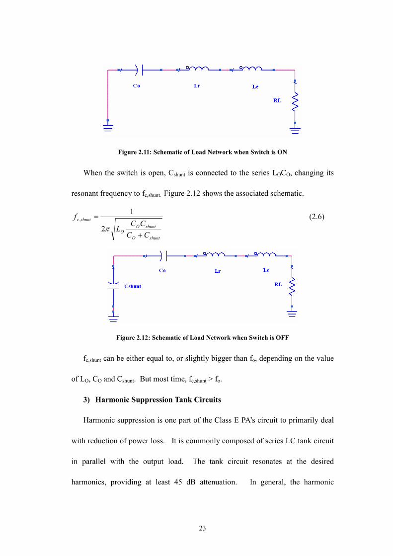
Figure 2.11: Schematic of Load Network when Switch is ON
When the switch is open, Cshunt is connected to the series LOCO, changing its
resonant frequency to fc,shunt. Figure 2.12 shows the associated schematic.
shuntO
shuntOO
shuntc
CCCCL
f
+
=
π2
1, (2.6)
Figure 2.12: Schematic of Load Network when Switch is OFF
fc,shunt can be either equal to, or slightly bigger than fo, depending on the value
of LO, CO and Cshunt. But most time, fc,shunt > fo.
3) Harmonic Suppression Tank Circuits
Harmonic suppression is one part of the Class E PA’s circuit to primarily deal
with reduction of power loss. It is commonly composed of series LC tank circuit
in parallel with the output load. The tank circuit resonates at the desired
harmonics, providing at least 45 dB attenuation. In general, the harmonic

24
attenuation is expressed in dBc, which is the difference in dB between the inter-
modulation (IM) power and the fundamental frequency power.
Since the harmonic impedances of a Class E PA are the result of Cshunt and
decrease with frequency, and the third and higher harmonics are of relatively
small amplitudes, in most cases, only one LC tank circuit is needed, which
resonates at 2fo. However, sometimes a second tank circuit is implemented for
third harmonic if its power level compared to fundamental is smaller than 45 dBc
in difference.
4) Output Matching
Output matching in Class E is usually needed if the required load impedance is
other than the standard RF load, 50 Ω, associated with SMA connectors. Because
the matching is done between only two real impedances, the simple L-section
lumped elements matching circuit can be used.
The L-section matching network requires only a capacitor and an inductor.
There are two configurations and the applications depend on whether the PA’s
load resistance is bigger or smaller than 50 Ω. But the design equations are the
same. Figure 2.13 plots the design schematics and Equations 2.7 and 2.8 are used
to find the circuit component values.
25
Figure 2.13: L-Section Matching Networks for Two Resistive Impedances: (a) L-Section to Match a Low Resistance to a High Resistance; (b) L-Section to Match a High Resistance to a
Low Resistance
P
HL
L
S
XRQ
RX
== (2.7)
12 += LL
H QRR
(2.8)
Where, QL is the loaded quality factor of LC, which has to be small compared
with the unloaded Q factor of the components. XS is the series inductance and XP
is the parallel capacitance of the matching network. RH and RL are the high and
low resistances to be matched; one will be 50 Ω and the other one will be the
Class E PA’s required load resistance.
2.4.8 Load
A resistive load is implemented in Class E PA at the output terminal. Besides
the resistance from the design equations, which will be addressed in the next
chapter, the load must include all of the parasitic resistances, the equivalent series
resistance (ESR) of the inductors at the operating frequency in the circuit for high
frequency operation. ESR resistances change with respect to the frequency; they
increase as operating frequency increases, but not in a linear way. Being able to

26
accurately model the behavior and predict the values of ESR in the circuit can
prevent additional energy loss because similar to regular resistors, ESRs dissipate
power when current is flowing through them.

27
Chapter 3: Class E PA Circuit Design Analysis with Linear Drain
Shunt Output Capacitance
Mr. Nathan Sokal and Mr. Alan Sokal are the very first people who explored
the concepts of Class E RF power amplifier in the middle 70’s. They analyzed the
circuit of this type power amplifier exclusively and provided very useful and
valuable analysis equations. Most importantly, they assumed the transistor output
capacitance is linear. Thus, the name, Linear Design Method or Liner Design
Analysis, is used throughout the thesis to refer to the method proposed by two Mr.
Sokal. This circuit analyzing method is applicable for operation frequency below
900 MHz. The design equations [4] will be re-stated in the next section with some
modifications to fit the design in this thesis work.
3.1 Linear Design Analysis for Class E PA Operations
In Mr. Nathan Sokal’s famous article “Class E RF Power Amplifiers” [4], he
gave 5 equations for determining the component values of a class-E amplifier
using BJT transistors. The corresponding equations for Class E design using FET
transistors are below.
SFBVV DSVDD
=
56.3(3.1)
Equation 3.1 gives the voltage supply to be used. VDD is the drain supply
voltage, BVDSV is the breakdown voltage of the FET to be used, and SF is the
safety factor.

28
−−
= 2
2 402444.0414395.0001245.1576801.0LLout
DDL QQP
VR (3.2)
Equation 3.2 gives the value of resistance for the load that is to be used. VDD
is the supply voltage given by Equation 3.1. Pout is the output power desired. QL
is the loaded quality factor of the series LOCO resonant circuit.
( ) 122 2
6.003175.191424.099866.02219.34
1LfQQRf
CoLLLo
shunt π+
−+= (3.3)
Equation 3.3 gives the value of Cshunt, which is the drain shunt capacitance.
According to Mr. Sokal, this Cshunt should also include any output capacitance
associated with the transistor. fo is the center/operating frequency. RL is the
resistance calculated from Equation 3.2. QL is the loaded quality factor. L1 is the
RF chock at the drain. Mr. Sokal did not give explicit equations about how to
calculate this inductance. Instead, he proposed that the values of RFC can be
chosen as long as its impedance at fo and higher frequencies is big enough that we
can assume there is an open circuit. Then, any AC signal and AC power will be
blocked by L1 and there is only a constant DC current flowing in the drain power
supply path.
( ) 122
2.07879.1
01468.100121.1104823.01
21
LfQQRfC
oLLLoO ππ
−
−
+
−
= (3.4)
Equation 3.4 gives the value of CO, the capacitance in the series LOCO
resonant circuit. fo is again the operating frequency. RL is the load resistance
from Equation 3.2. QL is the loaded quality factor. L1 is the DC feed RF choke.
29
o
LLO f
RQLπ2
= (3.5)
Equation 3.5 gives the value of LO, the total inductance in the series resonant
circuit. fo is the operating frequency. RL is the resistance from Equation 3.2. QL
is the loaded quality factor.
Using the notations for the calculations above, the schematic for the main part
of Class E power amplifier from Mr. Sokal’s design analysis can be shown as in
Figure 3.1 below, which is just the modified version of the schematic in Figure 2.2
in Chapter 2.
Figure 3.1: Circuit Schematic of Class E RF PA Using Linear Design Analysis Method
Those design equations are used to calculate load resistance RL, the drain
shunt capacitor Cshunt, and LO and CO in the resonant circuit for a desired operating
frequency fo, loaded quality factor QL, output power Pout, input power from the
source generator Pin, drain power supply VDD and RF Choke at drain L1.

30
3.2 Circuit Design by Using Linear Method
For this thesis work, the Class E power amplifiers for operating frequencies of
100 kH, 1 MHz, 10 MHz and those with a factor of 10 increments afterwards till
150 MHz are designed by using linear method and simulated in Advanced Design
System (ADS) from Agilent Technologies. Thus, there are total 17 theoretical
designs. However, only these two at 10 MHz and 150 MHz are actually
implemented in the laboratory; the detail will be addressed in the Chapter 5.
3.2.1 General Circuit Parameter Selections for Theoretical Design in ADS
Driver
For all the 17 cases, a sinusoidal waveform at the designated operating
frequency is employed in simulation. In addition, a preamplifier generating a
trapezoidal waveform is designed and used as the driver for 10 MHz case.
Similarly, a preamplifier outputting a saw shape waveform is used to drive the 150
MHz Class E power amplifier.
Basically, the preamplifier is a modified Class A RF power amplifier using
another FET transistor. Its circuit configuration is very similar to that of a class E,
but much simpler; there is a sine input, a gate bias, a drain DC power supply and
an output load as indicated in Figure 3.2.
31
Figure 3.2: Configuration of Class A RF Power Amplifier Used in Thesis Work
Theoretically, a Class A RF power amplifier accepts a sinusoidal input and
outputs another sinusoid at the same frequency but with much greater amplitude
and their phase difference remains constant during the entire amplification process.
Thus, the transistor must operate in the saturation region of a FET only and its
input must be small enough that it will not be able to drive the transistor into
cutoff.
However, in order to have a trapezoidal waveform at the output of an
amplifier in generic Class A configuration, the input signal should be big enough
to drive the transistor as a switch, which operates between the saturation and
cutoff regions. Hence, it requires the FET gate bias to be around its threshold for
turning on as well. The preamplifier designed for the 10 MHz case is shown in
Figure 3.3.
32
Figure 3.3: Preamplifier for 10 MHz Design
In Figure 3.3, 3.5 V and 4.75 V are the gate bias and drain DC power supply,
respectively; the L-network composing of a 1.69 µH inductor and a 118 pF
capacitor is the input matching network to match the actual power delivered to the
preamplifier to the power from the generator, which is 50 mW. The series 0.1 uF
capacitors are for DC blocking and those parallel ones are for bypassing. The
series RL configuration and the bypass capacitor at the gate bias together ensure
the low frequency stability of the device.
The preamplifier for the 150 MHz case has the same circuit configuration as
that in Figure 3.3, but with different component values. Furthermore, when the
frequency is increased from 10 MHz to 150 MHz, even though the transistor is
still driven to operate between cutoff and saturation, a trapezoidal waveform is not
generated any more; instead, a saw waveform resulted because the switching
becomes non-ideal as frequency increases.

33
Switch
RF power FET, MRF134, is chosen for this thesis work because of its high
drain breakdown voltage (65 V), big allowable gate voltage swing (± 40 V), and
VHF frequency operation band (1 MHz – 400 MHz) [8]. In addition, RF power
FET has the advantages of high gain, low noise, simple gate bias, and ability to
withstand severely mismatched loads without damage. Furthermore, it can yield a
wide range of output power with a low power DC control signal. By correctly
changing its gate bias DC voltage, MRF134 can supply an output power from its
maximum rating value down to zero.
ADS has both the Spice and S-parameter models of MRF134 transistor. Thus,
the designer can simulate and evaluate the theoretical design thoroughly before
actually building the circuit. The simulation results can be used as the check
points for the experimental measurements as well. MRF134 has a simple
footprint, and easy to be implemented on the printed circuit board (PCB).
However, it has two major drawbacks compared to other RF power FETs. Its size
is big 0.81” X 0.81” (width X length), and it can only output 9 watts maximally
when the operation conditions and the design are correct. Nevertheless, its
characteristics are sufficient for the prototype design of Class E RF PAs.
1) The DC-IV Curves of MRF134
The MRF134 transistor has the following drain-to-source voltage (VDS)
verses drain-to-source current (IDS) characteristics for several values of gate-to-
34
source DC voltages.
5 10 15 20 25 30 350 40
20
40
60
80
0
100
VGS=2.000VGS=2.300VGS=2.600VGS=2.900VGS=3.200VGS=3.500
VGS=3.800
VGS=4.100
VGS=4.400
VGS=4.600
VDS, V
IDS,
mA
DC-IV Curves
Figure 3.4: VDS vs. IDS of MRF134 for VGS from 2.0 V to 4.6 V
We call the curves in Figure 3.4 as DC-IV curves. Figure 3.4 is generated by
using the root model of MRF134 on the ADS. 0V to 36 V with a 1 V increment is
input to the drain as the VDS and 2.0 V to 4.6 V with 0.3 V increment to the gate as
the VGS. Under such voltage input ranges, Figure 3.4 indicates that when the VDS
is greater than 2.5 V and VGS exceeds 3.5 V, there is a relatively constant current
flowing from drain to source for a constant VGS and the transistor is saturated.
The triode mode of MRF134 is very brief; it only happens for the VDS values
between 0 V and 2.5 V and for VGS greater than the threshold.
The DV-IV curves for an ideal MOSFET transistor should have absolutely
constant IDS for a fixed VGS value and IDS is totally independent of VDS in
saturation region as in the figure below because the channel pinch-off occurs.

35
2 4 6 8 10 12 14 16 180 20
0.5
1.0
1.5
2.0
2.5
0.0
3.0
VGS=-2.000VGS=-1.600VGS=-1.200VGS=-0.800VGS=-0.400
VGS=1.110E-16
VGS=0.400
VGS=0.800
VGS=1.200
VGS=1.600
VGS=2.000
VDS (V)
ID(A
)
Figure 3.5: DC-IV Curves for an Ideal MOSFET
Ideal DC-IV characteristics do not exist due to the fact there is no ideal
MOSFET. In general, IDS has some dependence on VDS in saturation mode
because of the Channel Length Modulation associated with MOSFET transistors;
IDS increases with the increase in VDS slightly. Thus, those horizontal lines in
Figure 3.4 will incline toward left a little bit as in Figure 3.5, which is created by
employing a practical MRF134 model.
The DV-IV curves are totally independent of the operating frequency. Hence
the same curves are used for all 17 design cases.
Gate Bias
As exhibited in Figure 3.4 and [8], the typical gate threshold voltage, the
critical value to turn the transistor MRF134 on, is 3.5 V. In order to guarantee that
the switch is OFF when it is not ON, either 3 V, a value below the threshold a little
bit, or 3.5 V is used as the gate DC bias for the designs. Thus, the gate voltage
36
swings between the values that drive the transistor into cut off and saturation
region each for half of the RF switching period.
20 40 60 80 100 120 140 160 1800 200
-5
0
5
10
15
-10
20
t, ns
Vgat
e,V
Figure 3.6: Gate Voltage Swing for 10 MHz Class E Linear Design Using MRF134
When 3 V is used at the gate and 100 mW as the input power to a Class E RF
PA design at 10 MHz, the corresponding gate voltage swing is in Figure 3.6,
which has a DC offset around 3 V. Thus, the transistor is on and off for 50% of
the time individually.
DC Supply
Using Equation 3.1, the theoretical drain DC supply voltage with the safety
factor equal to 1.0 is 18.26 V. Using a third of the breakdown voltage of the
transistor MRF134, it should be less than 21.67 V. The power suppliers in the lab
at CReSIS can provide maximum 25 V. Thus, any value that is equal to or below
25 V and does not generate a drain voltage swinging close to breakdown when
operating with other circuit elements in PA, can be used as the drain DC power
supply. In fact, higher DC voltage supply provides higher output power if

37
designed correctly.
For 17 operating frequency cases, DC voltages within 15 V to 23 V are used as
the supply voltage for different designs.
RF Chokes
There is no explicit equation proposed by Mr. Sokal for the values of RF
chokes. However, it is advisable to use big inductances so that the inductors can
operate as open circuits at fo, ideally. Thus, in ADS simulation, 1mH is used for
design cases with fo up to 60 MHz, 0.1 mH for 60 MHz and 70 MHz cases, and 50
µH for fo from 80 MHz to 150 MHz. Then, the impedances of those RF chokes
are at least 47 kΩ, big enough to prevent current flows through it.
However, it is not feasible to use big value inductances in practice because
they invertibly have series equivalent resistances which change with respect to
frequency; therefore, they impact the design results dramatically. This will be
addressed in Chapter 5 later.
Input Matching
ADS is able to tell the values of the current flowing through and the voltage
across any circuit component and at any node by using current and voltage probes,
respectively. When putting those two at the beginning of the power amplifier
circuit right after the source, or the power generator, the power delivered to the
power amplifier circuit from the generator, Pdel, can be calculated as:
38
2||*|| inputinput
del
IVP = (3.6)
Where, Vinput and Iinput are the AC input voltage and current respectively and | |
is the magnitude calculation symbol.
Figure 3.7: Measuring Vinput & Iinput in ADS
Once the Pdel is obtained, and with PAVL (the power available from the source
generator) set by the designer, the impedance ratio between the source resistance,
RS, which is a standard 50 Ω, and the resistance looking at the input of the PA
circuit, Rin, will simply be the square root of the ratio of PAVL to Pdel.
Consequently, the value of Rin can be acquired easily as
AVL
delSin P
PRR *= (3.7)
Then, the input matching network can be design by using Equation 2.7 and 2.8
with either configuration in Figure 2.13. Once Pdel is matched with PAVL, they are
equal to each other and Pin is used to denote the input power when this match
occurs.
inmatchedAVLdel PPP == | (3.8)

39
Load
For all 17 cases, the calculations for the circuit element values are done by
using the operating conditions: Pout = 5 W, QL = 5, VDD = 15 V and VGG = 3 V.
Thus, according to Equation 3.2, the resultant load resistance, RL, which is only
dependent of Pout, QL and VDD, is the same for all cases, which is 23.225 Ω.
Load Network
The drain shunt capacitance, Cshunt, and CO and LO in the series resonant
circuit, can be obtained by using Equation 3.3, 3.4 and 3.5, respectively.
The tank circuits for 2nd and sometimes 3rd harmonic suppression are obtained
by using
1)2( ,tan,tan2 =nknk CLnfπ (3.9)
Where, n represents the order of the harmonics. After the value of either
Ltank,n or Ctank,n is chosen, the other one can be calculated using Equation 3.8. The
tank circuits are series LC resonant at the nth harmonic frequency. It is
recommended to pick big inductors which result in sharp resonance, thus, great
harmonic attenuation.
The output matching is done easily for these 17 cases because both
resistances for matching are known; they are 50 Ω for the standard RF connector
and 23.225 Ω load resistance as calculated using linear analysis. Then, the
matching design will be followed by the method addressed in Chapter 2.

40
3.2.2 Performance Evaluating Parameters for Class E RF Power Amplifiers
There are five important parameters used to evaluate the performance of a
Class E RF power amplifier. They are DC power from the power supply, output
power, power gain, efficiency and the 2nd and 3rd harmonic attenuations. Even
though the desired output power, Pout, is used in Equation 3.2 for the calculation of
RL, it is in general not the output power generated after all the component values
have been decided, which is much more important than former.
DC Power
According to the design block diagram in Figure 2.5, there are two DC voltage
supplies used in the PA circuit, the gate bias and the drain DC supply. However,
the nature of the FET transistor requires no current flow at the gate. Hence, there
is no power supplied to the circuit by the gate bias. Using the probes in ADS at
the drain, the corresponding DC current and voltage can be measured and thereof
the DC power, PDC which is the same as the drain supply power PDD, can be
obtained as
DDDDDCDC PVIP == * (3.10)
Output Power (i.e., Load Power)
When the current and voltage probes are used at the load of a PA design in
ADS, the output power, Pout, can be found easily.
2||*|| loadload
outIVP = (3.11)

41
Where, Vload and Iload are the AC input voltage and current respectively and | |
is the magnitude calculation symbol.
Power Gain
Once the output power is found and the input power from the source generator
is known, the power gain, G, of a Class E power amplifier is the ratio between
these two values as
in
out
PP
G = (3.12)
Almost all the time, the power gain is expressed in dB scale as a convention
)(log10 10in
out
PP
G = (3.13)
Efficiency
In general, the efficiency of any amplifier is called the power-conversion
efficiency and defined as the ratio between the output power to the supply power
)()(
S
out
PrSupplyPowePrOutputPowe
=η (3.14)
In class E design, Equation 3.14 will be altered specifically by using drain
supply power as the denominator and the load power as the numerator. It then
becomes the definition of the drain efficiency for a FET class E power amplifier.
The modified equation is
DC
out
DD
outd P
PPP
yPowerDrainSupplLoadPower
===η (3.15)
Due to the existence of harmonics and the filtering circuits to attenuate them,

42
the RF fundamental power is a very good approximation for Pout.
In addition, power-added efficiency, PAE, is used most of the time to evaluate
the performance of class E PAs along with ηd. Unlike drain efficiency, PAE takes
into account of the RF input source power, Pin, as well.
DC
inout
PPPPAE −
= (3.16)
According to Equation 3.16, a power amplifier with a greater Pin will have a
smaller PAE and a smaller power gain than the one with a smaller Pin, for the
same amount of output power. But their ηd will be the same.
Similar to PAE, the overall efficiency, ηall, also accounts for Pin. It is the ratio
of the output power to the sum of the DC and the RF input power.
inDC
outall PP
P+
=η (3.17)
Again, high ηall requires a small Pin if the DC and output power are fixed.
2nd and 3rd Harmonic Attenuation
ADS has embedded functions to calculate the load voltage at nth harmonic and
at the fundamental frequency. The harmonic attenuation can be obtained by
taking the ratio between the fundamental load and nth harmonic voltages and the
result is expressed in dBc as
)(log20,,
10harn
fattth V
Vn −= (3.18)
Where, nth,att is the attenuation for nth harmonic, Vf is the fundamental load

43
voltage and Vn,har is the nth load harmonic voltage.
3.2.3 ADS Simulation for 17 Cases with Calculated Circuit Elements Using
Linear Design Method
Using Equation 3.2, 3.3, 3.4 and 3.5 to calculate RL, Cshunt, CO and LO values
for each fo with the conditions QL =, VDD = 15 V, VGG = 3 V, Pin = 100 mW, L1
values chosen as explained in Subsection 3.2.1, and desired Pout = 5 W, the
calculation and simulation results, i.e., DC power, output power, power gain,
efficiencies, and 2nd and/or 3rd harmonic attenuations, for 17 cases of Class E RF
power amplifiers with the configuration in Figure 3.1, which has no input and
output matching networks and no tank circuits for harmonics, are summarized in
the Table 3.1 and 3.2, respectively. Because the load resistance for all the cases is
23.225 Ω, it is not listed in the table. In addition, the power delivered to the PA
circuit from the source generator, Pdel, and the DC current measured at the drain
DC supply path in ADS, IS_H, are also listed in the table.
44
Table 3.1: Calculation Results of 17 Cases Using Linear Design Analysis
fo (MHz) Cshunt (pF) CO (pF) LO (µH) 0.1 14.45X10³ 18.40X10³ 184.82 1 1.44X10³ 1.84X10³ 18.48 10 143.61 184.33 1.85 20 71.732 92.19 0.924 30 47.84 61.45 0.616 40 35.87 46.09 0.462 50 28.70 36.87 0.370 60 23.91 30.73 0.308 70 20.53 26.33 0.264 80 17.98 23.03 0.231 90 15.98 20.47 0.205 100 14.38 18.43 0.185 110 13.07 16.75 0.168 120 11.98 15.36 0.154 130 11.05 14.18 0.142 140 10.26 13.17 0.132 150 9.58 12.29 0.123
Table 3.1 reveals that Cshunt decreases as frequency increases and its
decreasing rate is the same as the increasing rate of fo. The same phenomena
occur to CO and LO. The analytical equation of Cshunt, Equation 3.3, has two terms,
both of them are inversely proportional to fon, where n is the power factor.
However, the second term is much smaller than the first; therefore, the value of
Cshunt is inversely proportional to the first power of fo, so is CO in Equation 3.4 and
LO in Equation 3.5.
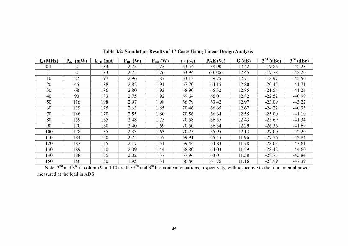
45
Table 3.2: Simulation Results of 17 Cases Using Linear Design Analysis
fo (MHz) Pdel (mW) IS_H (mA) PDC (W) Pout (W) ηd (%) PAE (%) G (dB) 2nd (dBc) 3rd (dBc)0.1 2 183 2.75 1.75 63.54 59.90 12.42 -17.86 -42.281 2 183 2.75 1.76 63.94 60.306 12.45 -17.78 -42.2610 22 197 2.96 1.87 63.13 59.75 12.71 -18.97 -45.5620 45 188 2.82 1.91 67.70 64.15 12.80 -20.45 -41.7130 68 186 2.80 1.93 68.90 65.32 12.85 -21.54 -41.2440 90 183 2.75 1.92 69.64 66.01 12.82 -22.52 -40.9950 116 198 2.97 1.98 66.79 63.42 12.97 -23.09 -43.2260 129 175 2.63 1.85 70.46 66.65 12.67 -24.22 -40.9370 146 170 2.55 1.80 70.56 66.64 12.55 -25.00 -41.1080 159 165 2.48 1.75 70.58 66.55 12.43 -25.69 -41.3490 170 160 2.40 1.69 70.50 66.34 12.29 -26.36 -41.69100 178 155 2.33 1.63 70.25 65.95 12.13 -27.00 -42.20110 184 150 2.25 1.57 69.91 65.45 11.96 -27.56 -42.84120 187 145 2.17 1.51 69.44 64.83 11.78 -28.03 -43.61130 189 140 2.09 1.44 68.80 64.03 11.59 -28.42 -44.60140 188 135 2.02 1.37 67.96 63.01 11.38 -28.75 -45.84150 186 130 1.95 1.31 66.86 61.75 11.16 -28.99 -47.39Note: 2nd and 3rd in column 9 and 10 are the 2nd and 3rd harmonic attenuations, respectively, with respective to the fundamental power
measured at the load in ADS.

46
Even though there is an inverse proportional relationship between fo and the
circuit component values, there is no such conspicuous relations between the
operating frequency and the performance evaluating parameters.
The drain voltage verses time and drain current verses time plots of all 17
cases are attached at the Appendix A.1. From these plots, several observations can
be made. 1) Most obviously, as fo increases, the current and voltage waveforms
deviated from the ideal shapes; they smear out more so that the transitions for both
ON to OFF and OFF to ON need more time to perform. This indicates that it is
getting hard to switch between ON and OFF promptly for the transistor as
frequency goes up. 2) As fo increases, the voltage waveform peaks lower and the
current goes down below 0 more; 3) as fo increases, the current waveform changes
toward a sinusoid more. Thus, circuit optimization is needed in order to make the
designs change toward optimum operations.
3.2.4 Design Optimization
There are two ways to optimize the designs employed in this thesis. First, the
matching networks for both input and output and the tank circuits for harmonic
suppression are added to the design in the previous sections, aiming at increasing
the efficiency. Then, the circuit values are tuned to achieve ideal drain voltage
waveform for optimum operation.
Additions of Matching Networks and Tank Circuits
For all 17 cases, Pdel values are listed in Table 3.2. They are different for
47
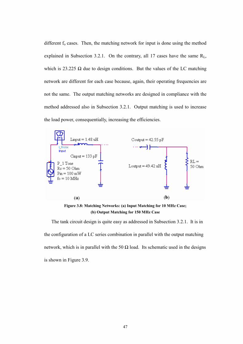
different fo cases. Then, the matching network for input is done using the method
explained in Subsection 3.2.1. On the contrary, all 17 cases have the same RL,
which is 23.225 Ω due to design conditions. But the values of the LC matching
network are different for each case because, again, their operating frequencies are
not the same. The output matching networks are designed in compliance with the
method addressed also in Subsection 3.2.1. Output matching is used to increase
the load power, consequentially, increasing the efficiencies.
Figure 3.8: Matching Networks: (a) Input Matching for 10 MHz Case; (b) Output Matching for 150 MHz Case
The tank circuit design is quite easy as addressed in Subsection 3.2.1. It is in
the configuration of a LC series combination in parallel with the output matching
network, which is in parallel with the 50 Ω load. Its schematic used in the designs
is shown in Figure 3.9.

48
Figure 3.9: Tank Circuit for 2nd and 3rd Harmonic Suppressions with Output Matching and Load Resistance for 150 MHz Case
Circuit Tuning
Both [4] and [9] address the method to tune the circuit values of Class E RF
power amplifier so that its drain voltage waveform can resemble the ideal one
more and therefore the circuit can function toward the optimum performance more.
The tuning is mainly focus on the values of Cshunt, CO, LO and RL because they
affect the waveform shape directly. In addition, the drain supply voltage, the gate
bias, the component values in the matching circuits, and those in the tank circuits
are also tuned for further improvements in both efficiency and waveform shapes.
Figure 3.10 shows the tuning mechanism for Cshunt, CO, LO and RL.
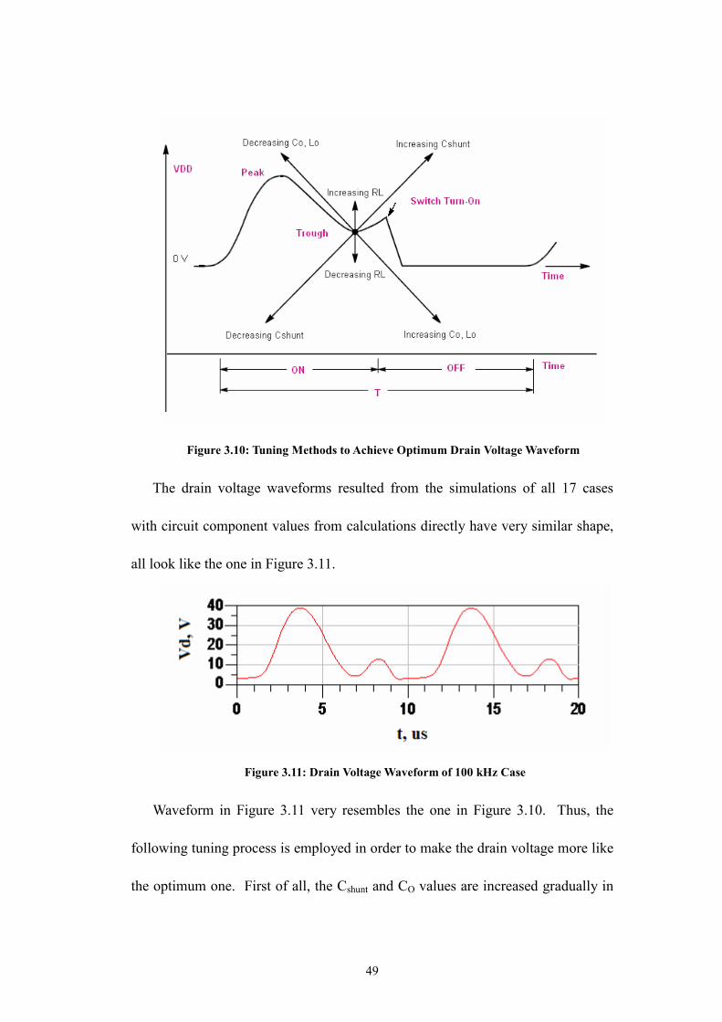
49
Figure 3.10: Tuning Methods to Achieve Optimum Drain Voltage Waveform
The drain voltage waveforms resulted from the simulations of all 17 cases
with circuit component values from calculations directly have very similar shape,
all look like the one in Figure 3.11.
Figure 3.11: Drain Voltage Waveform of 100 kHz Case
Waveform in Figure 3.11 very resembles the one in Figure 3.10. Thus, the
following tuning process is employed in order to make the drain voltage more like
the optimum one. First of all, the Cshunt and CO values are increased gradually in

50
proportions so that the small peak near the transition will become smaller and
smaller and eventually disappears. Then, the Cshunt value is decreased by the
amount of Coss as stated in the Datasheet of the MRF134 transistor [8] to account
for its output capacitance. This brings in only a slight change in the waveform.
Subsequently, the values of LO and RL are changed according to the method in
Figure 3.10 and the drain DC supply voltage as well as the RFC values is also
tuned for higher load output power. Consequently, the output matching network
values are varied slightly for better waveform shape. The optimization simulation
results are summarized in the next section.
3.2.5 Results from Optimization Using Linear Method
The optimization methods in the previous subsection both increase the
efficiency and improve the drain voltage waveform for all 17 cases more or less.
The tuning process stops when changing the circuit values any further will not
increase the efficiency, nor improve the waveform shape any more. The drain
waveforms of both voltage and current for 10 MHz and 150 MHz after circuit
optimization are shown in Figure 3.12. Others are listed in Appendix A.2.
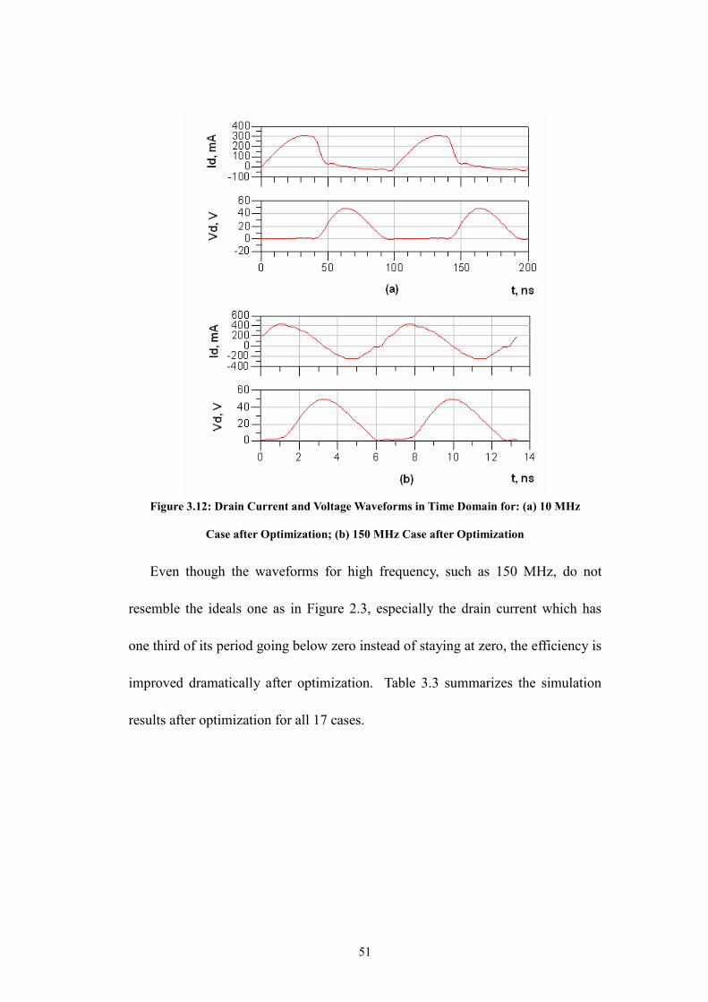
51
Figure 3.12: Drain Current and Voltage Waveforms in Time Domain for: (a) 10 MHz
Case after Optimization; (b) 150 MHz Case after Optimization
Even though the waveforms for high frequency, such as 150 MHz, do not
resemble the ideals one as in Figure 2.3, especially the drain current which has
one third of its period going below zero instead of staying at zero, the efficiency is
improved dramatically after optimization. Table 3.3 summarizes the simulation
results after optimization for all 17 cases.
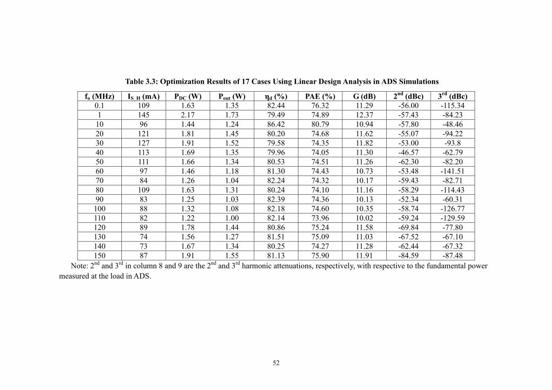
52
Table 3.3: Optimization Results of 17 Cases Using Linear Design Analysis in ADS Simulations
fo (MHz) IS_H (mA) PDC (W) Pout (W) ηd (%) PAE (%) G (dB) 2nd (dBc) 3rd (dBc)0.1 109 1.63 1.35 82.44 76.32 11.29 -56.00 -115.341 145 2.17 1.73 79.49 74.89 12.37 -57.43 -84.2310 96 1.44 1.24 86.42 80.79 10.94 -57.80 -48.4620 121 1.81 1.45 80.20 74.68 11.62 -55.07 -94.2230 127 1.91 1.52 79.58 74.35 11.82 -53.00 -93.840 113 1.69 1.35 79.96 74.05 11.30 -46.57 -62.7950 111 1.66 1.34 80.53 74.51 11.26 -62.30 -82.2060 97 1.46 1.18 81.30 74.43 10.73 -53.48 -141.5170 84 1.26 1.04 82.24 74.32 10.17 -59.43 -82.7180 109 1.63 1.31 80.24 74.10 11.16 -58.29 -114.4390 83 1.25 1.03 82.39 74.36 10.13 -52.34 -60.31100 88 1.32 1.08 82.18 74.60 10.35 -58.74 -126.77110 82 1.22 1.00 82.14 73.96 10.02 -59.24 -129.59120 89 1.78 1.44 80.86 75.24 11.58 -69.84 -77.80130 74 1.56 1.27 81.51 75.09 11.03 -67.52 -67.10140 73 1.67 1.34 80.25 74.27 11.28 -62.44 -67.32150 87 1.91 1.55 81.13 75.90 11.91 -84.59 -87.48
Note: 2nd and 3rd in column 8 and 9 are the 2nd and 3rd harmonic attenuations, respectively, with respective to the fundamental powermeasured at the load in ADS.
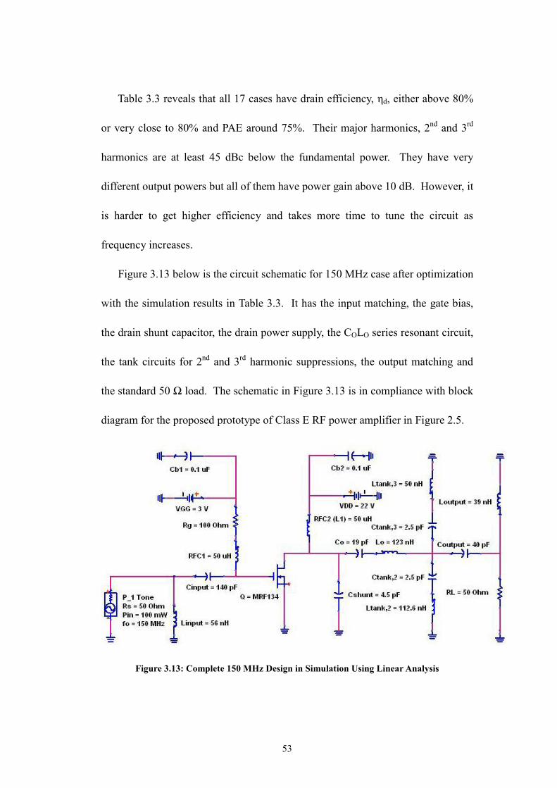
53
Table 3.3 reveals that all 17 cases have drain efficiency, ηd, either above 80%
or very close to 80% and PAE around 75%. Their major harmonics, 2nd and 3rd
harmonics are at least 45 dBc below the fundamental power. They have very
different output powers but all of them have power gain above 10 dB. However, it
is harder to get higher efficiency and takes more time to tune the circuit as
frequency increases.
Figure 3.13 below is the circuit schematic for 150 MHz case after optimization
with the simulation results in Table 3.3. It has the input matching, the gate bias,
the drain shunt capacitor, the drain power supply, the COLO series resonant circuit,
the tank circuits for 2nd and 3rd harmonic suppressions, the output matching and
the standard 50 Ω load. The schematic in Figure 3.13 is in compliance with block
diagram for the proposed prototype of Class E RF power amplifier in Figure 2.5.
Figure 3.13: Complete 150 MHz Design in Simulation Using Linear Analysis

54
Chapter 4: Class E PA Circuit Design Analysis with Nonlinear
Drain Shunt Output Capacitance
The exact drain shunt capacitance is required for Class E RF power amplifiers
to achieve their optimum performances. In Chapter 3, Cshunt is used for this
capacitance, which is composed of both external linear capacitance, Cex,l, and any
output capacitance, Cout, from the transistor. This output capacitance is assumed
to be linear in the analysis and designs in Chapter 3. However, for most FET
transistors, Cout, is nonlinear and it becomes more dominant in Cshunt as operating
frequency increases and eventually it makes up the entire drain shunt capacitance
required for operation. Thus, being able to accurately model the nonlinear
capacitance is important for Class E RF power amplifiers, especially those
operating in high frequencies. In this chapter, the analysis equations for nonlinear
design using MRF134 transistor are derived and the simulation results in ADS for
designs with operating frequencies from 10 MHz to 150 MHz with a 10 MHz
increment are presented for the comparisons with the linear designs in Chapter 3.
4.1 Analysis Equations for Class E Nonlinear Design using MRF134
Chudobiak is the person who derived the first set of design equations
describing the Class E amplifier with a nonlinear shunt capacitance. In his paper
[10], he used 0.5 duty cycle and m = 0.5 for the grading coefficient of the
nonlinear shunt capacitance, which according to his paper is the external drain
shunt capacitance. However, his equations are abstract and inapplicable for

55
practical designs using power MOSFET, such as MRF134 used in this thesis work.
[11] presents an expression for the nonlinear shunt capacitance which uses
data given in most power MOSFET manufacturer’s datasheets, called equivalent
linear shunt capacitance. It also gives a design procedure of a Class E amplifier
with a nonlinear shunt capacitance using the equivalent linear shunt capacitance.
However, the procedure proposed in this paper is based on the assumption that the
output capacitance of the transistor is the only shunt capacitance; there is no linear
external capacitance. It also assumes that the operation has 100% efficiency and
uses 50% duty cycle input signals. In this section, the design equations for the
Class E RF power amplifiers, whose drain shunt capacitance is composed of both
nonlinear Cout and linear Cex,l, by using MRF134 transistor are derived from [11],
and the same assumptions are kept for equation deviations.
Most manufacturers of power MOSFET provide the transistor input, output
and reverse transfer capacitances with the notations Ciss, Coss (the same as Cout in
this thesis), and Crss, respectively, for the specific measurement conditions, usually
VDS = 25 V
VGS = 0 V
fo = 1 MHz
It is important to provide the large signal equivalent circuit of a power
MOSFET for the understanding of the definitions of these three capacitances.
Any practical MOSFET transistor has the following large signal equivalent
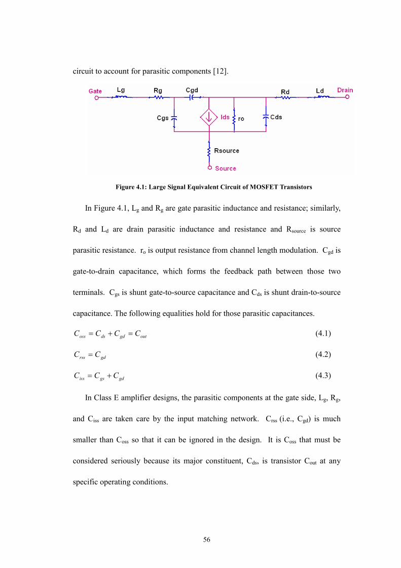
56
circuit to account for parasitic components [12].
Figure 4.1: Large Signal Equivalent Circuit of MOSFET Transistors
In Figure 4.1, Lg and Rg are gate parasitic inductance and resistance; similarly,
Rd and Ld are drain parasitic inductance and resistance and Rsource is source
parasitic resistance. ro is output resistance from channel length modulation. Cgd is
gate-to-drain capacitance, which forms the feedback path between those two
terminals. Cgs is shunt gate-to-source capacitance and Cds is shunt drain-to-source
capacitance. The following equalities hold for those parasitic capacitances.
outgddsoss CCCC =+= (4.1)
gdrss CC = (4.2)
gdgsiss CCC += (4.3)
In Class E amplifier designs, the parasitic components at the gate side, Lg, Rg,
and Ciss are taken care by the input matching network. Crss (i.e., Cgd) is much
smaller than Coss so that it can be ignored in the design. It is Coss that must be
considered seriously because its major constituent, Cds, is transistor Cout at any
specific operating conditions.

57
Transistor MRF134 has 9.7 pF for Coss of, 7 pF for Ciss and 2.3 pF for Crss; all
of them are measured at VDS = 28 V instead of 25 V [8]. Because the drain-to-
source capacitance, Cds, changes with respect to the AC drain-to-source voltage,
Vds, in a nonlinear manner, the design equations for MRF134 are slightly different
from those in [10].
m
bi
s
jods
Vv
CC
)1( += (4.4)
Equation 4.4 is the classic nonlinear drain-to-source parasitic capacitance
derived by Chudobiak [10], in which vs is the DC drain-to-source voltage, same as
VDD used in this thesis; Cjo is the capacitance at zero drain supply voltage; Vbi is
the built-in potential which ranges from 0.5 V to 0.9 V for MOSFET transistors
and m is the grading coefficient of the diode junction, assumed to be 0.5 in [10].
The modified version of Equation 4.4 is below to fit for the measurement
conditions specified in the datasheet of MRF134.
bi
jods
V
CCC
28128
+== (4.5)
The first circuit element that can be obtained is the load resistance, RL, when
using the nonlinear method.
out
DDL P
VR)4(
82
2
+=π
(4.6)
Equation 4.6 calculates the value of load resistance for specified drain DC

58
supply voltage and desired output power. Once RL is known, the linear Cout
required for finding the nonlinear value can be obtained as
Lolinearout Rf
C)4(2
822_ +
=ππ
(4.7)
And the nonlinear output capacitance Cout is
)0239.00061.00781.0(_ DDlinearoutout VCC ++= (4.8)
Equation 4.8 is derived for Vbi = 0.7 V. The linear external capacitance will
then be the difference between the Cshunt from Mr. Sokal’s analysis and Cout in
Equation 4.8 above.
outshuntlex CCC −=, (4.9)
In addition, the value of LO can be found if RL and QL, the loaded quality
factor, are both known.
o
LLO f
QRLπ2
= (4.10)
In Chapter 3, the values of RF chokes are picked randomly as long as they act
as open circuits at fo. In nonlinear analysis, their values are fixed and directly
and inversely proportional to the load resistance and the operating frequency,
respectively.
o
L
fRRFC )1
4(2
2
+=π (4.11)
The equation to find the value CO in the series resonant circuit is simple as in
Equation 4.12.

59
)(21
XQRfC
LLoO −=
π(4.12)
Where, X is the excess reactance in the series LOCO resonant circuit. When LO
and fo are known, X is simply the difference between LO and the inductance
which combing with CO resonates at fo.
))2(
1(2 2Oo
Oo CfLfX
ππ −= (4.13)
Equation 4.13 and 4.14 together can not be used to solve CO. Thus, another
expression for X independent of CO must be known. [11] has a derivation of X
other than Equation 4.13. The results are summarized here.
)tan( 1 ϕϕ −= LRX (4.14)
Where, φ is the phase difference between input and output signals of a Class E
RF PA. It is a constant with the value of -0.567 rad under the assumptions of
100% efficiency and 50% duty cycle operation. φ1 is a complicated expression in
terms of RL, fo, Cjo, and Vbi, which is assumed to be 0.7 V. It is in the unit of
radians.
)325(8)4()2(12]8)4)(486(2[2
tan 222
221
1 −++
++−= −
πππππππ
ϕDDLjobio
DDLjobio
VRCVfVRCVf
(4.15)
The combination 2πfoCjoRL in Equation 4.15 can be found as
bi
DDbiDDDDbibibiLjoo V
VVVVVVVRCf
)4(3)4(9)2424(612
2 2
2242
+
+++−+=
ππππππ
π
(4.16)
Thus, Equation 4.15 simplifies φ1 expression in Equation 4.14 in terms of VDD

60
and Vbi only.
4.2 Circuit Design by Using Nonlinear Analysis
The nonlinear analysis taking account of both nonlinear output capacitance of
the transistor and the linear external drain capacitance is commonly used in the
contemporary designs, especially those operating at frequencies greater than 900
MHz, at which the nonlinear output capacitance is comparable to the linear
external one so that the latter will not be connected in the design at all.
Once the values of supply voltage VDD, the loaded quality factor of series
resonant circuit QL, the operating frequency fo, and the desired output power Pout
are specified for a particular design using MRF134 transistor, the corresponding
circuit component values for RL, RFC, CO, LO and drain shunt capacitances for
both internal nonlinear Cout and external linear Cex,l can be found using the design
equations in the previous section for the assumption Vbi = 0.7 V, 100% efficiency,
i.e., ideal operation, and 50% duty cycle.
Fifteen cases of design with operating frequencies from 10 MHz to 150 MHz
with 10 MHz increment are simulated in ADS using the nonlinear analysis.
Expect their respective fo, all of them have the same operating conditions of VDD =
20 V, VGG = 3 V, Pout = 2.6 W, Pin = 100 mW, QL = 10, and Vbi = 0.7 V. Due to
same values of VDD and Pout, they have same RL according to Equation 4.6. Other
circuit element values are different because of different fo since all other elements,
Cout, Cout_linear, CO, LO and RFC, are all frequency dependent corresponding to
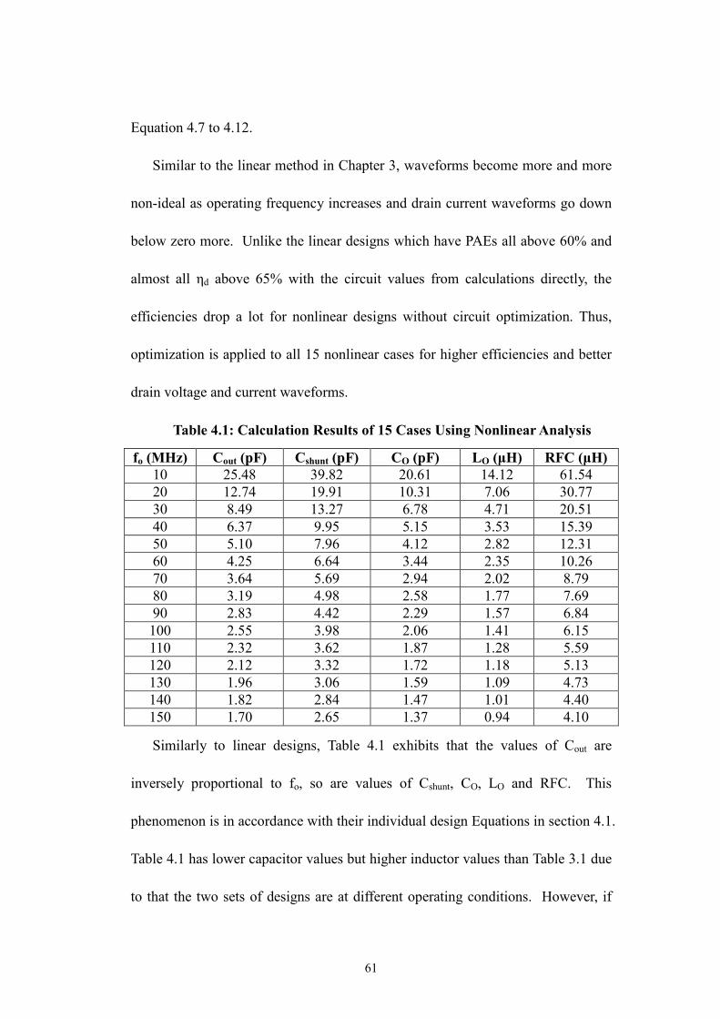
61
Equation 4.7 to 4.12.
Similar to the linear method in Chapter 3, waveforms become more and more
non-ideal as operating frequency increases and drain current waveforms go down
below zero more. Unlike the linear designs which have PAEs all above 60% and
almost all ηd above 65% with the circuit values from calculations directly, the
efficiencies drop a lot for nonlinear designs without circuit optimization. Thus,
optimization is applied to all 15 nonlinear cases for higher efficiencies and better
drain voltage and current waveforms.
Table 4.1: Calculation Results of 15 Cases Using Nonlinear Analysis
fo (MHz) Cout (pF) Cshunt (pF) CO (pF) LO (µH) RFC (µH) 10 25.48 39.82 20.61 14.12 61.54 20 12.74 19.91 10.31 7.06 30.77 30 8.49 13.27 6.78 4.71 20.51 40 6.37 9.95 5.15 3.53 15.39 50 5.10 7.96 4.12 2.82 12.31 60 4.25 6.64 3.44 2.35 10.26 70 3.64 5.69 2.94 2.02 8.79 80 3.19 4.98 2.58 1.77 7.69 90 2.83 4.42 2.29 1.57 6.84 100 2.55 3.98 2.06 1.41 6.15 110 2.32 3.62 1.87 1.28 5.59 120 2.12 3.32 1.72 1.18 5.13 130 1.96 3.06 1.59 1.09 4.73 140 1.82 2.84 1.47 1.01 4.40 150 1.70 2.65 1.37 0.94 4.10
Similarly to linear designs, Table 4.1 exhibits that the values of Cout are
inversely proportional to fo, so are values of Cshunt, CO, LO and RFC. This
phenomenon is in accordance with their individual design Equations in section 4.1.
Table 4.1 has lower capacitor values but higher inductor values than Table 3.1 due
to that the two sets of designs are at different operating conditions. However, if

62
these conditions are kept the same, the same thing also occurs. This can be
verified by plotting in conditions in Matlab codes in Appendix A.4 and A.5 for
circuit value calculations of both analysis methods.
In addition, Table 4.1 shows that the capacitor values are smaller than those
used for the method in Chapter 3 for the same fo, but inductor values are much
bigger. This is caused by the higher QL value in design. In Chapter 3, QL = 5 is
used and it is 10 in the design method of this chapter, which is the lowest
allowable loaded quality factor value for LOCO resonant circuit in order to have a
sinusoidal waveform at the load output with the same frequency as fo for each case.
Higher inductance brings difficulties in circuit implementation and function,
which will be addressed in the next chapter.
4.3 Optimization for 15 Cases by Using Nonlinear Method
The same optimization method as addressed in Chapter 3 is used to increase
the efficiency and improve the waveform shapes for nonlinear designs. Again, it
takes more time to tune the circuit values for higher frequencies. Even though the
efficiencies raise a lot, the waveforms, especially the drain current waveforms,
still differ from the ideal one significantly for high frequencies. They just do not
stay at zero during ON state.
The drain current and voltage waveforms for both 10 MHz and 150 MHz
nonlinear cases after optimization are shown in Figure 4.2 and the complete
simulation results after optimization for all 15 cases are listed in Table 4.2.
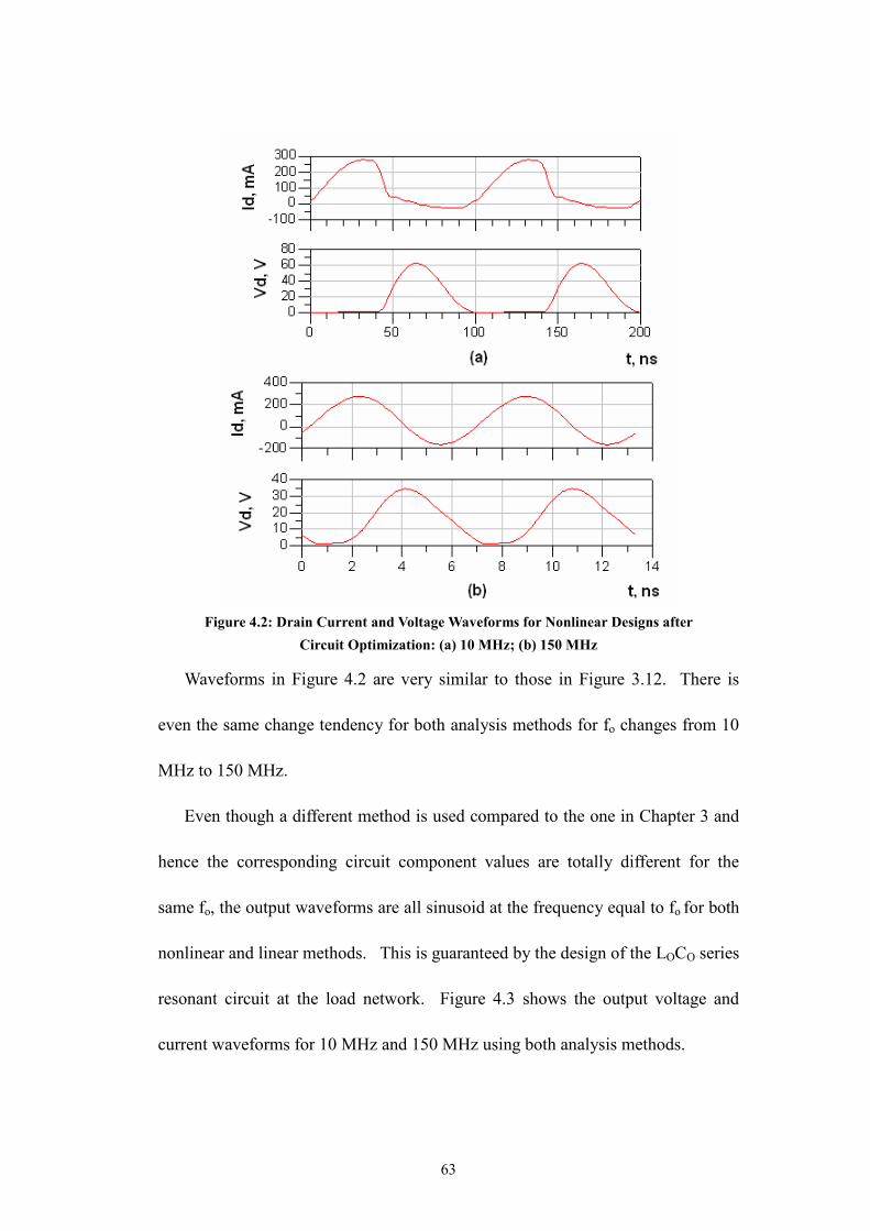
63
Figure 4.2: Drain Current and Voltage Waveforms for Nonlinear Designs after Circuit Optimization: (a) 10 MHz; (b) 150 MHz
Waveforms in Figure 4.2 are very similar to those in Figure 3.12. There is
even the same change tendency for both analysis methods for fo changes from 10
MHz to 150 MHz.
Even though a different method is used compared to the one in Chapter 3 and
hence the corresponding circuit component values are totally different for the
same fo, the output waveforms are all sinusoid at the frequency equal to fo for both
nonlinear and linear methods. This is guaranteed by the design of the LOCO series
resonant circuit at the load network. Figure 4.3 shows the output voltage and
current waveforms for 10 MHz and 150 MHz using both analysis methods.
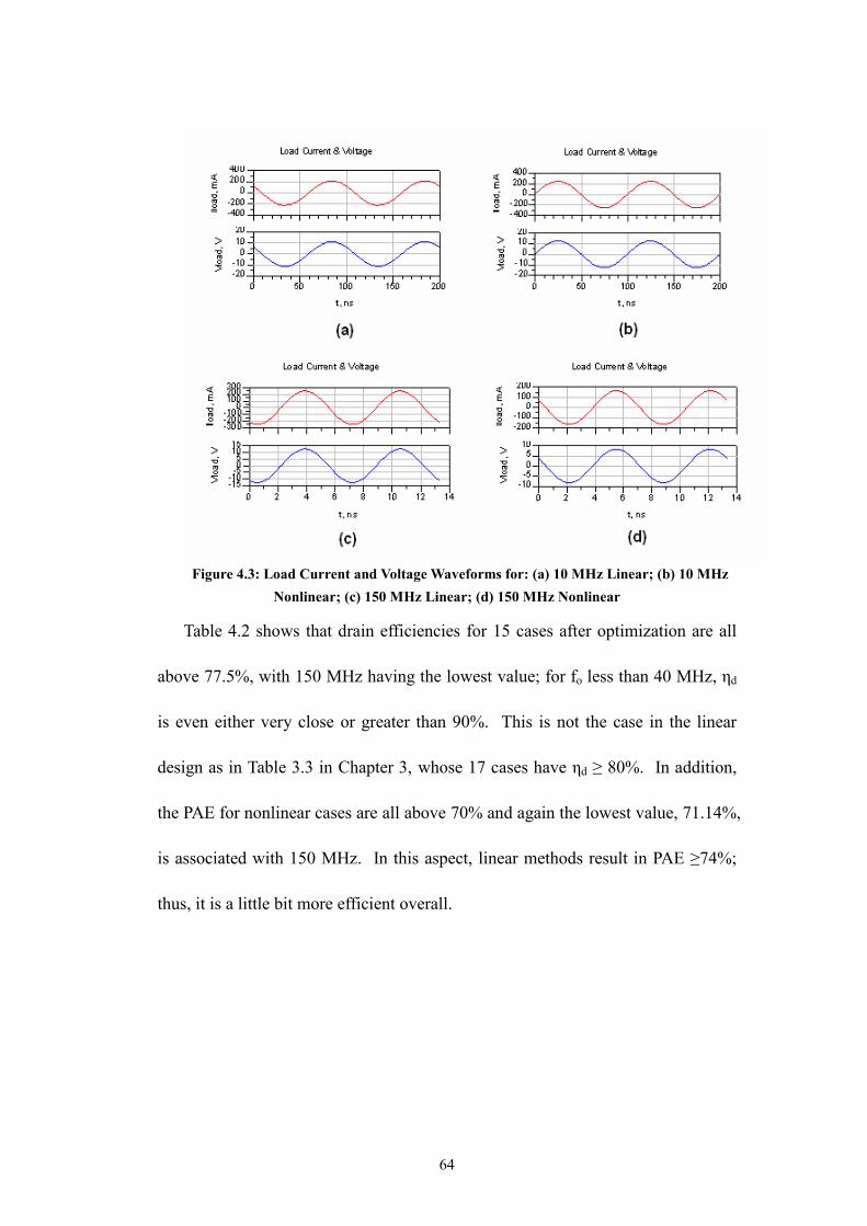
64
Figure 4.3: Load Current and Voltage Waveforms for: (a) 10 MHz Linear; (b) 10 MHz Nonlinear; (c) 150 MHz Linear; (d) 150 MHz Nonlinear
Table 4.2 shows that drain efficiencies for 15 cases after optimization are all
above 77.5%, with 150 MHz having the lowest value; for fo less than 40 MHz, ηd
is even either very close or greater than 90%. This is not the case in the linear
design as in Table 3.3 in Chapter 3, whose 17 cases have ηd ≥ 80%. In addition,
the PAE for nonlinear cases are all above 70% and again the lowest value, 71.14%,
is associated with 150 MHz. In this aspect, linear methods result in PAE ≥74%;
thus, it is a little bit more efficient overall.
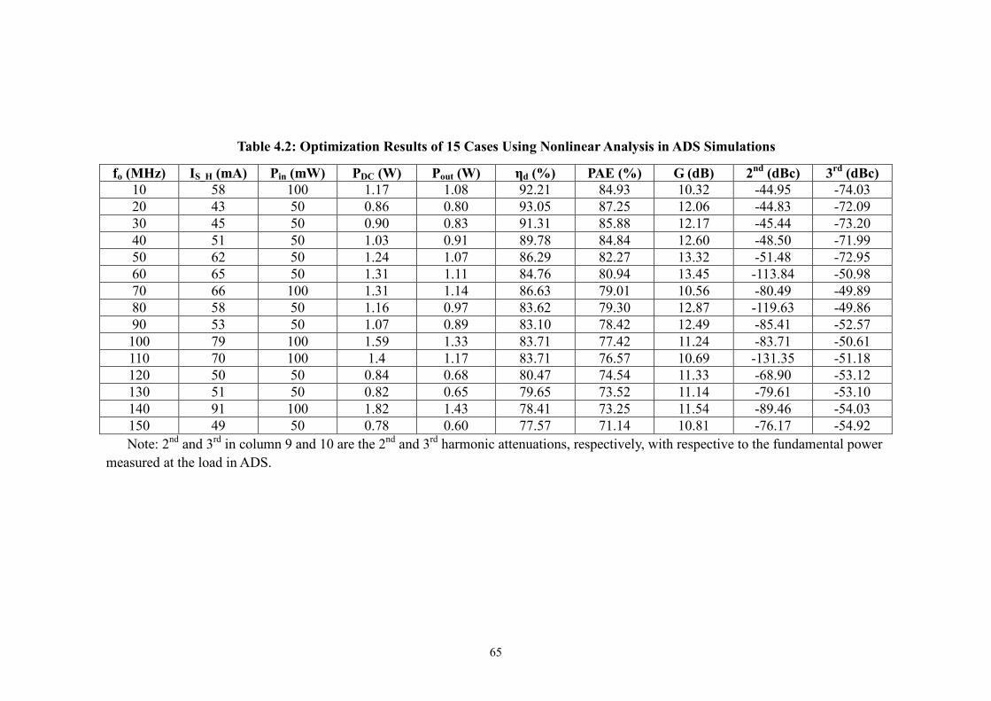
65
Table 4.2: Optimization Results of 15 Cases Using Nonlinear Analysis in ADS Simulations
fo (MHz) IS_H (mA) Pin (mW) PDC (W) Pout (W) ηd (%) PAE (%) G (dB) 2nd (dBc) 3rd (dBc)10 58 100 1.17 1.08 92.21 84.93 10.32 -44.95 -74.0320 43 50 0.86 0.80 93.05 87.25 12.06 -44.83 -72.0930 45 50 0.90 0.83 91.31 85.88 12.17 -45.44 -73.2040 51 50 1.03 0.91 89.78 84.84 12.60 -48.50 -71.9950 62 50 1.24 1.07 86.29 82.27 13.32 -51.48 -72.9560 65 50 1.31 1.11 84.76 80.94 13.45 -113.84 -50.9870 66 100 1.31 1.14 86.63 79.01 10.56 -80.49 -49.8980 58 50 1.16 0.97 83.62 79.30 12.87 -119.63 -49.8690 53 50 1.07 0.89 83.10 78.42 12.49 -85.41 -52.57100 79 100 1.59 1.33 83.71 77.42 11.24 -83.71 -50.61110 70 100 1.4 1.17 83.71 76.57 10.69 -131.35 -51.18120 50 50 0.84 0.68 80.47 74.54 11.33 -68.90 -53.12130 51 50 0.82 0.65 79.65 73.52 11.14 -79.61 -53.10140 91 100 1.82 1.43 78.41 73.25 11.54 -89.46 -54.03150 49 50 0.78 0.60 77.57 71.14 10.81 -76.17 -54.92Note: 2nd and 3rd in column 9 and 10 are the 2nd and 3rd harmonic attenuations, respectively, with respective to the fundamental power
measured at the load in ADS.

66
Chapter 5: Design Implementation and Testing
5.1 Component Selection and PCB Implementation
For the theoretical designs in Chapter 3 and 4, only the transistor model is
fixed, which is MRF134 from Motorola; all other circuit components, such as
inductors, resistors and capacitances, are all ideal one in simulation. For the
actual design at the lab, both resistors and capacitors are 0805 size surface mount
components from Digi-key. Sizes of 0805, 1206, 1008 and 1812 are used for
inductors and only those from CoirCraft are employed. They are from series
0805HQ, 0805 HT, 1008HT, 1008HQ, 1008CS, 1008HS, 1206CS, and 1812FS.
There are three kinds of PCB boards fabricated, Class A, Class E for 10 MHz
and for 150 MHz designs. The layouts are generated in Altium Designer using
Protel software. All of them are two layer boards with signal (i.e. power) layout
on the top and ground layout on the bottom. The sizes for Class A, Class E at 10
MHz and 150 MHz are listed below.
Class A: 3300 mil X 1400 mil (i.e., 3.3 in X 1.4 in)
Class E at 10 MHz: 2500 mil X 1500 mil (i.e., 2.5 in X 1.5 in)
Class E at 150 MHz: 2900 mil X 1600 mil (i.e., 2.9 in X 1.6 in)
The final layouts are shown in Figure 5.1, 5.2 and 5.3.
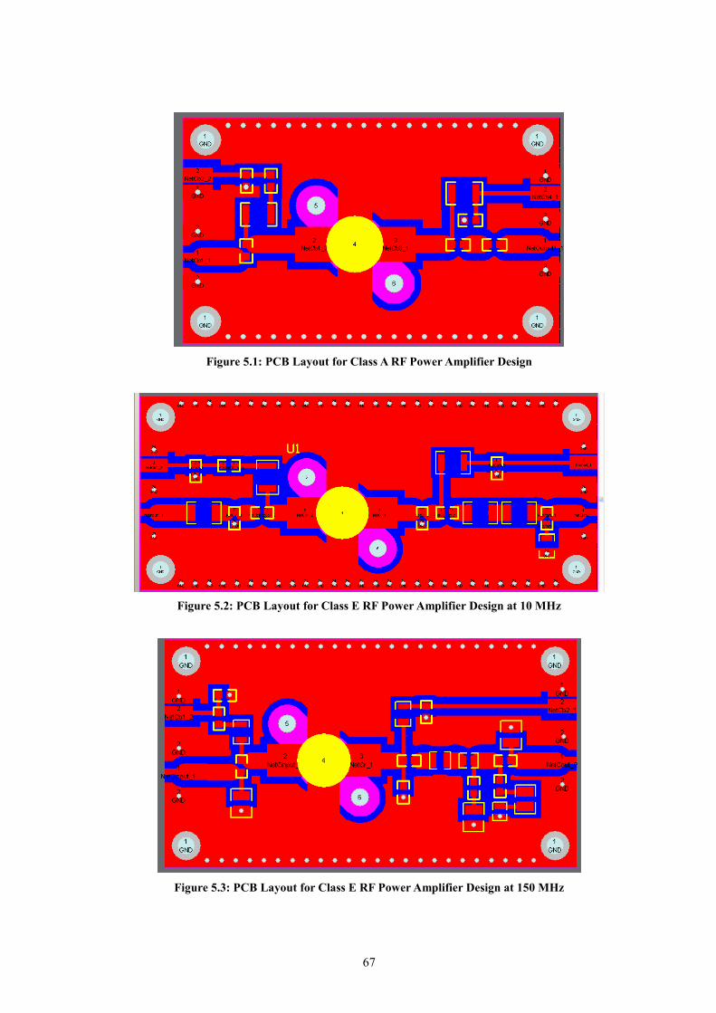
67
Figure 5.1: PCB Layout for Class A RF Power Amplifier Design
Figure 5.2: PCB Layout for Class E RF Power Amplifier Design at 10 MHz
Figure 5.3: PCB Layout for Class E RF Power Amplifier Design at 150 MHz
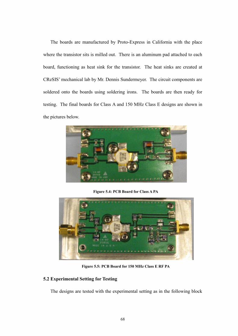
68
The boards are manufactured by Proto-Express in California with the place
where the transistor sits is milled out. There is an aluminum pad attached to each
board, functioning as heat sink for the transistor. The heat sinks are created at
CReSIS’ mechanical lab by Mr. Dennis Sundermeyer. The circuit components are
soldered onto the boards using soldering irons. The boards are then ready for
testing. The final boards for Class A and 150 MHz Class E designs are shown in
the pictures below.
Figure 5.4: PCB Board for Class A PA
Figure 5.5: PCB Board for 150 MHz Class E RF PA
5.2 Experimental Setting for Testing
The designs are tested with the experimental setting as in the following block

69
diagram.
Figure 5.6: Block Diagram of Experimental Setting
The 6060A Synthesized RF Signal Generator is used to output either a 10MHz
or 150 MHz signal with the usable amplitude in the range of 14 dBm to 19 dBm
as the input to a Class A power amplifier, which is solely designed for the usage of
this thesis work because all signal generators at the CReSIS’s lab can provide a
sinusoidal signal no greater than 20 dBm in amplitude. The Class A PA amplifies
the signal, and outputs a new one with the same frequency. Its output range from
200 mW to 500 mW is used as desired input range for the following Class E PA,
which amplifies the signal further. The resultant larger signal is first passed
through a 20 dB 50 Watts power attenuator and then displayed by a signal
oscilloscope, which is a LeCroy Wave Master 8600 A 6 GHz Oscilloscope. The
attenuator is required since all oscilloscopes at the lab can only stand ±4 V peak
to peak signal at 50 Ω coupling. Last, two DC power supplies, Agilent E3630A
Triple Output DC Power Supplies, are employed to support the two power
Signal Generator
Class A PA
Class E PA
DC Power Supply
Power Attenuator
Signal Oscilloscope
DC Power Supply
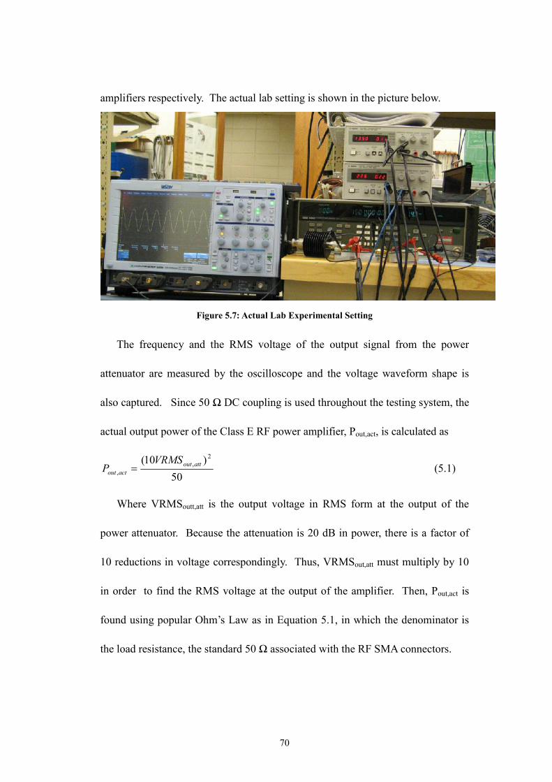
70
amplifiers respectively. The actual lab setting is shown in the picture below.
Figure 5.7: Actual Lab Experimental Setting
The frequency and the RMS voltage of the output signal from the power
attenuator are measured by the oscilloscope and the voltage waveform shape is
also captured. Since 50 Ω DC coupling is used throughout the testing system, the
actual output power of the Class E RF power amplifier, Pout,act, is calculated as
50)10( 2
,,
attoutactout
VRMSP = (5.1)
Where VRMSoutt,att is the output voltage in RMS form at the output of the
power attenuator. Because the attenuation is 20 dB in power, there is a factor of
10 reductions in voltage correspondingly. Thus, VRMSout,att must multiply by 10
in order to find the RMS voltage at the output of the amplifier. Then, Pout,act is
found using popular Ohm’s Law as in Equation 5.1, in which the denominator is
the load resistance, the standard 50 Ω associated with the RF SMA connectors.

71
5.3 Initial Testing
Initially, Class A PA is not used in the testing so that the signal generator
provides the input to the Class E PA directly. Class E PA at 10 MHz and 150 MHz
both using linear and the latter one using nonlinear are tested. The theoretical
designs require 100 mW (20 dBm) for both 10 MHz linear and nonlinear cases
and 50 mW (17 dBm) for 150 MHz nonlinear design. However, the signal
generator used can only output signals with amplitude up to 19 dBm. Thus, it is
used instead of 20 dBm. The testing conditions for each design and the results
are summarized in Table 5.1 and 5.2.
Table 5.1: Initial Testing Conditions
Design Type
Input Power (dBm)
Gate Bias (V)
Drain Supply (V)
10 MHz Linear
20 3 15
150 MHz Linear
20 3 22
150 MHz Nonlinear
17 3 20
Table 5.2: Measurements and Results of Initial Testing
Design Type
Output Frequency
(MHz)
MeasuredID
(mA)
VRMSout,att (V)
Pout,att (W)
Drain Efficiency
(%) 10 MHz Linear
10 60 0.408 0.333 37
150 MHz Linear
150 115 0.616 0.759 30
150 MHz Nonlinear
150 93 0.540 0.583 31.34
The initial testing results are way different from those theoretical values in
Chapter 3 and 4. Not only the output power is much smaller, the drain efficiency
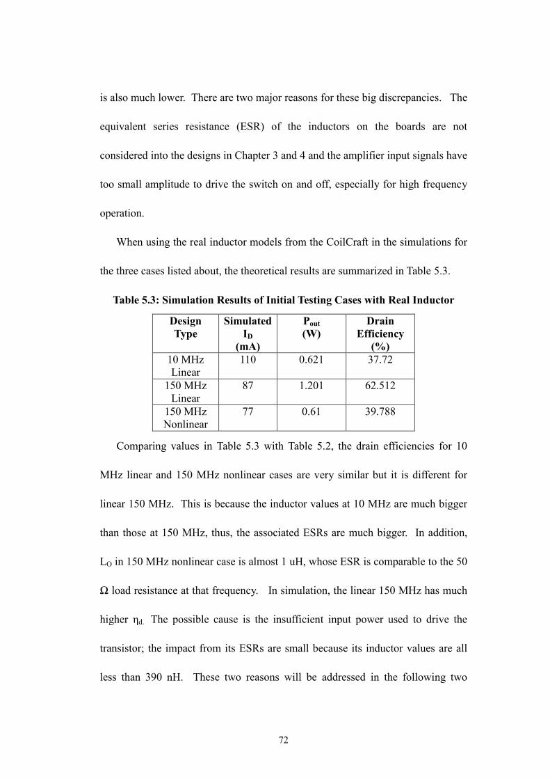
72
is also much lower. There are two major reasons for these big discrepancies. The
equivalent series resistance (ESR) of the inductors on the boards are not
considered into the designs in Chapter 3 and 4 and the amplifier input signals have
too small amplitude to drive the switch on and off, especially for high frequency
operation.
When using the real inductor models from the CoilCraft in the simulations for
the three cases listed about, the theoretical results are summarized in Table 5.3.
Table 5.3: Simulation Results of Initial Testing Cases with Real Inductor
Design Type
SimulatedID
(mA)
Pout (W)
Drain Efficiency
(%) 10 MHz Linear
110 0.621 37.72
150 MHz Linear
87 1.201 62.512
150 MHz Nonlinear
77 0.61 39.788
Comparing values in Table 5.3 with Table 5.2, the drain efficiencies for 10
MHz linear and 150 MHz nonlinear cases are very similar but it is different for
linear 150 MHz. This is because the inductor values at 10 MHz are much bigger
than those at 150 MHz, thus, the associated ESRs are much bigger. In addition,
LO in 150 MHz nonlinear case is almost 1 uH, whose ESR is comparable to the 50
Ω load resistance at that frequency. In simulation, the linear 150 MHz has much
higher ηd. The possible cause is the insufficient input power used to drive the
transistor; the impact from its ESRs are small because its inductor values are all
less than 390 nH. These two reasons will be addressed in the following two

73
sections.
5.4 ESR of Inductors and Its Significance in Class E RF PA Designs
Most manufacture’s datasheet of inductors only provides the maximum ESR at
DC, named as DCRmax. In fact,ESR increases as frequency goes up and very
dramatically for high inductance and it is at its minimum value at DC. ADS is
able to simulate the frequency-dependant behavior of Coilcraft RF surface mount
inductors from 1 MHz to the upper frequency limit specified on the datasheet by
using the lumped-element (SPICE) models provided by Coilcraft.
There are two kinds of lumped-element models for the inductors used on the
designs. Among the inductor series mentioned in section 5.1, the 1812FS series
has a different model than all other ones. Figure 5.8 and 5.9 show the model
schematics [13] and [14].
Figure 5.8: Lumped-Element Models of CoilCraft RF Inductors for Series other than 1812FS, 0805LS, 0603LS and 0402AF.

74
Figure 5.9: Lumped-Element Models of CoilCraft RF Inductors with Series 1812FS, 0805LS, 0603LS and 0402AF.
In Figure 5.8 and 5.9, RVAR and RVAR1, RVAR2 are frequency-dependent
resistances related to the skin effect for both models and they are calculated from
fkRVAR = (5.2)
fkRVAR 11 = (5.3)
fkRVAR 22 = (5.4)
In Figure 5.9, LVAR is the frequency-dependent inductance and is calculated
from
)5log(43 fkkkLVAR −= (5.5)
All values of k, k1, k2, k3, k4, k5, R1, R2, C and L, as well as the upper limit
of the operating frequencies for each inductor model are provided by the Coilcraft.
Then, using the schematics in Figure 5.8 and 5.9 and those variables and constants
in ADS, the ESR value for a specific frequency of an actual Coilcraft inductor can
be found by connecting the two open ports each with a 50 Ω terminator and then
plotting the S-parameters on Smith Chart.
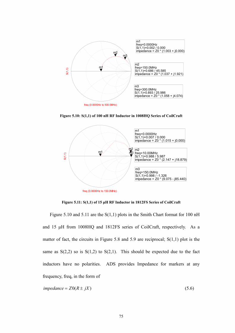
75
freq (0.0000Hz to 500.0MHz)
S(1,
1)m1
m2m3
m1freq=S(1,1)=0.002 / 0.000impedance = Z0 * (1.003 + j0.000)
0.0000Hz
m2freq=S(1,1)=0.686 / 45.585impedance = Z0 * (1.037 + j1.921)
150.0MHz
m3freq=S(1,1)=0.893 / 25.986impedance = Z0 * (1.058 + j4.074)
300.0MHz
Figure 5.10: S(1,1) of 100 nH RF Inductor in 1008HQ Series of CoilCraft
freq (0.0000Hz to 150.0MHz)
S(1
,1) m1
m2m3
m1freq=S(1,1)=0.007 / 0.000impedance = Z0 * (1.015 + j0.000)
0.0000Hz
m2freq=S(1,1)=0.988 / 5.987impedance = Z0 * (2.147 + j18.879)
10.00MHz
m3freq=S(1,1)=0.998 / -1.326impedance = Z0 * (9.075 - j85.440)
150.0MHz
Figure 5.11: S(1,1) of 15 µH RF Inductor in 1812FS Series of CoilCraft
Figure 5.10 and 5.11 are the S(1,1) plots in the Smith Chart format for 100 nH
and 15 µH from 1008HQ and 1812FS series of CoilCraft, respectively. As a
matter of fact, the circuits in Figure 5.8 and 5.9 are reciprocal; S(1,1) plot is the
same as S(2,2) so is S(1,2) to S(2,1). This should be expected due to the fact
inductors have no polarities. ADS provides Impedance for markers at any
frequency, freq, in the form of
)(0 jXRZimpedance ±= (5.6)
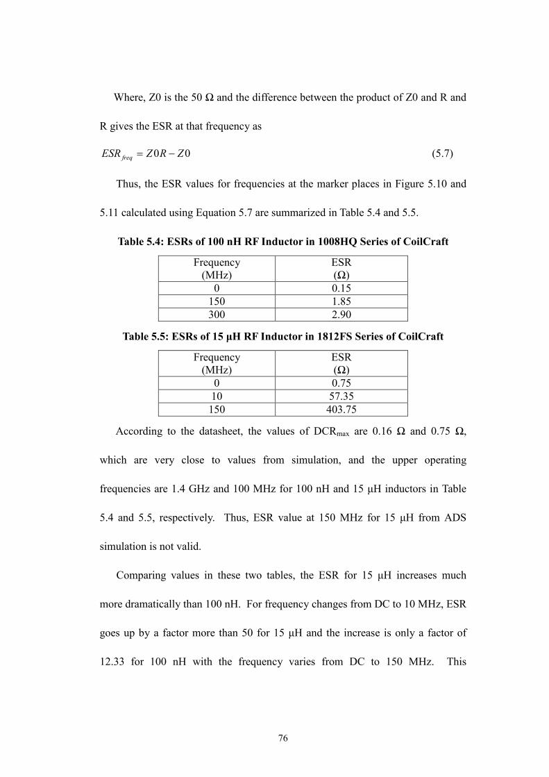
76
Where, Z0 is the 50 Ω and the difference between the product of Z0 and R and
R gives the ESR at that frequency as
00 ZRZESR freq −= (5.7)
Thus, the ESR values for frequencies at the marker places in Figure 5.10 and
5.11 calculated using Equation 5.7 are summarized in Table 5.4 and 5.5.
Table 5.4: ESRs of 100 nH RF Inductor in 1008HQ Series of CoilCraft
Frequency (MHz)
ESR (Ω)
0 0.15 150 1.85 300 2.90
Table 5.5: ESRs of 15 µH RF Inductor in 1812FS Series of CoilCraft
Frequency (MHz)
ESR (Ω)
0 0.75 10 57.35 150 403.75
According to the datasheet, the values of DCRmax are 0.16 Ω and 0.75 Ω,
which are very close to values from simulation, and the upper operating
frequencies are 1.4 GHz and 100 MHz for 100 nH and 15 µH inductors in Table
5.4 and 5.5, respectively. Thus, ESR value at 150 MHz for 15 µH from ADS
simulation is not valid.
Comparing values in these two tables, the ESR for 15 µH increases much
more dramatically than 100 nH. For frequency changes from DC to 10 MHz, ESR
goes up by a factor more than 50 for 15 µH and the increase is only a factor of
12.33 for 100 nH with the frequency varies from DC to 150 MHz. This

77
phenomenon plays a significant role for low frequency designs with high
inductances.
At both 10 MHz linear and nonlinear Class E RF PA designs, inductances
higher than 10 µH are used at the LOCO series resonant circuit and several micro
Henry is needed for the output matching networks. Consequently, there is huge
power dissipation by those ESRs; therefore, the power delivered to the output load
will be reduced considerably, which in turns degrades the efficiencies
exceptionally when the DC power is kept the same.
However, ESRs do not decrease the efficiencies as much for higher frequency
operations such as 150 MHz Class E RF power amplifier design because its
required inductor values are all less than 1 µH. The weak input signal causes the
150 MHz designs have very low efficiencies. The modifications in testing will be
addressed in next section.
5.5 Changes in Testing and New Results
There are two major changes on both circuits and testing setting made. First
of all, the magnitudes of the input signals to the amplifiers are increased from the
initial range 14 dBm-19 dBm to 20 dBm-27 dBm. This boosts the efficiencies by
more than a factor of 2; thus, the drain efficiencies now can reach higher than 60%.
The 6060A Synthesized RF Signal Generator can only output a sinusoidal signal
with magnitude up to 19 dBm. Thus, a Class A PA is used to generate the desired
input signals as in Figure 5.6. Its schematic is shown in Figure 5.12 and its testing
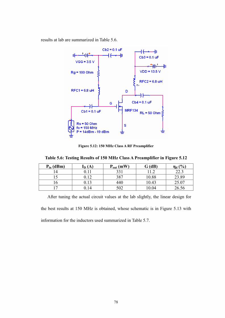
78
results at lab are summarized in Table 5.6.
Figure 5.12: 150 MHz Class A RF Preamplifier
Table 5.6: Testing Results of 150 MHz Class A Preamplifier in Figure 5.12
Pin (dBm) ID (A) Pout (mW) G (dB) ηd (%) 14 0.11 331 11.2 22.3 15 0.12 387 10.88 23.89 16 0.13 440 10.43 25.07 17 0.14 502 10.04 26.56
After tuning the actual circuit values at the lab slightly, the linear design for
the best results at 150 MHz is obtained, whose schematic is in Figure 5.13 with
information for the inductors used summarized in Table 5.7.
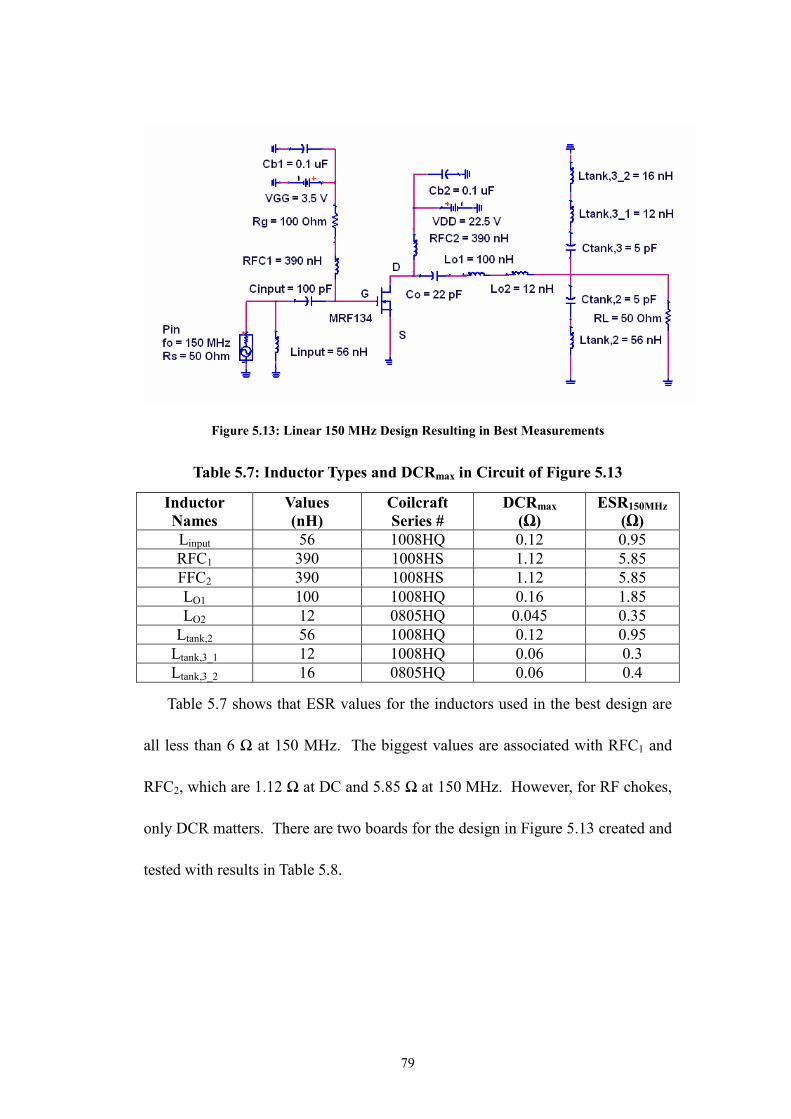
79
Figure 5.13: Linear 150 MHz Design Resulting in Best Measurements
Table 5.7: Inductor Types and DCRmax in Circuit of Figure 5.13
Inductor Names
Values (nH)
Coilcraft Series #
DCRmax (Ω)
ESR150MHz (Ω)
Linput 56 1008HQ 0.12 0.95 RFC1 390 1008HS 1.12 5.85 FFC2 390 1008HS 1.12 5.85 LO1 100 1008HQ 0.16 1.85 LO2 12 0805HQ 0.045 0.35
Ltank,2 56 1008HQ 0.12 0.95 Ltank,3_1 12 1008HQ 0.06 0.3 Ltank,3_2 16 0805HQ 0.06 0.4
Table 5.7 shows that ESR values for the inductors used in the best design are
all less than 6 Ω at 150 MHz. The biggest values are associated with RFC1 and
RFC2, which are 1.12 Ω at DC and 5.85 Ω at 150 MHz. However, for RF chokes,
only DCR matters. There are two boards for the design in Figure 5.13 created and
tested with results in Table 5.8.
80
Table 5.8: Best Testing Results Associated with Design in Figure 5.13
Boards Pin (mW)
ID(A)
VRMSout,att (Vrms)
Pout,act (W)
ηd(%)
G(dB)
S1 440 0.24 1.327 3.522 65.22 9.033 S1 331 0.23 1.300 3.380 65.31 10.091 S3 502 0.22 1.312 3.443 69.55 8.379 S3 331 0.22 1.288 3.318 67.03 10.011
According to Table 5.8, the highest drain efficiency achieved is 69.55% but its
power gain is smaller than other three cases as a tradeoff. The optimum case will
be board S1 which results in a 65.31% of drain efficiency and 10.09 dB of power
gain when 0.331 mW is input from Class A. The simulated results are in Table 5.9
below for comparison.
Table 5.9: Simulation Results of Best Design in Lab
Pin (mW)
ID(A)
Pout (W)
ηd(%)
G(dB)
0.331 0.256 4.119 71.587 10.95 0.440 0.262 4.306 73.029 9.906 0.502 0.265 4.380 73.456 9.407
Comparing Table 5.9 with Table 5.8, the simulation results have higher DC
drain current hence output powers are also higher, so are power gain and drain
efficiencies. The waveforms from both simulation and testing are listed in Figure
5.14 to 5.16.
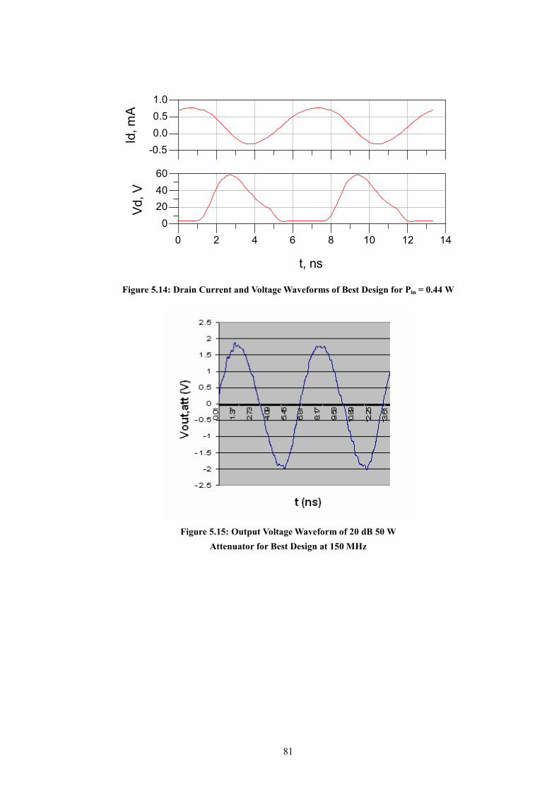
81
0.00.5
-0.5
1.0
Id,m
A
2 4 6 8 10 120 14
2040
0
60
t, ns
Vd,V
Figure 5.14: Drain Current and Voltage Waveforms of Best Design for Pin = 0.44 W
Figure 5.15: Output Voltage Waveform of 20 dB 50 W Attenuator for Best Design at 150 MHz
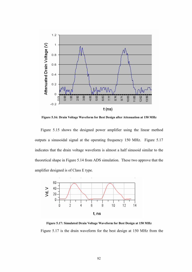
82
Figure 5.16: Drain Voltage Waveform for Best Design after Attenuation at 150 MHz
Figure 5.15 shows the designed power amplifier using the linear method
outputs a sinusoidal signal at the operating frequency 150 MHz. Figure 5.17
indicates that the drain voltage waveform is almost a half sinusoid similar to the
theoretical shape in Figure 5.14 from ADS simulation. These two approve that the
amplifier designed is of Class E type.
Figure 5.17: Simulated Drain Voltage Waveform for Best Design at 150 MHz
Figure 5.17 is the drain waveform for the best design at 150 MHz from the

83
ADS simulation. Its peak value is around 58 V, which is only about 0.97 V in
Figure 5.16. This is because a 30 dB 50 W attenuator is employed for the
measurement. Thus, 0.97 V corresponds to 43.4 V, which is the peak for the drain
waveform of the actual design. The lower peak value is tightly related to the
lower drain DC power due to smaller drain current than theoretical design in ADS.
The efficiencies of 10 MHz linear and nonlinear designs can not be boosted
because no surface mount RF inductors in size of 1812 whose ESR values at 10
MHz are lower than 5 Ω can be found. Similarly, since the nonlinear 150 MHz
design also requires an inductor close to 1 µH for LO in the series resonant circuit,
there is no improvement for the efficiencies and output power. For surface mount
RF inductors from Coilcraft with values close to 1µH, the ESR is more than 15 Ω
at 150 MHz, drawing a significant amount of power which is supposed to go to
the 50 Ω load. For example, the 1µH inductor of 1008HT series has a DCR of 2.8
Ω and ESR of 16.3 Ω at 150 MHz.
5.6 Power Loss Mechanism Analysis
Comparing the simulation results and the measurements for the best design in
Section 5.5, the latter has lower efficiencies, power gain, drain DC current, drain
DC power, and output power. In fact, all these parameters are related in such a
way that for fixed input power of the amplifier, lower DC power will result in
lower output power, which in turns cause lower power gain and efficiencies. Even
with the simulation results, the drain efficiency is only 72.95 %, lower than the

84
initial design in Table 3.3 in Chapter 3, which has only ideal circuit components.
Power loss in the device is causing those differences.
Power loss prevents the efficiency of the amplifier less than 100 % since not
all of DC supply powers as well as the input power are delivered to the load.
There are four major power loss sources associated with Class E amplifiers design.
They are losses from transistor, lumped circuit elements, unwanted harmonics,
and DC power supply path.
5.6.1 Losses from Transistor
The majority part of power loss in a Class E PA design is due to the active
device, i.e., the MRF134 transistor in this thesis work. There are two major loss
mechanisms on the transistor.
a) On Resistance Power Loss (Ron)
Theoretically, the drain current, ID, remains constant with the increase in VDS
during the saturation of a MOSFET, causing the slope of the waveform to be zero
as in Figure 3.5. This rarely happens in practice; in fact, ID changes with VDS in
saturation region, resulting in a constant resistance, which dissipates power when
ID is flowing through it, altering the slope slightly. This is the Channel Length
Modulation of MOSFET transistor addressed in Chapter 3. We call this resistance
as on resistance and denote using Ron.
D
DSon
IVR∆∆
= (5.8)

85
Figure 5.18: Output Capacitance and On Resistance of a MOSFET Transistor
According to Equation 5.8, Ron is infinite in ideal case; thus, it will appear as
an open circuit.
For MRF134 transistor, its DC-IV curves are shown in Figure 3.4, which
indicates that the value of Ron is also very big, hence, the power loss in the device
due to the on resistance is very small and can be neglected.
b) Switching Loss
As frequency increases, the switch behavior will deviate from the ideal one
more and more so that the time needed for switching from NO to OFF state and
vice versa becomes greater. Hence, the transition intervals become longer so that
the drain current and voltage waveforms start smearing out, especially the current
waveform which will change toward a sinusoid with more portion going below
zero. The changes associated with the waveforms will bring power dissipations in
the transistor; therefore, reducing the efficiencies and output power.
Three points in the class E design are aimed to avoid the loss on the transistor:
i) Simultaneous drain voltage and current are avoided
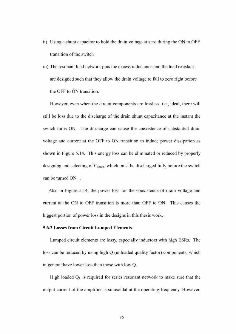
86
ii) Using a shunt capacitor to hold the drain voltage at zero during the ON to OFF
transition of the switch
iii) The resonant load network plus the excess inductance and the load resistant
are designed such that they allow the drain voltage to fall to zero right before
the OFF to ON transition.
However, even when the circuit components are lossless, i.e., ideal, there will
still be loss due to the discharge of the drain shunt capacitance at the instant the
switch turns ON. The discharge can cause the coexistence of substantial drain
voltage and current at the OFF to ON transition to induce power dissipation as
shown in Figure 5.14. This energy loss can be eliminated or reduced by properly
designing and selecting of Cshunt, which must be discharged fully before the switch
can be turned ON. .
Also in Figure 5.14, the power loss for the coexistence of drain voltage and
current at the ON to OFF transition is more than OFF to ON. This causes the
biggest portion of power loss in the designs in this thesis work.
5.6.2 Losses from Circuit Lumped Elements
Lumped circuit elements are lossy, especially inductors with high ESRs. The
loss can be reduced by using high Q (unloaded quality factor) components, which
in general have lower loss than those with low Q.
High loaded QL is required for series resonant network to make sure that the
output current of the amplifier is sinusoidal at the operating frequency. However,

87
the resonant network with a high QL demands a large inductor, which is often not
practical. In addition, large inductor has ESR, which is the winding resistance
resulting from the metal wire forming the coils and frequency-dependent as
addressed in Section 5.4 of this chapter with the problems it causes to the designs.
When current is flowing through the inductor, power is dissipated in the form of
heat by the resistance, inducing a loss of inductive quality. How big this loss will
be for a specific operating frequency, or, how efficient the inductor’s performance
will be, depends on its unloaded quality factor, Q, which is the ratio of inductor’s
reactance at that frequency to its series resistance as
ESRLfQ oπ2
= (5.9)
As revealed by Equation 5.9, for fixed fo and L values, the higher the Q factor
of an inductor is, the smaller ESR value will be and the more efficient the inductor
can perform, and the less loss it will have when current is through and hence, the
closer it approaches the ideal behavior.
In class E operation, even though the series resistance of the inductor in the
series resonant network can be combined into the load resistance, they form a
voltage divider so that the power at the actually load at the output is reduced;
correspondingly, the efficiency is reduced. Furthermore, high QL implies a
smaller 3-dB operation bandwidth for the desired performance as indicated by the
Equation 5.10.

88
BWfQ o
L = (5.10)
Where, BW is the 3-dB bandwidth. Thus, there is a tradeoff between
efficiency and bandwidth.
Even though the best design cases in Section 5.5 have low DCR and ESR
inductors, there are still losses from those parasitic resistances that can not be
eliminated totally, which account as the secondary power loss mechanism
occurring in this thesis work.
5.6.3 Losses from Unwanted Harmonics
In practice, the quality factor (loaded QL) of the series resonant circuit is
below 10. This can not provide sufficient harmonic suppressions, especially for
the attenuation of the 2nd harmonic, which is the largest harmonic in Class E.
Thus, there will be power loss in undesired harmonics if no remedy is made. This
associated loss can be minimized by adding series LC tank circuits, which are
resonant at the desired harmonic frequencies being eliminated, in parallel with the
output load.
The design in this thesis has already included the tank circuit for 2nd and 3rd
harmonic suppressions so that 45 dB attenuation and more are realized for all
harmonics. Thus, there is no loss from this category in the designs having been
done and tested.

89
5.6.4 Losses from DC Power Supply
The actual RF chokes used in this thesis are not ideal at all; they all have non-
zero DCRs. When DC current flows through them, power also is dissipated.
Obvious, the best way to minimize this loss is to use RF chocks with small values
of DCRs. There is a small portion of power loss in this thesis work that is due to
non-zero DCR chokes.

90
Chapter 6: Conclusion
6.1 Conclusion
A Class E RF Power Amplifier prototype is designed and implemented. Two
design methods, linear and nonlinear, are studied and 17 and 15 theoretical design
cases for each method, respectively, with operating frequency up to 150 MHz are
simulated in ADS. All of them have drain efficiencies greater than 77.5%, power-
added efficiencies no less than 71%, and input-output power gain more than 10 dB.
Three cases of design, 10 MHz linear, 150 MHz linear and nonlinear are
implemented at lab using MRF134 transistor from Motorola. Only the 150 MHz
linear design with an actual size 2.9 in X 1.6 in gives the best results, which has
65.31% of drain efficiency and 10.09 dB of power gain with a 0.331 W input
power. In addition, the highest drain efficiency observed is 69.55% with the same
design when 0.502 W of power is input. The measurements are close to
simulation results except the DC drain current observed is lower, which brings in
lower ηd, PDC, Pout and G. The other two designs do not realize desired
performance and the possible reasons are explained.
In conclusion, the Class E RF power amplifier prototype designed and
implemented is functioning desirably and has met the design purposes: small size
but high efficiency.
6.2 Future Work
The prototype has been tested extensively in the laboratory with a preceding

91
Class A power amplifier but still requires testing with other RF devices both
preceding and following it, such as another power amplifier or filters, to check
how it will function when used inside a system.
It should be noticed that the coexistence of the substantial drain voltage and
current at the ON to OFF transition as described in Chapter 5 dissipates the most
power in the transistor, resulting in the biggest power loss mechanism on this
thesis work. The possible causes for this coexistence have not been found and
there are few articles addressing this problem currently. In addition, as frequency
increases, the drain current waveform goes blow zero level, and the negative
current portion becomes bigger and bigger as fo goes up more and more. Also,
there is no work done to explain this phenomenon. The assumption that it is one
property associated with Class E RF power amplifiers has been made in this thesis
but no verification has been given. In the future, efforts must be devoted to solve
these two questions.

92
Bibliography
[1] Jeon, Sanggeun, Design and stability analysis techniques for switching-mode
nonlinear circuits: power amplifiers and oscillators, Ph.D. Dissertation,
California Institute of Technology, 2006.
[2] Sedra, S. Adel and Smith, C. Kenneth, Microelectronic Circuits 4th ed.,
Oxford University Press, Oxford, NY, 1998.
[3] F. Rabb, P. Asbeck, S. Cripps, P. Kenington, Z. Popovich, N. Pothecary,
J. Sevic, and N. Sokal, RF and microwave power amplifier and transmitter
technologies – part 2, High Frequency Electronics, May 2003.
[4] Sokal, Nathan, Class E RF power amplifiers, QEX, pp. 9-20, Jan/Feb 2001.
[5] Tsai, King-Chun and Gray, R. Paul, A 1.9GHz 1W CMOS class E power
amplifier for wireless communications, Department of Electrical Engineering
and Computer Science, The University of California, Berkeley, 1999.
[6] Raab, H. Frederick, Suboptimum operation of class-E RF power amplifiers, in
Proc. RF Technology Expo ’89, Santa Clara, CA, Feb. 14-16, 1989, pp. 85-98.
[7] Brown, Louis, Fundamentals of RF power amplifier design, in CReSIS
Presentation, The University of Kansas, Lawrence, KS, June, 2005.
[8] http://download.siliconexpert.com/pdfs/transistor/mot/mrf134.pdf
[9] Albulet, Mihai, RF Power Amplifier, Scitech Pub Inc, Raleigh, NC, 2001.
[10] Chudobiak, MJ, The use of parasitic nonlinear capacitors in class E
amplifiers, IEEE Trans. Circuits Syst I, Fundam. Theory Appl, vol. 41, no.12,

93
pp.941-944, Dec. 1994.
[11] Suetsugu, Tadashi and Kazimierczuk, K. Marian, Comparison of Class-E
amplifier with nonlinear and linear shunt capacitance, IEEE Trans. Circuits
Syst I, Fundam. Theory Appl, vol. 50, no.8, pp.1089-1097, Aug. 2003.
[12] C. Fager, J.C. Pedro, N.B. de Carvalho and H. Zirath, Prediction of IMD in
LDMOS transistor amplifiers using a new large-signal model, IEEE Trans.
Micro Theory Tech, vol.50, no.12, pp.2834-2842, Dec. 2002.
[13] http://www.coilcraft.com/pdfs/spice_1008ht.pdf
[14] http://www.coilcraft.com/pdfs/spice_1812fs.pdf
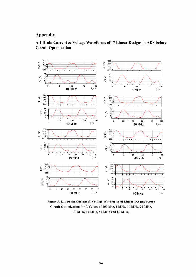
94
Appendix A.1 Drain Current & Voltage Waveforms of 17 Linear Designs in ADS before Circuit Optimization
Figure A.1.1: Drain Current & Voltage Waveforms of Linear Designs before Circuit Optimization for fo Values of 100 kHz, 1 MHz, 10 MHz, 20 MHz,
30 MHz, 40 MHz, 50 MHz and 60 MHz.
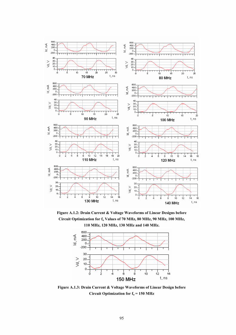
95
Figure A.1.2: Drain Current & Voltage Waveforms of Linear Designs before Circuit Optimization for fo Values of 70 MHz, 80 MHz, 90 MHz, 100 MHz,
110 MHz, 120 MHz, 130 MHz and 140 MHz.
Figure A.1.3: Drain Current & Voltage Waveforms of Linear Design before Circuit Optimization for fo = 150 MHz
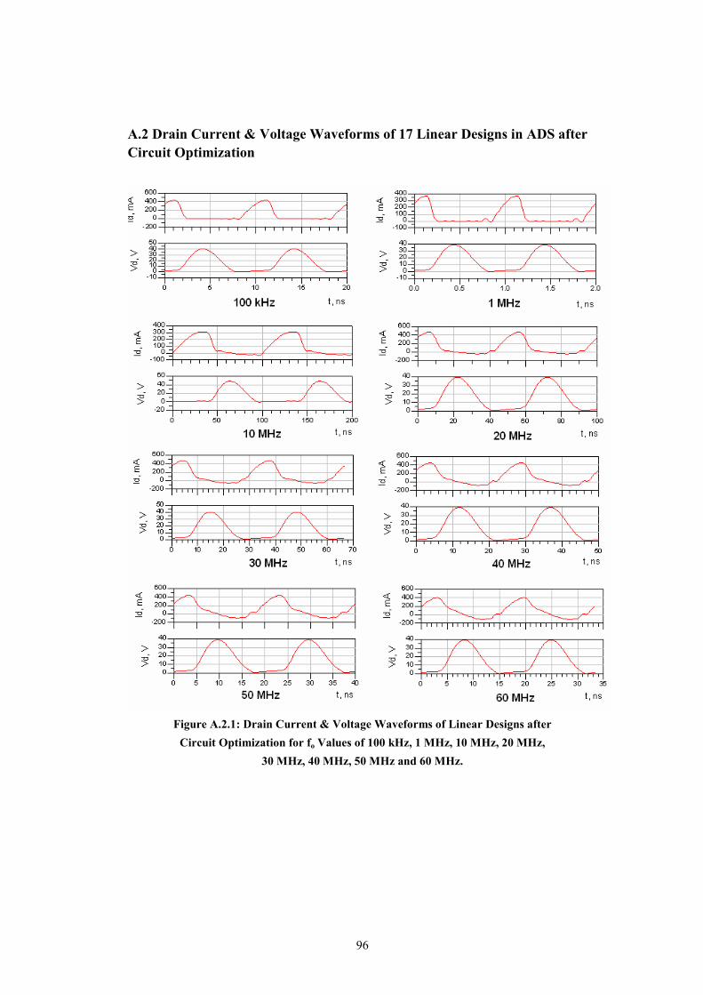
96
A.2 Drain Current & Voltage Waveforms of 17 Linear Designs in ADS after Circuit Optimization
Figure A.2.1: Drain Current & Voltage Waveforms of Linear Designs after Circuit Optimization for fo Values of 100 kHz, 1 MHz, 10 MHz, 20 MHz,
30 MHz, 40 MHz, 50 MHz and 60 MHz.
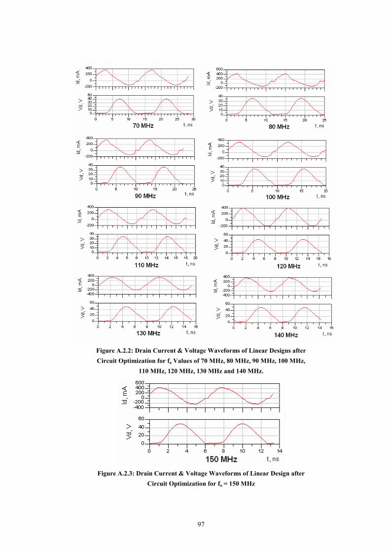
97
Figure A.2.2: Drain Current & Voltage Waveforms of Linear Designs after Circuit Optimization for fo Values of 70 MHz, 80 MHz, 90 MHz, 100 MHz,
110 MHz, 120 MHz, 130 MHz and 140 MHz.
Figure A.2.3: Drain Current & Voltage Waveforms of Linear Design after Circuit Optimization for fo = 150 MHz
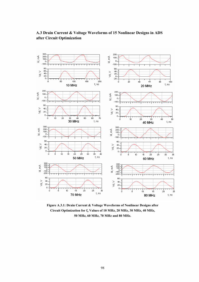
98
A.3 Drain Current & Voltage Waveforms of 15 Nonlinear Designs in ADS after Circuit Optimization
Figure A.3.1: Drain Current & Voltage Waveforms of Nonlinear Designs after Circuit Optimization for fo Values of 10 MHz, 20 MHz, 30 MHz, 40 MHz,
50 MHz, 60 MHz, 70 MHz and 80 MHz.
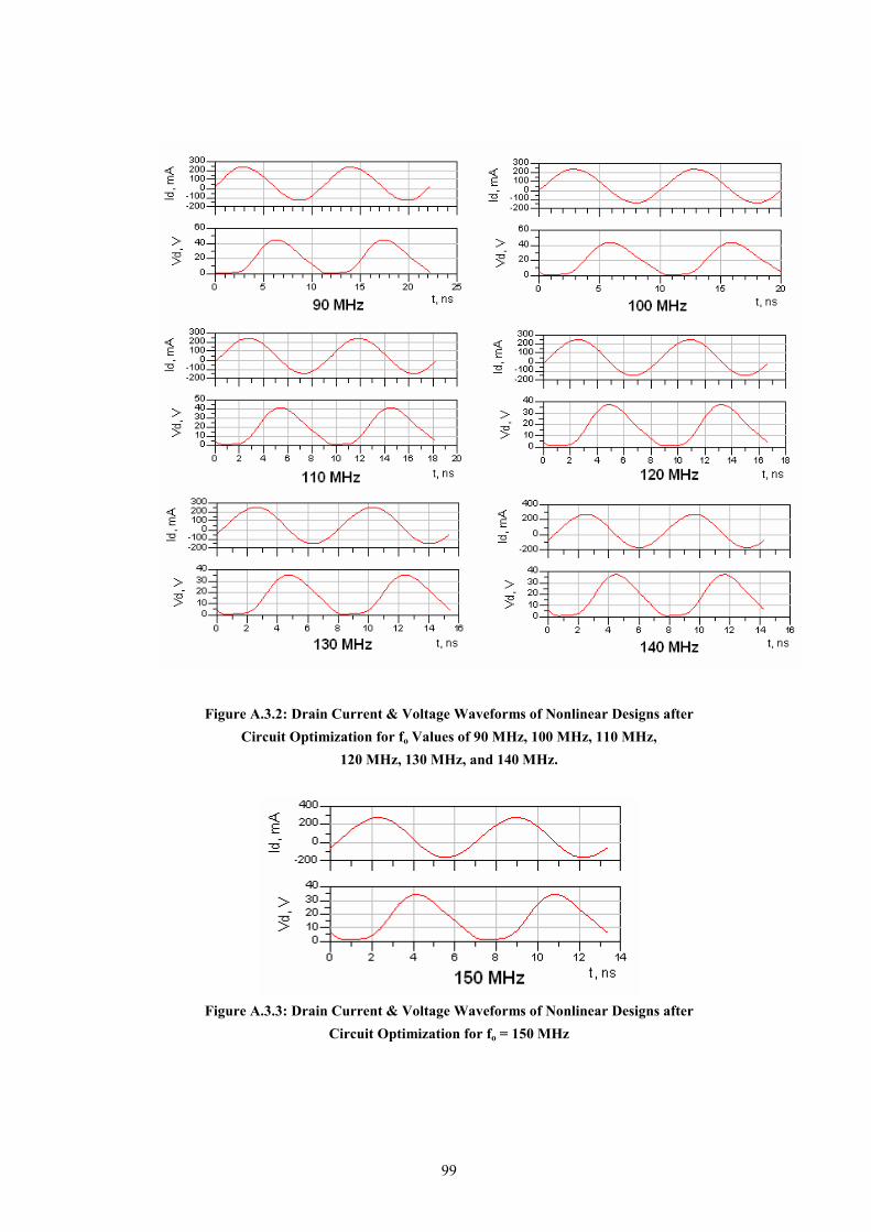
99
Figure A.3.2: Drain Current & Voltage Waveforms of Nonlinear Designs after Circuit Optimization for fo Values of 90 MHz, 100 MHz, 110 MHz,
120 MHz, 130 MHz, and 140 MHz.
Figure A.3.3: Drain Current & Voltage Waveforms of Nonlinear Designs after Circuit Optimization for fo = 150 MHz

100
A.4 Matlab Codes for Circuit Element Calculations Using Linear Method % Spring 2007
clc; clear;
fo= 10e6 % operating frequency in MHz Pout = 5 % desired output power in Watts QL = 5 % loaded quality factor of CoLo series resonant circuit L1 = 18e-6 % L1 is the value for RF chocks used in both gate bias % and drain dc supply, in micro Henry VDD = 15 % drain dc supply voltage in Volts
RL = (VDD^2/Pout)*0.576801*(1.001245-0.451759/QL-0.402444/(QL^2)) % calculate the load resistance Cshunt = (1/(34.2219*fo*RL))*(0.99866+0.91424/QL-1.03175/(QL^2))+0.6/((2*pi*fo)^2*L1) % calculate the drain shunt capacitance Co = (1/(2*pi*fo*RL))*(1/(QL-0.104823))*(1.00121+1.01468/(QL-1.7879))-0.2/((2*pi*fo)^2*L1) % calculate the capacitance in CoLo series resonate circuit Lo = QL*RL/(2*pi*fo) % calculate the inductance in CoLo series resonate circuit

101
A.4 Matlab Codes for Circuit Element Calculations Using Nonlinear Method clc; clear;
fo = 10e6 % operating frequency in MHz VDD = 15 % drain DC supply voltage in V VGG = 3 % gate bias voltage in V Pout = 5 % desired output in Watts QL = 5 % loaded quality factor of CoLo series resonant circuit Vbi = 0.7 % the built-in potential in Volts which typically ranges % from 0.5V to 0.9V Pin = 0.1 % input power in Watts
wo = 2*pi*fo; % operating frequency in radian per second
RL = 8*VDD^2/(pi^2+4)/Pout % calculate the load resistance
C1_linear = 8/(pi*(pi^2+4)*wo*RL) % calculate the linear shunt C,
Cout = (0.0781+sqrt(0.0061+0.0239*VDD))*C1_linear % calculate the % equivalent linear shunt C
woCjoRL_top = 12*Vbi+sqrt(6*Vbi*(24*Vbi-24*pi^2*VDD+pi^4*VDD)+9*pi^2*(pi^2+4)*Vbi*VDD); woCjoRL_bottom = 3*pi*(pi^2+4)*Vbi; woCjoRL = wCjoRL_top/wCjoRL_bottom
IDD = 8*VDD/(pi^2+4)*RL
phi_top = ((6*pi^2-48)*Vbi*woCjoRL+pi*IDD*RL)*2; phi_bottom = 24*pi*Vbi*woCjoRL+(5*pi^2-32)*IDD*RL; phi_aug = phi_top/phi_bottom; phi = atan(phi_aug)
phy = -0.567;
X = RL*tan(phi-phy)
Lo = RL*QL/wo % calculate the inductance in series resonant % circuit

102
Co = 1/(wo*(RL*QL-X)) % calculate the capacitance in series % resonant circuit
RFC = 2*(pi^2/4+1)*RL/fo % calculate RF chocks used in both gate % bias and drain dc supply