design and demultiplexer for satellite applications · 2005-02-12 · this thesis addresses the...
TRANSCRIPT

Design and Implementation of a Group Demultiplexer
for Satellite Applications by
Arati Chandrasekhara, B .Eng, India
A thesis submitted to the Faculty of Graduate Studies and Research
in partial fulfillment of the requirernents for the degree of
Master of Engineering
Ottawa-Carleton hstitute of Elecmcal Engineering Department of Electronics
Faculty of Engineering Carleton University
Ottawa, Ontario, Canada April 1998
@ Copyright 1998

National Library I * m of Canada Bibliothéque nationale du Canada
Acquisitions and Acquisitions et Bibliographie Services services bibliographiques
395 Wellington Street 395. nie Wellington OtîawaON K I A ON4 OttawaON K 1 A W Canada canada
The author has granted a non- exclusive licence allowing the National Library of Canada to reproduce, loan, distriiute or sell copies of this thesis in microform, paper or electronic formats.
The author retains ownership of the copyright in this thesis. Neither the thesis nor substantial extracts fiom it may be printed or otherwise reproduced without the author's permission.
L'auteur a accordé une licence non exclusive permettant à la Bibliothèque nationale du Canada de reproduire, prêter, distribuer ou vendre des copies de cette thèse sous la fome de microfiche/^ de reproduction sur papier ou sur format électronique.
L'auteur conserve la propriété du droit d'auteur qui protège cette thèse. Ni la thèse ni des extraits substantiels de celle-ci ne doivent être imprimés ou autrement reproduits sans son autorisation.

Abstract
Signai regeneration on-board the satellite makes it possible to use different rnulti-
pIe access schemes for the uplink and the downlink. The uplink and the downlink c m be
separately optimized for greater power efficiency and bandwidth utilization. A multiple
access scheme using frequency division multiple access (FDMA) for the uplink and tirne
division multiplex (TDM) for the downlink has been considered for regenerative satellite
communications. This method has been found more efficient and cost efiective as com-
pared to using either FDMA or TDMA for both the uplink and downlink transmission.
The conversion from frequency to time division multiplex format cequires the uplink sis-
na1 to be demultiplexed and each individual carrier to be demodulated.
The demultiplexing part of the process can be performed by a nurnber of different
srmcmres. Arnong those the one that has received the most attention for satellite applica-
tions is the polyphase filter network followed by a fast fourier transform (FFT) processor.
Also, the environment in which the satellite operates necessitates the use of radiation-
hardened technology for on-board processing (OBP) hardware. Where volumes and eco-
nomic factors warrant it, an application specific integrated circuit (ASIC) irnplementation
based on radiation-hardened gate arrays could be the preferred technology. However, in
view of the cost and time constraints associated wit!! such an implementation, it is of inter-
est to consider the viability of implementing OBP hardware on radiation-hardened field
pro~ammable gate arrays (FPGAs).

This thesis addresses the design and implernentation of a polyphase-FFT 8 chan-
nel, Tl rate, group demultiplexer, to test the viability of OBP hardware realization with
radiation-hardened FPGA technology. The design of the group demultiplexer for imple-
mentation on FPGAs with modest gate counts involves identifying suitable architectures
for the building blocks of the group demultiplexer. These architectures allow a trade-off
berween the required number of gates (device utilization) and speed of operation. The
architectures developed ensure that the device utilization is low and that the requirements
of speed are met.
An implementation which has been optimized in terms of speed and device utiliza-
tion is presented in this work. Also, addressed here is the possibility of extension of the
implementation to incorporate larger nurnber of channels. The implernentation presented
here utilizes the largest available radiation-hardened devices from Acte1 (8K gates) and its
non-hardened counterpart (8K gates). Aso. considered here are the implications of the
implementation of the design on larger radiation-hardened devices when they become
available-The practicality of applying FPGA technology to the implementation of OBP
circuits will increase considerably once radiation-hardened FPGAs with a higher gate
equivalence become available.
Acknowledgments
1 would like to thank my supe~isors, Dr. Tad Kwasniewski and Dr. Valek Szwarc.
for their guidance and support throughout my research at Carleton University and Com-
munications Research Centre (CRC).
Carleton University, Canadian Institute for Telecommunications Research ( C m )
and Communications Research Centre (CRC) are ,gateefully acknowledged for providing
the financial support. I thank my colleagues at CRC for their help and suppon.
Finally, to my family and friends: thank you for your love and suppon.

CONTENTS
List of Tables ..................................................................................... List of Figures .....................................................................................
.......................................................................... List of Abbreviatiom
Chapter 1: Introduction
.................................................................................................... 1.1 Background ... . . ............................................................................................. 1.2 Thesis Motivation
............... ............................... 1.3 Thesis Objectives .. ................................................................... 1.4 Thesis Outline ........................
Chapter 2: On-Board Processing Demultiplexer Architectures
2.1 Introduction ....................................................................................................... ......................................................................................... 2 2 Per-Channel Method
.................................................................................................... 2.3 B lock Method 2.3.1 The F F T m Frequency Domain Filtering Approach .........................
......................................................................................... 2-32 Polyphase-FFT ............................................................................................ 2.1 Multistage Method
2.5 Cornparison of the Demultiplexer Architectures ............................................ 2.6 Conclusion ........................................................................................................
Chapter 3: Polyphase-FFT Demultiplexer
3.1 Introduction ....................................................................................................... ............................................................................ 3 -2 On-Board Receiver Structure
........................ 3 -3 Anal ysis of the Polyphase-FFT Digital Group Demultiplexer 3.3.1 The Input FDMA Signals ........................................................................ 3.3.2 The Polyphase-FFT Network .............. ..... ......................................... 3.3.3 Interpolation in the Channel Rocessor for Rate Conversion ....................
...................................................................................... 3.3.4 The Final Output 3 -4 Conclusion ............ ..... .................................................................................

Chapter 4: Actel FPGA Technology. CAD Tools. Design and Test Environment
4.1 Introduction ....................................................................................................... ... .................................................... 4.3 Acte1 Antifuse FPGA Technolo gy ......,.....
4.2.1 Actel Device Architecture ........................................................................ 4.3.2 Acte1 FPGA Families and Macro Library ... .............................................. 4.2.3 Radiation-Hardened FPGAs ............................. ..-. ..... 3.2.4 RH1280 and A 1380XL device fearures ................................................... 4.2.5 Acte1 FPGA CAD Tools ....................................... ... ......................
........................................ 4.2.6 Actel FPGA Design Cycle ... .............................................. ...... 1.3 Mentor Graphics Design Environment .....
3.4 Conclusion .............. .... ......................................................................................
Chapter 5: Polyphase-FFT Group Demultiplexer System Architecture
5.1 Introduction ...................................................................................................... 5.2 Building Blocks and Architecture of the Polyphase-FFT Group
............................................................................... Demultiplexer ........ ...... ...................................... 5.3 S y stem Specifications and Parameters ........... .......
............... ................................. 5.4 Interfacing between the Building Blocks .... ............................................................................................. 5.5 Clocking Scheme
5.6 Timing Inf~rmation ........................................................................................... 5 -7 Conclusion ........................................................................................................
Chapter 6: Polyphase-FFT Group Demultiplexer Implementation
...................................................................................................... Introduction ........... ............................*........................-.-* Polyphase Filter Network .......
.................................... 6.2.1 Filter Coefficients for the Polyphase Network ........................................... 6.2.2 Implementation of the Polyphase Subfilters
6.2.3 Cornparison of Different Architectures for the Implementation of the Polyphase Subhlters .................................................................................
.................................................................................................. Phase Shifters 6.3.1 Implementation of the Phase Shiften ..................... .. ............................
6.4 Irnplementation Results for the Polyphase Subfilten and the Phase S hifiers .................................................................................................. 82
vii

........................................................................... Fast Fourier Transform (FFT) ....................................... ................. 6.5.1 Decimation in Time (DIT) ..
.................................. .................................. 6.5.2 FFï Irnplementation ... 6.5.3 FFï Irnplementation Results ................................................................. Rate Conversion Filter ..................................................................................... 6.6.1 Rate Conversion Filter Coefficients ...................................................
......................................... 6 . 6 2 Implementation of the Rate Conversion Filter 6.6.3 Rate Conversion Filter Implementation Results ......................................
6.7 Conclusion ........................................................................................................
Chapter 7: Summary and Suggested Further Research and Development
7.1 Further Research and Development .............................................................. 107
References ......................................................................................... 109
............................................................ ..................... Appendix A .. 112 Timing Data
.......................................................................................... Appendix B 115 List of Coefficients for Polyphase and Rate Conversion Filten and Phase Shift Multipliers
....................................................................................... Appendiv C 118 Raised-Cosine Fiiter

List of Tables
................................................ Table 4-1: Characteristics of Actel FPGA famiiies ............................................ Table 4.2: Radiation-hardened target specifications
............................... Table 4.3: Features of Actel RH1 280 and A l28OXL devices Table 4.4: Specifications for the operating conditions (commercial applications)
............. Table 5.1 : System parameters of the implemented group demultiplexer Table 5.2: Pararneters for the building blocks of the implemented group
dernultiplexer ............... .... ................................................................ .............................. Table 4.3: Perrnissible interconnect delays between devices
.................................. Table 6.1 : Parameters for the polyphase filters ............,.... Table 6.2a: Device utilization and delay for two subfilters (real and quadrature)
with the phase shifter for that channel for channels 1,2, 3 and 4 ............ Table 6.2b: Device utilization and delay for two subfilters (real and quadrature)
Table 6.3:
Table 6.4: Table 6.5:
Table A l : Table A2:
Table A3:
Table B 1 : Table B2: Table B3:
........... with the phase shifier for that channel for channels 5.6.7 and 8 Device utilization and delay for the 8.poin t. 12 bits input/output (complex) DIT- FXT...............................................................................
................... ....................... Parameters for the rate conversion filters .... Timing and device utilization for the two rate conversion filters
............................................... (real and quadrature) on a single device Timing information for the input and output for the devices pl to p8 .. Timing information for the input and output for the FFT devices
................................................. ........................ fla, flb, fZ and f3 ... Timing information for the input and output for the eight devices
.......................................... ............. of the rate conversion filters ..... ..................................................... Coefficients for the polyphase filter
......................................................... List of phase shifter multipliers ................ ................ Coefficients for the rate conversion filter ....

List of Figures
F i e 1 : Block diaCam of group demodulator ................................................. ................. Figure 2.1 : "Per-Channel'' demultiplexer (Analytic signal approach)
Figure 2.2. Frequency demultiplexing in the AS method ................................... .............. Figure 2.3: FFTAFFI' fiequency domain filtering method for channel k
Fi,= e 2.4. "B lock" dernultiplexer (pol p h a s e - F m ............................................ Fi,w e 2.5. "Multistage" demultiplexer (4 channels) ........................................... F r 2.6 Multistage spec tra. ...........................................................................
........................ Figure 3.1 : Frequency spectrum of the transmitted FDMA signal Figure 3.2a. On-board receiver smcture ................................................................
.................. .... Figure 3.2b. Frequency spectrum at points A B ,C,D.O. 1 -W- 1 ...... Figure 3 -3: Baseband mode1 for N=8 channels as input to the demultiplexer ....... Figure 3.4. Mode1 for demultiplexing of a single channel ....................................
... F r 3 . 5 Polyphase network, FFT processor used to demultiplex N channel Figure 3.6: Timing relationship between input and output sarnples in the
rate conversion filter ......................................................................... F r 4 . 1 : Basic Acte1 FPGA architecture ....................................................... Figure 4.2: Standard flow for FPGA design based on the Actel and
Mentor Graphics tools ........................................................................ F r 5.1 : Polyphase-FFT demultiplexer with rate conversion filten ................. Figure 5.2. BER vs . SNR curve for the irnplemented poup dernultiplexer ....... Figure 5.3: Interfacing between the 12 devices used in the implementation of
the polyphase-FFï demultiplexer ....................................................... Fipre 5.4: Timing relationship between the clocks for the 8 channels for the
polyphase subfilters .................. ... ................................................... Figure 5.5. Input and output delays ............. .. ....................................................
............................................. Figure 6.1 : Decomposition of hRcv4in) with N=4 ........................ Figure 6.2. Direct form realization for filter for channei 1. ........ ..
Figure 6.3. Block diagram for the implementation of the polyphase subfilters .... Figure 6.4. Binary fractional fixed format representation ..................................... Figure 6.5. Block d i a m for the 8 point radix-2 DIT FFT ............................... Figure 6.6. Eight point DIT FFï algorithm ........................................................... Figure 6.7. Complex butterfly for DIT FFï .................................................... Figure 6.8. Flow diagram of the 8 point DIT FFT'.................. .... ................... Figure 6.9. Implementation of the radix-2 . 8 point DIT FFI .............................

Figure 6.10. Device partitioning for the FFT ................................... ..... ................... 96 Figure 6.1 1 : Direct form realization of the rate conversion filter ............................ 101 Figure 6.12. Block diagram for the irnplementation of the rate conversion filter .... 102 Fi,w e C . 1 : Frequency response of raised-cosine filter for different roll-off
factors ................................................................................................ 119 Figure C.2: Impulse response of raised-cosine filter for different roll-off factors .. 1 19

List of Abbreviations
AS -4SIC c m CITR CLB CMOS CRC CSA DEMOD DEMUX DIT DSP EPROM EEPROM FDM FDMA FFT F R FPGA GaAS HPA I/O n=Fr MCD MCDD 1MCM OBP O N 0 PLICE QPSK RAM RF SAW SCPC
Anaiytic Signal Application Specific Integrated Circuit Computer Aided Design Canadian Institute for Telecomrnunications Research Confi,wable Logic B lock Complementary Metal Oxide Semiconductor Communication Research Centre Carry Save Adder Demodulation Demul tiplexing Decimation-in-Tirne Digital Signai Processing Electrically Programmable Read Only .Mernory Electricall y Erasable Programmable Read On1 y Memory Frequency Division Multiplex Frequency Division Multiple Access Fast Fourier Transform Finite Impulse Response Field Programmable Gate Array Gallium Arsenide High Power Amplifier Input/Output Inverse Fast Fourier Trans form Multicmier Demodulation Multicarrier Demultiplexer Demodulation Multi-Chip Module On-B oard Rocessing Oxide-Nitride-Oxide Programmable Low Impedance Circuit Element Quadrature Phase S hift Key ing Random Access Memory Radio Frequency Surface Acoustic Wave Single Channel Per Carrier
xii

Si SOS SRAM SSB TDM TDMA -lMux TTL TWTA VHDL a s 1
Silicon Silicon On Sapphire Static Random Access Memory Single SideBand Time Division Multiplex Time Division Multiple Access Transmul tiplexer Transistor Transistor Logic Travelling Wave Tube Amplifier Very High Speed Integrated Circuit Hardware Description Language Very Large Scaie htegration

CHAPTER 1: Introduction
CHAPTER 1
Introduction
1.1 Background
To examine the feasibility of field programmable gate array (FPGA) design. of a
oroup demultiplexer, a representative subsystern which simultaneously demultiplexes 8 C
QPSK channels, each with a cornplex data rate of 0.722 Msamples per second is consid-
ered here. The work presented here is in the framework of the on-going research on on-
board processing (OBP) techniques at Communication Research Centre (CRC) [ l ] and
Canadian Institute for Telecommunications Research ( C m ) . OBP enables signal regen-
eration on board the satellite and makes it possible to use different multiple access

CHAPTER 1: Introduction 2
schemes on the uplink and downlink.
For the OBP system frequency-division multiple access usinj single channel per
carrier (SCPC-FDMA) on the uplink and time-division multiplex (TDM) on the downlink
is assumed. With SCPC-FEMA, each earth station in the satellite network uansmits a
radio frequency (RF') carrier to the satellite transponder. Each uplink carrier occupies a
specific frequency band location within the uplink bandwidth. In addition. the data rate is
typically constant, for al1 channels. so that each station has the sarne bandwidth and the
network is uniform. With TDMA systems, each station transmits one data frame at a time
which is globally synchronïzed in time to avoid collision. For both FDMA and TDMA the
uplink signal is amplified by the satellite's travelling wave tube amplifier V A ) and
retransmitted in the downlink bearn. As compared to the TDMA method, the SCPC-
FDMA method on the uplink reduces the cost and cornplexity of the earth terminais con-
siderably, because global synchronization is not needed. However. amplification of the
multiple carriers by the TWTA operated at saturation on the downlink produces intermod-
dation distortion which significantiy degrades individual channel performance. On the
other hand, with TDMA since there is only one carrier at a time, the intermodulation dis-
tortion is elirninated [2 ] .
The S C P C - F D M m M link combines the advantages of SCPC-FDMA on the
uplink and the bencfits of the TDMA on the downlink. Thus. this method reduces the cost
and complexity of the earth stations and allows the satellite amplifies to operate at satura-

CHAPTER II Introduction 3
tion for maximum efficiency. It enables high power amplifier (HPA) power and antenna
size at the earth terminal to be reduced [3]. Also. splitting of the satellite link into two dis-
tinct sections prevents noise and other interference to be accumulated and msferred from
the uplink to the downlinlr. which irnproves performance.
The above discussions indicate the benefits of using FDMA on the uplink and
TDM on the downlink in satellite communications systems. The FDMAiTDM configura-
tion necessitates on-board signal regeneration in which the FDMA uplinks are frequency
demultiplexed and then the individual c h e r s demodulated routed and recornbined into
TDM sipals for retransmission.
The digital sipal processing (DSP) operation which simultaneously downconverts
multiple FDM sipals to baseband is referred ro as multicarrier demodulation and the
device which accomplishes this is called a multican-ier demodulator (MCD). Multicarrier
demodulation includes frequency demultiplexing of the FDM carriers and subsequent
demodulation of each carrier to recover the individual channel data Figure 1.1 depicts the
block diagram for a group demodulator. It consists of two main blocks: a digital group
demultiplexer and a bank of channel processon. The digital group demultiplexer separates
out the individual channels in the received signal. The hnction of the channe1 processors
is then to regenerate each signal by performing timing and carrier recovery and making
decisions on the QPSK signal.
Several digital approaches to demultiplexing have been proposed. A very good


CHAPTER I: Introduction 5
description of digital methods to convert FDM to TDM and vice-versa (transmultiplexing
methods) is available in [4]. Of the various transmultiplexing designs the one that has
received the most attention for on-board processing consisü of a digital polyphase net-
work followed by an FFT processor. The basic structure of the digital transmultiplexer on
which the poup demultiplexer is based was first proposed by Bellanger [5]. The structure
proposed by Bellanger was aimed at telecornmunication networks. for direct translation
from TDM to FDM format or vice-versa. The fint polyphase-FFT structure for on-board
processing was proposed by Takahata et al. 131.
Several authors have also considered a demultiplexer design based on a series of
half-band filters arranged in a binary tree. This multistage demultiplexer was first pro-
posed by Tsuda et al. [6] for use in switched telephone networks. Gockler and Eyssele [7]
have provided a design that is suited for on-board processing.
The frequency domain approach [8], [9] is another method for performing demulti-
plexing. This method becomes attractive for configurations with large number of channels
with carriers of different bit-rates and bandwidth requirements. Another approach. the per-
channel method [IO], [ 1 11, [12], performs the dernultiplexing operation by individual
bandpass filters, each assigned to an SCPC channel.
The high-speed, low-power and high levels of integration required determines the
technologies which cm be used for on-board processors. Furthemore, the space environ-
ment in which these devices operate dictates the use of radiation-hardened devices. Both

CHAPTER I r hrroduction 6
Silicon (Si) and Gallium Arsenide (GaAs) based technologies are promising for on-board
processing applications [8].
1.2 Thesis Motivation
The Communications Research Centre (CRC), Ottawa in collaboration with Cana-
dian industry. Government agencies and Universities is invoIved in carrying out research
and development in hardware and software technologies applicable to the design of high
performance application specific integrated circuit (ASIC) and FPGA based digital cir-
cuits and subsystems for communication and image processing applications.
The on-going research at CRC addresses the development of techniques and meth-
odology of implementing OBP subsystems for future communication satellites operated at
Ka band (20-30 GHz) [l]. Multicarrier demultiplexer demodulation (MCDD) is one of the
major subsystems of OBP for communications satellites. The MCDD has two main func-
rions: demultiplexing (DEMUX) and demodulation (DEMOD). The implementation of
the group demultiplexer is a component of the current research work at CRC.
This work reports the design and implementation of a representative demultiplexer
using radiation-hardened space qudified antifuse FPGAs. In the design, a single unified
structure can demultiplex 8 FDMA channels. The channels are unifonnly spaced and have
the same filtering requirements.
The FPGA technology offers the potential for rapid and economicd implemen-

CHAPTER II Introduction 7
Bon of digital circuitry for OBP applications. The limisd gate count and throughput of
currentiy available FPGA devices presents a challenge for the implementation of the OBP
hardware such as group dernultipiexers.
13 Thesis Objectives
The main objective of this thesis is the development of a design methodology for
the implementation of an 8 channel, Tl rate, group demultiplexer on radiation hardened
FPGAs. This incorporates:
- Investigation of the building blocks for the g o u p demultiplexer and exploration of suit-
able architectures for the building blocks, and the arithmetic modules incorporated in
them,
-The study of the inpur/output pin requirements and interfaces for the building blocks.
- Optimization of the design. for minimum gate count (device utilization) and throughput.
and consequently power, to enable the implementation of the design on radiation hardened
and space qualified small antifuse FPGAs,
- Optimization of the interfacing between the building blocks and the devices used for
implementation and to investigate clock distributions interna1 to the device.
Evaluation of the FPGA technology and its limitations, with the view of imple-
menting g o u p demultiplexen with a larger number of channels and greater data through-
put, are also discussed in this work. The possibility of implementation of the design on

CHAPTEI 1: Introduction 8
larger Actel devices is also explored.
It is indicated by the implementation of the group demultiplexer, that it is possible
to implement DSP systems on s m d antifuse FPGA's and to optimize their performance.
1.4 Thesis Outline
This thesis is organized in the follot ~ i n g manner. Chapter 2 provides an overvie
and cornparison of OBP demultiplexer architectures. In Chapter 3. an analysis of the
polyphase-FFT demultiplexer and its architecture is presented. Chapter 1 reviews the
Actel FPGA technology and describes the compter aided design (CAD) tools used in the
implementation of the group demultiplexer. In Chapter 5. the system architecture is pre-
sented. Chapter 6 gives a description of the implementation of the building blocks of the
polyphase-FFI' demultiplexer and the irnplementation results for them. Chapter 7 sumrna-
nzes the thesis and provides recornrnendations for further research in this area.

CHAPTER 2: On-Board Demultiplexer Aichtecnues
CHAPTER 2
On-Board Processing Demultiplexer Architectures
2.1 Introduction
The use of uplink FDMA techniques (with low cost earth stations) and downlink
TDM techniques (that can fully exploit the satellite aansponder output power without
intermodulation distortion), is an attractive option for satellite systems. The feasibility of
this approach, however, depends on an efficient means of translating between the two for-
mats on board the satellite. The complexity of the on-board system (including the VLSI
design) and power consumption are obviously of primary concern. The on-board process-
ing system receives an input FDMA signal and supplies an output TDM signai; therefore

CHAPTER 2: On-Board Dernultiplexer Architectures 10
it must be able to separate each radio channel. perform demodulation and correctly switch
to the appropriate downlink channel.
The function of the demultiplexer is to separate the individuai input FDMA chan-
nels and to route each of them to a demodulator for the appropriate demodulation and
decoding at baseband. Hence. in principle the operation of the dernultiplexer corresponds
to a bank of bandpass filters followed by a bank of downconverters. This section deals
with efficient demultiplexer architectures and a cornparison of the various architectures.
2.2 Per-Channel Method
This method perforrns the demuitiplexing operation by individual bandpass filters
each assigned to an SCPC channel and is similar to analog signal filtering. Selection of
each input signal and its translation to a low-frequency band is achieved by the operation
of digital filtenng and decimation (i.e. decrease of the s ipal sampling rate).
Within the class of per-channel methods, an effective solution is represented by the
halyt ic Signal (AS) approach [IO]. [I l] , [El . This method is basically concemed with
the generation of a complex SSB baseband signal (AS) and its successive allocation to one
of the channels by complex bandpass filtenng and digital decimation.
The implementation structure of the AS method envisages a caxade of complex
bandpass filten separated by a decimator (by a factor of N. the number of channels). This
implementation is depicted in Fig. 2.1. where Hi is a complex bandpass filter perfonning

CHAPTER 2: On-Board Demultiplexer Architectures 11
Fiepre 2.1 : "Perchannel" demultiplexer (Analytic signal approach)
a rough selection of ith channel (out of N demultiplexer input channels), having passband
and transition bandwidths approximately equal to the channel spacing. The filter H i oper-
ares at the input (high) sampling rate and supplies the output at a low sarnpling rate after
decimation of the signal by a factor of N. The Gi complex filters. operating at the low
sampling frequency, carry out the required additional filtering to select the channels and to
translate them to the proper Iow-frequency bands. Linear phase finite impulse response
(FIR) filten are conveniently utilized in this kind of approach to avoid phase distonions
and to obtain high implernentation efficiency. The frequency demultiplexing perfomed by
the AS method for four channels is depicted in Fig. 2.2.

CH-R 2: On-Board Demultiplexer Architectures 12
Figure 2.2: Frequency demultiplexing in the AS method a FDM input signal b.c frequency response of high m e channel filters Hi cl e spectra of the filtered FDM signai f. g spectra of the compla signal obtained by decimanon over N h.i frequency response of the iow rate charnel 51un Gi j frequency rcsponse of the low pas prototype k. 1 spectra of the cornplex demultiplexed signal m. n recovered baseband spectra

C H A m R 2: On-Board Demultiplexer Architectures 13
The required number of multiplications-per-second and per-channe1 required by the Ana-
lyucal Signal method is given by 1121:
N = number of demultiplexer input channels W = channel spacing in Hz B = one-side bandwidth of the signal spectmm in Hz 6 = pass band amplitude ripple
6, = stop band amplitude ripple
2.3 Block Method
When dernultiplexing a large number of carriers the use of a block approach is pre-
ferred to keep the computationai rate to a lower level. These merhods capitalize on the
computational savings of the FFT and result in structures with lower computational corn-
plexity than the per-channel methods. Two approaches of the block method: the FFT-
(inverse FFT) frequency domain filtering method and the polyphase-FFT are discussed in
the following sections.
2.3.1 The FFT/IFFT Frequency Domain Filtering Method
The F F T m frequency domain filtenng method consists of convolving the fre-
quency multiplexed signal with a bank of filters using an overlap and Save technique [13],
[ 141. The desired linear convolutions are computed in terms of circular convolutions. The

CIUPTER 2: On-B oard DemuItiplexer Arc hi tecnnes 14
circular convolutions are computed by transforming the time domain quantities to be con-
volved to the frequency domain, multiplying the resulting frequency coefficients across
the overall specûurn by the desired filter functions, and transfemng back to the time
domain. The main computationai requirement is thus to perform Fourier transformations
on the input signal blocks and to perform inverse Fourier uansformations on a carrier-by-
carrier basis. In an actual implementation the filter frequency coefficients are precomputed
and stored in the memory. The size of the FFT is N+L where N is the number of channels
and L is the overlap used between blocks. To obtain the individual baseband signais. the
number of inverse transforms to be performed equals the number of carriers N. Since the
inverse transforms are performed on an individual carrier basis. the case of carriers with
different bandwidths is readily handled by p e r f o ~ n g inverse transforms of larger sizes
for the wideband carrier.
Refemng to Fig. 1.3. to obtain signal k from the frequency multiplexed signai
( S i n ) , the signal is transferred to the frequency domain by an FFT (Xlk)). It is then applied
to the input of the frequency response of the desired filter (Hfk)), typically a square root
Nyquist aansfer function, that serves the double purpose of demultiplexing and matched
filtering. The product is then transferred back with an IFFT to recover the time domain
wavefom (Sourk ).
This approach is very flexible in handing any mix of carriers having different bit
rates. bandwidths. and center frequencies. Changes in the frequency assignment plan

CHAPTER 2: On-Board Demuluplexer Architectures 15
Time domain Time dornain
Frequency domain LL
N = total number of channels Y(k) = X(k)H(k)
Figure 2.3: FFT/IFFT' frequency domain filtering method for channel k
may be easily accomrnodated by reprogramming via ground control. Only the frequency
filter coefficients stored in random access memory (RAM) and a recording buffer that con-
trois the size of the inverse transforms to be performed need to be reprogrammed [15], [a].
23.2 Polyphase-FFI'
The polyphase-FFT block consists of a bank of FIR fiIters followed by an pro-
cessor. Both the filters and the FFT operate at a lower sampling frequency, thus reducing
the overall complexity. The number of channels (N) to be demultiplexed should be a

CHAPTER 2: On-Board Demuitiplexer Architectures 16
power of two, in order ro fully expoit the advantages of the FFT' techniques based on algo-
rithm such as the Cooley Turkey algorithm. The number of FIR films and the size of the
transform is equal to the nurnber of carriers being demultiplexed.
When dl the carriers have the same bit rate. the polyphase-FFT method represents
the most efficient technique for demultiplexing (particularly when the number of carriers
is large) 181. However, when the carrier bit rates are not equai. this method cannot be used.
Fipre 2.1 depicts the polyphase-FFT demultiplexer with its various building blocks. Po
io P , - , represent the polyphase subfilters which are followed by the FFT processor.
In this case the overall number of real multiplications per-second perchannel is given by
where LFT = (4/3)NWl0g[l/(106~6~)]/(W - lB)
N = number of demultiplexer input channels W = channel spacing in Hz B = one-side bandwidth of the signal spectnim in Hz
6, = pass band amplitude ripple
6? = stop band amplitude ripple
2.4 Multistage Method
The multistage method c m be considered as a binary tree of two-channel demulti-
plexers. Each demultiplexing stage performs lowpass and highpass filtering with sub-

CHUïER 2: On-Board DemuItiplexer Architectures 17
Inputs Polyphase Phase Filter Shifiers
FFT Processor
Figure 2.4: "Block" demultiplexer (polyphase-FFT)
Sign Inverters
outputs
sequent decimation by a factor of two.
The rnultistage method can be used whenever the number N of the demultiplexer
channels is a power of two. The signai spectnim is split down into two subbands by hdf-
band filters and decimated by a factor of two. Botb filter outputs are again split by two fil-

CHAITER 2: On-Board Demuitiplexer Architectures 18
ten and decimated leading to a division into four bands. Afier L (1og.N) stages, N chan-
nels are obtained. The multistqe method for four channels is depicred in Fig. 2.5 and die
spectra in Fig. 2.6.
Figure 2.5: "Multistage" demultiplexer (4 channels)
The number of multiplications per-second perchannel [Il] required by this rnethod is
given by
w here N = number of demultiplexer input channels W = channel spacing in Hz B = one-side bandwidth of the signal spectnim in Wz 6 = pass band amplitude ripple
6? = stop band amplitude ripple

CHAPTER 2: On-Board Demdtiplexer Architectures 19
power
(a) O rrequencp *
IOHI high
(b) \ \
O
Figure 2.6: Multistage spectra a input signal b fint-stage filter (cornplex) c first stage spectra (lower branch) d fint stage spectra (higher branch) e fint stage spectra (lower branch) after decimation by two f first stage spectra (higher branch) after decimation by two g second stage filtered spectra for channel2 h second stage filtered specua for channe12 after decimation by 2

CHAPTER 2: On-3 oard Demultiplexer Arc hi tectures 20
2.5 Cornparison of the Demultiplexer Architectures
There are several ways to compare the various dernultiplexing architectures. Here.
the computational complexities of the different demultiplexing methods are compared by
the number of multiplications per-channel per-second. Also the flexibility of the different
architectures to accornmodate variations in the channel transmission rates are compared.
Equations 2.1, 2.2 and 2.3 give the number of multiplications required by the three
methods. Once the other parameters have been set. for small values on N the difference in
complexity is a hinction of W. The difference in computational complexity for low values
of N between the three methods is not significant, however. for larger values on N. the
polyphase-FFî method has the lowest computational complexity.
Keeping al1 the parameten constant. for N equal to 8, the ratio of multiplications
per-second per-channel for the per-channel method and polyphase-rn method is 1.19,
while for N equal to 32 it is 2.20. Similarly, for the multistage method and the polyphase-
FFT method. the ratios are 7.3 and 7.73 respectively. These numbers indicate that the
polyphase-FFT method does indeed require the least number of multiplications.
From an implementation point of view. the considerations and conclusions which
can be drawn about the three approaches based on studies in [I l ] , [12] are:
-Per-channel method generaily has higher computational complexity, smaller finite
precision arithmetic sensitivity and smaller control circuit complexity. Per-channel struc-
tures have greater flexibility and are well suited to variations of transmission rates and

C?HPER 2: On-Board DernuItiplexer Architectures 21
number of processed channels N. The per-channel method d o w s processing of channels
with different transmission rates within the same demultiplexer. as the hi paths are sub-
stantidly independent,
-Polyphase-FFT method bas lower computationd complexity, higher finite precision
arithmetic sensitivity and greater control circuit complexity. The Polyphase-FFT method
has limited flexibility as it is able to operate only at a fixed value of N (i.e. number of
points of the FFï processor). The FFT/LF;f;ï frequency domain filtering method. however.
has a high degree of flexibility and can support a rnix of different signai bandwidths.
-1Multistage method has computational complexity comparable with that of biock
methods. finite precision arithmetic sensitivity and control circuit complexity comparable
to per-channel methods. Multistage stmctures have an intermediate degree of flexibility, as
they allow variations of the transmission data rates, although lirnited to powers of two.
A cornparison made among the methods in [16] shows that in terrns of the com-
putational complexity (number of operations per-channel per-second) the polyphase-FFT
method is die most efficient in al1 cases. Also the storage requirements per-channel follow
a similar trend to the computational rate. The multistage architecture is more suitable
where a smali number of low bit rate channels require high bandwidth utilization. Also, if
al1 carriers to be demultiplexed have the same bit rate (and bandwidth) then the polyphase-
FFï architecture is preferred.

CHAP2TER 2: On-Board Dernultipfexer Architectures 22
2.6 Conclusion
In this chapter three main architectures for OBP demultiplexer were presented:
per-channel, block and multistage. A comparison of the architectures and their suitability
for different applications was also discussed. From the comparison it can be concluded
that for a large number of channels. the polyphase-FFT is very suitable as its computa-
tional complexity is lowest. However, the per-channel method and the FFT/LFf;l' fre-
quency domain filtering method have a large degree of flexibility and are suited for
demultiplexing channels with different transmission rates.
The polyphase-FFï method is the rnost efficient for the present implementation.
since a representative group demultiplexer which simultaneously demultiplexes. 8 chan-
nels with the same bit rate and bandwidth, is to be implernented. Also, the channels being
a power of two and k i n g equally spaced make the polyphase-FFI' method the preferred
method. in view of Our interest in developing an architecture that can be extended to a
larger number of channels.

CHAPTER 3
Polyphase-FFT Dernultiplexer
3.1 Introduction
The advantages of using the polyphase-FFI' digital group demultiplexer for on-
board processing have been discussed in Chapter 2. This chapter provides an overview of
the receiver on-board the satellite for multicarrier demodulation. An analysis of the
polyphase-FFT digital goup demultiplexer is provided in Section 3.3. to show how the
architecture of the polyphase-FFT digital group demultiplexer is amived at.

3.2 On-Board Receiver Structure
Each earth station transmits on its own carrier frequency. Assuming that there are
N earth stations. the resulting frequency specmim of the FDMA signal in the RF band is
shown in Fig.3.1
Figure 3.1: Frequency specuum of the transrnitted FDMA signal
The receiver structure on-board the satellite for group demodulation is shown in
Fi;. 3.2a and the spectrum at points AB,CD,O, 1 .N- 1 is shown in Fig. 3.2b. The FDMA
signal in the RF band is arnplified by the LNA (Iow-noise amplifier) and is translated to
the IF band by a downconvertor. Then, the IF signal is frequencytonverted to baseband
signal with in-phase (Ij and quadrature phase (Q) components. Before the 1 and Q compo-
nents are sampled by the analog to digital (AD) convertors, a Iow p a s filter (Le. anti
diasing filter) is required to remove the out-of-band frequency components to avoid alias-
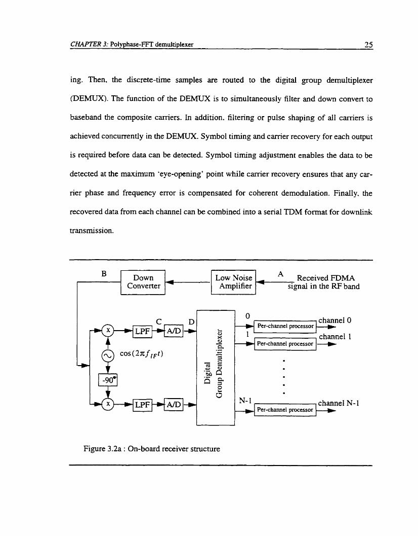
ing. Then, the discrete-tirne samples are routed to the digital group demultipiexer
(DEMUX). The function of the DEMUX is to simultaneously filter and down conven to
baseband the composite c k e r s . In addition. filtering or pulse shaping of al1 carriers is
achieved concurrently in the DEMUX. Symbol timing and carrier recovery for each output
is required before data c m be detected Symbol timing adjustment enables the data to be
detected at the maximum 'eye-opening' point while carrier recovery ensures that any car-
rier phase and frequency error is compensated for coherent demodulation. Finaily. the
recovered data from each channel can be combined into a serid TDM format for downlink
trmsmission.
Received FDMA signal in the RF band
1 ' 1 channel 1
Per-charinel processor
Figure 3.2a : On-board receiver structure

CHAPTER 3: Polyphase-FFï demultiplexer 26
w frequency B
Figure 3.2b: Frequency spectrum at points A,B .C,D,O, 1 ,N- 1

CHAPTER 3: Polyphase-FFT demultiplexer 27
3 3 Analysis of the Polyphase-FFT Digital Gmup Demultiplexer
3.3.1 The Input FDMA Signals
The anaiysis here follows that in [17] and is provided to clarify the functionality
and relationships of the group demultiplexer's building blocks. The input to the multi-car-
:v- l
rier demodulator y(t) is a baseband s ipa l consisting of N FDMA signais r,(t) and k = O
noise z( t ) . and is given by
For QPSK modulation, the kth FDMA signal takes the f o m
where Al, is the carrier amplitude. f is the frequency
( 3 2)
offset associated with the channel,
a,. is the data phase in the ith symbol interval, and h,( t ) is the transmitted pulse shape.
the impulse response of the transmit filter. The parameters yk and qI, represent random
timing and phase offsets. respectively. Figure 3.3 gives a mode1 for the baseband signai
y ( ? ) when the number of channels is 8. The eight channels are arranged such that
f i = (k + i) ,, where f, is the Frequency spacing between channels. Normally. one

CHAPTER 3: Polyphase-FFT demdtiplexer 28
would represent the baseband sipals as being symmetrically distributed about the zero
frequency mark, but the representation of Fig. 3.3 proves convenient as the total band-
width occupied by the sipals is. f, = N f, which is ako the sarnpling rate.
It is assumed that al1 the channels use the same transmit filter h , ( t ) , which in gen-
eral will have a root-Nyquist characteristic. Furthemore. it is assumed that the filtering
requirements are split between the transmitter and receiver. If the transmit filter takes on a
root-raised cosine characteristic with a rolloff factor P (Appendix C), then the signal will
occupy a bandwidth of ( 1 + P) f b , where f = 1 / T b is the symbol rate. The channel sep-
aration f, must then be ,pater than or equal to ( 1 + p) f [ 1 71, [ 1 81.

CHAPTER 3: Polyphase-FFT demultiplexer 29
3.3.2 The Polyphase-FFT Network
For the derivation of the multi-carrier demultiplexer structure based on the
polyphase-FFT network, we begin with the mode1 of Fig. 3.4 for the demultiplexing of a
single channel.
Figure 3.4: Mode1 for demultiplexing of a single channel
The process of isolating the signal in the kth channel involves shifting the signal to
baseband and filtering with a low-pass filter. Since the original signal was sampled at N
times the rate of a single channel, we can also decimate the output of the low-pass filter by
a factor of N. The sarnpled impulse response of the low-pass filter is denoted by h(nT, ) ,
and it is assumed that the sarne filter charactenstic is used in the demultiplexing of al1 the
channels, O I k I N - 1 . It is also assumed that h(n T,) is a finite impulse response filter

with NL taps. The equation for the cornbined frequency shifting and filtering operations is
then
NL
x,(mT,) = h ( n T , ) ~ ' [ m T , - n T , ] n = I
where
Therefore,
- j2xkrn e = 1 when k and m are integers and fa = ( k f 112) f,
If we now express n as
and sum over both v and p , Equation 3.3 can be written as

For each value of p . and across al1 values of v . each set of filter coefficients
h [ ( v N - p ) T,] c m be associated with a separate filter
In a similar fashion. the input signal can be written as N separate. decimated simals
If we combine Eq. 3.5 and Eq. 3.6, and let
then we obtain the final equation for the output
where "*" denotes digital convolution "L" denotes the number of taps per filter.

C H A P E R 3: Polyphase-FFT demultiplexer 32

CHAPTER 3: Polyphase-FFT demultiplexer 33
Working from right to left then, the set of operations defined by Eq. 3.8 is: a digital
filtering operation Pp(mT,)*Yp (m Tc) . multiplication by a set of phase offsets [ w ~ ~ - ~ ] .
iv- l
followed by a discrete Fourier transforrn [z W'kp]. and finally a set of diernating p = o
sign changes on the output [(-l . The filtering operation is performed at the lower
sampling rate f , = 1 / T c rather than the higher input sampling rate f = N f Figure 3.5
gives a block diagram of the o v e r d structure defined by Eq. 3.8. The Fourier transform is
performed on the signal z , (nT, ) which is the output of the polyphase filter multiplied by
the phase offset.
The filters &,(v Tc) are called polyphase filters. as the decimation process of Eq.
3.5 gives a set of filters with the same amplitude response but different phase responses.
Assurning that the original filter h( N Tc) has a linear phase response. the filter Pp ( V T c )
will have a linear phase response whose slope is a constant times p / N .
The fact that the polyphase filters have finite impulse response means that there
cannot be perfect separation between the channels and some interchannel interference or
crosstalk will occur. The design problem for the multicarrier demultiplexer is thus a
trade-off between rninirnizing the nurnber of taps L in the filters and reducing the degracia-
tion caused by the crosstalk to an acceptable level.

CHARER 3: Pol yphase-FFT demultiplexer 34
33.3 Interpolation in the Channel Processor for Rate Conversion
Following the multi-carrier demultiplexer is the channel processor where symbol
timing and cimier phase synchronization are performed. An imponant part of the channel
processor is the rate conversion stage where the input samples at rate f, = 1 / T c are con-
verted to a set of sarnples at the symbol rate f b = 1 /Tb. This rate conversion can be writ-
ten as a simple digital filtering operation [19].
where g(t) is the impulse response of the interpolaring filter.
The relationship betwqn the timing of the input samples xk(mT,) and the output
samples rk(ZTb) is illustrated on the time line of Fig. 3.6. Here it is seen that there are
several input samples for every output sample. but the timing of the two sets does not coin-
cide. Several new indices need to be defined. The first involves converting the signal index
m io a filter index i, where
< = int - - m 1 where int r z 1 is the largest integer not exceeding z.
Next. since the objective is to interpolate between the input samples to produce an
output sample at time ITb, we define the basepoint index P I as the index of the input

frac tional input sample tirnes
Pl T c / (Pl+ U T ,
LTb
basepoint index u+ 1 )Tb
output sampie times
Figure 3.6: Timing relationship between input and output samples in the rate conversion filter
sampie just preceding the Zth input sarnple.
The normalized time difference between the input sampie at time PlTc and the output
sarnple at lTb is referred to as the fractionai interval
Then using the indices of Eq. 3.10, Eq. 3.1 1 and Eq. 3.12, the rate conversion filtering cm
be rewntten as

CHAPTER 3: Polyphase-FFî demultiplexer 36
If g(t) is a finite impulse response filter then I I and 1, are fixed integers and "
1 = 1, - I I + 1 is the number of filter taps.
The value of P I and pl must be known to obtain the proper filter coefficients
g [ ( c + p,) T b ] . These rwo parametea are estimated by the timing recovery algorithm. In
general. a finite number of quantization steps has to be used for p, so that the filter coeffi-
cients cm be stored in rnemory. in the initial stages of analysis. it is usually assumed that
p, and p l are precisely known and then an attempt to determine the number of taps, L for
the polyphase filter and 1 for the rate conversion filters. to rninirnize the probability of
error is made. This is a reasonable assumption given that symbol synchronous transmis-
sion is being considered for many on-board processing systems. If symbol synchronous
transmission is used. then timing recovery is simplified and the rate conversion filter
works its way through a set pattern of filter coefficients. This would dso imply that the
timing offset y, in the nansmitted signal response for channel k is zero (perfect symbol
synchronization) or a random quantity of small magnitude.
In the rate conversion process. there is the choice of performing some of the
receiver filtering or it can be used simply as a delay to interpolate between the input sam-

CHAPTER 3: Poiyphase-FFT demultiplexer 37
ples xk(mTc) . In the latter case. the ideal choice for the impulse response g(t) is a sinc
function. However. the receivzr filter can be split between the polyphase filten Pp ( r Tc)
and the rate conversion filter. Lf the overail receiver filter characteristic is to be a root
Nyquist response, then the polyphase filters and the rate conversion filter will each
approximate a fourth-root Nyquist characteristic.
33.4 The Final Output
In order to analyze the system performance, the expression for the output of the
multisarrier demultiplexer has to be arrived at. It should clearly show that for the kth
channel the desired symbol is the ith symbol interval plus any unwanted interference
terms. To arrive at such an expression. the FDMA input of Eq. 3.1 and Eq. 3.2 are com-
bined with the demultiplexing Eq. 3.3 or Eq. 3.8 and the rate conversion process of Eq.
3.13. In terms of analysis it is easier to work with Eq. 3.3. To begin. the sarnpled input sig-
nal is given as
substituting Eq. 3.14 into Eq. 3.3. the demultiplexer output for the kth channel is

CHAPTER 3: Polyphase-FFî demdtiplexer 38
Next. proceeding through the rate conversion stage, the equation for the final output can be
given by
L itl
where

CH-R 3: Polyphase-FFT demultipIexer 39
and
1% The first term inside the square brackets on the right of Eq. 3.16. e u ( 0 ) . is the
desired symbol for the kth channel and the lth symbol interval. The second term in the
brackets represents intersymbol interference, while the final surnmation is the interchanel
interference or crosstaik from the N- l other channels.
3.4 Conclusion
nirough the anaiysis of the polyphase-FFT group demultiplexer, it is shown that
the demultiplexing of the FDMA signais can be achieved by means of a combination of a
polyphase network, phase shifters and an FFT processor.
Further. the sarnpling rate at the output of the demultiplexer is not suitable for the
subsequent demodulation process, where an integer number of samples per data symbol is
required. A sampling rate conversion filter is necessary for interfacing between the demul-
tiplexed channels and the demodulator.

CHAPTER 4: Acte1 FPGA Technology. CAD tools. Design and Test Enviromnent
CHAPTER 4
Actel FPGA Technology, CAD tools, Design and Test Environment
4.1 Introduction
The introduction of advanced CAD tools has greatly simplified the design and
implementation process, vastly reduced design cycle time and improved the quality of
products. Starting from a given design specification. CAD tools allow designers to capture
its schematic and perform extensive venfication and simulation at different levels.
This chapter discusses the Actel FPGA technology and tools, describes the CAD
tools, dong with the design and test environment which were used for the impIementation
of the group demultiplexer.

CHAPTER 4: Acte1 FPGA Technology, CAD tools, Design and Test Environment 41
4.2 Actel Antifuse FPGA Technology
Actel Corporation is a leading supplier of high performance field programmable
gate arrays (FPGAs) and provides antifuse based architecture in the FPGA market [20] .
Currently Actel is the only vendor manufacniring space qualified FPGA's. The environ-
ment in which the satellite operates necessitates the use of space qualified devices. Hence.
for the implementation of the group demultiplexer for sateiIite applications. the Actel radi-
ation-hardened FPGA is an appropriate choice.
4.2.1 Actel Device Architecture
The underlaying architecture of an Actel FPGA is very similar to that of a conven-
tional gate array. The core of the device consists of simple logic modules which are used
to impiement the required logic gates and storage elements. These logic modules are inter-
connected with an abundance of segmented routing tracks. The segmented lengths are pre-
defined and can be connected with low-impedance switching elements to connecr the logic
modules. Surrounding the logic core is the interface to the UO pads of the devices. This
interface consists of U 0 modules that translate and interconnect the logic signals from the
core of the device to the FPGA output pads. A block diagram of a genenc Acte1 FPGA is
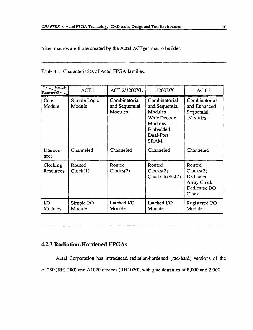
given in Fig. 4.1 [2 11. The major elements of the Actel FPGA architecture are thus, the I/0
modules, interconnect resources, clocking resources, and logic modules. Each Actel
FPGA family has a slightiy different rnix of these resources, optimized for different cost.

CHAPTER 3: Acte1 FPGA Technology, CAD tools, Design and Test Environmerit 42
I/0 Modules High-Drive Clock Buffer
I Logic Modules
VO
V O L
UO
V O L
Channel-Oriented Seagmented Routing Tracks
Figure 4.1 : Basic Actel FPGA architecture
/ l
/ 1 .- / 1 1 VO 1 \
Y 0 I 7
Y0 1
L L L L
I CLK
d L \ l 1
- I w v
L L L L L L L L L L V O
1
L
VO
L
L/0 Il0 VO VO Il0

CHAPTER 4: Acte1 FPGA Technology, CAD tools. Design and Test Environment 33
performance, and density requirements.
The Acte1 FPGA architecture is based on the progarnmable low impedance circuit
element (PUCE) antifuse technology. The PLICE antifuse is built using an oxide-nitride-
oxide (ONO) dielectric between N+ diffusion and polysilicon. The antifuse is functionally
opposite to a conventional fuse. An antifuse is a two terminal device with an unpro-
gramrned state presenting a very high resistance between its temiinals. When a high
voltage (16 volts) is applied across its temiinals, the antifuse will blow and create a iow-
resistance link, which is permanent [22].
A major advantage of the antifuse is its small size. This advantage is somewhat
diminished by the size of the transistors. which must be large enough to be able to handle
large currents, and the inclusion of isolation transistors that are needed to protect low volt-
age transistors from high progamming voltages. A second major advantage of an antifuse
is its relatively low series resistance. Aiso the parasitic capacitance of an unprogrmed
amorphous antifuse is si,pificantly lower than that of die SRAM, EPROM and EEPROM
prograrnming technologies [22].
The Actel logic block is based on the ability of a multiplexer to implement differ-
ent logic functions by connecting each of its inputs to a constant or to a signal [22] . For
example, consider a two-[O-one multiplexer with inputs. s (select signal), a and b and our-
put f = sa + Sb by setting signal b to logic 0. the multiplexer c m implement the AND
function f = su. Setting signal a to logic 1 provides the OR function f = s + 6. By con-

CHAPTER 3: Acte1 FPGA Technology. CAD tools, Design and Test Environment 4 4
necting together a number of rnultiplexers and basic logic gates. a logic block can be con-
stnicted which can implement a large number of functions in this manner. ln the ACT4
device. the sequential logic is not explicitly present and so must be fomed using program-
mable routing and the purely combinational logic blocks. In ACT-21200XL. ACT-3 and
32ûûDX devices there are two alternating types of Iogic blocks: the C-module which is
purely combinatorid, and the S-module which has similar combinational functionality to
the C-module but includes a D fiipfiop. The C-module is a combinatorid module opti-
mized to implement high fan-in macros such as 5-input AND. and 5-input OR. The S-
module is designed to implement high-speed sequential functions within a single module.
The S modules consist of a full C module driving a flip-flop, which allows an additional
level of logic to be implemented without additional propagation delay.
Multiplexer-based logic blocks have the advantage of providing a large degree of
functionality for a relatively smdl number of transistors. This is, however achieved at the
expense of a large number of inputs which when utilized place high demands on the rout-
ing resources. Such blocks are. therefore. more suired to FPGAs that use programmable
switches of small size such as antifuses.
The I/O modules provide the interface between the device pins and the logic array.
Low-skew. high fanout clock distribution networks are provided in each device. The Actel
architecture uses verticai and horizontal routing tracks to interconnect the various logic
and Z/O modules. These routing tracks are metd interconnects that may either be of con-

CHAPTER 4: Acte1 FPGA Technology, CAD tools. Design and Test Environment 45
tinuous lene@ or broken into pieces called segments. Varying segment leneas ailow the
interconnection of 90% of design tracks to occur with only two antifuse connections. Seg-
ments can be joined together at the ends. using antifuses to increase their 1engt.h up to full
length of the track. Al1 interconnects c m bc accomplished with a maximum of four anti-
fuses.
4.2.2 Actel FPGA Families and Macro Library
Acte1 offers ACT1 ACT2A300XL ACT3 and 3200DX families of devices which
represent different types of architectures. The user-definable I/07s are capable of driving at
both TTL and CMOS Ievels. Each U 0 pin is available as an input. output, three-state. or
bidirectional buffer. Table 4.1 shows the characteristics of Actel FPGA families [2 11.
When designing with Actel FPGAs, the appropriate library must be used. The ele-
ments available in each of the Acte1 Libraries are listed in the ACT Fmily Macro Library
Guide. The ACT family Macro Library consisü of six types of rnacros Hard. Soft. I/O.
TTL, M'AG. and ACTgen 'pararneterized macros.
Hard macros are logic elements constmcted of either one or two combinatorid
and/or sequential modules and cannot be modified. Soft macros are logic blocks con-
structed of multiple Hard macros, which can be modified, if necessary. U0 rnacros include
input, output and bidirectional buffee, latches and registers. TTL rnacros offer a variety of
logic functions which include adders, shiften, counten and registers. ACTgen parame-
CHAPTER 4: Acte1 FPGA Technology, CAD tooIs. Design and Test Environment 36
trized macros are those created by the Acte1 ACTgen macro builder.
Table 4.1: Characteristics of Actel FPGA families.
Core Module
Lntercon- nec t
Cloc king Resources
VO Modules
ACT 1
Simple Lugic ModuIe
Channeled
Routed Clock( 1 )
Simple I/O Module
ACT 2/1200XL
Combinatorial and Sequential Modules
Combinatorid and Sequentid Modules Wide Decode Modules Embedded Dual-Port SRAM
Channeled Channeled
Routed Clocks(2)
Routed Clocks(2) Quad Clocks(2)
Latched Il0 Module
Latched VO Module
ACT 3
Combinatorial and Enhanced Sequential Modules
Channeled
Routed Clocks(2) Dedicated Array CIock Dedicated I/O Clock
Registered UO Module
4.2.3 Radiation-Hardened FPGAs
Actel Corporation has introduced radiation-hardened (rad-hard) versions of the
A 1280 (RH 1280) and A 1020 devices (RH 1 MO), with gare densities of 8,000 and 2,000

CIiAPTER 4: Acte1 FPGA Technology. CAD tools. Design and Test Environment 47
array pates. respectively [23]. The feanires of these device include total radiation dose
capability, low single event upset susceptibility, high dose rate survivability and latch-up
irnmunity, as indicated in Table 4.2.
The target specifications for the Actel radiation-hardened devices 1231 as com-
pared to the typical values for radiation hardened technolog [24], [25] and Harris radia-
tion hardened CMOS/SOS family [26] are @en in Table 4.2. The &en values represenr
threshold values. beyond which the devices are likely to fail.
A description of the parameters included in Table 4.2 is provided here. Total dose
is the measure of nuclear radiation energy absorbed. Low rates of ionizing radiation have
negligible effect on circuit operation. The amount of total dose received is measured in
rad. Single event is a single, highly ionizing particle travelling through a memory circuit.
Single event upset (SEL?) is a transient change in circuit biases which can cause transient
errors in the circuit. Latchup refers to any stable or quasi-stable mode of device operation
in which the postradiation relationship between device's electrical input and output differ
significantly from the preradiation relationship for these parameters. Neutron Auence is a
measure of the neutron irradiation which can damage circuits by knocking silicon atoms
7
out of their place in the lanice structure. It is measured in neutrons/crn-
The RH1280 and RH1020 devices are Iatch-up immune, indicating that no cata-
strophic failures will uccur. Single event upsets can occur in these devices as with other
commercial serniconductor chips, but the rate of upset is low. as shown in the target speci-

CHAPlER 4: Acte1 FPGA Techology, CAD twls. Design and Test Environment 38
Table 4.2: Radiation-hardened target specifications
Total Dose , mdad* I Feanire
ACTEL specifications
Single Event Upset (SEU)
< IO-' errorshitday
Latchup
Survivability 1 > 1 O " rad(8 i)/sec
- - - --
h u n e
Dose Rate Upset
Neutron Flu- ence 1 > 1014 /cm2
> 1 O' rad(Si)/sec
Immune
Typical specifications
1 Immune
Hams specifications
* rad is a measure of absorbed energy, here in silicon.
fications. The total dose, dose rate upset and neutron fluence are comparable with other
radiation-hardened devices. The RH 1280 and RH 1020 are supported by Actel's Designer
and Designer Advantage Systems. These devices are targeted for use in rnilitary and space
applications subject to radiation effects.
4.2.4 RH1280 and A1280XL device features
The implementation of the group dernultiplexer was done on the RH1280 as well
as the A 1280XL devices. The basic features of these two devices are listed in Table 4.3

CHAPZER 4: Acte1 FPGA TechnoIom. CAD tools. Desi.en and Test Environment 49
Table 4.3: Features of Actel RH1280 and A 1280XL devices
L
Total no. of pins
Total logic modules C-modules S-modules
User pins
Total logic gates
1 CMOS ~rocess 1 0.6 micron 1 0.8 micron 1
160
1 Speed Grade 1 -2(3) 1 S T D - 3 ~ ~ 4 1
172
125
8000
1 Application(5) / Commercial 1 Commercial l
140
8000
( 1 ) Plastic Quad Flat Pack (PQFP) (2) Cerarnic Quad Flat Pack (CQFP) (3) Speed Options available for the A 1 BOXL are
STD = standard speed -2 = approximately 25% faster than STD (-1 corresponds to 15%)
(4) Speed Options available for the RH1280 are STD.O.KR = standard speed with O rad radiation dose level
STD.300.KR = standard speed with 3 x 10' rad radiation dose level (5) Temperature and voltage ranges
Both device types can be simulated under the best typical and worst case operat-
ing conditions. The specifications for the three conditions for commercial applications are
listed in Table 4.4

C K 4 R Z R 4: Acte1 FPGA Technology. CAD toois. Design and Test Environment 50
Table 4.1: Specifications for the operating conditions !cornmercial applications)
Voltage Case
Worst
4.2.5 Actel FPGA C m Tools
Temperature
L
B est
The Actel FPGA C m tools are referred to as the Designer Senes Development
System. The Designer Series software is used in the design. optirnization and prograrn-
ming of A& FPGAs. The Designer Series software inclrides the following software pro-
gams:
- ACTgen macro builder: enables creation of macros. This tool supports the creation of a
ua.riety of macros such as adders, subtracten, accumulators. comparators, counters. decod-
ers. multiplexers, shift registers, storage registes, latches and VO macros. It allows the bit
width and the set of control signals present on a rnacro to be defined. These rnacros opti-
rnize the Actel architecture with respect to performance and module count according to
the required specifications,
- ACTmap VHDL synthesis: provides a simple user interface for synthesis. logic optimi-
zation, retargeting among FPGA families and importing of existing PAL designs,
70 O C 4.75 V
O OC 5.25 V

CHAPTER 3: Acte1 FPGA Technolo-W. CAD tools. Design and Test Environment 5 1
- DESIGNER: provides an environment for checking and optimizing the netlist (Compiie),
assigning pin information (PinEdit), editing and placing macros (ChipEdit), assigning tim-
ing information (DTEdit), mapping the design into silicon (Layout). debugging
timing problems (DTAnaiyze). creating a file that is used to program the device (Fuse).
and extracting delays for back annotation(Extract),
- APSW/APS?: enables the programming of Actei FPGA devices.
4.2.6 Actel FPGA Design Cycle
The design process for using Actel FPGAs requires the following steps:
1. Entering the design in the fonn of schematic. netiist. logic expressions, or hardware
description langages.
2. Simuiating the design for functional verification,
3. Mapping the design into the FPGA architecmre.
4. Placing and routing the FPGA design.
5. Extracting delay parameters of the routed design,
6. Resimulating for timing verification,
7. Generating the FPGA device configuration format
8. Configuring or pro,oramming the device.
9. Testing the product functionai behavior.

CHAPTER 4: Acte1 FPGA Technolow. CAD tools. Design and Test Environment 52
Steps 1. 2 and 6 were done using Mentor Graphics CAD tools. The group demulti-
plexer was enrered in the fonn of a schematic using Design Architect from the Mentor
Graphics CAD tools. Macros from Actel A m 2 Iibraries and those generated using the
Actgen tool were ased in the schematic. Steps 1 and 6 were done using the Quicksim sim-
ulator tool from Mentor Graphics. The design was simulated for operation under the
worst, typical and best operating conditions. Steps 3 and 4 involve several processes: logic
minimization. technology mapping, placement and routing. which were done using the
Actel Designer Series Software System Logic minimization is done by the "combiner"
which is integrated into the Compile hinction of the Designer series software system. It
irnproves the design in terms of density, speed and routability by perforrning the functions
of combinatorid module reduction, sequential remapping, unused Iogic removai, constant
output reduction and fan-in reduction. Technology rnappinp binds the technology-inde-
pendent description of the circuit to the basic entities of the Actel technology. Placement
allocates these entities to the specific physical block on the device. Routing establishes the
connections between different blocks. Placement and routing was done using the Layout
tool. Step 5 was camied out using the DTAnalyze feature of the Actel Designer series soft-
ware. m i s includes a static timer tool which was used to determine the delays through the
circuit. Steps 7 and 8 were performed using the Fuse and APSW/APSZ tools. Figure 4.2
depicts the interface between the Mentor Graphics tools and the Actel tools.

CHAPTER 4: Acte1 FPGA Technologv. CAD tools. Desipn and Test Environment 53
1 1 Acte1 Tools 1
Figure 4.2: Standard flow for FPGA design based on the Actel and Mentor Graphics tools

Ch%PTER 4: Acte1 FPGA Technology, CCA tools, Design and Test Environment 54
4 3 Mentor Graphics Design Environment
Below is a brief description of the Mentor Graphics CAD tools which were used
for the present work. The Faicon Frarnework is a powerful common environment in which
al1 Mentor Graphics applications mn. These applications use the Faicon Framework to
provide a common user interface, text editor and decision support system. The Falcon
Frarnework consists of the Design Manager and other applications. The Design Manager
allows the user to view and navigate design data. move, copy and manage data and invoke
applications.
Design Architect is a tool box containhg a collection of tools (graphic and test edi-
tors) that are used to create and rnodify the data that is modelling a design. The three pri-
mary tools in the Design Architect are the Symbol Editor, the Schematic Editor, and the
VHDL Editor.
Quicksim II within the Mentor Graphics tool set simulates a digital schematic
design from Design Architect. Simulation is the rnodelling and behavioral analysis of an
electronic design without actud physicai hardware implementation.
4.4 Conclusion
This chapter provided an overview of the Actel FPGA technology with emphasis
on architecture. capabilities and design cycle. The CAD tools from Mentor Graphics and
Actel were also discussed. The Actel tools are interfaced with the Mentor tools to faciIi-

CHAPTER 4: Actel FPGA Technology, CAD tools. Design and Test Environment 55
tate design and implementation of the circuit-
Actel supplies the only radiation-hardened FPGA's available today. The RH 1280
and RH 1020 are radiation-hardened versions of the A 1280A and A 1020A devices with
mate counts of 8000 and 1ûûû gares respectively. In addition to being radiation-hardened CL
these devices incorporate ai1 the other features of the A 1280A and A 1020A devices. The
Acte1 radiation-hardened device specifications are comparable to those of other radiation
hardened devices. These devices are suited for applications which are subject to the effects
of radiation.

CHAPTER 5: Polyphase-FFT Group Demultiplexer System -4rchitecnue
CHAPTER 5
Polyphase-FFT Group Demultiplexer System Architecture
5.1 Introduction
In this chapter the building blocks for the polyphase-R goup demlltiplexer are
identified and the architecture of the polyphase-FFT s o u p demultiplexer is reviewed. This
chapter addresses the interfacing between the building blocks of the polyphase-FFT group
demultiplexer and discusses the input. output and clock requirements for the building
blocks and the systern. The delay introduced by the input and output pads for each device
used in the implementation is also discussed.

CHAPTER 5: Polyphase-FFï Gmup Dernultiplexer System Architecture 57
5.2 Builduig Blocks and Architecture of the Polyphase-FFT Group Demultiplexer
The basic building blocks in the smcnire of the polyhase-FFT poup demulti-
plexer are the commutator. a bank of polyphase subfilters. a set of phase shifiers. FFT pro-
cessor and a set of sign inverters. Figure 5.1 depicts rhe building blocks for the polyphase-
FFT group demultiplexer.
To recover the signal in each of the N channels, the received FDMA signal in the
baseband is passed to a commutator which separates the input sarnpled data into N differ-
ent substrearns. The sarnpled data is processed in a parallel fashion by the polyphase sub-
filters. and the sampling rate is reduced by N tirnes due to decimation by the comrnutator.
Each data Stream goes into a digital subfilter. This set of subfilters is referred to as a
polyphase filter bank.
The outputs from the polyphase filters are then multiplied by the phase shifts
before being processed by the FFT processor. The signs of the FFT outputs are invened
for every other sample to yield the demultiplexed QPSK sigals in the baseband. To facil-
itate processing by the demodulator, a sampling rate conversion filter is needed at the out-
put of the demultiplexer for each channel.

CEMPTER 5: Polyphase-FFï Group DemuItiplexer System Architecture 58

C m 5: Polyphase-FFT Group Demuitiplexer System Architecture 59
53 System Specifications and Parameters
The basic system parameters of the implemented group demultiplexer are summa-
rized in Table 5.1 and the parameters for the polyphase subfilters, FFT processor and a
representative rate conversion filter are surnmarized in Table 5.2. These parameters are in
accordance with the research work done at CRC [18], [ I l . Two's complement &thmetic is
used in the implementation of the building blocks.
Table 5.1 : System parameters of the implemented group demultiplexer
Parame ter - - -
Modulation scbeme used for the input
Number of QPSK s i p d s
Channel separation
Total bandwidth of the modulated signal
Data symbol rate (Tl rate) Data symbol rate with 314 convolutional coding
Sarnpling frequency for real and quadrature - --
Input / Output resolution
Filtering -- - --
Roll off factor for the filter
Description
QPSK
1.544 MHz
12.352 MHz
0.772 Msampies per sec
1 .O29 Msamples per sec
12.352 MHz
8 bits112 bits
full raised cosine Nyquist
The results presented in [18] indicate that acceptable performance in terms of the
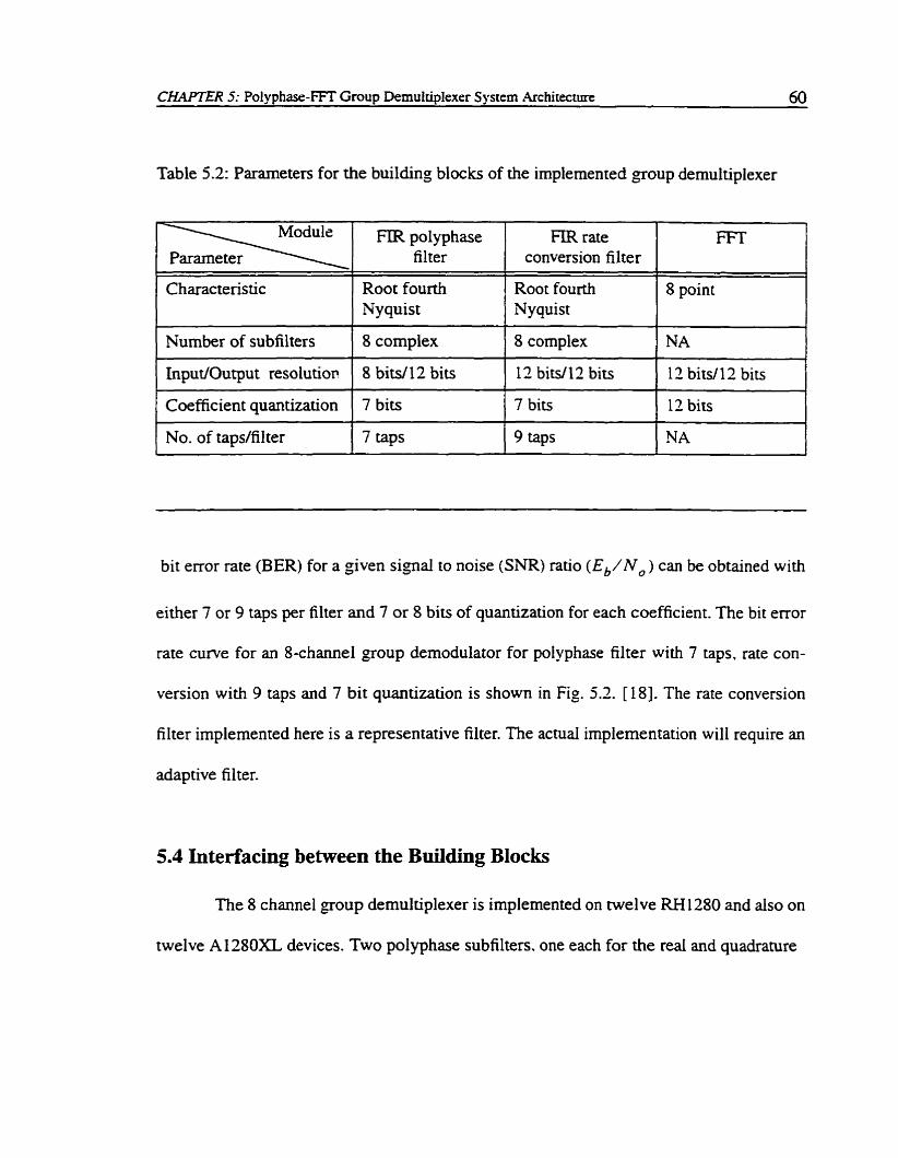
ChXPïER 5: Polyphase-FFT Group Demuitiplexer S ystem Architecture 60
Table 5.2: Parameters for the building blocks of the implemenred group demultiplexer
Nyquist - -
Number of subfilters
InputfOutput resolutio~
FR rate conversion filter
Root fourth Nyquist
8 complex
8 bits/ 12 bits -
Coefficient quantization
No. of taps/filter
7 bits
7 taps
8 complex
12 bitsll:! bits
bit error rate (BER) for a given signal to noise (SNR) ratio ( E b / N , ) can be obtained with
either 7 or 9 taps per filter and 7 or 8 bits of quantkation for each coefficient. The bit error
rate curve for an 8-channel group dernodulator for polyphase filter with 7 taps. rate con-
version with 9 taps and 7 bit quantization is shown in Fig. 5.2. [18]. The rate conversion
filter irnplemented here is a representative filter. The acniai implementation will require an
adaptive filter.
NA
12 bits11 2 bits
7 bits
9 taps
5.4 Interfacing between the Building Blocks
The 8 channel group demultiplexer is implemented on twelve RH1280 and also on
twelve A1 280XL devices. Two polyphase subfilters. one each for the real and quadrature
12 bits
NA


ChWT&R 5: PoIyphase-FFï Group Demultipiexer System Architecture 62
inputs with the corresponding phase shifier is implemented on a single device. The imple-
mentation of the eight polyphase subfilters for the real inputs. eight subfilters for quadra-
ture inputs with the corresponding phase shifters thus requires a total of eight devices. The
8-point d i x - 2 . Decimation-in-Time (DIT) FFT is implemented on four devices. The sign
inversion of every aiternate output of the FFT is done in the devices on which the third
stage of the FFT is implemented. The two rate conversion filters for each channel for the
real and quadrature inputs are implemented on one device. Hence. eight cornplex rate con-
version filters for al1 eight channels of the group demultiplexer require eight devices for
realization.
Proper interfacing between the devices used for the implementation of the group
demultiplexer ensures desired functionality. Figure 5.3 depicts the interfacing between the
twelve devices used in the implementation of the polyphase-FFT g o u p demultiplexer.
Devices representing the polyphase subfilters and phase shifters are denoted by p l to p8.
the FFT processor by fla, f lb, fZ a n d p .
In th is implementation, the address bus a l (3 bits) is used to route the input data
samples from the AID converter to the appropriate filter. This enables the implementation
to be extended easily to a Iarger number of channels, simply by using more devices for the
extra channeis and increasing the number of bits for the address line. The Iimited number
of user inputloutput pins available for each device dictates the manner in which the data is
routed between the various building blocks. Also, the architecture of the building

CHAPTER 5: Polyphase-FFT Group Demdtiplexer System Architecture 63
pn polyphase subfiiter (cornplex) & phase shifter for channei n f FFï device
œ u - 16-bit data bus @-bit r e d & &bit complex) - 24-bit data bus ( 12-bit real & 12-bit complex) - 3-bit address bus
(di data buses arc complex)
Figure 5.3: Interfacing between the 12 devices used in the implementation of the polyphase-FFT demultiplexer

CHAPTER 5: PoIy phase-FFT Group Demdtiplexer S y stem Architecture 64
blocks and the interfacing beween them is chosen to keep the gate count and the U 0 count
as low as possible. in order to keep the power dissipation of the device to a minimum. The
interfacing between the devices is sumrnaized here with reference to Fig. 5.3.
Two 8-bit data bus (il) each for the rea! and quadrature data sarnples fiom the A/D
converter are routed to each of the devices @1 to p8) of the polyphase subfilters. In each
device a decoder circuit decodes the 3-bit address line (al) and routes the input data Sam-
ple to the subfilters. The 12-bit complex data sample output from the subfilten for each
channel is processed by the corresponding phase shifter. The Il-bit complex output data
samples from the phase shifter are then processed by an FFT. The 12-bit complex data
samples from channels 1. 2,3 and 4 are routed on a 12-bit complex bus (i2). Similarly, the
12-bit outputs from channel 5 , 6 , 7 and 8 are routed on bus i3. The throughput capabilities
achieved for the butterfly in the first stage enabled it to be reused. As a requirement for
this. the data is routed on two buses to the FFT. Limited number of inpuidoutput pins on
each device prevented a separate 12-bit complex bus to be used for each channel. The
FFT's output data sarnples are routed on four 12-bit complex buses (i4, i.5, i6 and i7). with
the output for two channels available on one bus.
5.5 Clocking Scheme
Circuits operating at lower rates have iower power dissipation, and hence it is
desirable that the logic module switching rate be as low as possible. For the polyphase-

CHUTER 5: Polyphase-FFT Group Demuitip lexer S y stem khitecture 65
FFi' group demultiplexer the building blocks operate at 1/N (N is the number of channels)
Urnes the input sampling rate. This enables the polyphase filters. FFT and the rate conver-
sion filters to operate at a lower frequency resulting in a reduction in the power dissipation
of the devices on which they are implemented.
Clock skew can cause setup and hold time violation problems. hence the system
clock needs to be routed to al1 the twenty devices, through a low skew network. Two dedi-
cated subnano second skew networks [20] with high fanout, available in the RH1280 and
A1280XL devices are used ta route the system dock and the lower frequency clock within
each device. The low frequency clock may either be made available from an external cir-
cuitry or may be generated within each device. Since the number of logic b!ocks required
to generate the clock within the device is very low. approximately 0.38 of the total blocks
per device, and generating a clock inside each device reduces interfacing, routing and
skew problerns, this approach is used here.
To ensure minimum power dissipation. each of the polyphase subfilters is operated
at the low frequency of 1/8 the sarnpling frequency. The address line in synchronism with
the system clock is decoded to generate the clock for each channel. The timing relation-
ship between the clocks for the 8 channels is depicted in Fig. 5.4.
The low frequency clocks for the rate conversion filter are generated by decoding
the address lines, in a manner similar to the one used for the polyphase subfilters.
The nature of the implementation of the FFI' requires that the first stage of the FFï
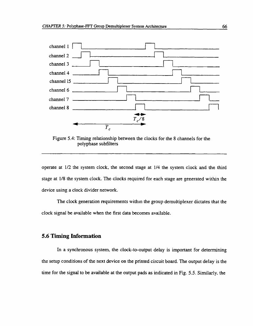
CHAPTER 5: Polyphase-FFT Group DemultipIexer System Architecture 66
Figure 5.4: Timing relationship between the cIocks for the 8 channels for the polyphase subfilten
operate at 1/2 the system clock, the second stage at 1/4 the system clock and the third
stage at 1/8 the system clock. The docks required for each stage are generated within the
device using a dock divider network.
The clock generation requirements wirhin the group demultiplexer dictates that the
clock signal be available when the first data becomes available.
5.6 Timing Information
In a synchronous system, the dock-to-output delay is important for determining
the setup conditions of the next device on the printed circuit board. The output delay is the
time for the signal to be available at the output pads as indicated in Fig. 5.5. Similarly, the

CH- 5: Polyphase-FFT Group Demdtiplexer System Architecture 67
input delay is the time for the signal to amve on-chip from the input pads. This informa-
tion is needed to provide proper delays for the interconnects between the devices on the
printed circuit board. Delay through the interconnect between two devices should be less
than the difference of the system clock and the sum of the input delay of the second device
and the output delay of the first device.
register Inbuf -
Input delay (from PAD to D)
Output delay (from PADin to PADout)
Figure 5.5: Input and output delays
The post layout timing delays for the inputs and outputs for the devices used in the
implementation of the group demultiplexer are provided in Appendix A. From the data
presented, it is observed that for the wont and typical case operating conditions, the
A1280XL devices have 20-40% lower delays than the RH1280. However, for the best

CHAITER 5: Polyphase-FFT Group Demultiplexer System Architecture 68
case operating condition the delays of the two devices are comparable. A similar trend in
the performance is observed for the logic modules and is presented in a later chapter. The
reason for this difference can be attributed to two factors. First, the A1280XL devices are
processed in 0.6 p technology while the RH 1380 are processed in 0.8 p technology mak-
ing the -4 1200XL faster. Second. the A1280XL devices used for the implementation are
speed grade -2 which is about 25% faster than the standard speed that is used for the
RH 1 280 devices.
Anothcr point of interest is the fact that tristate output buffers used for the
polyphase subfilters exhibit longer delay (108) as compared to the output buffers without
tristate logic. This observation is of consequence for high speed circuits where the use of
tristate output buffen rnight slow down performance. For high speed circuits. manual
input/output pin placement may be used to reduce the delays through the inputfoutput
pads.
The input and output delays also provide information regarding the maximum
delays pemiissible between devices. From the computed data for worst case operating
conditions. the delay permissible between the devices is presented in Table 5.3. These val-
ues do not incorporate the delay through the clock buffer and the effect of the clock skew.
If the delay through the clock buffer, which is approximarely lOns for worst case operating
conditions and 3 ns for best case operating conditions, is taken into account the values in
Table 5.3 should be augmented by at least 3ns.

CHAPTER 5: Pofyphase-FFI' Group DemuItiplexer System Architecture 69
Table 5.3: Permissible interconnect delays between devices
Pennissible delay Permissible delay Between devices 1 RH1280 1 A1280XL
pl to p8 and fla & f lb
The polyphase subfilters and the rate conversion filters can be reset using the clear
signai, whose characteristics are such that it m u t be active low for 7511s or more.
l
42.4 ns 1 55 ns
I 1
fla & f lb and
5.7 Conclusion
This chapter described in detail the interfacing between the building blocks and the
devices used in the implementation of the polyphase-FFT demultiplexer. The timing infor-
mauon which is very critical to the functioning of the system was also provided.
For low power dissipation and increased reliability it is desirable to keep the U 0
pins to a minimum and to operate the logic modules at the lowest possible frequencies.
The dedicated low-skew networks available on the A 1 ZOXL and RH 1280 devices, used
to route the clocks, keep the clock skews within each device to subnano second values.
Proper setup and hold times between the devices need to be provided to enable the
data samples to be correctly transferred and latched. The input and output delays provide
the information necessary to ensure that.
52 ns 62.3 ns

CHAP77Z.R 6: Polyphase-FET Group Demultiplexer implementation
CHAPTER 6
Polyphase-FFT Group Demultiplexer Implementation
6.1 Introduction
There are a number of ways in which each building block of the polyphase-FFT'
oroup demultiplexer c m be implemented on an FPGA. The optimum design requires a 2
consideration of the routing and logic block architecture of the FPGA k i n g used.
The building blocks hardware design is based on the functional, fixed word mathe-
matical representation. This chapter presents the manipulation of the original equations
(Chapter 3) !eading to a final hardwae representation for each of the building blocks. A
detailed description of the implementation of the building blocks on the Acrel RH 1280

CHAPTER 6: Poiyphase-FFT Group Demultiplexer Irnplementation 71
and A1280XL devices is given. Results for the implementations describing their perfor-
mance in terms of speed and device utihzation are also provided.
6.2 Polyphase Filter Network
The analysis here is based on [2]. Each data substream at the output of the comrnu-
tator goes into a digital subfilter. These subfilters are denved from a prototype filter. Let
h [ n ] be the prototype filter with sampling frequency l/T,, then the digital subfilter
impulse response is defined as
hk[n] = h[nN + k] ( -1 )"
h k [ n ] has sampling interval Tc which is equal to NT,.
Let H o ( o ) be the frequency spectnim of h o [ n ] . then
- jwn Tc = C h * W , ) e
where w is the frequency in radians per second. Similarly, the frequency response of the

CHAPIER 6: Polypbase-FFT Group Demultiplexer implemenration 72
H k ( m ) = h k [ n ] e - jon Tc
The set of subfilters h k [ n ] is called a polyphase filter bank since each path
approximates a pure phase-shifter with the same frequency but different phase shifts. To
minirnize intersymbol interference. the system employs raised-cosine pulse shaping which
is shared equally between the vansrnitter and the receiver. Thus, each received signal has
been shaped by square-root raised cosine filter [Appendix Cl. The prototype filter h [ n ]
has frequency response of a founh-root raised-cosine with baud penod T. That is,
where h R C i I 4 ( f ) 1 is a founh-root raised cosine filter. The full raised-cosine response c = nT,
will be obtained by passing the output to another fourth-root raised cosine filter in the per-
charme1 processor. Figure 6.1 depicts the decomposition of the hRcl,&z] with N=4.

CHAPTrR 6: Polyphase-FFï Group DernuitipIexer implementatïon 73
Figure 6.1 : Decornposition of h R C l , 4 [ " 1 with N=4
(a) Before decomposition hRcv4 [ n j
h R , d 4 n + 0 1
CHM7ER 6: Polyphase-FFT Group Demultiplexer hplementation 74
The filtering of the complex signal by the subfilter is performed by passing the reai and
irnaginary parts of the signal into two identical subfilters since the coefficients of the sub-
filters are real.
6.2.1 Filter Coefficients for the Polyphase Network
The coefficients for the polyphase filter were derived usinp the Matlabz based soft-
ware cieveloped at CRC [18]. The design method for the filter is to build a prototype filter
of 8 192 taps startïng in the frequency dornain and using an inverse FFT to get the time
domain response. The impulse response of the filter is then mncated to the desired num-
ber of taps. This is done to get better accuracy on the coefficients. The polyphase proto-
type filter gives the 56 taps used in the implementation of the 8 polyphase subfilters. The
frequency response of the prototype is a fourth root raised cosine response to split the
receiver filtering between the polyphase network and the rate conversion filter. The pararn-
erers chosen for the polyphase filters are iisted in Table 6.1. A list of the coefficients for
the polyphase filters is provided in Appendix B.
6.2.2 Implementation of the Polyphase Subfilters
An 8 channel group demultiplexer with complex inputs is implemented. Each
* Mahx Laboratory software package for technicd computing from The Math Works Inc.

CHAPTER 6: Po!yphase-ïFï Group Dernultiplexer Implementation 75
Table 6.1 : Parameten for the polyphase tilters
Parameter Value
Normalized fiequency spacing (Fs) 1.5
Number of channels
Rolloff factor for the raised cosine filter
--
8
0.4
Window used
Beta factor for the Kaiser window
Kaiser
- 7
Number of taps per subfilter
Number of subfilters
Total number of taps
polyphase subfilter is implemented as an FIR filter with 7 taps, with 7 bits of quantization
for the coefficients [Ml. The inputs are complex but the coefficients are red, hence input
for each channel needs two subfilters to generate the complex output. Two's complement
fixed format arithrnetic has k e n used in the implementation of the polyphase subfilters.
The inputs to the polyphase subfiiter are 8 bits integers. represented in binary fixed format.
7
8
56 - - -
Number of bits per filter taps
The mors due to mincation in the polyphase filter ranges frorn (-2-" to O). The
errors due to format conversion are not considered here. Assuming the errors to be uni-
--
7
formly disuibuted randorn variables, the variance due to thesc errors is given by 2-24/ 12.

C H A f E R 6: Polyphase-FFT Group Demultiplexer Implementaaon 76
For the FIR filten with 7 taps the output is given by Eq. 6.5.
To implement the FR filter. the six previous output sarnples are stored in registers. The
previous samples and the current data sample multiplied by appropriate coefficients are
added to compute each output sample. The subfiltea are implemented by simple add and
shift operations where every shift operation is hardwired. The architecture and implemen-
tation methodology for the subfilter for channel 1 is presented here. The architecture and
implementation methodology for the other subfilters is identical to the one discussed.
The output for the subfilter for channel 1 corresponding to the direct form realiza-
tion of the subfilter is given by Eq. 6.6 and is graphically represented in Fig. 6.2.
This equation is modified to result in powers-of-two multiplications. Power of two
multiplications can be realized in dedicated hardware by simply shifting the data to the lefi
or right by an appropriate number of bits. The resulting hardware is a small fraction of the
hardware needed to implement a general purpose multiplier. Equation 6.7 shows the mod-
ified equation which results in powers-of-two multiplication.

CHAlTER 6: Polyphase-EFï Group Demuitiplexer Implemeotation 77

CHAPTER 6: PoIyphase-FFT Group Demultipiexer Implementation 78
From Eq. 6.7 it is evident that al1 the multiplications c m be performed by appro-
priate shifüng of input signals. Thus, the operation of multiplication and accumulation for
the RR filter c m be performed by shift and add operations. Equation 6.7 can be written as
y = x 1 t (-x2 shifted 3 left) + (-x2) + (x3 shifted 5 left) + (x3 shifted 4 left) + (-x3 shifted 1 left) + (x4 shifted 5 left) + (x4 shified 4 left) + (-x4 shifted 1 left) + (-x5 shifted 3 lefi) -
partial product
x 1 xl, 2. -4 x2*. --i- x y
C x6 , t delay(registers )
Panial products generated by shifting the inputs I
Addition of partiai products using Carry Save Adders
Final Adder
f Output
Figure 6.3: Block diagram for the impiementation of the polyphase subfilters

CHAPTER 6: PoIyphase-FFT Group Demultiplexer implementation 79
The input samples are shifted to generate the partial products. The partial products
are then added using carry Save adden (CSAs) to generate the final output. Figure 6.3
shows the block diagram representation for the implementation of the polyphase subfil-
ters.
The phase shifters which operate on the output of the polyphase subfilter. are
implemented as complex multiplications by fiactional numbers. The output of the
polyphase subfilters are converted to binary fractional format and truncated to 12 bits to
enable further processing by the phase shifter. Representing the output as a fixed-point
fraction ensures that the product of two numbers remains a fraction and prevents overflow
due to multiplication. Also, fixed word length can be maintained by uuncating the least
significant bits [27]. The binary fractional fixed format representation is depicred in Fig.
6.4.
e-g. (0.1 Iûûûûûûûûû), represents (0.75) the decimal point is assumed
( 1 -0 1000000) , represents (-0.75)
The first bit represents the sign bit. For a number x represented in this format the
rangeis (-1 5 x c 1 )
Figure 6.4: Binary fractional fixed format representation

C m R 6: Polyphase-FFT Group Demultiplexer lmplementation 80
6.2.3 Comparison of Dinerent Architectures for the Implementation of the Polyphase Subfilters
Two architectures for the polyphase subfiltea were implemented on the Actel
devices. The firs: implementation is discussed in Section 6 -22 . For the second implemen-
tauon, Eq. 6.6. for channel I subfilter was modified to
The input data samples to be multiplied by the same coefficients were added and
then add and shift multipliers were used to generate the partial producü. The partial prod-
ucts were then added using CSA adders and combined in a final addition stage.
Comparison of the architectures showed that the implementation discussed in 6.2.2
used a lesser number of CLB's as compared to the irnplementation of Section 6.2.3. How-
ever the implementation of Section 6.2.3 was marginaily fasier than the irnplementation of
section 6.6.2. Since both implementations were operationai for the required speed. it was
decided to use the implementation of Section 6.2.2 which resulted in the use of lower
number of logic modules. Usage of lower number of logic modules enabled the subfilters
and phase shifter for a channel to be implemented on a single device, thus reducing the
numben of devices required for the implementation of the group demultiplexer.

C H A P E R 6: Poiyphase-FFï Group Demuitiplexer hplementation 8 1
6.3 Phase Shifters
The phase shifting at the output of the subfiiten is implemented as a muiùplication
by ëJn"'" where n is the number ranging from O to N- 1 and N is the number of channels
in the group demultiplexer. The complex phase shifier operates on the output of the red
and imaginary subfilter for a particular channel. The list of phase shifter multiplien for
each of the channels is provided in Appendix B.
63.1 Implementation of the Phase Shifters
Twelve bit binas, fractionai fixed format is used in the implernentation of the
phase shifters as discussed in Section 6 - 2 2 The input to the phase shifter for each channel
is the cornplex output of the polyphase subfilter for that channel. To maintain fixed word
size the complex outputs from the phase shifters are tnincated to 12 bits. Each complex
multiplication requires four real multiplications. Truncation is used in the multiplier to
limit the word size to 12 bits. The variance of tnincation errors for each real multiplier is
,-24 - / 12 , and for the cornplex multiplier it is 2-"/3 [BI.
C H . 6: Polyphase-ïFï Group Demultiplexer hpiementation 82
6.4 Implementation Resuits for the Polyphase Subfilters and the Phase S hifters
The subfilters for the real and imaginary inputs with the corresponding phase
shifter are implemented on a single RH1280 device and also on the A1280XL device.
Each device has two FIR subfilten each with 7 taps and 7 bit coefficients for the taps and a
phase shifter for that particular channel. The 8 channel filter bank of the goup demulti-
plexer consists of 8 subfilters for the real inputs. 8 subfilters for the imaginary inputs and 8
phase shifters. A totai of eight devices have been used ro implement the polyphase filters
and the phase shifters.
The resuks for the post-layout implernentaion on the RH1380 and A1280XL
devices have been sutrmarized in Tables 6.2a and 6.2~. The po!yphase subfilters were
tested at a system operating frequency of 24 MHz (41 -6 ns clock period) and 3 .MHz
(332.8 ns clock period) for each subfilter. The functionality of the circuit was verified for
the worst, typical and best case operating conditions through simulations. The delays are
determined by the static timer tool from Actel. Static timing results show that the designs
are capable of operating at a system clock rate of 38 MHz for the RH1 280 device and 56
MHz for the A128OXL and the device operating internally at a clock rates of 4.75 MHz for
the RH1280 device and 7 MHz for the A1380XL
The device utilization (percentage of CLBs used) for both the RH1280 device and
the A1280XL device is identicd since they have the same number of CLBs. For ACT3
designs usually 100% of the CLB modules can be used without difficulty, but excessive

CHAPTER 6: Polyphase-FFT Group Demultiplexer Implementation 83
use of registers may make placement difficuit [29]. For the polyphase subfilters and phase
shifter implementation. designs with up to 99.19% device utilization were placed and
routed successfully, and simulated to ensure proper functionality.
The maximum register to register delay is an indication of the maximum operating
frequency for a design. In a data path architecture design. the maximum operating fre-
quency is the inverse of the longest register to register delay. The register to register delay
is defined here as the delay between two registers, from the clock edge at the first register
to the input of the second register, including al1 combinatorid gate deiays between the reg-
isrers and the required semp time of the second register- For the designs. the A1280XL
device is faster by 30% than the RH1280 device. for the worst and typical case operating
conditions. and marginally slower by 3% for the best case conditions. This is in accor-
dance with the statements made in Chapter 5.
The Iatency (number of dock cycles required for the first output to be available)
through the polyphase subfilters is 24 system clock cycles.

CHAPlER 6: Polyphase-FFT Group Demultiplexer lmplementation 84
Table 6.2a: Device utilization and delay for two subfilters (reai and quadrature) with the phase shifier for that channel for channels 1.2.3 and 4
Device U t i i d o n
- i ~Maximwn Register to Register Delay in ns S E Q m LOGIC (kquency in MHz)

CHAPTER 6: Polyphase-rn Group Demultipiexer Implementation 85
Table 6.2b: Device utilkation and delay for two subfilters (real and quadrature) with the phase shifter for that channe1 for channels 5,6.7 and 8
Maximum reaster to register delay in ns tfrquency in MHz)
No. of UO 's uscd
Die
. --
rypiui case

6.5 Fast Fourier Tkandorm (FFT)
The FFT algorithm is an efficient method for computing the Discrete Fourier trans-
form @FI') of an input sequence when the size N of the DFT is a power of 2. The DFT
and the inverse D m (IDFT) for an N-point sequence x ( n ) are given by
rv- 1
DFT ~ ( k ) = C x ( n ) w N k n . k = 0 , 1 , . . .. . . . . N-i n = O
IDFT
- j 2 ~ / N where Wiv = e
6.5.1 Decimation in Time (DIT) FFT
The andysis @en here is based on [28]. Let x ( n ) be a sequence of data len,gh N.
The N-point DFT for x ( n ) can be expressed as in Eq. 6.10. If we split the N-point
sequence into two NR point data sequences f (n) and f ,(n) . corresponding to the even-
numbered and odd-numbered samples of x ( n ) , we have
f l ( n ) = x ( 2 n )
f 2 ( n ) = x ( 2 n + 1) .n=0,1, . .. . . . . . N/2-1
The N-point D F ï of Eq. 6.10 can be expressed in ternis of the Dm's of the

CHAPTER 6: Polyphase-FFï Group Demultiplexer Implementauon 87
decimated sequences as follows
neven nodd
But W C = W N l 2 , so substimting in Eq. 6.15
where F , ( k ) and F , - ( k ) are the N R point DFT's of the sequences f (m) and f ?(m) .
Since F , (k) and F , ( k ) - are periodic, with period N . . we have F I (k + N / Z ) = F l (k)
k and F , ( k + N / 2 ) = F , ( k ) . In addition. the factor wN+ "/' = -WdV. So
Let G , ( k ) = F,(k)

CriAPTER 6: Polypfiase-FFT Group DemuitipIexer Impiemenration 88
Then the DFI' X(k) may be expressed as
X ( k ) = G l ( k ) + G l ( k )
The Dïï can be repeated for each of the sequences f, ( n ) and f ?(n) . The decima-
uon of the data sequences cm be repeated again and again until the resulting sequences
are reduced to one point sequences. For N = 2U. this decimation can be performed
u = 103- times.
The computation for the DIT algorithm for N = 8 is illustrated here. Figure 6.5
depicts the computation of N = 8 point Dm, the computation is perfomed in three stages,
starting with the computations of four two-point DFT's. then two four point DFT's. and
finally one eight point DFT.
The combination of the smaller DFTs to f o m the larger DFT is illustrated in Fig.
6.6 for N = 8. The base computation performed at each stage as illustrated in Fig. 6.6 is to
take two cornplex numbers, say the pair (a, 6). multiply 6 by Wh. and then add and sub-
tract the product from a to form two complex numbers (A. B). This basic computation.
which is s h o w in Fig. 6.7, is called a bunerfiy. Each butterily involves one compiex mul-
tiplication and two complex additions. The W h tenn in Fig. 6.7 of the butterfly is called
the twiddle factor.

CHilPlZR 6: Polyphase-FFï Group Dernultiplexer Implementation 89
~ ( 4 ) Combine - 2- oint D R ~ S
~(5) Combine 2- int DEY,
~ ( 7 )
Combine X(2)
Figure 6.5: BIock diagram for the 8 point radix-2 DIT FFT

CHAPTER 6: Polyphase-FFT Group Demultiplexer Implementation 90
Stage 1 Stage 2 Stage 3
Figure 6.6: Eight point DIT FFT algorithm
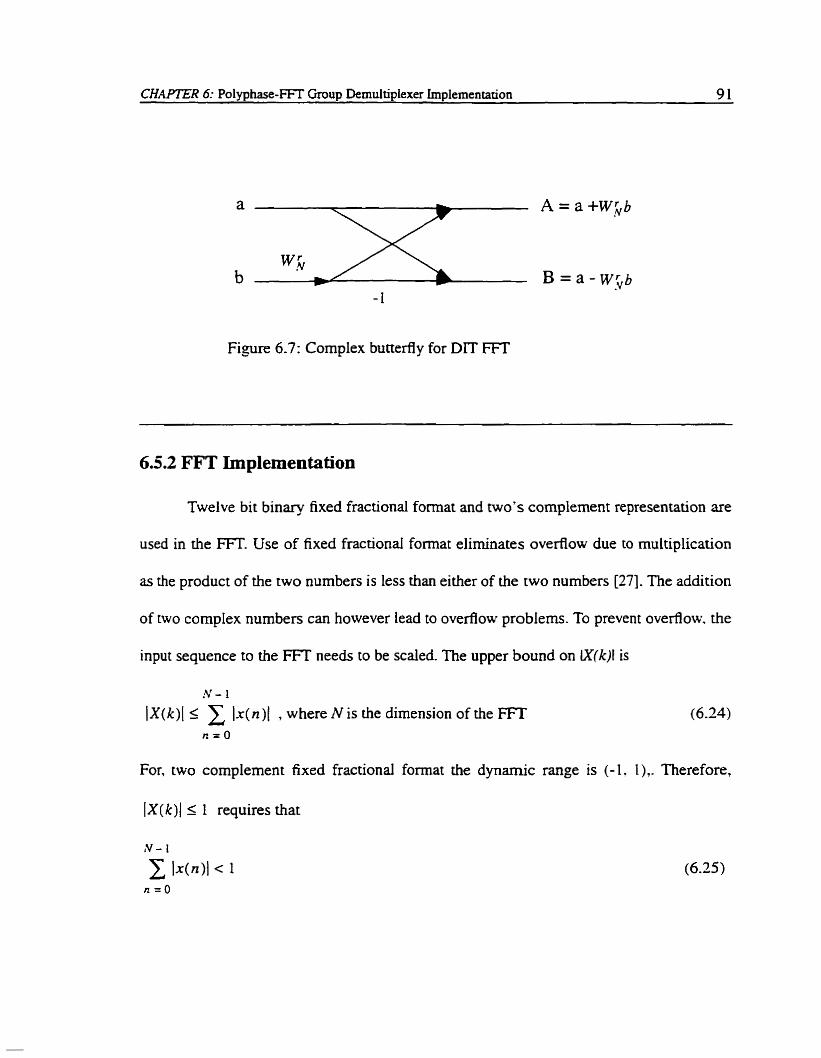
- 1
Figure 6.7: Complex butterfly for DIT FIT
6.5.2 FFT Implementation
Twelve bit binary fixed fractional format and two's complement representation are
used in the FFT. Use of fixed fractional format eliminates overflow due to multiplication
as the product of the two numbers is less than either of the two numbers [27]. The addition
of two cornplex numbers c m however lead to overflow problerns. To prevent overflow. the
input sequence to the FFI' needs to be scaled. The upper bound on IX(k)l is
N - 1
IX(k)l Ix(n)l , where N is the dimension of the FFT n = O
For, two complement fixed fractional format the dynamic range is (-1. I),. Therefore,
I X ( k ) 1 5 1 requires that

CHAPTER 6: Pol yphase-FFT Group DemultipIexer Implementation 92
For an FFT, there are two possible options to perform the scaling. In the first option
x(n) is initidly scaied such that Ix(n)l < 1 for al1 n. then each point in the sequence can
be scaled by N to ensure that Eq. 6.25 is satisfied. This scaling is ex*nnieIy severe and in
combination with the quantization errors gives a signai to noise d o (SNR) proportional
to N' [ t g ] . In the second option the total scaiing of IN can be distributed among the
stages of the FFï. By disvibuting the scaling of l / N uniformiy throughout the FFI' an
SNR that is inversely proportional to IN is obtained. The second option is used here to
keep the SNR proportional to N. The scaiing by 118 is distnbuted throughout the FFï
algorithm by scaling by 1/2 before each stage. The effects of the two methods of scaling is
not very pronounced for an 8-point FFT, however, for a larger FFT it is advisable to use
the second option for scaling.
In fixed-point arithmetic the addition of two numben does not require any trunca-
tion, provided overflow is avoided. Multiplication, however. does require tr~ncation. With
an 8-point FFT, the multiplication in the first two stages is by 1 and -j which is trivial and
does not require truncation. However. to maintain fixed word size, truncation is required in
,,-13 the third stage. The truncation errors occur in the final stages and range from (- - to O)
for each reai multiplication. The complex multiplien in the FFT use four real multipliers.
The variance of tnincation errors for each real multiplier is 2-24/ 12 and for the cornplex
multiplier it is /3 . Since these errors occur in the final stage they do not propagate

CHAPTER 6: f olyphase-FFT Group Demultiplexer Implementation 93
through the FFT. The multipliers are implemented by the add and shift rnethod, where the
shifts are hardwired. Simulation of the polyphase subfilters and phase shifters indicate that
their output Ix(n)l < 0.82 . Furthemore, this condition ensures that there is no overRow in
the complex buttedies in the final stage of the FTI:
DIT algorithm has been used for the implementation. For an 8-point EFï imple-
mentation both the DIT and the DIF Decimation-in-frequency) algorithrns use the sarne
number of multipliers and adders. The interfacing requirements for both the algorithrns,
however, are different.
The flow diagram of the &point FFT corresponding to Fig. 6.6 but with scaling in
each stage of the FFT is shown in Fig. 6.8. Because the scaling of 1/8 distributed through-
out the FFT, the output of the is 1/8 of its actual value. Referring to Fig. 6.8, it is
observed that a total of 12 butterfiies are used for the computation of the outputs. For the
first stage of the FFT the buttedies are identical. a single butterfiy is used for the firct
stage to perform al1 the operations, enabling reduction in number of logic modules. For the
second stage two buttedies are used. and for the third stage since al1 the butterflies require
diKerent twiddle factors, four different butterfiies are needed. Thus- by exploiting the
throughput capabilities of the hardwired complex buttertlies, it has k e n possible to reduce
the overall number of butterflies in the actual implementation of the FFT.
Figure 6.9 depicts the actual implementation of the J F T ' where 7 butterflies instead
of 12 are used. The FFT was implernented on four devices. Figure 6.10 shows the parti-

CHAPiER 6: Pol yphase-FFT Gmup Demultiplexer Implementation 94
S! 3 aD
*-
Cr,

C H ' R 6: Polyphase-FFï Group Demultiplexer Implementation 95

CHilPTER 6: Pol -pk-FFT Group Demultiplexer hplementation 96

CHAPTER 6: Po1 yphase-FFT Group Demultiplexer LmpIementatïon 97
tioning of the 8 point DIT. FFT on four devices. Stages 1 and 2 are implemenred on
devices la and lb and stage 3 is implemented on devices 2 and 3. Refemnj to Fig. 5.1. the
outputs from the FFI' are multiplied by (-1 .
653 FTT Implementation Resuits
The resufts for the implementation of the &point DR FFT are summarized in
Table 6.3, which depicts the device utiiization and the maximum operating frequency for
the implementation of the on the RH1280 and A1280 devices. The frequency of oper-
ation required for the first stage is 1/2 the system dock frequency, for the second stage it is
i/4 system dock frequency and for the third stage it is 1/8 the system clock frequency.
Consistent with these requirements. each input data sarnple is available for two dock
cycles.
Similar to the polyphase subfilters, the functionality of the FFT was tested through
simulations under worst. typical and best operating conditions with a system clock of 24
MHz. However, as indicated by the Acte1 static timing analysis, the FFT processor is Capa-
ble of operaûng at system clock 38 MHz for the RH1280 dcvices and 53 MHz for the
A 1280XL devices for the worst case operating conditions. The latency through the EW' is
34 system clock cycles.

C ' P T E R 6: Polyphase-FFI' Gmup DemuItipIexer Implementation 98
Table 6.3: Device utilization and delay for the 8-point, 12 bits input,output (complex) DIT-FFï
Die
RH 1280
A1280XL
Devicc Utilizarion SEQC,rn?UL LOGiC -
SEQtrPrrUt
Maximum rrgrster to q m c r DELAY in ris
30.0 52.9 (33.33) (18.90)
stage 1 stage2
(2 1 .Oû) ( 13.07)
25.3 43.5 (39.52) (22.37)
stage 1 stage2 39.8 64.1
(25.22) (15.60)
stage 3 203 -2 (4.92)
. -
stage 3 169.9 (5.88)
131.5 (8.2 1)
stage 3 174.5 (5.73)
125.0 (8.0)
- -
stage 1 stage2 11.6 21.8 86.20) (45.87)
12.3 22.0 8 1.30) (45.45)
stage 1 stage2 13.4 21.5 '74 -62) (46.5 1 )
13.0 22.4 '76.92) (44.64)
stage 3 57.4
( 17-42)
60.0 ( 16.66)
stage 3 58.7
(I7.W)
6 1.3 ( 16-28)

CHAPTER 6: Poiyphase-FFT Group Demultiplexer irnplementation 99
6.6 Rate Conversion Filter
The output from the demultiplexer is at the rate f, and needs to be converted to the
symbol rate f in order to be processed by the demodulator. This funcuon is performed by
the rate conversion filter. The rate conversion filter implemented here is a representative
filter. In an actual implementation, an adaptive rate control filter is used to adjust the tim-
ing sample sequence output by the demultiplexer and convert it to a baud rate sequence.
6.6.1 Rate Conversion Fiiter Coefficients
The coefficients for the rate conversion filter were derived using the Matlab based
software developed at the CRC [18]. The design method is the same as rhat used for the
polyphase subfilters. The parameren chosen for the rate conversion filter are listed in
Table 6.4. A list of the filter coefficients is provided in the Appendix B.
6.6.2 Implementation of the Rate Conversion Filter
The rate conversion filter is implemented as an FR filter with 9 taps and 7 bits of
quantization for the filter coefficients. The filter coefficients are represented as integen
and are in 2's complement format. The input to the rate conversion filter is 12 bits repre-
sented in binary fractional 2's complement format and the output is truncated to 12 bits

CHAPTER 6: Polyphase-FFT Group Demuitiplexer hplementaùon 1 0
Table 6.4: Parameters for the rate conversion filters
1 Beta factor for the kaiser window l 2 1
Parameter
Norrnalized frequency spacing (Fs)
Rolloff factor for the raised cosine filter
1 Number of taps per filter l 9 1
Value
1.5
0.4
1 Number of bits per filter tap 1 7 1
Mndow used 1 Kaiser
and is also in binary fractional 2's cornplement format. The tnincation errors have a vari-
ance of 2-"/ 12. The inputs are cornplex and the filter coefficients are real. hence two fil-
ters are needed to generate the complex output.
The rate conversion filter is symmeuic. and hence it is implemented by grouping
the inputs which are multiplied by the same coefficients and then appropriately shifting
them to foxm the partial products which are added by CSA adders. A final stage of addi-
tion is needed to obtain the output. Figures 6.1 1 and 6.12 represent the implementation of
the rate conversion filter. Figure 6.11 gives the direct form realization of the filter which
can be represented as in Eq. 6.26

CHAPTER 6: Polyphase-FFT' Group Demultiplexer implementation 101

CHAPTER 6: Polyphase-rn Group Demuitiplexer Implementation 102
which cm be modified to
y = ( - ~ x ( x + x ~ ) ) + ( ~ x ( x ~ + x 7 ) ) + ( - 8 x ( x 2 + x 6 ) )
+ ( ( 1 2 x ( x 3 + ~ 5 j ) + ( 6 3 ~ ~ 4 ) )
This then results in the implementation given by Eq. 6.28
y = (-(x+x8)) shified 1 left + (x l tx7) shifted 1 left + (-(x2+x6)) shifted 3 leh)
+ (x3+x5) shifted 3 ieft +(x3+x5) shifted 2 left + (x4 shifted 6 left) L-
partial product
+ sum 1
Partial products generated by shifting the sums I I
ddition of partial products using Carry Save Adders
i Output
\ delay
Figure 6.12: Block diagram for the implementation of the rate conversion filter

CHAPTER 6: Polyphase-FFT Group Demultiplexer Implementation 1 03
6.63 Rate Conversion Filter Implementation Resuits
The results for the implementation of the rate conversion filter in t e m of the
device utilization and the speed of operation are presented in Table 6.5. Each channel uses
two rate conversion filters. one for the real input and another for the imaginary input.
Hence, the total number of rate conversion filters used is 16 which were implemented on
eight ACTî devices. The functionaiity of the rate conversion filter is tested at 24 MHz sys-
tem clock and 3 MHz for the filter. However. the devices are capable of operating at sys-
tem clock rates of 38 MHz for the RH 1280 and 56 M H z for the A1 28OXL device.
The rate conversion filters for al1 the channels are similar. However, a different
decode circuit is used for each of the channels to conectly route in the data samples. This
has resulted in slight variations in the device utilization. The latency through the rate con-
version filter is 12 system clock cycles.
Table 6.5: Timing and device utilization for the two rate conversion filters (real and quadrature) on a single device
Die No. of 10s UStd
54
!+kimum regsur to regmer deiay m ns (rnuency) MHz
w o m case
206.3 (4.85)
typicai case
173.0 (5.78)
kstcye
58.1 (17.21)

CHAPTER 6.- Polyphase-FET Group Demultiplexer hplementation I O 4
6.7 Conclusion
This chapter discussed in detail the implementation of the building blocks of the
moup demultiplexer. Resulü for each implementation were also presented. From the c.
results it can be deduced that it is feasible to impiement the eight channei group demulti-
plexer using a reasonable number of FPGA devices and at the required system operating
frequenc y.
The results of the static timer tool from Actel indicate that the group dernultipiexer
is operational for a system dock of 38 MHz for the RH1280 and 53 M H i for the
A 1 28OXL devices. Higher throughputs can be ac hieved by utilizing arithrnetic cells whose
architectures inherently provide better performance through the use of cany look ahead
circuitry and pipelining. Also, identifying the cnticai slow nets and rerouting the design to
ensure minimum routing delays in the critical paths will result in higher throughputs.
However, such changes can only be achieved at the cost of higher gate counts and possibly
a larger number of devices.

CHAPTER 7: Summary and Further Research and Development
CHAPTER 7
Summary and Suggested Further Research and Development
An 8channel. Tl rate, group demultiplexer was implemented on the radiation-
hardened Actel FPGAs. It is the first time. reported in the lirerature. that an entire sub-
system such as the group demultiplexer has been implemented on radiation-hardened
Actel FPGAs. The design is fully operational for T 1 data rates and can aiso operate at E 1
data rates. The work presented in this thesis is in the framework of the research being car-
ried out at the CRC and CITR, on OBP technologies.
Architectures for the building blocks of the polyphase-FFï group demultipiexer:
polyphase subfilters and the FFT processor were optimized and implemented on the Acte1

CHAPTER 7: Summaxv and Further Research and Develo~ment 1 06
A m 2 devices. For DSP applications the speed of the arithrnetic module is of prime
importance. Various architectures for the arithmetic modules. which f o m an integd part.
of the building blocks of the demultiplexer. were considered. To limit the implementaùon
of the group dernultiplexer to a minimum number of devices. a trade-off between the
speed of operation and the gate count was made. Working with the desired speed. an
implementation which results in the minimum number of logic modules was used. For
multiplication, the add and shift multiplier was found to be the most efficient. The choice
of adden depended on their desired speed of operation. Wherever possible, low speed np-
ple adders were used to keep the numbcr of logic modules to a minimum.
The polyphase-FFT group demultiplexer with 8 bit input resolution and 12 bit out-
put resolution was implemented on twelve Actel RH 1280 and A 1280XL devices and the
rate conversion filters on eight devices. The circuit was tested for functionality under
woat. typical and best case operating conditions using Quicksim simulator tool from
Mentor Graphies. The maximum frequency of operation and the device utilization for the
devices were computed using Actel tools. The input and output delay information neces-
sary for proper interfacing between the devices was also provided. Static timer analysis
indicates that the group demultiplexer is operational for a system clock of up to 38 MHz
for RH1280 devices and 53 MHz for the A1280XL devices. The present design can oper-
ate with channel separations of up to 4.75 MHz for RH1280 devices and 6.6 MHz for the
A1280XL devices, which indicates that the design is also capable of operating at El rates.

C M R 7: Summary and Further Research and Development 1 07
The designs were mapped on to the A1280XL devices. The results from the testing
of the devices indicate that the cunent consumption per device is approximately 27 &i at
3.3 V and 43 rnA at 5 V for the polyphase subfilten and phase shifiers. Also. if multichip
modules (MCMs) are used, the power consumption will drop by approximately 158.
7.1 Further Research and Development
In diis thesis an 8-channel group demultiplexer was implemented on Acte1
RH1280 and A1280XL FPGAs. In the future it may be necessary to implement a group
demultiplexer with a larger number of channels. The increase in the number of channels
will require an extension of the current design and some modifications to it. The polyphase
network can be modified to accommodate a larger number of channels by using extra
devices for the channels which are added. Aiso. using the address to route the input data to
the polyphase subfilters from the ND converter makes it possible to extend this architec-
ture to incorporate larger number of channels. The number of devices required for the
implementation will increase as the number of channels increase.
Increasing the number of channels will require an FFT processor with a larger
number of points, since the size of the FFT processor is proportional to the numbers of
channels in the group demultiplexer. As the order of the FFI' becomes larger, the twiddle
factors for the buttedies will becomes more complex, thus placing a lot of emphasis on
the design of the multiplien. Pipelining within the multiplier to ensure desired speed of

CHAPTER 7: Simimary and Further Research and Development 108
operation would be a viable solution. An interesting option or possibility would be to corn-
bine 8-point l33"s to yield a larger F'Fï. For larger FFTs. quantization errors inuoduced in
die initial stages propagate to the final buttedies: hence their effects become more severe.
Techniques to keep the usage of CLB's as low as possible will have to be considered.
Much work needs to be done on the implementation of the adaptive rate conversion
filters. The present implementation is a representative filter indicating the complexity of
the filter coefficients. In an actual implementation, a set of filters needs to be stored and
decisions made by the timing and recovery algorithm will indicate the filter to be used.
The present implementation was on the Actel RH 1280 and A l28OXL device. The
results of the work presented here indicate the potential and the limitations of implement-
ing DSP hardware, such as the group demultiplexer, with the currently available 8k radia-
tion-hardened devices. In view of the fact that twelve devices were required to achieve
this, it is clear that a greater level of integration would be desirable. In the near future rad-
hard FPGA's with 20k gates are to be innoduced. Importing the design onto Iarger devices
will enable the use of lesser number of devices to implement the same design, reducing
considerably the interfacing requirements between the devices. As an example, the entire
8-point DIT FFT cm be implemented on a single Actel A32400DX device with 40k gates.
The viability of the FPGA technology will improve as the levels of integration are
enhanced-

References
References
1. Chun Loo, Steve Blostein. Tad Kwasniewski. Tho Le-Ngoc. David Plant, Valek Szwarc. "On Board Processing Techniques for Broadband Satellite Communications", 4th European Conference on Satellite Communications. Rome. Italy, pp. 50-55. Nov. 1997.
2. Kenny K. Hung, "Design and Test of a Regenerative Satellite Transmultiplexei'. Mas- ters Thesis Report, Queen's University, May 1993.
3. Fumio Takahata Masayuki Yasunaga Yasuo mata, Tomoki Ohsawa and Junji Narniki. 'A PSK Group Modem Based on Digital Signal Processing: Algorithm, Hardware Design. Irnplernentation and Performance", International Journal of Satellite Commu- nications, vol. 6, pp. 253-226, 1988.
4. Helmet Scheuennann and Heinz Gockler. "A Comprehensive Survey of Digitai Tram- multiplexing Methods". Proceedings of the IEEE, vol. 69, no. 11. pp. 1419-1450. Nov. 1981.
5 . Maurice G. Bellanger and Jacques L. Daguet. "TDM-FDM Transmultiplexer: Digital Polyphase and Fm'. IEEE Transactions on Communications, vol. COM-22. no. 9. pp. 1 199-1 974. Sept. 1971.
6 . T. Tsuda S. Monta and Y. Fujii. "Digital TDM-FDM Translator with Multi-Stage Stmcnire". IEEE Transactions on Communications. vol. COM-26, pp. 734-741. May 1978.
7. H. Gockler and H. Eyssele, "Study of On-Board Digital FDM-Demultiplexing for Mobile SCPC Satellite Communications". IEEE Transactions on Curnmunications. 1989.
8. Soheil 1. Sayegh, Francios T. Assalard and Thomas Inkai. "On-Board Rocessing Archi- tectures and Technology", IEEE Eascon 88 Proceedings, Arlington. VA, pp. 217-223. Nov. 1988.
9. S. Sayegh, M. Kappes. J. Thomas, J. Synder, M. Eng, J. Poklemba, M. Steber, and G. House, "An Overview of COMSAT Work in Multicarrier Demultiplexer/Demodula- ton". AIAA 14th International Communications Satellite Systems Conference and Exhibit, Washington, DC, pp. 1234- 1244, March 1992.

10. E. Del Re, P.L. Erniliani: "An Analytic Signal Approach for Transmultiplexers: Theory and Design", IEEE Transactions on Communications, vol. COM-30, no. 7. July 1982.
1 1. Fulvio Ananasso and Enrico Dei Re, 'Techniques and Technologies for Multicarrier Demodulation in FDMA/TDM Satellite Systerns", 3rd Tirrenia International Work- shop on Digital Cornrnunications, Tirrenia, Italy, Sepniber 1987. in Satellite Inle- grated Communications N e ~ o r k , E. Del Re. P. Barthelorne. and P.P. Nuspl, editors. Elsevier Science Publishen, Amsterdam. pp. 243-25 1, 1 988.
12. Enrico Del Re and Romano Fantacci, "Alternatives for On-Board Digital Multicarrier Demodulation". International Journal of Satellite Communications. vol. 6. pp. 267- 281, 1988.
1 3. L.R Rabiner and B. Gold, Theory and Applications of Digital Signal Processing, Prentice Hall, Eagiewwd Cliffs. New Jersey, 1975.
14. A. V, Oppenheim and R.W. Schafer, Discrete-Tnne Signal Processing, Prentice Hall, Eaglewood Cliffs, New Jersey, 1989.
1 5. S. J. Campanella and S. Sayegh, "A Flexible On-Board Demultiplexer/Demodulator'T, AIAA 12th International Communications Satellite Systems Conference, .klington. VA. pp. 299-303, March 1988.
16. W.H. Yim, C.C.D. Kwan, F.P. Coakley and B.G. Evans, "Multi-Carrier Demodulators for On-Board Processing Satellites", International Journal of Satellite Communica- tions, vol. 6, pp. 243-25 1, 1988.
17. N.P. Secord, "'Analysis of Interference Effects in Satellite On-Board Regenerative Repeaters", CRC Technicai Memorandum # CRC-RP-96-002, April 1996.
18. NP. Secord. "Frelirrinary Analysis of Quantization Effects in a Digital Group Demod- ulator", CRC Technical Memorandum VPCS #23/96, Oct, 1996.
19. Floyd M. Gardner, "Interpolation in Digital Modems-Part 1: Fundamentals". EEE Transactions on Communications, vol. 41, no. 3, pp. 50 1-507, March 1993.
20. FPGA Data Book and Design Guide, Actel Corporation, 1996.
2 1. Introduction tu Actel FPGA Architecture. Application note, Actel Corporation. 1996.

22. Jonathan Rose, Abbas El G d . Alberto Sangiovanni-Vincentelli, "'Architecture of Field Programmable Gate Arrays", Proceedings of the IEEE, vol. 8 1, no. 7. pp. 10 13- lO29. July 1993.
73. Radiation-Hardened Field Programmable Gate A r r q s . Mvanced Information. Ac tel Corporation.
24. G.C. Messenger and M.S. Ash. The Effects of Radiation on Electronic Sysrems. Van Nostrmd Reinhold Company Inc.. 1986.
25. John Rhea, "The Challenges of Space on the New COTS Frontier". Milit- and Aero- space Electronics, pp. 14- 18, May 1997.
26. GenesilKSOS4 Radiation Hardened CMOS/SOS Library wirh Silicon Compiler Design System. Hanis Serniconductor, May 199 1
27. Nan V. Oppenheim and Clifford J. Weinstein, "Effects of Finite Register Length in Digital Filtenng and the Fast Fourier Transfom", Proceedings of the IEEE. vol. 60. no. 8. pp. 957-976, Aug. 1972.
28. Proakis and Manolakis, Digital Signai Processhg, Principles. Algorithmr, and Appli- cations. Prentice Hall, New Jersey, 1996.
29. tlcrel Designer Ser-ies Developrnent Guide, Acte1 Corporation. 1 996.

Appendix A
Table Al: Timing information for the input and output for the devices p l to p8
Channel #
( 1 ) Macro INBLT (input buffer) (2) Macro TBHS (tristate output buffer)
Die
RH1280(i)
Input delay (ns)( ) wont .pical best case case case
12.6 10.5 3.5
Output delay(n~) (~) worst tvpical besr case case case
24.8 20.7 7.0

Table A 2 Timing information for the input and output for the FFï devices fla, flb, f2 and f3
Input delay (ns)(,) Output delay (ns)(?) worst typicd best worst typical best case case case case case case
Device #
( 1 ) Macro INBUF (input buffer) (2) Macro OUTBUF (output buffer)
Device

Table A3: Timing information for the input and output for the eight devices of the rate conversion tilters
Channel ff Device Input delay ( n ~ ) ( ~ , worst typical best case case case
Output delay (ns)(?) worst typical best case case case
( 1) Macro INBUF (input buffer) (2) Macro OUTBUF (output buffer)

Appendix B

Table B2: List of phase shifter multipüers
1 Channel # / Multiplier 1 ( a + jb) x multiplier
I - J E / 8 1 (acos n /8 + bsin x /8 ) + j(bcos n/8 -asin rc/8 )
(acos r / 4 + bsin n/4 ) + j(bcos n / l -asin x / l )
(asin n/8 + bcos n/8 ) + j(bsin n/8 -acos 7r/8 )
e -iJ./8 1 (-asin n/8 + bcos 7t/8 ) i j(-bsin n/8 -acos x / 8 )
7 1 - j 6n /8 1 (-acos 1[/4 + brin 11/4 ) + j(-kos n / 4 -asin ~ 1 4 )
where cos3n/8 = s inW8 , s i n 3 ~ / 8 = cosn/8
cosSx/8 = -sinx/8 . s i n 5 ~ / 8 = cos1V8
cos3x/4 = -cosx/4 , sin31t/4 = sinn/4
cos7x/8 = -cosn /8 , s i n 7 ~ / 8 = sinx/8
8 e
- i 7 ~ / 8 (-acos rc/8 + bsin 11/23 ) + j(-bcos x / 8 -asin ~ / 8 )

Table B3: Coefficients for the rate conversion filter
1 Tapno. 1 Coeff. 1

Appendix C
Raised-Cosine Filter
The raised-cosine fiiter has a frequency response H R C ( u ) given by
where o is the frequency in rads T is the baud period and W = r / T is the minimum
Nyquist bandwidth. The parameter P is called the roll-off factor which is the excess band-
width divided by the minimum Nyquist bandwidth. Figure C.1 shows the frequency
response of the raised-cosine filter for different values of B . For B = 0. the filter character-
istic corresponds to the ideal low-pas filter. For fl = 1. the response is known as full-
cosine roU-off characteristic which has bandwidth equal to twice the Nyquist bandwidth.
The impulse response of the raised-cosine filter is

which is depicted in Fig. C.2. From Fig. C.2. it is clear that the amplitudes of the oscilla-
tory tails of hRC(r) are smaller when B is large. This results in lower intersymbol inter-
ference. but higher excess bandwidth.
Figure C. 1 : Frequency response of raised-cosine filter for different roll-off factors
Figure C.2: Impulse response of raised-cosine filter for diff~rent roll-off factors

IMAGE EVALUATION TEST TARGET (QA-3)
APPLIEO A IMAGE. lnc E 1653 East Main Street - -. , Rochester. NY 14609 USA --
.L== Phone: 71 61482-0300 -- -- - - Far: 71 61288-5989
O 1993. Applied image. inc. Al1 Righis Resened