design and comparison of si-based and sic-based three
TRANSCRIPT

University of Wisconsin MilwaukeeUWM Digital Commons
Theses and Dissertations
August 2015
Design and Comparison of Si-based and SiC-basedThree-Phase PV InvertersWei FuUniversity of Wisconsin-Milwaukee
Follow this and additional works at: https://dc.uwm.edu/etdPart of the Electrical and Electronics Commons
This Thesis is brought to you for free and open access by UWM Digital Commons. It has been accepted for inclusion in Theses and Dissertations by anauthorized administrator of UWM Digital Commons. For more information, please contact [email protected].
Recommended CitationFu, Wei, "Design and Comparison of Si-based and SiC-based Three-Phase PV Inverters" (2015). Theses and Dissertations. 950.https://dc.uwm.edu/etd/950
DESIGN AND COMPARISON OF SI-BASED AND SIC-BASED THREE-PHASE PV
INVERTERS
by
Wei Fu
A Thesis Submitted in
Partial Fulfillment of the
Requirements for the Degree of
Master of Science
in Engineering
at
The University of Wisconsin-Milwaukee
August 2015
ii
ABSTRACT
DESIGN AND COMPARISON OF SI-BASED AND SIC-BASED THREE-PHASE PV
INVERTERS
by
Wei Fu
The University of Wisconsin-Milwaukee, 2015
Under the Supervision of Professor Robert M. Cuzner
The opportunities for both power density and efficiency improvements of photovoltaic (PV)
inverter have come with the development of commercially available wide bandgap (WBG)
devices such as Gallium Nitride (GaN), and Silicon Carbide (SiC).
In this thesis, how the replacement of Silicon (Si) Insulated Gate Bipolar Transistor (IGBT),
with SiC Metal-Oxide-Semiconductor Field Effect Transistor (MOSFET) affects the
power density and efficiency of a solar inverter implementation is presented. The focus is
on achieving a minimum volume of the output filter which meet the current harmonic
performance of IEEE standard, while meeting the thermal constraint of the semiconductor
device. Efficiency improvements are also characterized through an accurate calculation of
device and magnetic component losses—the largest contributors to loss in the system.
MATLAB/Simulnk and PLECS are used to assist in the process. Simulation is used to
calculate the differential mode pulsed voltages so that the required attenuation of the filter
can be determined and to determine the maximum switching frequency at which the device
can operate for a given heatsink design. Thus the power density can be compared. At the

iii
same time, by using the same filter but changing out devices, the efficiencies at the same
power density can be compared.
According to the results, when both use the maximum junction temperature as the
constraint, SiC-based inverter can operate at a much higher switching frequency, which
leads to a significant decrease in filter components and resulting a higher power density
than Si-based inverter. When operating at the same switching frequency, which means
keeping the power density the same, SiC devices leads to an improvement in efficiency.

iv
© Copyright by Wei Fu, 2015
All Rights Reserved
v
TABLE OF CONTENTS
LIST OF FIGURES
LIST OF TABLES
ACKNOWLEDGMENTS
Chapter 1 Introduction ........................................................................................................ 1
1.1 Background ............................................................................................................... 1
1.2 Research Status ......................................................................................................... 4
1.2.1 PV System .......................................................................................................... 5
1.2.2 Filter Design ....................................................................................................... 5
1.2.3 System Impacts of SiC Devices ......................................................................... 7
1.3 Research Objective and Article Layout .................................................................... 8
Chapter 2 LCL Filter Design ............................................................................................ 12
2.1 Literature Survey .................................................................................................... 12
2.2 LCL Filter Design Consider Volume ...................................................................... 14
2.2.1 Inductor Design ................................................................................................ 14
2.2.2 LCL Filter Design ............................................................................................ 19
2.2.3 Impact of Damping on LCL Filter Transfer Function ..................................... 21
Chapter 3 Thermal Circuit Calculation ............................................................................. 23
3.1 Thermal Circuit ....................................................................................................... 23
3.1.1 Concept of a Thermal Circuit........................................................................... 24
3.1.2 Thermal Circuit for Inverter ............................................................................. 25
3.1.3 Temperature Calculation .................................................................................. 27
3.2 Heatsink Design ...................................................................................................... 28
Chapter 4 Inverter Losses Calculation .............................................................................. 32
4.1 Calculation for Si Device Losses ............................................................................ 33
4.1.1 IGBT Loss ........................................................................................................ 34
4.1.2 Diode Loss ....................................................................................................... 38
4.2 Calculation for SiC MOSFET Losses ..................................................................... 43
4.3 Summary ................................................................................................................. 44
Chapter 5 Simulation Results and Analysis ...................................................................... 44
5.1 Description of the Simulation Model ...................................................................... 44
5.2 Si IGBT Based Inverter .......................................................................................... 48
5.3 SiC MOSFET Based Inverter ................................................................................. 52
5.4 Comparison of Si Based Inverter and SiC Based Inverter ...................................... 56
5.4.1 Power Density .................................................................................................. 56
5.4.2 Energy Efficiency ............................................................................................ 57
5.5 Summary ................................................................................................................. 58

vi
Chapter 6 Conclusion and Future Work ........................................................................... 59
6.1 Conclusion .............................................................................................................. 59
6.2 Future Work ............................................................................................................ 59
References ......................................................................................................................... 60

vii
LIST OF FIGURES
Figure 1-1 PV power generation system ............................................................................. 3
Figure 1-2 A conventional three-phase voltage-source inverter ......................................... 4
Figure 1-3 Three types of filter ........................................................................................... 6
Figure 1-4 Flow chart to obtain maximum switching frequency ...................................... 10
Figure 1-5 Flow chart to obtain energy efficiency ............................................................ 11
Figure 2-1 Outline of an inductor with core ..................................................................... 14
Figure 2-2 Inductor with air gap ....................................................................................... 14
Figure 2-3 Equivalent circuit of an inductor with air gap ................................................. 15
Figure 2-4 Magnetization curve for core material ............................................................ 16
Figure 2-5 Relationship between winding area and window area .................................... 17
Figure 2-6 Three views of the inductor............................................................................. 18
Figure 2-7 LCL filter without damping ............................................................................ 22
Figure 2-8 LCL filter with damping in series ................................................................... 22
Figure 2-9 LCL filter with damping in parallel ................................................................ 22
Figure 2-10 Bode plot of a LCL filter with and without damping .................................... 23
Figure 3-1 Thermal circuit for one device with heatsink .................................................. 24
Figure 3-2 Thermal circuit for a three-phase two-level inverter ....................................... 26
Figure 3-3 Package outline (a) .......................................................................................... 28
Figure 3-4 Package outline (b) .......................................................................................... 29
Figure 3-5 Module dimension ........................................................................................... 29
Figure 3-6 Inverter with heatsink ...................................................................................... 29
viii
Figure 4-1 Thermal description entrance for IGBT .......................................................... 34
Figure 4-2 Thermal description of IGBT (conduction loss) ............................................. 34
Figure 4-3 IC-VCE curve IGBT, output characteristic of IGBT (Inverter (typical)) .......... 35
Figure 4-4 Instantaneous conduction loss of IGBT .......................................................... 35
Figure 4-5 Thermal description of IGBT (turn-on loss) ................................................... 36
Figure 4-6 Thermal description of IGBT (turn-off loss) .................................................. 37
Figure 4-7 IC-E curve, switching losses characteristic of IGBT (Inverter (typical)) ........ 37
Figure 4-8 Instantaneous switching loss of IGBT ............................................................ 38
Figure 4-9 Thermal description entrance of Diode ........................................................... 39
Figure 4-10 Thermal description of Diode (conduction loss) ........................................... 39
Figure 4-11 IF-VF curve, forward characteristic of Diode (Inverter (typical)) .................. 40
Figure 4-12 Instantaneous conduction loss of Diode ........................................................ 40
Figure 4-14 Thermal description of Diode (turn-off loss) ................................................ 42
Figure 4-13 IF-E curve, switching losses characteristic of Diode (Inverter (typical)) ...... 42
Figure 4-15 Instantaneous switching loss of diode ........................................................... 43
Figure 4-16 Switching energy vs. temperature ................................................................. 44
Figure 5-1 PV system model............................................................................................. 45
Figure 5-2 Control part of PV system ............................................................................... 45
Figure 5-3 Third Harmonic Injection part ........................................................................ 46
Figure 5-4 Modulation waveforms of Third Harmonic Injection control ......................... 46
Figure 5-5 Waveforms of phase-neutral voltage .............................................................. 47
Figure 5-3 Inverter part of PV system .............................................................................. 48
Figure 5-4 Relationship between filter volume, capacitance and inductance (Si) ............ 49
ix
Figure 5-5 Waveforms of phase voltage, current and line-line voltage (Si) ..................... 49
Figure 5-6 FFT analysis of phase voltage and current without LCL filter (Si) ................ 50
Figure 5-7 FFT analysis of phase voltage and current with LCL filter (Si) ..................... 50
Figure 5-8 Losses of Si IGBT ........................................................................................... 51
Figure 5-9 Losses of Si Diode .......................................................................................... 51
Figure 5-10 Relationship between filter volume, capacitance and inductance (SiC) ....... 52
Figure 5-11 Waveforms of phase voltage, current and line-line voltage (SiC) ................ 53
Figure 5-12 FFT analysis of phase voltage and current without LCL filter (SiC) ........... 53
Figure 5-13 FFT analysis of phase voltage and current with LCL filter (SiC) ................. 54
Figure 5-14 Losses of SiC MOSFET (44kHz) ................................................................. 54
Figure 5-15 Losses of SiC Diode (44kHz) ....................................................................... 55
Figure 5-16 Losses of SiC MOSFET (7kHz) ................................................................... 55
Figure 5-17 Losses of SiC Diode (7kHz) ......................................................................... 56
x
LIST OF TABLES
Table 2-1 Current harmonic requirements ........................................................................ 20
Table 2-2 Voltage harmonic requirements ....................................................................... 21
Table 2-3 Capacitor table .................................................................................................. 21
Table 3-1 Fin spacing vs. fin length under different flow conditions ............................... 30
Table 3-2 Volumetric resistance vs. air flow condition .................................................... 32
xi
ACKNOWLEDGEMENTS
First of all I would like to express my heartfelt gratitude to my advisor Professor Robert
M. Cuzner for his patient guidance. I sincerely appreciate for all those discussions and
conversations in which Professor Cuzner shared his invaluable knowledge and experience,
and helped me to work out difficulties. I feel so lucky and blessed to have such a great
advisor who spears no effort to help students. I would like to specifically thank Professor
David C. Yu, for his support and encouragement to me, and for his effort to build up the
cooperative relationship between University of Wisconsin-Milwaukee and the universities
in China, which provide opportunities to students like me to study here. I would also like
to thank Professor Naira Campbell-Kyureghyan for her helpful comments on this work.
Special thanks as well to Professor Adel Nasiri for opening the door of power electronics
for me and his insightful ideas in my work.
Additionally, I want to thank my friends for their advice in my work and help in my life,
especially thank Qianqian Jiao and Ming Wang for their help both in my study and personal
life.
Finally, I would like to express my deepest appreciation to my family, for their
unconditional love and support, only with their love I can go so far to know more about the
wonderful world.
1
Chapter 1 Introduction
In this chapter, the background, research status, and general approach are presented.
1.1 Background
Due to the limitation of fossil resource, the rising costs of power energy, also for the issue
of protecting the environment, reducing the pollution emissions and preventing the global
warming, the cleanliness and sustainability of the renewable energy makes it more and
more important in today's world. As a kind of renewable energy, photovoltaic (PV) power
generation has been put into use for more than two decades, and solar PV energy installed
capacity over the past decade has risen rapidly. In 2006, the global solar PV energy
installed capacity was only 5 gigawatts (GW), while by the end of 2014, the stabilization
of solar power over the world was 177 GW according to literature [1]. Per reference [2],
the global solar PV energy installed capacity per year could increase to 200 GW by 2025.
Furthermore, the price is lower than ever due to the development of the related technology
such as the chip manufacturing process. Solar power has become the third most important
renewable energy after the hydro power and wind power.
A PV inverter, principally consists of a single phase or three phase voltage source inverter
circuit composed of high frequency switching power semiconductor devices, with
associated gate drives, DC link capacitance and low inductance laminated busbar, and
output filtering required to meet compatibility standards of the grid or distribution system
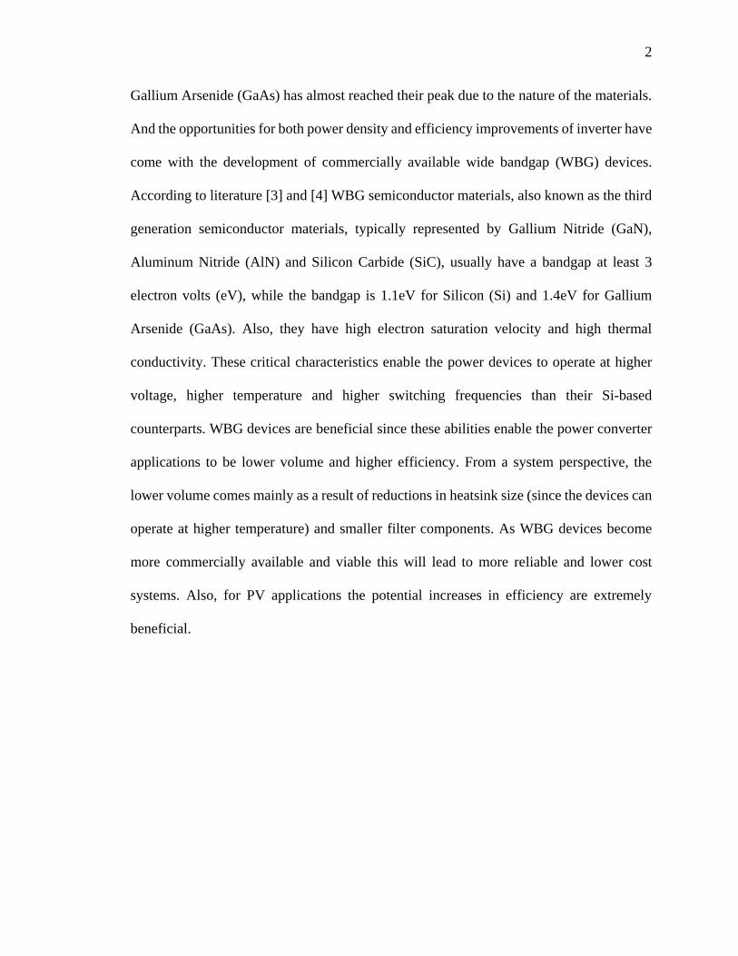
that it is feeding as shown in Figure 1-1. With the development of microelectronic
technology, the performance of conventional semiconductor such as Silicon (Si) and
2
Gallium Arsenide (GaAs) has almost reached their peak due to the nature of the materials.
And the opportunities for both power density and efficiency improvements of inverter have
come with the development of commercially available wide bandgap (WBG) devices.
According to literature [3] and [4] WBG semiconductor materials, also known as the third
generation semiconductor materials, typically represented by Gallium Nitride (GaN),
Aluminum Nitride (AlN) and Silicon Carbide (SiC), usually have a bandgap at least 3
electron volts (eV), while the bandgap is 1.1eV for Silicon (Si) and 1.4eV for Gallium
Arsenide (GaAs). Also, they have high electron saturation velocity and high thermal
conductivity. These critical characteristics enable the power devices to operate at higher
voltage, higher temperature and higher switching frequencies than their Si-based
counterparts. WBG devices are beneficial since these abilities enable the power converter
applications to be lower volume and higher efficiency. From a system perspective, the
lower volume comes mainly as a result of reductions in heatsink size (since the devices can
operate at higher temperature) and smaller filter components. As WBG devices become
more commercially available and viable this will lead to more reliable and lower cost
systems. Also, for PV applications the potential increases in efficiency are extremely
beneficial.
3
Charge
Controller
Load
GridMeter
Inverter
DC
ACBattery Bank
PV Array DC
DC
DC
AC
AC
Figure 1-1 PV power generation system
Nowadays, the most available switching device for high voltage and high power
application is the Si Insulated Gate Bipolar Transistor (IGBT), as the manufacturing
process of this kind of device is mature and cheap. However, this ubiquitous device has its
limitation due the Si material. The device junction temperature usually cannot go beyond
125℃ and the losses will be high in the high power applications—especially as the voltage
rating increases. As a result, for low voltage 480Vac applications the switching frequency
typically limited to 20kHz for low power applications (<50kVA) and 5kHz for high power
applications (>50kVA). The switching frequency directly impacts filter size and weight
which takes up the largest volume of the system for any system, such as a PV inverter,
where power quality and Electromagnetic Interference (EMI) standards must be met. Thus
the emergence of SiC-based devices which can operate at high temperature and have low
losses at much higher switching frequencies has attracted much attention in industries
where grid compatible power electronics are required. The SiC Schottky Barrier Diode
(SBD) has already been commercialized. These devices make up the reverse diode
component of the switches in Figure 1-2. The SiC SBD has a significant advantage of
4
having essentially a zero reverse recovery characteristic. Reverse recovery is a significant
contributor to switching losses in inverter circuits. The SiC Metal-Oxide-Semiconductor
Field Effect Transistor (MOSFET) is the most available type of SiC device to use as several
companies such as Cree, ROHM and APEI have launched SiC-based MOSFET for high
power application. They have extremely low power losses, can be operated at a high
junction temperature up to 250℃ if it has a well performed package and some of the devices
can be operated at a voltage up to 1700V, which means that they can be applied to low
voltage systems having voltage ratings as high as 690Vac.
FilterVin
Va
Vb
Vc
Ia
Ib
Ic
a
bc
DC AC
Figure 1-2 A conventional three-phase voltage-source inverter
According to [5] and [6], although some features of GaN are even better than SiC, the poor
quality caused by the immature manufacturing process, limits the commercialization of
GaN-based device. Therefore the emergence of these devices for practical applications is
trailing SiC, but it is promising as the next generation power semiconductor material.
1.2 Research Status
In this section, PV system will be briefly described, research status of the filter design and
system impacts of SiC-based devices will be presented.

5
1.2.1 PV System
As Figure 1-1 shows, PV power generation system is mainly composed of the PV array,
charge controller, battery bank, PV inverter, metering system and some other devices. It
can be operated in two modes: grid-tied mode and grid-forming mode. The PV inverter is
the application of power electronic technology in the field of solar power generation. It is
used to convert the direct current (DC) power generated by the solar battery into alternating
current (AC) power through the DC to AC inverter circuit, so that the power can be
supplied to the load or incorporated into the power grid. The PV inverter is the essential
and a core part of a solar PV power generation system. The usual circuit topology is a
voltage-source inverter (VSI) which is characterized by a capacitive energy storage, the
DC link capacitor bank, and power semiconductors that pass current in both directions but
only block voltage in one direction. The large majority of VSIs utilize IGBTs. The voltage
blocking limitation of IGBTs in the VSI circuit means that the peak AC voltages will
always be lower than the input DC link voltage. The efficiency of PV inverter is one of the
major factors that determines the solar array capacity and battery bank capacity. PV
inverter is a research focus in the PV power generation market as it plays a great role in the
PV system and has the most significant effect on the cost and efficiency of the system.
1.2.2 Filter Design
A conventional three-phase voltage-source inverter is shown as Figure 1-3. The filter is an
important part of the PV inverter. As previously mentioned, its size is the greatly impacted
by the operating frequency.

6
In Out In Out In Out
L L L1 L2
C C
(a) L filter (b) LC filter (c) LCL filter
Figure 1-3 Three types of filter
Generally, shown as Figure 1-3 there are three types of filter (single phase): (a) L filter,
contains only a filtering inductor, (b) LC filter, contains a filtering inductor and a capacitor,
(c) LCL filter, contains two filtering inductors and a capacitor. L filter and LCL filter are
the most commonly used type. LC filter is a 2rd-order filter, usually applied in inverters
which is working as an isolated source, its filtering effect is equal to LCL filter when it is
used in grid-connected inverter. Compared with L filter and LC filter, LCL filter has a
better performance in reducing the harmonics in VSI, especially the harmonics distortion
near the switching frequency. While design of LCL filter design is more complicated than
the design of L and LC types, and literatures mostly on the LCL filter.
References [7]-[18] are generally based on the same conditions and follow the procedures
which are proposed by Marco Liserre in [7] to decide the values of the passive components.
As described in the literatures, the basic conditions for the values of the inductance and
capacitance are according to the base values and resonant frequency of the filter, then based
on the required filter attenuation to decide the inductance and capacitance. The detailed
algorithm will be presented in section 2.1.
7
1.2.3 System Impacts of SiC Devices
In general, Si IGBT is always used in conventional PV inverters, but the emergence of
commercial SiC-based power transistors, especially SiC MOSFET, provides an alternative
for the switching device. Recently, much research has been done in applying SiC-based
device to PV system, such as in literature [19], [20] and [21].
Also, SiC-based and Si-based devices employed in PV system have been compared in
literatures, such as [22], [23], [24] and [25] which demonstrate that SiC-based devices have
lower losses. While SiC devices reduce the losses this is accompanied by higher di/dt and
dv/dt which have impacts on many aspects of the system design, such as stresses on the
insulation systems of any components that the SiC devices are switching against, impacts
on EMI and excitation of high frequency parasitic that exist within the LCL filter
components which can reduce the effectiveness of the filter if not taken into account in the
filter design stage. All of these considerations impact the packaging of the devices into the
system and this is the major area of emerging research in this field. Literature [26]
considered the loss versus EMI, and came up with a tradeoff of SiC-based and Si-based
devices.
What’s more, SiC devices enables reductions in the size of the thermal management system
and this will also come with improvements to energy efficiency which are also important—
especially to the PV system application. Reference [21], [22], [23], [27] and [28] discuss
the loss, thermal system management and efficiency improvement benefits of SiC-based
devices.
8
So far, SiC-based device is proved in literatures to have lower losses and can improve the
operating frequency of the inverter, thus the size of passive components can be greatly
reduced, which leads to lower costs of the PV system.
1.3 Research Objective and Article Layout
The main objective of this thesis is to compare how the replacement of Si IGBTs with SiC
MOSFETs affects the power density and efficiency of a solar inverter implementation. The
whole thesis can be described as development of a methodology which can provide two
rational indices, power density and energy efficiency, in order to compare the how an
application is enhanced through the upgrade to SiC devices
The first index is the power density. In this thesis, the main procedures to get the maximum
power density are described in Figure 1-4. From this flow chart, the maximum switching
frequency can be obtained. Since typically there is a negative correlation between the
volume of the inverter and the switching, the maximum power density of two kinds of
devices can be obtained from a maximum junction temperature constraint. The objective
of this exercise is to obtain the minimal possible volume for each of the designs being
considered—i.e. minimum volume that is possible with a solar inverter utilizing Si IGBTs
or SiC MOSFETs. Once the maximum switching frequency is determined, the minimum
filter size can be determined for the switching frequency given the inverter harmonic output
requirements. Design of the minimum filter size includes determination of the optimal
allocation of inductance and capacitance to the filter design with the following inputs and
constraints:

9
• Power rating
• Current limiting capability under a faulted condition
• Current controllability
• Minimization of filter component parasitic elements that are effected by operation
at the switching frequency
Since typically there is a negative correlation between the volume of the inverter and the
switching frequency, it is expected that the SiC-based inverter will have the greater power
density.

10
Start
Heat sink design
Thermal
resistance of
heat sink
Calculate inverter losses
from PLECS and according
to the filter design
Junction
temperature
Device
losses
Calculate junction
temperature
>Max junction
temperature ?
LCL filter design
considering volume
Increase switching
frequency
End
YES
NO
Figure 1-4 Flow chart to obtain maximum switching frequency
The other index is the energy efficiency. In this thesis, the main procedures to get the
energy efficiency are described in Figure 1-5. In this case, the larger volume design for the
power density index is selected and it provides the switching frequency. This volume will

11
be that of a Si IGBT based solar inverter designed to achieve a maximum power density
given temperature constraints. The efficiency of that design will then be calculated. This
will be followed by determination of the losses if the Si IGBTs were simply replaced by
SiC MOSFETs keeping the switching frequency and LCL filter design the same.
Start
Calculate inverter losses
from PLECS thermal model
Energy
efficiency
LCL filter design
considering volume
A certain
switching
frequency
End
Figure 1-5 Flow chart to obtain energy efficiency
In this thesis, a three-phase PV system with rated power of 200KVA, rated voltage of 480V
and DC link voltage of 750V is designed. According to the system requirements, Si IGBT
module FF300R12KT4 from Infineon and SiC MOSFET CAS300M12BM2 module from
Cree are chosen to be the switching device for the respective Si- and SiC-based designs,
since the operating voltage of these two devices is 1200V and the maximum current can
go beyond 400A which can ensure safe system operation.

12
There are 6 chapters in this thesis. Chapter 1 briefly introduces the background of this
research and the new progress in the area. Research objective and article layout are also
included in this chapter. Chapter 2 mainly explains the LCL filter design algorithm which
considered the volume the filter. It is the crucial basis for the latter part of the thesis.
Chapter 3 consists of thermal circuit and heatsink design. It provides the theoretical
foundation for the temperature calculation. Chapter 4 illustrates the calculation of inverter
losses, it is the crux part to get the final results. Chapter 5 is mainly composed of simulation
part and analysis part, furthermore, this chapter leads to the conclusion of this thesis which
is stated in chapter 6. Finally, Chapter 6 presents the conclusion and prospects the future
work.
Chapter 2 LCL Filter Design
2.1 Literature Survey
According to the literatures [7]-[18], the following are the basic conditions and procedures
for LCL filter design: 1. Base inductance and base capacitance are calculated according to
the fundamental frequency and rating values. 2. The inductance and capacitance values of
the filter are usually some percentage of the base values. Usually, the total inductance
should not exceed 12% of the base value, the capacitance should not exceed 10% of the
base value and start at 3% of the base value. 3. The converter side inductance L1 is
determined by the ripple current. And the grid side inductance L2, which is some percentage
of convert side inductance. L1/L2 ratio ranges from 2 to 7, and usually the ratio is equal to
3 for a good performance. 4. Resonance frequency of filter must avoid to be close to both
fundamental frequency and switching frequency, and it should be bigger than ten times of
13
fundamental frequency and smaller than half time of switching frequency. 5. The
capacitance can be increased by small steps and repeat steps 3 and 4, if the above conditions
cannot be met. Also, the ratio of L1/L2 can be adjusted if needed. 6. Choose the combination
of inductance and capacitance which have the highest attenuation at switching frequency
if there are various choices.
Based on these procedures, [8] used the attenuation of output current versus input voltage,
and analyzed the relationship of the inductor ratio, capacitor value and the harmonics
comprehensively. [9] added a damping resistor which is in series with the capacitor to avoid
the resonance at the switching frequency, the authors designed and implemented a filter for
a 5 kW three-phase grid-connected inverter, and test the filter in stand-alone mode. [10]
designed a filter for grid-connected neutral point clamped (NPC) inverter and compared L
filter with LCL filter by simulation with Simplorer. [11] compared the LCL filter with
damping resistor in parallel and damping resistor in series, and it showed that the filter with
damping in parallel has lower power loss. [12] applied the clonal selection theory into the
design of filter for PV system. [17] basically follows the steps above, but it decided the
sum inductance considering several other conditions including the reactive power
requirements and transient current tracking index.
Most of these papers took the same basic design steps, but they did not take into account
the practical combination of inductor and capacitor which lead to a minimum volume,
which is critical for the power density of the inverter.
14
2.2 LCL Filter Design Consider Volume
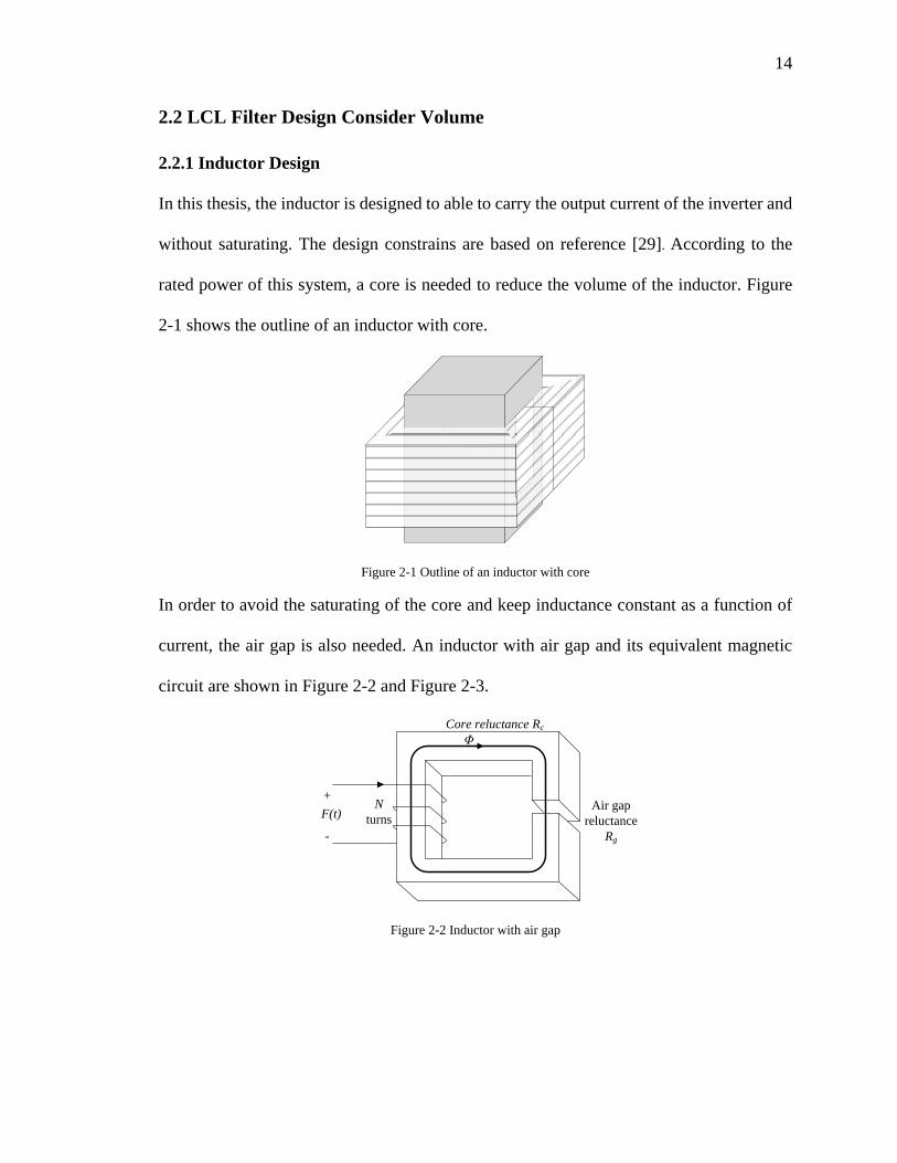
2.2.1 Inductor Design
In this thesis, the inductor is designed to able to carry the output current of the inverter and
without saturating. The design constrains are based on reference [29]. According to the
rated power of this system, a core is needed to reduce the volume of the inductor. Figure
2-1 shows the outline of an inductor with core.
Figure 2-1 Outline of an inductor with core
In order to avoid the saturating of the core and keep inductance constant as a function of
current, the air gap is also needed. An inductor with air gap and its equivalent magnetic
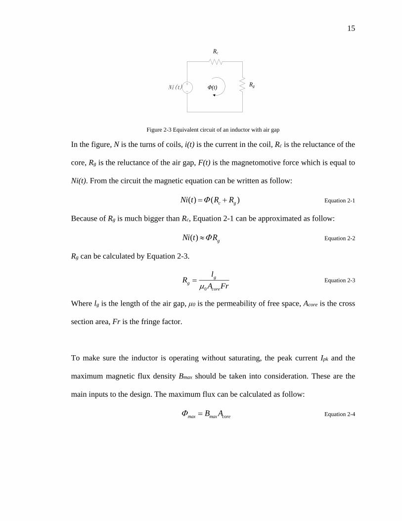
circuit are shown in Figure 2-2 and Figure 2-3.
+
-
F(t)N
turns
Φ
Core reluctance Rc
Air gap
reluctance
Rg
Figure 2-2 Inductor with air gap
15
Φ(t)Ni(t)
Rc
Rg
Figure 2-3 Equivalent circuit of an inductor with air gap
In the figure, N is the turns of coils, i(t) is the current in the coil, Rc is the reluctance of the
core, Rg is the reluctance of the air gap, F(t) is the magnetomotive force which is equal to
Ni(t). From the circuit the magnetic equation can be written as follow:
( ) ( )c gNi t R R Equation 2-1
Because of Rg is much bigger than Rc, Equation 2-1 can be approximated as follow:
( ) gNi t R Equation 2-2
Rg can be calculated by Equation 2-3.
0
g
g
core
lR
A Fr Equation 2-3
Where lg is the length of the air gap, μ0 is the permeability of free space, Acore is the cross
section area, Fr is the fringe factor.
To make sure the inductor is operating without saturating, the peak current Ipk and the
maximum magnetic flux density Bmax should be taken into consideration. These are the
main inputs to the design. The maximum flux can be calculated as follow:
max max coreB A Equation 2-4

16
Figure 2-4 Magnetization curve for core material
For this application, the core is manufactured with iron based metglas. According to the
magnetization curve in Figure 2-4, the maximum flux density need to be under the
saturating flux density and is better to be at the linear part of the curve. 1.2Tesla is chosen
to be the maximum flux density. Replacing i(t) with Ipk, and substitute Equation 2-3 and
Equation 2-4 into Equation 2-2, the design should satisfy the constrain as follow:
0
g
pk max core
core
lNI B A
A Fr Equation 2-5
Rearranging Equation 2-5, N can be calculated by:
0
g
max
pk
lN B
FrI Equation 2-6
The inductor should also be designed to have a certain inductance L, and the inductance L
can be calculated by:
2
g
NL
R Equation 2-7
For a specified inductance, and substituting Equation 2-3 and Equation 2-6 into Equation
2-7, Acore can be obtained as follow:
17
2
0
2
pk
core
max g
LI FrA
B l
Equation 2-8
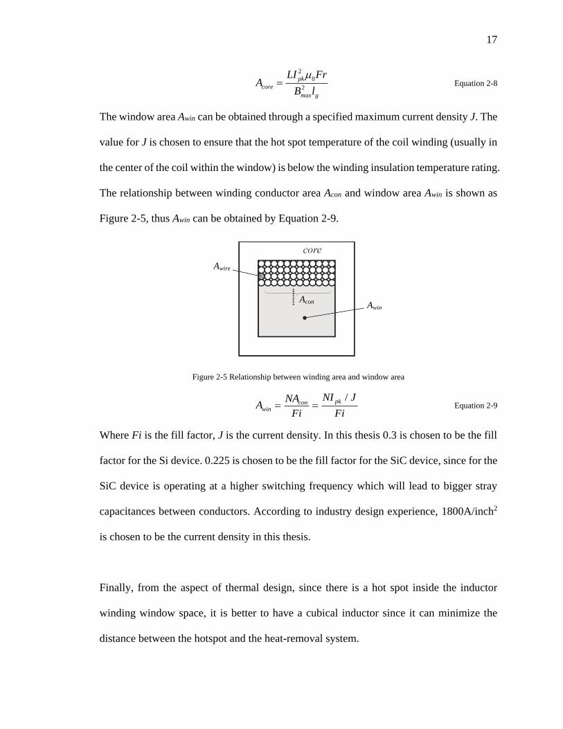
The window area Awin can be obtained through a specified maximum current density J. The
value for J is chosen to ensure that the hot spot temperature of the coil winding (usually in
the center of the coil within the window) is below the winding insulation temperature rating.
The relationship between winding conductor area Acon and window area Awin is shown as
Figure 2-5, thus Awin can be obtained by Equation 2-9.
AconAwin
Awire
Figure 2-5 Relationship between winding area and window area
/pkconwin
NI JNAA
Fi Fi Equation 2-9
Where Fi is the fill factor, J is the current density. In this thesis 0.3 is chosen to be the fill
factor for the Si device. 0.225 is chosen to be the fill factor for the SiC device, since for the
SiC device is operating at a higher switching frequency which will lead to bigger stray
capacitances between conductors. According to industry design experience, 1800A/inch2
is chosen to be the current density in this thesis.
Finally, from the aspect of thermal design, since there is a hot spot inside the inductor
winding window space, it is better to have a cubical inductor since it can minimize the
distance between the hotspot and the heat-removal system.

18
According to constrains above, the inductor can be designed. Figure 2-6 shows three views
of the inductor to have a clear look at the inductor dimensions.
a
cH
b
dx
W
x
L
aAwin
Acore
Figure 2-6 Three views of the inductor.
In Figure 2-6, H, W, L are the height, width and length of the inductor. Hence, the volume
can be calculated as:
Volume H W L Equation 2-10
From the geometry relationship, Equation 2-11 and Equation 2-12can be obtained.
2winA x c Equation 2-11
coreA a d Equation 2-12
Where Awin and Acore are from constrains described by Equation 2-8 and Equation 2-9. Since
it is a cubical inductor the height, width and length should be equal to each other:
H W L Equation 2-13
Expand Equation 2-13:
2 4 2c a x a Equation 2-14
19
4 2 2x a x d Equation 2-15
Therefore, the volume can be calculated by solving Equation 2-10~Equation 2-15.
Practically, there is a stacking factor that takes into account the spacing between
laminations in the d dimension. For this design, it is assumed to be 0.9 in this thesis. The
actual volume can be obtained by the volume calculated above divided by that stacking
factor.
2.2.2 LCL Filter Design
According to power rating, the combined procedures described above require a starting
point. Using the rated power PB, rated voltage VB and fundamental frequency fB, base
impedance ZB, base inductance LB and base capacitance CB can be calculated as follows:
2
Z BB
B
V
P Equation 2-16
2
BB
B
ZL
f Equation 2-17
1
2B
B B
Cf Z
Equation 2-18
The total inductance should not exceed 12% of base inductance of the base value, the
capacitance should not exceed 10%, however, the power factor can be actively controlled
if necessary, this would tempers this limitation, and L1/L2 ratio is 3.
In this design, the total inductance value, L1+L2, is constrained by the following:
• Resonant frequency:
1 2
1 2
1
2res
L Lf
L L C
Equation 2-19

20
10 0.5B res swf f f Equation 2-20
Where fB is the fundamental frequency, fsw is the switching frequency.
• Current limiting capability under a faulted condition:
max pkmax pkI I I Equation 2-21
2
3
DCmax swmin
max
V fL
I
Equation 2-22
Where Ipk is the peak current, and the Ipkmax is the peak current when a faulted occurs, VDCmax
is the maximum DC voltage.
• Current controllability:
The estimate range of capacitance value is 10~200uF. Because of the capacitors can only
be obtained from off the shelf parts, while the inductor can be custom designed to achieve
a minimum volume, the volumes of capacitors over the range of capacitance values are
chosen from actual components. These are used in combination with an iterative inductor
design process in order to determine the optimal values of inductance according to a
minimum total volume constraint and the required attenuations derived from IEEE519 and
IEEE1547 harmonic requirements shown in Table 2-1 and
Table 2-2. And volumes of C can be got from the datasheets as shown in Table 2-3.
Table 2-1 Current harmonic requirements
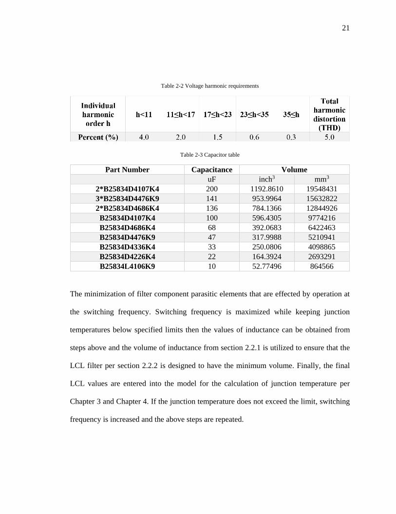
21
Table 2-2 Voltage harmonic requirements
Table 2-3 Capacitor table
Part Number Capacitance Volume
uF inch3 mm3
2*B25834D4107K4 200 1192.8610 19548431
3*B25834D4476K9 141 953.9964 15632822
2*B25834D4686K4 136 784.1366 12844926
B25834D4107K4 100 596.4305 9774216
B25834D4686K4 68 392.0683 6422463
B25834D4476K9 47 317.9988 5210941
B25834D4336K4 33 250.0806 4098865
B25834D4226K4 22 164.3924 2693291
B25834L4106K9 10 52.77496 864566
The minimization of filter component parasitic elements that are effected by operation at
the switching frequency. Switching frequency is maximized while keeping junction
temperatures below specified limits then the values of inductance can be obtained from
steps above and the volume of inductance from section 2.2.1 is utilized to ensure that the
LCL filter per section 2.2.2 is designed to have the minimum volume. Finally, the final
LCL values are entered into the model for the calculation of junction temperature per
Chapter 3 and Chapter 4. If the junction temperature does not exceed the limit, switching
frequency is increased and the above steps are repeated.

22
2.2.3 Impact of Damping on LCL Filter Transfer Function
The transfer function of LCL filter without damping (shown in Figure 2-7) is
3
1 2 1 2
1
( )LCLT
S L L C S L L
Equation 2-23
Out
L1 L2
CIn
Figure 2-7 LCL filter without damping
The transfer function of LCL filter with damping in series (shown in Figure 2-8) is
3 2
1 2 1 2 1 2
1
( ) ( )LCL
SCRT
S CL L S CR L L S L L
Equation 2-24
Out
L1 L2
CIn
R
Figure 2-8 LCL filter with damping in series
The transfer function of LCL filter with damping in parallel (shown in Figure 2-9) is
3 2
1 2 1 2 1 2( )LCL
RT
S CRL L S L L SR L L
Equation 2-25
Out
L1 L2
CIn R
Figure 2-9 LCL filter with damping in parallel

23
And in this thesis, paralleled damping resistor is applied since the high order harmonic
current through the capacitor is lower when the resistor is paralleled according to reference
[11], also a capacitance which equals to half of C is in series with damping resistor for EMI
issue. Figure 2-10 shows the bode plot of a LCL filter with and without damping.
Figure 2-10 Bode plot of a LCL filter with and without damping
It is clear that the resonance of the LCL filter can be well damped with the damping resistor,
and usually R can be obtained by Equation 2-26 for wye connection and three times of that
for delta connection.
1
6 res
Rf C
Equation 2-26
Chapter 3 Thermal Circuit Calculation
This section covers the principles behind the thermal circuit calculation.

24
3.1 Thermal Circuit
This section covers the thermal circuit concepts for the inverter application.
3.1.1 Concept of a Thermal Circuit
Before the thermal modeling, in order to get a clear understanding of the objective and
result of the PLECS model, the concept of a thermal circuit is necessary to be explained.
In an electrical circuit, applying Ohm’s low, Equation 3-1can be written as follow:
VR
I Equation 3-1
Where R is the resistance, △V is the voltage difference, I is the current. Thermal circuit is
analogous to electrical circuit and thermal resistance can be written as follow:
th
D
TR
P Equation 3-2
Where Rth is the thermal resistance, △T is the temperature difference, PD is the power
dissipation. Figure 3-1shows the thermal circuit and parameter relationships for one device
with heatsink.
Rth_SA
TA
TS
TC
TJ
Rth_CS
Rth_JC
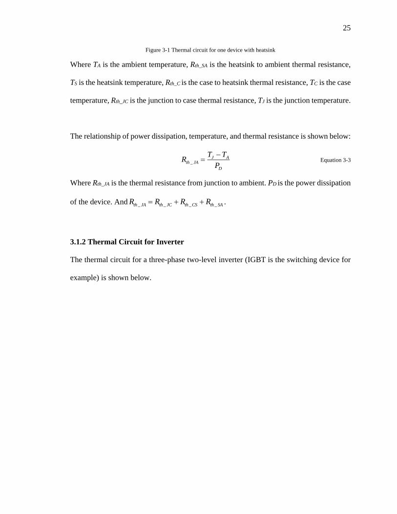
25
Figure 3-1 Thermal circuit for one device with heatsink
Where TA is the ambient temperature, Rth_SA is the heatsink to ambient thermal resistance,
TS is the heatsink temperature, Rth_C is the case to heatsink thermal resistance, TC is the case
temperature, Rth_JC is the junction to case thermal resistance, TJ is the junction temperature.
The relationship of power dissipation, temperature, and thermal resistance is shown below:
_J A
th JA
D
T TR
P
Equation 3-3
Where Rth_JA is the thermal resistance from junction to ambient. PD is the power dissipation
of the device. And _ _ _ _th JA th JC th CS th SAR R R R .
3.1.2 Thermal Circuit for Inverter
The thermal circuit for a three-phase two-level inverter (IGBT is the switching device for
example) is shown below.
26
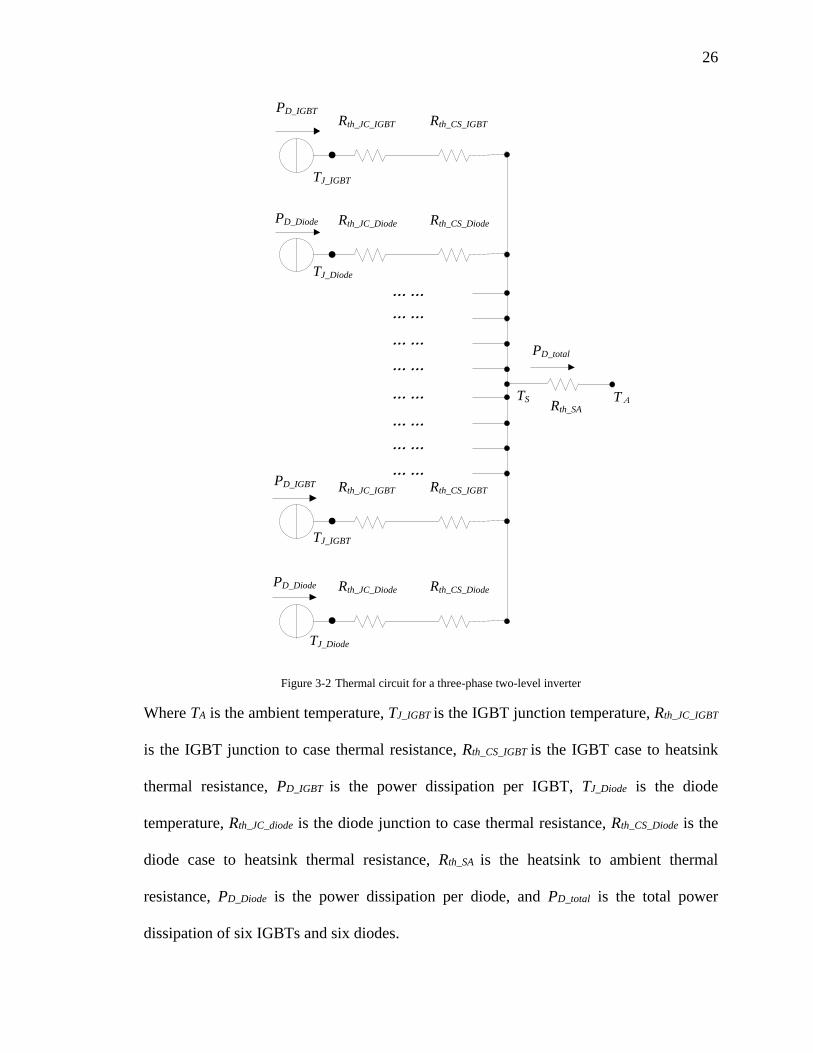
PD_IGBT
TJ_IGBT
Rth_JC_IGBT Rth_CS_IGBT
PD_Diode
TJ_Diode
Rth_JC_Diode Rth_CS_Diode
TJ_IGBT
Rth_JC_IGBT Rth_CS_IGBT
Rth_JC_Diode Rth_CS_Diode
TJ_Diode
… …
… …
… …
… …
… …
… …
… …
… …
TA
PD_total
TS
PD_IGBT
PD_Diode
Rth_SA
Figure 3-2 Thermal circuit for a three-phase two-level inverter
Where TA is the ambient temperature, TJ_IGBT is the IGBT junction temperature, Rth_JC_IGBT
is the IGBT junction to case thermal resistance, Rth_CS_IGBT is the IGBT case to heatsink
thermal resistance, PD_IGBT is the power dissipation per IGBT, TJ_Diode is the diode
temperature, Rth_JC_diode is the diode junction to case thermal resistance, Rth_CS_Diode is the
diode case to heatsink thermal resistance, Rth_SA is the heatsink to ambient thermal
resistance, PD_Diode is the power dissipation per diode, and PD_total is the total power
dissipation of six IGBTs and six diodes.
27
Each device can be handled as a current source in electrical circuit, junction to case thermal
resistance and case to heatsink thermal resistance for each device are in series, and all the
devices connected parallel to the heatsink. It should be noted that the temperature of IGBT
is not the same as the temperature of diodes. For each IGBT and diode, the thermal
equations can be written as follow:
_S A
th SA
total
T TR
P
Equation 3-4
_
_ _ _ _
_
J IGBT S
th JC IGBT th CS IGBT
D IGBT
T TR R
P
Equation 3-5
_
_ _ _ _
_
J Diode S
th JC Diode th CS Diode
D Diode
T TR R
P
Equation 3-6
3.1.3 Temperature Calculation
In this thesis, the device junction temperature is one of the key factors to restrict the power
dissipation capability, while the switching frequency and the characteristic of the device
are the factors that determine the power dissipation. This means for the same device, and
the other limiting conditions, the device junction temperature determines the switching
frequency.
To discover the temperature of the device, Equation 3-4, Equation 3-5, Equation 3-6 are
rearranged as follows:
_ _ _ _ _ _
_ _ _ _ _ _
J IGBT th JC IGBT th CS IGBT D IGBT S
th JC IGBT th CS IGBT D IGBT th SA total A
T R R P T
R R P R P T
Equation 3-7

28
_ _ _ _ _ _
_ _ _ _ _ _
J Diode th JC Diode th CS Diode D Diode S
th JC Diode th CS Diode D Diode th SA total A
T R R P T
R R P R P T
Equation 3-8
3.2 Heatsink Design
Equation 3-7 and Equation 3-8 can be used to determine the heatsink to ambient thermal
resistance. This thermal resistance dictates the size of the heatsink. To make sure the value
of thermal resistance is in a reasonable range, the heatsink design is expressed.
Si IGBT module FF300R12KT4 from Infineon and SiC MOSFET CAS300M12BM2
module from Cree are the same package. Their dimensions can be obtained from their
respective data sheets. Outline of FF300R12KT4 shown as Figure 3-3 and Figure 3-4 (all
units are in mm). The length of this module LC is 61.4 mm, width WC is 106.4 mm and
height HC is 30.9 mm as shown in Figure 3-5. The heatsink is designed to accommodate
these dimensions.
Figure 3-3 Package outline (a)
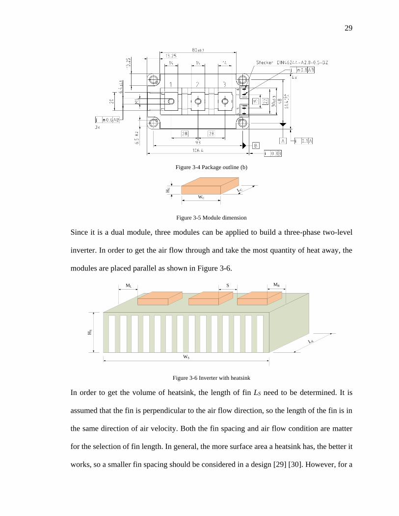
29
Figure 3-4 Package outline (b)
WC
HC
LC
Figure 3-5 Module dimension
Since it is a dual module, three modules can be applied to build a three-phase two-level
inverter. In order to get the air flow through and take the most quantity of heat away, the
modules are placed parallel as shown in Figure 3-6.
WS
HS
MLMRS
LS
Figure 3-6 Inverter with heatsink
In order to get the volume of heatsink, the length of fin LS need to be determined. It is
assumed that the fin is perpendicular to the air flow direction, so the length of the fin is in
the same direction of air velocity. Both the fin spacing and air flow condition are matter
for the selection of fin length. In general, the more surface area a heatsink has, the better it
works, so a smaller fin spacing should be considered in a design [29] [30]. However, for a
30
certain width of heatsink, smaller fin spacing means more fins, and that can lead to adverse
effects on pressure drops and flow bypass, and the average heat transfer coefficient goes
down [30]. Also for a higher fin density, the manufacturing process is more difficult, which
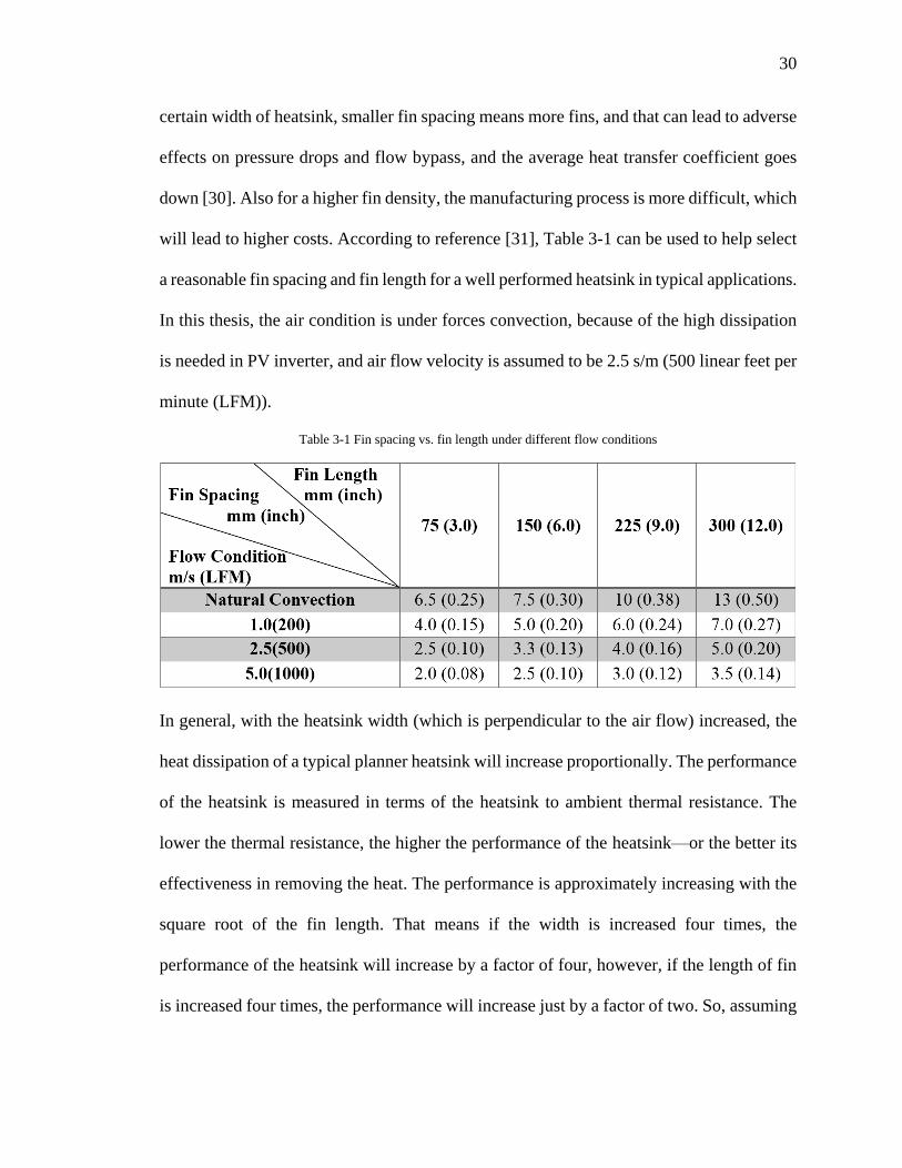
will lead to higher costs. According to reference [31], Table 3-1 can be used to help select
a reasonable fin spacing and fin length for a well performed heatsink in typical applications.
In this thesis, the air condition is under forces convection, because of the high dissipation
is needed in PV inverter, and air flow velocity is assumed to be 2.5 s/m (500 linear feet per
minute (LFM)).
Table 3-1 Fin spacing vs. fin length under different flow conditions
In general, with the heatsink width (which is perpendicular to the air flow) increased, the
heat dissipation of a typical planner heatsink will increase proportionally. The performance
of the heatsink is measured in terms of the heatsink to ambient thermal resistance. The
lower the thermal resistance, the higher the performance of the heatsink—or the better its
effectiveness in removing the heat. The performance is approximately increasing with the
square root of the fin length. That means if the width is increased four times, the
performance of the heatsink will increase by a factor of four, however, if the length of fin
is increased four times, the performance will increase just by a factor of two. So, assuming

31
the heatsink has a large enough surface area, it is more beneficial to increase the width of
the heatsink than increase the length.
The chips have to be on the surface area of heatsink. In this thesis, LC is 61.4 mm. So,
choosing 150 mm can be a good estimation to leave about half length of the chip to the
front and back margins. Correspondingly, the fin spacing of 3.3 mm look up from Table
3-1 is a reasonable value. Choosing the spacing S between chips, the left margin ML and
right margin MR equal to half length of the chip. The width of the heatsink WS is five times
of module width WC, that is 532 mm. And the height of a heatsink HS for inverter can goes
up to 300 mm. Therefore, 150 mm can be chosen for a reasonable performance.
The volume can be obtained from above procedures, then according to reference [32], the
thermal resistance can be obtained by the following equation:
_V
th SA
S
RR
V Equation 3-9
Where Rth_SA is the heatsink to ambient thermal resistance, VS is the heatsink volume, RV is
the volumetric resistance.
The rough ranges of volumetric resistance under different air flow conditions are given by
Table 3-2.
32
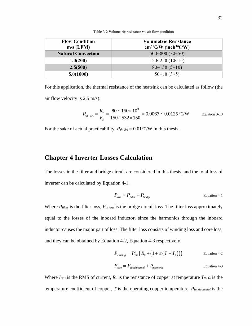
Table 3-2 Volumetric resistance vs. air flow condition
For this application, the thermal resistance of the heatsink can be calculated as follow (the
air flow velocity is 2.5 m/s):
3
_
80 ~ 150 100.0067 ~ 0.0125
150 532 150
Vth SA
S
RR
V
℃/W Equation 3-10
For the sake of actual practicability, Rth_SA = 0.01℃/W in this thesis.
Chapter 4 Inverter Losses Calculation
The losses in the filter and bridge circuit are considered in this thesis, and the total loss of
inverter can be calculated by Equation 4-1.
loss filter bridgeP P P Equation 4-1
Where Pfilter is the filter loss, Pbridge is the bridge circuit loss. The filter loss approximately
equal to the losses of the inboard inductor, since the harmonics through the inboard
inductor causes the major part of loss. The filter loss consists of winding loss and core loss,
and they can be obtained by Equation 4-2, Equation 4-3 respectively.
2
0 01winding rmsP I R T T Equation 4-2
core fundamental harmonicP P P Equation 4-3
Where Irms is the RMS of current, R0 is the resistance of copper at temperature T0, α is the
temperature coefficient of copper, T is the operating copper temperature. Pfundamental is the

33
core loss caused by fundamental current, Pharmonic is the core loss caused by harmonic
current. In this thesis metglas material is used for core, and the loss for metglas can be
obtained by Equation 4-4, so Pfundamental and Pharmonic can be obtained respectively.
1.51 1.746.5metglasP f B M Equation 4-4
Where f is the frequency, the unit is in kHz, B is the magnetic flux density, the unit is in T,
and M is the weight of core, the unit is in kg. The magnetic flux density for harmonic part
approximately equals to 0.3 time of that for fundamental part, and for the total loss caused
by the harmonics, it approximately equals to four times of the loss cause by harmonic at
switching frequency.
The losses in bridge circuit consist of the losses in the switching devices. For Si IGBT, the
losses per device are composed of the losses caused both by the IGBT and the diode. There
are conduction losses and switching losses in both the IGBT. The Diode switching losses
are the result of reverse recovery losses that occur when the Diode is forced to stop
conducting during commutation between the Upper/Lower Diode and the Lower/Upper
IGBT in each pole. For SiC MOSFET the losses per device are composed of the losses
caused both by the MOSFET and the Diode. There are conduction losses and switching
losses in MOSFET. Since there is no reverse recovery loss in the SiC Diode, the only losses
are conduction losses.
4.1 Calculation for Si Device Losses
This section describes the process for calculating the losses in the Si IGBT and Si Diode.
34
4.1.1 IGBT Loss
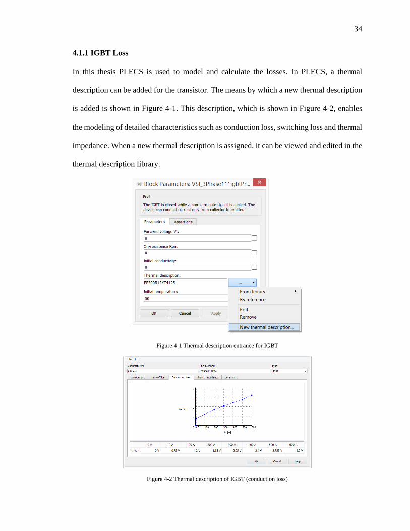
In this thesis PLECS is used to model and calculate the losses. In PLECS, a thermal
description can be added for the transistor. The means by which a new thermal description
is added is shown in Figure 4-1. This description, which is shown in Figure 4-2, enables
the modeling of detailed characteristics such as conduction loss, switching loss and thermal
impedance. When a new thermal description is assigned, it can be viewed and edited in the
thermal description library.
Figure 4-1 Thermal description entrance for IGBT
Figure 4-2 Thermal description of IGBT (conduction loss)
35
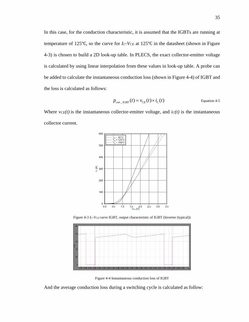
In this case, for the conduction characteristic, it is assumed that the IGBTs are running at
temperature of 125℃, so the curve for IC-VCE at 125℃ in the datasheet (shown in Figure
4-3) is chosen to build a 2D look-up table. In PLECS, the exact collector-emitter voltage
is calculated by using linear interpolation from these values in look-up table. A probe can
be added to calculate the instantaneous conduction loss (shown in Figure 4-4) of IGBT and
the loss is calculated as follows:
_ ( ) ( ) ( )con IGBT CE Cp t v t i t Equation 4-5
Where vCE(t) is the instantaneous collector-emitter voltage, and iC(t) is the instantaneous
collector current.
Figure 4-3 IC-VCE curve IGBT, output characteristic of IGBT (Inverter (typical))
Figure 4-4 Instantaneous conduction loss of IGBT
And the average conduction loss during a switching cycle is calculated as follow:
36
_
_
( )( )
st t
con IGBTt
con IGBT s
s
p t dtP t
t
Equation 4-6
Where ts is the switching period. A custom block in the PLECS model calculates the
average conduction loss.
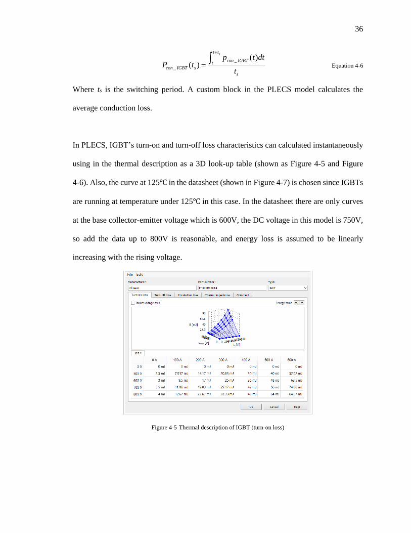
In PLECS, IGBT’s turn-on and turn-off loss characteristics can calculated instantaneously
using in the thermal description as a 3D look-up table (shown as Figure 4-5 and Figure
4-6). Also, the curve at 125℃ in the datasheet (shown in Figure 4-7) is chosen since IGBTs
are running at temperature under 125℃ in this case. In the datasheet there are only curves
at the base collector-emitter voltage which is 600V, the DC voltage in this model is 750V,
so add the data up to 800V is reasonable, and energy loss is assumed to be linearly
increasing with the rising voltage.
Figure 4-5 Thermal description of IGBT (turn-on loss)
37
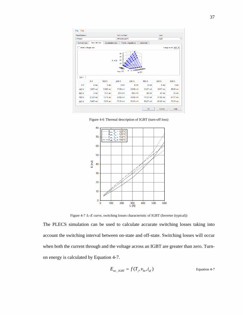
Figure 4-6 Thermal description of IGBT (turn-off loss)
Figure 4-7 IC-E curve, switching losses characteristic of IGBT (Inverter (typical))
The PLECS simulation can be used to calculate accurate switching losses taking into
account the switching interval between on-state and off-state. Switching losses will occur
when both the current through and the voltage across an IGBT are greater than zero. Turn-
on energy is calculated by Equation 4-7.
_ ( , , )on IGBT j be afE f T v i Equation 4-7

38
Where iaf is the current after switching, vbe is the voltage before switching and Tj is the
junction temperature.
While turn-off energy is calculated by Equation 4-8
_ ( , , )off IGBT j af beE f T v i Equation 4-8
Where ibe is the current before switching, vaf is the voltage after switching and Tj is the
junction temperature.
The total switching energy of the IGBT is calculated by Equation 4-9, Figure 4-8 shows
the result from PLECS.
_ _ _sw IGBT on IGBT off IGBTE E E Equation 4-9
Figure 4-8 Instantaneous switching loss of IGBT
The average switching loss during one switch period is calculated as follow:
_
_ ( )sw IGBT
sw IGBT s
s
EP t
t
Equation 4-10
Where ts is the switching period. A custom block in the PLECS model calculates the
average switching loss.
4.1.2 Diode Loss
This section describes the method by which the Si Diode losses are calculated.

39
As was the case for the IGBT, PLECS can be used to calculate the Diode conduction losses
by adding a thermal description for the diode, according to Figure 4-9. This description,
which is shown in Figure 4-10, enables the modeling of detailed characteristics such as
conduction loss, switching loss and thermal impedance. When a new thermal description
is assigned, it can be viewed and edited in the thermal description library.
Figure 4-9 Thermal description entrance of Diode
Figure 4-10 Thermal description of Diode (conduction loss)

40
In this case, for the conduction characteristic, diodes are running at temperature under
125℃, so the curve at 125℃ in the datasheet (shown in Figure 4-11) is chosen to build a
2D look-up table. In PLECS, the exact voltage is calculated by using linear interpolation
from these values in the look-up table. A probe can be added to calculate the instantaneous
conduction loss of the diode and the loss is calculated as follow:
_ ( ) ( ) ( )con diode on onp t v t i t Equation 4-11
Where von(t) is the instantaneous forward voltage, and ion(t) is the instantaneous forward
current. Figure 4-12 shows the result from PLECS.
Figure 4-11 IF-VF curve, forward characteristic of Diode (Inverter (typical))
Figure 4-12 Instantaneous conduction loss of Diode
And the average conduction loss during a switching cycle is calculated by:
41
_
_
( )( )
st t
con diodet
con diode s
s
p t dtP t
t
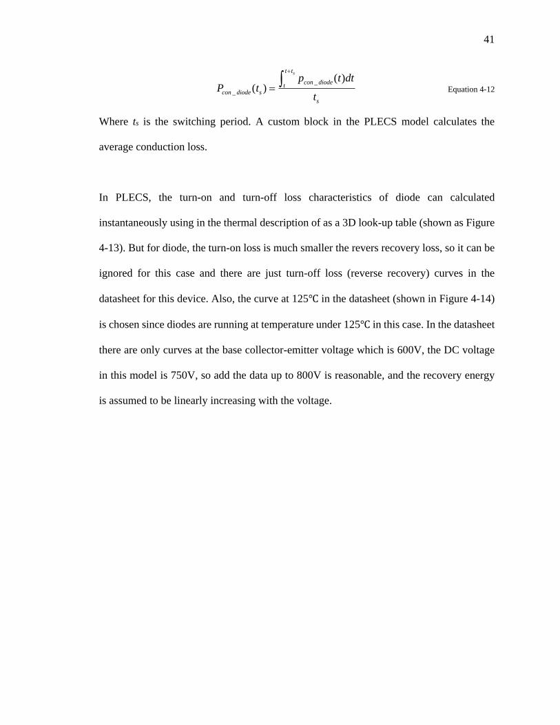
Equation 4-12
Where ts is the switching period. A custom block in the PLECS model calculates the
average conduction loss.
In PLECS, the turn-on and turn-off loss characteristics of diode can calculated
instantaneously using in the thermal description of as a 3D look-up table (shown as Figure
4-13). But for diode, the turn-on loss is much smaller the revers recovery loss, so it can be
ignored for this case and there are just turn-off loss (reverse recovery) curves in the
datasheet for this device. Also, the curve at 125℃ in the datasheet (shown in Figure 4-14)
is chosen since diodes are running at temperature under 125℃ in this case. In the datasheet
there are only curves at the base collector-emitter voltage which is 600V, the DC voltage
in this model is 750V, so add the data up to 800V is reasonable, and the recovery energy
is assumed to be linearly increasing with the voltage.

42
Figure 4-13 Thermal description of Diode (turn-off loss)
Figure 4-14 IF-E curve, switching losses characteristic of Diode (Inverter (typical))
In PLECS, the switching energy loss calculation is using the negative blocking voltage and
the turn-on loss is neglected, the turn-off loss can be calculated by Equation 4-13.
_ ( , , )off diode j af beE f T v i Equation 4-13

43
Where ibe is the current before switching, vaf is the voltage after switching and Tj is the
junction temperature. Figure 4-15 shows the result from PLECS.
Figure 4-15 Instantaneous switching loss of diode
And the average switching loss is calculated as follow:
_
_ ( )off diode
sw diode s
s
EP t
t
Equation 4-14
Where ts is the switching period. A custom block in the PLECS model calculates the
average switching loss.
4.2 Calculation for SiC MOSFET Losses
In SiC MOSFET module, there is no recovery current from diode. So for the diode there is
no switching loss. There is no turn-off tail current from MOSFET, this character decreases
the switching loss. The procedures to calculate SiC MOSFET losses in PLECS is similar
to those of Si IGBT, so do not repeat here. However, the curves in the SiC MOSFET
datasheet are at 25℃ or 150℃, so linearization should be made to get the counterpart at
125℃, but there is one exception for the switching loss curve, because of the switching
loss do not increase with temperature. Actually the total switching loss will go done a little
bit with the temperature goes up as shown in Figure 4-16.

44
Figure 4-16 Switching energy vs. temperature
4.3 Summary
For both Si IGBT and SiC MOSFET device, the conduction loss are independent of the
switching frequency, while switching loss will linearly increase with the switching
frequency goes up. Because of the advantage of SiC material, SiC MOSFET have a much
lower switching loss.
Chapter 5 Simulation Results and Analysis
5.1 Description of the Simulation Model
In this thesis, a simulation of a simple grid-forming inverter with open loop controls in
MATLAB/Simulink is built. It comes up with accurate representation of the pulsed
voltages that result from Third Harmonic Injection Pulse-Width Modulation (PWM)
controlled inverter and PLECS is used to simulate the losses in the inverter. The model
mainly consists of two parts: the control part and the inverter part as shown in Figure 5-1.

45
Figure 5-1 PV system model
For the control part shown in Figure 5-2, Third Harmonic Injection PWM control is applied
since the harmonics can be reduced and modulation depth can be improved according to
reference [33] with the minimum number of switch commutations, and this can ensure the
minimum filter size for a given switching frequency. It is a control strategy provides the
modulation index up to 1.15, which increases the DC voltage utilization and it is the same
to Space Vector PWM.
Figure 5-2 Control part of PV system
46
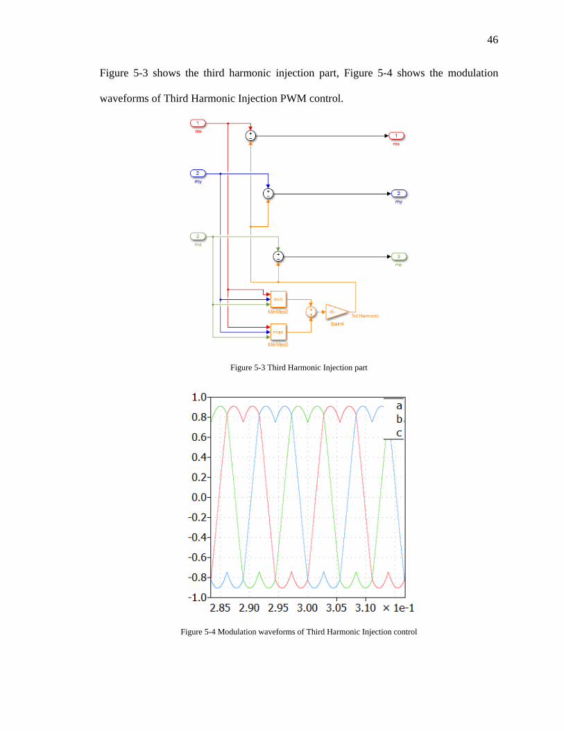
Figure 5-3 shows the third harmonic injection part, Figure 5-4 shows the modulation
waveforms of Third Harmonic Injection PWM control.
Figure 5-3 Third Harmonic Injection part
Figure 5-4 Modulation waveforms of Third Harmonic Injection control

47
And in this thesis naturally sampled PWM is used. The switching pattern can be seen in
Figure 5-8, it is symmetric and in every switching period only one switch device is changed,
which minimizes the switching loss.
Figure 5-5 Waveforms of phase-neutral voltage
PLECS Blockset is embedded in MATLAB/Simulink as a toolbox, which is used to build
the inverter in this thesis. The inverter part is shown in Figure 5-6, including the heatsink,
detailed semiconductor model and the loss calculation part.
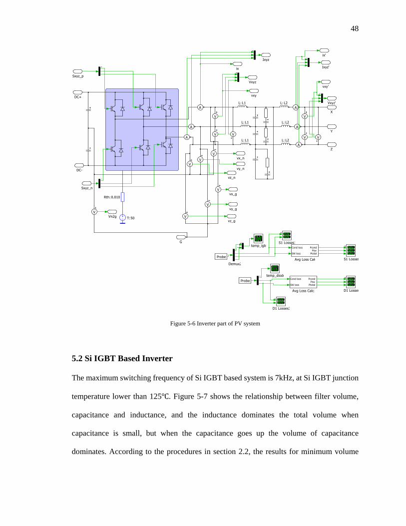
48
Figure 5-6 Inverter part of PV system
5.2 Si IGBT Based Inverter
The maximum switching frequency of Si IGBT based system is 7kHz, at Si IGBT junction
temperature lower than 125℃. Figure 5-7 shows the relationship between filter volume,
capacitance and inductance, and the inductance dominates the total volume when
capacitance is small, but when the capacitance goes up the volume of capacitance
dominates. According to the procedures in section 2.2, the results for minimum volume
49
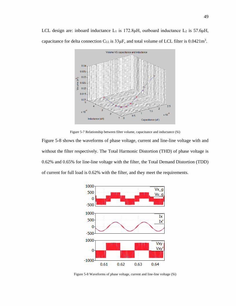
LCL design are: inboard inductance L1 is 172.8μH, outboard inductance L2 is 57.6μH,
capacitance for delta connection CLL is 33μF, and total volume of LCL filter is 0.0421m3.
Figure 5-7 Relationship between filter volume, capacitance and inductance (Si)
Figure 5-8 shows the waveforms of phase voltage, current and line-line voltage with and
without the filter respectively. The Total Harmonic Distortion (THD) of phase voltage is
0.62% and 0.65% for line-line voltage with the filter, the Total Demand Distortion (TDD)
of current for full load is 0.62% with the filter, and they meet the requirements.
Figure 5-8 Waveforms of phase voltage, current and line-line voltage (Si)

50
Figure 5-9 shows FFT analysis of phase voltage and current without LCL filter. It is clear
that the harmonics are around the switching frequency.
Figure 5-9 FFT analysis of phase voltage and current without LCL filter (Si)
Figure 5-10 shows FFT analysis of phase voltage and current with LCL filter. It is clear
that the harmonics around the switching frequency are attenuated.
Figure 5-10 FFT analysis of phase voltage and current with LCL filter (Si)
51
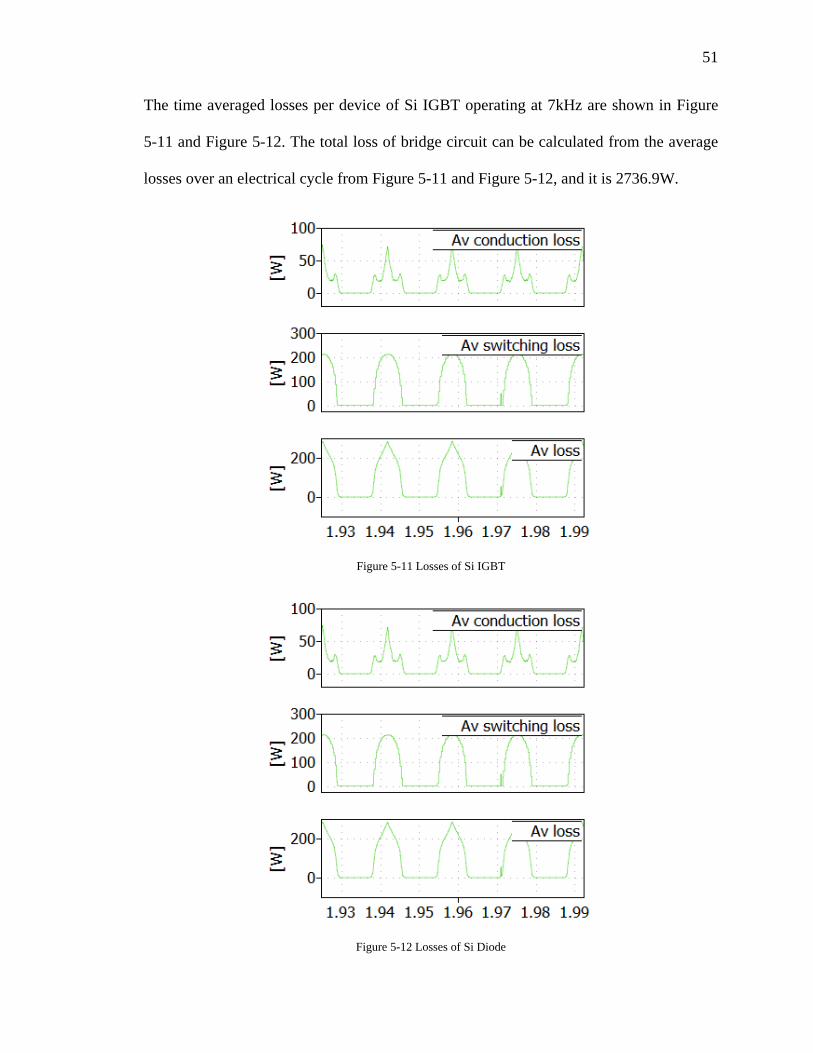
The time averaged losses per device of Si IGBT operating at 7kHz are shown in Figure
5-11 and Figure 5-12. The total loss of bridge circuit can be calculated from the average
losses over an electrical cycle from Figure 5-11 and Figure 5-12, and it is 2736.9W.
Figure 5-11 Losses of Si IGBT
Figure 5-12 Losses of Si Diode
52
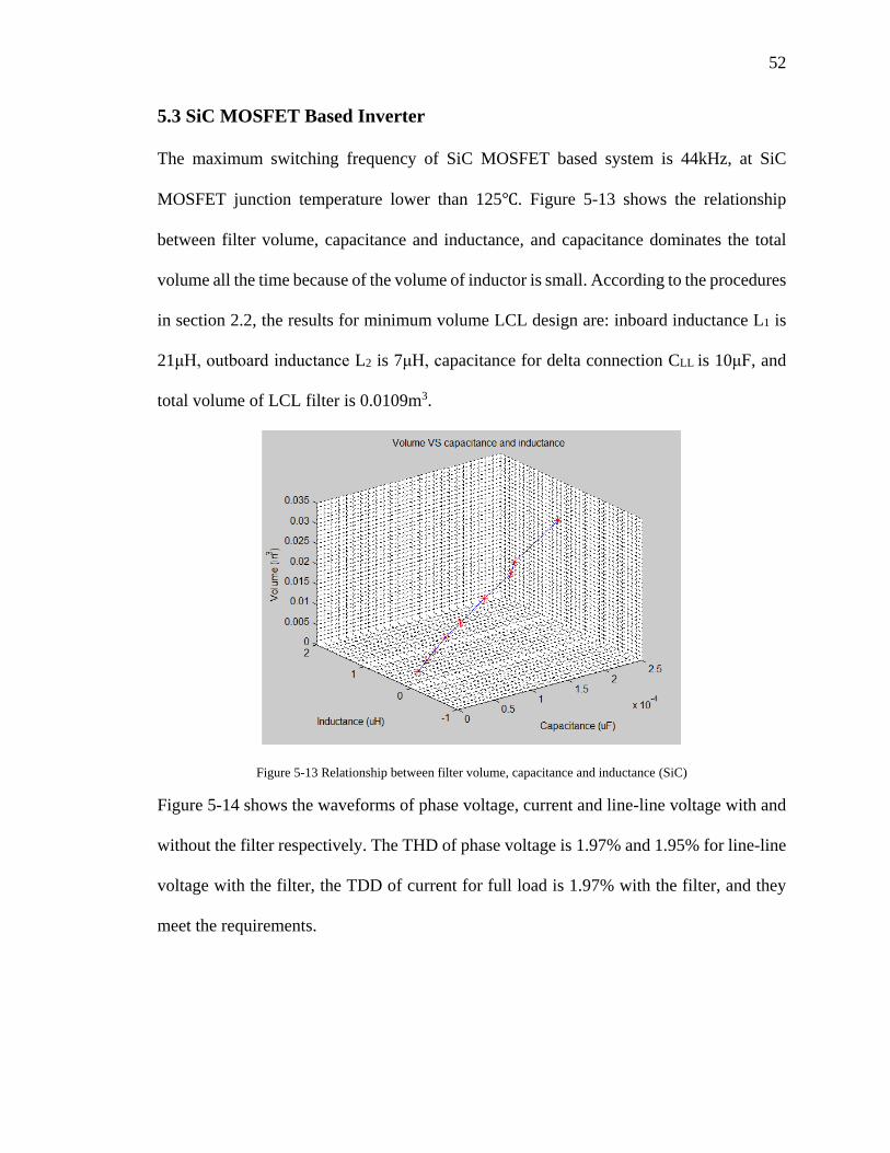
5.3 SiC MOSFET Based Inverter
The maximum switching frequency of SiC MOSFET based system is 44kHz, at SiC
MOSFET junction temperature lower than 125℃. Figure 5-13 shows the relationship
between filter volume, capacitance and inductance, and capacitance dominates the total
volume all the time because of the volume of inductor is small. According to the procedures
in section 2.2, the results for minimum volume LCL design are: inboard inductance L1 is
21μH, outboard inductance L2 is 7μH, capacitance for delta connection CLL is 10μF, and
total volume of LCL filter is 0.0109m3.
Figure 5-13 Relationship between filter volume, capacitance and inductance (SiC)
Figure 5-14 shows the waveforms of phase voltage, current and line-line voltage with and
without the filter respectively. The THD of phase voltage is 1.97% and 1.95% for line-line
voltage with the filter, the TDD of current for full load is 1.97% with the filter, and they
meet the requirements.

53
Figure 5-14 Waveforms of phase voltage, current and line-line voltage (SiC)
Figure 5-15 shows FFT analysis of phase voltage and current without LCL filter. It is clear
that the harmonics are around the switching frequency.
Figure 5-15 FFT analysis of phase voltage and current without LCL filter (SiC)
Figure 5-16 shows FFT analysis of phase voltage and current with LCL filter. It is clear
that the harmonics around the switching frequency are attenuated.

54
Figure 5-16 FFT analysis of phase voltage and current with LCL filter (SiC)
The losses per device of Si IGBT operating at 44kHz are shown in Figure 5-17 and Figure
5-18. The total loss of bridge circuit can be calculated from the average losses over an
electrical cycle from Figure 5-17 and Figure 5-18, and it is 2726.9W.
Figure 5-17 Losses of SiC MOSFET (44kHz)

55
Figure 5-18 Losses of SiC Diode (44kHz)
The losses per device of Si IGBT operating at 7kHz are shown in Figure 5-19 and Figure
5-20. The total loss of bridge circuit can be calculated from the average losses over an
electrical cycle from Figure 5-19 and Figure 5-20, and it is 1482.3W.
Figure 5-19 Losses of SiC MOSFET (7kHz)

56
Figure 5-20 Losses of SiC Diode (7kHz)
5.4 Comparison of Si Based Inverter and SiC Based Inverter
5.4.1 Power Density
It is necessary to get the total volume of the system to analysis the power density. First,
heatsink size for both systems in this thesis are the same since the Si IGBT module and
SiC MOSFET module are the same size, and it is assumed the maximum junction
temperature of the two modules are the same. Actually SiC MOSFET can operate at a
higher temperature, which could result in a smaller heatsink, but in this thesis, the main
objective to discuss the effect of replacing Si device with SiC device to the filter size.
In this system, capacitor LNU2H822MSEJ from Nichicon is chosen to build the DC link
capacitor with two capacitors in series and four parallel branches. From the datasheet, the
volume of DC link capacitor can be obtained and it is 0.0847m3.
57
According to section 3.2, assuming the height of bus bar which is on the top of the Si IGBT
(or SiC MOSFET) modules is 1 inch (25.4 mm). The volume of heatsink, Si IGBTs (or
SiC MOSFET) and the bus bar can be approximately obtained by Equation 5-1.
3 3150 532 (150 30.9 25.4) 16462740 0.0165sink chip busVolume mm m Equation 5-1
The total volume of the inverter based on Si IGBT can be obtained approximately by
Equation 5-2.
30.0847 0.0165 0.0421=0.1433InverterSiIGBTVolu mme Equation 5-2
The power density of the inverter based on Si IGBT can be obtained approximately by
Equation 5-3.
3 3=1395.7kW/ 0.0014 /Si
InverterSiIGBT
PowerRatingPowerdensity
Volum kW m
mec Equation 5-3
The total volume of the inverter based on SiC MOSFET can be obtained approximately by
Equation 5-4.
30.0847 0.0165 0.0109=0.1121InverterSiCMOSFETVolume m Equation 5-4
The power density of the inverter based on SiC MOSFET can be obtained approximately
by Equation 5-5.
3 3=1784.1kW/ 0.0018 /SiC
InverterSiCMOSFET
PowerRm
atingPowerdensity
VokW m
lumec Equation 5-5
SiC-based inverter has a greater power density (improved by 27.8%).
5.4.2 Energy Efficiency
The efficiency can be calculated by Equation 5-6.
100%rate loss
rate
P PEfficiency
P
Equation 5-6
58
For Si IGBT based inverter operating at 7kHz, the loss of the bridge circuit is 2736.9W,
the loss of filter is 220.1W, and the efficiency is 98.52%. For SiC MOSFET based inverter
operating at 7kHz, the loss of the bridge circuit is 1482.3W, the loss of filter is 220.1W, so
the efficiency is 99.15%. For SiC MOSFET based inverter operating at 44kHz, the loss of
the bridge circuit is 2726.9W, the loss of filter is 209.3W, so the efficiency is 98.53%.
It is clear that, SiC-based inverter is more efficient when comparing the two designs under
the constraint of keeping the junction temperature under 125℃. The efficiency for SiC-
based inverter decreased when switching frequency goes up from 7kHz to 44kHz, however,
SiC-based inverter operating at 44kHz is still a little bit more efficient than Si-based
inverter operating at 7kHz.
5.5 Summary
SiC based inverter is both more power dense and more efficient when comparing the two
designs. This conclusion was arrived at with a single constraint keeping the junction
temperature the same and using the same heatsink design. When operating at the same
switching frequency, which means keeping power density the same, SiC devices leads a
improvement in efficiency.

59
Chapter 6 Conclusion and Future Work
6.1 Conclusion
A methodology for making a valid comparison between SiC and Silicon designs for a Solar
Inverter is presented in this thesis. This same methodology can be applied to other
applications and will be useful going forward as the merits of SiC-based designs are further
proven.
The methodology demonstrated in this thesis comes up with a truly minimal filter size by
balancing the inductive and capacitive components to achieve the smallest total volume.
And as a result, SiC based inverter is both more power dense and more efficient when
comparing the two designs under the constraint of keeping the junction temperature the
same and using the same heatsink design. When operating at the same switching frequency,
which means keeping the power density the same, SiC devices leads an improvement in
efficiency.
6.2 Future Work
An even more power dense design by allowing SiC junction temperature to go to a higher
value, such 150℃. This approach would be perfectly acceptable because these devices can
operate at temperatures as high as 200℃ without failure. It would be accomplished by both
designing a smaller heatsink and operating at a higher switching frequency.

60
References
[1] IEA-PVPS, P. V. P. S. (2015). Report Snapshot of Global PV 1992-2014.Report IEA-
PVPS T1-26.
[2] Pinner, D., & Rogers, M. (2015). Solar Power Comes of Age. Foreign Affairs,94(2),
111-118.
[3] Hudgins, J. L., Simin, G. S., Santi, E., & Khan, M. A. (2003). An assessment of wide
bandgap semiconductors for power devices. Power Electronics, IEEE Transactions
on, 18(3), 907-914.
[4] Neudeck, P. G., Okojie, R. S., & Chen, L. Y. (2002). High-temperature electronics-a
role for wide bandgap semiconductors?. Proceedings of the IEEE,90(6), 1065-1076.
[5] ZHANG, B., DENG, X. C., CHEN, W. J., & LI, Z. J. (2009). Wide Bandgap
Semiconductors for Power Electronics [J]. Journal of University of Electronic Science
and Technology of China, 5, 019.
[6] Kaminski, N., & Hilt, O. (2014). SiC and GaN devices-wide bandgap is not all the
same. Circuits, Devices & Systems, IET, 8(3), 227-236.
[7] Liserre, M., Blaabjerg, F., & Hansen, S. (2005). Design and control of an LCL-filter-
based three-phase active rectifier. Industry Applications, IEEE Transactions on, 41(5),
1281-1291.
[8] Karshenas, H. R., & Saghafi, H. (2006, July). Basic criteria in designing LCL filters
for grid connected converters. In Industrial Electronics, 2006 IEEE International
Symposium on (Vol. 3, pp. 1996-2000). IEEE.
[9] Reznik, A., Simoes, M. G., Al-Durra, A., & Muyeen, S. M. (2014). Filter Design and
Performance Analysis for Grid-Interconnected Systems. Industry Applications, IEEE
Transactions on, 50(2), 1225-1232.
[10] Araujo, S.V., Engler, A., Sahan, B., & Antunes, F. L. M. (2007). LCL filter design for
grid-connected NPC inverters in offshore wind turbines. Power Electronics
Conference, 2007. ICPE '07. 7th Internatonal on , 1133-1138.
[11] Renzhong, X., Lie, X., Junjun, Z., & Jie, D. (2013). Design and research on the LCL
filter in three-phase PV grid-connected inverters. International Journal of Computer
and Electrical Engineering, 5(3), 322-325.
[12] Cho, J. H., Kim, D. H., Vircikova, M., & Sincak, P. (2011). Design of LCL filter using
hybrid intelligent optimization for photovoltaic system. In Ubiquitous Computing and
Multimedia Applications (pp. 90-97). Springer Berlin Heidelberg.

61
[13] Jeong, H. G., Yoon, D. K., & Lee, K. B. (2013). Design of an LCL-Filter for Three-
Parallel Operation of Power Converters in Wind Turbines. Journal of Power
Electronics, 13(3), 437-446.
[14] Koutroulis, E., & Blaabjerg, F. (2012). Methodology for the optimal design of
transformerless grid-connected PV inverters. Power Electronics, IET, 5(8), 1491-1499.
[15] Reznik, A., Simoes, M. G., Al-Durra, A., & Muyeen, S. M. (2012, July). LCL filter
design and performance analysis for small wind turbine systems. In Power Electronics
and Machines in Wind Applications (PEMWA), 2012 IEEE (pp. 1-7). IEEE.
[16] Wei, X., Xiao, L., Yao, Z., & Gong, C. (2010, November). Design of LCL filter for
wind power inverter. In World Non-Grid-Connected Wind Power and Energy
Conference (WNWEC), 2010 (pp. 1-6). IEEE.
[17] Cai,L., Chang, Z., Zhou, R.,& Song, X. (2011). Research on Grid-Connected Inverter
for 500 kW Photovoltaic Power System. In Advances of Power System & Hydroelectric
Engineering 27(12), 95-99.
[18] Liu, F., Zha, X., Zhou, Y., & Duan, S. (2009, May). Design and research on parameter
of LCL filter in three-phase grid-connected inverter. In Power Electronics and Motion
Control Conference, 2009. IPEMC'09. IEEE 6th International (pp. 2174-2177). IEEE.
[19] De, D., Castellazzi, A., Solomon, A., Trentin, A., Minami, M., & Hikihara, T. (2013,
September). An all SiC MOSFET high performance PV converter cell. In Power
Electronics and Applications (EPE), 2013 15th European Conference on (pp. 1-10).
IEEE.
[20] Sintamarean, C., Eni, E., Blaabjerg, F., Teodorescu, R., & Wang, H. (2014, May).
Wide-band gap devices in PV systems-opportunities and challenges. In Power
Electronics Conference (IPEC-Hiroshima 2014-ECCE-ASIA), 2014 International (pp.
1912-1919). IEEE.
[21] Sintamarean, C., Blaabjerg, F., Wang, H., & Yang, Y. (2013, September). Real field
mission profile oriented design of a SiC-based PV-inverter application. In Energy
Conversion Congress and Exposition (ECCE), 2013 IEEE (pp. 940-947). IEEE.
[22] Hazra, S., De, A., Cheng, L., Palmour, J., Schupbach, M., Hull, B., ... & Bhattacharya,
S. High Switching Performance of 1700V, 50A SiC Power MOSFET over Si
IGBT/BiMOSFET for Advanced Power Conversion Applications.
[23] Ho, C. N. M., Breuninger, H., Pettersson, S., Escobar, G., & Canales, F. (2013). A
comparative performance study of an interleaved boost converter using commercial Si
and SiC diodes for PV applications. Power Electronics, IEEE Transactions on, 28(1),
289-299.
[24] Sintamarean, C., Blaabjerg, F., & Wang, H. (2013, November). Comprehensive
evaluation on efficiency and thermal loading of associated Si and SiC based PV inverter
62
applications. In Industrial Electronics Society, IECON 2013-39th Annual Conference
of the IEEE (pp. 555-560). IEEE.
[25] Burkart, R. M., & Kolar, J. W. (2013, June). Comparative evaluation of SiC and Si PV
inverter systems based on power density and efficiency as indicators of initial cost and
operating revenue. In Control and Modeling for Power Electronics (COMPEL), 2013
IEEE 14th Workshop on (pp. 1-6). IEEE.
[26] Oswald, N., Anthony, P., McNeill, N., & Stark, B. H. (2014). An experimental
investigation of the tradeoff between switching losses and EMI generation with hard-
switched all-Si, Si-SiC, and all-SiC device combinations. Power Electronics, IEEE
Transactions on, 29(5), 2393-2407.
[27] Rodriguez, L., Williams, E., Balda, J. C., & Stewart, C. (2013, July). A comparison of
selected silicon and silicon-carbide switching devices for PV microinverter
applications. In Power Electronics for Distributed Generation Systems (PEDG), 2013
4th IEEE International Symposium on (pp. 1-7). IEEE.
[28] Zhao, T., Wang, J., Huang, A. Q., & Agarwal, A. (2007, September). Comparisons of
SiC MOSFET and Si IGBT based motor drive systems. In Industry Applications
Conference, 2007. 42nd IAS Annual Meeting. Conference Record of the 2007 IEEE (pp.
331-335). IEEE.
[29] Erickson, R. W. (1997). Filter Inductor Design. In Fundamentals of Power
Electronics (pp. 497-511). Springer US.
[30] Lee, S. (1995, February). Optimum design and selection of heatsinks.
In Semiconductor Thermal Measurement and Management Symposium, 1995. SEMI-
THERM XI., Eleventh Annual IEEE (pp. 48-54). IEEE.
[31] Lee, S. (1995). How to select a heatsink. electronics cooling, 1(1), 10-14.
[32] Seshasayee, N. (2011). Understanding Thermal Dissipation and Design of a
Heatsink. Texas Instruments, Dallas.
[33] Holmes, D. G. (1998, October). A general analytical method for determining the
theoretical harmonic components of carrier based PWM strategies. In Industry
Applications Conference, 1998. Thirty-Third IAS Annual Meeting. The 1998
IEEE (Vol. 2, pp. 1207-1214). IEEE.