ddr3 sdram sodimm fast data transfer rates: pc3...
TRANSCRIPT
DDR3 SDRAM SODIMMMT8JSF12864HZ – 1GBMT8JSF25664HZ – 2GB
Features• DDR3 functionality and operations supported as
defined in the component data sheet
• 204-pin, small-outline dual in-line memory module(SODIMM)
• Fast data transfer rates: PC3-12800, PC3-10600,PC3-8500, or PC3-6400
• 1GB (128 Meg x 64)
• 2GB (256 Meg x 64)
• VDD = 1.5V ±0.075V
• VDDSPD = +3.0V to +3.6V
• Nominal and dynamic on-die termination (ODT) fordata, strobe, and mask signals
• Single rank
• On-board I2C temperature sensor with integratedserial presence-detect (SPD) EEPROM
• 8 internal device banks
• Fixed burst chop (BC) of 4 and burst length (BL) of 8via the mode register set (MRS)
• Selectable BC4 or BL8 on-the-fly (OTF)
• Gold edge contacts
• Halogen-free
• Fly-by topology
• Terminated control, command, and address bus
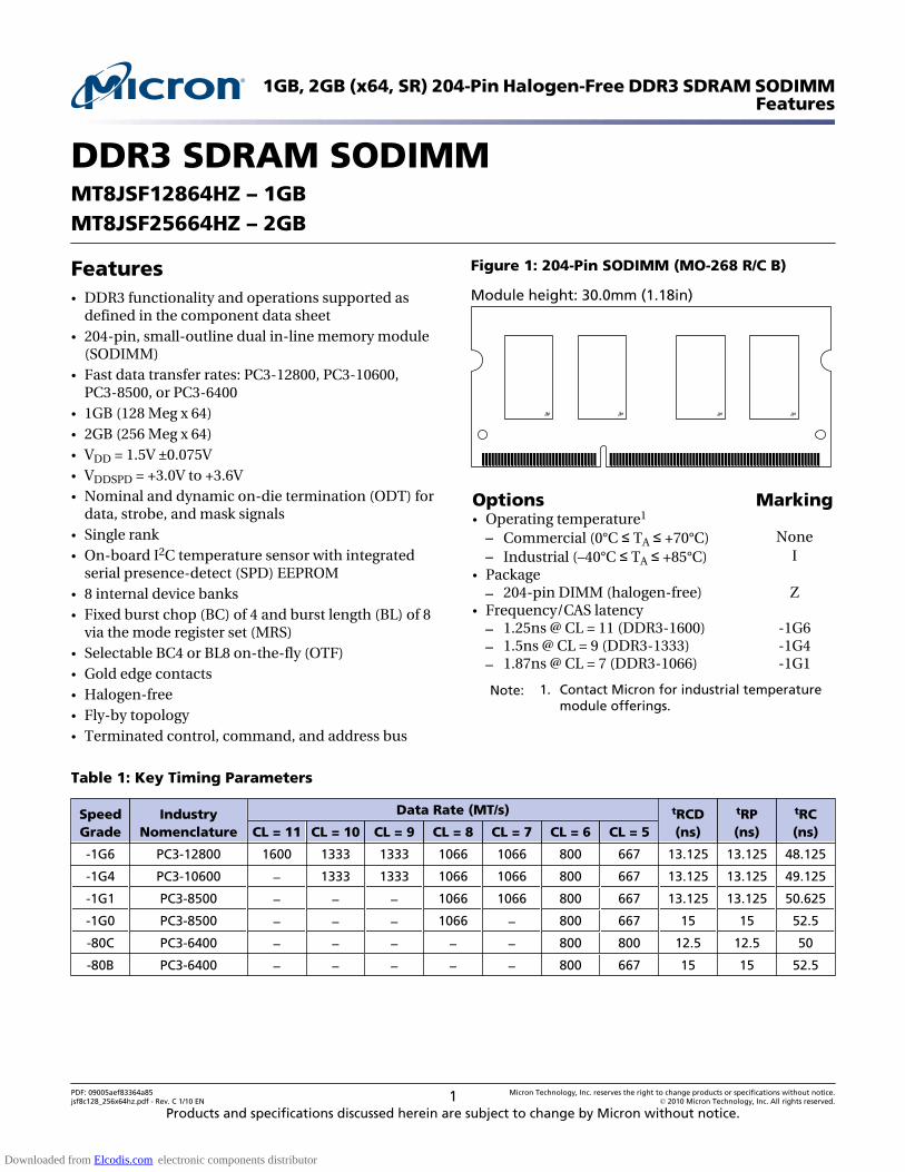
Figure 1: 204-Pin SODIMM (MO-268 R/C B)
Module height: 30.0mm (1.18in)
Options Marking• Operating temperature1
– Commercial (0°C ≤ TA ≤ +70°C) None– Industrial (–40°C ≤ TA ≤ +85°C) I
• Package – 204-pin DIMM (halogen-free) Z
• Frequency/CAS latency – 1.25ns @ CL = 11 (DDR3-1600) -1G6– 1.5ns @ CL = 9 (DDR3-1333) -1G4– 1.87ns @ CL = 7 (DDR3-1066) -1G1
Note: 1. Contact Micron for industrial temperaturemodule offerings.
Table 1: Key Timing Parameters
SpeedGrade
IndustryNomenclature
Data Rate (MT/s) tRCD(ns)
tRP(ns)
tRC(ns)CL = 11 CL = 10 CL = 9 CL = 8 CL = 7 CL = 6 CL = 5
-1G6 PC3-12800 1600 1333 1333 1066 1066 800 667 13.125 13.125 48.125
-1G4 PC3-10600 – 1333 1333 1066 1066 800 667 13.125 13.125 49.125
-1G1 PC3-8500 – – – 1066 1066 800 667 13.125 13.125 50.625
-1G0 PC3-8500 – – – 1066 – 800 667 15 15 52.5
-80C PC3-6400 – – – – – 800 800 12.5 12.5 50
-80B PC3-6400 – – – – – 800 667 15 15 52.5
1GB, 2GB (x64, SR) 204-Pin Halogen-Free DDR3 SDRAM SODIMMFeatures
PDF: 09005aef83364a85jsf8c128_256x64hz.pdf - Rev. C 1/10 EN 1 Micron Technology, Inc. reserves the right to change products or specifications without notice.
© 2010 Micron Technology, Inc. All rights reserved.
Products and specifications discussed herein are subject to change by Micron without notice.
Downloaded from Elcodis.com electronic components distributor

Table 2: Addressing
Parameter 1GB 2GB
Refresh count 8K 8K
Row address 16K A[13:0] 32K A[14:0]
Device bank address 8 BA[2:0] 8 BA[2:0]
Device configuration 1Gb (128 Meg x 8) 2Gb (256 Meg x 8)
Column address 1K A[9:0] 1K A[9:0]
Module rank address 1 S0# 1 S0#
Table 3: Part Numbers and Timing Parameters – 1GB Modules
Base device: MT41J128M8,1 1Gb DDR3 SDRAM
Part Number2ModuleDensity Configuration
ModuleBandwidth
Memory Clock/Data Rate
Clock Cycles(CL-tRCD-tRP)
MT8JSF12864H(I)Z-1G6__ 1GB 128 Meg x 64 12.8 GB/s 1.25ns/1600 MT/s 11-11-11
MT8JSF12864H(I)Z-1G4__ 1GB 128 Meg x 64 10.6 GB/s 1.5ns/1333 MT/s 9-9-9
MT8JSF12864H(I)Z-1G1__ 1GB 128 Meg x 64 8.5 GB/s 1.87ns/1066 MT/s 7-7-7
Table 4: Part Numbers and Timing Parameters – 2GB Modules
Base device: MT41J256M8,1 2Gb DDR3 SDRAM
Part Number22ModuleDensity Configuration
ModuleBandwidth
Memory Clock/Data Rate
Clock Cycles(CL-tRCD-tRP)
MT8JSF25664H(I)Z-1G6__ 2GB 256 Meg x 64 12.8 GB/s 1.25ns/1600 MT/s 11-11-11
MT8JSF25664H(I)Z-1G4__ 2GB 256 Meg x 64 10.6 GB/s 1.5ns/1333 MT/s 9-9-9
MT8JSF25664H(I)Z-1G1__ 2GB 256 Meg x 64 8.5 GB/s 1.87ns/1066 MT/s 7-7-7
Notes: 1. The data sheet for the base device can be found on Micron’s Web site.2. All part numbers end with a two-place code (not shown) that designates component and PCB revisions.
Consult factory for current revision codes. Example: MT8JSF12864HZ-1G1D1.
1GB, 2GB (x64, SR) 204-Pin Halogen-Free DDR3 SDRAM SODIMMFeatures
PDF: 09005aef83364a85jsf8c128_256x64hz.pdf - Rev. C 1/10 EN 2 Micron Technology, Inc. reserves the right to change products or specifications without notice.
© 2010 Micron Technology, Inc. All rights reserved.
Downloaded from Elcodis.com electronic components distributor
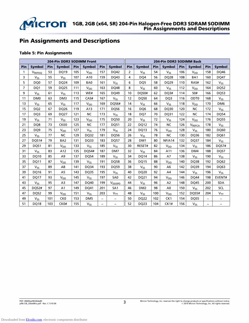
Pin Assignments and Descriptions
Table 5: Pin Assignments
204-Pin DDR3 SODIMM Front 204-Pin DDR3 SODIMM Back
Pin Symbol Pin Symbol Pin Symbol Pin Symbol Pin Symbol Pin Symbol Pin Symbol Pin Symbol
1 VREFDQ 53 DQ19 105 VDD 157 DQ42 2 VSS 54 VSS 106 VDD 158 DQ46
3 VSS 55 VSS 107 A10 159 DQ43 4 DQ4 56 DQ28 108 BA1 160 DQ47
5 DQ0 57 DQ24 109 BA0 161 VSS 6 DQ5 58 DQ29 110 RAS# 162 VSS
7 DQ1 59 DQ25 111 VDD 163 DQ48 8 VSS 60 VSS 112 VDD 164 DQ52
9 VSS 61 VSS 113 WE# 165 DQ49 10 DQS0# 62 DQ3# 114 S0# 166 DQ53
11 DM0 63 DM3 115 CAS# 167 VSS 12 DQS0 64 DQ3 116 ODT0 168 VSS
13 VSS 65 VSS 117 VDD 169 DQS6# 14 VSS 66 VSS 118 VDD 170 DM6
15 DQ2 67 DQ26 119 A13 171 DQS6 16 DQ6 68 DQ30 120 NC 172 VSS
17 DQ3 69 DQ27 121 NC 173 VSS 18 DQ7 70 DQ31 122 NC 174 DQ54
19 VSS 71 VSS 123 VDD 175 DQ50 20 VSS 72 VSS 124 VDD 176 DQ55
21 DQ8 73 CKE0 125 NC 177 DQ51 22 DQ12 74 NC 126 VREFCA 178 VSS
23 DQ9 75 VDD 127 VSS 179 VSS 24 DQ13 76 VDD 128 VSS 180 DQ60
25 VSS 77 NC 129 DQ32 181 DQ56 26 VSS 78 NC 130 DQ36 182 DQ61
27 DQS1# 79 BA2 131 DQ33 183 DQ57 28 DM1 80 NF/A14 132 DQ37 184 VSS
29 DQS1 81 VDD 133 VSS 185 VSS 30 RESET# 82 VDD 134 VSS 186 DQS7#
31 VSS 83 A12 135 DQS4# 187 DM7 32 VSS 84 A11 136 DM4 188 DQS7
33 DQ10 85 A9 137 DQS4 189 VSS 34 DQ14 86 A7 138 VSS 190 VSS
35 DQ11 87 VDD 139 VSS 191 DQ58 36 DQ15 88 VDD 140 DQ38 192 DQ62
37 VSS 89 A8 141 DQ34 193 DQ59 38 VSS 90 A6 142 DQ39 194 DQ63
39 DQ16 91 A5 143 DQ35 195 VSS 40 DQ20 92 A4 144 VSS 196 VSS
41 DQ17 93 VDD 145 VSS 197 SA0 42 DQ21 94 VDD 146 DQ44 198 EVENT#
43 VSS 95 A3 147 DQ40 199 VDDSPD 44 VSS 96 A2 148 DQ45 200 SDA
45 DQS2# 97 A1 149 DQ41 201 SA1 46 DM2 98 A0 150 VSS 202 SCL
47 DQS2 99 VDD 151 VSS 203 VTT 48 VSS 100 VDD 152 DQS5# 204 VTT
49 VSS 101 CK0 153 DM5 – – 50 DQ22 102 CK1 154 DQS5 – –51 DQ18 103 CK0# 155 VSS – – 52 DQ23 104 CK1# 156 VSS – –
1GB, 2GB (x64, SR) 204-Pin Halogen-Free DDR3 SDRAM SODIMMPin Assignments and Descriptions
PDF: 09005aef83364a85jsf8c128_256x64hz.pdf - Rev. C 1/10 EN 3 Micron Technology, Inc. reserves the right to change products or specifications without notice.
© 2010 Micron Technology, Inc. All rights reserved.
Downloaded from Elcodis.com electronic components distributor

Table 6: Pin Descriptions
Symbol Type Description
A[14:0] Input Address inputs: Provide the row address for ACTIVATE commands, and the column ad-dress and auto precharge bit (A10) for READ/WRITE commands, to select one location outof the memory array in the respective bank. A10 is sampled during a PRECHARGE com-mand to determine whether the PRECHARGE applies to one bank (A10 LOW, bank selec-ted by BA[2:0]) or all banks (A10 HIGH). If only one bank is to be precharged, the bank isselected by BA. A12 is also used for BC4/BL8 identification as “BL on-the-fly” during CAScommands. The address inputs also provide the op-code during the mode register com-mand set. A[13:0] address the 1Gb DDR3 devices. A[14:0] address the 2Gb DDR3 devices.
BA[2:0] Input Bank address inputs: BA[2:0] define the device bank to which an ACTIVATE, READ,WRITE, or PRECHARGE command is being applied. BA[2:0] define which mode register(MR0, MR1, MR2, and MR3) is loaded during the LOAD MODE command.
CK0, CK0# Input Clock: CK and CK# are differential clock inputs. All control, command, and address inputsignals are sampled on the crossing of the positive edge of CK and the negative edge of CK#.
CKE0 Input Clock enable: CKE enables (registered HIGH) and disables (registered LOW) internal circui-try and clocks on the DRAM.
DM[7:0] Input Input data mask: DM is an input mask signal for write data. Input data is masked whenDM is sampled HIGH, along with the input data, during a write access. DM is sampled onboth edges of the DQS. Although the DM pins are input-only, the DM loading is designedto match that of the DQ and DQS pins.
ODT0 Input On-die termination: ODT enables (registered HIGH) and disables (registered LOW) termi-nation resistance internal to the DRAM. When enabled in normal operation, ODT is onlyapplied to the following pins: DQ, DQS, DQS#, and DM. The ODT input will be ignored ifdisabled via the LOAD MODE command.
RAS#, CAS#,WE#
Input Command inputs: RAS#, CAS#, and WE# (along with S#) define the command being en-tered.
RESET# Input(LVCMOS)
Reset: RESET# is an active LOW CMOS input referenced to VSS. The RESET# input receiver isa CMOS input defined as a rail-to-rail signal with DC HIGH ≥ 0.8 × VDD and DC LOW ≤ 0.2 ×VDD. RESET# assertion and deassertion are asynchronous.
S0# Input Chip select: S# enables (registered LOW) and disables (registered HIGH) the command de-coder.
SA[1:0] Input Serial address inputs: These pins are used to configure the temperature sensor/SPD EE-PROM address range on the I2C bus.
SCL Input Serial clock for temperature sensor/SPD EEPROM: SCL is used to synchronize communi-cation to and from the temperature sensor/SPD EEPROM.
DQ[63:0] I/O Data input/output: Bidirectional data bus.
DQS[7:0],DQS#[7:0]
I/O Data strobe: DQS and DQS# are differential data strobes. Output with read data. Edge-aligned with read data. Input with write data. Center-aligned with write data.
SDA I/O Serial data: SDA is a bidirectional pin used to transfer addresses and data into and out ofthe temperature sensor/SPD EEPROM on the module on the I2C bus.
EVENT# Output(open drain)
Temperature event: The EVENT# pin is asserted by the temperature sensor when criticaltemperature thresholds have been exceeded.
VDD Supply Power supply: 1.5V ±0.075V. The component VDD and VDDQ are connected to the moduleVDD.
1GB, 2GB (x64, SR) 204-Pin Halogen-Free DDR3 SDRAM SODIMMPin Assignments and Descriptions
PDF: 09005aef83364a85jsf8c128_256x64hz.pdf - Rev. C 1/10 EN 4 Micron Technology, Inc. reserves the right to change products or specifications without notice.
© 2010 Micron Technology, Inc. All rights reserved.
Downloaded from Elcodis.com electronic components distributor
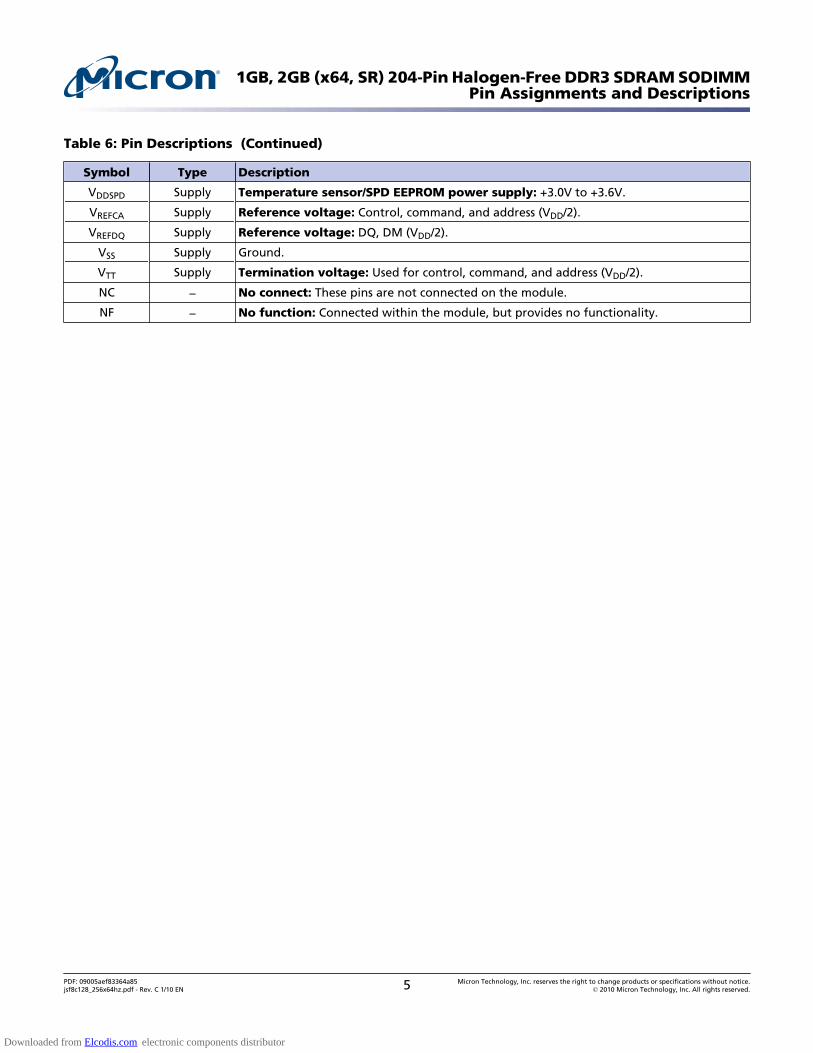
Table 6: Pin Descriptions (Continued)
Symbol Type Description
VDDSPD Supply Temperature sensor/SPD EEPROM power supply: +3.0V to +3.6V.
VREFCA Supply Reference voltage: Control, command, and address (VDD/2).
VREFDQ Supply Reference voltage: DQ, DM (VDD/2).
VSS Supply Ground.
VTT Supply Termination voltage: Used for control, command, and address (VDD/2).
NC – No connect: These pins are not connected on the module.
NF – No function: Connected within the module, but provides no functionality.
1GB, 2GB (x64, SR) 204-Pin Halogen-Free DDR3 SDRAM SODIMMPin Assignments and Descriptions
PDF: 09005aef83364a85jsf8c128_256x64hz.pdf - Rev. C 1/10 EN 5 Micron Technology, Inc. reserves the right to change products or specifications without notice.
© 2010 Micron Technology, Inc. All rights reserved.
Downloaded from Elcodis.com electronic components distributor
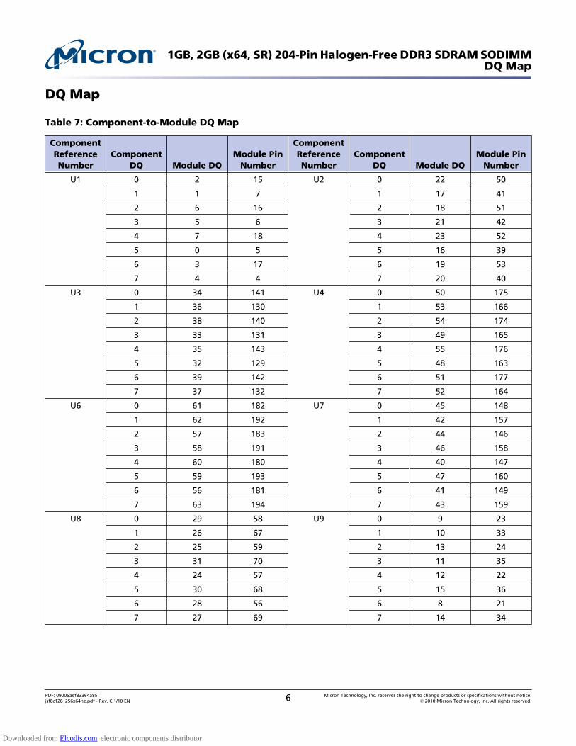
DQ Map
Table 7: Component-to-Module DQ Map
ComponentReferenceNumber
ComponentDQ Module DQ
Module PinNumber
ComponentReferenceNumber
ComponentDQ Module DQ
Module PinNumber
U1 0 2 15 U2 0 22 50
1 1 7 1 17 41
2 6 16 2 18 51
3 5 6 3 21 42
4 7 18 4 23 52
5 0 5 5 16 39
6 3 17 6 19 53
7 4 4 7 20 40
U3 0 34 141 U4 0 50 175
1 36 130 1 53 166
2 38 140 2 54 174
3 33 131 3 49 165
4 35 143 4 55 176
5 32 129 5 48 163
6 39 142 6 51 177
7 37 132 7 52 164
U6 0 61 182 U7 0 45 148
1 62 192 1 42 157
2 57 183 2 44 146
3 58 191 3 46 158
4 60 180 4 40 147
5 59 193 5 47 160
6 56 181 6 41 149
7 63 194 7 43 159
U8 0 29 58 U9 0 9 23
1 26 67 1 10 33
2 25 59 2 13 24
3 31 70 3 11 35
4 24 57 4 12 22
5 30 68 5 15 36
6 28 56 6 8 21
7 27 69 7 14 34
1GB, 2GB (x64, SR) 204-Pin Halogen-Free DDR3 SDRAM SODIMMDQ Map
PDF: 09005aef83364a85jsf8c128_256x64hz.pdf - Rev. C 1/10 EN 6 Micron Technology, Inc. reserves the right to change products or specifications without notice.
© 2010 Micron Technology, Inc. All rights reserved.
Downloaded from Elcodis.com electronic components distributor

Functional Block Diagram
Figure 2: Functional Block Diagram
DQ DQ DQ DQ DQ DQ DQ DQZQ
DQ0 DQ1 DQ2 DQ3 DQ4 DQ5 DQ6 DQ7
U1
DM CS# DQS DQS# DQ DQ DQ DQ DQ DQ DQ DQZQ
DQ32 DQ33 DQ34 DQ35 DQ36 DQ37 DQ38 DQ39
U3
DM CS# DQS DQS#
DQ DQ DQ DQ DQ DQ DQ DQZQ
DQ8 DQ9 DQ10 DQ11 DQ12 DQ13 DQ14 DQ15
U9
DM CS# DQS DQS#
DQ DQ DQ DQ DQ DQ DQ DQZQ
DQ16 DQ17 DQ18 DQ19 DQ20 DQ21 DQ22 DQ23
U2
DM CS# DQS DQS#
DQ DQ DQ DQ DQ DQ DQ DQZQ
DQ24 DQ25 DQ26 DQ27 DQ28 DQ29 DQ30 DQ31
U8
DM CS# DQS DQS#
DQ DQ DQ DQ DQ DQ DQ DQZQ
DQ40 DQ41 DQ42 DQ43 DQ44 DQ45 DQ46 DQ47
U7
DM CS# DQS DQS#
DQ DQ DQ DQ DQ DQ DQ DQZQ
DQ48 DQ49 DQ50 DQ51 DQ52 DQ53 DQ54 DQ55
U4
DM CS# DQS DQS#
DQ DQ DQ DQ DQ DQ DQ DQZQ
DQ56 DQ57 DQ58 DQ59 DQ60 DQ61 DQ62 DQ63
U6
DM CS# DQS DQS#
DQS0# DQS0 DM0
S0#
DQS1# DQS1 DM1
DQS2# DQS2 DM2
DQS3# DQS3 DM3
DQS4# DQS4 DM4
DQS5# DQS5 DM5
DQS6# DQS6 DM6
DQS7# DQS7 DM7
BA[2:0] A[14/13:0]
RAS#CAS# WE#
CKE0 ODT0
RESET#
BA[2:0]: DDR3 SDRAM A[14/13:0]: DDR3 SDRAM RAS#: DDR3 SDRAM CAS#: DDR3 SDRAM WE#: DDR3 SDRAM CKE0: DDR3 SDRAM ODT0: DDR3 SDRAM RESET#: DDR3 SDRAM
DDR3 SDRAM x 8CK0
CK0#
CK1CK1#
VREFCA
VSS
DDR3 SDRAM
DDR3 SDRAM
VDD
DDR3 SDRAM
VDDSPD Temperature sensor/SPD EEPROM
VTT
DDR3 SDRAM
DDR3 SDRAMVREFDQ
Clock, control, command, and address line terminations:
VSS
A0
Temperature sensor/
SPD EEPROMA1 A2
SA0 SA1
SDASCL
EVT
EVENT#
U10
VSS
VSS
VSSVSS
VSS
VSS
VSS
CKE0, A[14/13:0], RAS#, CAS#, WE#,
S0#, ODT0, BA[2:0]
DDR3 SDRAM
VTT
CK CK#
DDR3 SDRAM
VDD
VSS
Note: 1. The ZQ ball on each DDR3 component is connected to an external 240Ω ±1% resistorthat is tied to ground. It is used for the calibration of the component’s ODT and outputdriver.
1GB, 2GB (x64, SR) 204-Pin Halogen-Free DDR3 SDRAM SODIMMFunctional Block Diagram
PDF: 09005aef83364a85jsf8c128_256x64hz.pdf - Rev. C 1/10 EN 7 Micron Technology, Inc. reserves the right to change products or specifications without notice.
© 2010 Micron Technology, Inc. All rights reserved.
Downloaded from Elcodis.com electronic components distributor
General DescriptionDDR3 SDRAM modules are high-speed, CMOS dynamic random access memory mod-ules that use internally configured 8-bank DDR3 SDRAM devices. DDR3 SDRAM mod-ules use DDR architecture to achieve high-speed operation. DDR3 architecture isessentially an 8n-prefetch architecture with an interface designed to transfer two datawords per clock cycle at the I/O pins. A single read or write access for the DDR3 SDRAMmodule effectively consists of a single 8n-bit-wide, one-clock-cycle data transfer at theinternal DRAM core and eight corresponding n-bit-wide, one-half-clock-cycle data trans-fers at the I/O pins.
DDR3 modules use two sets of differential signals: DQS, DQS# to capture data and CKand CK# to capture commands, addresses, and control signals. Differential clocks anddata strobes ensure exceptional noise immunity for these signals and provide precisecrossing points to capture input signals.
Fly-By TopologyDDR3 modules use faster clock speeds than earlier DDR technologies, making signalquality more important than ever. For improved signal quality, the clock, control, com-mand, and address buses have been routed in a fly-by topology, where each clock,control, command, and address pin on each DRAM is connected to a single trace andterminated (rather than a tree structure, where the termination is off the module nearthe connector). Inherent to fly-by topology, the timing skew between the clock and DQSsignals can be easily accounted for by using the write-leveling feature of DDR3.
1GB, 2GB (x64, SR) 204-Pin Halogen-Free DDR3 SDRAM SODIMMGeneral Description
PDF: 09005aef83364a85jsf8c128_256x64hz.pdf - Rev. C 1/10 EN 8 Micron Technology, Inc. reserves the right to change products or specifications without notice.
© 2010 Micron Technology, Inc. All rights reserved.
Downloaded from Elcodis.com electronic components distributor
Electrical SpecificationsStresses greater than those listed may cause permanent damage to the module. This is astress rating only, and functional operation of the module at these or any other condi-tions outside those indicated in each device’s data sheet is not implied. Exposure toabsolute maximum rating conditions for extended periods may adversely affect reliability.
Table 8: Absolute Maximum Ratings
Symbol Parameter Min Max Units
VDD VDD supply voltage relative to VSS –0.4 +1.975 V
VIN, VOUT Voltage on any pin relative to VSS –0.4 +1.975 V
Table 9: Operating Conditions
Symbol Parameter Min Nom Max Units Notes
VDD VDD supply voltage 1.425 1.5 1.575 V
IVTT Termination reference current from VTT –600 – +600 mA
VTT Termination reference voltage (DC) –command/address bus
0.49 × VDD - 20mV 0.5 × VDD 0.51 × VDD + 20mV V 1
II Input leakage current;Any input 0V ≤ VIN ≤VDD;VREF input 0V ≤ VIN ≤0.95V (All other pinsnot under test = 0V)
Address in-puts, RAS#,CAS#, WE#,S#, CKE, ODT,BA, CK, CK#
–16 0 +16 µA
DM –2 0 +2
IOZ Output leakage current;0V ≤ VOUT ≤ VDD;DQ and ODT aredisabled; ODT is HIGH
DQ, DQS,DQS#
–5 0 +5 µA
IVREF VREF supply leakage current;VREFDQ = VDD/2 or VREFCA = VDD/2(All other pins not under test = 0V)
–8 0 +8 µA
TA Module ambientoperating temperature
Commercial 0 – +70 °C 2, 3
Industrial –40 – +85 °C
TC DDR3 SDRAM compo-nent case operatingtemperature
Commercial 0 – +95 °C 2, 3, 4
Industrial –40 – +95 °C
Notes: 1. VTT termination voltage in excess of the stated limit will adversely affect the commandand address signals’ voltage margin and will reduce timing margins.
2. TA and TC are simultaneous requirements.3. For further information, refer to technical note TN-00-08: “Thermal Applications,”
available on Micron’s Web site.4. The refresh rate is required to double when 85°C < TC ≤ 95°C.
1GB, 2GB (x64, SR) 204-Pin Halogen-Free DDR3 SDRAM SODIMMElectrical Specifications
PDF: 09005aef83364a85jsf8c128_256x64hz.pdf - Rev. C 1/10 EN 9 Micron Technology, Inc. reserves the right to change products or specifications without notice.
© 2010 Micron Technology, Inc. All rights reserved.
Downloaded from Elcodis.com electronic components distributor
DRAM Operating ConditionsRecommended AC operating conditions are given in the DDR3 component data sheets.Component specifications are available on Micron’s Web site. Module speed grades cor-relate with component speed grades, as shown below.
Table 10: Module and Component Speed Grades
DDR3 components may exceed the listed module speed grades; module may not be available in all listed speed grades
Module Speed Grade Component Speed Grade
-1G6 -125
-1G4 -15E
-1G1 -187E
-1G0 -187
-80C -25E
-80B -25
Design Considerations
Simulations
Micron memory modules are designed to optimize signal integrity through carefully de-signed terminations, controlled board impedances, routing topologies, trace lengthmatching, and decoupling. However, good signal integrity starts at the system level. Mi-cron encourages designers to simulate the signal characteristics of the system’s memo-ry bus to ensure adequate signal integrity of the entire memory system.
Power
Operating voltages are specified at the DRAM, not at the edge connector of the module.Designers must account for any system voltage drops at anticipated power levels to en-sure the required supply voltage is maintained.
1GB, 2GB (x64, SR) 204-Pin Halogen-Free DDR3 SDRAM SODIMMElectrical Specifications
PDF: 09005aef83364a85jsf8c128_256x64hz.pdf - Rev. C 1/10 EN 10 Micron Technology, Inc. reserves the right to change products or specifications without notice.
© 2010 Micron Technology, Inc. All rights reserved.
Downloaded from Elcodis.com electronic components distributor

IDD Specifications
Table 11: DDR3 IDD Specifications and Conditions – 1GB
Values are for the MT41J128M8 DDR3 SDRAM only and are computed from values specified in the 1Gb (128 Meg x 8)component data sheet
Parameter Symbol 1600 1333 1066 Units
Operating current 0: One bank ACTIVATE-to-PRE-CHARGE
IDD0 960 880 800 mA
Operating current 1: One bank ACTIVATE-to-READ-to-PRECHARGE
IDD1 1120 1040 960 mA
Precharge power-down current: Slow exit IDD2P 96 96 96 mA
Precharge power-down current: Fast exit IDD2P 360 320 280 mA
Precharge quiet standby current IDD2Q 536 480 424 mA
Precharge standby current IDD2N 560 520 440 mA
Precharge standby ODT current IDD2NT 760 680 600 mA
Active power-down current IDD3P 360 320 280 mA
Active standby current IDD3N 536 496 456 mA
Burst read operating current IDD4R 2000 1600 1280 mA
Burst write operating current IDD4W 2000 1760 1520 mA
Refresh current IDD5 2080 1920 1760 mA
Self refresh temperature current: MAX TC = 85°C IDD6 48 48 48 mA
Self refresh temperature current (SRT-enabled): MAXTC = 95°C
IDD6ET 72 72 72 mA
All banks interleaved read current IDD7 4800 3920 3120 mA
Reset current IDD8 112 112 112 mA
1GB, 2GB (x64, SR) 204-Pin Halogen-Free DDR3 SDRAM SODIMMElectrical Specifications
PDF: 09005aef83364a85jsf8c128_256x64hz.pdf - Rev. C 1/10 EN 11 Micron Technology, Inc. reserves the right to change products or specifications without notice.
© 2010 Micron Technology, Inc. All rights reserved.
Downloaded from Elcodis.com electronic components distributor

Table 12: DDR3 IDD Specifications and Conditions – 2GB
Values are for the MT41J256M8 DDR3 SDRAM only and are computed from values specified in the 2Gb (256 Meg x 8)component data sheet
Parameter Symbol 1600 1333 1066 Units
Operating current 0: One bank ACTIVATE-to-PRE-CHARGE
IDD0 TBD 720 640 mA
Operating current 1: One bank ACTIVATE-to-READ-to-PRECHARGE
IDD1 TBD 920 800 mA
Precharge power-down current: Slow exit IDD2P TBD 96 96 mA
Precharge power-down current: Fast exit IDD2P TBD 280 240 mA
Precharge quiet standby current IDD2Q TBD 520 440 mA
Precharge standby current IDD2N TBD 520 440 mA
Precharge standby ODT current IDD2NT TBD 680 600 mA
Active power-down current IDD3P TBD 360 320 mA
Active standby current IDD3N TBD 600 480 mA
Burst read operating current IDD4R TBD 1600 1280 mA
Burst write operating current IDD4W TBD 1920 1600 mA
Refresh current IDD5 TBD 2040 1960 mA
Self refresh temperature current: MAX TC = 85°C IDD6 TBD 72 72 mA
Self refresh temperature current (SRT-enabled): MAXTC = 95°C
IDD6ET TBD 96 96 mA
All banks interleaved read current IDD7 TBD 2920 2560 mA
Reset current IDD8 TBD 112 112 mA
1GB, 2GB (x64, SR) 204-Pin Halogen-Free DDR3 SDRAM SODIMMElectrical Specifications
PDF: 09005aef83364a85jsf8c128_256x64hz.pdf - Rev. C 1/10 EN 12 Micron Technology, Inc. reserves the right to change products or specifications without notice.
© 2010 Micron Technology, Inc. All rights reserved.
Downloaded from Elcodis.com electronic components distributor
Temperature Sensor with Serial Presence-Detect EEPROMThe temperature from the integrated thermal sensor is monitored and converts into adigital word via the I2C bus. System designers can use the user-programmable registersto create a custom temperature-sensing solution based on system requirements. Pro-gramming and configuration details comply with JEDEC standard No. 21-C page 4.7-1,“Definition of the TSE2002av, Serial Presence Detect with Temperature Sensor.”
Serial Presence-Detect EEPROM OperationDDR3 SDRAM modules incorporate serial presence-detect. The SPD data is stored in a256-byte EEPROM. The first 128 bytes are programmed by Micron to comply with JE-DEC standard JC-45, “Appendix X: Serial Presence Detect (SPD) for DDR3 SDRAMModules.” These bytes identify module-specific timing parameters, configuration infor-mation, and physical attributes. User-specific information can be written into theremaining 128 bytes of storage. READ/WRITE operations between the system (master)and the EEPROM (slave) device occur via an I2C bus. Write protect (WP) is connected toVSS, permanently disabling hardware write protect. For further information please referto Micron technical note TN-04-42, "Memory Module Serial Presence-Detect."
Table 13: Temperature Sensor with Serial Presence-Detect EEPROM Operating Conditions
Parameter/Condition Symbol Min Max Units
Supply voltage VDDSPD +3.0 +3.6 V
Supply current: VDD = 3.3V IDD – +2.0 mA
Input high voltage: Logic 1; SCL, SDA VIH +1.45 VDDSPD + 1 V
Input low voltage: Logic 0; SCL, SDA VIL – +0.55 V
Output low voltage: IOUT = 2.1mA VOL – +0.4 V
Input current IIN –5.0 +5.0 µA
Temperature sensing range – –40 +125 °C
Temperature sensor accuracy (initial release) – –2.0 +2.0 °C
Temperature sensor accuracy (class B) – –1.0 +1.0 °C
Table 14: Sensor and EEPROM Serial Interface Timing
Parameter/Condition Symbol Min Max Units
Time bus must be free before a new transition canstart
tBUF 4.7 – µs
SDA fall time tF 20 300 ns
SDA rise time tR – 1,000 ns
Data hold time tHD:DAT 200 900 ns
Start condition hold time tH:STA 4.0 – µs
Clock HIGH period tHIGH 4.0 50 µs
Clock LOW period tLOW 4.7 – µs
SCL clock frequency tSCL 10 100 kHz
Data setup time tSU:DAT 250 – ns
1GB, 2GB (x64, SR) 204-Pin Halogen-Free DDR3 SDRAM SODIMMTemperature Sensor with Serial Presence-Detect EEPROM
PDF: 09005aef83364a85jsf8c128_256x64hz.pdf - Rev. C 1/10 EN 13 Micron Technology, Inc. reserves the right to change products or specifications without notice.
© 2010 Micron Technology, Inc. All rights reserved.
Downloaded from Elcodis.com electronic components distributor
Table 14: Sensor and EEPROM Serial Interface Timing (Continued)
Parameter/Condition Symbol Min Max Units
Start condition setup time tSU:STA 4.7 – µs
Stop condition setup time tSU:STO 4.0 – µs
EVENT# PinThe temperature sensor also adds the EVENT# pin (open drain). Not used by the SPDEEPROM, EVENT# is a temperature sensor output used to flag critical events that canbe set up in the sensor’s configuration register.
EVENT# has three defined modes of operation: interrupt mode, compare mode, andcritical temperature mode. The open-drain output of EVENT# under the three separateoperating modes is illustrated below. Event thresholds are programmed in the 0x01 reg-ister using a hysteresis. The alarm window provides a comparison window, with upperand lower limits set in the alarm upper boundary register and the alarm lower boun-dary register, respectively. When the alarm window is enabled, EVENT# will triggerwhenever the temperature is outside the MIN or MAX values set by the user.
The interrupt mode enables software to reset EVENT# after a critical temperature thresh-old has been detected. Threshold points are set in the configuration register by the user.This mode triggers the critical temperature limit and both the MIN and MAX of the tem-perature window.
The compare mode is similar to the interrupt mode, except EVENT# cannot be reset bythe user and only returns to the logic HIGH state when the temperature falls below theprogrammed thresholds.
Critical temperature mode triggers EVENT# only when the temperature has exceededthe programmed critical trip point. When the critical trip point has been reached, thetemperature sensor goes into comparator mode, and the critical EVENT# cannot becleared through software.
SMBus Slave Subaddress DecodingThe temperature sensor’s physical address differs from the SPD EEPROM’s physical ad-dress: binary 0011 for A0, A1, and RW#, where A1 and A0 are the two slave subaddresspins, and the RW# bit is the READ/WRITE flag.
If the slave base address is fixed for the temperature sensor/SPD EEPROM, then thepins set the subaddress bits of the slave address, enabling the devices to be located any-where within the eight slave address locations. For example, they could be set from 30hto 3Eh.
1GB, 2GB (x64, SR) 204-Pin Halogen-Free DDR3 SDRAM SODIMMTemperature Sensor with Serial Presence-Detect EEPROM
PDF: 09005aef83364a85jsf8c128_256x64hz.pdf - Rev. C 1/10 EN 14 Micron Technology, Inc. reserves the right to change products or specifications without notice.
© 2010 Micron Technology, Inc. All rights reserved.
Downloaded from Elcodis.com electronic components distributor
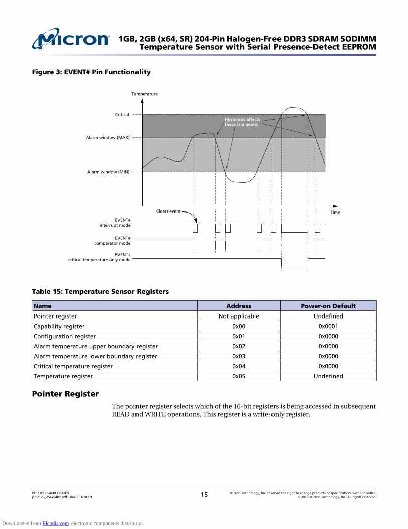
Figure 3: EVENT# Pin Functionality
Time
Temperature
Critical
Alarm window (MAX)
Alarm window (MIN)
EVENT#interrupt mode
EVENT#comparator mode
EVENT#critical temperature only mode
Clears event
Hysteresis affectsthese trip points
Table 15: Temperature Sensor Registers
Name Address Power-on Default
Pointer register Not applicable Undefined
Capability register 0x00 0x0001
Configuration register 0x01 0x0000
Alarm temperature upper boundary register 0x02 0x0000
Alarm temperature lower boundary register 0x03 0x0000
Critical temperature register 0x04 0x0000
Temperature register 0x05 Undefined
Pointer RegisterThe pointer register selects which of the 16-bit registers is being accessed in subsequentREAD and WRITE operations. This register is a write-only register.
1GB, 2GB (x64, SR) 204-Pin Halogen-Free DDR3 SDRAM SODIMMTemperature Sensor with Serial Presence-Detect EEPROM
PDF: 09005aef83364a85jsf8c128_256x64hz.pdf - Rev. C 1/10 EN 15 Micron Technology, Inc. reserves the right to change products or specifications without notice.
© 2010 Micron Technology, Inc. All rights reserved.
Downloaded from Elcodis.com electronic components distributor

Table 16: Pointer Register Bits 0–7
Bit
7 6 5 4 3 2 1 0
0 0 0 0 Registerselect
Registerselect
Registerselect
Registerselect
Table 17: Pointer Register Bits 0–2 Descriptions
Bit
Register2 1 0
0 0 0 Capability register
0 0 1 Configuration register
0 1 0 Alarm temperature upper boundary register
0 1 1 Alarm temperature lower boundary register
1 0 0 Critical temperature register
1 0 1 Temperature register
Capability RegisterThe capability register indicates the features and functionality supported by the temper-ature sensor. This register is a read-only register.
Table 18: Capability Register (Address: 0x00)
Bit
15 14 13 12 11 10 9 8
RFU RFU RFU RFU RFU RFU RFU RFU
Bit
7 6 5 4 3 2 1 0
RFU RFU RFU Temperature resolution Wider range Precision Has alarmand critical
temperature
Table 19: Capability Register Bit Description
Bit Description
0 Basic capability1: Has alarm and critical trip point capabilities
1 Accuracy0: ±2°C over the active range and ±3°C over the monitor range1: ±1°C over the active range and ±2°C over the monitor range
2 Wider range0: Temperatures lower than 0°C are clamped to a binary value of 01: Temperatures below 0°C can be read
1GB, 2GB (x64, SR) 204-Pin Halogen-Free DDR3 SDRAM SODIMMTemperature Sensor with Serial Presence-Detect EEPROM
PDF: 09005aef83364a85jsf8c128_256x64hz.pdf - Rev. C 1/10 EN 16 Micron Technology, Inc. reserves the right to change products or specifications without notice.
© 2010 Micron Technology, Inc. All rights reserved.
Downloaded from Elcodis.com electronic components distributor
Table 19: Capability Register Bit Description (Continued)
Bit Description
4:3 Temperature resolution00: 0.5°C LSB01: 0.25°C LSB10: 0.125°C LSB11: 0.0625°C LSB
15:5 0: Must be set to zero
Configuration Register
Table 20: Configuration Register (Address: 0x01)
Bit
15 14 13 12 11 10 9 8
RFU RFU RFU RFU RFU Hysteresis Shutdownmode
Bit
7 6 5 4 3 2 1 0
Critical lockbit
Alarm lock bit Clear event Event outputstatus
Event outputcontrol
Critical eventonly
Event polarity Event mode
Table 21: Configuration Register Bit Descriptions
Bit Description Notes
0 Event mode0: Comparator mode1: Interrupt mode
Event mode cannot be changed if either of the lockbits is set.
1 EVENT# polarity0: Active LOW1: Active HIGH
EVENT# polarity cannot be changed if either of thelock bits is set.
2 Critical event only0: EVENT# trips on alarm or critical temperature event1: EVENT# trips only if critical temperature is reached
3 Event output control0: Event output disabled1: Event output enabled
4 Event status0: EVENT# has not been asserted by this device1: EVENT# is being asserted due to an alarm windowor critical temperature condition
This is a read-only field in the register. The event caus-ing the event can be determined from the read tem-perature register.
5 Clear event0: No effect1: Clears the event when the temperature sensor is inthe interrupt mode
1GB, 2GB (x64, SR) 204-Pin Halogen-Free DDR3 SDRAM SODIMMTemperature Sensor with Serial Presence-Detect EEPROM
PDF: 09005aef83364a85jsf8c128_256x64hz.pdf - Rev. C 1/10 EN 17 Micron Technology, Inc. reserves the right to change products or specifications without notice.
© 2010 Micron Technology, Inc. All rights reserved.
Downloaded from Elcodis.com electronic components distributor
Table 21: Configuration Register Bit Descriptions (Continued)
Bit Description Notes
6 Alarm window lock bit0: Alarm trips are not locked and can be changed1: Alarm trips are locked and cannot be changed
7 Critical trip lock bit0: Critical trip is not locked and can be changed1: Critical trip is locked and cannot be changed
8 Shutdown mode0: Enabled1: Shutdown
The shutdown mode is a power-saving mode that dis-ables the temperature sensor.
10:9 Hysteresis enable00: Disable01: Enable at 1.5°C10: Enable at 3°C11: Enable at 6°C
When enabled, a hysteresis is applied to temperaturemovement around the trip points (see Figure 4(page 19)). As an example, if the hysteresis registeris enabled to a delta of 6°C, the preset trip points willtoggle when the temperature reaches the program-med value. These values will reset when the tempera-ture drops below the trip points minus the sethysteresis level. In this case, this would be critical tem-perature minus 6°C.
The hysteresis is applied to both the above alarm win-dow and the below alarm window bits found in theread-only temperature register (see Table 22(page 19)). EVENT# is also affected by this register.
1GB, 2GB (x64, SR) 204-Pin Halogen-Free DDR3 SDRAM SODIMMTemperature Sensor with Serial Presence-Detect EEPROM
PDF: 09005aef83364a85jsf8c128_256x64hz.pdf - Rev. C 1/10 EN 18 Micron Technology, Inc. reserves the right to change products or specifications without notice.
© 2010 Micron Technology, Inc. All rights reserved.
Downloaded from Elcodis.com electronic components distributor
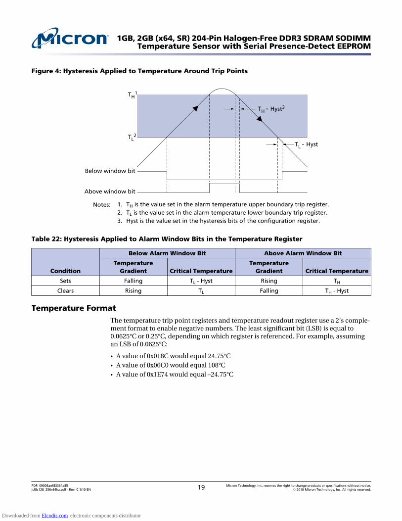
Figure 4: Hysteresis Applied to Temperature Around Trip Points
TH1
TL2
TH - Hyst3
TL - Hyst
Below window bit
Above window bit
Notes: 1. TH is the value set in the alarm temperature upper boundary trip register.2. TL is the value set in the alarm temperature lower boundary trip register.3. Hyst is the value set in the hysteresis bits of the configuration register.
Table 22: Hysteresis Applied to Alarm Window Bits in the Temperature Register
Condition
Below Alarm Window Bit Above Alarm Window Bit
TemperatureGradient Critical Temperature
TemperatureGradient Critical Temperature
Sets Falling TL - Hyst Rising TH
Clears Rising TL Falling TH - Hyst
Temperature FormatThe temperature trip point registers and temperature readout register use a 2’s comple-ment format to enable negative numbers. The least significant bit (LSB) is equal to0.0625°C or 0.25°C, depending on which register is referenced. For example, assumingan LSB of 0.0625°C:
• A value of 0x018C would equal 24.75°C
• A value of 0x06C0 would equal 108°C
• A value of 0x1E74 would equal –24.75°C
1GB, 2GB (x64, SR) 204-Pin Halogen-Free DDR3 SDRAM SODIMMTemperature Sensor with Serial Presence-Detect EEPROM
PDF: 09005aef83364a85jsf8c128_256x64hz.pdf - Rev. C 1/10 EN 19 Micron Technology, Inc. reserves the right to change products or specifications without notice.
© 2010 Micron Technology, Inc. All rights reserved.
Downloaded from Elcodis.com electronic components distributor
Temperature Trip Point RegistersThe upper and lower temperature boundary registers are used to set the maximum andminimum values of the alarm window. LSB for these registers is 0.25°C. All RFU bits inthe register will always report zero.
Table 23: Alarm Temperature Lower Boundary Register (Address: 0x02)
Bit
15 14 13 12 11 10 9 8 7 6 5 4 3 2 1 0
0 0 0 MSB LSB RFU RFU
Alarm window upper boundary temperature
Table 24: Alarm Temperature Lower Boundary Register (Address: 0x03)
Bit
15 14 13 12 11 10 9 8 7 6 5 4 3 2 1 0
0 0 0 MSB LSB RFU RFU
Alarm window lower boundary temperature
Critical Temperature RegisterThe critical temperature register is used to set the maximum temperature above thealarm window. The LSB for this register is 0.25°C. All RFU bits in the register will alwaysreport zero.
Table 25: Critical Temperature Register (Address: 0x04)
Bit
15 14 13 12 11 10 9 8 7 6 5 4 3 2 1 0
0 0 0 MSB LSB RFU RFU
Critical temperature trip point
Temperature RegisterThe temperature register is a read-only register that provides the current temperaturedetected by the temperature sensor. The LSB for this register is 0.0625°C with a resolu-tion of 0.0625°C. The most significant bit (MSB) is 128°C in the readout section of thisregister.
The upper three bits of the register are used to monitor the trip points that are set in theprevious three registers.
1GB, 2GB (x64, SR) 204-Pin Halogen-Free DDR3 SDRAM SODIMMTemperature Sensor with Serial Presence-Detect EEPROM
PDF: 09005aef83364a85jsf8c128_256x64hz.pdf - Rev. C 1/10 EN 20 Micron Technology, Inc. reserves the right to change products or specifications without notice.
© 2010 Micron Technology, Inc. All rights reserved.
Downloaded from Elcodis.com electronic components distributor
Table 26: Temperature Register (Address: 0x05)
Bit
15 14 13 12 11 10 9 8 7 6 5 4 3 2 1 0
Abovecritical
trip
Abovealarm
window
Belowalarm
window
MSB LSB
Temperature
Table 27: Temperature Register Bit Descriptions
Bit Description
13 Below alarm window0: Temperature is equal to or above the lower boundary1: Temperature is below alarm window
14 Above alarm window0: Temperature is equal to or below the upper boundary1: Temperature is above alarm window
15 Above critical trip point0: Temperature is below critical trip point1: Temperature is above critical trip point
Serial Presence-Detect DataFor the latest serial presence-detect data, refer to Micron's SPD page:www.micron.com/SPD.
1GB, 2GB (x64, SR) 204-Pin Halogen-Free DDR3 SDRAM SODIMMTemperature Sensor with Serial Presence-Detect EEPROM
PDF: 09005aef83364a85jsf8c128_256x64hz.pdf - Rev. C 1/10 EN 21 Micron Technology, Inc. reserves the right to change products or specifications without notice.
© 2010 Micron Technology, Inc. All rights reserved.
Downloaded from Elcodis.com electronic components distributor
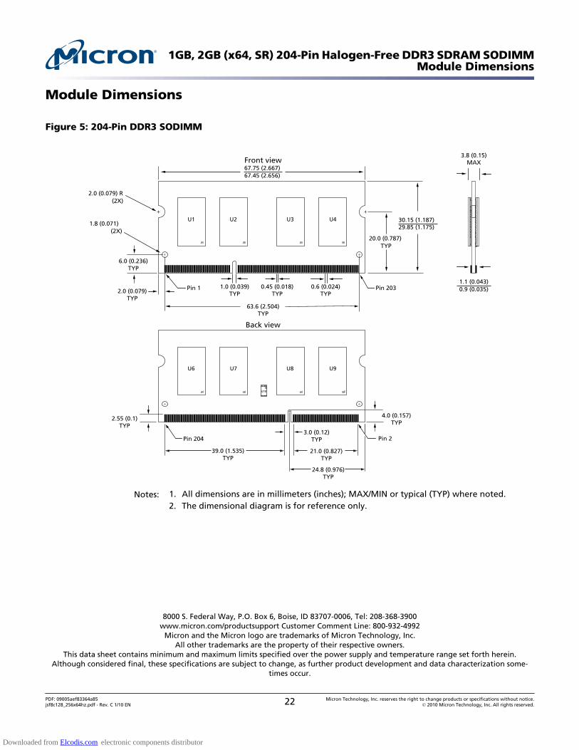
Module Dimensions
Figure 5: 204-Pin DDR3 SODIMM
3.8 (0.15)
MAX
Pin 1
67.75 (2.667)67.45 (2.656)
20.0 (0.787)TYP
1.8 (0.071)(2X)
0.6 (0.024) TYP
0.45 (0.018) TYP
2.0 (0.079) R(2X)
Pin 203
Pin 204 Pin 2
Front view
2.0 (0.079) TYP
6.0 (0.236) TYP
63.6 (2.504) TYP
2.55 (0.1) TYP
1.0 (0.039) TYP
30.15 (1.187)29.85 (1.175)
Back view
1.1 (0.043)0.9 (0.035)
39.0 (1.535) TYP
21.0 (0.827) TYP
3.0 (0.12) TYP
4.0 (0.157) TYP
24.8 (0.976) TYP
U1 U2 U3 U4
U6 U7 U8 U9
U10
Notes: 1. All dimensions are in millimeters (inches); MAX/MIN or typical (TYP) where noted.2. The dimensional diagram is for reference only.
8000 S. Federal Way, P.O. Box 6, Boise, ID 83707-0006, Tel: 208-368-3900www.micron.com/productsupport Customer Comment Line: 800-932-4992
Micron and the Micron logo are trademarks of Micron Technology, Inc.All other trademarks are the property of their respective owners.
This data sheet contains minimum and maximum limits specified over the power supply and temperature range set forth herein.Although considered final, these specifications are subject to change, as further product development and data characterization some-
times occur.
1GB, 2GB (x64, SR) 204-Pin Halogen-Free DDR3 SDRAM SODIMMModule Dimensions
PDF: 09005aef83364a85jsf8c128_256x64hz.pdf - Rev. C 1/10 EN 22 Micron Technology, Inc. reserves the right to change products or specifications without notice.
© 2010 Micron Technology, Inc. All rights reserved.
Downloaded from Elcodis.com electronic components distributor