dc to 50 mhz, quad i/q demodulator and phase shifter data ...€¦ · dc to 50 mhz, quad i/q...
TRANSCRIPT
DC to 50 MHz, Quad I/Q Demodulator and Phase Shifter
Data Sheet AD8339
Rev. B Information furnished by Analog Devices is believed to be accurate and reliable. However, no responsibility is assumed by Analog Devices for its use, nor for any infringements of patents or other rights of third parties that may result from its use. Specifications subject to change without notice. No license is granted by implication or otherwise under any patent or patent rights of Analog Devices. Trademarks and registered trademarks are the property of their respective owners.
One Technology Way, P.O. Box 9106, Norwood, MA 02062-9106, U.S.A. Tel: 781.329.4700 www.analog.com Fax: 781.461.3113 ©2007–2012 Analog Devices, Inc. All rights reserved.
FEATURES Quad integrated I/Q demodulator 16 phase select on each output (22.5° per step) Quadrature demodulation accuracy
Phase accuracy: ±1° Amplitude imbalance: ±0.05 dB
Bandwidth 4LO: LF to 200 MHz RF: LF to 50 MHz Baseband: determined by external filtering
Output dynamic range: 160 dB/Hz LO drive: >0 dBm (50 Ω), single-ended sine wave Supply: ±5 V Power consumption: 73 mW/channel (290 mW total) Power-down via SPI (each channel and complete chip)
APPLICATIONS Medical imaging (CW ultrasound beamforming) Phased array systems
Radar Adaptive antennas
Communication receivers
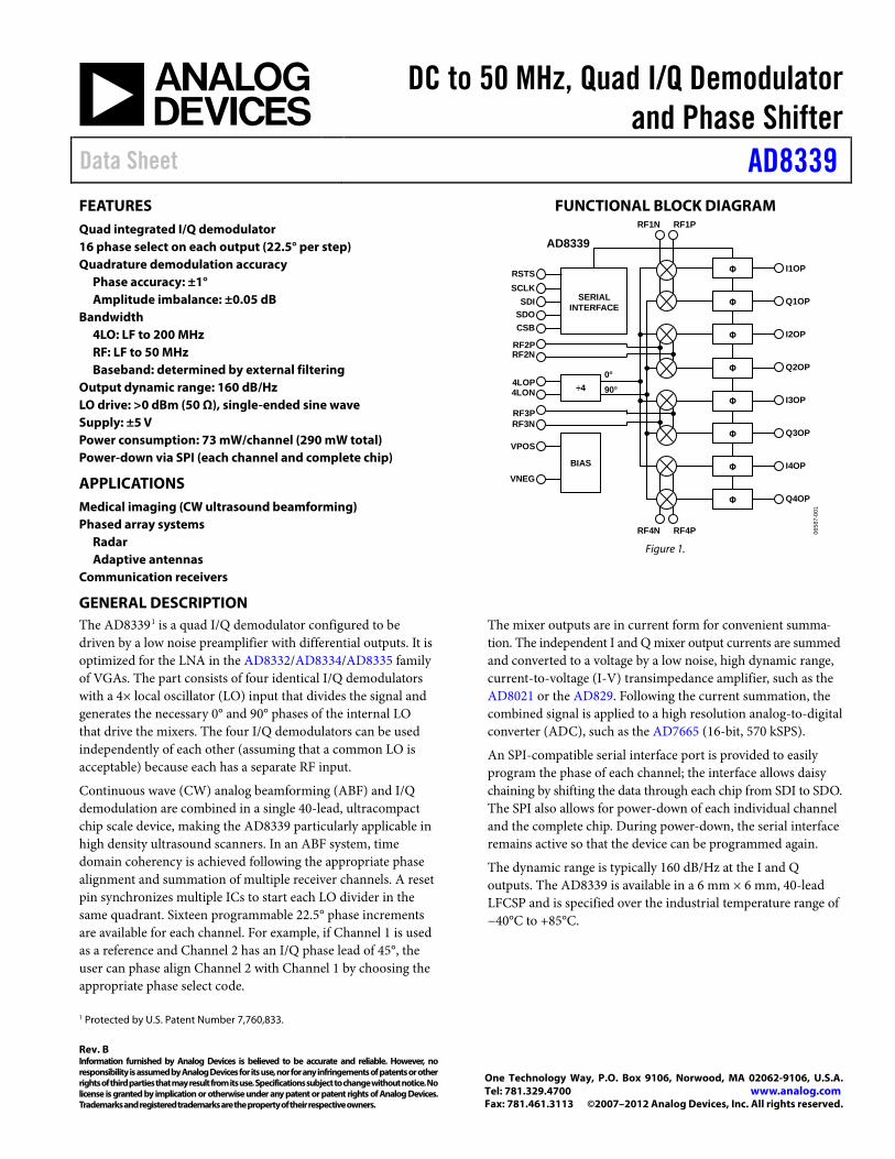
FUNCTIONAL BLOCK DIAGRAM
AD8339
SCLK
SDOCSB
RF2PRF2N
4LOP4LON
RF3PRF3N
VPOS
VNEG
SDI
I1OP
RF4PRF4N
RF1PRF1N
I2OP
Q2OP
I3OP
Q3OP
I4OP
Q4OP
Q1OP
RSTS Φ
Φ
Φ
Φ
Φ
Φ
Φ
Φ
SERIALINTERFACE
÷4
BIAS
0°90°
0658
7-00
1
Figure 1.
GENERAL DESCRIPTION The AD83391 is a quad I/Q demodulator configured to be driven by a low noise preamplifier with differential outputs. It is optimized for the LNA in the AD8332/AD8334/AD8335 family of VGAs. The part consists of four identical I/Q demodulators with a 4× local oscillator (LO) input that divides the signal and generates the necessary 0° and 90° phases of the internal LO that drive the mixers. The four I/Q demodulators can be used independently of each other (assuming that a common LO is acceptable) because each has a separate RF input.
Continuous wave (CW) analog beamforming (ABF) and I/Q demodulation are combined in a single 40-lead, ultracompact chip scale device, making the AD8339 particularly applicable in high density ultrasound scanners. In an ABF system, time domain coherency is achieved following the appropriate phase alignment and summation of multiple receiver channels. A reset pin synchronizes multiple ICs to start each LO divider in the same quadrant. Sixteen programmable 22.5° phase increments are available for each channel. For example, if Channel 1 is used as a reference and Channel 2 has an I/Q phase lead of 45°, the user can phase align Channel 2 with Channel 1 by choosing the appropriate phase select code. 1 Protected by U.S. Patent Number 7,760,833.
The mixer outputs are in current form for convenient summa-tion. The independent I and Q mixer output currents are summed and converted to a voltage by a low noise, high dynamic range, current-to-voltage (I-V) transimpedance amplifier, such as the AD8021 or the AD829. Following the current summation, the combined signal is applied to a high resolution analog-to-digital converter (ADC), such as the AD7665 (16-bit, 570 kSPS).
An SPI-compatible serial interface port is provided to easily program the phase of each channel; the interface allows daisy chaining by shifting the data through each chip from SDI to SDO. The SPI also allows for power-down of each individual channel and the complete chip. During power-down, the serial interface remains active so that the device can be programmed again.
The dynamic range is typically 160 dB/Hz at the I and Q outputs. The AD8339 is available in a 6 mm × 6 mm, 40-lead LFCSP and is specified over the industrial temperature range of −40°C to +85°C.

AD8339 Data Sheet
Rev. B | Page 2 of 36
TABLE OF CONTENTS Features .............................................................................................. 1 Applications ....................................................................................... 1 Functional Block Diagram .............................................................. 1 General Description ......................................................................... 1 Revision History ............................................................................... 2 Specifications ..................................................................................... 3 Absolute Maximum Ratings ............................................................ 5
ESD Caution .................................................................................. 5 Pin Configuration and Function Descriptions ............................. 6 Equivalent Input Circuits ................................................................ 7 Typical Performance Characteristics ............................................. 8 Test Circuits ..................................................................................... 14 Theory of Operation ...................................................................... 18
Quadrature Generation ............................................................. 19 I/Q Demodulator and Phase Shifter ........................................ 19
Dynamic Range and Noise ........................................................ 19 Multichannel Summation ......................................................... 20
Serial Interface ................................................................................ 23 ENBL Bits .................................................................................... 23
Applications Information .............................................................. 24 Logic Inputs and Interfaces ....................................................... 24 Reset Input .................................................................................. 24 LO Input ...................................................................................... 24
Evaluation Board ............................................................................ 25 Connections to the Board ......................................................... 26 Test Configurations .................................................................... 26 AD8339-EVALZ Artwork ......................................................... 33
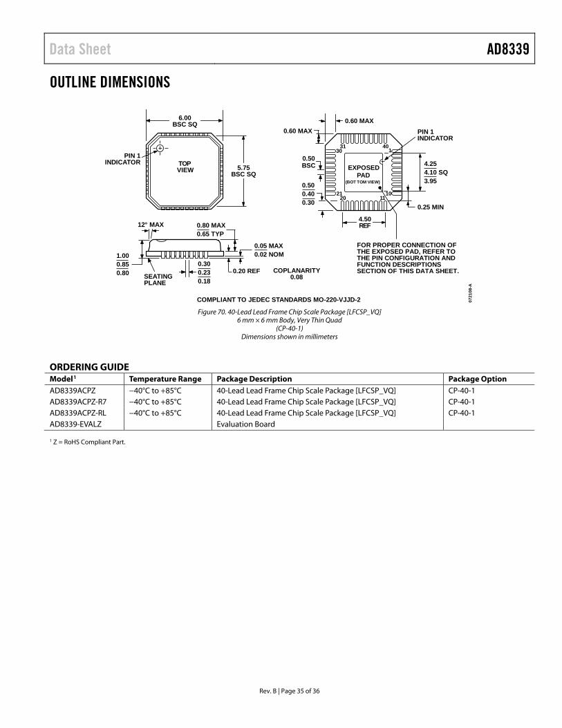
Outline Dimensions ....................................................................... 35 Ordering Guide .......................................................................... 35
REVISION HISTORY 7/12—Rev. A to Rev. B
Changes to Figure 1 and General Description Section ................ 1
2/09—Rev. 0 to Rev. A
Change to Figure 1 ........................................................................... 1 Change to Table 2 ............................................................................. 5 Added Exposed Pad Notation to Figure 2; Changes to Table 3 ............................................................................ 6 Changes to Figure 3; Added Figure 4; Renumbered Sequentially ................................................................ 7 Changes to Theory of Operation Section .................................... 18 Changes to Dynamic Range and Noise Section, ........................ 20 Changes to Channel Summing Section ....................................... 21 Added Figure 55 .............................................................................. 22 Changes to Serial Interface Section, ENBL Bits Section, Figure 56, and Figure 57 ................................................................ 23
Changes to Evaluation Board Section and Figure 58 ................ 25 Changes to Connections to the Board Section and Table 5 ...... 26 Changes to Figure 60 ...................................................................... 27 Changes to Figure 61 ...................................................................... 28 Changes to Table 7 .......................................................................... 29 Changes to Figure 63 ...................................................................... 30 Changes to Figure 64 ...................................................................... 31 Changes to Figure 65 ...................................................................... 32 Changes to Figure 66 and Figure 67............................................. 33 Changes to Figure 68 and Figure 69............................................. 34 Deleted Table 8 ................................................................................ 35 Updated Outline Dimensions ....................................................... 35
8/07—Revision 0: Initial Version
Data Sheet AD8339
Rev. B | Page 3 of 36
SPECIFICATIONS VS = ±5 V, TA = 25°C, 4fLO = 20 MHz, fRF = 5.01 MHz, fBB = 10 kHz, PLO ≥ 0 dBm, per channel performance, dBm (50 Ω), unless otherwise noted. Single-channel AD8021 LPF values: RFILT = 787 Ω and CFILT = 2.2 nF (see Figure 53).
Table 1. Parameter Test Conditions/Comments Min Typ Max Unit OPERATING CONDITIONS
Local Oscillator (LO) Frequency Range
4× internal LO at Pin 4LOP and Pin 4LON, square wave drive via LVDS (see Figure 64)
0.01 200 MHz
RF Frequency Range Mixing DC 50 MHz Baseband Bandwidth Limited by external filtering DC 50 MHz LO Input Level 0 13 dBm Supply Voltage (VS) ±4.5 ±5.0 ±5.5 V Temperature Range −40 +85 °C
DEMODULATOR PERFORMANCE Input Impedance RF, differential 25||10 kΩ||pF LO, differential 100||4 kΩ||pF Transconductance Demodulated IOUT/VIN; each Ix or Qx output after low-pass
filtering measured from RF inputs, all phases 1.15 mS
Dynamic Range IP1dB − input referred noise (dBm) 160 dB/Hz Maximum Input Swing Differential; inputs biased at 2.5 V; Pin RFxP, Pin RFxN 2.8 V p-p Peak Output Current (No Filtering) 0° phase shift ±2.4 mA 45° phase shift ±3.1 mA Input P1dB Ref = 50 Ω 14.8 dBm Ref = 1 V rms 1.85 dBV Third-Order Intermodulation (IM3) fRF1 = 5.010 MHz, fRF2 = 5.015 MHz, fLO = 5.023 MHz
Equal Input Levels Baseband tones: 0 dBm @ 8 kHz and 13 kHz −60 dBc Unequal Input Levels Baseband tones: −1 dBm @ 8 kHz and −31 dBm @ 13 kHz −66 dBc
Third-Order Input Intercept (IIP3) fRF1 = 5.010 MHz, fRF2 = 5.015 MHz, fLO = 5.023 MHz 31 dBm LO Leakage Measured at RF inputs, worst phase, measured into 50 Ω −118 dBm Measured at baseband outputs, worst phase, AD8021
disabled, measured into 50 Ω −68 dBm
Conversion Gain All codes, see Figure 42 −1.3 dB Input Referred Noise Output noise/conversion gain (see Figure 47) 11.8 nV/√Hz Output Current Noise Output noise/RFILT 12.9 pA/√Hz Noise Figure With AD8334 LNA RS = 50 Ω, RFB = ∞ 8.4 dB RS = 50 Ω, RFB = 1.1 kΩ 9.1 dB RS = 50 Ω, RFB = 274 Ω 11.5 dB Bias Current Pin 4LOP and Pin 4LON −3 μA Pin RFxP and Pin RFxN −45 μA LO Common-Mode Range Pin 4LOP and Pin 4LON (each pin) 0.2 3.8 V RF Common-Mode Voltage For maximum differential swing; Pin RFxP and Pin RFxN
(dc-coupled to AD8334 LNA output)
2.5 V
Output Compliance Range Pin IxOP and Pin QxOP −1.5 +0.7 V PHASE ROTATION PERFORMANCE One channel is reference; others are stepped
Phase Increment 16 phase steps per channel 22.5 Degrees Quadrature Phase Error Ix to Qx; all phases, 1σ −2 ±1 +2 Degrees I/Q Amplitude Imbalance Ix to Qx; all phases, 1σ ±0.05 dB Channel-to-Channel Matching Phase match I-to-I and Q-to-Q; −40°C < TA < +85°C ±1 Degrees Amplitude match I-to-I and Q-to-Q; −40°C < TA < +85°C ±0.1 dB

AD8339 Data Sheet
Rev. B | Page 4 of 36
Parameter Test Conditions/Comments Min Typ Max Unit LOGIC INTERFACES
Pin SDI, Pin CSB, Pin SCLK, Pin RSET Logic Level High 1.5 V Logic Level Low 0.9 V
Pin RSTS Logic Level High 1.8 V Logic Level Low 1.2 V
Bias Current Logic high (pulled to 5 V) 0.5 μA Logic low (pulled to GND) 0 μA Input Resistance 4 MΩ LO Divider RSET Setup Time RSET rising or falling edge to 4LOP or 4LON (differential)
rising edge 5 ns
LO Divider RSET High Pulse Width 20 ns LO Divider RSET Response Time 200 ns Phase Response Time Measured from CSB going high 5 μs Enable Response Time Measured from CSB going high (with 0.1 μF capacitor on
Pin LODC); no channel enabled 12 15 μs
At least one channel enabled 500 ns Output Pin SDO loaded with 5 pF and next SDI input
Logic Level High 1.7 1.9 V Logic Level Low 0.2 0.5 V
SPI TIMING CHARACTERISTICS Pin SDI, Pin SDO, Pin CSB, Pin SCLK, Pin RSTS SCLK Frequency fCLK 10 MHz CSB Fall to SCLK Setup Time t1 0 ns SCLK High Pulse Width t2 10 ns SCLK Low Pulse Width t3 10 ns Data Access Time (SDO) After SCLK
Rising Edge t4 100 ns
Data Setup Time Before SCLK Rising Edge
t5 2 ns
Data Hold Time After SCLK Rising Edge
t6 2 ns
SCLK Rise to CSB Rise Hold Time t7 15 ns CSB Rise to SCLK Rise Hold Time t8 0 ns
POWER SUPPLY Pin VPOS, Pin VNEG Supply Voltage ±4.5 ±5.0 ±5.5 V Current VPOS, all phase bits = 0 35 mA VNEG, all phase bits = 0 −18 mA
Over Temperature, −40°C < TA < +85°C
VPOS, all phase bits = 0 33 36 mA
VNEG, all phase bits = 0 −19 −17 mA Quiescent Power Per channel, all phase bits = 0 66 mW Per channel maximum (depends on phase bits) 88 mW Disable Current All channels disabled; SPI stays on 2.75 mA PSRR VPOS to Ix/Qx outputs, @ 10 kHz −85 dB VNEG to Ix/Qx outputs, @ 10 kHz −85 dB

Data Sheet AD8339
Rev. B | Page 5 of 36
ABSOLUTE MAXIMUM RATINGS Table 2. Parameter Rating Voltages
Supply Voltage (VS) ±6 V RF Inputs 6 V to GND 4LO Inputs 6 V to GND Outputs (IxOP, QxOP) +0.7 V to −6 V Digital Inputs +6 V to −1.4 V SDO Output 6 V to GND LODC Pin VPOS − 1.5 V to +6 V
Thermal Data (4-Layer JEDEC Board, No Airflow, Exposed Pad Soldered to PCB)
θJA 32.2°C/W θJB 17.8°C/W θJC 2.7°C/W ψJT 0.3°C/W ψJB 16.7°C/W
Maximum Junction Temperature 150°C Maximum Power Dissipation
(Exposed Pad Soldered to PCB) 2 W
Operating Temperature Range −40°C to +85°C Storage Temperature Range −65°C to +150°C Lead Temperature (Soldering, 60 sec) 300°C
Stresses above those listed under Absolute Maximum Ratings may cause permanent damage to the device. This is a stress rating only; functional operation of the device at these or any other conditions above those indicated in the operational section of this specification is not implied. Exposure to absolute maximum rating conditions for extended periods may affect device reliability.
ESD CAUTION
AD8339 Data Sheet
Rev. B | Page 6 of 36
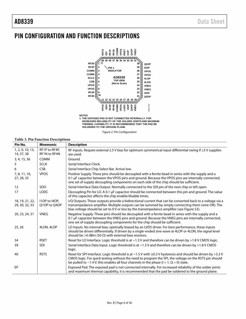
PIN CONFIGURATION AND FUNCTION DESCRIPTIONS
0658
7-00
2
8765
1
432 29
303132
28
34 33
27
1413 171211 1815 16 20
37 35
1921222324
PIN 1INDICATOR
AD8339TOP VIEW
(Not to Scale)
109
3839 3640
2526
RF2NRF2P
SCLKCSB
COMMCOMM
VPOSVPOSRF3PRF3N
RST
SSD
I
CO
MM
VPO
S
RF1
PR
F1N
RSE
TI1
OP
Q1O
PVN
EG
VPO
SSD
O
CO
MM
VPO
S
RF4
PR
F4N
LOD
CI4
OP
Q4O
PVN
EG
Q2OPI2OP
4LOP4LON
VPOSVPOS
VNEGVNEGI3OPQ3OP
NOTES1. THE EXPOSED PAD IS NOT CONNECTED INTERNALLY. FOR INCREASED RELIABILITY OF THE SOLDER JOINTS AND MAXIMUM THERMAL CAPABILITY, IT IS RECOMMENDED THAT THE PAD BE SOLDERED TO THE GROUND PLANE.
Figure 2. Pin Configuration
Table 3. Pin Function Descriptions Pin No. Mnemonic Description 1, 2, 9, 10, 13, 14, 37, 38
RF1P to RF4P, RF1N to RF4N
RF Inputs. Require external 2.5 V bias for optimum symmetrical input differential swing if ±5 V supplies are used.
3, 4, 15, 36 COMM Ground. 5 SCLK Serial Interface Clock. 6 CSB Serial Interface Chip Select Bar. Active low. 7, 8, 11, 16, 27, 28, 35
VPOS Positive Supply. These pins should be decoupled with a ferrite bead in series with the supply and a 0.1 μF capacitor between the VPOS pins and ground. Because the VPOS pins are internally connected, one set of supply decoupling components on each side of the chip should be sufficient.
12 SDO Serial Interface Data Output. Normally connected to the SDI pin of the next chip or left open. 17 LODC Decoupling Pin for LO. A 0.1 μF capacitor should be connected between this pin and ground. The value
of this capacitor affects the chip enable/disable times. 18, 19, 21, 22, 29, 30, 32, 33
I1OP to I4OP, Q1OP to Q4OP
I/Q Outputs. These outputs provide a bidirectional current that can be converted back to a voltage via a transimpedance amplifier. Multiple outputs can be summed by simply connecting them (wire-OR). The bias voltage should be set to 0 V or less by the transimpedance amplifier (see Figure 53).
20, 23, 24, 31 VNEG Negative Supply. These pins should be decoupled with a ferrite bead in series with the supply and a 0.1 μF capacitor between the VNEG pins and ground. Because the VNEG pins are internally connected, one set of supply decoupling components for the chip should be sufficient.
25, 26 4LON, 4LOP LO Inputs. No internal bias; optimally biased by an LVDS driver. For best performance, these inputs should be driven differentially. If driven by a single-ended sine wave at 4LOP or 4LON, the signal level should be >0 dBm (50 Ω) with external bias resistors.
34 RSET Reset for LO Interface. Logic threshold is at ~1.3 V and therefore can be driven by >1.8 V CMOS logic. 39 SDI Serial Interface Data Input. Logic threshold is at ~1.3 V and therefore can be driven by >1.8 V CMOS
logic. 40 RSTS Reset for SPI Interface. Logic threshold is at ~1.5 V with ±0.3 V hysteresis and should be driven by >3.3 V
CMOS logic. For quick testing without the need to program the SPI, the voltage on the RSTS pin should be pulled to −1.4 V; this enables all four channels in the phase (I = 1, Q = 0) state.
EP Exposed Pad. The exposed pad is not connected internally. For increased reliability of the solder joints and maximum thermal capability, it is recommended that the pad be soldered to the ground plane.
Data Sheet AD8339
Rev. B | Page 7 of 36
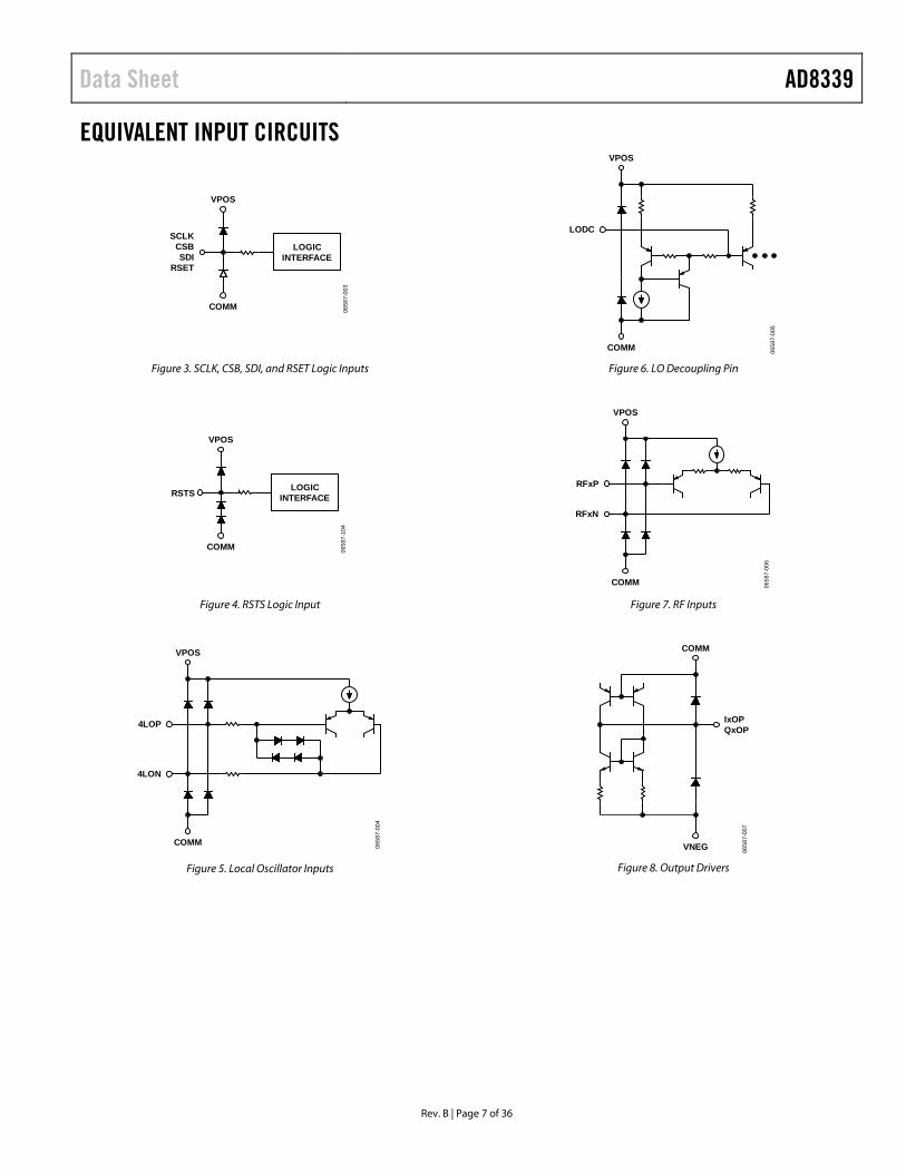
EQUIVALENT INPUT CIRCUITS
0658
7-00
3
VPOS
SCLKCSBSDI
RSET
COMM
LOGICINTERFACE
Figure 3. SCLK, CSB, SDI, and RSET Logic Inputs
0658
7-10
4
VPOS
RSTS
COMM
LOGICINTERFACE
Figure 4. RSTS Logic Input
0658
7-00
4
4LOP
4LON
VPOS
COMM
Figure 5. Local Oscillator Inputs
0658
7-00
5
LODC
VPOS
COMM
Figure 6. LO Decoupling Pin
0658
7-00
6
RFxP
RFxN
VPOS
COMM
Figure 7. RF Inputs
0658
7-00
7
IxOPQxOP
VNEG
COMM
Figure 8. Output Drivers
AD8339 Data Sheet
Rev. B | Page 8 of 36
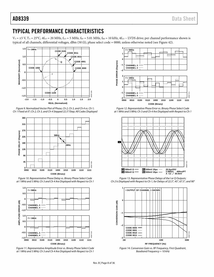
TYPICAL PERFORMANCE CHARACTERISTICS VS = ±5 V, TA = 25°C, 4fLO = 20 MHz, fLO = 5 MHz, fRF = 5.01 MHz, fBB = 10 kHz, 4fLO − LVDS drive; per channel performance shown is typical of all channels, differential voltages, dBm (50 Ω), phase select code = 0000, unless otherwise noted (see Figure 42).
1.5
0.5
0
1.0
–1.5
–0.5
–1.0
–2.0 –1.5 1.5–1.0 1.0–0.5 0 0.5 2.0
0658
7-00
8
REAL (Normalized)
IMA
GIN
AR
Y (N
orm
aliz
ed)
f = 1MHz
CODE 1000
CODE 1100
CODE 0100CODE 0011
I
Q
CODE 0010
CODE 0000
CODE 0001
Figure 9. Normalized Vector Plot of Phase, Ch 2, Ch 3, and Ch 4 vs. Ch 1; Ch 1 Fixed at 0°; Ch 2, Ch 3, and Ch 4 Stepped 22.5°/Step; All Codes Displayed
360
00000 1111
0658
7-00
9
CODE (Binary)
PHA
SE D
ELA
Y (D
egre
es)
315
270
225
180
135
90
45
0010 0100 0110 1000 1010 1100 1110
5MHz
1MHz
Figure 10. Representative Phase Delay vs. Binary Phase Select Code
at 1 MHz and 5 MHz; Ch 3 and Ch 4 Are Displayed with Respect to Ch 1
1.0
–1.00000 1111
0658
7-01
0
CODE (Binary)
AM
PLIT
UD
E ER
RO
R (d
B)
0010 0100 0110 1000 1010 1100 1110
0.5
0
–0.5
–1.0
1.0
0.5
0
–0.5
f = 1MHz
f = 5MHz
CHANNEL 3CHANNEL 4
CHANNEL 3CHANNEL 4
Figure 11. Representative Amplitude Error vs. Binary Phase Select Code at 1 MHz and 5 MHz; Ch 3 and Ch 4 Are Displayed with Respect to Ch 1
2
–20000 1111
0658
7-01
1
CODE (Binary)
PHA
SE E
RR
OR
(Deg
rees
)
0010 0100 0110 1000 1010 1100 1110
1
0
–1
–2
2
1
0
–1
f = 1MHz
f = 5MHz
CHANNEL 3CHANNEL 4
CHANNEL 3CHANNEL 4
Figure 12. Representative Phase Error vs. Binary Phase Select Code
at 1 MHz and 5 MHz; Ch 3 and Ch 4 Are Displayed with Respect to Ch 1
0658
7-01
2
21
20.0µs/DIV2.5MS/s 400ns/PTA C2 30.0mV
R1 500mV 20µsR2 500mV 20µs
C2 500mV ΩC4 500mV Ω
Figure 13. Representative Phase Delays of the I or Q Outputs;
Ch 2 Is Displayed with Respect to Ch 1, for Delays of 22.5°, 45°, 67.5°, and 90°
1
0
–3
–2
–1
1M 50M10M
0658
7-01
3
RF FREQUENCY (Hz)
CO
NVE
RSI
ON
GA
IN (d
B)
I OUTPUT OF CHANNEL 1 SHOWN
CODE 0000CODE 0001
CODE 0011CODE 0010
Figure 14. Conversion Gain vs. RF Frequency, First Quadrant,
Baseband Frequency = 10 kHz
Data Sheet AD8339
Rev. B | Page 9 of 36
8
–8 0658
7-01
4
RF FREQUENCY (Hz)
QU
AD
RA
TUR
E PH
ASE
ER
RO
R (D
egre
es)
6
4
2
0
–2
–4
–6
1M 50M10M
Figure 15. Representative Range of Quadrature Phase Error vs. RF Frequency
for All Channels and Codes
2.0
–2.0 0658
7-01
5
BASEBAND FREQUENCY (Hz)
QU
AD
RA
TUR
E PH
ASE
ER
RO
R (D
egre
es)
1.5
1.0
0.5
0
–0.5
–1.0
–1.5
100 100k10k1k
Figure 16. Representative Range of Quadrature Phase Error vs. Baseband
Frequency for All Channels and Codes (See Figure 44)
0.5
–0.5 0658
7-01
6
RF FREQUENCY (Hz)
I/Q A
MPL
ITU
DE
IMB
ALA
NC
E (d
B)
1M 50M10M
0.3
0.2
0.1
0
–0.1
–0.2
–0.3
–0.4
0.4
Figure 17. Representative Range of I/Q Amplitude Imbalance vs.
RF Frequency for All Channels and Codes
0.5
–0.5 0658
7-01
7
BASEBAND FREQUENCY (Hz)
I/Q A
MPL
ITU
DE
IMB
ALA
NC
E (d
B)
100 100k
0.3
0.2
0.1
0
–0.1
–0.2
–0.3
–0.4
0.4
1k 10k
Figure 18. Representative Range of I/Q Amplitude Imbalance vs. Baseband
Frequency for All Channels and Codes (See Figure 44)
3
–3 0658
7-01
8
RF FREQUENCY (Hz)
AM
PLIT
UD
E M
ATC
H (d
B)
1M 50M10M
1
0
–1
–2
2
fBB = 10kHz
Figure 19. Typical Channel-to-Channel Amplitude Match vs. RF Frequency,
First Quadrant, over the Range of Operating Temperatures
8
–8 0658
7-01
9
RF FREQUENCY (Hz)
PHA
SE E
RR
OR
(Deg
rees
)
1M 50M10M
4
2
0
–2
–4
–6
6fBB = 10kHz
Figure 20. Typical Channel-to-Channel Phase Error vs. RF Frequency,
First Quadrant, over the Range of Operating Temperatures

AD8339 Data Sheet
Rev. B | Page 10 of 36
1.4
1.3
0.8
0.9
1.0
1.1
1.2
1M 50M10M
0658
7-02
0
RF FREQUENCY (Hz)
TRA
NSC
ON
DU
CTA
NC
E (m
S)
I OUTPUT OF CHANNEL 1 SHOWNTRANSCONDUCTANCE = [(VBB/787Ω)/VRF]
PHASE DELAY = 22.5°
PHASE DELAY = 67.5°PHASE DELAY = 45°
PHASE DELAY = 0°
Figure 21. Transconductance vs. RF Frequency
for First Quadrant Phase Delays
10
–700 5.0
0658
7-02
1
COMMON-MODE VOLTAGE (V)
CO
NVE
RSI
ON
GA
IN (d
B)
0
–10
–20
–30
–40
–50
–60
0.5 1.0 1.5 2.0 2.5 3.0 3.5 4.0 4.5
+85°C+25°C–40°C
Figure 22. LO Common-Mode Range at Three Temperatures
20
01M 50M10M
0658
7-02
2
RF FREQUENCY (Hz)
IP1d
B (d
Bm
)
18
16
14
12
10
8
6
4
2
Figure 23. Representative Range of IP1dB vs. RF Frequency,
Baseband Frequency = 10 kHz, First Quadrant (See Figure 43)
0
–701M 50M10M
0658
7-02
3
RF FREQUENCY (Hz)
IM3
(dB
c)
–10
–20
–30
–40
–50
–60
0dBm
IM3 PRODUCTS133 8 18
LO = 5.023MHzRF1 = 5.015MHzRF2 = 5.010MHz
Figure 24. Representative Range of IM3 vs. RF Frequency, First Quadrant
(See Figure 49)
35
01M 50M10M
0658
7-02
4
RF FREQUENCY (Hz)
OIP
3 (d
Bm
)
30
25
20
15
10
5
Figure 25. Representative Range of OIP3 vs. RF Frequency, First Quadrant
(See Figure 49)
35
01k 100k
0658
7-02
5
BASEBAND FREQUENCY (Hz)
OIP
3 (d
Bm
)
30
25
20
15
10
5
10k
Figure 26. Representative Range of OIP3 vs. Baseband Frequency
(See Figure 48)

Data Sheet AD8339
Rev. B | Page 11 of 36
0
–901M 50M10M
0658
7-02
6
RF FREQUENCY (Hz)
LO L
EAK
AG
E (d
Bm
)
–10
–20
–30
–40
–50
–60
–70
–80
LO LEVEL = 0dBm
Figure 27. Representative Range of LO Leakage vs. RF Frequency
at I and Q Outputs
0
–1401M 50M10M
0658
7-02
7
RF FREQUENCY (Hz)
LO L
EAK
AG
E (d
Bm
)
–20
–40
–60
–80
–100
–120
LO LEVEL = 0dBm
Figure 28. Representative Range of LO Leakage vs. RF Frequency at RF Inputs
16
01M 50M10M
0658
7-02
8
RF FREQUENCY (Hz)
NO
ISE
(nV/
√Hz)
NO
ISE
(dB
m)
14
10
12
8
6
4
2
–142.9
–144.1
–147.0
–145.4
–148.9
–151.4
–154.9
–161.0
Figure 29. Representative Range of Input Referred Noise vs. RF Frequency
20
01M 50M10M
0658
7-02
9
RF FREQUENCY (Hz)
NO
ISE
FIG
UR
E (d
B) 14
16
18
10
12
8
6
4
2
Figure 30. Noise Figure vs. RF Frequency (When Driven by AD8334 LNA)
172
162
152
154
156
158
160
1M 50M10M
0658
7-03
0
RF FREQUENCY (Hz)
DYN
AM
IC R
AN
GE
(dB
)
170
168
164
166
Q1 + Q2 + Q3 + Q4I1 + I2 + I3 + I4
Q2
Q4Q3
Q1
Q3 + Q4Q1 + Q2
I3 + I4I1 + I2
Figure 31. Dynamic Range vs. RF Frequency, IP1dB Minus Noise Level
0
–16
–8
–3.5 1.0
0658
7-03
1
VOLTAGE (V)
GA
IN (d
B)
–2
–4
–6
–10
–12
–14
–3.0 –2.5 –2.0 –1.5 –1.0 –0.5 0 0.5
DELAY = 22.5°
DELAY = 67.5°DELAY = 45°
DELAY = 0°
GAIN = VBB/VRF
Figure 32. Output Compliance Range for Four Values of Phase Delay
(See Figure 50)
AD8339 Data Sheet
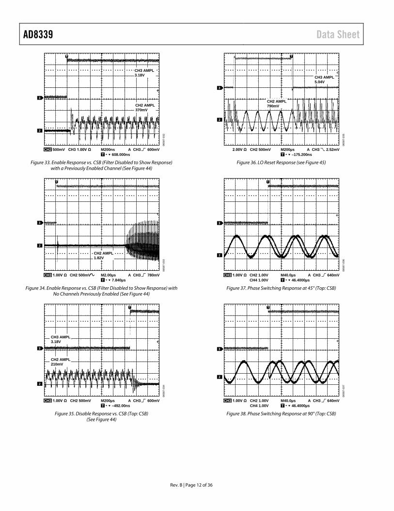
Rev. B | Page 12 of 36
0658
7-03
2
CH2 500mV CH3 1.00V Ω M200ns A CH3 600mV
2
T 608.000ns
3
T
CH2 AMPL370mV
CH3 AMPL3.18V
Figure 33. Enable Response vs. CSB (Filter Disabled to Show Response)
with a Previously Enabled Channel (See Figure 44) 06
587-
033
CH3 1.00V Ω CH2 500mV M2.00µs A CH3 780mV
2
T 7.840µs
3
CH2 AMPL1.82V
Figure 34. Enable Response vs. CSB (Filter Disabled to Show Response) with
No Channels Previously Enabled (See Figure 44)
0658
7-03
4
CH3 1.00V Ω CH2 500mV M200µs A CH3 600mV
2
T –492.00ns
3
CH2 AMPL210mV
CH3 AMPL3.18V
Figure 35. Disable Response vs. CSB (Top: CSB)
(See Figure 44)
0658
7-03
5
CH3 2.00V Ω CH2 500mV M200µs A CH3 2.52mV
2
T –175.200ns
3
CH2 AMPL790mV
CH3 AMPL5.04V
Figure 36. LO Reset Response (see Figure 45)
0658
7-03
6
CH3 1.00V Ω CH2 1.00VCH4 1.00V
M40.0µs A CH3 640mV
2
T 46.4000µs
3
Figure 37. Phase Switching Response at 45° (Top: CSB)
0658
7-03
7
CH3 1.00V Ω CH2 1.00VCH4 1.00V
M40.0µs A CH3 640mV
2
T 46.4000µs
3
Figure 38. Phase Switching Response at 90° (Top: CSB)
Data Sheet AD8339
Rev. B | Page 13 of 36
0658
7-03
8
CH3 1.00V Ω CH2 1.00VCH4 1.00V
M40.0µs A CH3 640mV
2
T 46.4000µs
3
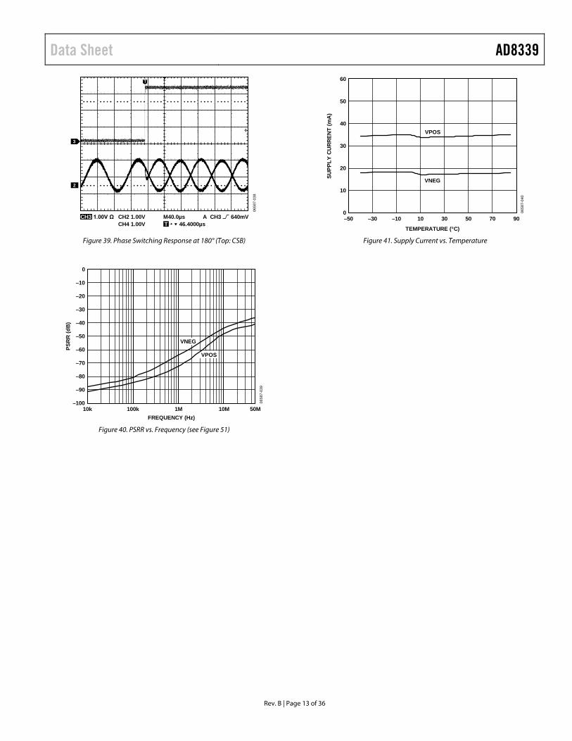
Figure 39. Phase Switching Response at 180° (Top: CSB)
0
–100
–80
10k 100k 50M
0658
7-03
9
FREQUENCY (Hz)
PSR
R (d
B)
–20
–40
–60
–70
–10
–30
–50
–90
1M 10M
VNEG
VPOS
Figure 40. PSRR vs. Frequency (see Figure 51)
60
0
20
–50 90
0658
7-04
0
TEMPERATURE (°C)
SUPP
LY C
UR
REN
T (m
A)
50
40
30
10
–30 –10 10 30 50 70
VPOS
VNEG
Figure 41. Supply Current vs. Temperature
AD8339 Data Sheet
Rev. B | Page 14 of 36
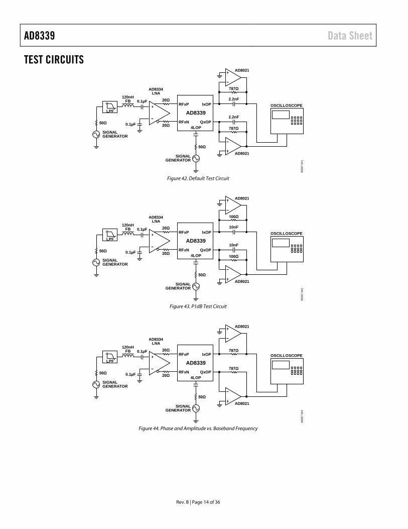
TEST CIRCUITS
0658
7-04
1
50Ω
SIGNALGENERATOR
AD8334LNA
LPFRFxP
RFxN
IxOP
QxOP
AD8339
4LOP50Ω
20Ω
2.2nF
787Ω
2.2nF
787Ω
20Ω
0.1µF120nH
FB
0.1µF
SIGNALGENERATOR
AD8021
AD8021
OSCILLOSCOPE
Figure 42. Default Test Circuit
0658
7-04
2
50Ω
SIGNALGENERATOR
AD8334LNA
LPFRFxP
RFxN
AD8339
4LOP50Ω
20Ω
10nF
100Ω
10nF
100Ω
20Ω
0.1µF120nH
FB
0.1µF
SIGNALGENERATOR
AD8021
AD8021
OSCILLOSCOPEIxOP
QxOP
Figure 43. P1dB Test Circuit
0658
7-04
3
50Ω
SIGNALGENERATOR
AD8334LNA
LPFRFxP
RFxN
AD8339
4LOP50Ω
20Ω
787Ω
787Ω
20Ω
0.1µF120nH
FB
0.1µF
SIGNALGENERATOR
AD8021
AD8021
OSCILLOSCOPEIxOP
QxOP
Figure 44. Phase and Amplitude vs. Baseband Frequency
Data Sheet AD8339
Rev. B | Page 15 of 36
0658
7-04
4
50Ω
SIGNALGENERATOR
SIGNALGENERATOR
AD8334LNA
50Ω
LPFRFxP
RFxN
AD8339
4LOPRSET50Ω
20Ω
787Ω
787Ω
20Ω
0.1µF120nH
FB
0.1µF
SIGNALGENERATOR
AD8021
AD8021
OSCILLOSCOPEIxOP
QxOP
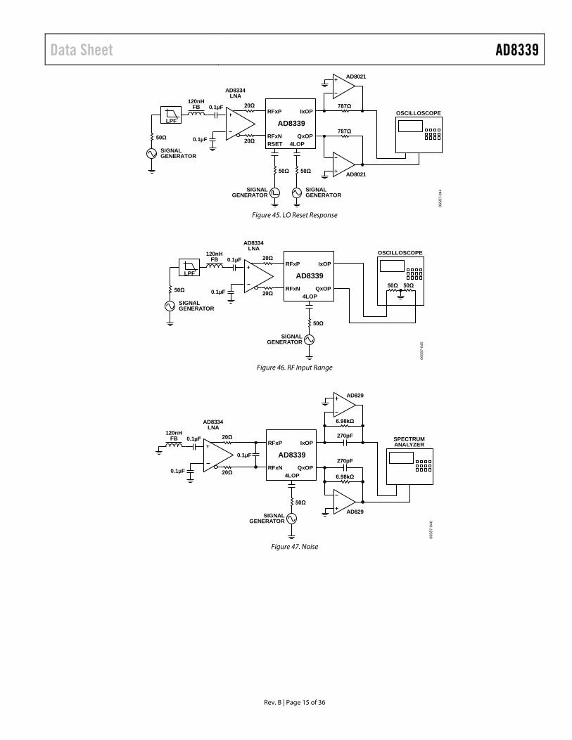
Figure 45. LO Reset Response
0658
7-04
5
50Ω
SIGNALGENERATOR
AD8334LNA
LPFRFxP
RFxN
AD8339
4LOP50Ω
20Ω
50Ω 50Ω20Ω
0.1µF120nH
FB
0.1µF
SIGNALGENERATOR
OSCILLOSCOPE
IxOP
QxOP
Figure 46. RF Input Range
0658
7-04
6
50Ω
SIGNALGENERATOR
AD8334LNA
RFxP
RFxN
AD8339
4LOP
20Ω
270pF0.1µF
6.98kΩ
270pF
6.98kΩ
20Ω
0.1µF120nH
FB
0.1µF
AD829
AD829
SPECTRUMANALYZERIxOP
QxOP
Figure 47. Noise
AD8339 Data Sheet
Rev. B | Page 16 of 36
0658
7-04
7
50Ω
SIGNALGENERATOR
50Ω
SIGNALGENERATOR
50Ω
SIGNALGENERATOR
AD8334LNA
RFxP
RFxN
AD8339
4LOP
20Ω
100pF
787Ω
100pF
787Ω
20Ω
0.1µF120nH
FB
SPLITTER–9.5dB
0.1µF
AD8021
AD8021
SPECTRUMANALYZERIxOP
QxOP
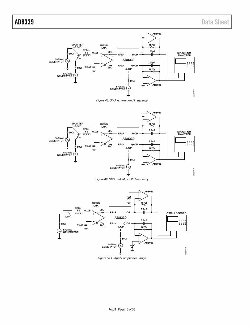
Figure 48. OIP3 vs. Baseband Frequency
0658
7-04
8
50Ω
SIGNALGENERATOR
50Ω
SIGNALGENERATOR
50Ω
SIGNALGENERATOR
AD8334LNA
RFxP
RFxN
AD8339
4LOP
20Ω
2.2nF
787Ω
2.2nF
787Ω
20Ω
0.1µF120nH
FB
SPLITTER–9.5dB
0.1µF
AD8021
AD8021
SPECTRUMANALYZERIxOP
QxOP
Figure 49. OIP3 and IM3 vs. RF Frequency
06
587-
049
50Ω
SIGNALGENERATOR
AD8334LNA
LPFRFxP
RFxN
AD8339
4LOP50Ω
20Ω
2.2nF
787Ω
2.2nF
787Ω
20Ω
0.1µF120nH
FB
0.1µF
SIGNALGENERATOR
AD8021
AD8021
OSCILLOSCOPEIxOP
QxOP
Figure 50. Output Compliance Range
Data Sheet AD8339
Rev. B | Page 17 of 36
0658
7-05
0
SIGNALGENERATOR
RFxP
RFxN
AD8339
4LOP
VPOS
VPOS
VPOS
0.1µF
SPECTRUMANALYZER
SIGNALGENERATOR
IxOP
QxOP
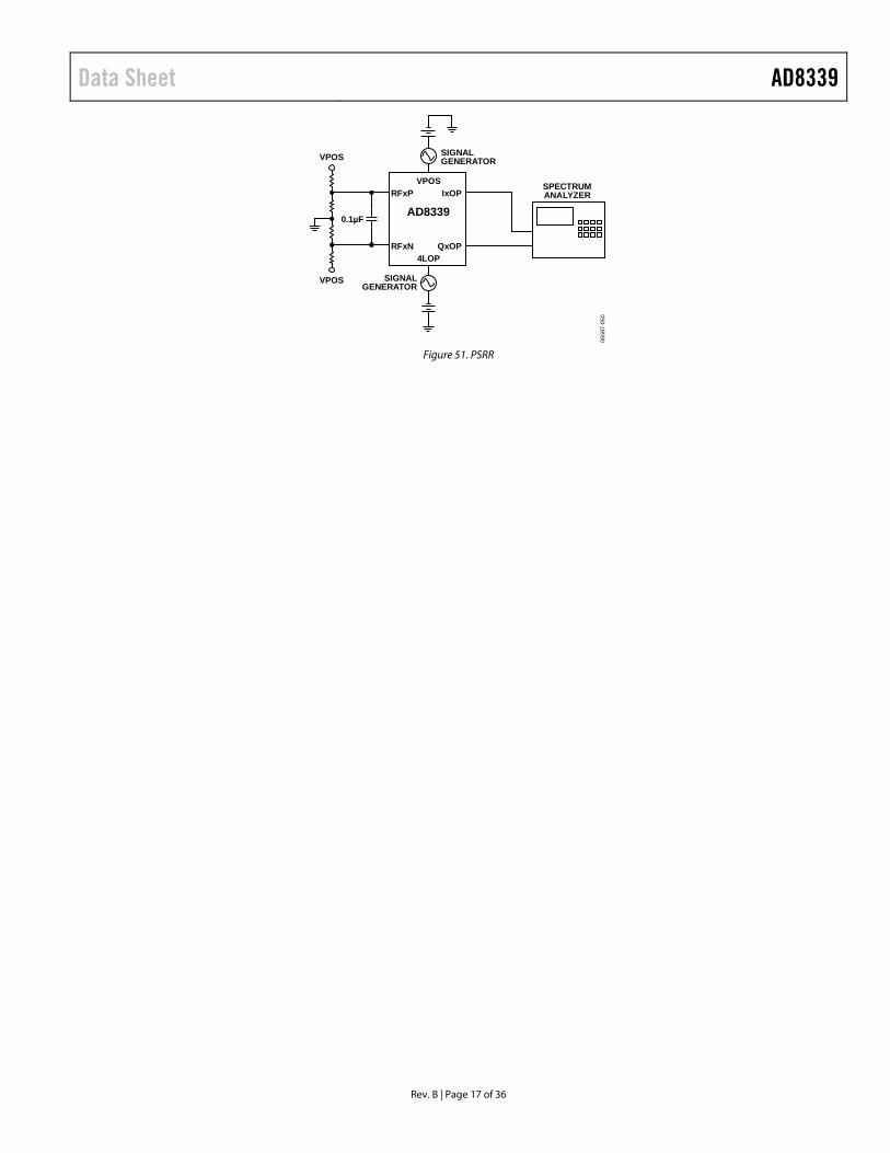
Figure 51. PSRR
AD8339 Data Sheet
Rev. B | Page 18 of 36
THEORY OF OPERATION
0658
7-05
1
COMM 3
COMM 4
VPOS 7
VPOS 8
VPOS28
4LON25
VNEG24
VNEG23
VPOS
11
SDO
12
Q4OP
19
VNEG
20
RF4P
13
RF4N
14
COMM
15
VPOS
16
LODC
17
I4OP
18
RSTS
40
SDI
39
Q1OP
32
VNEG
31
RF1P
38
RF1N
37
COMM
36
VPOS
35
RSET
34
I1OP
33
AD8339
BIAS
SERIALINTERFACE
(SPI)
RF2N 1
RF2P 2
SCLK 5
RF3P 9
RF3N 10 Q3OP21
I3OP22
Q2OP30
I2OP29
VPOS27
4LOP26
CSB 6
CURRENTMIRROR
V TO I
Φ
CURRENTMIRRORΦ
CURRENTMIRROR
V TO I
Φ
CURRENTMIRRORΦ
0°
CURRENTMIRROR
V TO I
Φ
CURRENTMIRRORΦ
CURRENTMIRROR
V TO I
Φ
CURRENTMIRRORΦ
0°
90°LOCAL OSCILLATOR DIVIDE BY 4
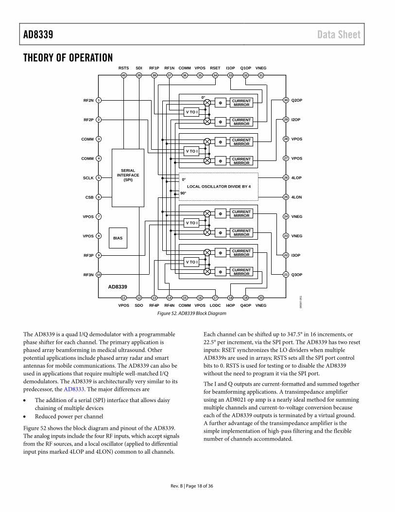
Figure 52. AD8339 Block Diagram
The AD8339 is a quad I/Q demodulator with a programmable phase shifter for each channel. The primary application is phased array beamforming in medical ultrasound. Other potential applications include phased array radar and smart antennas for mobile communications. The AD8339 can also be used in applications that require multiple well-matched I/Q demodulators. The AD8339 is architecturally very similar to its predecessor, the AD8333. The major differences are
• The addition of a serial (SPI) interface that allows daisy chaining of multiple devices
• Reduced power per channel
Figure 52 shows the block diagram and pinout of the AD8339. The analog inputs include the four RF inputs, which accept signals from the RF sources, and a local oscillator (applied to differential input pins marked 4LOP and 4LON) common to all channels.
Each channel can be shifted up to 347.5° in 16 increments, or 22.5° per increment, via the SPI port. The AD8339 has two reset inputs: RSET synchronizes the LO dividers when multiple AD8339s are used in arrays; RSTS sets all the SPI port control bits to 0. RSTS is used for testing or to disable the AD8339 without the need to program it via the SPI port.
The I and Q outputs are current-formatted and summed together for beamforming applications. A transimpedance amplifier using an AD8021 op amp is a nearly ideal method for summing multiple channels and current-to-voltage conversion because each of the AD8339 outputs is terminated by a virtual ground. A further advantage of the transimpedance amplifier is the simple implementation of high-pass filtering and the flexible number of channels accommodated.

Data Sheet AD8339
Rev. B | Page 19 of 36
QUADRATURE GENERATION The internal 0° and 90° LO phases are digitally generated by a divide-by-4 logic circuit. The divider is dc-coupled and inherently broadband; the maximum LO frequency is limited only by its switching speed. The duty cycle of the quadrature LO signals is intrinsically 50% and is unaffected by the asymmetry of the externally connected 4LO input. Furthermore, the divider is implemented such that the 4LO signal reclocks the final flip-flops that generate the internal LO signals and thereby minimizes noise introduced by the divide circuitry.
For optimum performance, the 4LO input is driven differentially, but it can also be driven single-ended. A good choice for a drive is an LVDS device as is done on the AD8339 evaluation board. The common-mode range on each pin is approximately 0.2 V to 3.8 V with the nominal ±5 V supplies.
The minimum 4LO level is frequency dependent when driven by a sine wave. For optimum noise performance, it is important to ensure that the LO source has very low phase noise (jitter) and adequate input level to ensure stable mixer core switching. The gain through the divider determines the LO signal level vs. RF frequency. The AD8339 can be operated at very low frequen-cies at the LO inputs if a square wave is used to drive the LO, as is done with the LVDS driver on the evaluation board.
Beamforming applications require a precise channel-to-channel phase relationship for coherence among multiple channels. A reset pin is provided to synchronize the LO divider circuits in different AD8339s when they are used in arrays. The RSET pin resets the dividers to a known state after power is applied to multiple AD8339s. A logic input must be provided to the RSET pin when using more than one AD8339. Note that at least one channel must be enabled for the LO interface to also be enabled and the LO reset to work. See the Reset Input section for more information.
I/Q DEMODULATOR AND PHASE SHIFTER The I/Q demodulators consist of double-balanced Gilbert cell mixers. The RF input signals are converted into currents by transconductance stages that have a maximum differential input signal capability of 2.8 V p-p. These currents are then presented to the mixers, which convert them to baseband (RF − LO) and twice RF (RF + LO). The signals are phase shifted according to the codes programmed into the SPI latch (see Table 4); the phase bits are labeled PHx0 through PHx3, where 0 indicates LSB and 3 indicates MSB. The phase shift function is an integral part of the overall circuit. The phase shift listed in Column 1 of Table 4 is defined as being between the baseband I or Q channel outputs. As an example, for a common signal applied to a pair of RF inputs to an AD8339, the baseband outputs are in phase for matching phase codes. However, if the phase code for Channel 1 is 0000 and that of Channel 2 is 0001, then Channel 2 leads Channel 1 by 22.5°.
Following the phase shift circuitry, the differential current signal is converted from differential to single-ended via a current mirror. An external transimpedance amplifier is needed to convert the I and Q outputs to voltages.
Table 4. Phase Select Code for Channel-to-Channel Phase Shift Φ Shift PHx3 (MSB) PHx2 PHx1 PHx0 (LSB) 0° 0 0 0 0 22.5° 0 0 0 1 45° 0 0 1 0 67.5° 0 0 1 1 90° 0 1 0 0 112.5° 0 1 0 1 135° 0 1 1 0 157.5° 0 1 1 1 180° 1 0 0 0 202.5° 1 0 0 1 225° 1 0 1 0 247.5° 1 0 1 1 270° 1 1 0 0 292.5° 1 1 0 1 315° 1 1 1 0 337.5° 1 1 1 1
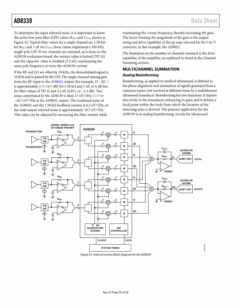
DYNAMIC RANGE AND NOISE Figure 53 is an interconnection block diagram of all four channels of the AD8339. More channels are easily added to the summation (up to 16 when using an AD8021 as the summation amplifier) by wire-OR connecting the outputs as shown for four channels. For optimum system noise performance, the RF input signal is provided by a very low noise amplifier, such as the LNA of the AD8332, AD8334, or AD8335. In beamforming applications, the I and Q outputs of a number of receiver channels are summed (for example, the four channels illustrated in Figure 53). The dynamic range of the system increases by the factor 10 log10(N), where N is the number of channels (assuming random uncorre-lated noise). The noise in the 4-channel example of Figure 53 is increased by 6 dB while the signal quadruples (12 dB), yielding an aggregate SNR improvement of 6 dB (12 − 6).
Judicious selection of the RF amplifier ensures the least degrada-tion in dynamic range. The input referred spectral voltage noise density (en) of the AD8339 is nominally ~11 nV/√Hz. For the noise of the AD8339 to degrade the system noise figure (NF) by 1 dB, the combined noise of the source and the LNA should be approximately twice that of the AD8339, or 22 nV/√Hz. If the noise of the circuitry before the AD8339 is less than 22 nV/√Hz, the system NF degrades more than 1 dB. For example, if the noise contribution of the LNA and source is equal to the AD8339, or 11 nV/√Hz, the degradation is 3 dB. If the circuit noise preceding the AD8339 is 1.3× as large as that of the AD8339 (or ~14 nV/√Hz), the degradation is 2 dB. For a circuit noise 1.45× that of the AD8339 (16 nV/√Hz), the degradation is 1.5 dB.
AD8339 Data Sheet
Rev. B | Page 20 of 36
To determine the input referred noise, it is important to know the active low-pass filter (LPF) values RFILT and CFILT, shown in Figure 53. Typical filter values for a single channel are 1.58 kΩ for RFILT and 1 nF for CFILT; these values implement a 100 kHz single-pole LPF. If two channels are summed, as is done on the AD8339 evaluation board, the resistor value is halved (787 Ω) and the capacitor value is doubled (2.2 nF), maintaining the same pole frequency at twice the AD8339 current.
If the RF and LO are offset by 10 kHz, the demodulated signal is 10 kHz and is passed by the LPF. The single-channel mixing gain from the RF input to the AD8021 output (for example, I1´, Q1´) is approximately 1.7× (4.7 dB) for 1.58 kΩ and 1 nF, or 6 dB less for filter values of 787 Ω and 2.2 nF (0.85× or −1.3 dB). The noise contributed by the AD8339 is then 11 nV/√Hz × 1.7 or ~18.7 nV/√Hz at the AD8021 output. The combined noise of the AD8021 and the 1.58 kΩ feedback resistor is 6.3 nV/√Hz, so the total output referred noise is approximately 19.7 nV/√Hz. This value can be adjusted by increasing the filter resistor while
maintaining the corner frequency, thereby increasing the gain. The factor limiting the magnitude of the gain is the output swing and drive capability of the op amp selected for the I-to-V converter, in this example, the AD8021.
The limitation on the number of channels summed is the drive capability of the amplifier, as explained in detail in the Channel Summing section.
MULTICHANNEL SUMMATION Analog Beamforming
Beamforming, as applied to medical ultrasound, is defined as the phase alignment and summation of signals generated from a common source, but received at different times by a multielement ultrasound transducer. Beamforming has two functions: it imparts directivity to the transducer, enhancing its gain, and it defines a focal point within the body from which the location of the returning echo is derived. The primary application for the AD8339 is in analog beamforming circuits for ultrasound.
0658
7-05
2
AD8339AD8332, AD8334 LNAOR AD8335 PREAMP
TRANSMITTER
TRANSDUCER
CLOCK DATA
T/RSW
RFB
2
2
2
2
2
Φ
Φ
I1
Q1
T/RSW
RFB
2
2
2
2
2
Φ
Φ
I2
Q2
T/RSW
RFB
2
2
2
2
2
Φ
Φ
I3
Q3
T/RSW
RFB
2
2
2
2
2
Φ
Φ
I4
Q4
SDICONTROLLER
QUADRATUREDIVIDER
0° 90°
SYSTEM TIMING
CFILT
RFILT ΣQ
AD7665 ORAD7686
AD7665 ORAD7686
16-BIT ADC Q DATA
CFILT
RFILT ΣI
AD8021
AD8021
16-BIT ADC I DATA
Figure 53. Interconnection Block Diagram for the AD8339

Data Sheet AD8339
Rev. B | Page 21 of 36
Combining Phase Compensation and Analog Beamforming
Modern ultrasound machines used for medical applications employ an array of receivers for beamforming, with typical CW Doppler array sizes of up to 64 receiver channels that are phase shifted and summed together to extract coherent information. When used in multiples, the desired signals from each of the channels can be summed to yield a larger signal (increased by a factor N, where N is the number of channels), and the noise is increased by the square root of the number of channels. This technique enhances the signal-to-noise performance of the machine. The critical elements in a beamformer design are the means to align the incoming signals in the time domain and the means to sum the individual signals into a composite whole.
In traditional analog beamformers incorporating Doppler, a V-to-I converter per channel and a crosspoint switch precede passive delay lines used as a combined phase shifter and summing circuit. The system operates at the carrier frequency (RF) through the delay line, which also sums the signals from the various channels, and then the combined signal is down-converted by a very large dynamic range I/Q demodulator.
The resultant I and Q signals are filtered and then sampled by two high resolution analog-to-digital converters. The sampled signals are processed to extract the relevant Doppler information.
Alternatively, the RF signal can be processed by downconversion on each channel individually, phase shifting the downconverted signal, and then combining all channels. The AD8333 and the AD8339 implement this architecture. The downconversion is done by an I/Q demodulator on each channel, and the summed current output is the same as in the delay line approach. The subsequent filters after the I-to-V conversion and the ADCs are similar.
The AD8339 integrates the phase shifter, frequency conversion, and I/Q demodulation into a single package and directly yields the baseband signal. Figure 54 is a simplified diagram showing the concept for all four channels. The ultrasound wave (US wave) is received by four transducer elements, TE1 through TE4, in an ultrasound probe and generates signals E1 through E4. In this example, the phase at TE1 leads the phase at TE2 by 45°.
Channel Summing
Figure 55 shows a 16-channel beamformer using AD8339s, AD8021s, and an AD797. The number of channels summed is limited by the current drive capability of the amplifier used to implement the active low-pass filter and current-to-voltage converter. An AD8021 sums up to 16 AD8339 outputs.
In an ultrasound application, the instantaneous phase difference between echo signals is influenced by the transducer-element spacing, the wavelength (λ), the speed of sound in the media, the angle of incidence of the probe to the target, and other factors. In Figure 54, the signals E1 through E4 are amplified 19 dB by the low noise amplifiers in the AD8334; for lower power portable ultrasound applications, the AD8335 can be used instead of the AD8334 for the lowest power per channel. For optimum signal-to-noise performance, the output of the LNA is applied directly to the input of the AD8339. To sum the signals E1 through E4, E2 is shifted 45° relative to E1 by setting the phase code in Channel 2 to 0010, E3 is shifted 90° (0100), and E4 is shifted 135° (0110). The phase aligned current signals at the output of the AD8339 are summed in an I-to-V converter to provide the combined output signal with a theoretical improvement in dynamic range of 6 dB for the four channels.
06
587-
053
TRANSDUCERELEMENTS TE1THROUGH TE4
CONVERT US TOELECTRICAL
SIGNALS AD8334
AD8339PHASE BITSETTINGS
CH 1PHASE SET
FOR 135°LAG
S1 THROUGH S4ARE NOW IN
PHASE
SUMMEDOUTPUT
S1 + S2 + S3 + S4
E1
CH 2PHASE SET
FOR 90°LAG
19dBLNA
E2
CH 3PHASE SET
FOR 45°LAG
CH 4PHASE SET
FOR 0°LAG
19dBLNA
E319dBLNA
E4
S1
S2
S3
S419dBLNA
4 US WAVESARE DELAYED45° EACH WITHRESPECT TOEACH OTHER
90°
45°
135°
0°
Figure 54. Simplified Example of the AD8339 Phase Shifter

AD8339 Data Sheet
Rev. B | Page 22 of 36
C21µF
R1100Ω
C118nF
R2698Ω
R3698Ω
3AD8021+
–2
C35.6nF
UP TO 16 AD8339 I OR QOUTPUTS AT 3.1mA PEAK
EACH WHEN PHASE SHIFT ISSET FOR 45°
R4
3AD797+
2
0.1µF+5V
0.1µF
+10V
–5V
0.1µF0.1µF
–10V
LPF188kHz
HPF1100Hz
LPF281kHz
∑ ∑
FIRST ORDERSUMMING
AMPLIFIER(S)
SECOND ORDERSUMMING AMPLIFIER
+2.8V BASEBANDSIGNAL
–
FROM OTHERAD8021
SUMMING AMPLIFIERS
0658
7-15
5
Figure 55. 16-Channel Beamformer Using the AD8339
Data Sheet AD8339
Rev. B | Page 23 of 36
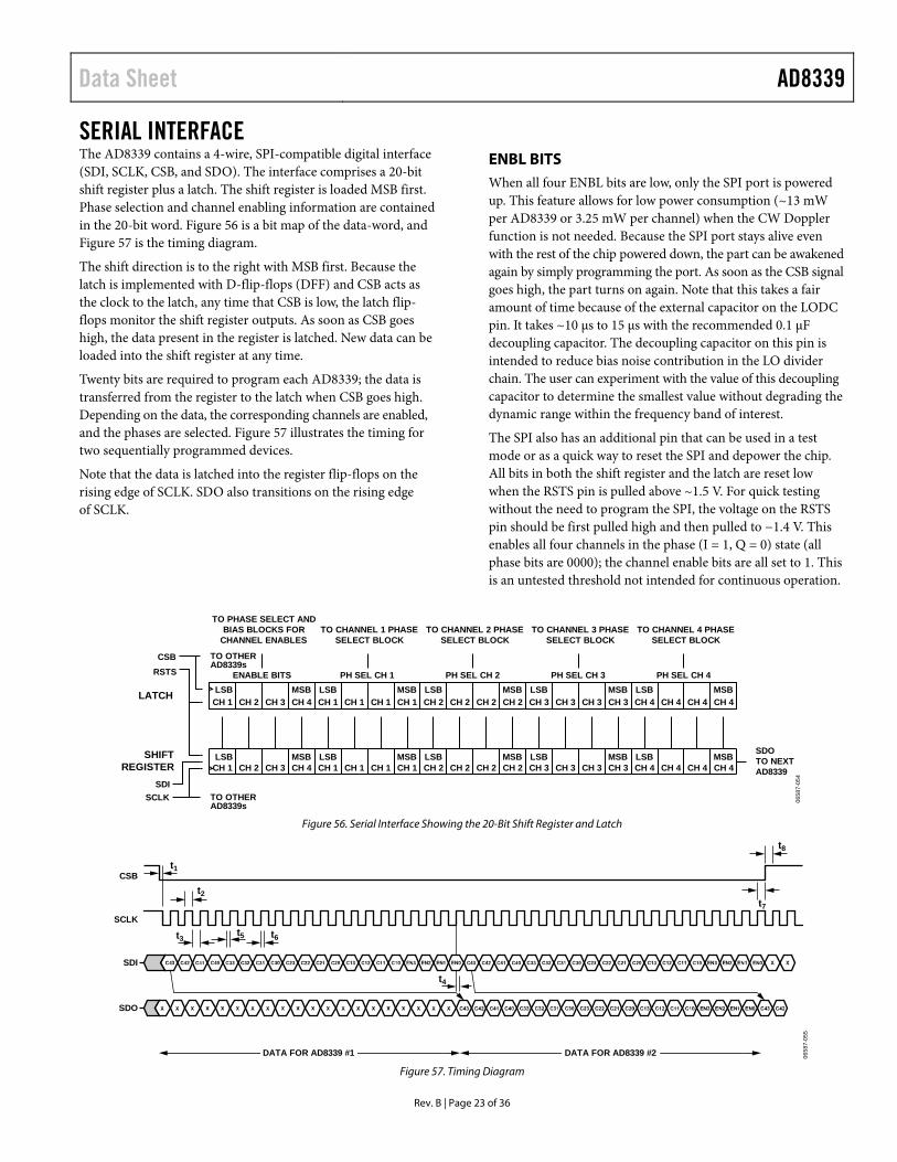
SERIAL INTERFACE The AD8339 contains a 4-wire, SPI-compatible digital interface (SDI, SCLK, CSB, and SDO). The interface comprises a 20-bit shift register plus a latch. The shift register is loaded MSB first. Phase selection and channel enabling information are contained in the 20-bit word. Figure 56 is a bit map of the data-word, and Figure 57 is the timing diagram.
The shift direction is to the right with MSB first. Because the latch is implemented with D-flip-flops (DFF) and CSB acts as the clock to the latch, any time that CSB is low, the latch flip-flops monitor the shift register outputs. As soon as CSB goes high, the data present in the register is latched. New data can be loaded into the shift register at any time.
Twenty bits are required to program each AD8339; the data is transferred from the register to the latch when CSB goes high. Depending on the data, the corresponding channels are enabled, and the phases are selected. Figure 57 illustrates the timing for two sequentially programmed devices.
Note that the data is latched into the register flip-flops on the rising edge of SCLK. SDO also transitions on the rising edge of SCLK.
ENBL BITS When all four ENBL bits are low, only the SPI port is powered up. This feature allows for low power consumption (~13 mW per AD8339 or 3.25 mW per channel) when the CW Doppler function is not needed. Because the SPI port stays alive even with the rest of the chip powered down, the part can be awakened again by simply programming the port. As soon as the CSB signal goes high, the part turns on again. Note that this takes a fair amount of time because of the external capacitor on the LODC pin. It takes ~10 μs to 15 μs with the recommended 0.1 μF decoupling capacitor. The decoupling capacitor on this pin is intended to reduce bias noise contribution in the LO divider chain. The user can experiment with the value of this decoupling capacitor to determine the smallest value without degrading the dynamic range within the frequency band of interest.
The SPI also has an additional pin that can be used in a test mode or as a quick way to reset the SPI and depower the chip. All bits in both the shift register and the latch are reset low when the RSTS pin is pulled above ~1.5 V. For quick testing without the need to program the SPI, the voltage on the RSTS pin should be first pulled high and then pulled to −1.4 V. This enables all four channels in the phase (I = 1, Q = 0) state (all phase bits are 0000); the channel enable bits are all set to 1. This is an untested threshold not intended for continuous operation.
0658
7-05
4
TO PHASE SELECT ANDBIAS BLOCKS FOR
CHANNEL ENABLESTO CHANNEL 1 PHASE
SELECT BLOCKTO CHANNEL 2 PHASE
SELECT BLOCKTO CHANNEL 3 PHASE
SELECT BLOCKTO CHANNEL 4 PHASE
SELECT BLOCK
SHIFTREGISTER
LATCH
SCLKSDI
CH 1 CH 3 CH 4 CH 3 CH 3CH 3 CH 3 CH 4 CH 4CH 4CH 4CH 1 CH 1 CH 1 CH 1 CH 2 CH 2 CH 2 CH 2CH 2
CH 1 CH 3 CH 4 CH 3 CH 3CH 3 CH 3 CH 4 CH 4CH 4CH 4CH 1 CH 1 CH 1 CH 1 CH 2 CH 2 CH 2 CH 2CH 2
MSBLSB MSBLSB MSBLSB MSBLSB MSBLSB
MSBLSB MSBLSB MSBLSB MSBLSB MSBLSB
SDOTO NEXTAD8339
ENABLE BITS PH SEL CH 1 PH SEL CH 2 PH SEL CH 3 PH SEL CH 4RSTSCSB TO OTHER
AD8339s
TO OTHERAD8339s
Figure 56. Serial Interface Showing the 20-Bit Shift Register and Latch
0658
7-05
5
CSBt1
t2t7
t8
t3
t4
t5 t6
SCLK
SDI
SDO
DATA FOR AD8339 #1 DATA FOR AD8339 #2 Figure 57. Timing Diagram
AD8339 Data Sheet
Rev. B | Page 24 of 36
APPLICATIONS INFORMATION The AD8339 is the key component of a phase shifter system that aligns time-skewed information contained in RF signals. Combined with a variable gain amplifier (VGA) and a low noise amplifier (LNA) as in the AD8332/AD8334/AD8335 VGA family, the AD8339 forms a complete analog receiver for a high performance ultrasound CW Doppler system.
LOGIC INPUTS AND INTERFACES The SDI, SCLK, SDO, CSB, and RSET pins are CMOS com-patible to 1.8 V. The threshold of the RSTS pin is 1.5 V with a hysteresis of ±0.3 V. Each logic input pin is Schmitt trigger activated, with a threshold centered at ~1.3 V and a hysteresis of ±0.1 V around this value.
The only logic output, SDO, generates a signal that has a logic low level of ~0.2 V and a logic high level of ~1.9 V to allow for easy interfacing to the next AD8339 SDI input. Note that the capacitive loading for the SDO pin should be kept as small as possible (<5 pF), ideally only a short trace to the SDI pin of the next chip. The output slew is limited to approximately ±500 μA, which limits the speed when a large capacitor is connected. Excessive values of parasitic capacitance on the SDO pin can affect the timing and loading of data into the SDI input of the next chip.
RESET INPUT The RSET pin is used to synchronize the LO dividers in AD8339 arrays. Because they are driven by the same internal LO, the four channels in any AD8339 are inherently synchronous. However, when multiple AD8339s are used, it is possible that their dividers wake up in different phase states. The function of the RSET pin is to phase align all the LO signals in multiple AD8339s.
The 4LO divider of each AD8339 can be initiated in one of four possible states: 0°, 90°, 180°, or 270° relative to other AD8339s. The internally generated I/Q signals of each AD8339 LO are always at a 90° angle relative to each other, but a phase shift can occur during power-up between the dividers of multiple AD8339s used in a common array.
The LO divider reset function has been improved in the AD8339 compared with the AD8333. The RSET pin still provides an asynchronous reset of the LO dividers by forcing the internal LO to hang; however, in the AD8339, the LO reset function is fast and does not require a shutdown of the 4LO input signal.
The RSET mechanism also allows the measurement of non-mixing gain from the RF input to the output. The rising edge of the active high RSET pulse can occur at any time; however, the duration should be ≥20 ns minimum. When the RSET pulse transitions from high to low, the LO dividers are reactivated on the next rising edge of the 4LO clock. To guarantee synchronous operation of an array of AD8339s, the RSET pulse must go low on all devices before the next rising edge of the 4LO clock. Therefore, it is best to have the RSET pulse go low on the falling edge of the 4LO clock; at the very least, the tSETUP should be ≥5 ns. An optimal timing setup is for the RSET pulse to go high on a 4LO falling edge and to go low on a 4LO falling edge; this gives 10 ns of setup time even at a 4LO frequency of 50 MHz (12.5 MHz internal LO).
Check the synchronization of multiple AD8339s using the following procedure:
1. Activate at least one channel per AD8339 by setting the appropriate channel enable bit in the serial interface.
2. Set the phase code of all AD8339 channels to the same logic state, for example, 0000.
3. Apply the same test signal to all devices to generate a sine wave in the baseband output and measure the output of one channel per device.
4. Apply an RSET pulse to all AD8339s. 5. Because all the phase codes of the AD8339s should be the
same, the combined signal of multiple devices should be N times greater than a single channel. If the combined signal is less than N times one channel, one or more of the LO phases of the individual AD8339s is in error.
LO INPUT The LO input is a high speed, fully differential analog input that responds to differences in the input levels (and not logic levels). The LO inputs can be driven with a low common-mode voltage amplifier, such as the National Semiconductor® DS90C401 LVDS driver. The graph in Figure 22 shows the range of common-mode voltages. Logic families such as TTL or CMOS are unsuitable for direct coupling to the LO input.

Data Sheet AD8339
Rev. B | Page 25 of 36
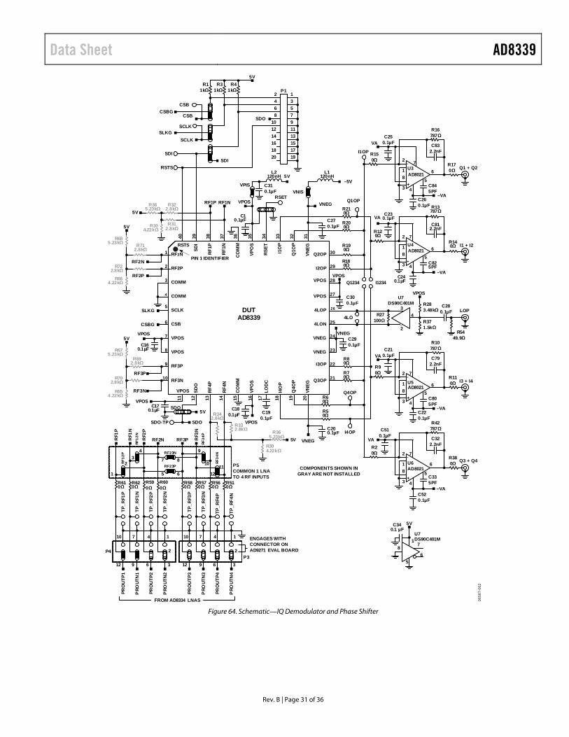
EVALUATION BOARD Figure 58 is a photograph of the AD8339 evaluation board; the schematic diagrams are shown in Figure 63, Figure 64, and Figure 65. Four single-ended RF inputs can be phase aligned using the LNA inputs of an AD8334 and the 16 phase adjust-ment options of the AD8339. The RF input signals can be derived from three sources, user selectable by jumpers. Test points enable signal tracing at various circuit nodes.
The AD8339-EVALZ requires bipolar 5 V power supplies. A 3.3 V on-board regulator provides power for the USB and EEPROM devices. The AD8339 is configured using the software provided on the CD included with the evaluation board, or using an external digital pattern generator via the 20-pin flat-cable connector P1.
0658
7-15
7
Figure 58. AD8339 Evaluation Board
AD8339 Data Sheet
Rev. B | Page 26 of 36
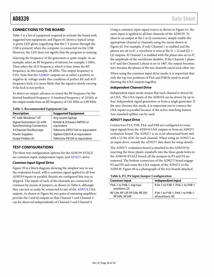
CONNECTIONS TO THE BOARD Table 5 is a list of equipment required to activate the board with suggested test equipment, and Figure 61 shows a typical setup. A green LED glows (signifying that the 5 V power through the USB is present) when the computer is connected via the USB. However, the LED does not signify that the program is running.
Selecting the frequency of the generators is quite simple. As an example, select an RF frequency of interest, for example, 5 MHz. Then select the 4LO frequency, which is four times the RF frequency, in this example, 20 MHz. The output frequency is 0 Hz. Note that the AD8021 outputs are at either a positive or negative dc voltage under this condition of perfect RF and 4LO frequency lock; it is more likely that the signal is slowly varying if the lock is not perfect.
To detect an output, advance or retard the RF frequency by the desired baseband frequency. A baseband frequency of 10 kHz at the output results from an RF frequency of 5.01 MHz or 4.99 MHz.
Table 5. Recommended Equipment List Description Suggested Equipment PC with Windows® XP Any recent laptop Signal Generators (2) with Synchronizing Connectors
Rohde & Schwarz SMT03 or equivalent
4-Channel Oscilloscope Tektronix DPO7104 or equivalent Power Supplies Agilent E3631A or equivalent Scope Probes (4) Tektronix P6104 or equivalent
TEST CONFIGURATIONS The three test configuration options for the AD8339-EVALZ are common input, independent input, and AD9271 drive.
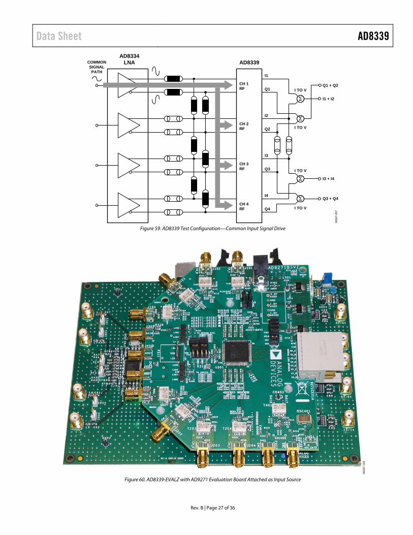
Common Input Signal Drive
Figure 59 is a block diagram showing the simplest way to use the evaluation board, with a common signal applied to all four AD8339 inputs in parallel. Boards are configured this way as shipped. The inputs of each of the channels are connected in common by means of jumpers, as shown in Table 6, although they can just as easily be connected to any of the AD8334 LNA outputs. As shown in Figure 64, two pairs of summing amplifiers provide the I and Q outputs so that Channel 1 and Channel 2 can be observed independently of Channel 3 and Channel 4.
Using a common input signal source as shown in Figure 61, the same input is applied to all four channels of the AD8339. To observe an output at the I or Q connectors, simply enable the appropriate channel or channels using the menu shown in Figure 62. For example, if only Channel 1 is enabled and the phases are set to 0°, a waveform is seen at the I1 + I2 and Q1 + Q2 outputs. If Channel 2 is enabled with the phase also set to 0°, the amplitude of the waveforms doubles. If the Channel 1 phase is 0° and the Channel 2 phase is set to 180°, the output becomes zero, because the phases of the two channels cancel each other out.
When using the common input drive mode, it is important that only the top two positions of P4A and P4B be used to avoid shorting the LNA outputs together.
Independent Channel Drive
Independent input mode means that each channel is driven by an LNA. The LNA inputs of the AD8334 can be driven by up to four independent signal generators or from a single generator. If the user chooses this mode, it is important not to connect the LNA inputs in parallel because of the active matching feature. Any standard splitter can be used.
AD9271 Input Drive
Connectors P3A, P3B, P4A, and P4B are configured to route input signals from the AD8334 LNA outputs or from an AD9271 evaluation board. The AD9271 is an octal ultrasound front end with a 12-bit ADC for each channel. When using an AD9271 as an input drive, consult the AD9271 data sheet for setup details.
The AD9271 evaluation board is attached to the AD8339 by inserting the three plastic standoffs into the three guide holes in the AD8339-EVALZ board; all the jumpers in P3 and P4 are removed. The bottom connectors of the AD9271 board engage P3 and P4 and route the LNA outputs of the AD9271 to the AD8339. Figure 60 is a photograph of the two boards attached.
Table 6. P3, P4 Input Jumper Configuration Common Input Independent Input P4A-1 to P4B-1, top two
positions (2) P3A-1 to P3B-1, P4A-1 to P4B-1
RF12N, RF12P, RF23N, RF23P, RF34N, RF34P
P3A-1 to P3B-1, P4A-1 to P4B-1, all positions (8)
Data Sheet AD8339
Rev. B | Page 27 of 36
0658
7-05
7
AD8334LNA AD8339COMMON
SIGNALPATH
CH 1RF
CH 2RF
CH 3RF
CH 4RF
I1
I1 + I2
Q1Q1 + Q2
Q3 + Q4
I3 + I4
I2
Q2
I3
Q3
I4
Q4 I TO V
I TO V
I TO V
I TO V
Figure 59. AD8339 Test Configuration—Common Input Signal Drive
0658
7-15
9
Figure 60. AD8339-EVALZ with AD9271 Evaluation Board Attached as Input Source

AD8339 Data Sheet
Rev. B | Page 28 of 36
0658
7-05
9
TOP:SIGNAL GENERATOR FOR 4LO INPUT (FOR EXAMPLE, 20MHz, 1Vp-p)BOTTOM:SIGNAL GENERATOR FOR RF INPUT (FOR EXAMPLE, 5.01MHz)
SYNCHRONIZEGENERATORS
USBCABLE
PERSONALCOMPUTER
POWER SUPPLY
+5V–5V
4LOINPUT
OUTPUTS
Figure 61. AD8339-EVALZ Typical Test Setup
Data Sheet AD8339
Rev. B | Page 29 of 36
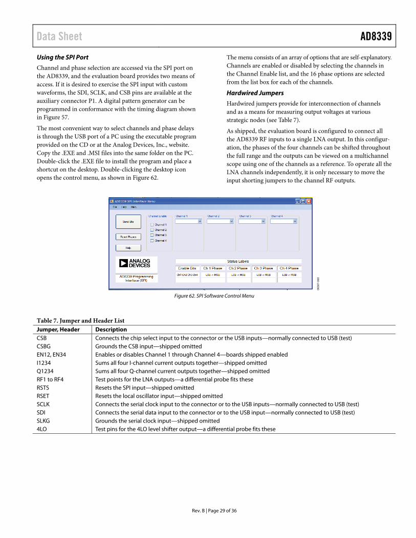
Using the SPI Port
Channel and phase selection are accessed via the SPI port on the AD8339, and the evaluation board provides two means of access. If it is desired to exercise the SPI input with custom waveforms, the SDI, SCLK, and CSB pins are available at the auxiliary connector P1. A digital pattern generator can be programmed in conformance with the timing diagram shown in Figure 57.
The most convenient way to select channels and phase delays is through the USB port of a PC using the executable program provided on the CD or at the Analog Devices, Inc., website. Copy the .EXE and .MSI files into the same folder on the PC. Double-click the .EXE file to install the program and place a shortcut on the desktop. Double-clicking the desktop icon opens the control menu, as shown in Figure 62.
The menu consists of an array of options that are self-explanatory. Channels are enabled or disabled by selecting the channels in the Channel Enable list, and the 16 phase options are selected from the list box for each of the channels.
Hardwired Jumpers
Hardwired jumpers provide for interconnection of channels and as a means for measuring output voltages at various strategic nodes (see Table 7).
As shipped, the evaluation board is configured to connect all the AD8339 RF inputs to a single LNA output. In this configur-ation, the phases of the four channels can be shifted throughout the full range and the outputs can be viewed on a multichannel scope using one of the channels as a reference. To operate all the LNA channels independently, it is only necessary to move the input shorting jumpers to the channel RF outputs.
0658
7-06
0
Figure 62. SPI Software Control Menu
Table 7. Jumper and Header List Jumper, Header Description CSB Connects the chip select input to the connector or the USB inputs—normally connected to USB (test) CSBG Grounds the CSB input—shipped omitted EN12, EN34 Enables or disables Channel 1 through Channel 4—boards shipped enabled I1234 Sums all four I-channel current outputs together—shipped omitted Q1234 Sums all four Q-channel current outputs together—shipped omitted RF1 to RF4 Test points for the LNA outputs—a differential probe fits these RSTS Resets the SPI input—shipped omitted RSET Resets the local oscillator input—shipped omitted SCLK Connects the serial clock input to the connector or to the USB inputs—normally connected to USB (test) SDI Connects the serial data input to the connector or to the USB input—normally connected to USB (test) SLKG Grounds the serial clock input—shipped omitted 4LO Test pins for the 4LO level shifter output—a differential probe fits these
AD8339 Data Sheet
Rev. B | Page 30 of 36
0658
7-06
1
INH2
LMD2
COM2X
LON2
LOP2
VIP2
VIN2
VPS2
CO
M3
CO
M4
INH
4
L MD
4
CO
M4X
LON
4
LOP
4
VIP
4
COM2
CO
M1
INH
1
LMD
1
CO
M1X
LON
1
LOP1
VIP1
COM12
VOH1
VOL1
VPS12
VOL2
VOH2
COM12
MODEU1AD8334
PIN 1IDENTIFIER
VPS3 NC
VIN3 COM34
VIN
4
VPS4
VIN
1
VPS1
VIP3
LOP3
LON3
COM3X
LMD3
INH3
GA
IN12
CLM
P12
EN12
EN34
VCM
1 VCM2
VOH3
VOL3
VPS34
VOL4
VOH4
COM34
GA
IN34
CLM
P34
HIL
O
VCM
4
VCM
3
NC
IN1
LOP4
C822pF
CFB218nF
RFB2274Ω
C430.1µF
R4420Ω
R4320Ω
C440.1µF
C622pF
CFB118nF
C680.1µF
RFB1274Ω
CFB418nF
RFB4274Ω
C550.1µF
R4620Ω
R4520Ω
C450.1µF
L9120nH
L8120nH
CFB318nF
RFB3274Ω
C1022pF
C1222pF
IN2
IN3 IN4
C500.1µF
C630.1µF
C560.1µF
C570.1µF
1
2
3
4
5
6
7
8
9
10
11
12
13
14
15
16
5V
R4720Ω
R4820Ω
5V
5V
5VC640.1µF
C650.1µF
C590.1µF
C580.1µF
C490.1µF
17 323130292827262524232221201918
C670.1µF
L10120nH
C600.1µF
L7120nH
C660.1µFC54
0.1µF
C530.1µF
49505152535455565758596061626364
LOP2
L15120nH
5V
L14120nH
C850.1µF
L17120nH
C870.1µF
C880.1µF
C460.1µF
C470.1µF
C480.1µF
C610.1µF
C620.1µF
LOP1 LON1
R4920Ω
R5020Ω
C860.1µF
L13120nH
LON4
IN4S
IN3S
IN1S
IN2S
48
47NC
46NC
45
44NC
43NC
42
41
40
39
38NC
37
36
35NC
34NC
33
LON2
L16120nH
LOP3
LON3
R640Ω
L12120nH
R630Ω
5V
EN12 EN34EN
DISDIS
EN
RF1
RF4
RF3
RF2
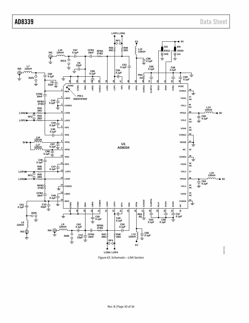
Figure 63. Schematic—LNA Section
Data Sheet AD8339
Rev. B | Page 31 of 36
0658
7-06
2
5V
RF1P RF1N
–5V
RF2N
RF2P
COMM
COMM
SCLK
CSB
VPOS
VPOS
VPOS SDO
RF4
P
RF4
N
CO
MM
VPO
S
LOD
C
I4O
P
RSTS
SDI
RF1
P
RF1
N
CO
MM
VPO
S
RSE
T
I1O
P
Q2OP
I2OP
VPOS
VPOS
4LOP
4LON
VNEG
VNEG
DUTAD8339
PIN 1 IDENTIFIER
RF3P I3OP
RF3N Q3OP
Q4O
P
VNEG
Q1O
P
VNEG
U7DS90C401M
I1 + I2
C10.1µF
RSET
19
123
67
10
45
89
17
1114
151820
1613
12
5VR1
1kΩ
R180Ω
R190Ω
R210Ω
R200Ω
R70Ω
R80Ω
VNEG
R50Ω
R60Ω
Q3 + Q4
Q1 + Q2
I3 + I4
L1120nH
R371.5kΩ
C300.1µF
R27100Ω
R283.48kΩ
R5449.9Ω
C280.1µF
C250.1µF
R16787Ω
VA
C260.1µF
–VA
–VA
–VA
–VA
C845PF
C832.2nF
R170Ω
2 718
3 4
5
6AD8021
+
-
R150Ω
C230.1µF
R13787Ω
VA
C240.1µF
C825PF
C812.2nF
R140Ω
2 7
18
3 4
5
6AD8021
+
-
R120Ω
C210.1µF
R10787Ω
VA
C220.1µF
C805PF
C792.2nF
R110Ω
2 7
18
3 4
5
6AD8021
+
-
R90Ω
C510.1µF
R42787Ω
VA
C520.1µF
C335PF
C322.2nF
R380Ω
2 7
18
3 4
5
6U6
U5
U4
U3
AD8021
+
-
R20Ω
LOP
L2120nH
VPOS
VPOS
VPOS
VPOS
VPOS
5V C180.1µF
C170.1µF
VPOS
C160.1µF
VNEG
VNEG
C270.1µF
R332.8kΩ
SDI
SCLK
CSB
SCLK
5
17
68
5VC340.1 µF
2
34
U7DS90C401M
SDO
SDO
2
3
4
5
6
8
9
10
7
R560Ω
C190.1µF
CSB
SDI
SDO-TP
RSTS
40 3839 37 36 35
VPIS
34 33 32 31
30
29
28
27
26
25
24
23
22
21
11 12 13 14 15 16 17
5VR36
5.23kΩ
R304.22kΩ
R342.8kΩ
RF3P RF3
N
RF2
P
RF2NRF1
P
RF1
N
CSBG
RF2N
RF2P
RF3N
RF3P
SLKG
CSBG
SLKG
R31kΩ
R41kΩ P1
5V
R675.23kΩ
R654.22kΩ
5VR36
5.23kΩ
R304.22kΩ
R322.8kΩ
R312.8kΩ
R692.8kΩ
R702.8kΩ
5V
R685.23kΩ
R664.22kΩ
R712.8kΩ
R722.8kΩ
1
ENGAGES WITHCONNECTOR ONAD9271 EVAL BOARD
R510Ω
R610Ω
R620Ω
R570Ω
R580Ω
R590Ω
R600Ω
4LO
I4OP
Q4OP
I1OP
Q1OP
I1234Q1234
SDO
C310.1µF VNIS
C290.1µF
2
1
2
PRO
UTP
3
PRO
UTN
3
PRO
UTP
4
PRO
UTN
4
PRO
UTP
1
PRO
UTN
1
PRO
UTP
2
PRO
UTN
2
FROM AD8334 LNAS
6
7 4
3
10
912 6 3912
17 410
P4P3
C200.1µF
RF12
P RF23N
RF23P
RF12
N
RF34
P
RF34
N
P5COMMON 1 LNATO 4 RF INPUTS1
23
4
5 6
7 8
9
1011
12
TP_R
F1P
TP_R
F1N
TP_R
F2P
T P_R
F2N
TP_R
F3P
TP_R
F3N
TP_R
F 4P
TP_R
F4N
COMPONENTS SHOWN INGRAY ARE NOT INSTALLED
18 19 20
Figure 64. Schematic—IQ Demodulator and Phase Shifter

AD8339 Data Sheet
Rev. B | Page 32 of 36
0658
7-06
3
PA5/FIFOADR1
PA4/FIFOADR0
GND
PA7/FLAGD/SLCS
PA3/WU2
CTL1/FLAGB
PA0/INT0#
XTALOUT
RDY0/SLRD
VCC
CTL2/FLAGC
CTL0/FLAGA
PA6/PKTEND
RESET#
25 26 2717 18 19 21 22 23 2415 16
8
7
6
5
1
4
3
2
14
13
9
12
11
10
50 4956 55 5154 53 52
35
36
37
38
42
39
40
41
34
33
30
31
32
48 47 4346 45 44
DPLUS
AGND
XTALIN
DMINUS
IFCLK/PE0/TOUT
GND
RESERVED
AVCC
SCL
SDA
PB0/
FD0
VCC
GN
D
VCC
GN
D
PB2/
FD2
PB6/
FD6
PB4/
FD4
PB5/
FD5
PB3/
FD3
PB1/
FD1
PA1/INT1#
PA2/SLOE
VCC
GN
D
PD7/
FD15
PD5/
FD13
CLK
OU
T/PE
1/T1
OU
T
PD4/
FD12
GN
D
PD6/
FD14
20
U2CY7C68013A-56LFXC
A0
NC
C312 pF
A1A2
C720.1µF
C740.1µF
C730.1µF
C422pF
SCLK (SHT2)
Y124MHz
A7USB
TYPE B
VSS
CSB (SHT2)
28
29
SDI (SHT2)PB
7/FD
7
RDY1/SLWR
VCC
AVCC
PD2/
FD10
PD3/
FD11
WA
KEU
P
PD1/
FD9
PD0/
FD8
VCC
AGND
R3910kΩ
3.3V
3.3V
3.3V
3.3V
3.3V
3.3V
3.3V
3.3V
NC NC NC
NC
NC
NC
NC
NC
NC
NC
NC
NC
NC
NC
NC
NC
NC
NC
NC
NC
NC
NC NC NC NC NC NC
1
23
4R55
499Ω
C212pF
8
7
5
1
4
3
2
6
3.3V
3.3V
VCCWP
SCLSDA
R5222.1kΩ
R5322.1kΩ
C750.1µF
C522pF
C70.1 µF
C91µF10V
C770.1µF
OUT
ADP3339AKCZ-3.3
L11120nH
IN
OUT
GND3 12
TAB
+
Z124LC00/P
5VVBUSD–
D+
GND
C700.1µF
C690.1µF
CR1
5V
C760.1µF
R40100kΩ
R41100kΩ
C710.1µF
W3
VA
+
–VA
+
5V
C1410µF25V
C780.1µF
C1310µF25V
C1110µF25V
C1510µF25V
5VS
3.3V
–5VS
+
–5V
C380.1µF
C370.1µF
C360.1µF
C350.1µF
+
VAS –VAS
P2
L6120nH
L5120nH
L4120nH
L3120nH
RED ORGGRN BLUE
R220Ω
R230Ω
R240Ω
R250Ω
R260Ω
GND1
GND4
GND3
GND2
BLK TESTLOOP
(9)
GND6
GND5
GND7
GND8
GND9
PLUS
MINUS
5VS–5VSVAS–VAS
A6
Figure 65. Schematic—USB

Data Sheet AD8339
Rev. B | Page 33 of 36
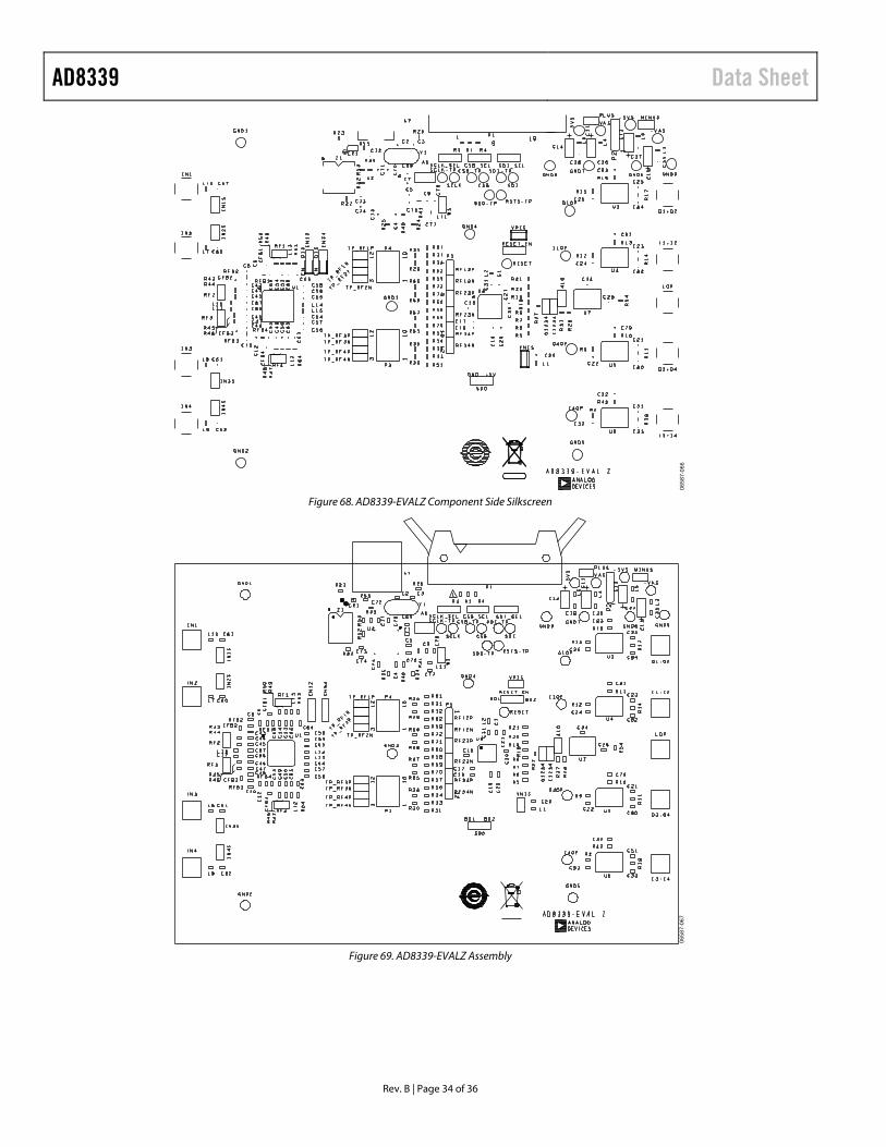
AD8339-EVALZ ARTWORK Figure 66 through Figure 69 show the artwork for the AD8339-EVALZ.
0658
7-06
4
Figure 66. AD8339-EVALZ Component Side Copper
0658
7-06
5
Figure 67. AD8339-EVALZ Wiring Side Copper
AD8339 Data Sheet
Rev. B | Page 34 of 36
0658
7-06
6
Figure 68. AD8339-EVALZ Component Side Silkscreen
0658
7-06
7
Figure 69. AD8339-EVALZ Assembly
Data Sheet AD8339
Rev. B | Page 35 of 36
OUTLINE DIMENSIONS
140
1011
3130
2120
4.254.10 SQ3.95
TOPVIEW
6.00BSC SQ
PIN 1INDICATOR
5.75BSC SQ
12° MAX
0.300.230.18
0.20 REFSEATINGPLANE
1.000.850.80
0.05 MAX0.02 NOM
COPLANARITY0.08
0.80 MAX0.65 TYP
4.50REF
0.500.400.30
0.50BSC
PIN 1INDICATOR
0.60 MAX0.60 MAX
0.25 MIN
EXPOSEDPAD
(BOT TOM VIEW)
COMPLIANT TO JEDEC STANDARDS MO-220-VJJD-2 0721
08-A
FOR PROPER CONNECTION OFTHE EXPOSED PAD, REFER TOTHE PIN CONFIGURATION ANDFUNCTION DESCRIPTIONSSECTION OF THIS DATA SHEET.
Figure 70. 40-Lead Lead Frame Chip Scale Package [LFCSP_VQ]
6 mm × 6 mm Body, Very Thin Quad (CP-40-1)
Dimensions shown in millimeters
ORDERING GUIDE Model1 Temperature Range Package Description Package Option AD8339ACPZ −40°C to +85°C 40-Lead Lead Frame Chip Scale Package [LFCSP_VQ] CP-40-1 AD8339ACPZ-R7 −40°C to +85°C 40-Lead Lead Frame Chip Scale Package [LFCSP_VQ] CP-40-1 AD8339ACPZ-RL −40°C to +85°C 40-Lead Lead Frame Chip Scale Package [LFCSP_VQ] CP-40-1 AD8339-EVALZ Evaluation Board 1 Z = RoHS Compliant Part.

AD8339 Data Sheet
Rev. B | Page 36 of 36
NOTES
©2007–2012 Analog Devices, Inc. All rights reserved. Trademarks and registered trademarks are the property of their respective owners. D06587-0-7/12(B)