dc distribution systems - chalmerswebfiles.portal.chalmers.se/et/lic/nilssondaniellic.pdf · dc...
TRANSCRIPT
THESIS FOR THE DEGREE OF LICENTIATE OF ENGINEERING
DC Distribution Systems
DANIEL NILSSON
Division of Electric Power EngineeringDepartment of Energy and Environment
CHALMERS UNIVERSITY OF TECHNOLOGYGoteborg, Sweden 2005
DC Distribution SystemsDANIEL NILSSON
© DANIEL NILSSON, 2005.
Technical Report at Chalmers University of Technology
Division of Electric Power EngineeringDepartment of Energy and EnvironmentChalmers University of TechnologySE-412 96 GoteborgSwedenTelephone + 46 (0)31-772 1000
Chalmers Bibliotek, ReproserviceGoteborg, Sweden 2005
DC Distribution SystemsDANIEL NILSSONDivision of Electric Power EngineeringDepartment of Energy and EnvironmentChalmers University of Technology
Abstract
In this thesis, the use of direct current for low-voltage distribution systems is investigated.Current trends in the electric power consumption indicate an increasing use of dc in end-userequipment, like computers and other electronic appliances used in households and offices,and in larger equipment used in the industry. With a dc distribution system, power conversionwithin the appliance can be avoided, and losses reduced. The ac/dc conversion is centralized,and by using a fully controllable power-electronic interface, high power quality for both theac and the dc system during steady state and ac grid disturbances can be obtained. Con-nection of back-up energy storage and small-size generation is also easier to realize in a dcsystem.
To facilitate practical application, it is important that the shift from ac to dc distributioncan be done with minimal changes. Results from measurements carried out on commonhousehold appliances reported in this thesis show that most loads are able to operate with dcsupply without any modifications. Furthermore, the measurements are used to derive simple,yet sufficiently accurate, load models. These are used for further analysis of the dc system,both in steady state and during transients, by using the simulation software PSCAD/EMTDC.
To provide a high-quality interface between the ac and dc system, which also allows bi-directional power flow, a Voltage Source Converter (VSC) in series with a Buck converteris proposed, both with controllable output voltages. Three different controllers for the VSCoutput voltage are implemented and tested both in simulations and through experiments ona small laboratory system rated at 3 kVA. The effect of different capacitor sizes, bandwidthsof the controllers and load types is studied. The main conclusion is that the best performanceis shown by the energy-balance dc-link-voltage controller, which only relies on measuringthe dc-link voltage.
In the laboratory setup, the proposed ac/dc interface is used to supply a small dc systemwith four loads, representing a typical office. The system is compared with an identicalsystem supplied with ac, both during steady state and ac grid faults. Measurements showthat the dc system with the proposed interface improves the power quality by balancing thethree ac phase currents and removing low-order harmonics, otherwise present in the currentwhen the loads are supplied with ac. During grid faults, the output dc voltage is maintainedquite constant and the loads are not affected by the disturbance. This test setup provesthat a dc system for low-voltage installations is entirely feasible and can be preferred to aconventional, 50-Hz ac system in applications where many electronic loads are used, highreliability and power quality are desired, and/or low magnetic fields are required.Keywords: direct current (dc), ac/dc interface, Buck converter, current control, distributionsystems, load modeling, power electronics, voltage control, voltage source converter (vsc).
iii

iv

Acknowledgements
This research project has been carried out at the Department of Energy and Environment atChalmers University of Technology. This work has been carried out within Elektra Projectno. 3395 and has been financed by Elforsk, Swedish National Energy Agency and ABBCorporate Research. The financial support is gratefully acknowledged.
I would like to thank my supervisor Dr. Ambra Sannino for all the nice discussions andall the help during this work. Especially the guidance on how to be a perfect conferencedelegate.
I would also like to thank my examiner Prof. Jaap Daalder.The members of the reference group Ingemar Andersson (Goteborg Energi), Anders Las-
son (Volvo), Michael Lindgren (ABB), Johan Swahn (Chalmers) and John Akerlund (UPN)are acknowledged. Thanks for all your comments on the work.
For all the discussions and help I would like to thank Massimo Bongiorno, Stefan Lund-berg, Andreas Petersson and Oskar Wallmark. Robert Karlsson and Magnus Ellsen I wouldlike to thank for the support with the laboratory work. For the nice working environment Iwould like to thank the staff at Elteknik.
I would like to thank my family for their support and love during all these years I havebeen a student at Chalmers.
Finally, I would like to express my deepest gratitude to Lina for her love and understand-ing.
v

vi
Table of Contents
Abstract iii
Acknowledgements v
Table of Contents vii
1 Introduction 11.1 Background and Motivation . . . . . . . . . . . . . . . . . . . . . . . . . 11.2 Aim and Outline of the Thesis . . . . . . . . . . . . . . . . . . . . . . . . 21.3 List of Publications . . . . . . . . . . . . . . . . . . . . . . . . . . . . . . 2
2 DC Distribution Systems 32.1 Historical Background . . . . . . . . . . . . . . . . . . . . . . . . . . . . 32.2 Existing DC Systems . . . . . . . . . . . . . . . . . . . . . . . . . . . . . 4
2.2.1 Telecommunication . . . . . . . . . . . . . . . . . . . . . . . . . . 42.2.2 Vehicles and Ships . . . . . . . . . . . . . . . . . . . . . . . . . . 42.2.3 Traction . . . . . . . . . . . . . . . . . . . . . . . . . . . . . . . . 52.2.4 HVDC . . . . . . . . . . . . . . . . . . . . . . . . . . . . . . . . 5
2.3 Low-Voltage DC Distribution System . . . . . . . . . . . . . . . . . . . . 62.3.1 Reliability . . . . . . . . . . . . . . . . . . . . . . . . . . . . . . . 72.3.2 EMC and Power Quality . . . . . . . . . . . . . . . . . . . . . . . 72.3.3 Loads . . . . . . . . . . . . . . . . . . . . . . . . . . . . . . . . . 82.3.4 Power Generation . . . . . . . . . . . . . . . . . . . . . . . . . . . 82.3.5 Energy Storage . . . . . . . . . . . . . . . . . . . . . . . . . . . . 8
2.4 Low-Voltage DC Distribution System Layout . . . . . . . . . . . . . . . . 82.4.1 Cables . . . . . . . . . . . . . . . . . . . . . . . . . . . . . . . . . 92.4.2 Fuses and Circuit Breakers . . . . . . . . . . . . . . . . . . . . . . 112.4.3 AC/DC Interface . . . . . . . . . . . . . . . . . . . . . . . . . . . 11
2.5 Conclusions . . . . . . . . . . . . . . . . . . . . . . . . . . . . . . . . . . 15
3 Load Modeling 173.1 Introduction . . . . . . . . . . . . . . . . . . . . . . . . . . . . . . . . . . 173.2 Measurement and Analysis . . . . . . . . . . . . . . . . . . . . . . . . . . 173.3 Resistive Loads . . . . . . . . . . . . . . . . . . . . . . . . . . . . . . . . 19
3.3.1 Heaters . . . . . . . . . . . . . . . . . . . . . . . . . . . . . . . . 203.3.2 Lighting . . . . . . . . . . . . . . . . . . . . . . . . . . . . . . . . 21
3.4 Rotating Loads . . . . . . . . . . . . . . . . . . . . . . . . . . . . . . . . 233.5 Electronic Loads . . . . . . . . . . . . . . . . . . . . . . . . . . . . . . . 26
vii
3.5.1 Power Supply . . . . . . . . . . . . . . . . . . . . . . . . . . . . . 273.5.2 Lighting Appliances . . . . . . . . . . . . . . . . . . . . . . . . . 28
3.6 Conclusions . . . . . . . . . . . . . . . . . . . . . . . . . . . . . . . . . . 32
4 Voltage Source Converter and its Control 354.1 Introduction . . . . . . . . . . . . . . . . . . . . . . . . . . . . . . . . . . 354.2 Pulse Width Modulation . . . . . . . . . . . . . . . . . . . . . . . . . . . 364.3 Vector Current Control . . . . . . . . . . . . . . . . . . . . . . . . . . . . 394.4 DC-Link-Voltage Control . . . . . . . . . . . . . . . . . . . . . . . . . . . 44
4.4.1 Energy-Balance DC-Link-Voltage Controller . . . . . . . . . . . . 464.4.2 Load-Current-Feed-Forward DC-Link Voltage Controller . . . . . . 524.4.3 Observer-Load-Current-Feed-Forward DC-Link-Voltage Controller 584.4.4 Transient Performance of DC-Link-Voltage Controllers . . . . . . . 63
4.5 Conclusions . . . . . . . . . . . . . . . . . . . . . . . . . . . . . . . . . . 66
5 Voltage Source Converter with Buck Converter 715.1 Buck Converter . . . . . . . . . . . . . . . . . . . . . . . . . . . . . . . . 715.2 Controller Design . . . . . . . . . . . . . . . . . . . . . . . . . . . . . . . 72
5.2.1 Current Controller . . . . . . . . . . . . . . . . . . . . . . . . . . 725.2.2 Voltage Controller . . . . . . . . . . . . . . . . . . . . . . . . . . 74
5.3 Simulations and Measurements . . . . . . . . . . . . . . . . . . . . . . . . 755.3.1 Load Transients . . . . . . . . . . . . . . . . . . . . . . . . . . . . 765.3.2 Disturbances . . . . . . . . . . . . . . . . . . . . . . . . . . . . . 89
5.4 Conclusions . . . . . . . . . . . . . . . . . . . . . . . . . . . . . . . . . . 89
6 Experimental Setup of a Small DC Network 976.1 Experimental Setup . . . . . . . . . . . . . . . . . . . . . . . . . . . . . . 97
6.1.1 Control System . . . . . . . . . . . . . . . . . . . . . . . . . . . . 976.1.2 VSC . . . . . . . . . . . . . . . . . . . . . . . . . . . . . . . . . . 976.1.3 Buck Converter . . . . . . . . . . . . . . . . . . . . . . . . . . . . 996.1.4 Network Model and Supply . . . . . . . . . . . . . . . . . . . . . 99
6.2 System Start-Up . . . . . . . . . . . . . . . . . . . . . . . . . . . . . . . . 1016.3 Steady-State Operation . . . . . . . . . . . . . . . . . . . . . . . . . . . . 1026.4 Transient Operation . . . . . . . . . . . . . . . . . . . . . . . . . . . . . . 109
6.4.1 Load Changes . . . . . . . . . . . . . . . . . . . . . . . . . . . . . 1096.4.2 Voltage Dips . . . . . . . . . . . . . . . . . . . . . . . . . . . . . 109
6.5 Conclusions . . . . . . . . . . . . . . . . . . . . . . . . . . . . . . . . . . 115
7 Conclusions and Future Work 1177.1 Conclusions . . . . . . . . . . . . . . . . . . . . . . . . . . . . . . . . . . 1177.2 Future Work . . . . . . . . . . . . . . . . . . . . . . . . . . . . . . . . . . 118
References 121
viii
Chapter 1
Introduction
1.1 Background and Motivation
Recent developments and trends in the electric power consumption clearly indicate an in-creasing use of dc in end-user equipment. Computers, TVs, and other electronic-based ap-paratus use low-voltage dc obtained by means of a single-phase rectifier followed by a dcvoltage regulator. In factories, the same input stage is used for process-control equipment,while directly-fed ac machines have been replaced by ac drives that include a two-stageconversion process. Electrical energy production from renewable sources is at dc (as in pho-tovoltaic systems [1] and fuel cells [2]) or requires a similar two-stage conversion as in acdrives, e.g. variable-speed wind turbines and natural-gas microturbines. By using dc fordistribution systems it would thus be possible to skip one stage in the conversion in all thesecases, with consequent savings and higher reliability due to a decreased number of compo-nents. Moreover, energy delivery at dc is characterized by lower losses and voltage drops inlines.
A dc distribution system also allows direct connection of battery blocks for back-upenergy storage. The latter is often needed for avoiding supply interruptions in hospitalsor big office buildings or in industrial complexes with high power quality demands and ispresently implemented with Uninterruptible Power Supply (UPS) systems using two conver-sions (from ac to dc and back). A direct connection to a dc network would thus save twoconversions in this case.
Another advantage of removing the conversion stage in the single pieces of equipmentis that the low-quality EMC problems caused by the conversion equipment, e.g. harmonicpollution, are also removed. One could argue that the problem is only moved somewhereelse, i.e. at the interface between the supplying ac network and the low-voltage dc network,where centralized power conversion is needed. However, as there are only one (or a few)supplying points in such a system, the converter interface can be made more sophisticated inorder to achieve a high power quality. The design and verification of this power-electronicinterface is one of the aims of this thesis. In steady state, it should absorb sinusoidal gridcurrents to have a high power quality. Moreover, it should be able to maintain a stable dcvoltage during load variations on the dc system and disturbances on the ac system. The latteris to prevent that sensitive loads, e.g. computers, trip in case of an ac fault. Finally, in largerdc systems with local power generation, the interface should allow bi-directional power flowto inject the surplus power into the ac system during periods of high generation and lowconsumption in the dc system.
1
Chapter 1. Introduction
Designing a dc distribution system means also dealing with issues, like the choice ofvoltage level, voltage regulation and transformation, system protection and electrical safety,well-established in ac power systems, but little practice exists for dc systems. This in turnrequires analysis tools for dc systems, among others models for steady-state and transientsimulations of different operating conditions. Existing standards for short circuit calcula-tions of dc systems, e.g. IEC 61600 [3] and IEEE Std. 946 [4], describe how to model thecomponents in the system. However, these standards, which are intended for application toauxiliary systems in plants and power stations, which often are dc-based battery systems,give simple models that are not adequate for detailed transient studies. Furthermore, a num-ber of modern loads, which are common in today’s homes and offices, are not covered. Tostudy dc systems, an effort is clearly needed in the field of analysis tools for dc systemanalysis.
1.2 Aim and Outline of the Thesis
The aim of the thesis is to design a high-quality dc distribution system for low-voltage ap-plications. The emphasis is on system modeling and on the design of the power electronicinterface with the ac system. The thesis starts with an overview in Chapter 2 of dc systemsused today and their design .
Many of the existing loads today can be supplied with dc without any modification. Astudy in Chapter 3 presents that common loads can be supplied with dc and for what voltagerange. This is a key issue regarding the selection of a system voltage level. To modelthe steady-state characteristic of the loads and their transient behavior, different tests werecarried out. The study resulted in steady-state and transient models for the loads operatingwith dc voltage.
The design and control of an ac/dc interface is presented in Chapter 4 and 5 togetherwith simulation and measurement results. In this project, an interface consisting of a VoltageSource Converter (VSC) in series with a Buck converter was chosen. Chapter 4 deals withthe three-phase two-level VSC, and Chapter 5 with the VSC in series with a Buck converter.The performance of the interface during different load conditions on the dc side and differentdisturbances on the ac system has been evaluated, together with different control strategies.
The last part of the project was to build a small dc network and supply using an ac/dcinterface. A small system with four loads representing a small office was tested both duringsteady state and during ac faults. The performance of the system was compared with theresult when the loads were supplied directly with ac. The laboratory setup and the measure-ment results are presented in Chapter 6.
1.3 List of Publications
Some of the results of this work have been presented in the following publications:
1. D. Nilsson and A. Sannino, “Efficiency Analysis of Low- and Medium-Voltage dc Systems,”in Proc. IEEE Power Engineering Soc. General Meeting, vol. 2, 2004, pp. 2315-2321.
2. D. Nilsson and A. Sannino, “Load Modelling for Steady-State and Transient Analysis of Low-Voltage dc Systems,” in Conf. Rec. IEEE-IAS Annu. Meeting, vol. 2, 2004, pp. 774-780.
2
Chapter 2
DC Distribution Systems
The first electric power distribution system was built and tested at the end of the 19th century.After that the electrification of the cities began and many distribution systems were builtaround the world. DC systems were dominating in the beginning and it took some yearsbefore ac came strong and replaced the dc systems. The last dc distribution systems inSweden were closed in the 1970’s, but dc systems can still be found in special applications. Inthis chapter a historical background to the “battle of the currents” is given as an introduction.An overview of existing dc systems used in special applications are also presented, with theirpros and cons. Finally, the ideas around a future dc distribution system and how it can bebuilt up are presented.
2.1 Historical Background
In the end of the 19th century, the “battle of the currents” between Thomas Alva Edison andGeorge Westinghouse took place [5]. Edison worked with direct current (dc) systems, andWestinghouse with alternating current (ac) systems. Who won the fight everybody knows,but is ac still the right choice for the 21st century?
When the battle began, cities were illuminated by gas or arc light powered by dc dy-namos. The arc light was produced between two carbon tips and gave a glaring light with anopen flame and noxious fumes, and the tips needed periodically to be renewed. The arc lightwas suitable for streets and in large indoor places like train stations and factories.
Edison saw a possibility to replace the arc lighting with incandescent lamps. The prob-lem of finding a suitable filament was solved when Edison with some ideas from JosephSwan made the carbonized cotton filament burn for more than 13 hours. Edison and histeam developed dc dynamos with constant voltage output, meters, lamp sockets, switchingequipment and fuses. The first incandescent lighting system with a central dc generating sta-tion was demonstrated at Holborn Viaduct in London, England, beginning in January 1882.The more known Pearl Street Station in New York began in September 1882. The successresulted in many installed systems in cities across the continent. Edison’s lighting systemshad some drawbacks. They were operated with low-voltage dc, 100 or 110 V, which resultedin small isolated systems to reduce the losses. A big system would have resulted in a largeamount of copper.
In 1881 the first ac system was demonstrated in London by Lucien Gaulard and JohnGibbs. Westinghouse took the ideas back with him to the U.S., and William Stanley im-
3
Chapter 2. DC Distribution Systems
proved the design. In 1886 the Westinghouse Electric Company had designed equipmentfor an ac lighting system. In 1887 Nikola Tesla filed for seven U.S. patents in the fieldof polyphase ac motors, power transmission, generators, transformers and lighting. West-inghouse purchased these patents, and employed Tesla to develop the ac system. In 1891Westinghouse made history by setting up a 13 mile long transmission line. And many morewould follow [6, 7].
At that time an ac system was a proper choice. The loads were mainly incandescentlamps and machines, and the possibility to transform the voltage from one level to anothermade ac suitable for transmitting electric power over long distances. Also ac machines couldbe made more robust with less maintenance compared with dc machines.
2.2 Existing DC Systems
DC systems can today be found in special applications. It is of interest to investigate where dcsystems can be found and how dc is used before presenting a future dc distribution system.Focus of this part are high power dc systems, and key issues like grid design, operatingvoltage level, voltage control, energy storage, grounding and protection.
2.2.1 Telecommunication
The telecommunication system uses a low-voltage dc power system, and it was developedwhen the centralized battery system was built. The nominal voltage of the system is -48 Vwith the anode connected to ground. The dc system is supplied from the ac mains via voltagecontrolled rectifiers. The system uses transient limiting distribution, i.e. high impedancedistribution, to limit the fault current in case of a short circuit, and to maintain the non-faultedequipment in operation. Battery back-up is installed to supply the system if a disturbanceoccurs on the ac mains. The size of the batteries are 3 to 8 hours of operation [8]. It is alsopossible to have standby generation, e.g. a diesel engine, connected to the system, whichcan be started if the duration of the fault is long. In the beginning the telecommunicationsystem was using copper wire to distribute the phone calls. Today almost all backbonecommunication is going through optical wires. The equipment inside the stations is computerbased and consumes high power. Since the system is using low voltage the currents becomevery high, and studies have therefore been carried out to investigate usage of a higher voltagelevel to reduce the currents [9–11]. A typical telecommunication power system is shown inFig. 2.1.
2.2.2 Vehicles and Ships
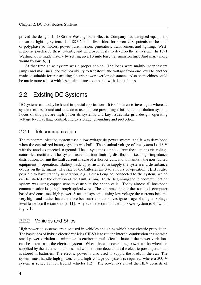
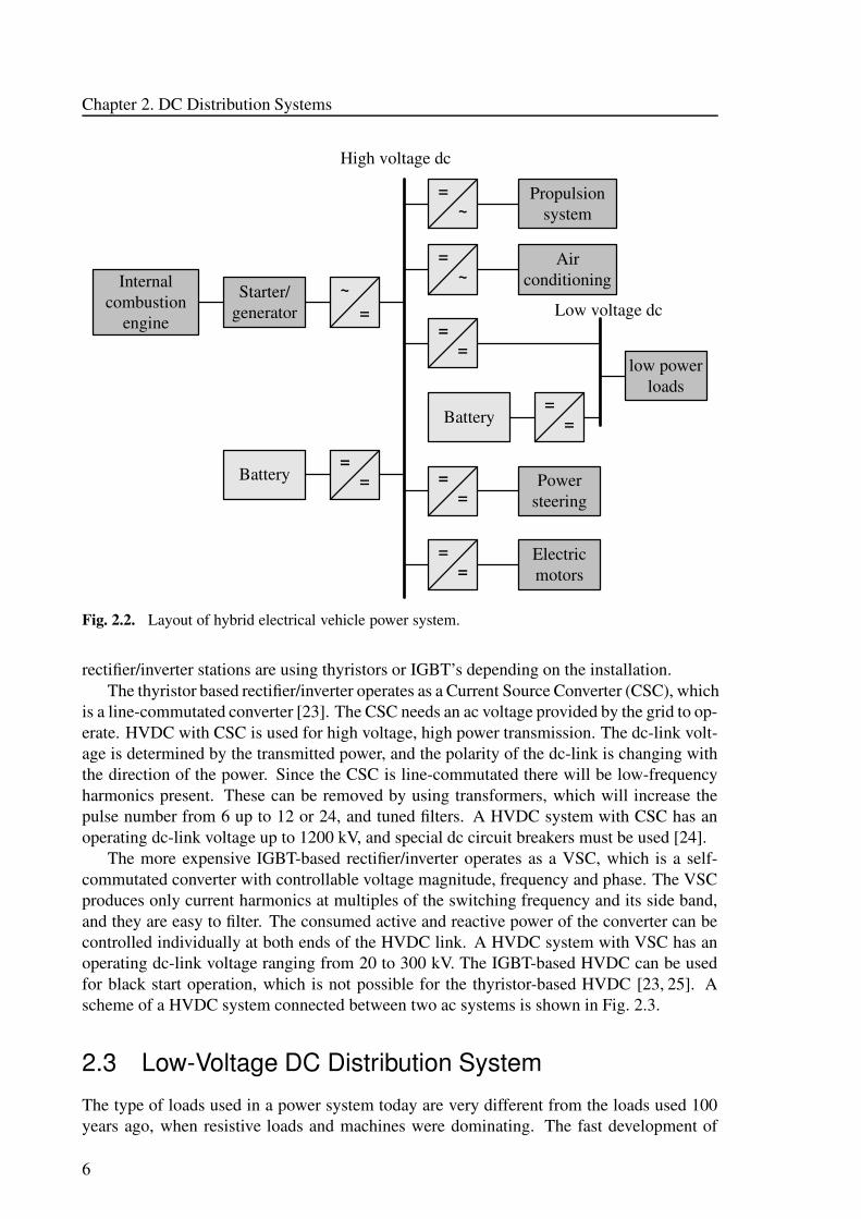
High power dc systems are also used in vehicles and ships which have electric propulsion.The basic idea of hybrid electric vehicles (HEV) is to run the internal combustion engine withsmall power variation to minimize to environmental effects. Instead the power variationscan be taken from the electric system. When the car accelerates, power to the wheels issupplied by the electric machines, and when the car decelerates the electric power generatedis stored in batteries. The electric power is also used to supply the loads in the car. Thesystem must handle high power, and a high voltage dc system is required, where a 300 Vsystem is suited for full hybrid vehicles [12]. The power system of the HEV consists of
4

2.2. Existing DC Systems
Battery
~=
ac loads~=
- 48 Vloads
==Standy
generation
ac mains dc mains - 48 V
other dcloads
24 cells3 or 8 hrs
ac loads
Fig. 2.1. Layout of distribution system for telecommunication.
starter/generator (engine), electric machine with associated converter, energy storage (batteryor supercaps) with associated chargers, converters to adjust high voltage to required loadvoltage, see Fig. 2.2 [13–15].
Ships can also use an electric propulsion system [16]. The electric power is generatedby diesel engines, and used for supplying electric loads and the electric machines used forpropulsion. The electric system uses both ac or dc depending on the application [17]. Navalships and submarines use also other types of power sources like stirling machines or nuclearpower, which can be used underwater. Eliminating the mechanical link between the powerplant and the propulsor will enable reduction of noise and vibrations, which is important tominimize the risk of detection [18–20].
2.2.3 Traction
DC has been used for a long time in traction systems, and the reason is because dc machinesare very easy to speed control by simply changing the series resistance. The traction powersystem is supplied from the ac systems via six, 12 or 24-pulse rectifiers depending on theconfiguration [21]. A higher number will reduce the current ripple. Standard voltages are600 or 750 V for urban metros and 1.5 up to 3 kV for regional systems [22]. The power issupplied to the train through a conductor rail laid on insulators on one side of the runningrail, or through an overhead catenary. The return path is usually the grounded tracks. Thedc power systems is protected by circuit breakers controlled by relays which will trip thebreakers in case of overcurrent, ground fault and short circuits. Today ac machines are moreused than dc machines due to less maintenance, and this requires inverters which are veryconvenient to supply with dc. AC is more economical to use for high-speed trains, whichconsume high power.
2.2.4 HVDC
High Voltage DC (HVDC) is a technique to transmit electric power using dc voltage insteadof ac voltage. HVDC makes it possible to transmit power over a long distance or usingunderground cable. The absence of reactive power decreases the losses. Another advan-tage with HVDC is that two ac systems with different frequency can be connected. The
5
Chapter 2. DC Distribution Systems
Propulsionsystem~
=
Powersteering
==
High voltage dc
low powerloads
Battery
Battery
==
==
Low voltage dc
Internalcombustion
engine
Starter/generator
==
~=
==
Electricmotors
Airconditioning~
=
Fig. 2.2. Layout of hybrid electrical vehicle power system.
rectifier/inverter stations are using thyristors or IGBT’s depending on the installation.The thyristor based rectifier/inverter operates as a Current Source Converter (CSC), which
is a line-commutated converter [23]. The CSC needs an ac voltage provided by the grid to op-erate. HVDC with CSC is used for high voltage, high power transmission. The dc-link volt-age is determined by the transmitted power, and the polarity of the dc-link is changing withthe direction of the power. Since the CSC is line-commutated there will be low-frequencyharmonics present. These can be removed by using transformers, which will increase thepulse number from 6 up to 12 or 24, and tuned filters. A HVDC system with CSC has anoperating dc-link voltage up to 1200 kV, and special dc circuit breakers must be used [24].
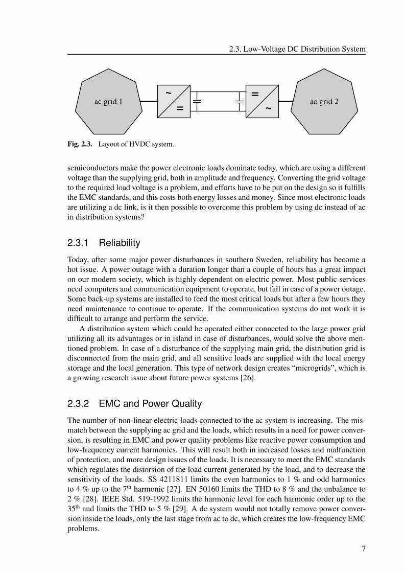
The more expensive IGBT-based rectifier/inverter operates as a VSC, which is a self-commutated converter with controllable voltage magnitude, frequency and phase. The VSCproduces only current harmonics at multiples of the switching frequency and its side band,and they are easy to filter. The consumed active and reactive power of the converter can becontrolled individually at both ends of the HVDC link. A HVDC system with VSC has anoperating dc-link voltage ranging from 20 to 300 kV. The IGBT-based HVDC can be usedfor black start operation, which is not possible for the thyristor-based HVDC [23, 25]. Ascheme of a HVDC system connected between two ac systems is shown in Fig. 2.3.
2.3 Low-Voltage DC Distribution System
The type of loads used in a power system today are very different from the loads used 100years ago, when resistive loads and machines were dominating. The fast development of
6
2.3. Low-Voltage DC Distribution System
~= ~
=ac grid 1 ac grid 2
Fig. 2.3. Layout of HVDC system.
semiconductors make the power electronic loads dominate today, which are using a differentvoltage than the supplying grid, both in amplitude and frequency. Converting the grid voltageto the required load voltage is a problem, and efforts have to be put on the design so it fulfillsthe EMC standards, and this costs both energy losses and money. Since most electronic loadsare utilizing a dc link, is it then possible to overcome this problem by using dc instead of acin distribution systems?
2.3.1 Reliability
Today, after some major power disturbances in southern Sweden, reliability has become ahot issue. A power outage with a duration longer than a couple of hours has a great impacton our modern society, which is highly dependent on electric power. Most public servicesneed computers and communication equipment to operate, but fail in case of a power outage.Some back-up systems are installed to feed the most critical loads but after a few hours theyneed maintenance to continue to operate. If the communication systems do not work it isdifficult to arrange and perform the service.
A distribution system which could be operated either connected to the large power gridutilizing all its advantages or in island in case of disturbances, would solve the above men-tioned problem. In case of a disturbance of the supplying main grid, the distribution grid isdisconnected from the main grid, and all sensitive loads are supplied with the local energystorage and the local generation. This type of network design creates “microgrids”, which isa growing research issue about future power systems [26].
2.3.2 EMC and Power Quality
The number of non-linear electric loads connected to the ac system is increasing. The mis-match between the supplying ac grid and the loads, which results in a need for power conver-sion, is resulting in EMC and power quality problems like reactive power consumption andlow-frequency current harmonics. This will result both in increased losses and malfunctionof protection, and more design issues of the loads. It is necessary to meet the EMC standardswhich regulates the distorsion of the load current generated by the load, and to decrease thesensitivity of the loads. SS 4211811 limits the even harmonics to 1 % and odd harmonicsto 4 % up to the 7th harmonic [27]. EN 50160 limits the THD to 8 % and the unbalance to2 % [28]. IEEE Std. 519-1992 limits the harmonic level for each harmonic order up to the35th and limits the THD to 5 % [29]. A dc system would not totally remove power conver-sion inside the loads, only the last stage from ac to dc, which creates the low-frequency EMCproblems.
7
Chapter 2. DC Distribution Systems
2.3.3 Loads
The electrical appliances today are designed to operate with ac, but many of them can runon dc without modification. All resistive loads like heaters, incandescent lamps, stoves, op-erate with both ac and dc, and the output power is equal if the RMS values are the same.All electronic loads like computers, fluorescent lamps with electronic ballast, flat screen TV,battery charger, which all internally use dc, have a bridge rectifier to convert ac to dc. Thisrectification will introduce current harmonics, which have a negative effect on the powersystem: neutral conductors become overloaded and protections malfunction. All these elec-tronic loads can directly be supplied with dc. Rotating loads driven by a universal machine,or frequency controlled machines can also be supplied with dc. Problems arise with loadsusing a fix speed ac machine which utilizes a virtual phase created by a reactive componentto get a rotating magnetic field. Loads with inductive parts cannot be supplied with dc, sincedc creates a constant increasing current through it. Also loads with mechanical breakersdesigned for ac voltage cannot be supplied with dc. The breaker will be destroyed whenbreaking dc, due to no natural current zero. Loads supplied with dc are further treated inChapter 3.
2.3.4 Power Generation
The number of alternative generation sources connected to the distribution system increases[30]. Some of them, like photovoltaic and fuel cells, produce dc, and they can easily beconnected to a dc distribution system directly, or through a dc/dc-converter. Microturbines,generating high-frequency ac, which is very suitable to convert to dc due to the high fre-quency, is also easy to connect to a dc system. Connecting the generation to an ac systemusing converters generating a synchronized sinusoidal ac current is more complicated, re-garding both design and control.
The electric power output of a wind turbine can be kept at a maximum if the speedof the turbine is allowed to vary. If the shaft is directly connected to the generator thefrequency will vary with the wind speed, and this is not possible if the electric output hasto be synchronized to the grid. To overcome this problem an ac/dc/ac-converter can be usedwhich is an expensive solution. A cheaper and simpler solution is to connect an ac/dc-converter to a dc grid. Other types of generators operating with varying speed are hydro andtidal generators.
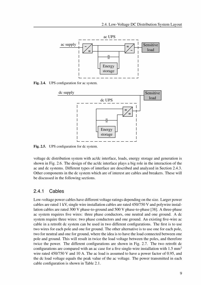
2.3.5 Energy Storage
UPS are used to supply sensitive loads in an ac systems. The UPS configuration for anac system, shown in Fig. 2.4, consists of an ac/dc-converter, energy storage and a dc/ac-converter. Supplying sensitive loads with dc requires only a simple dc/dc-converter insteadof two ac/dc-converters, which is shown in Fig. 2.5. Both components and losses can bereduced.
2.4 Low-Voltage DC Distribution System Layout
The idea of using low-voltage dc distribution systems has been analyzed in pre studies of dcsystems [31–37]. Also some test facilities are planned to evaluate such a system. A low-
8
2.4. Low-Voltage DC Distribution System Layout
~=~
=
Energystorage
ac UPS
Sensitiveload
ac supply
Fig. 2.4. UPS configuration for ac system.
=
Energystorage
dc UPS
=
Sensitiveload
dc supply
Fig. 2.5. UPS configuration for dc system.
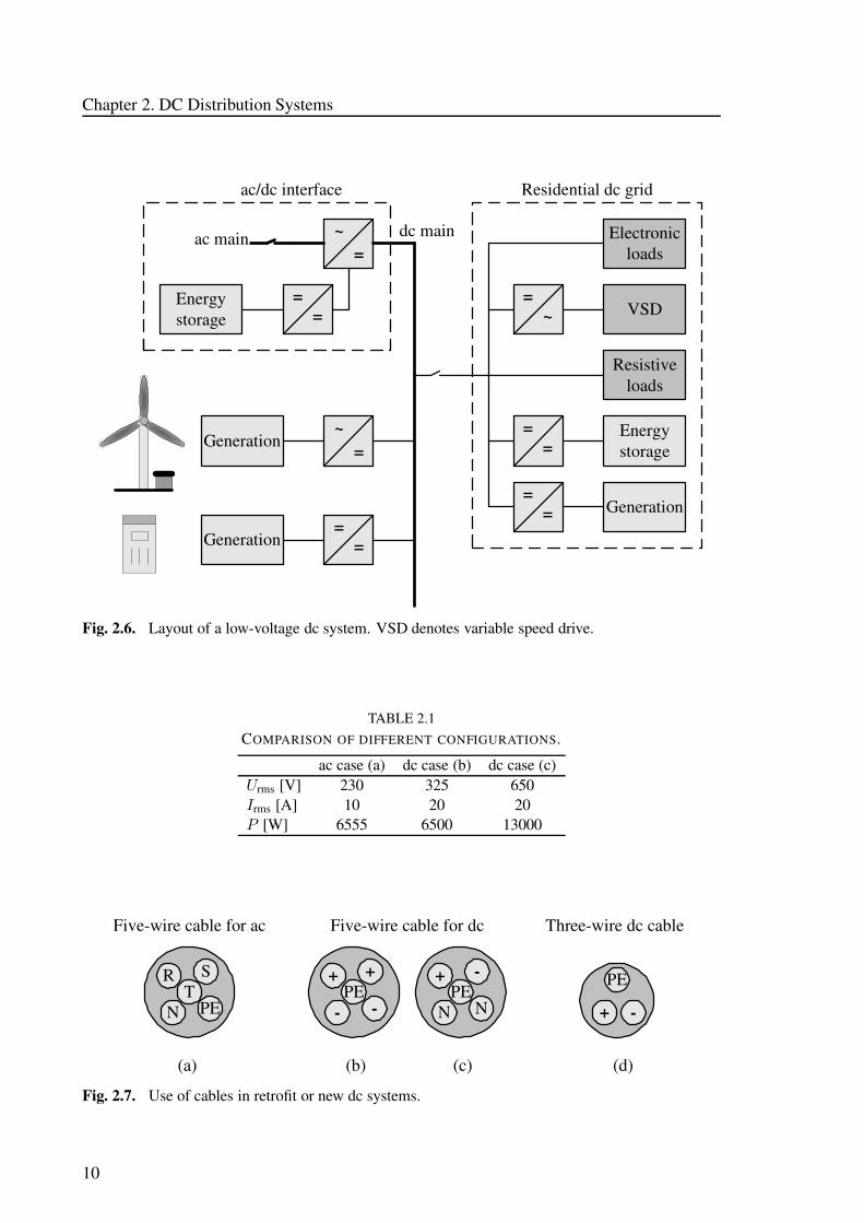
voltage dc distribution system with ac/dc interface, loads, energy storage and generation isshown in Fig. 2.6. The design of the ac/dc interface plays a big role in the interaction of theac and dc systems. Different types of interface are described and analyzed in Section 2.4.3.Other components in the dc system which are of interest are cables and breakers. These willbe discussed in the following sections.
2.4.1 Cables
Low-voltage power cables have different voltage ratings depending on the size. Larger powercables are rated 1 kV, single wire installation cables are rated 450/750 V and polywire instal-lation cables are rated 300 V phase-to-ground and 500 V phase-to-phase [38]. A three-phaseac system requires five wires: three phase conductors, one neutral and one ground. A dcsystem require three wires: two phase conductors and one ground. An existing five-wire accable in a retrofit dc system can be used in two different configurations. The first is to usetwo wires for each pole and one for ground. The other alternative is to use one for each pole,two for neutral and one for ground, where the idea is to have the load connected between onepole and ground. This will result in twice the load voltage between the poles, and thereforetwice the power. The different configurations are shown in Fig. 2.7. The two retrofit dcconfigurations are compared with an ac case for a five single-wire installation with 1.5 mm2
wire rated 450/750 V and 10 A. The ac load is assumed to have a power factor of 0.95, andthe dc load voltage equals the peak value of the ac voltage. The power transmitted in eachcable configuration is shown in Table 2.1.
9
Chapter 2. DC Distribution Systems
Energystorage
Electronicloads
Residential dc grid
~=
VSD~=
Resistiveloads
==
Generation=
=
Energystorage
==
Generation
Generation=
=
ac/dc interface
ac main dc main
~=
Fig. 2.6. Layout of a low-voltage dc system. VSD denotes variable speed drive.
TABLE 2.1COMPARISON OF DIFFERENT CONFIGURATIONS.
ac case (a) dc case (b) dc case (c)Urms [V] 230 325 650Irms [A] 10 20 20P [W] 6555 6500 13000
Five-wire cable for ac Five-wire cable for dc Three-wire dc cable
PEN
R ST
--
+ +PE
PE
+ -NN
+ -PE
(a) (b) (c) (d)
Fig. 2.7. Use of cables in retrofit or new dc systems.
10
2.4. Low-Voltage DC Distribution System Layout
2.4.2 Fuses and Circuit Breakers
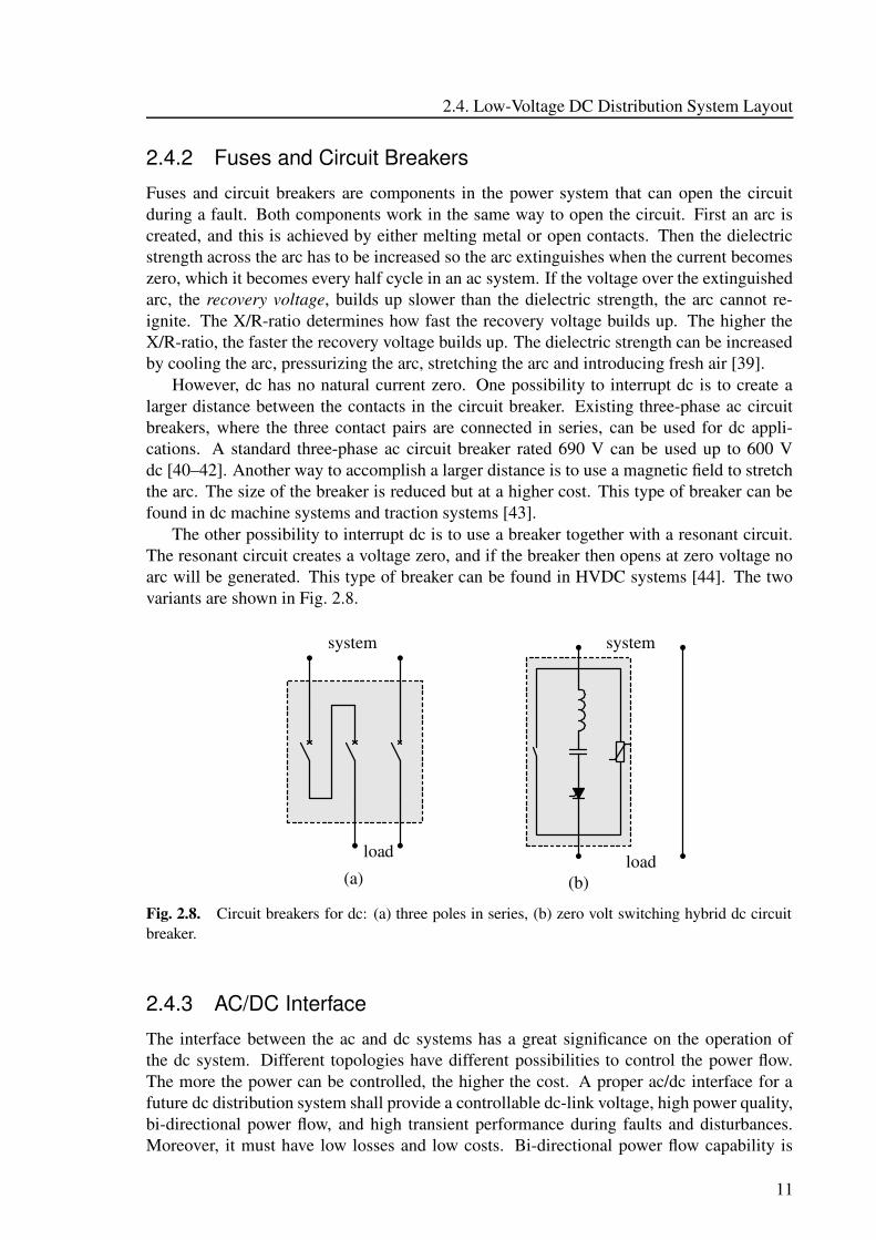
Fuses and circuit breakers are components in the power system that can open the circuitduring a fault. Both components work in the same way to open the circuit. First an arc iscreated, and this is achieved by either melting metal or open contacts. Then the dielectricstrength across the arc has to be increased so the arc extinguishes when the current becomeszero, which it becomes every half cycle in an ac system. If the voltage over the extinguishedarc, the recovery voltage, builds up slower than the dielectric strength, the arc cannot re-ignite. The X/R-ratio determines how fast the recovery voltage builds up. The higher theX/R-ratio, the faster the recovery voltage builds up. The dielectric strength can be increasedby cooling the arc, pressurizing the arc, stretching the arc and introducing fresh air [39].
However, dc has no natural current zero. One possibility to interrupt dc is to create alarger distance between the contacts in the circuit breaker. Existing three-phase ac circuitbreakers, where the three contact pairs are connected in series, can be used for dc appli-cations. A standard three-phase ac circuit breaker rated 690 V can be used up to 600 Vdc [40–42]. Another way to accomplish a larger distance is to use a magnetic field to stretchthe arc. The size of the breaker is reduced but at a higher cost. This type of breaker can befound in dc machine systems and traction systems [43].
The other possibility to interrupt dc is to use a breaker together with a resonant circuit.The resonant circuit creates a voltage zero, and if the breaker then opens at zero voltage noarc will be generated. This type of breaker can be found in HVDC systems [44]. The twovariants are shown in Fig. 2.8.
(a) (b)
system system
load load
Fig. 2.8. Circuit breakers for dc: (a) three poles in series, (b) zero volt switching hybrid dc circuitbreaker.
2.4.3 AC/DC Interface
The interface between the ac and dc systems has a great significance on the operation ofthe dc system. Different topologies have different possibilities to control the power flow.The more the power can be controlled, the higher the cost. A proper ac/dc interface for afuture dc distribution system shall provide a controllable dc-link voltage, high power quality,bi-directional power flow, and high transient performance during faults and disturbances.Moreover, it must have low losses and low costs. Bi-directional power flow capability is
11
Chapter 2. DC Distribution Systems
necessary if it shall be possible to transfer power from the dc system to the ac system duringlow-load, high-generation condition in the dc system. Galvanic isolation prevents having apath between the ac and dc systems in case of a fault. Five different topologies of ac/dcinterfaces from no control to full control are presented in this section.
Diode rectifier
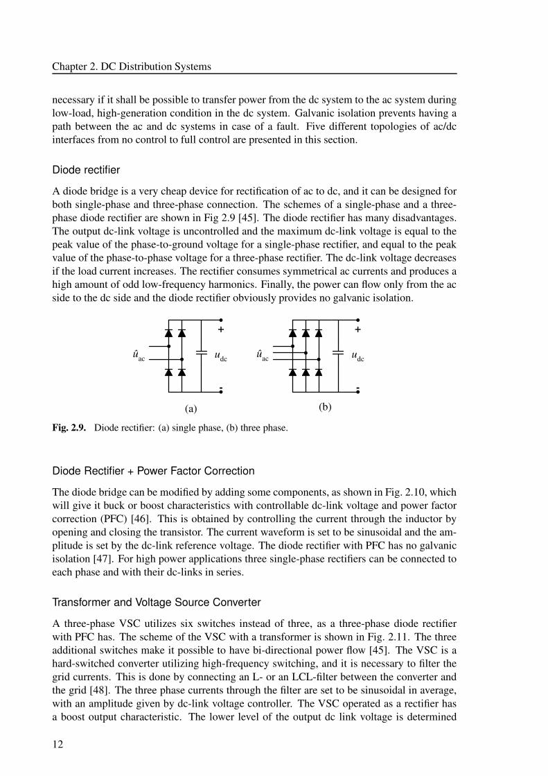
A diode bridge is a very cheap device for rectification of ac to dc, and it can be designed forboth single-phase and three-phase connection. The schemes of a single-phase and a three-phase diode rectifier are shown in Fig 2.9 [45]. The diode rectifier has many disadvantages.The output dc-link voltage is uncontrolled and the maximum dc-link voltage is equal to thepeak value of the phase-to-ground voltage for a single-phase rectifier, and equal to the peakvalue of the phase-to-phase voltage for a three-phase rectifier. The dc-link voltage decreasesif the load current increases. The rectifier consumes symmetrical ac currents and produces ahigh amount of odd low-frequency harmonics. Finally, the power can flow only from the acside to the dc side and the diode rectifier obviously provides no galvanic isolation.
ûac udc
+
-
ûac udc
+
-
(a) (b)
Fig. 2.9. Diode rectifier: (a) single phase, (b) three phase.
Diode Rectifier + Power Factor Correction
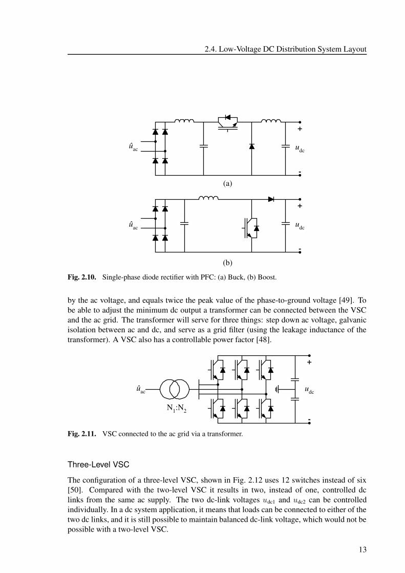
The diode bridge can be modified by adding some components, as shown in Fig. 2.10, whichwill give it buck or boost characteristics with controllable dc-link voltage and power factorcorrection (PFC) [46]. This is obtained by controlling the current through the inductor byopening and closing the transistor. The current waveform is set to be sinusoidal and the am-plitude is set by the dc-link reference voltage. The diode rectifier with PFC has no galvanicisolation [47]. For high power applications three single-phase rectifiers can be connected toeach phase and with their dc-links in series.
Transformer and Voltage Source Converter
A three-phase VSC utilizes six switches instead of three, as a three-phase diode rectifierwith PFC has. The scheme of the VSC with a transformer is shown in Fig. 2.11. The threeadditional switches make it possible to have bi-directional power flow [45]. The VSC is ahard-switched converter utilizing high-frequency switching, and it is necessary to filter thegrid currents. This is done by connecting an L- or an LCL-filter between the converter andthe grid [48]. The three phase currents through the filter are set to be sinusoidal in average,with an amplitude given by dc-link voltage controller. The VSC operated as a rectifier hasa boost output characteristic. The lower level of the output dc link voltage is determined
12
2.4. Low-Voltage DC Distribution System Layout
ûac udc
+
-
ûac udc
+
-(a)
(b)
Fig. 2.10. Single-phase diode rectifier with PFC: (a) Buck, (b) Boost.
by the ac voltage, and equals twice the peak value of the phase-to-ground voltage [49]. Tobe able to adjust the minimum dc output a transformer can be connected between the VSCand the ac grid. The transformer will serve for three things: step down ac voltage, galvanicisolation between ac and dc, and serve as a grid filter (using the leakage inductance of thetransformer). A VSC also has a controllable power factor [48].
N1:N2
udcûac
+
-
Fig. 2.11. VSC connected to the ac grid via a transformer.
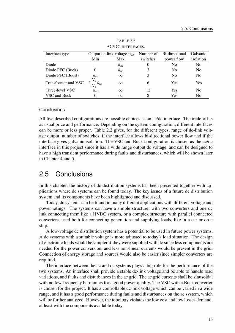
Three-Level VSC
The configuration of a three-level VSC, shown in Fig. 2.12 uses 12 switches instead of six[50]. Compared with the two-level VSC it results in two, instead of one, controlled dclinks from the same ac supply. The two dc-link voltages udc1 and udc2 can be controlledindividually. In a dc system application, it means that loads can be connected to either of thetwo dc links, and it is still possible to maintain balanced dc-link voltage, which would not bepossible with a two-level VSC.
13
Chapter 2. DC Distribution Systems
ûac
udc1
+
-
udc2
+
-
Fig. 2.12. Three-level VSC.
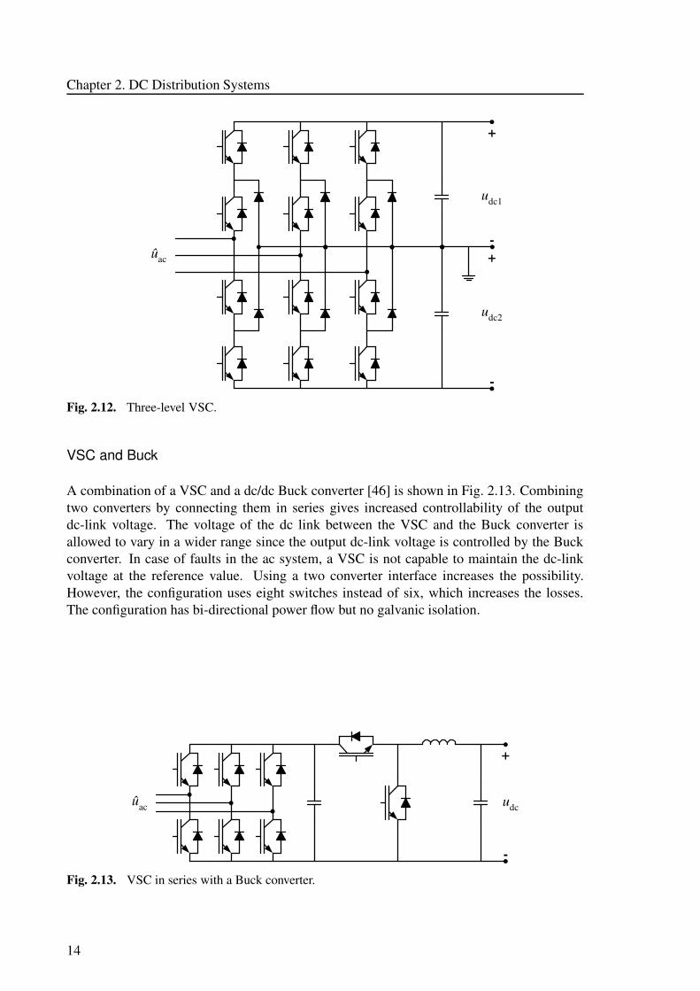
VSC and Buck
A combination of a VSC and a dc/dc Buck converter [46] is shown in Fig. 2.13. Combiningtwo converters by connecting them in series gives increased controllability of the outputdc-link voltage. The voltage of the dc link between the VSC and the Buck converter isallowed to vary in a wider range since the output dc-link voltage is controlled by the Buckconverter. In case of faults in the ac system, a VSC is not capable to maintain the dc-linkvoltage at the reference value. Using a two converter interface increases the possibility.However, the configuration uses eight switches instead of six, which increases the losses.The configuration has bi-directional power flow but no galvanic isolation.
ûac udc
+
-
Fig. 2.13. VSC in series with a Buck converter.
14
2.5. Conclusions
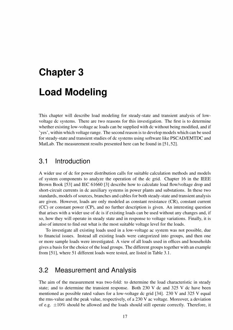
TABLE 2.2AC/DC INTERFACES.
Interface type Output dc-link voltage udc Number of Bi-directional GalvanicMin Max switches power flow isolation
Diode - uac 0 No NoDiode PFC (Buck) 0 uac 3 No NoDiode PFC (Boost) uac ∞ 3 No No
Transformer and VSC 2N2
N1
uac ∞ 6 Yes Yes
Three-level VSC uac ∞ 12 Yes NoVSC and Buck 0 ∞ 8 Yes No
Conclusions
All five described configurations are possible choices as an ac/dc interface. The trade-off isas usual price and performance. Depending on the system configuration, different interfacescan be more or less proper. Table 2.2 gives, for the different types, range of dc-link volt-age output, number of switches, if the interface allows bi-directional power flow and if theinterface gives galvanic isolation. The VSC and Buck configuration is chosen as the ac/dcinterface in this project since it has a wide range output dc voltage, and can be designed tohave a high transient performance during faults and disturbances, which will be shown laterin Chapter 4 and 5.
2.5 Conclusions
In this chapter, the history of dc distribution systems has been presented together with ap-plications where dc systems can be found today. The key issues of a future dc distributionsystem and its components have been highlighted and discussed.
Today, dc systems can be found in many different applications with different voltage andpower ratings. The systems can have a simple structure, with two converters and one dclink connecting them like a HVDC system, or a complex structure with parallel connectedconverters, used both for connecting generation and supplying loads, like in a car or on aship.
A low-voltage dc distribution system has a potential to be used in future power systems.A dc systems with a suitable voltage is more adjusted to today’s load situation. The designof electronic loads would be simpler if they were supplied with dc since less components areneeded for the power conversion, and less non-linear currents would be present in the grid.Connection of energy storage and sources would also be easier since simpler converters arerequired.
The interface between the ac and dc systems plays a big role for the performance of thetwo systems. An interface shall provide a stable dc-link voltage and be able to handle loadvariations, and faults and disturbances in the ac grid. The ac grid currents shall be sinusoidalwith no low-frequency harmonics for a good power quality. The VSC with a Buck converteris chosen for the project. It has a controllable dc-link voltage which can be varied in a widerange, and it has a good performance during faults and disturbances on the ac system, whichwill be further analyzed. However, the topology violates the low cost and low losses demand,at least with the components available today.
15

Chapter 3
Load Modeling
This chapter will describe load modeling for steady-state and transient analysis of low-voltage dc systems. There are two reasons for this investigation. The first is to determinewhether existing low-voltage ac loads can be supplied with dc without being modified, and if’yes’, within which voltage range. The second reason is to develop models which can be usedfor steady-state and transient studies of dc systems using software like PSCAD/EMTDC andMatLab. The measurement results presented here can be found in [51, 52].
3.1 Introduction
A wider use of dc for power distribution calls for suitable calculation methods and modelsof system components to analyze the operation of the dc grid. Chapter 16 in the IEEEBrown Book [53] and IEC 61660 [3] describe how to calculate load flow/voltage drop andshort-circuit currents in dc auxiliary systems in power plants and substations. In these twostandards, models of sources, branches and cables for both steady-state and transient analysisare given. However, loads are only modeled as constant resistance (CR), constant current(CC) or constant power (CP), and no further description is given. An interesting questionthat arises with a wider use of dc is if existing loads can be used without any changes and, ifso, how they will operate in steady state and in response to voltage variations. Finally, it isalso of interest to find out what is the most suitable voltage level for the loads.
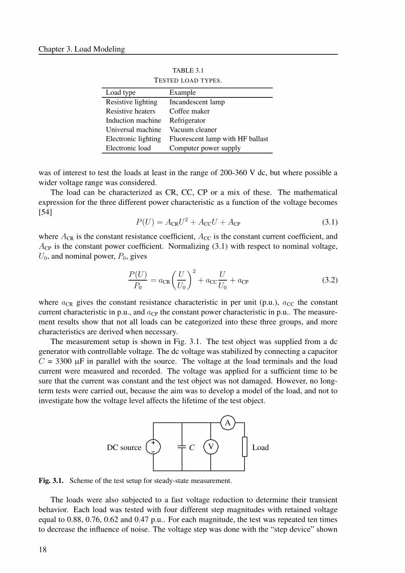
To investigate all existing loads used in a low-voltage ac system was not possible, dueto financial issues. Instead all existing loads were categorized into groups, and then oneor more sample loads were investigated. A view of all loads used in offices and householdsgives a basis for the choice of the load groups. The different groups together with an examplefrom [51], where 51 different loads were tested, are listed in Table 3.1.
3.2 Measurement and Analysis
The aim of the measurement was two-fold: to determine the load characteristic in steadystate; and to determine the transient response. Both 230 V dc and 325 V dc have beenmentioned as possible rated values for a low-voltage dc grid [34]. 230 V and 325 V equalthe rms-value and the peak value, respectively, of a 230 V ac voltage. Moreover, a deviationof e.g. ±10% should be allowed and the loads should still operate correctly. Therefore, it
17
Chapter 3. Load Modeling
TABLE 3.1TESTED LOAD TYPES.
Load type ExampleResistive lighting Incandescent lampResistive heaters Coffee makerInduction machine RefrigeratorUniversal machine Vacuum cleanerElectronic lighting Fluorescent lamp with HF ballastElectronic load Computer power supply
was of interest to test the loads at least in the range of 200-360 V dc, but where possible awider voltage range was considered.
The load can be characterized as CR, CC, CP or a mix of these. The mathematicalexpression for the three different power characteristic as a function of the voltage becomes[54]
P (U) = ACRU2 + ACCU + ACP (3.1)
where ACR is the constant resistance coefficient, ACC is the constant current coefficient, andACP is the constant power coefficient. Normalizing (3.1) with respect to nominal voltage,U0, and nominal power, P0, gives
P (U)
P0
= aCR
(
U
U0
)2
+ aCCU
U0
+ aCP (3.2)
where aCR gives the constant resistance characteristic in per unit (p.u.), aCC the constantcurrent characteristic in p.u., and aCP the constant power characteristic in p.u.. The measure-ment results show that not all loads can be categorized into these three groups, and morecharacteristics are derived when necessary.
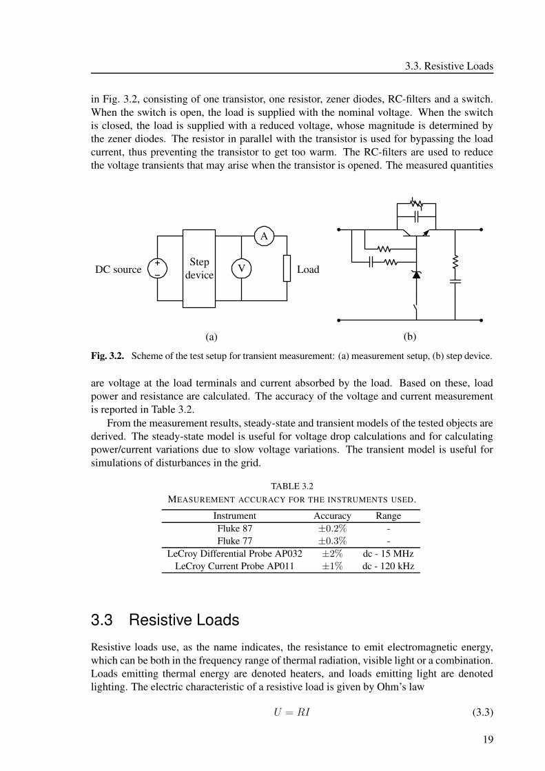
The measurement setup is shown in Fig. 3.1. The test object was supplied from a dcgenerator with controllable voltage. The dc voltage was stabilized by connecting a capacitorC = 3300 µF in parallel with the source. The voltage at the load terminals and the loadcurrent were measured and recorded. The voltage was applied for a sufficient time to besure that the current was constant and the test object was not damaged. However, no long-term tests were carried out, because the aim was to develop a model of the load, and not toinvestigate how the voltage level affects the lifetime of the test object.
A
V LoadCDC source
Fig. 3.1. Scheme of the test setup for steady-state measurement.
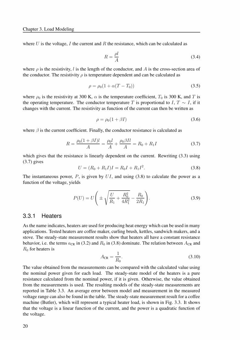
The loads were also subjected to a fast voltage reduction to determine their transientbehavior. Each load was tested with four different step magnitudes with retained voltageequal to 0.88, 0.76, 0.62 and 0.47 p.u.. For each magnitude, the test was repeated ten timesto decrease the influence of noise. The voltage step was done with the “step device” shown
18
3.3. Resistive Loads
in Fig. 3.2, consisting of one transistor, one resistor, zener diodes, RC-filters and a switch.When the switch is open, the load is supplied with the nominal voltage. When the switchis closed, the load is supplied with a reduced voltage, whose magnitude is determined bythe zener diodes. The resistor in parallel with the transistor is used for bypassing the loadcurrent, thus preventing the transistor to get too warm. The RC-filters are used to reducethe voltage transients that may arise when the transistor is opened. The measured quantities
A
V LoadDC sourceStep
device
(a) (b)
Fig. 3.2. Scheme of the test setup for transient measurement: (a) measurement setup, (b) step device.
are voltage at the load terminals and current absorbed by the load. Based on these, loadpower and resistance are calculated. The accuracy of the voltage and current measurementis reported in Table 3.2.
From the measurement results, steady-state and transient models of the tested objects arederived. The steady-state model is useful for voltage drop calculations and for calculatingpower/current variations due to slow voltage variations. The transient model is useful forsimulations of disturbances in the grid.
TABLE 3.2MEASUREMENT ACCURACY FOR THE INSTRUMENTS USED.
Instrument Accuracy RangeFluke 87 ±0.2% -Fluke 77 ±0.3% -
LeCroy Differential Probe AP032 ±2% dc - 15 MHzLeCroy Current Probe AP011 ±1% dc - 120 kHz
3.3 Resistive Loads
Resistive loads use, as the name indicates, the resistance to emit electromagnetic energy,which can be both in the frequency range of thermal radiation, visible light or a combination.Loads emitting thermal energy are denoted heaters, and loads emitting light are denotedlighting. The electric characteristic of a resistive load is given by Ohm’s law
U = RI (3.3)
19
Chapter 3. Load Modeling
where U is the voltage, I the current and R the resistance, which can be calculated as
R =ρl
A(3.4)
where ρ is the resistivity, l is the length of the conductor, and A is the cross-section area ofthe conductor. The resistivity ρ is temperature dependent and can be calculated as
ρ = ρ0(1 + α(T − T0)) (3.5)
where ρ0 is the resistivity at 300 K, α is the temperature coefficient, T0 is 300 K, and T isthe operating temperature. The conductor temperature T is proportional to I , T ∼ I , if itchanges with the current. The resistivity as function of the current can then be written as
ρ = ρ0(1 + βI) (3.6)
where β is the current coefficient. Finally, the conductor resistance is calculated as
R =ρ0(1 + βI)l
A=
ρ0l
A+
ρ0βIl
A= R0 + R1I (3.7)
which gives that the resistance is linearly dependent on the current. Rewriting (3.3) using(3.7) gives
U = (R0 + R1I)I = R0I + R1I2. (3.8)
The instantaneous power, P , is given by UI , and using (3.8) to calculate the power as afunction of the voltage, yields
P (U) = U
(
±
√
U
R1
+R2
0
4R21
−R0
2R1
)
. (3.9)
3.3.1 Heaters
As the name indicates, heaters are used for producing heat energy which can be used in manyapplications. Tested heaters are coffee maker, curling brush, kettles, sandwich makers, and astove. The steady-state measurement results show that heaters all have a constant resistancebehavior, i.e. the terms aCR in (3.2) and R0 in (3.8) dominate. The relation between ACR andR0 for heaters is
ACR =1
R0
. (3.10)
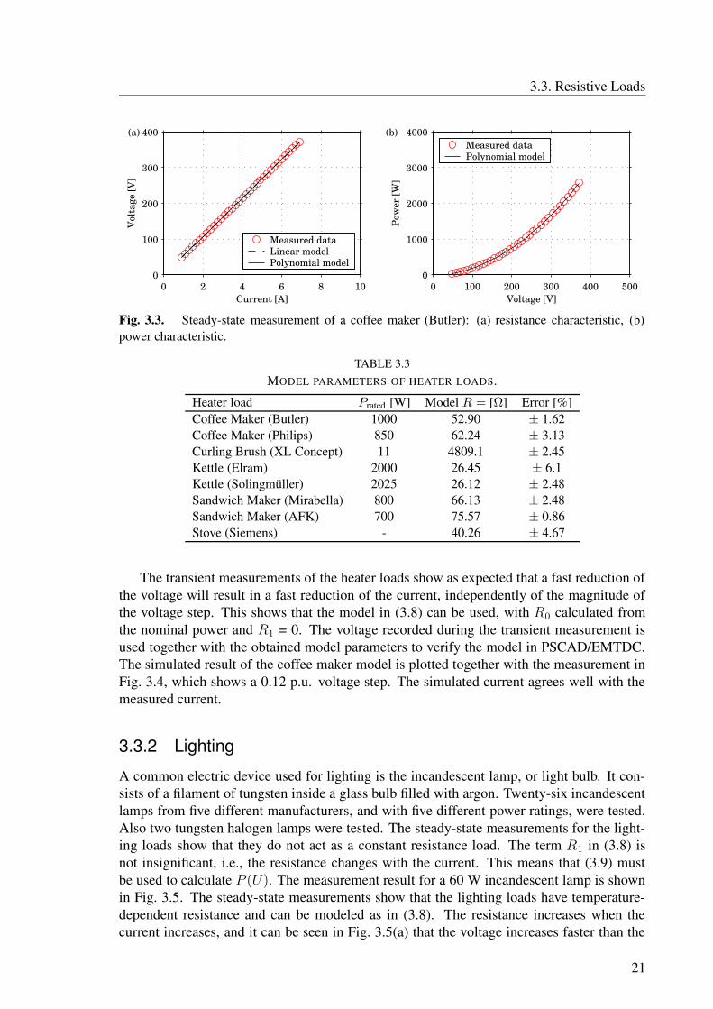
The value obtained from the measurements can be compared with the calculated value usingthe nominal power given for each load. The steady-state model of the heaters is a pureresistance calculated from the nominal power, if it is given. Otherwise, the value obtainedfrom the measurements is used. The resulting models of the steady-state measurements arereported in Table 3.3. An average error between model and measurement in the measuredvoltage range can also be found in the table. The steady-state measurement result for a coffeemachine (Butler), which will represent a typical heater load, is shown in Fig. 3.3. It showsthat the voltage is a linear function of the current, and the power is a quadratic function ofthe voltage.
20
3.3. Resistive Loads
0 2 4 6 8 100
100
200
300
400
Current [A]
Vol
tage
[V]
(a)
Measured dataLinear modelPolynomial model
0 100 200 300 400 5000
1000
2000
3000
4000
Voltage [V]
Pow
er [W
]
(b)Measured dataPolynomial model
Fig. 3.3. Steady-state measurement of a coffee maker (Butler): (a) resistance characteristic, (b)power characteristic.
TABLE 3.3MODEL PARAMETERS OF HEATER LOADS.
Heater load Prated [W] Model R = [Ω] Error [%]Coffee Maker (Butler) 1000 52.90 ± 1.62Coffee Maker (Philips) 850 62.24 ± 3.13Curling Brush (XL Concept) 11 4809.1 ± 2.45Kettle (Elram) 2000 26.45 ± 6.1Kettle (Solingmuller) 2025 26.12 ± 2.48Sandwich Maker (Mirabella) 800 66.13 ± 2.48Sandwich Maker (AFK) 700 75.57 ± 0.86Stove (Siemens) - 40.26 ± 4.67
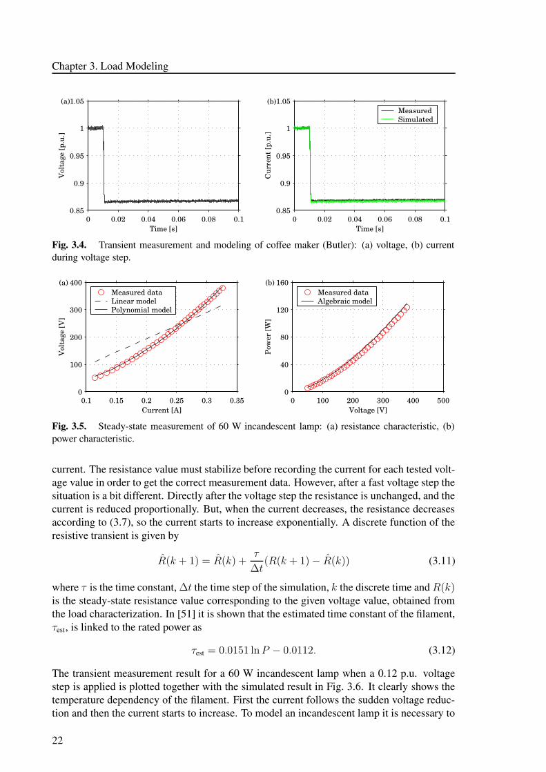
The transient measurements of the heater loads show as expected that a fast reduction ofthe voltage will result in a fast reduction of the current, independently of the magnitude ofthe voltage step. This shows that the model in (3.8) can be used, with R0 calculated fromthe nominal power and R1 = 0. The voltage recorded during the transient measurement isused together with the obtained model parameters to verify the model in PSCAD/EMTDC.The simulated result of the coffee maker model is plotted together with the measurement inFig. 3.4, which shows a 0.12 p.u. voltage step. The simulated current agrees well with themeasured current.
3.3.2 Lighting
A common electric device used for lighting is the incandescent lamp, or light bulb. It con-sists of a filament of tungsten inside a glass bulb filled with argon. Twenty-six incandescentlamps from five different manufacturers, and with five different power ratings, were tested.Also two tungsten halogen lamps were tested. The steady-state measurements for the light-ing loads show that they do not act as a constant resistance load. The term R1 in (3.8) isnot insignificant, i.e., the resistance changes with the current. This means that (3.9) mustbe used to calculate P (U). The measurement result for a 60 W incandescent lamp is shownin Fig. 3.5. The steady-state measurements show that the lighting loads have temperature-dependent resistance and can be modeled as in (3.8). The resistance increases when thecurrent increases, and it can be seen in Fig. 3.5(a) that the voltage increases faster than the
21
Chapter 3. Load Modeling
0 0.02 0.04 0.06 0.08 0.10.85
0.9
0.95
1
1.05
Time [s]
Vol
tage
[p.u
.]
(a)
0 0.02 0.04 0.06 0.08 0.10.85
0.9
0.95
1
1.05
Time [s]
Cur
rent
[p.u
.]
(b)MeasuredSimulated
Fig. 3.4. Transient measurement and modeling of coffee maker (Butler): (a) voltage, (b) currentduring voltage step.
0.1 0.15 0.2 0.25 0.3 0.350
100
200
300
400
Current [A]
Vol
tage
[V]
(a)Measured dataLinear modelPolynomial model
0 100 200 300 400 5000
40
80
120
160
Voltage [V]
Pow
er [W
]
(b)Measured dataAlgebraic model
Fig. 3.5. Steady-state measurement of 60 W incandescent lamp: (a) resistance characteristic, (b)power characteristic.
current. The resistance value must stabilize before recording the current for each tested volt-age value in order to get the correct measurement data. However, after a fast voltage step thesituation is a bit different. Directly after the voltage step the resistance is unchanged, and thecurrent is reduced proportionally. But, when the current decreases, the resistance decreasesaccording to (3.7), so the current starts to increase exponentially. A discrete function of theresistive transient is given by
R(k + 1) = R(k) +τ
∆t(R(k + 1) − R(k)) (3.11)
where τ is the time constant, ∆t the time step of the simulation, k the discrete time and R(k)is the steady-state resistance value corresponding to the given voltage value, obtained fromthe load characterization. In [51] it is shown that the estimated time constant of the filament,τest, is linked to the rated power as
τest = 0.0151 lnP − 0.0112. (3.12)
The transient measurement result for a 60 W incandescent lamp when a 0.12 p.u. voltagestep is applied is plotted together with the simulated result in Fig. 3.6. It clearly shows thetemperature dependency of the filament. First the current follows the sudden voltage reduc-tion and then the current starts to increase. To model an incandescent lamp it is necessary to
22
3.4. Rotating Loads
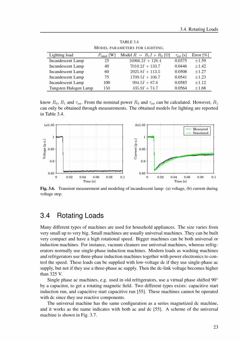
TABLE 3.4MODEL PARAMETERS FOR LIGHTING.
Lighting load Prated [W] Model R = R1I + R0 [Ω] τest [s] Error [%]Incandescent Lamp 25 16966.2I + 128.4 0.0375 ±1.59Incandescent Lamp 40 7010.2I + 133.7 0.0446 ±1.42Incandescent Lamp 60 2925.8I + 113.5 0.0508 ±1.27Incandescent Lamp 75 1709.5I + 106.7 0.0541 ±1.23Incandescent Lamp 100 994.5I + 87.6 0.0585 ±1.12Tungsten Halogen Lamp 150 435.9I + 74.7 0.0564 ±1.68
know R0, R1 and τest. From the nominal power R0 and τest can be calculated. However, R1
can only be obtained through measurements. The obtained models for lighting are reportedin Table 3.4.
0 0.02 0.04 0.06 0.08 0.10.85
0.9
0.95
1
1.05
Time [s]
Vol
tage
[p.u
.]
(a)
0 0.02 0.04 0.06 0.08 0.10.85
0.9
0.95
1
1.05
Time [s]
Cur
rent
[p.u
.]
(b)MeasuredSimulated
Fig. 3.6. Transient measurement and modeling of incandescent lamp: (a) voltage, (b) current duringvoltage step.
3.4 Rotating Loads
Many different types of machines are used for household appliances. The size varies fromvery small up to very big. Small machines are usually universal machines. They can be builtvery compact and have a high rotational speed. Bigger machines can be both universal orinduction machines. For instance, vacuum cleaners use universal machines, whereas refrig-erators normally use single-phase induction machines. Modern loads as washing machinesand refrigerators use three-phase induction machines together with power electronics to con-trol the speed. These loads can be supplied with low-voltage dc if they use single-phase acsupply, but not if they use a three-phase ac supply. Then the dc-link voltage becomes higherthan 325 V.
Single phase ac machines, e.g. used in old refrigerators, use a virtual phase shifted 90°by a capacitor, to get a rotating magnetic field. Two different types exists: capacitive startinduction run, and capacitive start capacitive run [55]. These machines cannot be operatedwith dc since they use reactive components.
The universal machine has the same configuration as a series magnetized dc machine,and it works as the name indicates with both ac and dc [55]. A scheme of the universalmachine is shown in Fig. 3.7.
23

Chapter 3. Load Modeling
(b)
ea
La
Ra Rf
Lf
ua+ -
M
(a)
ua+ -
Fig. 3.7. Series magnetized dc machine: (a) principle scheme, (b) electrical scheme.
The electrical dynamics of the universal machine is given by
ua = ea + Reqia + Leqdia
dt(3.13)
where ua is the applied voltage, ea is the back emf, ia is the current, Req is the equivalentresistance, which is the sum of the resistance of the armature Ra and that of the field windingRf, Leq is the equivalent inductance of the machine, which is the sum of the inductance ofthe armature La and that of the field winding Lf. The back emf, ea, is proportional to therotational speed, ωr, of the machine, which is expressed as [55]
ea = kEωr. (3.14)
The torque of the machine, τe, is proportional to the current, ia, [55]
τe = kTia. (3.15)
The constant kE, equal to kT, is given by the physical design of the machine as
kE = kT =nalr
2aφf(3.16)
where na is the number of conductors on the armature, l is the length of each conductor, ris the radius, a is the cross sectional area of the conductor and φf is the uniform flux in thestator [55]. Since the machine is series magnetized, (3.14) and (3.15) can be rewritten as
ea = keφfωr (3.17)
andτe = ktφfia. (3.18)
The magnetic flux, φf, is directly proportional to the current, which gives
ea = kmiaωr (3.19)
andτe = kmi2a . (3.20)
24
3.4. Rotating Loads
The mechanical dynamics of the machine is given by
Jeqdωr
dt= τe − τl (3.21)
where J is the inertia of the motor, τe is the electric torque and τl is the load torque.The steady-state electrical model of the universal machine is
Ua = Ea + ReqIa = ktφfωr + ReqIa. (3.22)
The steady-state current as a function of the voltage can be found from (3.22) as
Ia =Ua
Req−
ktφfωr
Req. (3.23)
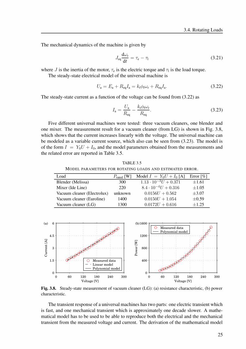
Five different universal machines were tested: three vacuum cleaners, one blender andone mixer. The measurement result for a vacuum cleaner (from LG) is shown in Fig. 3.8,which shows that the current increases linearly with the voltage. The universal machine canbe modeled as a variable current source, which also can be seen from (3.23). The model isof the form I = Y0U + I0, and the model parameters obtained from the measurements andthe related error are reported in Table 3.5.
TABLE 3.5MODEL PARAMETERS FOR ROTATING LOADS AND ESTIMATED ERROR.
Load Prated [W] Model I = Y0U + I0 [A] Error [%]Blender (Melissa) 300 1.13 · 10−3U + 0.371 ±1.61Mixer (Ide Line) 220 8.4 · 10−4U + 0.316 ±1.05Vacuum cleaner (Electrolux) unknown 0.0156U + 0.562 ±3.07Vacuum cleaner (Euroline) 1400 0.0150U + 1.054 ±0.59Vacuum cleaner (LG) 1300 0.0172U + 0.616 ±1.25
0 60 120 180 240 3000
1.5
3
4.5
6
Cur
rent
[A]
Voltage [V]
(a)
Measured dataLinear modelPolynomial model
0 60 120 180 240 3000
400
800
1200
1600
Voltage [V]
Pow
er [W
]
(b)Measured dataPolynomial model
Fig. 3.8. Steady-state measurement of vacuum cleaner (LG): (a) resistance characteristic, (b) powercharacteristic.
The transient response of a universal machines has two parts: one electric transient whichis fast, and one mechanical transient which is approximately one decade slower. A mathe-matical model has to be used to be able to reproduce both the electrical and the mechanicaltransient from the measured voltage and current. The derivation of the mathematical model
25
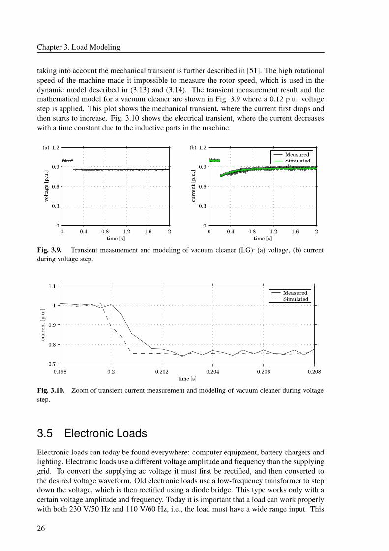
Chapter 3. Load Modeling
taking into account the mechanical transient is further described in [51]. The high rotationalspeed of the machine made it impossible to measure the rotor speed, which is used in thedynamic model described in (3.13) and (3.14). The transient measurement result and themathematical model for a vacuum cleaner are shown in Fig. 3.9 where a 0.12 p.u. voltagestep is applied. This plot shows the mechanical transient, where the current first drops andthen starts to increase. Fig. 3.10 shows the electrical transient, where the current decreaseswith a time constant due to the inductive parts in the machine.
0 0.4 0.8 1.2 1.6 20
0.3
0.6
0.9
1.2
time [s]
volt
age
[p.u
.]
(a)
0 0.4 0.8 1.2 1.6 20
0.3
0.6
0.9
1.2
time [s]
curr
ent
[p.u
.]
(b)MeasuredSimulated
Fig. 3.9. Transient measurement and modeling of vacuum cleaner (LG): (a) voltage, (b) currentduring voltage step.
0.198 0.2 0.202 0.204 0.206 0.2080.7
0.8
0.9
1
1.1
time [s]
curr
ent
[p.u
.]
MeasuredSimulated
Fig. 3.10. Zoom of transient current measurement and modeling of vacuum cleaner during voltagestep.
3.5 Electronic Loads
Electronic loads can today be found everywhere: computer equipment, battery chargers andlighting. Electronic loads use a different voltage amplitude and frequency than the supplyinggrid. To convert the supplying ac voltage it must first be rectified, and then converted tothe desired voltage waveform. Old electronic loads use a low-frequency transformer to stepdown the voltage, which is then rectified using a diode bridge. This type works only with acertain voltage amplitude and frequency. Today it is important that a load can work properlywith both 230 V/50 Hz and 110 V/60 Hz, i.e., the load must have a wide range input. This
26
3.5. Electronic Loads
is accomplished by using a switch mode power supply (SMPS) [46]. The input voltage isfirst rectified by a diode bridge and then adjusted to the load using a dc/dc-converter, whichis shown in Fig. 2.10. The SMPS can be equipped with PFC to decrease the amount of low-frequency current harmonics. All electronic loads with a low-frequency transformer cannotoperate with dc due to the inductance. However, SMPS can be operated with dc without anydesign modifications as long as the dc voltage is in the same range as the ac input. Electronicloads can be divided into two groups with respect to their main function: power supply orlighting appliance.
3.5.1 Power Supply
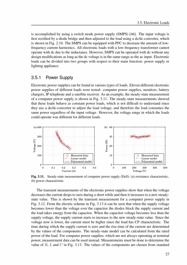
Electronic power supplies can be found in various types of loads. Eleven different electronicpower supplies of different loads were tested: computer power supplies, monitors, batterychargers, IP telephone and a satellite receiver. As an example, the steady-state measurementof a computer power supply is shown in Fig. 3.11. The steady-state measurements showedthat these loads behave as constant power loads, which is not difficult to understand sincethey use a dc/dc-converter to adjust the load voltage, and therefore the load consumes thesame power regardless of the input voltage. However, the voltage range in which the loadscould operate was different for different loads.
0 0.1 0.2 0.3 0.4 0.50
100
200
300
400
Current [A]
Vol
tage
[V]
(a)
Measured dataLinear modelPolynomial model
0 100 200 300 400 5000
15
30
45
60
Voltage [V]
Pow
er [W
]
(b)
Measured dataLinear modelPolynomial model
Fig. 3.11. Steady-state measurement of computer power supply (Dell): (a) resistance characteristic,(b) power characteristic.
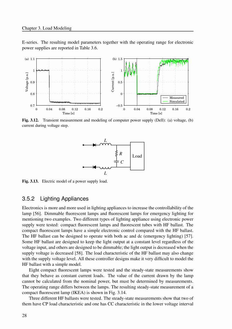
The transient measurements of the electronic power supplies show that when the voltagedecreases the current drops to zero during a short while and then it increases to a new steady-state value. This is shown by the transient measurement for a computer power supply inFig. 3.12. From the electric scheme in Fig. 3.13 it can be seen that when the supply voltagebecomes lower than the voltage over the capacitor the diodes block the supply current andthe load takes energy from the capacitor. When the capacitor voltage becomes less than thesupply voltage, the supply current starts to increase to the new steady-state value. Since thevoltage now is lower, the current must be higher since the load has CP characteristic. Thetime during which the supply current is zero and the rise time of the current are determinedby the values of the components. The steady-state model can be calculated from the ratedpower of the load. For computer power supplies, which are not always operating at nominalpower, measurement data can be used instead. Measurements must be done to determine thevalue of R, L and C in Fig. 3.13. The values of the components are chosen from standard
27
Chapter 3. Load Modeling
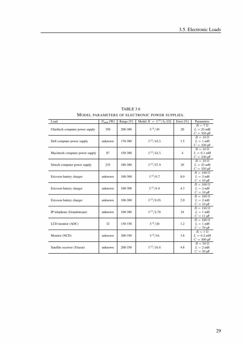
E-series. The resulting model parameters together with the operating range for electronicpower supplies are reported in Table 3.6.
0 0.04 0.08 0.12 0.16 0.20.7
0.8
0.9
1
1.1
Time [s]
Vol
tage
[p.u
.]
(a)
0 0.04 0.08 0.12 0.16 0.2−0.5
0
0.5
1
1.5
Time [s]C
urre
nt [p
.u.]
(b)
MeasuredSimulated
Fig. 3.12. Transient measurement and modeling of computer power supply (Dell): (a) voltage, (b)current during voltage step.
L
R Load
L
C
Fig. 3.13. Electric model of a power supply load.
3.5.2 Lighting Appliances
Electronics is more and more used in lighting appliances to increase the controllability of thelamp [56]. Dimmable fluorescent lamps and fluorescent lamps for emergency lighting formentioning two examples. Two different types of lighting appliance using electronic powersupply were tested: compact fluorescent lamps and fluorescent tubes with HF ballast. Thecompact fluorescent lamps have a simple electronic control compared with the HF ballast.The HF ballast can be designed to operate with both ac and dc (emergency lighting) [57].Some HF ballast are designed to keep the light output at a constant level regardless of thevoltage input, and others are designed to be dimmable; the light output is decreased when thesupply voltage is decreased [58]. The load characteristic of the HF ballast may also changewith the supply voltage level. All these controller designs make it very difficult to model theHF ballast with a simple model.
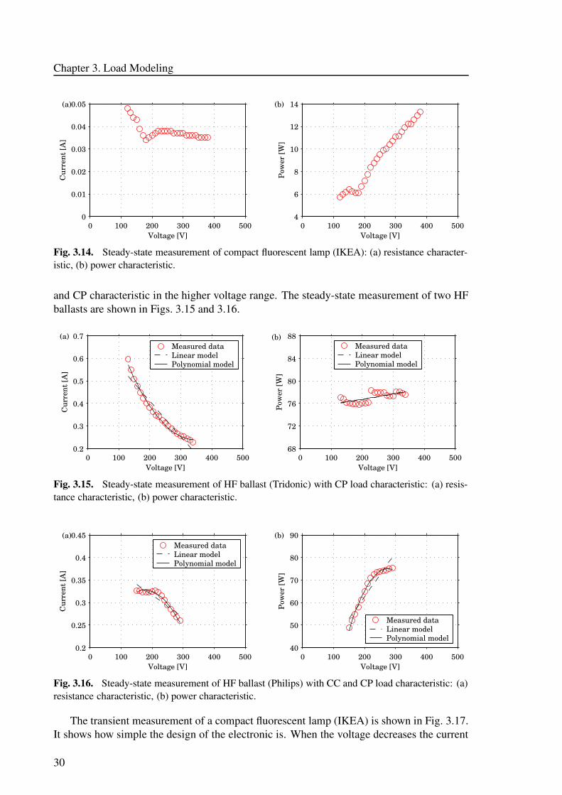
Eight compact fluorescent lamps were tested and the steady-state measurements showthat they behave as constant current loads. The value of the current drawn by the lampcannot be calculated from the nominal power, but must be determined by measurements.The operating range differs between the lamps. The resulting steady-state measurement of acompact fluorescent lamp (IKEA) is shown in Fig. 3.14.
Three different HF ballasts were tested. The steady-state measurements show that two ofthem have CP load characteristic and one has CC characteristic in the lower voltage interval
28
3.5. Electronic Loads
TABLE 3.6MODEL PARAMETERS OF ELECTRONIC POWER SUPPLIES.
Load Prated [W] Range [V] Model R = U2/I0 [Ω] Error [%] Parameters
Chieftech computer power supply 350 200-380 U2/40 20R = 7 Ω
L = 25 mHC = 350 µF
Dell computer power supply unknown 170-380 U2/43.5 1.5R = 10 Ω
L = 1 mHC = 230 µF
Macintosh computer power supply 87 150-380 U2/43.5 4R = 10 Ω
L = 0.1 mHC = 230 µF
Sirtech computer power supply 235 180-380 U2/37.9 20R = 10 Ω
L = 25 mHC = 350 µF
Ericsson battery charger unknown 100-300 U2/6.7 8.0R = 100 Ω
L = 2 mHC = 10 µF
Ericsson battery charger unknown 100-300 U2/6.9 4.3R = 100 Ω
L = 2 mHC = 10 µF
Ericsson battery charger unknown 100-300 U2/8.05 2.0R = 100 Ω
L = 2 mHC = 10 µF
IP telephone (Grandstream) unknown 100-380 U2/2.76 24R = 150 Ω
L = 1 mHC = 11 µF
LCD monitor (AOC) 32 130-330 U2/30 1.2R = 100 Ω
L = 1 mHC = 70 µF
Monitor (NCD) unknown 200-350 U2/84 3.8R = 1 Ω
L = 0.2 mHC = 300 µF
Satellite receiver (Triasat) unknown 200-350 U2/16.6 4.8R = 50 Ω
L = 2 mHC = 50 µF
29
Chapter 3. Load Modeling
0 100 200 300 400 5000
0.01
0.02
0.03
0.04
0.05
Cur
rent
[A]
Voltage [V]
(a)
0 100 200 300 400 5004
6
8
10
12
14
Voltage [V]
Pow
er [W
]
(b)
Fig. 3.14. Steady-state measurement of compact fluorescent lamp (IKEA): (a) resistance character-istic, (b) power characteristic.
and CP characteristic in the higher voltage range. The steady-state measurement of two HFballasts are shown in Figs. 3.15 and 3.16.
0 100 200 300 400 5000.2
0.3
0.4
0.5
0.6
0.7
Cur
rent
[A]
Voltage [V]
(a)Measured dataLinear modelPolynomial model
0 100 200 300 400 50068
72
76
80
84
88
Voltage [V]
Pow
er [W
]
(b)Measured dataLinear modelPolynomial model
Fig. 3.15. Steady-state measurement of HF ballast (Tridonic) with CP load characteristic: (a) resis-tance characteristic, (b) power characteristic.
0 100 200 300 400 5000.2
0.25
0.3
0.35
0.4
0.45
Cur
rent
[A]
Voltage [V]
(a)Measured dataLinear modelPolynomial model
0 100 200 300 400 50040
50
60
70
80
90
Voltage [V]
Pow
er [W
]
(b)
Measured dataLinear modelPolynomial model
Fig. 3.16. Steady-state measurement of HF ballast (Philips) with CC and CP load characteristic: (a)resistance characteristic, (b) power characteristic.
The transient measurement of a compact fluorescent lamp (IKEA) is shown in Fig. 3.17.It shows how simple the design of the electronic is. When the voltage decreases the current
30
3.5. Electronic Loads
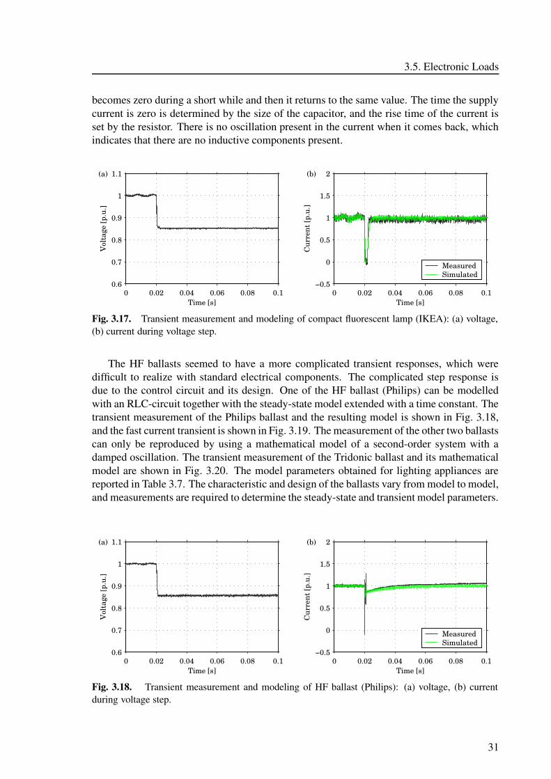
becomes zero during a short while and then it returns to the same value. The time the supplycurrent is zero is determined by the size of the capacitor, and the rise time of the current isset by the resistor. There is no oscillation present in the current when it comes back, whichindicates that there are no inductive components present.
0 0.02 0.04 0.06 0.08 0.10.6
0.7
0.8
0.9
1
1.1
Time [s]
Vol
tage
[p.u
.]
(a)
0 0.02 0.04 0.06 0.08 0.1−0.5
0
0.5
1
1.5
2
Time [s]C
urre
nt [p
.u.]
(b)
MeasuredSimulated
Fig. 3.17. Transient measurement and modeling of compact fluorescent lamp (IKEA): (a) voltage,(b) current during voltage step.
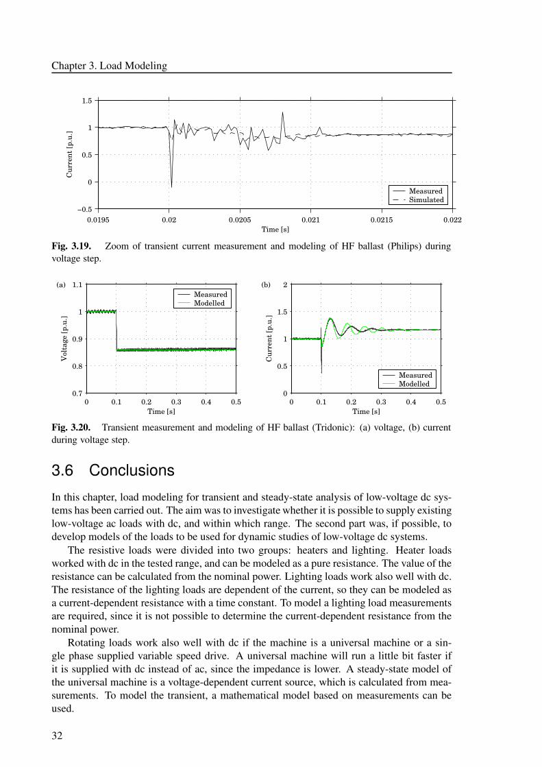
The HF ballasts seemed to have a more complicated transient responses, which weredifficult to realize with standard electrical components. The complicated step response isdue to the control circuit and its design. One of the HF ballast (Philips) can be modelledwith an RLC-circuit together with the steady-state model extended with a time constant. Thetransient measurement of the Philips ballast and the resulting model is shown in Fig. 3.18,and the fast current transient is shown in Fig. 3.19. The measurement of the other two ballastscan only be reproduced by using a mathematical model of a second-order system with adamped oscillation. The transient measurement of the Tridonic ballast and its mathematicalmodel are shown in Fig. 3.20. The model parameters obtained for lighting appliances arereported in Table 3.7. The characteristic and design of the ballasts vary from model to model,and measurements are required to determine the steady-state and transient model parameters.
0 0.02 0.04 0.06 0.08 0.10.6
0.7
0.8
0.9
1
1.1
Time [s]
Vol
tage
[p.u
.]
(a)
0 0.02 0.04 0.06 0.08 0.1−0.5
0
0.5
1
1.5
2
Time [s]
Cur
rent
[p.u
.]
(b)
MeasuredSimulated
Fig. 3.18. Transient measurement and modeling of HF ballast (Philips): (a) voltage, (b) currentduring voltage step.
31
Chapter 3. Load Modeling
0.0195 0.02 0.0205 0.021 0.0215 0.022−0.5
0
0.5
1
1.5
Time [s]
Cur
rent
[p.u
.]
MeasuredSimulated
Fig. 3.19. Zoom of transient current measurement and modeling of HF ballast (Philips) duringvoltage step.
0 0.1 0.2 0.3 0.4 0.50.7
0.8
0.9
1
1.1(a)
Time [s]
Vol
tage
[p.u
.]
MeasuredModelled
0 0.1 0.2 0.3 0.4 0.50
0.5
1
1.5
2(b)
Time [s]
Cur
rent
[p.u
.]
MeasuredModelled
Fig. 3.20. Transient measurement and modeling of HF ballast (Tridonic): (a) voltage, (b) currentduring voltage step.
3.6 Conclusions
In this chapter, load modeling for transient and steady-state analysis of low-voltage dc sys-tems has been carried out. The aim was to investigate whether it is possible to supply existinglow-voltage ac loads with dc, and within which range. The second part was, if possible, todevelop models of the loads to be used for dynamic studies of low-voltage dc systems.
The resistive loads were divided into two groups: heaters and lighting. Heater loadsworked with dc in the tested range, and can be modeled as a pure resistance. The value of theresistance can be calculated from the nominal power. Lighting loads work also well with dc.The resistance of the lighting loads are dependent of the current, so they can be modeled asa current-dependent resistance with a time constant. To model a lighting load measurementsare required, since it is not possible to determine the current-dependent resistance from thenominal power.
Rotating loads work also well with dc if the machine is a universal machine or a sin-gle phase supplied variable speed drive. A universal machine will run a little bit faster ifit is supplied with dc instead of ac, since the impedance is lower. A steady-state model ofthe universal machine is a voltage-dependent current source, which is calculated from mea-surements. To model the transient, a mathematical model based on measurements can beused.
32
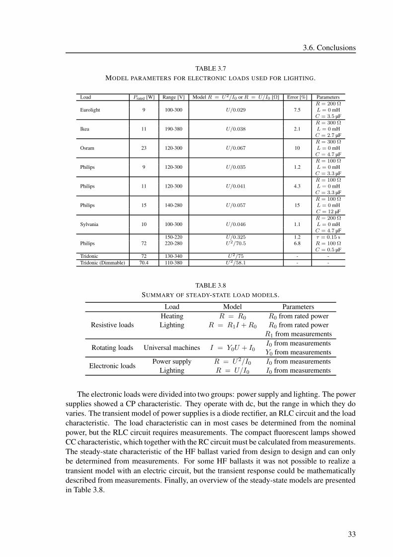
3.6. Conclusions
TABLE 3.7MODEL PARAMETERS FOR ELECTRONIC LOADS USED FOR LIGHTING.
Load Prated [W] Range [V] Model R = U2/I0 or R = U/I0 [Ω] Error [%] Parameters
Eurolight 9 100-300 U/0.029 7.5R = 200 Ω
L = 0 mHC = 3.5 µF
Ikea 11 190-380 U/0.038 2.1R = 300 Ω
L = 0 mHC = 2.7 µF
Osram 23 120-300 U/0.067 10R = 300 Ω
L = 0 mHC = 4.7 µF
Philips 9 120-300 U/0.035 1.2R = 100 Ω
L = 0 mHC = 3.3 µF
Philips 11 120-300 U/0.041 4.3R = 100 Ω
L = 0 mHC = 3.3 µF
Philips 15 140-280 U/0.057 15R = 100 Ω
L = 0 mHC = 12 µF
Sylvania 10 100-300 U/0.046 1.1R = 200 Ω
L = 0 mHC = 4.7 µF
Philips 72150-220 U/0.325 1.2 τ = 0.15 s220-280 U2/70.5 6.8 R = 100 Ω
C = 0.5 µFTridonic 72 130-340 U2/75 - -Tridonic (Dimmable) 70.4 110-380 U2/58.1 - -
TABLE 3.8SUMMARY OF STEADY-STATE LOAD MODELS.
Load Model Parameters
Resistive loadsHeating R = R0 R0 from rated powerLighting R = R1I + R0 R0 from rated power
R1 from measurements
Rotating loads Universal machines I = Y0U + I0
I0 from measurementsY0 from measurements
Electronic loadsPower supply R = U 2/I0 I0 from measurements
Lighting R = U/I0 I0 from measurements
The electronic loads were divided into two groups: power supply and lighting. The powersupplies showed a CP characteristic. They operate with dc, but the range in which they dovaries. The transient model of power supplies is a diode rectifier, an RLC circuit and the loadcharacteristic. The load characteristic can in most cases be determined from the nominalpower, but the RLC circuit requires measurements. The compact fluorescent lamps showedCC characteristic, which together with the RC circuit must be calculated from measurements.The steady-state characteristic of the HF ballast varied from design to design and can onlybe determined from measurements. For some HF ballasts it was not possible to realize atransient model with an electric circuit, but the transient response could be mathematicallydescribed from measurements. Finally, an overview of the steady-state models are presentedin Table 3.8.
33

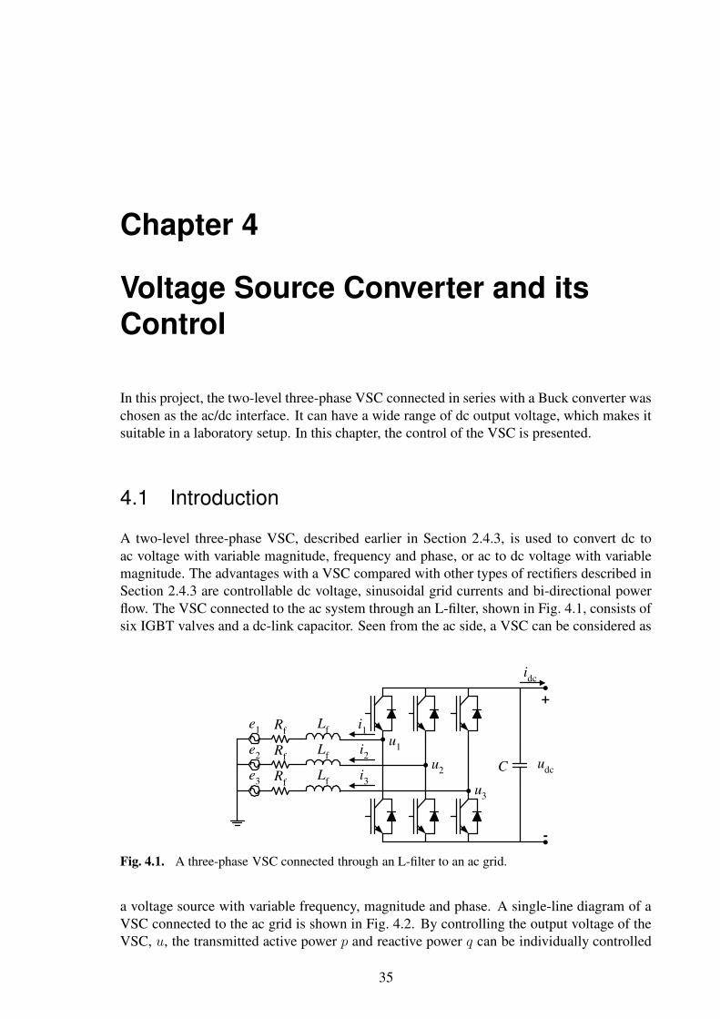
Chapter 4
Voltage Source Converter and itsControl
In this project, the two-level three-phase VSC connected in series with a Buck converter waschosen as the ac/dc interface. It can have a wide range of dc output voltage, which makes itsuitable in a laboratory setup. In this chapter, the control of the VSC is presented.
4.1 Introduction
A two-level three-phase VSC, described earlier in Section 2.4.3, is used to convert dc toac voltage with variable magnitude, frequency and phase, or ac to dc voltage with variablemagnitude. The advantages with a VSC compared with other types of rectifiers described inSection 2.4.3 are controllable dc voltage, sinusoidal grid currents and bi-directional powerflow. The VSC connected to the ac system through an L-filter, shown in Fig. 4.1, consists ofsix IGBT valves and a dc-link capacitor. Seen from the ac side, a VSC can be considered as
udc
e1
+
-
LfRf
e2 LfRf
e3 LfRf
u1
u2
u3
i1i2
i3
idc
C
Fig. 4.1. A three-phase VSC connected through an L-filter to an ac grid.
a voltage source with variable frequency, magnitude and phase. A single-line diagram of aVSC connected to the ac grid is shown in Fig. 4.2. By controlling the output voltage of theVSC, u, the transmitted active power p and reactive power q can be individually controlled
35
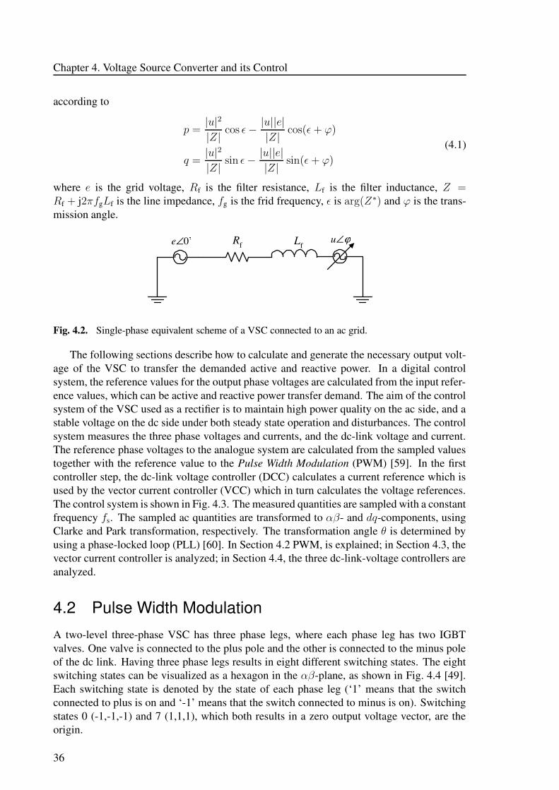
Chapter 4. Voltage Source Converter and its Control
according to
p =|u|2
|Z|cos ε −
|u||e|
|Z|cos(ε + ϕ)
q =|u|2
|Z|sin ε −
|u||e|
|Z|sin(ε + ϕ)
(4.1)
where e is the grid voltage, Rf is the filter resistance, Lf is the filter inductance, Z =Rf + j2πfgLf is the line impedance, fg is the frid frequency, ε is arg(Z∗) and ϕ is the trans-mission angle.
LfRf
0∠e ϕ∠u
Fig. 4.2. Single-phase equivalent scheme of a VSC connected to an ac grid.
The following sections describe how to calculate and generate the necessary output volt-age of the VSC to transfer the demanded active and reactive power. In a digital controlsystem, the reference values for the output phase voltages are calculated from the input refer-ence values, which can be active and reactive power transfer demand. The aim of the controlsystem of the VSC used as a rectifier is to maintain high power quality on the ac side, and astable voltage on the dc side under both steady state operation and disturbances. The controlsystem measures the three phase voltages and currents, and the dc-link voltage and current.The reference phase voltages to the analogue system are calculated from the sampled valuestogether with the reference value to the Pulse Width Modulation (PWM) [59]. In the firstcontroller step, the dc-link voltage controller (DCC) calculates a current reference which isused by the vector current controller (VCC) which in turn calculates the voltage references.The control system is shown in Fig. 4.3. The measured quantities are sampled with a constantfrequency fs. The sampled ac quantities are transformed to αβ- and dq-components, usingClarke and Park transformation, respectively. The transformation angle θ is determined byusing a phase-locked loop (PLL) [60]. In Section 4.2 PWM, is explained; in Section 4.3, thevector current controller is analyzed; in Section 4.4, the three dc-link-voltage controllers areanalyzed.
4.2 Pulse Width Modulation
A two-level three-phase VSC has three phase legs, where each phase leg has two IGBTvalves. One valve is connected to the plus pole and the other is connected to the minus poleof the dc link. Having three phase legs results in eight different switching states. The eightswitching states can be visualized as a hexagon in the αβ-plane, as shown in Fig. 4.4 [49].Each switching state is denoted by the state of each phase leg (‘1’ means that the switchconnected to plus is on and ‘-1’ means that the switch connected to minus is on). Switchingstates 0 (-1,-1,-1) and 7 (1,1,1), which both results in a zero output voltage vector, are theorigin.
36

4.2. Pulse Width Modulation
udcidc
S/H
S/H
S/H
123αβ
123αβ
PLL
αβdq
αβdq
θ
θ
DCC
VCC
e1e2e3
i1i2i3
PWMdqαβ
αβ123
θ + ∆θ
Firingsignalsto VSC
refαβu
dqe
refqi
dqi
αβe
αβi
Fig. 4.3. Block scheme of VSC control system.
α
β
s = 1
s = 6s = 4
s = 3
s = 5
s = 2
u1 (1,-1,-1)
u2 (1,1,-1)u3 (-1,1,-1)
u4 (-1,1,1)
u5 (-1,-1,1) u6 (1,-1,1)
u7u0
Fig. 4.4. The eight switching states of a two-level three-phase VSC.
37
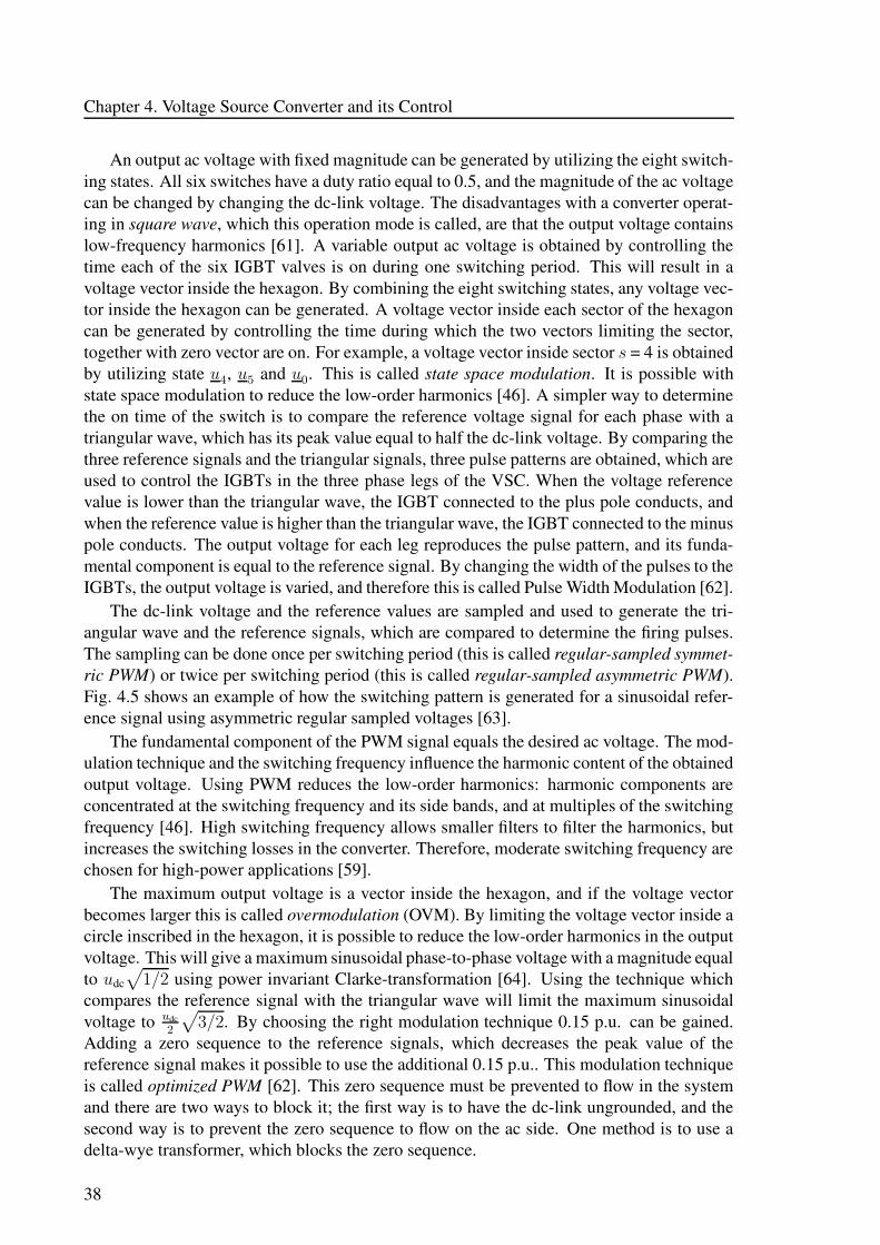
Chapter 4. Voltage Source Converter and its Control
An output ac voltage with fixed magnitude can be generated by utilizing the eight switch-ing states. All six switches have a duty ratio equal to 0.5, and the magnitude of the ac voltagecan be changed by changing the dc-link voltage. The disadvantages with a converter operat-ing in square wave, which this operation mode is called, are that the output voltage containslow-frequency harmonics [61]. A variable output ac voltage is obtained by controlling thetime each of the six IGBT valves is on during one switching period. This will result in avoltage vector inside the hexagon. By combining the eight switching states, any voltage vec-tor inside the hexagon can be generated. A voltage vector inside each sector of the hexagoncan be generated by controlling the time during which the two vectors limiting the sector,together with zero vector are on. For example, a voltage vector inside sector s = 4 is obtainedby utilizing state u4, u5 and u0. This is called state space modulation. It is possible withstate space modulation to reduce the low-order harmonics [46]. A simpler way to determinethe on time of the switch is to compare the reference voltage signal for each phase with atriangular wave, which has its peak value equal to half the dc-link voltage. By comparing thethree reference signals and the triangular signals, three pulse patterns are obtained, which areused to control the IGBTs in the three phase legs of the VSC. When the voltage referencevalue is lower than the triangular wave, the IGBT connected to the plus pole conducts, andwhen the reference value is higher than the triangular wave, the IGBT connected to the minuspole conducts. The output voltage for each leg reproduces the pulse pattern, and its funda-mental component is equal to the reference signal. By changing the width of the pulses to theIGBTs, the output voltage is varied, and therefore this is called Pulse Width Modulation [62].
The dc-link voltage and the reference values are sampled and used to generate the tri-angular wave and the reference signals, which are compared to determine the firing pulses.The sampling can be done once per switching period (this is called regular-sampled symmet-ric PWM) or twice per switching period (this is called regular-sampled asymmetric PWM).Fig. 4.5 shows an example of how the switching pattern is generated for a sinusoidal refer-ence signal using asymmetric regular sampled voltages [63].
The fundamental component of the PWM signal equals the desired ac voltage. The mod-ulation technique and the switching frequency influence the harmonic content of the obtainedoutput voltage. Using PWM reduces the low-order harmonics: harmonic components areconcentrated at the switching frequency and its side bands, and at multiples of the switchingfrequency [46]. High switching frequency allows smaller filters to filter the harmonics, butincreases the switching losses in the converter. Therefore, moderate switching frequency arechosen for high-power applications [59].
The maximum output voltage is a vector inside the hexagon, and if the voltage vectorbecomes larger this is called overmodulation (OVM). By limiting the voltage vector inside acircle inscribed in the hexagon, it is possible to reduce the low-order harmonics in the outputvoltage. This will give a maximum sinusoidal phase-to-phase voltage with a magnitude equalto udc
√
1/2 using power invariant Clarke-transformation [64]. Using the technique whichcompares the reference signal with the triangular wave will limit the maximum sinusoidalvoltage to udc
2
√
3/2. By choosing the right modulation technique 0.15 p.u. can be gained.Adding a zero sequence to the reference signals, which decreases the peak value of thereference signal makes it possible to use the additional 0.15 p.u.. This modulation techniqueis called optimized PWM [62]. This zero sequence must be prevented to flow in the systemand there are two ways to block it; the first way is to have the dc-link ungrounded, and thesecond way is to prevent the zero sequence to flow on the ac side. One method is to use adelta-wye transformer, which blocks the zero sequence.
38
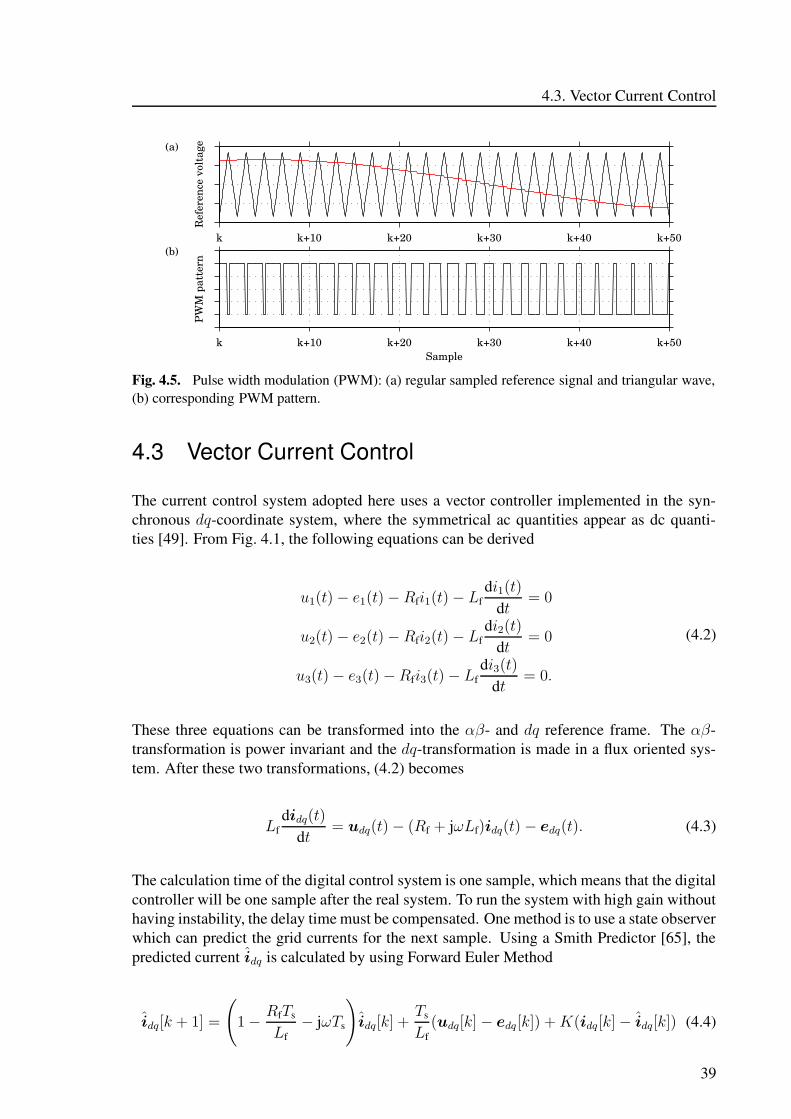
4.3. Vector Current Control
k k+10 k+20 k+30 k+40 k+50
Ref
eren
ce v
olta
ge(a)
k k+10 k+20 k+30 k+40 k+50
PW
M p
atte
rn
Sample
(b)
Fig. 4.5. Pulse width modulation (PWM): (a) regular sampled reference signal and triangular wave,(b) corresponding PWM pattern.
4.3 Vector Current Control
The current control system adopted here uses a vector controller implemented in the syn-chronous dq-coordinate system, where the symmetrical ac quantities appear as dc quanti-ties [49]. From Fig. 4.1, the following equations can be derived
u1(t) − e1(t) − Rfi1(t) − Lfdi1(t)
dt= 0
u2(t) − e2(t) − Rfi2(t) − Lfdi2(t)
dt= 0
u3(t) − e3(t) − Rfi3(t) − Lfdi3(t)
dt= 0.
(4.2)
These three equations can be transformed into the αβ- and dq reference frame. The αβ-transformation is power invariant and the dq-transformation is made in a flux oriented sys-tem. After these two transformations, (4.2) becomes
Lfdidq(t)
dt= udq(t) − (Rf + jωLf)idq(t) − edq(t). (4.3)
The calculation time of the digital control system is one sample, which means that the digitalcontroller will be one sample after the real system. To run the system with high gain withouthaving instability, the delay time must be compensated. One method is to use a state observerwhich can predict the grid currents for the next sample. Using a Smith Predictor [65], thepredicted current idq is calculated by using Forward Euler Method
idq[k + 1] =
(
1 −RfTs
Lf− jωTs
)
idq[k] +Ts
Lf(udq[k] − edq[k]) + K(idq[k] − idq[k]) (4.4)
39
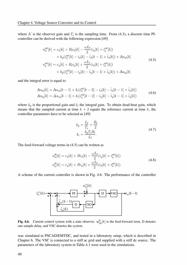
Chapter 4. Voltage Source Converter and its Control
where K is the observer gain and Ts is the sampling time. From (4.3), a discrete time PI-controller can be derived with the following expression [49]
urefd [k] = ed[k] + Rfid[k] −
ωLf
2(iq[k] + iref
q [k])
+ kp(irefd [k] − id[k] − id[k − 1] + id[k]) + ∆uid[k]
urefq [k] = eq[k] + Rfiq[k] +
ωLf
2(id[k] + iref
d [k])
+ kp(irefq [k] − iq[k] − iq[k − 1] + iq[k]) + ∆uiq[k]
(4.5)
and the integral error is equal to
∆uid[k] = ∆uid[k − 1] + ki(irefd [k − 2] − id[k] − id[k − 1] + id[k])
∆uiq[k] = ∆uiq[k − 1] + ki(irefq [k − 2] − iq[k] − iq[k − 1] + iq[k])
(4.6)
where kp is the proportional gain and ki the integral gain. To obtain dead-beat gain, whichmeans that the sampled current at time k + 2 equals the reference current at time k, thecontroller parameters have to be selected as [49]
kp =Lf
Ts+
Rf
2
ki =kpTsRf
Lf.
(4.7)
The feed-forward voltage terms in (4.5) can be written as
uffd [k] = ed[k] + Rid[k] −
ωLf
2(iq[k] + iref
q [k])
uffq [k] = eq[k] + Riq[k] +
ωLf
2(id[k] + iref
d [k]).
(4.8)
A scheme of the current controller is shown in Fig. 4.6. The performance of the controller
PI
D SO
VSC+
++
+-
-- +][kiref
dq ]1[ −kidq
][ku ffdq
][ˆ kidq
]1[ˆ −kidq
D
Fig. 4.6. Current control system with a state observer. uffdq[k] is the feed-forward term, D denotes
one sample delay, and VSC denotes the system.
was simulated in PSCAD/EMTDC, and tested in a laboratory setup, which is described inChapter 6. The VSC is connected to a stiff ac grid and supplied with a stiff dc source. Theparameters of the laboratory system in Table 4.1 were used in the simulations.
40
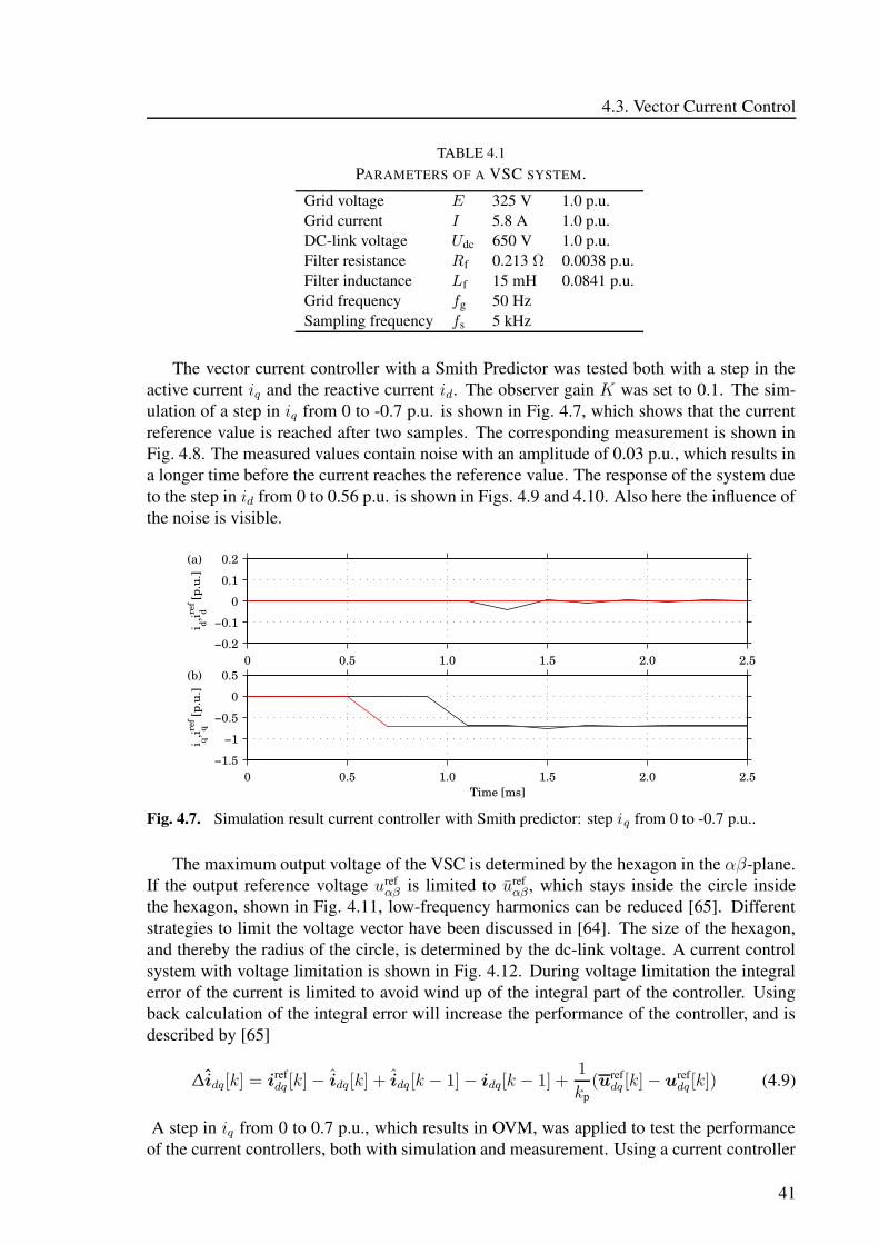
4.3. Vector Current Control
TABLE 4.1PARAMETERS OF A VSC SYSTEM.
Grid voltage E 325 V 1.0 p.u.Grid current I 5.8 A 1.0 p.u.DC-link voltage Udc 650 V 1.0 p.u.Filter resistance Rf 0.213 Ω 0.0038 p.u.Filter inductance Lf 15 mH 0.0841 p.u.Grid frequency fg 50 HzSampling frequency fs 5 kHz
The vector current controller with a Smith Predictor was tested both with a step in theactive current iq and the reactive current id. The observer gain K was set to 0.1. The sim-ulation of a step in iq from 0 to -0.7 p.u. is shown in Fig. 4.7, which shows that the currentreference value is reached after two samples. The corresponding measurement is shown inFig. 4.8. The measured values contain noise with an amplitude of 0.03 p.u., which results ina longer time before the current reaches the reference value. The response of the system dueto the step in id from 0 to 0.56 p.u. is shown in Figs. 4.9 and 4.10. Also here the influence ofthe noise is visible.
0 0.5 1.0 1.5 2.0 2.5−0.2
−0.1
0
0.1
0.2
i d,i dref [p
.u.]
(a)
0 0.5 1.0 1.5 2.0 2.5−1.5
−1
−0.5
0
0.5
i q,i qref [p
.u.]
(b)
Time [ms]
Fig. 4.7. Simulation result current controller with Smith predictor: step iq from 0 to -0.7 p.u..
The maximum output voltage of the VSC is determined by the hexagon in the αβ-plane.If the output reference voltage uref
αβ is limited to urefαβ, which stays inside the circle inside
the hexagon, shown in Fig. 4.11, low-frequency harmonics can be reduced [65]. Differentstrategies to limit the voltage vector have been discussed in [64]. The size of the hexagon,and thereby the radius of the circle, is determined by the dc-link voltage. A current controlsystem with voltage limitation is shown in Fig. 4.12. During voltage limitation the integralerror of the current is limited to avoid wind up of the integral part of the controller. Usingback calculation of the integral error will increase the performance of the controller, and isdescribed by [65]
∆idq[k] = irefdq [k] − idq[k] + idq[k − 1] − idq[k − 1] +
1
kp(uref
dq [k] − urefdq [k]) (4.9)
A step in iq from 0 to 0.7 p.u., which results in OVM, was applied to test the performanceof the current controllers, both with simulation and measurement. Using a current controller
41
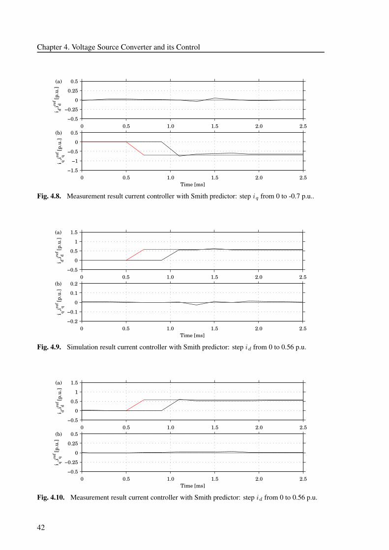
Chapter 4. Voltage Source Converter and its Control
0 0.5 1.0 1.5 2.0 2.5−0.5
−0.25
0
0.25
0.5
i d,i dref [p
.u.]
(a)
0 0.5 1.0 1.5 2.0 2.5−1.5
−1
−0.5
0
0.5
i q,i qref [p
.u.]
(b)
Time [ms]
Fig. 4.8. Measurement result current controller with Smith predictor: step iq from 0 to -0.7 p.u..
0 0.5 1.0 1.5 2.0 2.5−0.5
0
0.5
1
1.5
i d,i dref [p
.u.]
(a)
0 0.5 1.0 1.5 2.0 2.5−0.2
−0.1
0
0.1
0.2
i q,i qref [p
.u.]
(b)
Time [ms]
Fig. 4.9. Simulation result current controller with Smith predictor: step id from 0 to 0.56 p.u.
0 0.5 1.0 1.5 2.0 2.5−0.5
0
0.5
1
1.5
i d,i dref [p
.u.]
(a)
0 0.5 1.0 1.5 2.0 2.5−0.5
−0.25
0
0.25
0.5
i q,i qref [p
.u.]
(b)
Time [ms]
Fig. 4.10. Measurement result current controller with Smith predictor: step id from 0 to 0.56 p.u.
42
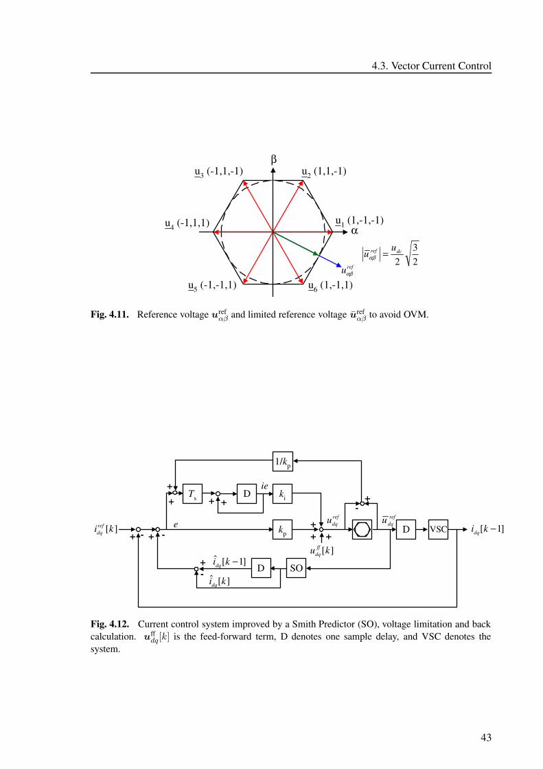
4.3. Vector Current Control
α
β
u1 (1,-1,-1)
u2 (1,1,-1)u3 (-1,1,-1)
u4 (-1,1,1)
u5 (-1,-1,1) u6 (1,-1,1)
refuαβ
23
2dcref u
u =αβ
Fig. 4.11. Reference voltage urefαβ and limited reference voltage u
refαβ to avoid OVM.
VSC+
SO
1/kp
D kiTs
kp-
++
+ +
++
-+
refdqu
ie
e+
][kirefdq D
D+-
-
]1[ˆ −kidq
refdqu
][ˆ kidq
]1[ −kidq
][ku ffdq
+
Fig. 4.12. Current control system improved by a Smith Predictor (SO), voltage limitation and backcalculation. u
ffdq[k] is the feed-forward term, D denotes one sample delay, and VSC denotes the
system.
43
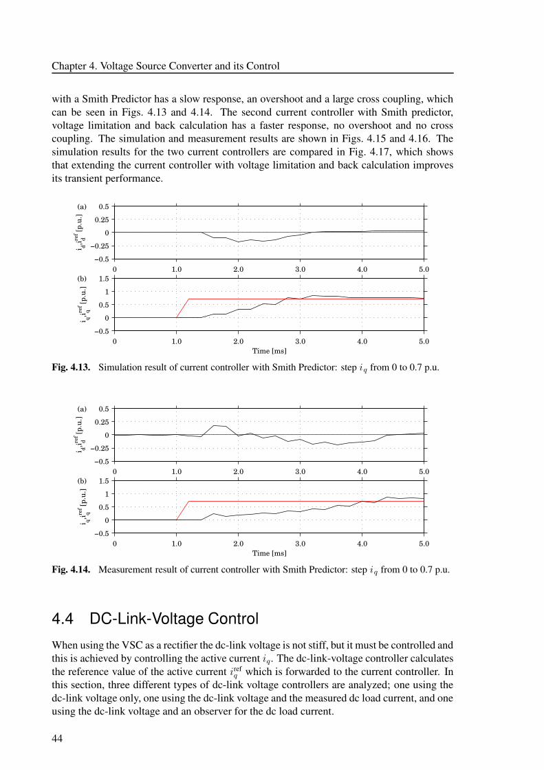
Chapter 4. Voltage Source Converter and its Control
with a Smith Predictor has a slow response, an overshoot and a large cross coupling, whichcan be seen in Figs. 4.13 and 4.14. The second current controller with Smith predictor,voltage limitation and back calculation has a faster response, no overshoot and no crosscoupling. The simulation and measurement results are shown in Figs. 4.15 and 4.16. Thesimulation results for the two current controllers are compared in Fig. 4.17, which showsthat extending the current controller with voltage limitation and back calculation improvesits transient performance.
0 1.0 2.0 3.0 4.0 5.0−0.5
−0.25
0
0.25
0.5
i d,i dref [p
.u.]
(a)
0 1.0 2.0 3.0 4.0 5.0−0.5
0
0.5
1
1.5
i q,i qref [p
.u.]
(b)
Time [ms]
Fig. 4.13. Simulation result of current controller with Smith Predictor: step iq from 0 to 0.7 p.u.
0 1.0 2.0 3.0 4.0 5.0−0.5
−0.25
0
0.25
0.5
i d,i dref [p
.u.]
(a)
0 1.0 2.0 3.0 4.0 5.0−0.5
0
0.5
1
1.5
i q,i qref [p
.u.]
(b)
Time [ms]
Fig. 4.14. Measurement result of current controller with Smith Predictor: step iq from 0 to 0.7 p.u.
4.4 DC-Link-Voltage Control
When using the VSC as a rectifier the dc-link voltage is not stiff, but it must be controlled andthis is achieved by controlling the active current iq. The dc-link-voltage controller calculatesthe reference value of the active current iref
q which is forwarded to the current controller. Inthis section, three different types of dc-link voltage controllers are analyzed; one using thedc-link voltage only, one using the dc-link voltage and the measured dc load current, and oneusing the dc-link voltage and an observer for the dc load current.
44

4.4. DC-Link-Voltage Control
0 1.0 2.0 3.0 4.0 5.0−0.5
−0.25
0
0.25
0.5i d,i dre
f [p.u
.](a)
0 1.0 2.0 3.0 4.0 5.0−0.5
0
0.5
1
1.5
i q,i qref [p
.u.]
(b)
Time [ms]
Fig. 4.15. Simulation result of current controller with Smith predictor, voltage limitation and backcalculation: step iq from 0 to 0.7 p.u.
0 1.0 2.0 3.0 4.0 5.0−0.5
−0.25
0
0.25
0.5
i d,i dref [p
.u.]
(a)
0 1.0 2.0 3.0 4.0 5.0−0.5
0
0.5
1
1.5
i q,i qref [p
.u.]
(b)
Time [ms]
Fig. 4.16. Measurement result of current controller with Smith Predictor, voltage limitation andback calculation: step iq from 0 to 0.7 p.u.
0 2.0 4.0 6.0 8.0 10.00
0.1
0.2
0.3
0.4
0.5
0.6
0.7
0.8
0.9
i q,i qref [p
.u.]
Time [ms]
Fig. 4.17. Simulation result for current controller with Smith Predictor (solid) and current controllerwith Smith Predictor, voltage limitation and back calculation (dashed).
45
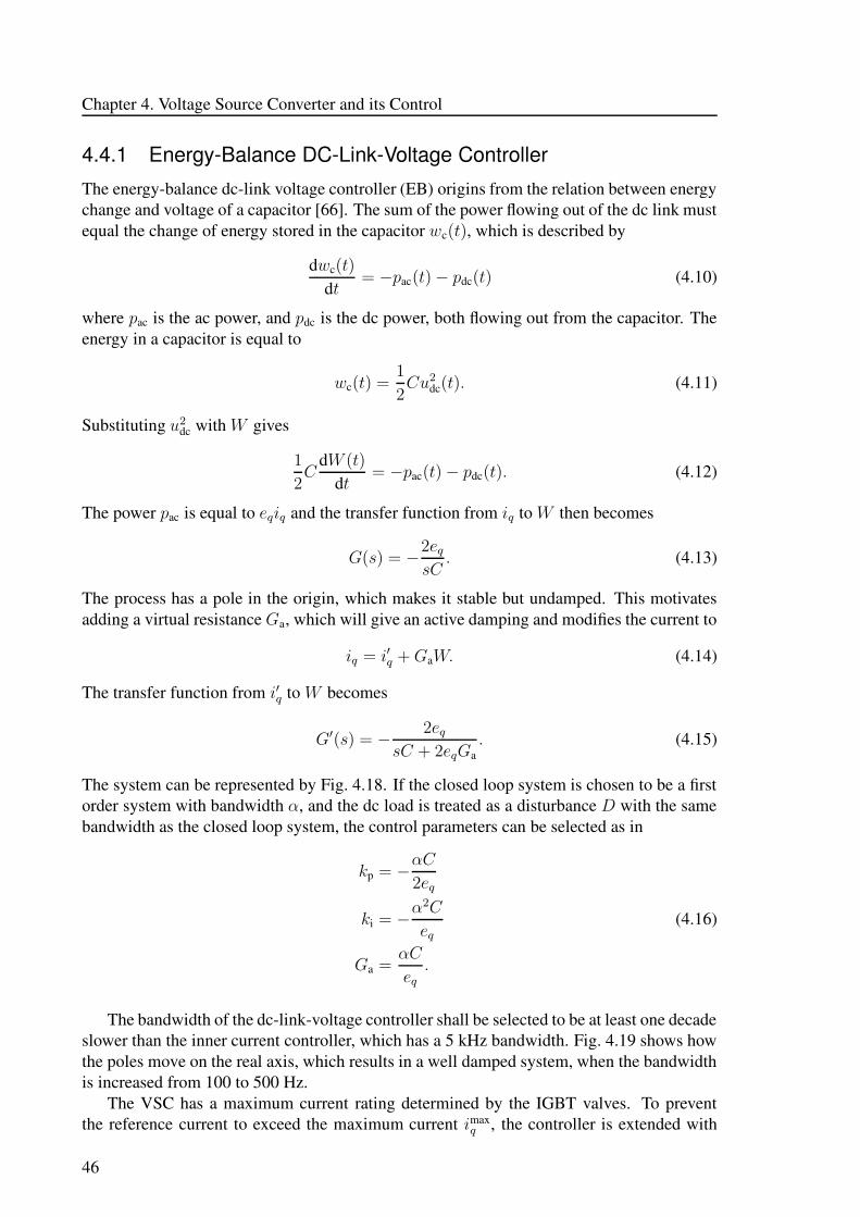
Chapter 4. Voltage Source Converter and its Control
4.4.1 Energy-Balance DC-Link-Voltage Controller
The energy-balance dc-link voltage controller (EB) origins from the relation between energychange and voltage of a capacitor [66]. The sum of the power flowing out of the dc link mustequal the change of energy stored in the capacitor wc(t), which is described by
dwc(t)
dt= −pac(t) − pdc(t) (4.10)
where pac is the ac power, and pdc is the dc power, both flowing out from the capacitor. Theenergy in a capacitor is equal to
wc(t) =1
2Cu2
dc(t). (4.11)
Substituting u2
dc with W gives
1
2C
dW (t)
dt= −pac(t) − pdc(t). (4.12)
The power pac is equal to eqiq and the transfer function from iq to W then becomes
G(s) = −2eq
sC. (4.13)
The process has a pole in the origin, which makes it stable but undamped. This motivatesadding a virtual resistance Ga, which will give an active damping and modifies the current to
iq = i′q + GaW. (4.14)
The transfer function from i′q to W becomes
G′(s) = −2eq
sC + 2eqGa. (4.15)
The system can be represented by Fig. 4.18. If the closed loop system is chosen to be a firstorder system with bandwidth α, and the dc load is treated as a disturbance D with the samebandwidth as the closed loop system, the control parameters can be selected as in
kp = −αC
2eq
ki = −α2C
eq
Ga =αC
eq
.
(4.16)
The bandwidth of the dc-link-voltage controller shall be selected to be at least one decadeslower than the inner current controller, which has a 5 kHz bandwidth. Fig. 4.19 shows howthe poles move on the real axis, which results in a well damped system, when the bandwidthis increased from 100 to 500 Hz.
The VSC has a maximum current rating determined by the IGBT valves. To preventthe reference current to exceed the maximum current imax
q , the controller is extended with
46
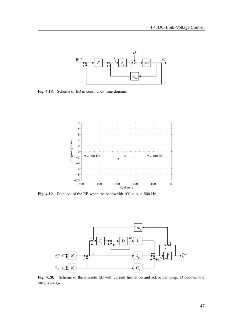
4.4. DC-Link-Voltage Control
F eq 1/sC
Ga
D
WrefW+ ++- -
-qi
Fig. 4.18. Scheme of EB in continuous time domain.
−500 −400 −300 −200 −100 0−10
−8
−6
−4
−2
0
2
4
6
8
10
Real axis
Imag
inar
y ax
is
α α = 100 Hz α = 500 Hz
Fig. 4.19. Pole loci of the EB when the bandwidth 100 < α < 500 Hz.
1/kp
D kiTs
Ga
kp+ -
++
+ +
+ ++
-+
refdcu
dcu
refqi
refqi
ie
e
Fig. 4.20. Scheme of the discrete EB with current limitation and active damping. D denotes onesample delay.
47
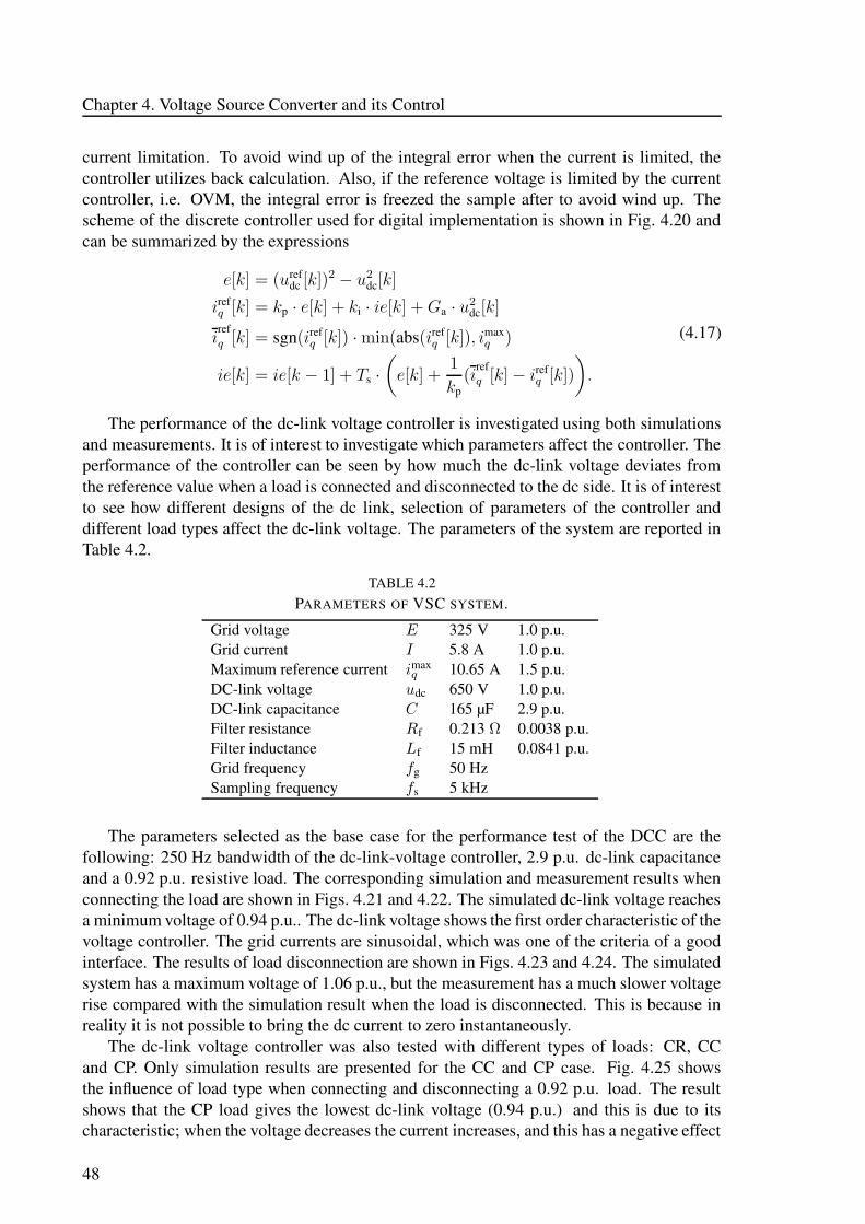
Chapter 4. Voltage Source Converter and its Control
current limitation. To avoid wind up of the integral error when the current is limited, thecontroller utilizes back calculation. Also, if the reference voltage is limited by the currentcontroller, i.e. OVM, the integral error is freezed the sample after to avoid wind up. Thescheme of the discrete controller used for digital implementation is shown in Fig. 4.20 andcan be summarized by the expressions
e[k] = (urefdc [k])2 − u2
dc[k]
irefq [k] = kp · e[k] + ki · ie[k] + Ga · u
2
dc[k]
irefq [k] = sgn(iref
q [k]) · min(abs(irefq [k]), imax
q )
ie[k] = ie[k − 1] + Ts ·
(
e[k] +1
kp(i
refq [k] − iref
q [k])
)
.
(4.17)
The performance of the dc-link voltage controller is investigated using both simulationsand measurements. It is of interest to investigate which parameters affect the controller. Theperformance of the controller can be seen by how much the dc-link voltage deviates fromthe reference value when a load is connected and disconnected to the dc side. It is of interestto see how different designs of the dc link, selection of parameters of the controller anddifferent load types affect the dc-link voltage. The parameters of the system are reported inTable 4.2.
TABLE 4.2PARAMETERS OF VSC SYSTEM.
Grid voltage E 325 V 1.0 p.u.Grid current I 5.8 A 1.0 p.u.Maximum reference current imax
q 10.65 A 1.5 p.u.DC-link voltage udc 650 V 1.0 p.u.DC-link capacitance C 165 µF 2.9 p.u.Filter resistance Rf 0.213 Ω 0.0038 p.u.Filter inductance Lf 15 mH 0.0841 p.u.Grid frequency fg 50 HzSampling frequency fs 5 kHz
The parameters selected as the base case for the performance test of the DCC are thefollowing: 250 Hz bandwidth of the dc-link-voltage controller, 2.9 p.u. dc-link capacitanceand a 0.92 p.u. resistive load. The corresponding simulation and measurement results whenconnecting the load are shown in Figs. 4.21 and 4.22. The simulated dc-link voltage reachesa minimum voltage of 0.94 p.u.. The dc-link voltage shows the first order characteristic of thevoltage controller. The grid currents are sinusoidal, which was one of the criteria of a goodinterface. The results of load disconnection are shown in Figs. 4.23 and 4.24. The simulatedsystem has a maximum voltage of 1.06 p.u., but the measurement has a much slower voltagerise compared with the simulation result when the load is disconnected. This is because inreality it is not possible to bring the dc current to zero instantaneously.
The dc-link voltage controller was also tested with different types of loads: CR, CCand CP. Only simulation results are presented for the CC and CP case. Fig. 4.25 showsthe influence of load type when connecting and disconnecting a 0.92 p.u. load. The resultshows that the CP load gives the lowest dc-link voltage (0.94 p.u.) and this is due to itscharacteristic; when the voltage decreases the current increases, and this has a negative effect
48
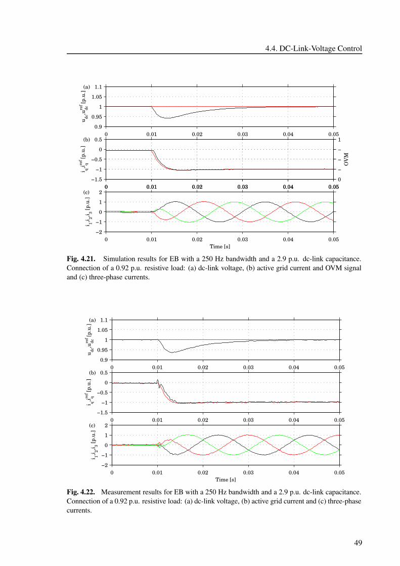
4.4. DC-Link-Voltage Control
0 0.01 0.02 0.03 0.04 0.050.9
0.95
1
1.05
1.1u dc
,udcre
f [p.u
.](a)
0 0.01 0.02 0.03 0.04 0.05−1.5
−1
−0.5
0
0.5
i q,i qref [p
.u.]
0 0.01 0.02 0.03 0.04 0.050
−
−
−
1
OV
M
(b)
0 0.01 0.02 0.03 0.04 0.05−2
−1
0
1
2
Time [s]
i 1,i 2,i 3 [p.u
.]
(c)
Fig. 4.21. Simulation results for EB with a 250 Hz bandwidth and a 2.9 p.u. dc-link capacitance.Connection of a 0.92 p.u. resistive load: (a) dc-link voltage, (b) active grid current and OVM signaland (c) three-phase currents.
0 0.01 0.02 0.03 0.04 0.050.9
0.95
1
1.05
1.1
u dc,u
dcref [p
.u.]
(a)
0 0.01 0.02 0.03 0.04 0.05−1.5
−1
−0.5
0
0.5
i q,i qref [p
.u.]
(b)
0 0.01 0.02 0.03 0.04 0.05−2
−1
0
1
2
i 1,i 2,i 3 [p.u
.]
(c)
Time [s]
Fig. 4.22. Measurement results for EB with a 250 Hz bandwidth and a 2.9 p.u. dc-link capacitance.Connection of a 0.92 p.u. resistive load: (a) dc-link voltage, (b) active grid current and (c) three-phasecurrents.
49
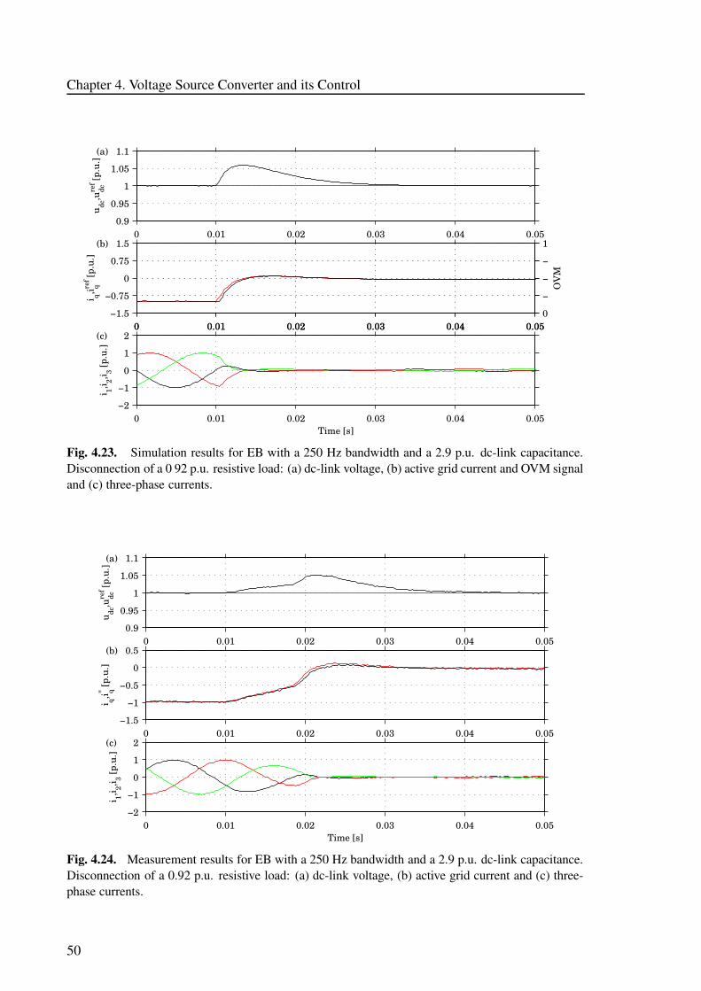
Chapter 4. Voltage Source Converter and its Control
0 0.01 0.02 0.03 0.04 0.050.9
0.95
1
1.05
1.1
u dc,u
dcref [p
.u.]
(a)
0 0.01 0.02 0.03 0.04 0.05−1.5
−0.75
0
0.75
1.5
i q,i qref [p
.u.]
0 0.01 0.02 0.03 0.04 0.050
−
−
−
1
OV
M
(b)
0 0.01 0.02 0.03 0.04 0.05−2
−1
0
1
2
Time [s]
i 1,i 2,i 3 [p.u
.]
(c)
Fig. 4.23. Simulation results for EB with a 250 Hz bandwidth and a 2.9 p.u. dc-link capacitance.Disconnection of a 0 92 p.u. resistive load: (a) dc-link voltage, (b) active grid current and OVM signaland (c) three-phase currents.
0 0.01 0.02 0.03 0.04 0.050.9
0.95
1
1.05
1.1
u dc,u
dcref [p
.u.]
(a)
0 0.01 0.02 0.03 0.04 0.05−1.5
−1
−0.5
0
0.5
i q,i q* [p.u
.]
(b)
0 0.01 0.02 0.03 0.04 0.05−2
−1
0
1
2
i 1,i 2,i 3 [p.u
.]
(c)
Time [s]
Fig. 4.24. Measurement results for EB with a 250 Hz bandwidth and a 2.9 p.u. dc-link capacitance.Disconnection of a 0.92 p.u. resistive load: (a) dc-link voltage, (b) active grid current and (c) three-phase currents.
50

4.4. DC-Link-Voltage Control
on the system. When disconnecting a load, the type does not affect the system since the loadis not connected.
0 0.01 0.02 0.03 0.04 0.050.9
0.95
1
1.05
1.1
u dc,u
dcref [p
.u.]
(a)
0 0.01 0.02 0.03 0.04 0.050.9
0.95
1
1.05
1.1(b)
u dc,u
dcref [p
.u.]
Time [s]
Fig. 4.25. Simulation result for EB with a 250 Hz bandwidth and a 2.9 p.u. dc-link capacitance.Connection (a) and disconnection (b) of different types of loads: CR (solid), CC (dashed) and CP(dashed dotted).
The size of the dc-link has a great impact on the performance of the system. A biggercapacitor does not require a fast voltage controller since the transient energy can be takenfrom it without the voltage being affected. However, a bigger capacitor will lead to a highercost. Fig. 4.26 shows the simulation result where different sizes of the dc-link capacitancehave been tested. Capacitances of 1.45, 2.9 and 5.8 p.u. have been used when connectingand disconnecting a 0.92 p.u. resistive load. The minimum value of the dc-link voltagewhen connecting the load was 0.89, 0.94 and 0.97 p.u. for 1.45, 2.9 and 5.8 p.u. dc-linkcapacitance, respectively, and the maximum value was 1.12, 1.06 and 1.03 p.u. for the samecapacitors. A bigger capacitor will reduce the deviation from the reference value.
0 0.01 0.02 0.03 0.04 0.050.85
0.9
0.95
1
1.05
u dc,u
dcref [p
.u.]
(a)
0 0.01 0.02 0.03 0.04 0.050.95
1
1.05
1.1
1.15(b)
u dc,u
dcref [p
.u.]
Time [s]
Fig. 4.26. Simulation result EB with a 250 Hz bandwidth. Connection (a) and disconnection (b)of a 0.92 p.u. resistive load, with 1.45 (dashed dotted), 2.9 (solid) and 5.8 p.u. (dashed) dc-linkcapacitance.
The bandwidth of the controller also determines the performance of the system. A fastercontroller can result in a smaller size of capacitance. Bandwidths of 250 and 500 Hz have
51
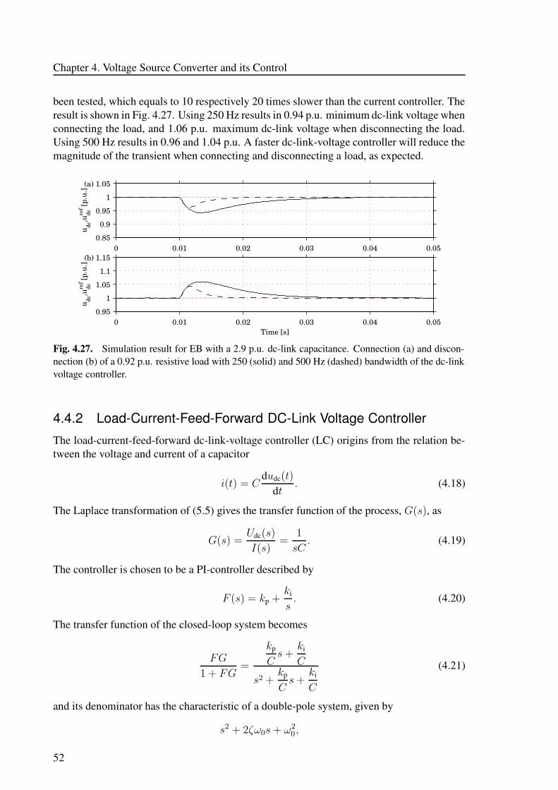
Chapter 4. Voltage Source Converter and its Control
been tested, which equals to 10 respectively 20 times slower than the current controller. Theresult is shown in Fig. 4.27. Using 250 Hz results in 0.94 p.u. minimum dc-link voltage whenconnecting the load, and 1.06 p.u. maximum dc-link voltage when disconnecting the load.Using 500 Hz results in 0.96 and 1.04 p.u. A faster dc-link-voltage controller will reduce themagnitude of the transient when connecting and disconnecting a load, as expected.
0 0.01 0.02 0.03 0.04 0.050.85
0.9
0.95
1
1.05
u dc,u
dcref [p
.u.]
(a)
0 0.01 0.02 0.03 0.04 0.050.95
1
1.05
1.1
1.15(b)
u dc,u
dcref [p
.u.]
Time [s]
Fig. 4.27. Simulation result for EB with a 2.9 p.u. dc-link capacitance. Connection (a) and discon-nection (b) of a 0.92 p.u. resistive load with 250 (solid) and 500 Hz (dashed) bandwidth of the dc-linkvoltage controller.
4.4.2 Load-Current-Feed-Forward DC-Link Voltage Controller
The load-current-feed-forward dc-link-voltage controller (LC) origins from the relation be-tween the voltage and current of a capacitor
i(t) = Cdudc(t)
dt. (4.18)
The Laplace transformation of (5.5) gives the transfer function of the process, G(s), as
G(s) =Udc(s)
I(s)=
1
sC. (4.19)
The controller is chosen to be a PI-controller described by
F (s) = kp +ki
s. (4.20)
The transfer function of the closed-loop system becomes
FG
1 + FG=
kp
Cs +
ki
C
s2 +kp
Cs +
ki
C
(4.21)
and its denominator has the characteristic of a double-pole system, given by
s2 + 2ζω0s + ω2
0,
52
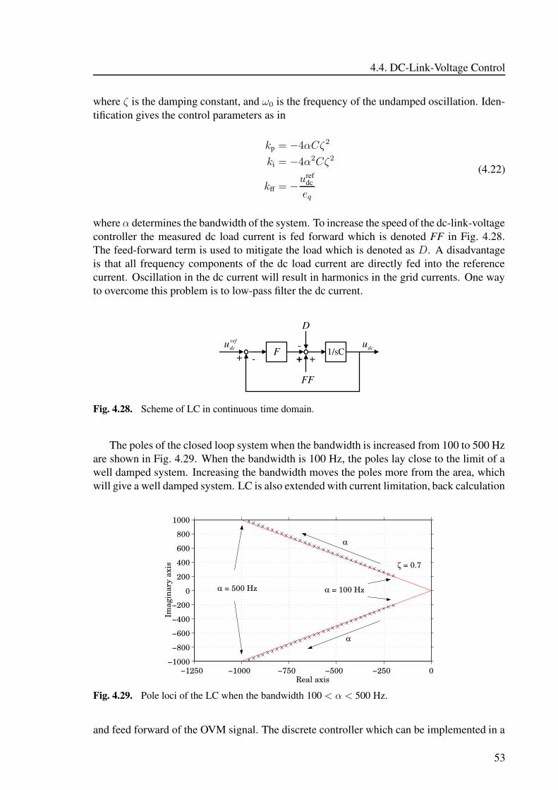
4.4. DC-Link-Voltage Control
where ζ is the damping constant, and ω0 is the frequency of the undamped oscillation. Iden-tification gives the control parameters as in
kp = −4αCζ2
ki = −4α2Cζ2
kff = −uref
dc
eq
(4.22)
where α determines the bandwidth of the system. To increase the speed of the dc-link-voltagecontroller the measured dc load current is fed forward which is denoted FF in Fig. 4.28.The feed-forward term is used to mitigate the load which is denoted as D. A disadvantageis that all frequency components of the dc load current are directly fed into the referencecurrent. Oscillation in the dc current will result in harmonics in the grid currents. One wayto overcome this problem is to low-pass filter the dc current.
F 1/sC
Drefdcu
+ ++-- dcu
+
FF
Fig. 4.28. Scheme of LC in continuous time domain.
The poles of the closed loop system when the bandwidth is increased from 100 to 500 Hzare shown in Fig. 4.29. When the bandwidth is 100 Hz, the poles lay close to the limit of awell damped system. Increasing the bandwidth moves the poles more from the area, whichwill give a well damped system. LC is also extended with current limitation, back calculation
−1250 −1000 −750 −500 −250 0−1000
−800
−600
−400
−200
0
200
400
600
800
1000
Real axis
Imag
inar
y ax
is
α = 500 Hz α = 100 Hz
ζ = 0.7
α
α
Fig. 4.29. Pole loci of the LC when the bandwidth 100 < α < 500 Hz.
and feed forward of the OVM signal. The discrete controller which can be implemented in a
53
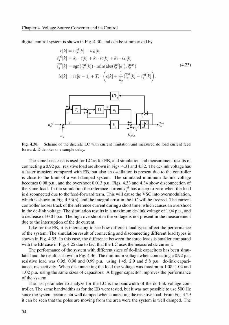
Chapter 4. Voltage Source Converter and its Control
digital control system is shown in Fig. 4.30, and can be summarized by
e[k] = urefdc [k] − udc[k]
irefq [k] = kp · e[k] + ki · ie[k] + kff · idc[k]
irefq [k] = sgn(iref
q [k]) · min(abs(irefq [k]), imax
q )
ie[k] = ie[k − 1] + Ts ·
(
e[k] +1
kp(i
refq [k] − iref
q [k]
)
.
(4.23)
1/kp
D kiTs
kp+ -
++
+ +
++
-+
refdcu
dcu
refqi
refqi
ie
e+
dcff ik
Fig. 4.30. Scheme of the discrete LC with current limitation and measured dc load current feedforward. D denotes one sample delay.
The same base case is used for LC as for EB, and simulation and measurement results ofconnecting a 0.92 p.u. resistive load are shown in Figs. 4.31 and 4.32. The dc-link voltage hasa faster transient compared with EB, but also an oscillation is present due to the controlleris close to the limit of a well-damped system. The simulated minimum dc-link voltagebecomes 0.98 p.u., and the overshoot 0.013 p.u. Figs. 4.33 and 4.34 show disconnection ofthe same load. In the simulation the reference current iref
q has a step to zero when the loadis disconnected due to the feed-forward term. This will cause the VSC into overmodulation,which is shown in Fig. 4.33(b), and the integral error in the LC will be freezed. The currentcontroller looses track of the reference current during a short time, which causes an overshootin the dc-link voltage. The simulation results in a maximum dc-link voltage of 1.04 p.u., anda decrease of 0.01 p.u. The high overshoot in the voltage is not present in the measurementdue to the interruption of the dc current.
Like for the EB, it is interesting to see how different load types affect the performanceof the system. The simulation result of connecting and disconnecting different load types isshown in Fig. 4.35. In this case, the difference between the three loads is smaller comparedwith the EB case in Fig. 4.25 due to fact that the LC uses the measured dc current.
The performance of the system with different sizes of dc-link capacitors has been simu-lated and the result is shown in Fig. 4.36. The minimum voltage when connecting a 0.92 p.u.resistive load was 0.95, 0.98 and 0.99 p.u. using 1.45, 2.9 and 5.8 p.u. dc-link capaci-tance, respectively. When disconnecting the load the voltage was maximum 1.08, 1.04 and1.02 p.u. using the same sizes of capacitors. A bigger capacitor improves the performanceof the system.
The last parameter to analyze for the LC is the bandwidth of the dc-link voltage con-troller. The same bandwidths as for the EB were tested, but it was not possible to use 500 Hzsince the system became not well damped when connecting the resistive load. From Fig. 4.29it can be seen that the poles are moving from the area were the system is well damped. The
54
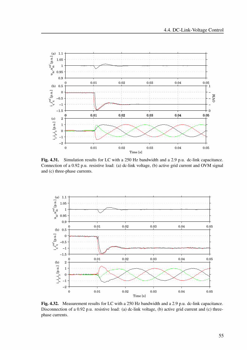
4.4. DC-Link-Voltage Control
0 0.01 0.02 0.03 0.04 0.050.9
0.95
1
1.05
1.1u dc
,udcre
f [p.u
.](a)
0 0.01 0.02 0.03 0.04 0.05−1.5
−1
−0.5
0
0.5
i q,i qref [p
.u.]
0 0.01 0.02 0.03 0.04 0.050
−
−
−
1
OV
M
(b)
0 0.01 0.02 0.03 0.04 0.05−2
−1
0
1
2
Time [s]
i 1,i 2,i 3 [p.u
.]
(c)
Fig. 4.31. Simulation results for LC with a 250 Hz bandwidth and a 2.9 p.u. dc-link capacitance.Connection of a 0.92 p.u. resistive load: (a) dc-link voltage, (b) active grid current and OVM signaland (c) three-phase currents.
0 0.01 0.02 0.03 0.04 0.050.9
0.95
1
1.05
1.1
u dc,u
dcref [p
.u.]
(a)
0 0.01 0.02 0.03 0.04 0.05−1.5
−1
−0.5
0
0.5
i q,i qref [p
.u.]
(b)
0 0.01 0.02 0.03 0.04 0.05−2
−1
0
1
2
i 1,i 2,i 3 [p.u
.]
(b)
Time [s]
Fig. 4.32. Measurement results for LC with a 250 Hz bandwidth and a 2.9 p.u. dc-link capacitance.Disconnection of a 0.92 p.u. resistive load: (a) dc-link voltage, (b) active grid current and (c) three-phase currents.
55
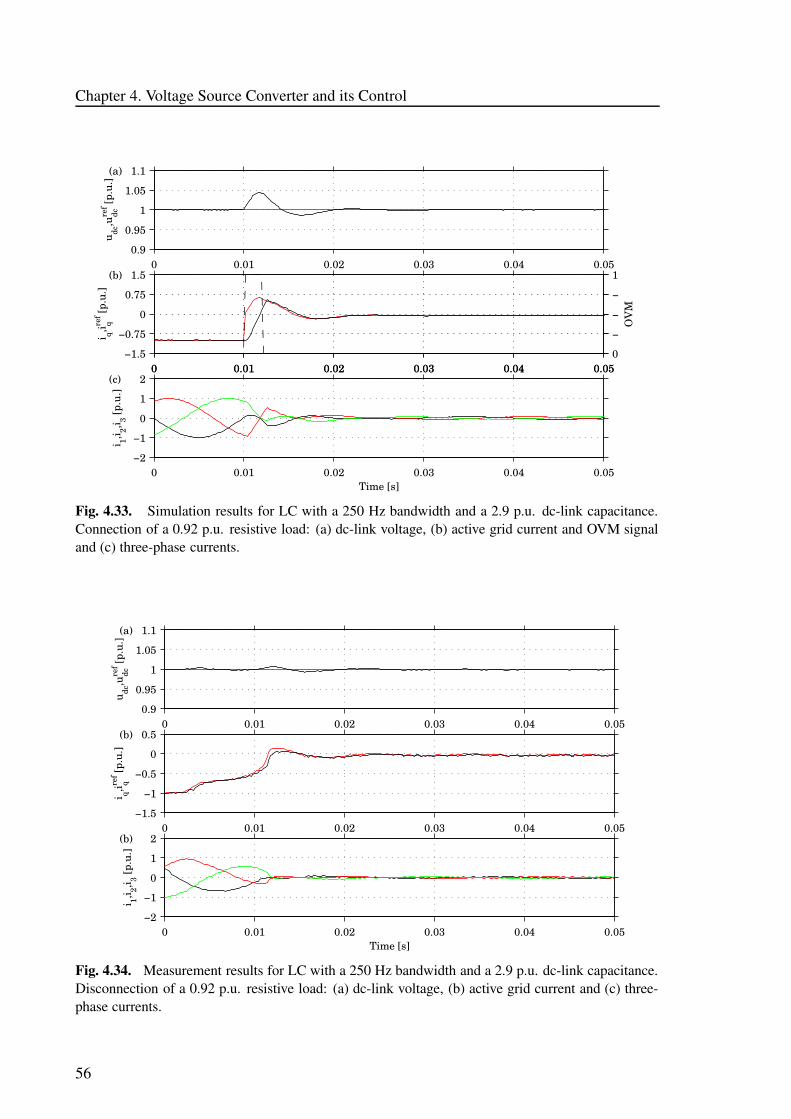
Chapter 4. Voltage Source Converter and its Control
0 0.01 0.02 0.03 0.04 0.050.9
0.95
1
1.05
1.1
u dc,u
dcref [p
.u.]
(a)
0 0.01 0.02 0.03 0.04 0.05−1.5
−0.75
0
0.75
1.5
i q,i qref [p
.u.]
0 0.01 0.02 0.03 0.04 0.050
−
−
−
1
OV
M
(b)
0 0.01 0.02 0.03 0.04 0.05−2
−1
0
1
2
Time [s]
i 1,i 2,i 3 [p.u
.]
(c)
Fig. 4.33. Simulation results for LC with a 250 Hz bandwidth and a 2.9 p.u. dc-link capacitance.Connection of a 0.92 p.u. resistive load: (a) dc-link voltage, (b) active grid current and OVM signaland (c) three-phase currents.
0 0.01 0.02 0.03 0.04 0.050.9
0.95
1
1.05
1.1
u dc,u
dcref [p
.u.]
(a)
0 0.01 0.02 0.03 0.04 0.05−1.5
−1
−0.5
0
0.5
i q,i qref [p
.u.]
(b)
0 0.01 0.02 0.03 0.04 0.05−2
−1
0
1
2
i 1,i 2,i 3 [p.u
.]
(b)
Time [s]
Fig. 4.34. Measurement results for LC with a 250 Hz bandwidth and a 2.9 p.u. dc-link capacitance.Disconnection of a 0.92 p.u. resistive load: (a) dc-link voltage, (b) active grid current and (c) three-phase currents.
56
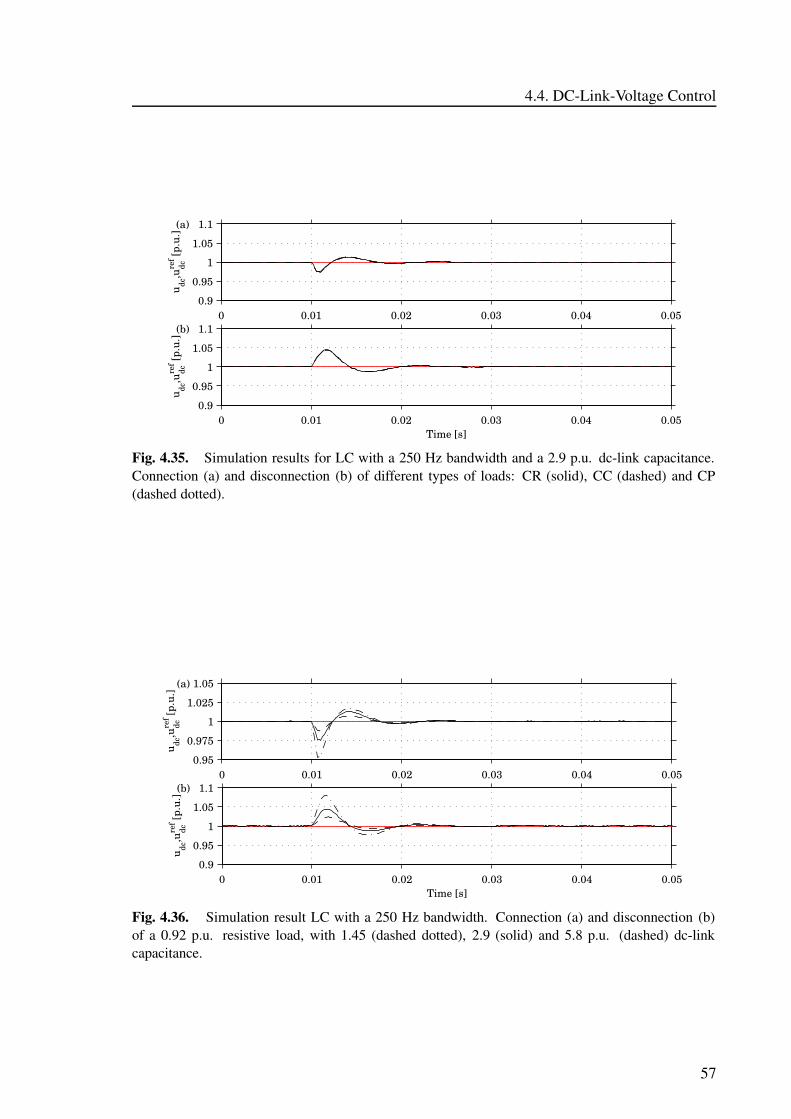
4.4. DC-Link-Voltage Control
0 0.01 0.02 0.03 0.04 0.050.9
0.95
1
1.05
1.1
u dc,u
dcref [p
.u.]
(a)
0 0.01 0.02 0.03 0.04 0.050.9
0.95
1
1.05
1.1(b)
u dc,u
dcref [p
.u.]
Time [s]
Fig. 4.35. Simulation results for LC with a 250 Hz bandwidth and a 2.9 p.u. dc-link capacitance.Connection (a) and disconnection (b) of different types of loads: CR (solid), CC (dashed) and CP(dashed dotted).
0 0.01 0.02 0.03 0.04 0.050.95
0.975
1
1.025
1.05
u dc,u
dcref [p
.u.]
(a)
0 0.01 0.02 0.03 0.04 0.050.9
0.95
1
1.05
1.1(b)
u dc,u
dcref [p
.u.]
Time [s]
Fig. 4.36. Simulation result LC with a 250 Hz bandwidth. Connection (a) and disconnection (b)of a 0.92 p.u. resistive load, with 1.45 (dashed dotted), 2.9 (solid) and 5.8 p.u. (dashed) dc-linkcapacitance.
57
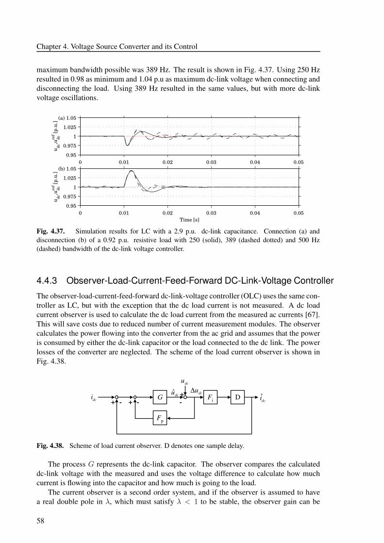
Chapter 4. Voltage Source Converter and its Control
maximum bandwidth possible was 389 Hz. The result is shown in Fig. 4.37. Using 250 Hzresulted in 0.98 as minimum and 1.04 p.u as maximum dc-link voltage when connecting anddisconnecting the load. Using 389 Hz resulted in the same values, but with more dc-linkvoltage oscillations.
0 0.01 0.02 0.03 0.04 0.050.95
0.975
1
1.025
1.05
u dc,u
dcref [p
.u.]
(a)
0 0.01 0.02 0.03 0.04 0.050.95
0.975
1
1.025
1.05(b)
u dc,u
dcref [p
.u.]
Time [s]
Fig. 4.37. Simulation results for LC with a 2.9 p.u. dc-link capacitance. Connection (a) anddisconnection (b) of a 0.92 p.u. resistive load with 250 (solid), 389 (dashed dotted) and 500 Hz(dashed) bandwidth of the dc-link voltage controller.
4.4.3 Observer-Load-Current-Feed-Forward DC-Link-Voltage Controller
The observer-load-current-feed-forward dc-link-voltage controller (OLC) uses the same con-troller as LC, but with the exception that the dc load current is not measured. A dc loadcurrent observer is used to calculate the dc load current from the measured ac currents [67].This will save costs due to reduced number of current measurement modules. The observercalculates the power flowing into the converter from the ac grid and assumes that the poweris consumed by either the dc-link capacitor or the load connected to the dc link. The powerlosses of the converter are neglected. The scheme of the load current observer is shown inFig. 4.38.
G-+
-+
Fp
DFi-+dci
dcu
dcudci
dcu∆
Fig. 4.38. Scheme of load current observer. D denotes one sample delay.
The process G represents the dc-link capacitor. The observer compares the calculateddc-link voltage with the measured and uses the voltage difference to calculate how muchcurrent is flowing into the capacitor and how much is going to the load.
The current observer is a second order system, and if the observer is assumed to havea real double pole in λ, which must satisfy λ < 1 to be stable, the observer gain can be
58
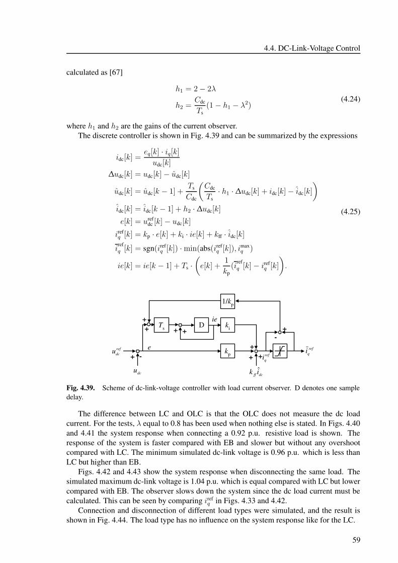
4.4. DC-Link-Voltage Control
calculated as [67]
h1 = 2 − 2λ
h2 =Cdc
Ts(1 − h1 − λ2)
(4.24)
where h1 and h2 are the gains of the current observer.The discrete controller is shown in Fig. 4.39 and can be summarized by the expressions
idc[k] =eq[k] · iq[k]
udc[k]
∆udc[k] = udc[k] − udc[k]
udc[k] = udc[k − 1] +Ts
Cdc
(
Cdc
Ts· h1 · ∆udc[k] + idc[k] − idc[k]
)
idc[k] = idc[k − 1] + h2 · ∆udc[k]
e[k] = urefdc [k] − udc[k]
irefq [k] = kp · e[k] + ki · ie[k] + kff · idc[k]
irefq [k] = sgn(iref
q [k]) · min(abs(irefq [k]), imax
q )
ie[k] = ie[k − 1] + Ts ·
(
e[k] +1
kp(i
refq [k] − iref
q [k]
)
.
(4.25)
1/kp
D kiTs
kp+ -
++
+ +
++
-+
refdcu
dcu
refqi
refqi
ie
e+
dcff ik ˆ
Fig. 4.39. Scheme of dc-link-voltage controller with load current observer. D denotes one sampledelay.
The difference between LC and OLC is that the OLC does not measure the dc loadcurrent. For the tests, λ equal to 0.8 has been used when nothing else is stated. In Figs. 4.40and 4.41 the system response when connecting a 0.92 p.u. resistive load is shown. Theresponse of the system is faster compared with EB and slower but without any overshootcompared with LC. The minimum simulated dc-link voltage is 0.96 p.u. which is less thanLC but higher than EB.
Figs. 4.42 and 4.43 show the system response when disconnecting the same load. Thesimulated maximum dc-link voltage is 1.04 p.u. which is equal compared with LC but lowercompared with EB. The observer slows down the system since the dc load current must becalculated. This can be seen by comparing iref
q in Figs. 4.33 and 4.42.Connection and disconnection of different load types were simulated, and the result is
shown in Fig. 4.44. The load type has no influence on the system response like for the LC.
59
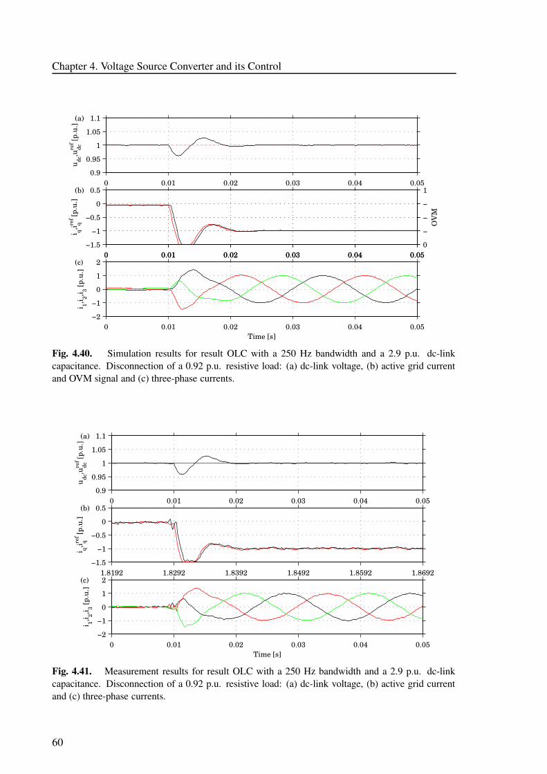
Chapter 4. Voltage Source Converter and its Control
0 0.01 0.02 0.03 0.04 0.050.9
0.95
1
1.05
1.1
u dc,u
dcref [p
.u.]
(a)
0 0.01 0.02 0.03 0.04 0.05−1.5
−1
−0.5
0
0.5
i q,i qref [p
.u.]
0 0.01 0.02 0.03 0.04 0.050
−
−
−
1
OV
M
(b)
0 0.01 0.02 0.03 0.04 0.05−2
−1
0
1
2
Time [s]
i 1,i 2,i 3 [p.u
.]
(c)
Fig. 4.40. Simulation results for result OLC with a 250 Hz bandwidth and a 2.9 p.u. dc-linkcapacitance. Disconnection of a 0.92 p.u. resistive load: (a) dc-link voltage, (b) active grid currentand OVM signal and (c) three-phase currents.
0 0.01 0.02 0.03 0.04 0.050.9
0.95
1
1.05
1.1
u dc,u
dcref [p
.u.]
(a)
1.8192 1.8292 1.8392 1.8492 1.8592 1.8692−1.5
−1
−0.5
0
0.5
i q,i qref [p
.u.]
(b)
0 0.01 0.02 0.03 0.04 0.05−2
−1
0
1
2
i 1,i 2,i 3 [p.u
.]
(c)
Time [s]
Fig. 4.41. Measurement results for result OLC with a 250 Hz bandwidth and a 2.9 p.u. dc-linkcapacitance. Disconnection of a 0.92 p.u. resistive load: (a) dc-link voltage, (b) active grid currentand (c) three-phase currents.
60
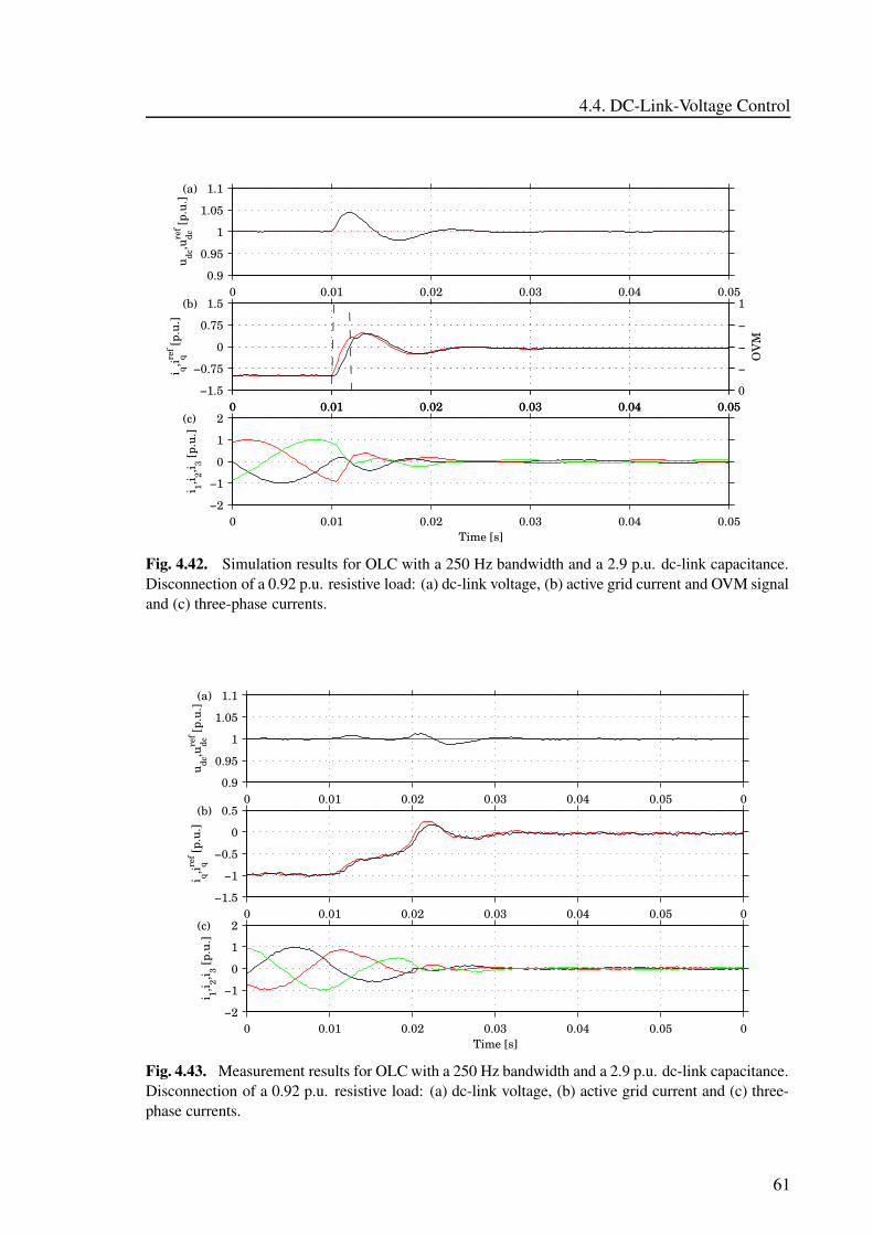
4.4. DC-Link-Voltage Control
0 0.01 0.02 0.03 0.04 0.050.9
0.95
1
1.05
1.1u dc
,udcre
f [p.u
.](a)
0 0.01 0.02 0.03 0.04 0.05−1.5
−0.75
0
0.75
1.5
i q,i qref [p
.u.]
0 0.01 0.02 0.03 0.04 0.050
−
−
−
1
OV
M
(b)
0 0.01 0.02 0.03 0.04 0.05−2
−1
0
1
2
Time [s]
i 1,i 2,i 3 [p.u
.]
(c)
Fig. 4.42. Simulation results for OLC with a 250 Hz bandwidth and a 2.9 p.u. dc-link capacitance.Disconnection of a 0.92 p.u. resistive load: (a) dc-link voltage, (b) active grid current and OVM signaland (c) three-phase currents.
0 0.01 0.02 0.03 0.04 0.05 00.9
0.95
1
1.05
1.1
u dc,u
dcref [p
.u.]
(a)
0 0.01 0.02 0.03 0.04 0.05 0−1.5
−1
−0.5
0
0.5
i q,i qref [p
.u.]
(b)
0 0.01 0.02 0.03 0.04 0.05 0−2
−1
0
1
2
i 1,i 2,i 3 [p.u
.]
(c)
Time [s]
Fig. 4.43. Measurement results for OLC with a 250 Hz bandwidth and a 2.9 p.u. dc-link capacitance.Disconnection of a 0.92 p.u. resistive load: (a) dc-link voltage, (b) active grid current and (c) three-phase currents.
61
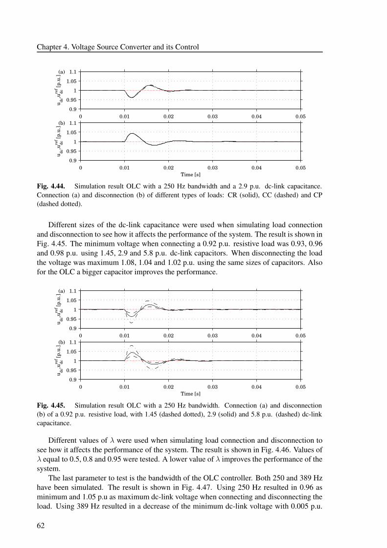
Chapter 4. Voltage Source Converter and its Control
0 0.01 0.02 0.03 0.04 0.050.9
0.95
1
1.05
1.1
u dc,u
dcref [p
.u.]
(a)
0 0.01 0.02 0.03 0.04 0.050.9
0.95
1
1.05
1.1(b)
u dc,u
dcref [p
.u.]
Time [s]
Fig. 4.44. Simulation result OLC with a 250 Hz bandwidth and a 2.9 p.u. dc-link capacitance.Connection (a) and disconnection (b) of different types of loads: CR (solid), CC (dashed) and CP(dashed dotted).
Different sizes of the dc-link capacitance were used when simulating load connectionand disconnection to see how it affects the performance of the system. The result is shown inFig. 4.45. The minimum voltage when connecting a 0.92 p.u. resistive load was 0.93, 0.96and 0.98 p.u. using 1.45, 2.9 and 5.8 p.u. dc-link capacitors. When disconnecting the loadthe voltage was maximum 1.08, 1.04 and 1.02 p.u. using the same sizes of capacitors. Alsofor the OLC a bigger capacitor improves the performance.
0 0.01 0.02 0.03 0.04 0.050.9
0.95
1
1.05
1.1
u dc,u
dcref [p
.u.]
(a)
0 0.01 0.02 0.03 0.04 0.050.9
0.95
1
1.05
1.1(b)
u dc,u
dcref [p
.u.]
Time [s]
Fig. 4.45. Simulation result OLC with a 250 Hz bandwidth. Connection (a) and disconnection(b) of a 0.92 p.u. resistive load, with 1.45 (dashed dotted), 2.9 (solid) and 5.8 p.u. (dashed) dc-linkcapacitance.
Different values of λ were used when simulating load connection and disconnection tosee how it affects the performance of the system. The result is shown in Fig. 4.46. Values ofλ equal to 0.5, 0.8 and 0.95 were tested. A lower value of λ improves the performance of thesystem.
The last parameter to test is the bandwidth of the OLC controller. Both 250 and 389 Hzhave been simulated. The result is shown in Fig. 4.47. Using 250 Hz resulted in 0.96 asminimum and 1.05 p.u as maximum dc-link voltage when connecting and disconnecting theload. Using 389 Hz resulted in a decrease of the minimum dc-link voltage with 0.005 p.u.
62
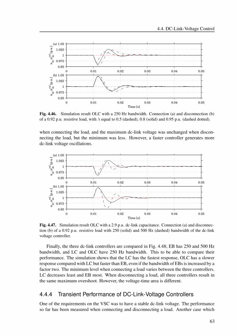
4.4. DC-Link-Voltage Control
0 0.01 0.02 0.03 0.04 0.050.95
0.975
1
1.025
1.05
u dc,u
dcref [p
.u.]
(a)
0 0.01 0.02 0.03 0.04 0.050.95
0.975
1
1.025
1.05(b)
u dc,u
dcref [p
.u.]
Time [s]
Fig. 4.46. Simulation result OLC with a 250 Hz bandwidth. Connection (a) and disconnection (b)of a 0.92 p.u. resistive load, with λ equal to 0.5 (dashed), 0.8 (solid) and 0.95 p.u. (dashed dotted).
when connecting the load, and the maximum dc-link voltage was unchanged when discon-necting the load, but the minimum was less. However, a faster controller generates moredc-link voltage oscillations.
0 0.01 0.02 0.03 0.04 0.050.95
0.975
1
1.025
1.05
u dc,u
dcref [p
.u.]
(a)
0 0.01 0.02 0.03 0.04 0.050.95
0.975
1
1.025
1.05(b)
u dc,u
dcref [p
.u.]
Time [s]
Fig. 4.47. Simulation result OLC with a 2.9 p.u. dc-link capacitance. Connection (a) and disconnec-tion (b) of a 0.92 p.u. resistive load with 250 (solid) and 500 Hz (dashed) bandwidth of the dc-linkvoltage controller.
Finally, the three dc-link controllers are compared in Fig. 4.48; EB has 250 and 500 Hzbandwidth, and LC and OLC have 250 Hz bandwidth. This to be able to compare theirperformance. The simulation shows that the LC has the fastest response, OLC has a slowerresponse compared with LC but faster than EB, even if the bandwidth of EBs is increased by afactor two. The minimum level when connecting a load varies between the three controllers.LC decreases least and EB most. When disconnecting a load, all three controllers result inthe same maximum overshoot. However, the voltage-time area is different.
4.4.4 Transient Performance of DC-Link-Voltage Controllers
One of the requirements on the VSC was to have a stable dc-link voltage. The performanceso far has been measured when connecting and disconnecting a load. Another case which
63
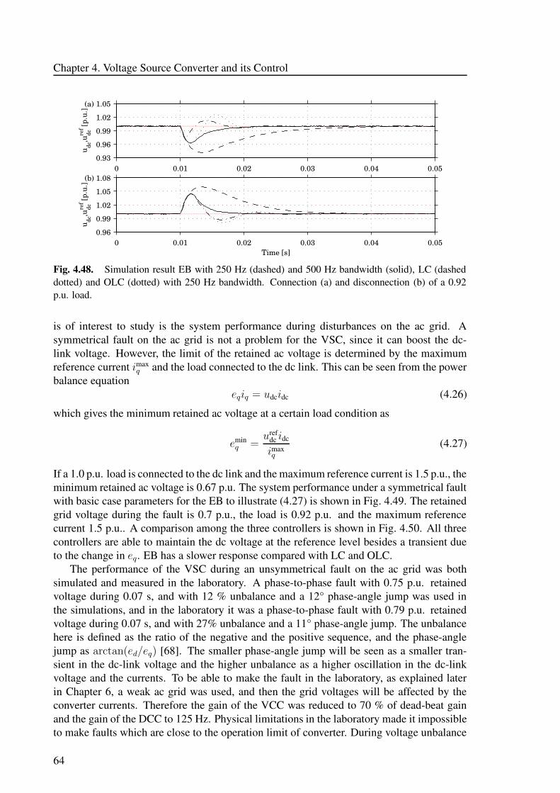
Chapter 4. Voltage Source Converter and its Control
0 0.01 0.02 0.03 0.04 0.050.93
0.96
0.99
1.02
1.05
u dc,u
dcref [p
.u.]
(a)
0 0.01 0.02 0.03 0.04 0.050.96
0.99
1.02
1.05
1.08(b)
u dc,u
dcref [p
.u.]
Time [s]
Fig. 4.48. Simulation result EB with 250 Hz (dashed) and 500 Hz bandwidth (solid), LC (dasheddotted) and OLC (dotted) with 250 Hz bandwidth. Connection (a) and disconnection (b) of a 0.92p.u. load.
is of interest to study is the system performance during disturbances on the ac grid. Asymmetrical fault on the ac grid is not a problem for the VSC, since it can boost the dc-link voltage. However, the limit of the retained ac voltage is determined by the maximumreference current imax
q and the load connected to the dc link. This can be seen from the powerbalance equation
eqiq = udcidc (4.26)
which gives the minimum retained ac voltage at a certain load condition as
eminq =
urefdc idc
imaxq
(4.27)
If a 1.0 p.u. load is connected to the dc link and the maximum reference current is 1.5 p.u., theminimum retained ac voltage is 0.67 p.u. The system performance under a symmetrical faultwith basic case parameters for the EB to illustrate (4.27) is shown in Fig. 4.49. The retainedgrid voltage during the fault is 0.7 p.u., the load is 0.92 p.u. and the maximum referencecurrent 1.5 p.u.. A comparison among the three controllers is shown in Fig. 4.50. All threecontrollers are able to maintain the dc voltage at the reference level besides a transient dueto the change in eq. EB has a slower response compared with LC and OLC.
The performance of the VSC during an unsymmetrical fault on the ac grid was bothsimulated and measured in the laboratory. A phase-to-phase fault with 0.75 p.u. retainedvoltage during 0.07 s, and with 12 % unbalance and a 12° phase-angle jump was used inthe simulations, and in the laboratory it was a phase-to-phase fault with 0.79 p.u. retainedvoltage during 0.07 s, and with 27% unbalance and a 11° phase-angle jump. The unbalancehere is defined as the ratio of the negative and the positive sequence, and the phase-anglejump as arctan(ed/eq) [68]. The smaller phase-angle jump will be seen as a smaller tran-sient in the dc-link voltage and the higher unbalance as a higher oscillation in the dc-linkvoltage and the currents. To be able to make the fault in the laboratory, as explained laterin Chapter 6, a weak ac grid was used, and then the grid voltages will be affected by theconverter currents. Therefore the gain of the VCC was reduced to 70 % of dead-beat gainand the gain of the DCC to 125 Hz. Physical limitations in the laboratory made it impossibleto make faults which are close to the operation limit of converter. During voltage unbalance
64
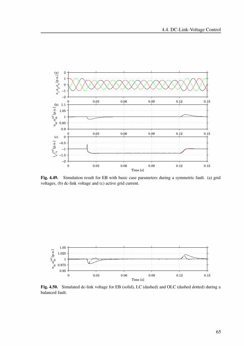
4.4. DC-Link-Voltage Control
0 0.03 0.06 0.09 0.12 0.15−2
−1
0
1
2
Time [s]
e 1,e2,e
3 [p.u
.]
(a)
0 0.03 0.06 0.09 0.12 0.150.9
0.95
1
1.05
1.1
u dc,u
dcref [p
.u.]
(b)
0 0.03 0.06 0.09 0.12 0.15−2
−1.5
−1
−0.5
0
i q,i qref [p
.u.]
(c)
Time [s]
Fig. 4.49. Simulation result for EB with basic case parameters during a symmetric fault. (a) gridvoltages, (b) dc-link voltage and (c) active grid current.
0 0.03 0.06 0.09 0.12 0.150.95
0.975
1
1.025
1.05
u dc,u
dcref [p
.u.]
Time [s]
Fig. 4.50. Simulated dc-link voltage for EB (solid), LC (dashed) and OLC (dashed dotted) during abalanced fault.
65
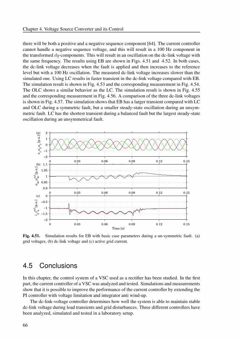
Chapter 4. Voltage Source Converter and its Control
there will be both a positive and a negative sequence component [64]. The current controllercannot handle a negative sequence voltage, and this will result in a 100 Hz component inthe transformed dq-components. This will result in an oscillation on the dc-link voltage withthe same frequency. The results using EB are shown in Figs. 4.51 and 4.52. In both cases,the dc-link voltage decreases when the fault is applied and then increases to the referencelevel but with a 100 Hz oscillation. The measured dc-link voltage increases slower than thesimulated one. Using LC results in faster transient in the dc-link voltage compared with EB.The simulation result is shown in Fig. 4.53 and the corresponding measurement in Fig. 4.54.The OLC shows a similar behavior as the LC. The simulation result is shown in Fig. 4.55and the corresponding measurement in Fig. 4.56. A comparison of the three dc-link voltagesis shown in Fig. 4.57. The simulation shows that EB has a larger transient compared with LCand OLC during a symmetric fault, but a smaller steady-state oscillation during an unsym-metric fault. LC has the shortest transient during a balanced fault but the largest steady-stateoscillation during an unsymmetrical fault.
0 0.03 0.06 0.09 0.12 0.15−2
−1
0
1
2
Time [s]
e 1,e2,e
3 [p.u
.]
(a)
0 0.03 0.06 0.09 0.12 0.150.9
0.95
1
1.05
1.1
u dc,u
dcref [p
.u.]
(b)
0 0.03 0.06 0.09 0.12 0.15−2
−1.5
−1
−0.5
0
i q,i qref [p
.u.]
(c)
Time [s]
Fig. 4.51. Simulation results for EB with basic case parameters during a un-symmetric fault. (a)grid voltages, (b) dc-link voltage and (c) active grid current.
4.5 Conclusions
In this chapter, the control system of a VSC used as a rectifier has been studied. In the firstpart, the current controller of a VSC was analyzed and tested. Simulations and measurementsshow that it is possible to improve the performance of the current controller by extending thePI controller with voltage limitation and integrator anti wind-up.
The dc-link-voltage controller determines how well the system is able to maintain stabledc-link voltage during load transients and grid disturbances. Three different controllers havebeen analyzed, simulated and tested in a laboratory setup.
66
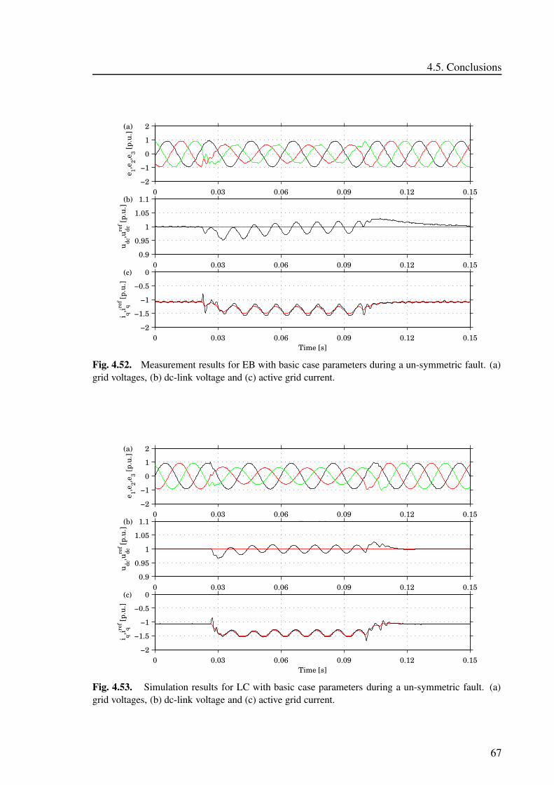
4.5. Conclusions
0 0.03 0.06 0.09 0.12 0.15−2
−1
0
1
2e 1,e
2,e3 [p
.u.]
(a)
0 0.03 0.06 0.09 0.12 0.150.9
0.95
1
1.05
1.1
u dc,u
dcref [p
.u.]
(b)
0 0.03 0.06 0.09 0.12 0.15−2
−1.5
−1
−0.5
0
i q,i qref [p
.u.]
(c)
Time [s]
Fig. 4.52. Measurement results for EB with basic case parameters during a un-symmetric fault. (a)grid voltages, (b) dc-link voltage and (c) active grid current.
0 0.03 0.06 0.09 0.12 0.15−2
−1
0
1
2
Time [s]
e 1,e2,e
3 [p.u
.]
(a)
0 0.03 0.06 0.09 0.12 0.150.9
0.95
1
1.05
1.1
u dc,u
dcref [p
.u.]
(b)
0 0.03 0.06 0.09 0.12 0.15−2
−1.5
−1
−0.5
0
i q,i qref [p
.u.]
(c)
Time [s]
Fig. 4.53. Simulation results for LC with basic case parameters during a un-symmetric fault. (a)grid voltages, (b) dc-link voltage and (c) active grid current.
67
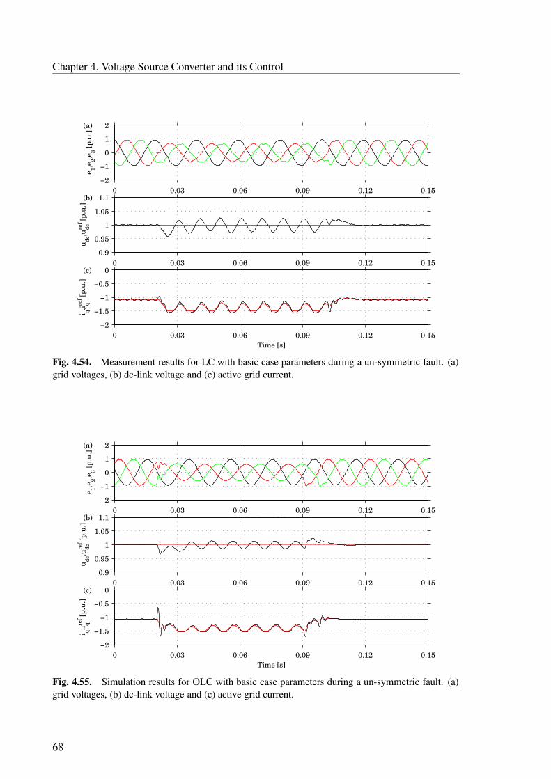
Chapter 4. Voltage Source Converter and its Control
0 0.03 0.06 0.09 0.12 0.15−2
−1
0
1
2
e 1,e2,e
3 [p.u
.]
(a)
0 0.03 0.06 0.09 0.12 0.150.9
0.95
1
1.05
1.1
u dc,u
dcref [p
.u.]
(b)
0 0.03 0.06 0.09 0.12 0.15−2
−1.5
−1
−0.5
0
i q,i qref [p
.u.]
(c)
Time [s]
Fig. 4.54. Measurement results for LC with basic case parameters during a un-symmetric fault. (a)grid voltages, (b) dc-link voltage and (c) active grid current.
0 0.03 0.06 0.09 0.12 0.15−2
−1
0
1
2
Time [s]
e 1,e2,e
3 [p.u
.]
(a)
0 0.03 0.06 0.09 0.12 0.150.9
0.95
1
1.05
1.1
u dc,u
dcref [p
.u.]
(b)
0 0.03 0.06 0.09 0.12 0.15−2
−1.5
−1
−0.5
0
i q,i qref [p
.u.]
(c)
Time [s]
Fig. 4.55. Simulation results for OLC with basic case parameters during a un-symmetric fault. (a)grid voltages, (b) dc-link voltage and (c) active grid current.
68
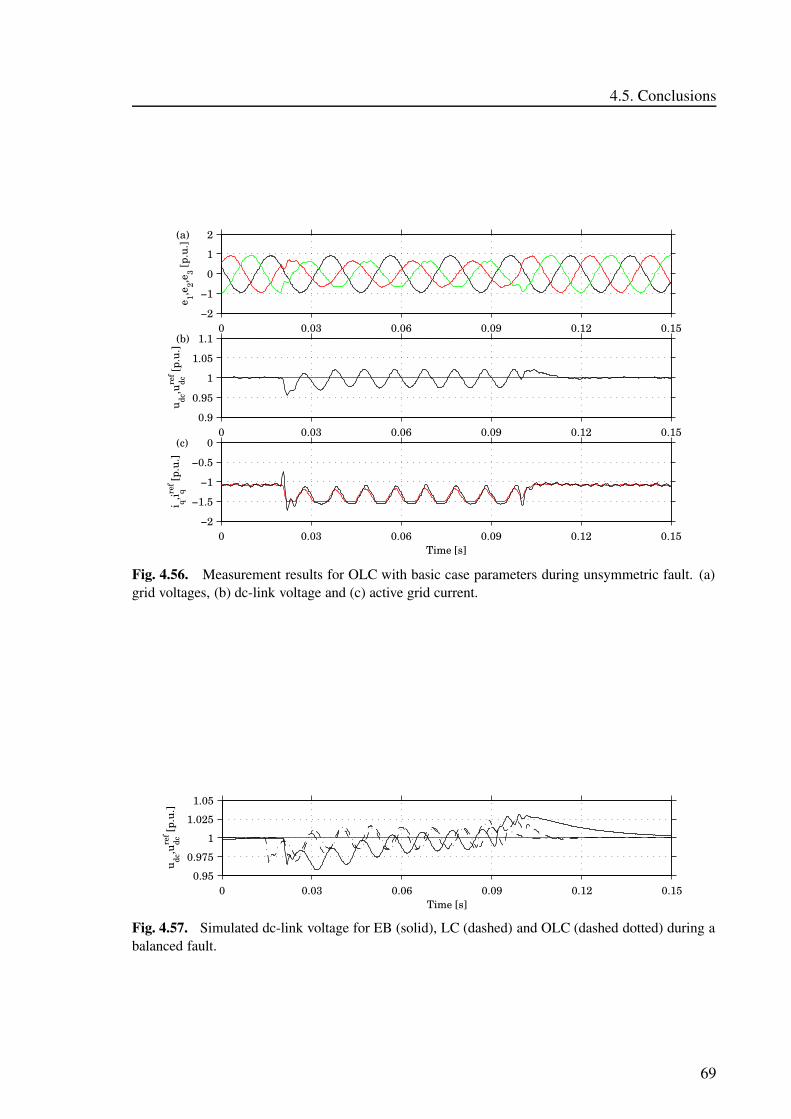
4.5. Conclusions
0 0.03 0.06 0.09 0.12 0.15−2
−1
0
1
2
e 1,e2,e
3 [p.u
.]
(a)
0 0.03 0.06 0.09 0.12 0.150.9
0.95
1
1.05
1.1
u dc,u
dcref [p
.u.]
(b)
0 0.03 0.06 0.09 0.12 0.15−2
−1.5
−1
−0.5
0
i q,i qref [p
.u.]
(c)
Time [s]
Fig. 4.56. Measurement results for OLC with basic case parameters during unsymmetric fault. (a)grid voltages, (b) dc-link voltage and (c) active grid current.
0 0.03 0.06 0.09 0.12 0.150.95
0.975
1
1.025
1.05
u dc,u
dcref [p
.u.]
Time [s]
Fig. 4.57. Simulated dc-link voltage for EB (solid), LC (dashed) and OLC (dashed dotted) during abalanced fault.
69
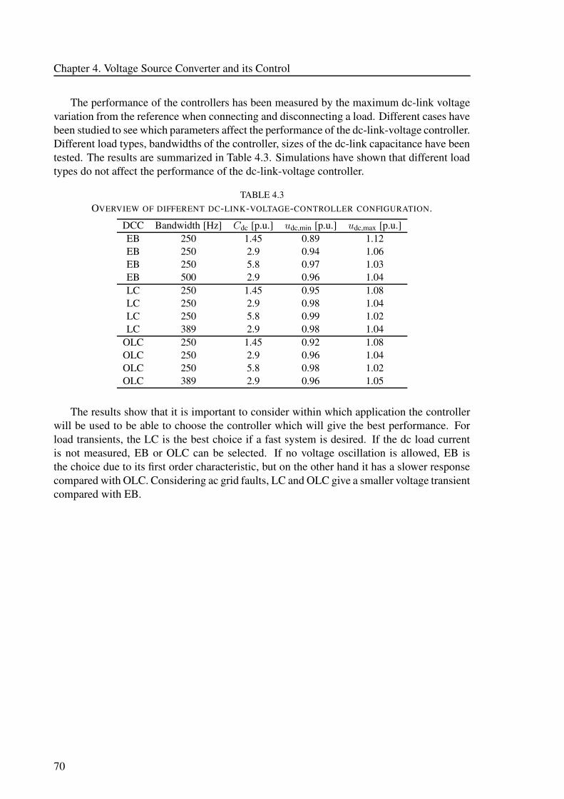
Chapter 4. Voltage Source Converter and its Control
The performance of the controllers has been measured by the maximum dc-link voltagevariation from the reference when connecting and disconnecting a load. Different cases havebeen studied to see which parameters affect the performance of the dc-link-voltage controller.Different load types, bandwidths of the controller, sizes of the dc-link capacitance have beentested. The results are summarized in Table 4.3. Simulations have shown that different loadtypes do not affect the performance of the dc-link-voltage controller.
TABLE 4.3OVERVIEW OF DIFFERENT DC-LINK-VOLTAGE-CONTROLLER CONFIGURATION.
DCC Bandwidth [Hz] Cdc [p.u.] udc,min [p.u.] udc,max [p.u.]EB 250 1.45 0.89 1.12EB 250 2.9 0.94 1.06EB 250 5.8 0.97 1.03EB 500 2.9 0.96 1.04LC 250 1.45 0.95 1.08LC 250 2.9 0.98 1.04LC 250 5.8 0.99 1.02LC 389 2.9 0.98 1.04
OLC 250 1.45 0.92 1.08OLC 250 2.9 0.96 1.04OLC 250 5.8 0.98 1.02OLC 389 2.9 0.96 1.05
The results show that it is important to consider within which application the controllerwill be used to be able to choose the controller which will give the best performance. Forload transients, the LC is the best choice if a fast system is desired. If the dc load currentis not measured, EB or OLC can be selected. If no voltage oscillation is allowed, EB isthe choice due to its first order characteristic, but on the other hand it has a slower responsecompared with OLC. Considering ac grid faults, LC and OLC give a smaller voltage transientcompared with EB.
70
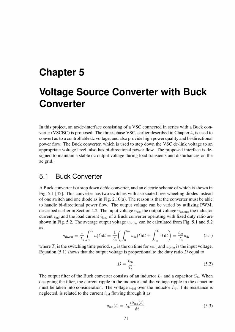
Chapter 5
Voltage Source Converter with BuckConverter
In this project, an ac/dc-interface consisting of a VSC connected in series with a Buck con-verter (VSCBC) is proposed. The three-phase VSC, earlier described in Chapter 4, is used toconvert ac to a controllable dc voltage, and also provide high power quality and bi-directionalpower flow. The Buck converter, which is used to step down the VSC dc-link voltage to anappropriate voltage level, also has bi-directional power flow. The proposed interface is de-signed to maintain a stable dc output voltage during load transients and disturbances on theac grid.
5.1 Buck Converter
A Buck converter is a step down dc/dc converter, and an electric scheme of which is shown inFig. 5.1 [45]. This converter has two switches with associated free-wheeling diodes insteadof one switch and one diode as in Fig. 2.10(a). The reason is that the converter must be ableto handle bi-directional power flow. The output voltage can be varied by utilizing PWM,described earlier in Section 4.2. The input voltage udc, the output voltage udc,out, the inductorcurrent iind and the load current iload of a Buck converter operating with fixed duty ratio areshown in Fig. 5.2. The average output voltage udc,out can be calculated from Fig. 5.1 and 5.2as
udc,out =1
Ts
∫ Ts
0
u(t)dt =1
Ts
(∫ ton
0
udc(t)dt +
∫ Ts
ton
0 dt
)
=ton
Tsudc (5.1)
where Ts is the switching time period, ton is the on time for sw1 and udc,in is the input voltage.Equation (5.1) shows that the output voltage is proportional to the duty ratio D equal to
D =ton
Ts. (5.2)
The output filter of the Buck converter consists of an inductor Lb and a capacitor Cb. Whendesigning the filter, the current ripple in the inductor and the voltage ripple in the capacitormust be taken into consideration. The voltage uind over the inductor Lb, if its resistance isneglected, is related to the current iind flowing through it as
uind(t) = Lbdiind(t)
dt. (5.3)
71
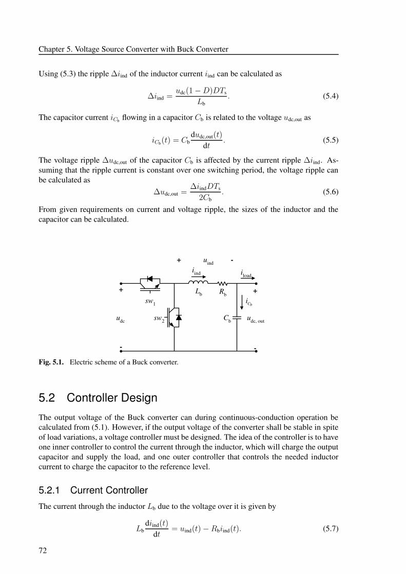
Chapter 5. Voltage Source Converter with Buck Converter
Using (5.3) the ripple ∆iind of the inductor current iind can be calculated as
∆iind =udc(1 − D)DTs
Lb. (5.4)
The capacitor current iCb flowing in a capacitor Cb is related to the voltage udc,out as
iCb(t) = Cbdudc,out(t)
dt. (5.5)
The voltage ripple ∆udc,out of the capacitor Cb is affected by the current ripple ∆iind. As-suming that the ripple current is constant over one switching period, the voltage ripple canbe calculated as
∆udc,out =∆iindDTs
2Cb. (5.6)
From given requirements on current and voltage ripple, the sizes of the inductor and thecapacitor can be calculated.
udc, out
+
-
udc
+
-
iind iload
sw1
sw2
Lb
Cb
Rb
bCi
+ -uind
Fig. 5.1. Electric scheme of a Buck converter.
5.2 Controller Design
The output voltage of the Buck converter can during continuous-conduction operation becalculated from (5.1). However, if the output voltage of the converter shall be stable in spiteof load variations, a voltage controller must be designed. The idea of the controller is to haveone inner controller to control the current through the inductor, which will charge the outputcapacitor and supply the load, and one outer controller that controls the needed inductorcurrent to charge the capacitor to the reference level.
5.2.1 Current Controller
The current through the inductor Lb due to the voltage over it is given by
Lbdiind(t)
dt= uind(t) − Rbiind(t). (5.7)
72
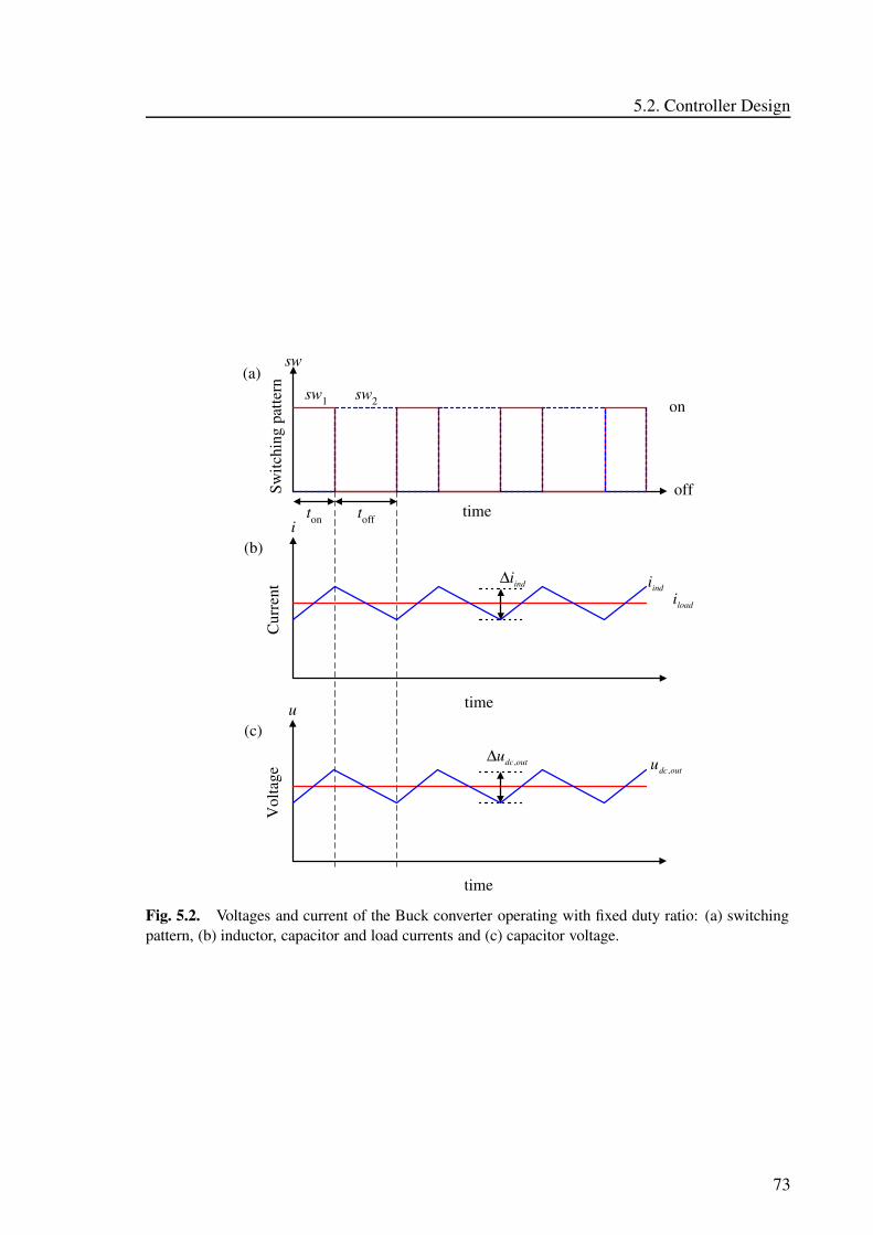
5.2. Controller Design
sw
on
off
loadiindi
timei
time
sw1 sw2
ton toff
indi∆
Cur
rent
Switc
hing
pat
tern
(a)
(b)
u
time
outdcu ,∆
Vol
tage
(c)
outdcu ,
Fig. 5.2. Voltages and current of the Buck converter operating with fixed duty ratio: (a) switchingpattern, (b) inductor, capacitor and load currents and (c) capacitor voltage.
73
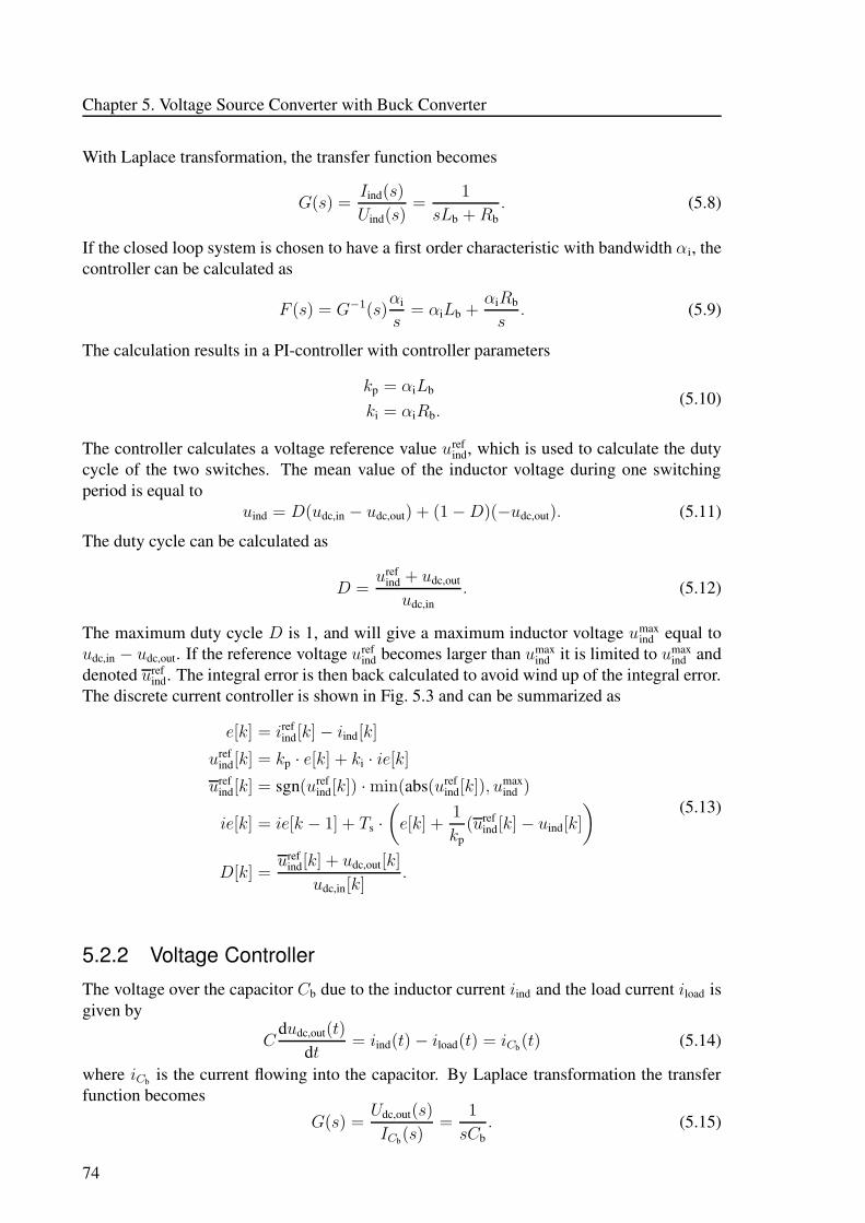
Chapter 5. Voltage Source Converter with Buck Converter
With Laplace transformation, the transfer function becomes
G(s) =Iind(s)
Uind(s)=
1
sLb + Rb. (5.8)
If the closed loop system is chosen to have a first order characteristic with bandwidth αi, thecontroller can be calculated as
F (s) = G−1(s)αi
s= αiLb +
αiRb
s. (5.9)
The calculation results in a PI-controller with controller parameters
kp = αiLb
ki = αiRb.(5.10)
The controller calculates a voltage reference value urefind, which is used to calculate the duty
cycle of the two switches. The mean value of the inductor voltage during one switchingperiod is equal to
uind = D(udc,in − udc,out) + (1 − D)(−udc,out). (5.11)
The duty cycle can be calculated as
D =uref
ind + udc,out
udc,in. (5.12)
The maximum duty cycle D is 1, and will give a maximum inductor voltage umaxind equal to
udc,in − udc,out. If the reference voltage urefind becomes larger than umax
ind it is limited to umaxind and
denoted urefind. The integral error is then back calculated to avoid wind up of the integral error.
The discrete current controller is shown in Fig. 5.3 and can be summarized as
e[k] = irefind[k] − iind[k]
urefind[k] = kp · e[k] + ki · ie[k]
urefind[k] = sgn(uref
ind[k]) · min(abs(urefind[k]), umax
ind )
ie[k] = ie[k − 1] + Ts ·
(
e[k] +1
kp(uref
ind[k] − uind[k]
)
D[k] =uref
ind[k] + udc,out[k]
udc,in[k].
(5.13)
5.2.2 Voltage Controller
The voltage over the capacitor Cb due to the inductor current iind and the load current iload isgiven by
Cdudc,out(t)
dt= iind(t) − iload(t) = iCb(t) (5.14)
where iCb is the current flowing into the capacitor. By Laplace transformation the transferfunction becomes
G(s) =Udc,out(s)
ICb(s)=
1
sCb. (5.15)
74
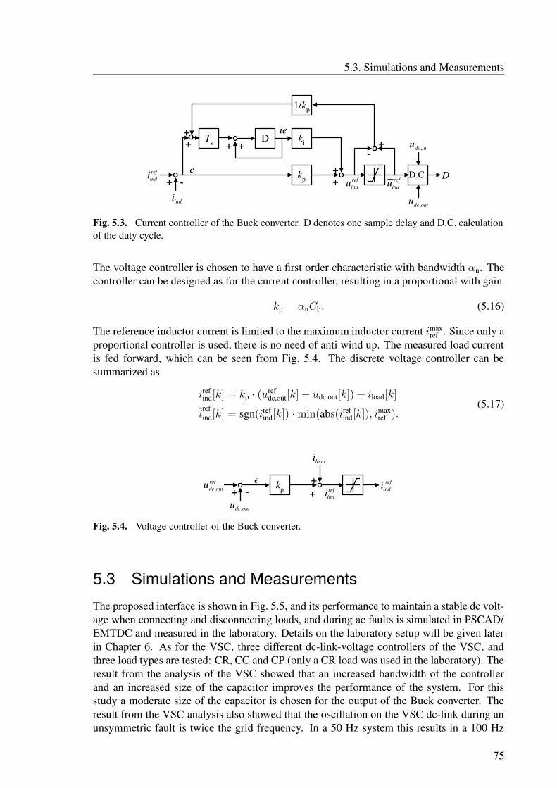
5.3. Simulations and Measurements
1/kp
D kiTs
kp+ -
++
+ +
++
-+
refindi ref
indu refindu
ie
e D
indioutdcu ,
indcu ,
D.C.
Fig. 5.3. Current controller of the Buck converter. D denotes one sample delay and D.C. calculationof the duty cycle.
The voltage controller is chosen to have a first order characteristic with bandwidth αu. Thecontroller can be designed as for the current controller, resulting in a proportional with gain
kp = αuCb. (5.16)
The reference inductor current is limited to the maximum inductor current imaxref . Since only a
proportional controller is used, there is no need of anti wind up. The measured load currentis fed forward, which can be seen from Fig. 5.4. The discrete voltage controller can besummarized as
irefind[k] = kp · (u
refdc,out[k] − udc,out[k]) + iload[k]
irefind[k] = sgn(iref
ind[k]) · min(abs(irefind[k]), imax
ref ).(5.17)
kp+ - ++ref
outdcu , refindi
refindie
outdcu ,
loadi
Fig. 5.4. Voltage controller of the Buck converter.
5.3 Simulations and Measurements
The proposed interface is shown in Fig. 5.5, and its performance to maintain a stable dc volt-age when connecting and disconnecting loads, and during ac faults is simulated in PSCAD/EMTDC and measured in the laboratory. Details on the laboratory setup will be given laterin Chapter 6. As for the VSC, three different dc-link-voltage controllers of the VSC, andthree load types are tested: CR, CC and CP (only a CR load was used in the laboratory). Theresult from the analysis of the VSC showed that an increased bandwidth of the controllerand an increased size of the capacitor improves the performance of the system. For thisstudy a moderate size of the capacitor is chosen for the output of the Buck converter. Theresult from the VSC analysis also showed that the oscillation on the VSC dc-link during anunsymmetric fault is twice the grid frequency. In a 50 Hz system this results in a 100 Hz
75
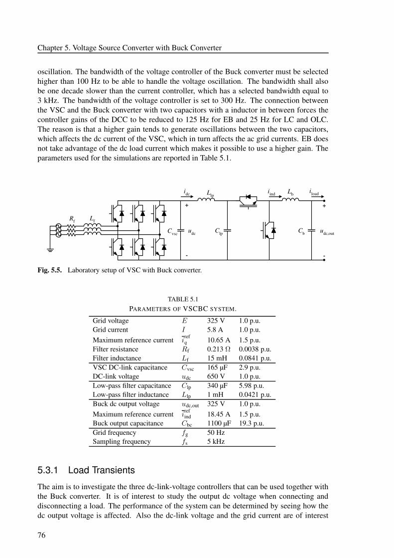
Chapter 5. Voltage Source Converter with Buck Converter
oscillation. The bandwidth of the voltage controller of the Buck converter must be selectedhigher than 100 Hz to be able to handle the voltage oscillation. The bandwidth shall alsobe one decade slower than the current controller, which has a selected bandwidth equal to3 kHz. The bandwidth of the voltage controller is set to 300 Hz. The connection betweenthe VSC and the Buck converter with two capacitors with a inductor in between forces thecontroller gains of the DCC to be reduced to 125 Hz for EB and 25 Hz for LC and OLC.The reason is that a higher gain tends to generate oscillations between the two capacitors,which affects the dc current of the VSC, which in turn affects the ac grid currents. EB doesnot take advantage of the dc load current which makes it possible to use a higher gain. Theparameters used for the simulations are reported in Table 5.1.
+
-
Rf Lf
Lb
udc
+
-
udc,out
idc iind iload
CbClp
Llp
Cvsc
Fig. 5.5. Laboratory setup of VSC with Buck converter.
TABLE 5.1PARAMETERS OF VSCBC SYSTEM.
Grid voltage E 325 V 1.0 p.u.Grid current I 5.8 A 1.0 p.u.Maximum reference current i
refq 10.65 A 1.5 p.u.
Filter resistance Rf 0.213 Ω 0.0038 p.u.Filter inductance Lf 15 mH 0.0841 p.u.VSC DC-link capacitance Cvsc 165 µF 2.9 p.u.DC-link voltage udc 650 V 1.0 p.u.Low-pass filter capacitance Clp 340 µF 5.98 p.u.Low-pass filter inductance Llp 1 mH 0.0421 p.u.Buck dc output voltage udc,out 325 V 1.0 p.u.Maximum reference current i
refind 18.45 A 1.5 p.u.
Buck output capacitance Cbc 1100 µF 19.3 p.u.Grid frequency fg 50 HzSampling frequency fs 5 kHz
5.3.1 Load Transients
The aim is to investigate the three dc-link-voltage controllers that can be used together withthe Buck converter. It is of interest to study the output dc voltage when connecting anddisconnecting a load. The performance of the system can be determined by seeing how thedc output voltage is affected. Also the dc-link voltage and the grid current are of interest
76
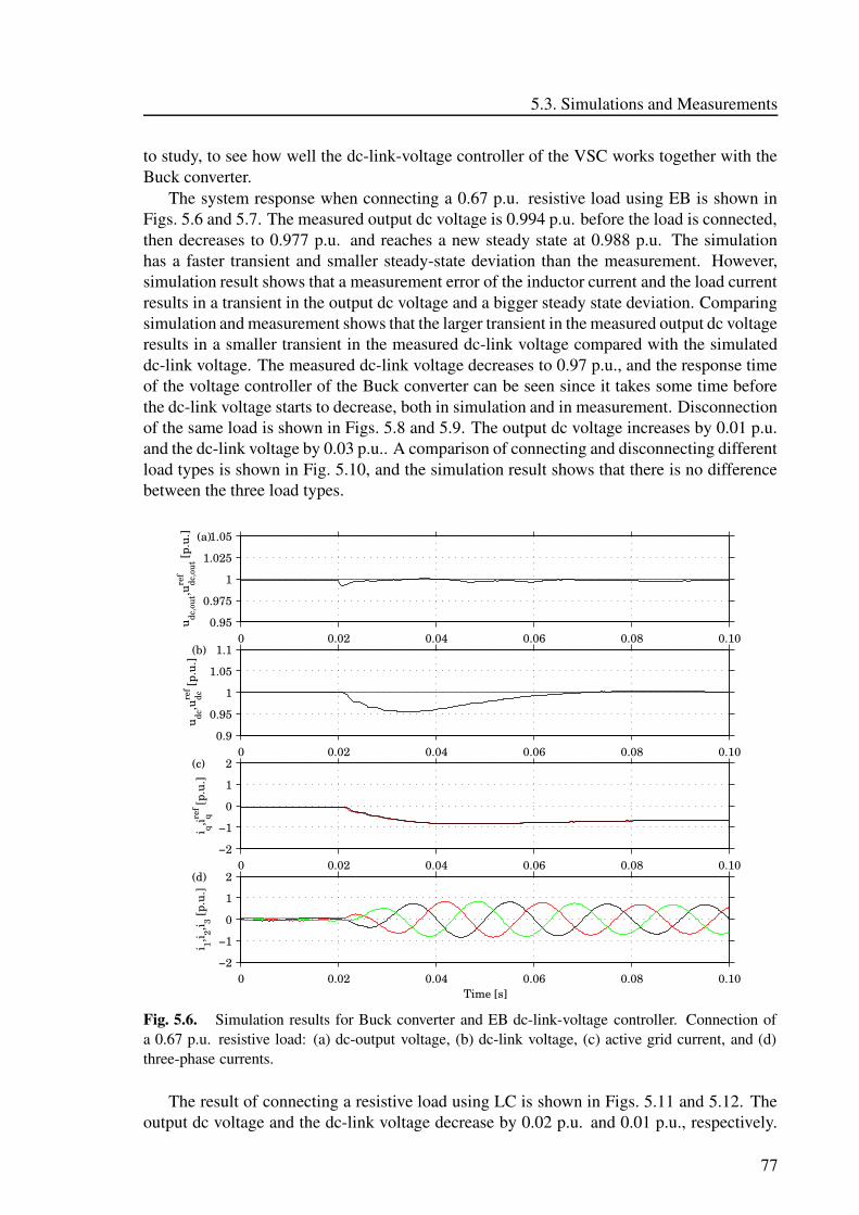
5.3. Simulations and Measurements
to study, to see how well the dc-link-voltage controller of the VSC works together with theBuck converter.
The system response when connecting a 0.67 p.u. resistive load using EB is shown inFigs. 5.6 and 5.7. The measured output dc voltage is 0.994 p.u. before the load is connected,then decreases to 0.977 p.u. and reaches a new steady state at 0.988 p.u. The simulationhas a faster transient and smaller steady-state deviation than the measurement. However,simulation result shows that a measurement error of the inductor current and the load currentresults in a transient in the output dc voltage and a bigger steady state deviation. Comparingsimulation and measurement shows that the larger transient in the measured output dc voltageresults in a smaller transient in the measured dc-link voltage compared with the simulateddc-link voltage. The measured dc-link voltage decreases to 0.97 p.u., and the response timeof the voltage controller of the Buck converter can be seen since it takes some time beforethe dc-link voltage starts to decrease, both in simulation and in measurement. Disconnectionof the same load is shown in Figs. 5.8 and 5.9. The output dc voltage increases by 0.01 p.u.and the dc-link voltage by 0.03 p.u.. A comparison of connecting and disconnecting differentload types is shown in Fig. 5.10, and the simulation result shows that there is no differencebetween the three load types.
0 0.02 0.04 0.06 0.08 0.100.95
0.975
1
1.025
1.05
u dc,o
ut,u
dc,o
utre
f [p
.u.] (a)
0 0.02 0.04 0.06 0.08 0.100.9
0.95
1
1.05
1.1
u dc,u
dcref [p
.u.]
(b)
0 0.02 0.04 0.06 0.08 0.10−2
−1
0
1
2
i q,i qref [p
.u.]
(c)
0 0.02 0.04 0.06 0.08 0.10−2
−1
0
1
2
Time [s]
i 1,i 2,i 3 [p.u
.]
(d)
Fig. 5.6. Simulation results for Buck converter and EB dc-link-voltage controller. Connection ofa 0.67 p.u. resistive load: (a) dc-output voltage, (b) dc-link voltage, (c) active grid current, and (d)three-phase currents.
The result of connecting a resistive load using LC is shown in Figs. 5.11 and 5.12. Theoutput dc voltage and the dc-link voltage decrease by 0.02 p.u. and 0.01 p.u., respectively.
77
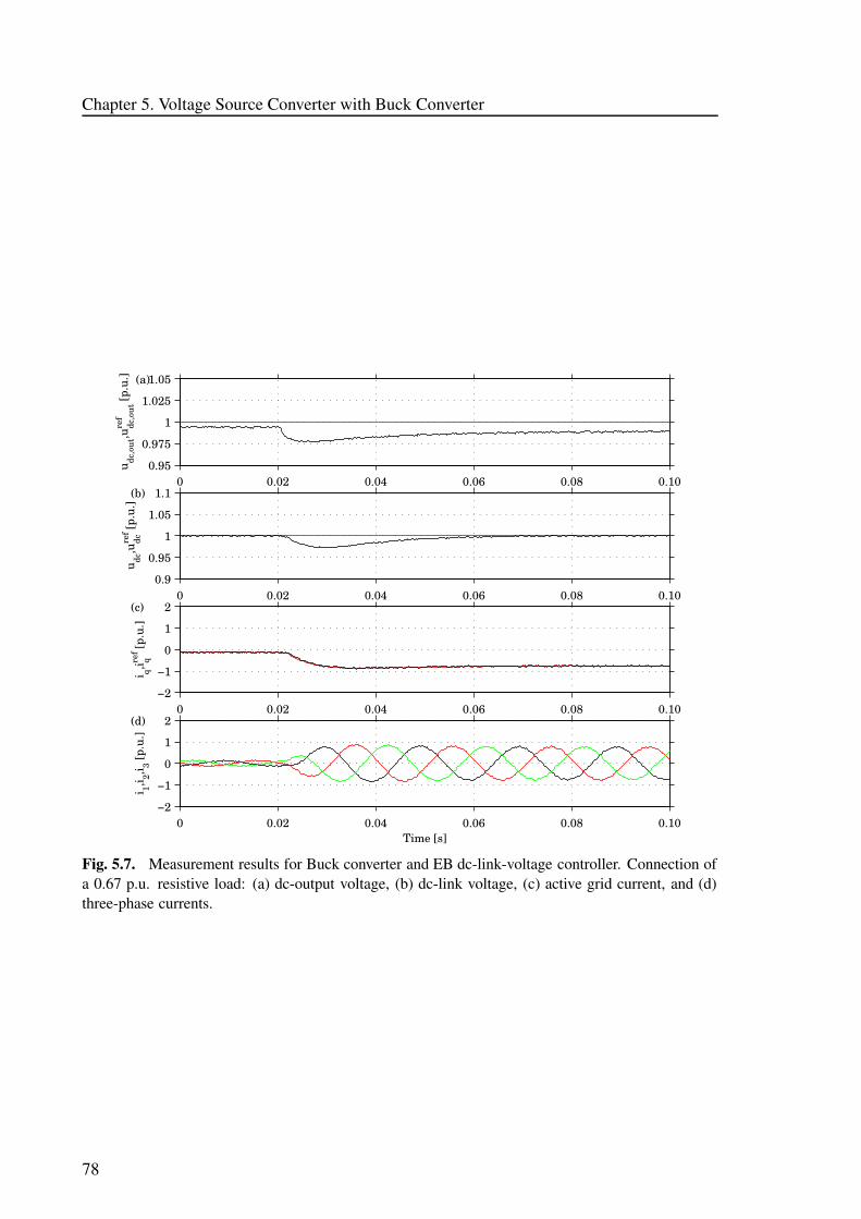
Chapter 5. Voltage Source Converter with Buck Converter
0 0.02 0.04 0.06 0.08 0.100.95
0.975
1
1.025
1.05
u dc,o
ut,u
dc,o
utre
f [p
.u.] (a)
0 0.02 0.04 0.06 0.08 0.100.9
0.95
1
1.05
1.1
u dc,u
dcref [p
.u.]
(b)
0 0.02 0.04 0.06 0.08 0.10−2
−1
0
1
2
i q,i qref [p
.u.]
(c)
0 0.02 0.04 0.06 0.08 0.10−2
−1
0
1
2
Time [s]
i 1,i 2,i 3 [p.u
.]
(d)
Fig. 5.7. Measurement results for Buck converter and EB dc-link-voltage controller. Connection ofa 0.67 p.u. resistive load: (a) dc-output voltage, (b) dc-link voltage, (c) active grid current, and (d)three-phase currents.
78
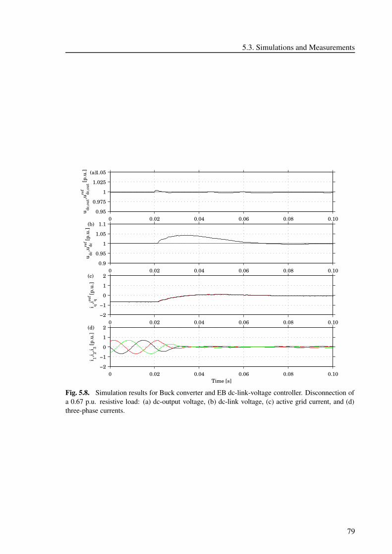
5.3. Simulations and Measurements
0 0.02 0.04 0.06 0.08 0.100.95
0.975
1
1.025
1.05
u dc,o
ut,u
dc,o
utre
f [p
.u.] (a)
0 0.02 0.04 0.06 0.08 0.100.9
0.95
1
1.05
1.1
u dc,u
dcref [p
.u.]
(b)
0 0.02 0.04 0.06 0.08 0.10−2
−1
0
1
2
i q,i qref [p
.u.]
(c)
0 0.02 0.04 0.06 0.08 0.10−2
−1
0
1
2
Time [s]
i 1,i 2,i 3 [p.u
.]
(d)
Fig. 5.8. Simulation results for Buck converter and EB dc-link-voltage controller. Disconnection ofa 0.67 p.u. resistive load: (a) dc-output voltage, (b) dc-link voltage, (c) active grid current, and (d)three-phase currents.
79
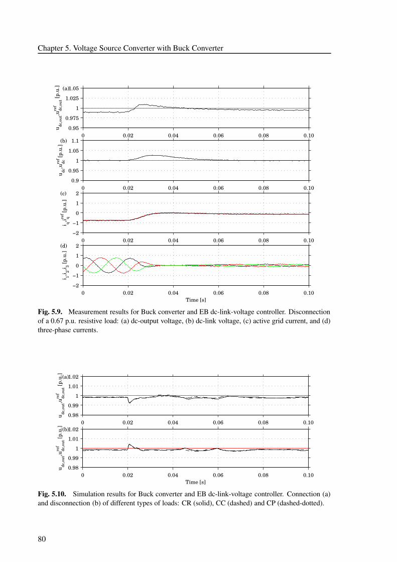
Chapter 5. Voltage Source Converter with Buck Converter
0 0.02 0.04 0.06 0.08 0.100.95
0.975
1
1.025
1.05
u dc,o
ut,u
dc,o
utre
f [p
.u.] (a)
0 0.02 0.04 0.06 0.08 0.100.9
0.95
1
1.05
1.1
u dc,u
dcref [p
.u.]
(b)
0 0.02 0.04 0.06 0.08 0.10−2
−1
0
1
2
i q,i qref [p
.u.]
(c)
0 0.02 0.04 0.06 0.08 0.10−2
−1
0
1
2
Time [s]
i 1,i 2,i 3 [p.u
.]
(d)
Fig. 5.9. Measurement results for Buck converter and EB dc-link-voltage controller. Disconnectionof a 0.67 p.u. resistive load: (a) dc-output voltage, (b) dc-link voltage, (c) active grid current, and (d)three-phase currents.
0 0.02 0.04 0.06 0.08 0.100.98
0.99
1
1.01
1.02
u dc,o
ut,u
dc,o
utre
f [p
.u.] (a)
0 0.02 0.04 0.06 0.08 0.100.98
0.99
1
1.01
1.02
u dc,o
ut,u
dc,o
utre
f [p
.u.] (b)
Time [s]
Fig. 5.10. Simulation results for Buck converter and EB dc-link-voltage controller. Connection (a)and disconnection (b) of different types of loads: CR (solid), CC (dashed) and CP (dashed-dotted).
80
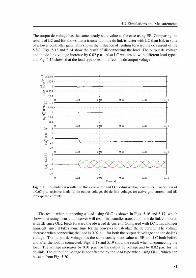
5.3. Simulations and Measurements
The output dc voltage has the same steady-state value as the case using EB. Comparing theresults of LC and EB shows that a transient on the dc link is faster with LC than EB, in spiteof a lower controller gain. This shows the influence of feeding forward the dc current of theVSC. Figs. 5.13 and 5.14 show the result of disconnecting the load. The output dc voltageand the dc-link voltage increase by 0.02 p.u.. Also LC was tested with different load types,and Fig. 5.15 shows that the load type does not affect the dc output voltage.
0 0.02 0.04 0.06 0.08 0.100.95
0.975
1
1.025
1.05
u dc,o
ut,u
dc,o
utre
f [p
.u.] (a)
0 0.02 0.04 0.06 0.08 0.100.9
0.95
1
1.05
1.1
u dc,u
dcref [p
.u.]
(b)
0 0.02 0.04 0.06 0.08 0.10−2
−1
0
1
2
i q,i qref [p
.u.]
(c)
0 0.02 0.04 0.06 0.08 0.10−2
−1
0
1
2
Time [s]
i 1,i 2,i 3 [p.u
.]
(d)
Fig. 5.11. Simulation results for Buck converter and LC dc-link-voltage controller. Connection ofa 0.67 p.u. resistive load: (a) dc-output voltage, (b) dc-link voltage, (c) active grid current, and (d)three-phase currents.
The result when connecting a load using OLC is shown in Figs. 5.16 and 5.17, whichshows that using a current observer will result in a smaller transient on the dc link comparedwith EB since OLC feeds forward the observed dc current. Compared with LC it has a longertransient, since it takes some time for the observer to calculate the dc current. The voltagedecrease when connecting the load is 0.02 p.u. for both the output dc voltage and the dc-linkvoltage. The output dc voltage has the same steady-state value as EB and LC both beforeand after the load is connected. Figs. 5.18 and 5.19 show the result when disconnecting theload. The voltage increases by 0.01 p.u. for the output dc voltage and by 0.02 p.u. for thedc-link. The output dc voltage is not affected by the load type when using OLC, which canbe seen from Fig. 5.20.
81
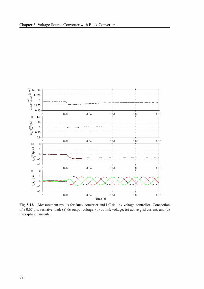
Chapter 5. Voltage Source Converter with Buck Converter
0 0.02 0.04 0.06 0.08 0.100.95
0.975
1
1.025
1.05
u dc,o
ut,u
dc,o
utre
f [p
.u.] (a)
0 0.02 0.04 0.06 0.08 0.100.9
0.95
1
1.05
1.1
u dc,u
dcref [p
.u.]
(b)
0 0.02 0.04 0.06 0.08 0.10−2
−1
0
1
2
i q,i qref [p
.u.]
(c)
0 0.02 0.04 0.06 0.08 0.10−2
−1
0
1
2
Time [s]
i 1,i 2,i 3 [p.u
.]
(d)
Fig. 5.12. Measurement results for Buck converter and LC dc-link-voltage controller. Connectionof a 0.67 p.u. resistive load: (a) dc-output voltage, (b) dc-link voltage, (c) active grid current, and (d)three-phase currents.
82
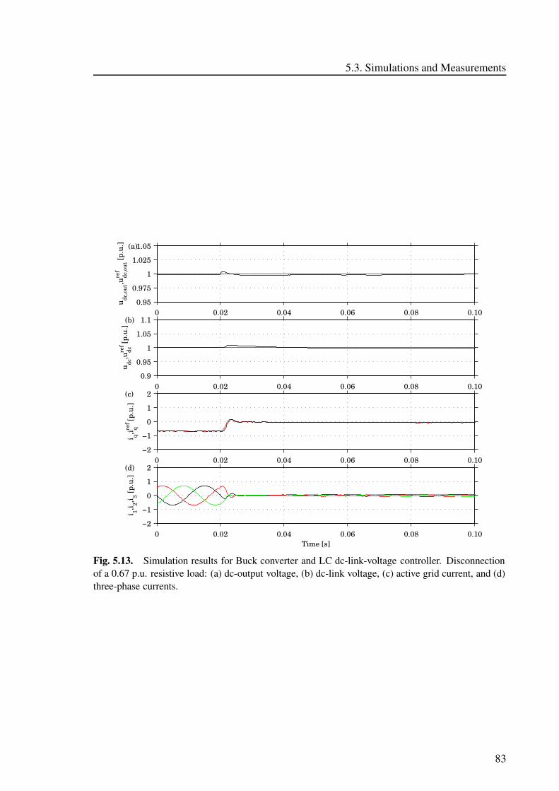
5.3. Simulations and Measurements
0 0.02 0.04 0.06 0.08 0.100.95
0.975
1
1.025
1.05
u dc,o
ut,u
dc,o
utre
f [p
.u.] (a)
0 0.02 0.04 0.06 0.08 0.100.9
0.95
1
1.05
1.1
u dc,u
dcref [p
.u.]
(b)
0 0.02 0.04 0.06 0.08 0.10−2
−1
0
1
2
i q,i qref [p
.u.]
(c)
0 0.02 0.04 0.06 0.08 0.10−2
−1
0
1
2
Time [s]
i 1,i 2,i 3 [p.u
.]
(d)
Fig. 5.13. Simulation results for Buck converter and LC dc-link-voltage controller. Disconnectionof a 0.67 p.u. resistive load: (a) dc-output voltage, (b) dc-link voltage, (c) active grid current, and (d)three-phase currents.
83
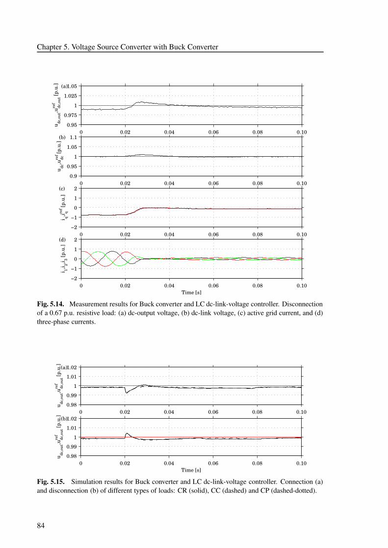
Chapter 5. Voltage Source Converter with Buck Converter
0 0.02 0.04 0.06 0.08 0.100.95
0.975
1
1.025
1.05
u dc,o
ut,u
dc,o
utre
f [p
.u.] (a)
0 0.02 0.04 0.06 0.08 0.100.9
0.95
1
1.05
1.1
u dc,u
dcref [p
.u.]
(b)
0 0.02 0.04 0.06 0.08 0.10−2
−1
0
1
2
i q,i qref [p
.u.]
(c)
0 0.02 0.04 0.06 0.08 0.10−2
−1
0
1
2
Time [s]
i 1,i 2,i 3 [p.u
.]
(d)
Fig. 5.14. Measurement results for Buck converter and LC dc-link-voltage controller. Disconnectionof a 0.67 p.u. resistive load: (a) dc-output voltage, (b) dc-link voltage, (c) active grid current, and (d)three-phase currents.
0 0.02 0.04 0.06 0.08 0.100.98
0.99
1
1.01
1.02
u dc,o
ut,u
dc,o
utre
f [p
.u.] (a)
0 0.02 0.04 0.06 0.08 0.100.98
0.99
1
1.01
1.02
u dc,o
ut,u
dc,o
utre
f [p
.u.] (b)
Time [s]
Fig. 5.15. Simulation results for Buck converter and LC dc-link-voltage controller. Connection (a)and disconnection (b) of different types of loads: CR (solid), CC (dashed) and CP (dashed-dotted).
84
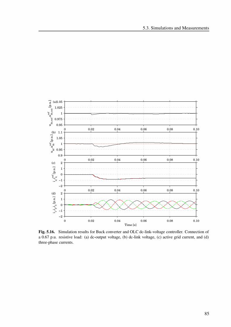
5.3. Simulations and Measurements
0 0.02 0.04 0.06 0.08 0.100.95
0.975
1
1.025
1.05
u dc,o
ut,u
dc,o
utre
f [p
.u.] (a)
0 0.02 0.04 0.06 0.08 0.100.9
0.95
1
1.05
1.1
u dc,u
dcref [p
.u.]
(b)
0 0.02 0.04 0.06 0.08 0.10−2
−1
0
1
2
i q,i qref [p
.u.]
(c)
0 0.02 0.04 0.06 0.08 0.10−2
−1
0
1
2
Time [s]
i 1,i 2,i 3 [p.u
.]
(d)
Fig. 5.16. Simulation results for Buck converter and OLC dc-link-voltage controller. Connection ofa 0.67 p.u. resistive load: (a) dc-output voltage, (b) dc-link voltage, (c) active grid current, and (d)three-phase currents.
85
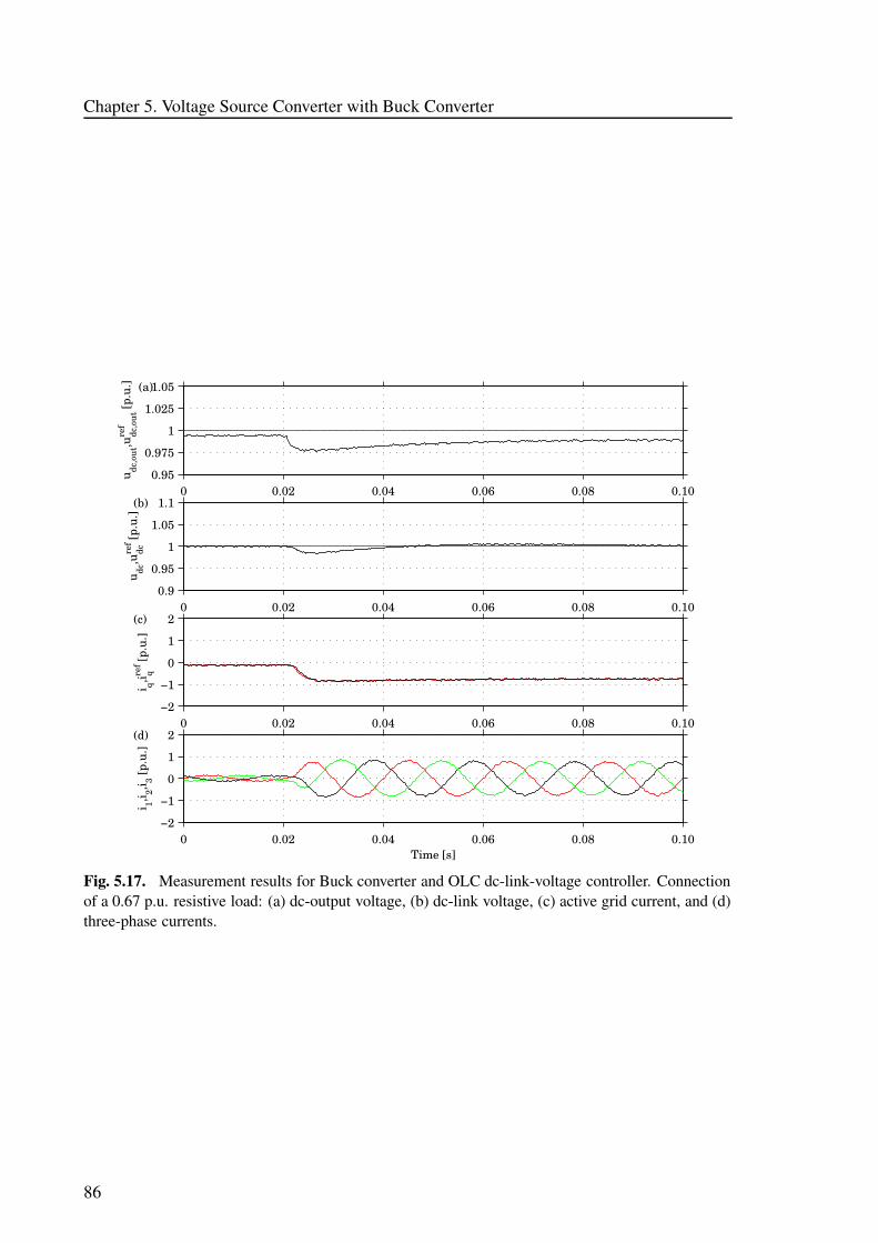
Chapter 5. Voltage Source Converter with Buck Converter
0 0.02 0.04 0.06 0.08 0.100.95
0.975
1
1.025
1.05
u dc,o
ut,u
dc,o
utre
f [p
.u.] (a)
0 0.02 0.04 0.06 0.08 0.100.9
0.95
1
1.05
1.1
u dc,u
dcref [p
.u.]
(b)
0 0.02 0.04 0.06 0.08 0.10−2
−1
0
1
2
i q,i qref [p
.u.]
(c)
0 0.02 0.04 0.06 0.08 0.10−2
−1
0
1
2
Time [s]
i 1,i 2,i 3 [p.u
.]
(d)
Fig. 5.17. Measurement results for Buck converter and OLC dc-link-voltage controller. Connectionof a 0.67 p.u. resistive load: (a) dc-output voltage, (b) dc-link voltage, (c) active grid current, and (d)three-phase currents.
86
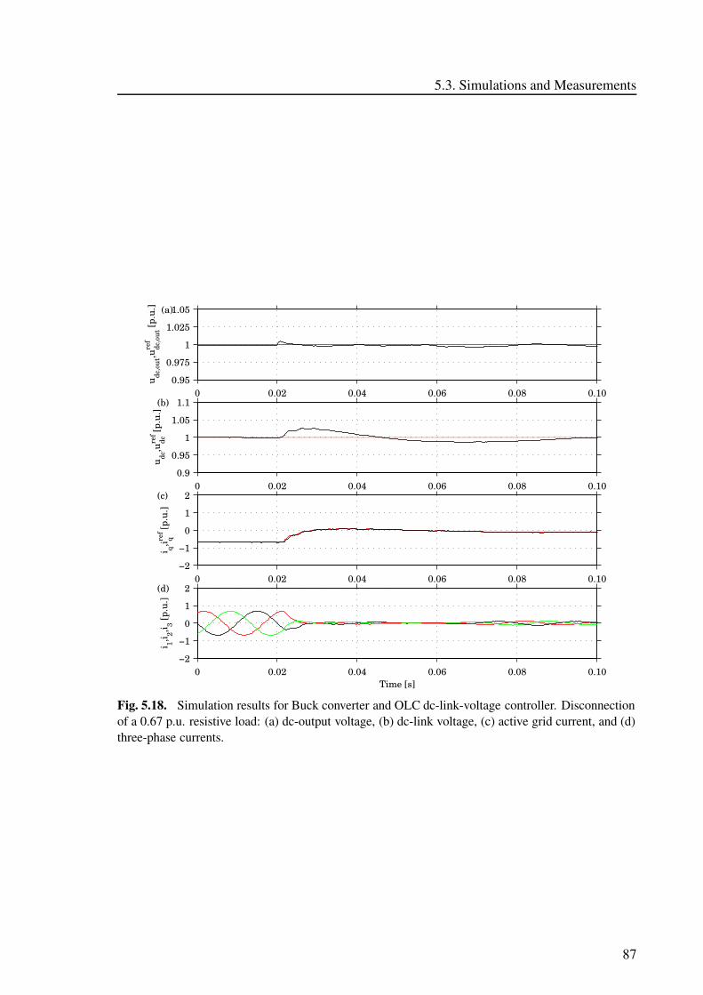
5.3. Simulations and Measurements
0 0.02 0.04 0.06 0.08 0.100.95
0.975
1
1.025
1.05
u dc,o
ut,u
dc,o
utre
f [p
.u.] (a)
0 0.02 0.04 0.06 0.08 0.100.9
0.95
1
1.05
1.1
u dc,u
dcref [p
.u.]
(b)
0 0.02 0.04 0.06 0.08 0.10−2
−1
0
1
2
i q,i qref [p
.u.]
(c)
0 0.02 0.04 0.06 0.08 0.10−2
−1
0
1
2
Time [s]
i 1,i 2,i 3 [p.u
.]
(d)
Fig. 5.18. Simulation results for Buck converter and OLC dc-link-voltage controller. Disconnectionof a 0.67 p.u. resistive load: (a) dc-output voltage, (b) dc-link voltage, (c) active grid current, and (d)three-phase currents.
87
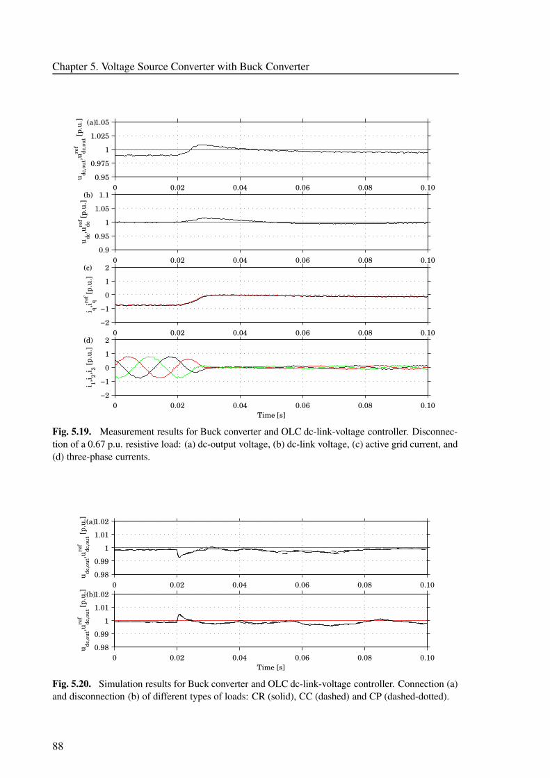
Chapter 5. Voltage Source Converter with Buck Converter
0 0.02 0.04 0.06 0.08 0.100.95
0.975
1
1.025
1.05
u dc,o
ut,u
dc,o
utre
f [p
.u.] (a)
0 0.02 0.04 0.06 0.08 0.100.9
0.95
1
1.05
1.1
u dc,u
dcref [p
.u.]
(b)
0 0.02 0.04 0.06 0.08 0.10−2
−1
0
1
2
i q,i qref [p
.u.]
(c)
0 0.02 0.04 0.06 0.08 0.10−2
−1
0
1
2
Time [s]
i 1,i 2,i 3 [p.u
.]
(d)
Fig. 5.19. Measurement results for Buck converter and OLC dc-link-voltage controller. Disconnec-tion of a 0.67 p.u. resistive load: (a) dc-output voltage, (b) dc-link voltage, (c) active grid current, and(d) three-phase currents.
0 0.02 0.04 0.06 0.08 0.100.98
0.99
1
1.01
1.02
u dc,o
ut,u
dc,o
utre
f [p
.u.] (a)
0 0.02 0.04 0.06 0.08 0.100.98
0.99
1
1.01
1.02
u dc,o
ut,u
dc,o
utre
f [p
.u.] (b)
Time [s]
Fig. 5.20. Simulation results for Buck converter and OLC dc-link-voltage controller. Connection (a)and disconnection (b) of different types of loads: CR (solid), CC (dashed) and CP (dashed-dotted).
88

5.4. Conclusions
5.3.2 Disturbances
The system performance during disturbances on the ac grid is simulated and verified in thelaboratory setup. As long as the output voltage of the VSC is higher than the desired outputvoltage of the Buck converter, and the output voltage of the VSC does not vary faster thanthe voltage controller of the Buck converter can follow, the output voltage can be maintainedat the reference level. According to (4.27), the minimum retained grid voltage is determinedby the maximum current that the VSC can handle. The system has been tested with a phase-to-phase fault with 0.75 p.u. retained voltage, 12 % unbalance, and 12° phase-angle jumpin the simulation. In the laboratory it was a phase-to-phase fault with 0.79 p.u. retainedvoltage during 0.07 s, and with 27% unbalance and 11° phase-angle jump [68]. The smallerphase-angle jump will be seen as a smaller transient in the dc-link voltage and the higherunbalance as a higher oscillation in the dc-link voltage and the currents. To be able to makethe fault in the laboratory, a weak ac grid was used, which is explained later in Chapter 6,and the gain of the VCC was therefore reduced to 70 % times dead-beat gain. The gain forEB was reduced to 125 Hz and for LC and OLC to 25 Hz. Due to the reduced gain only a0.47 p.u. resistive load could be used.
The simulation results using EB, LC and OLC are shown in Figs. 5.21, 5.23 and 5.25,and the corresponding measurements are shown in Figs. 5.22, 5.24 and 5.26. All three con-trollers result in an oscillating dc-link voltage. The voltage controller of the Buck convertercan follow the oscillation and the output voltage is unaffected. Practical limitations in thelaboratory made it impossible to make faults which are close to the operation limit of con-verter. A simulation with a single-phase fault with 0.1 p.u. retained voltage is shown inFig. 5.27, which clearly shows that the steady-state oscillation on the dc link does not affectthe output dc voltage.
5.4 Conclusions
In this chapter, a proposed ac/dc interface consisting of a VSC and a Buck converter in serieshas been analyzed, simulated and tested in the laboratory. The results show that this interfaceis suitable to convert ac to an appropriate dc voltage. The performance of the system has beenstudied during connection/disconnection of loads and during disturbances on the ac grid, andthe influence of the dc-link-voltage controller has been studied. Simulation results show thatusing LC will result in an oscillation of the dc-link voltage when the load is connected. Theload step generates a current flowing between the dc-link capacitor and the low-pass-filtercapacitor, and this current affects the LC and results in distorted grid currents. EB and OLC,which both do not measure the dc current, have a better transient response.
The system was also studied during an unsymmetrical disturbance on the ac grid, andsimulations show that the output voltage of the Buck converter is not affected by the distur-bance.
The conclusion is that the EB or OLC are preferable to use in a setup consisting of oneVSC and one Buck converter. The fact that the EB is slower than the OLC does not affectthe output voltage, as long as the dc-link voltage is higher than the output voltage.
89

Chapter 5. Voltage Source Converter with Buck Converter
0 0.03 0.06 0.09 0.12 0.15−2
−1
0
1
2
Time [s]
e 1,e2,e
3 [p.u
.]
(a)
0 0.03 0.06 0.09 0.12 0.150.95
0.975
1
1.025
1.05
u dc,u
dcref [p
.u.]
(b)
0 0.03 0.06 0.09 0.12 0.150.95
0.975
1
1.025
1.05
u dc,o
ut,u
dc,o
utre
f [p
.u.] (c)
0 0.03 0.06 0.09 0.12 0.15−2
−1.5
−1
−0.5
0
i q,i qref [p
.u.]
(d)
Time [s]
Fig. 5.21. Simulation results for Buck converter and EB during phase-to-phase fault: (a) gridvoltages, (b) dc-link voltage, (c) dc output voltage, and (d) active grid current.
90

5.4. Conclusions
0 0.03 0.06 0.09 0.12 0.15−2
−1
0
1
2
e 1,e2,e
3 [p.u
.]
(a)
0 0.03 0.06 0.09 0.12 0.150.95
0.975
1
1.025
1.05
u dc,u
dcref [p
.u.]
(b)
0 0.03 0.06 0.09 0.12 0.150.95
0.975
1
1.025
1.05
u dc,o
ut,u
dc,o
utre
f [p
.u.] (c)
0 0.02 0.04 0.06 0.08 0.10−2
−1.5
−1
−0.5
0
i q,i qref [p
.u.]
(d)
Time [s]
Fig. 5.22. Measurement results for Buck converter and EB during phase-to-phase fault: (a) gridvoltages, (b) dc-link voltage, (c) dc output voltage, and (d) active grid current.
91
Chapter 5. Voltage Source Converter with Buck Converter
0 0.03 0.06 0.09 0.12 0.15−2
−1
0
1
2
Time [s]
e 1,e2,e
3 [p.u
.]
(a)
0 0.03 0.06 0.09 0.12 0.150.95
0.975
1
1.025
1.05
u dc,u
dcref [p
.u.]
(b)
0 0.03 0.06 0.09 0.12 0.150.95
0.975
1
1.025
1.05
u dc,o
ut,u
dc,o
utre
f [p
.u.] (c)
0 0.03 0.06 0.09 0.12 0.15−2
−1.5
−1
−0.5
0
i q,i qref [p
.u.]
(d)
Time [s]
Fig. 5.23. Simulation results for Buck converter and LC during phase-to-phase fault: (a) gridvoltages, (b) dc-link voltage, (c) dc output voltage, and (d) active grid current.
92

5.4. Conclusions
0 0.03 0.06 0.09 0.12 0.15−2
−1
0
1
2
e 1,e2,e
3 [p.u
.]
(a)
0 0.03 0.06 0.09 0.12 0.150.95
0.975
1
1.025
1.05
u dc,u
dcref [p
.u.]
(b)
0 0.03 0.06 0.09 0.12 0.150.95
0.975
1
1.025
1.05
u dc,o
ut,u
dc,o
utre
f [p
.u.] (c)
0 0.02 0.04 0.06 0.08 0.10−2
−1.5
−1
−0.5
0
i q,i qref [p
.u.]
(d)
Time [s]
Fig. 5.24. Measurement results for Buck converter and LC during phase-to-phase fault: (a) gridvoltages, (b) dc-link voltage, (c) dc output voltage, and (d) active grid current.
93
Chapter 5. Voltage Source Converter with Buck Converter
0 0.03 0.06 0.09 0.12 0.15−2
−1
0
1
2
Time [s]
e 1,e2,e
3 [p.u
.]
(a)
0 0.03 0.06 0.09 0.12 0.150.95
0.975
1
1.025
1.05
u dc,u
dcref [p
.u.]
(b)
0 0.03 0.06 0.09 0.12 0.150.95
0.975
1
1.025
1.05
u dc,o
ut,u
dc,o
utre
f [p
.u.] (c)
0 0.03 0.06 0.09 0.12 0.15−2
−1.5
−1
−0.5
0
i q,i qref [p
.u.]
(d)
Time [s]
Fig. 5.25. Simulation results for Buck converter and OLC during phase-to-phase fault: (a) gridvoltages, (b) dc-link voltage, (c) dc output voltage, and (d) active grid current.
94
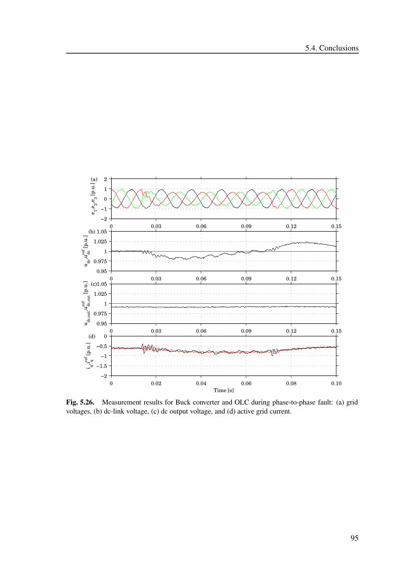
5.4. Conclusions
0 0.03 0.06 0.09 0.12 0.15−2
−1
0
1
2
e 1,e2,e
3 [p.u
.]
(a)
0 0.03 0.06 0.09 0.12 0.150.95
0.975
1
1.025
1.05
u dc,u
dcref [p
.u.]
(b)
0 0.03 0.06 0.09 0.12 0.150.95
0.975
1
1.025
1.05
u dc,o
ut,u
dc,o
utre
f [p
.u.] (c)
0 0.02 0.04 0.06 0.08 0.10−2
−1.5
−1
−0.5
0
i q,i qref [p
.u.]
(d)
Time [s]
Fig. 5.26. Measurement results for Buck converter and OLC during phase-to-phase fault: (a) gridvoltages, (b) dc-link voltage, (c) dc output voltage, and (d) active grid current.
95
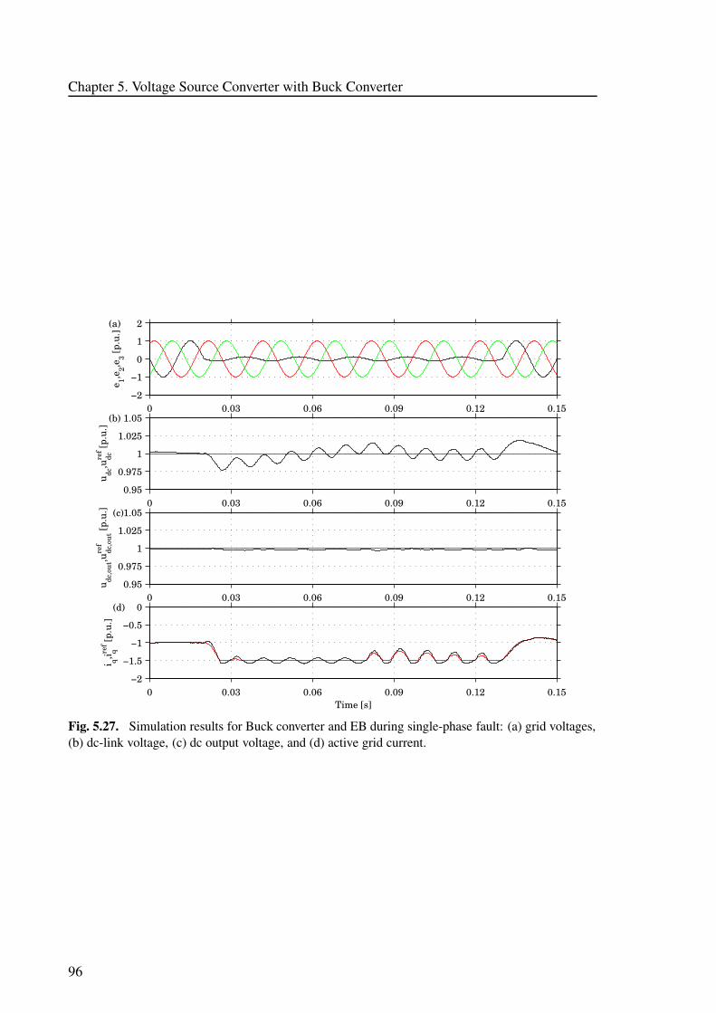
Chapter 5. Voltage Source Converter with Buck Converter
0 0.03 0.06 0.09 0.12 0.15−2
−1
0
1
2
Time [s]
e 1,e2,e
3 [p.u
.]
(a)
0 0.03 0.06 0.09 0.12 0.150.95
0.975
1
1.025
1.05
u dc,u
dcref [p
.u.]
(b)
0 0.03 0.06 0.09 0.12 0.150.95
0.975
1
1.025
1.05
u dc,o
ut,u
dc,o
utre
f [p
.u.] (c)
0 0.03 0.06 0.09 0.12 0.15−2
−1.5
−1
−0.5
0
i q,i qref [p
.u.]
(d)
Time [s]
Fig. 5.27. Simulation results for Buck converter and EB during single-phase fault: (a) grid voltages,(b) dc-link voltage, (c) dc output voltage, and (d) active grid current.
96
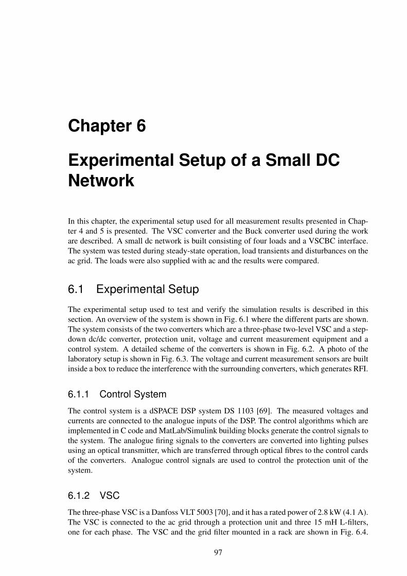
Chapter 6
Experimental Setup of a Small DCNetwork
In this chapter, the experimental setup used for all measurement results presented in Chap-ter 4 and 5 is presented. The VSC converter and the Buck converter used during the workare described. A small dc network is built consisting of four loads and a VSCBC interface.The system was tested during steady-state operation, load transients and disturbances on theac grid. The loads were also supplied with ac and the results were compared.
6.1 Experimental Setup
The experimental setup used to test and verify the simulation results is described in thissection. An overview of the system is shown in Fig. 6.1 where the different parts are shown.The system consists of the two converters which are a three-phase two-level VSC and a step-down dc/dc converter, protection unit, voltage and current measurement equipment and acontrol system. A detailed scheme of the converters is shown in Fig. 6.2. A photo of thelaboratory setup is shown in Fig. 6.3. The voltage and current measurement sensors are builtinside a box to reduce the interference with the surrounding converters, which generates RFI.
6.1.1 Control System
The control system is a dSPACE DSP system DS 1103 [69]. The measured voltages andcurrents are connected to the analogue inputs of the DSP. The control algorithms which areimplemented in C code and MatLab/Simulink building blocks generate the control signals tothe system. The analogue firing signals to the converters are converted into lighting pulsesusing an optical transmitter, which are transferred through optical fibres to the control cardsof the converters. Analogue control signals are used to control the protection unit of thesystem.
6.1.2 VSC
The three-phase VSC is a Danfoss VLT 5003 [70], and it has a rated power of 2.8 kW (4.1 A).The VSC is connected to the ac grid through a protection unit and three 15 mH L-filters,one for each phase. The VSC and the grid filter mounted in a rack are shown in Fig. 6.4.
97
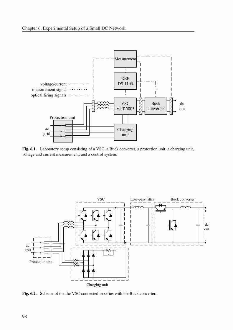
Chapter 6. Experimental Setup of a Small DC Network
VSCVLT 5003
dcout
acgrid
Protection unit
Buckconverter
Measurement
DSPDS 1103
Chargingunit
voltage/currentmeasurement signal
optical firing signals
Fig. 6.1. Laboratory setup consisting of a VSC, a Buck converter, a protection unit, a charging unit,voltage and current measurement, and a control system.
dcout
+
-ac
grid
Charging unit
Low-pass filter
Protection unit
Buck converterVSC
Fig. 6.2. Scheme of the the VSC connected in series with the Buck converter.
98
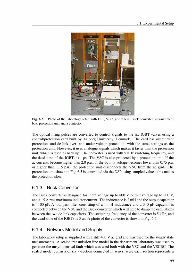
6.1. Experimental Setup
Fig. 6.3. Photo of the laboratory setup with DSP, VSC, grid filters, Buck converter, measurementbox, protection unit and a contactor.
The optical firing pulses are converted to control signals to the six IGBT valves using acontrol/protection card built by Aalborg University, Denmark. The card has overcurrentprotection, and dc-link-over- and under-voltage protection, with the same settings as theprotection unit. However, it uses analogue signals which makes it faster than the protectionunit, which is used as back up. The converter is used with 5 kHz switching frequency, andthe dead-time of the IGBTs is 1 µs. The VSC is also protected by a protection unit. If theac currents become higher than 2.0 p.u., or the dc-link voltage becomes lower than 0.75 p.u.or higher than 1.15 p.u. the protection unit disconnects the VSC from the ac grid. Theprotection unit shown in Fig. 6.5 is controlled via the DSP using sampled values; this makesthe protection slow.
6.1.3 Buck Converter
The Buck converter is designed for input voltage up to 800 V, output voltage up to 800 V,and a 15 A rms maximum inductor current. The inductance is 2 mH and the output capacitoris 1100 µF. A low-pass filter consisting of a 1 mH inductance and a 340 µF capacitor isconnected between the VSC and the Buck converter which will help to damp the oscillationsbetween the two dc-link capacitors. The switching frequency of the converter is 5 kHz, andthe dead-time of the IGBTs is 3 µs. A photo of the converter is shown in Fig. 6.6.
6.1.4 Network Model and Supply
The laboratory setup is supplied with a stiff 400 V ac grid and was used for the steady statemeasurements. A scaled transmission line model in the department laboratory was used togenerate the unsymmetrical fault which was used both with the VSC and the VSCBC. Thescaled model consists of six π-section connected in series, were each section represents a
99
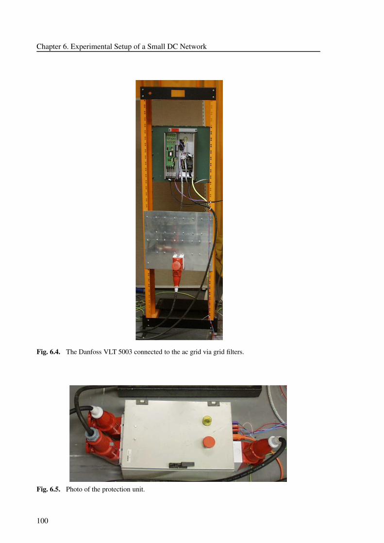
Chapter 6. Experimental Setup of a Small DC Network
Fig. 6.4. The Danfoss VLT 5003 connected to the ac grid via grid filters.
Fig. 6.5. Photo of the protection unit.
100
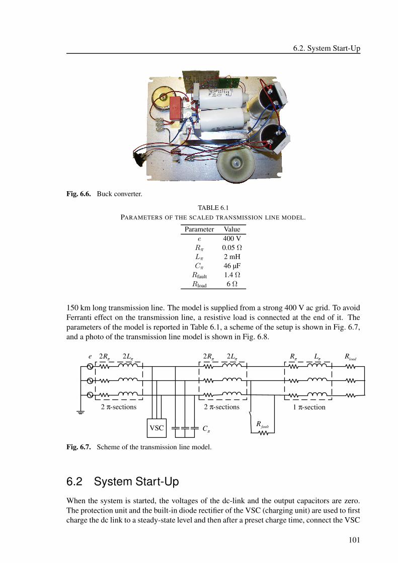
6.2. System Start-Up
Fig. 6.6. Buck converter.
TABLE 6.1PARAMETERS OF THE SCALED TRANSMISSION LINE MODEL.
Parameter Valuee 400 V
Rπ 0.05 ΩLπ 2 mHCπ 46 µF
Rfault 1.4 ΩRload 6 Ω
150 km long transmission line. The model is supplied from a strong 400 V ac grid. To avoidFerranti effect on the transmission line, a resistive load is connected at the end of it. Theparameters of the model is reported in Table 6.1, a scheme of the setup is shown in Fig. 6.7,and a photo of the transmission line model is shown in Fig. 6.8.
VSC
πR2 πL2 πL2 πLπR2 πR
πC faultR
loadRe
1 π-section2 π-sections2 π-sections
Fig. 6.7. Scheme of the transmission line model.
6.2 System Start-Up
When the system is started, the voltages of the dc-link and the output capacitors are zero.The protection unit and the built-in diode rectifier of the VSC (charging unit) are used to firstcharge the dc link to a steady-state level and then after a preset charge time, connect the VSC
101
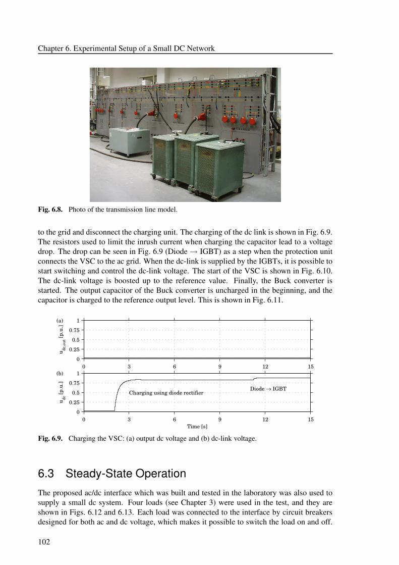
Chapter 6. Experimental Setup of a Small DC Network
Fig. 6.8. Photo of the transmission line model.
to the grid and disconnect the charging unit. The charging of the dc link is shown in Fig. 6.9.The resistors used to limit the inrush current when charging the capacitor lead to a voltagedrop. The drop can be seen in Fig. 6.9 (Diode → IGBT) as a step when the protection unitconnects the VSC to the ac grid. When the dc-link is supplied by the IGBTs, it is possible tostart switching and control the dc-link voltage. The start of the VSC is shown in Fig. 6.10.The dc-link voltage is boosted up to the reference value. Finally, the Buck converter isstarted. The output capacitor of the Buck converter is uncharged in the beginning, and thecapacitor is charged to the reference output level. This is shown in Fig. 6.11.
0 3 6 9 12 150
0.25
0.5
0.75
1
u dc,o
ut [p
.u.]
(a)
0 3 6 9 12 150
0.25
0.5
0.75
1
u dc [p
.u.]
(b)
Charging using diode rectifierDiode → IGBT
Time [s]
Fig. 6.9. Charging the VSC: (a) output dc voltage and (b) dc-link voltage.
6.3 Steady-State Operation
The proposed ac/dc interface which was built and tested in the laboratory was also used tosupply a small dc system. Four loads (see Chapter 3) were used in the test, and they areshown in Figs. 6.12 and 6.13. Each load was connected to the interface by circuit breakersdesigned for both ac and dc voltage, which makes it possible to switch the load on and off.
102
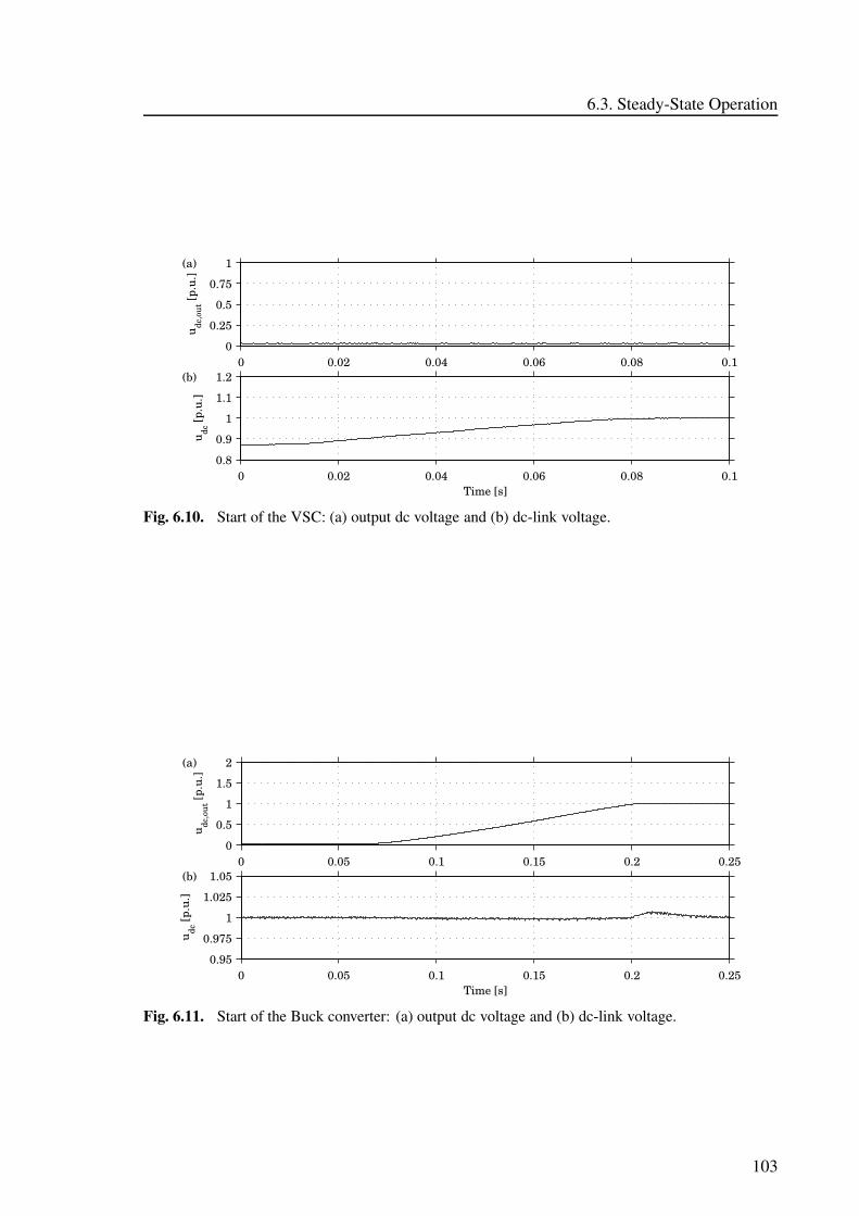
6.3. Steady-State Operation
0 0.02 0.04 0.06 0.08 0.10
0.25
0.5
0.75
1
u dc,o
ut [p
.u.]
(a)
0 0.02 0.04 0.06 0.08 0.10.8
0.9
1
1.1
1.2
u dc [p
.u.]
(b)
Time [s]
Fig. 6.10. Start of the VSC: (a) output dc voltage and (b) dc-link voltage.
0 0.05 0.1 0.15 0.2 0.250
0.5
1
1.5
2
u dc,o
ut [p
.u.]
(a)
0 0.05 0.1 0.15 0.2 0.250.95
0.975
1
1.025
1.05
u dc [p
.u.]
(b)
Time [s]
Fig. 6.11. Start of the Buck converter: (a) output dc voltage and (b) dc-link voltage.
103
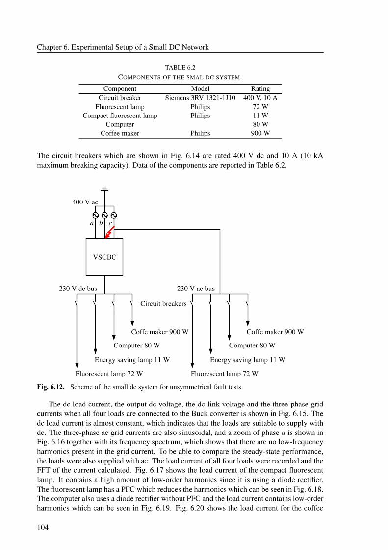
Chapter 6. Experimental Setup of a Small DC Network
TABLE 6.2COMPONENTS OF THE SMAL DC SYSTEM.
Component Model RatingCircuit breaker Siemens 3RV 1321-1J10 400 V, 10 A
Fluorescent lamp Philips 72 WCompact fluorescent lamp Philips 11 W
Computer 80 WCoffee maker Philips 900 W
The circuit breakers which are shown in Fig. 6.14 are rated 400 V dc and 10 A (10 kAmaximum breaking capacity). Data of the components are reported in Table 6.2.
VSCBC
230 V dc bus 230 V ac bus
Circuit breakers
400 V ac
Fluorescent lamp 72 W
Energy saving lamp 11 W
Computer 80 W
Coffe maker 900 W
Fluorescent lamp 72 W
Energy saving lamp 11 W
Computer 80 W
Coffe maker 900 W
a b c
Fig. 6.12. Scheme of the small dc system for unsymmetrical fault tests.
The dc load current, the output dc voltage, the dc-link voltage and the three-phase gridcurrents when all four loads are connected to the Buck converter is shown in Fig. 6.15. Thedc load current is almost constant, which indicates that the loads are suitable to supply withdc. The three-phase ac grid currents are also sinusoidal, and a zoom of phase a is shown inFig. 6.16 together with its frequency spectrum, which shows that there are no low-frequencyharmonics present in the grid current. To be able to compare the steady-state performance,the loads were also supplied with ac. The load current of all four loads were recorded and theFFT of the current calculated. Fig. 6.17 shows the load current of the compact fluorescentlamp. It contains a high amount of low-order harmonics since it is using a diode rectifier.The fluorescent lamp has a PFC which reduces the harmonics which can be seen in Fig. 6.18.The computer also uses a diode rectifier without PFC and the load current contains low-orderharmonics which can be seen in Fig. 6.19. Fig. 6.20 shows the load current for the coffee
104
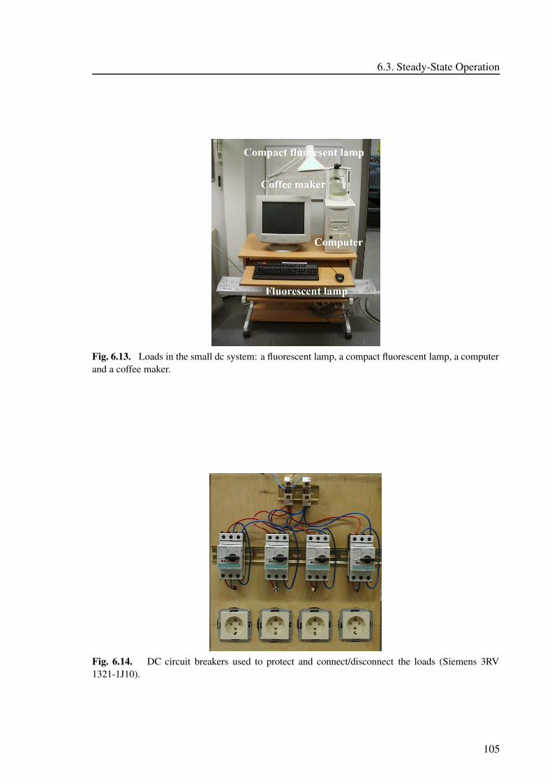
6.3. Steady-State Operation
Fig. 6.13. Loads in the small dc system: a fluorescent lamp, a compact fluorescent lamp, a computerand a coffee maker.
Fig. 6.14. DC circuit breakers used to protect and connect/disconnect the loads (Siemens 3RV1321-1J10).
105

Chapter 6. Experimental Setup of a Small DC Network
maker which is a purely resistive load, and therefore draws a purely sinusoidal grid current.The total load current is shown in Fig. 6.21. The load current is dominated by the coffeemaker, which reduces the content of harmonics in the grid current. Using only loads likethe computer would generate a high amount of harmonics. For supplying these loads, the dcsystem has the advantage of gaining balanced and harmonics free three-phase grid currents.
0 0.01 0.02 0.03 0.04 0.050.95
0.975
1
1.025
1.05
u dc,o
ut [p
.u.]
(a)
0 0.01 0.02 0.03 0.04 0.050.3
0.325
0.35
0.375
0.4
i load
[p.u
.]
(b)
0 0.01 0.02 0.03 0.04 0.050.95
0.975
1
1.025
1.05
u dc [p
.u.]
(c)
0 0.01 0.02 0.03 0.04 0.05−1
−0.5
0
0.5
1
i 1,i 2,i 3 [p.u
.]
(d)
Time [s]
Fig. 6.15. Operation of small dc network: (a) output dc voltage, (b) dc load current, (c) dc-linkvoltage and (d) three-phase grid currents.
0 0.005 0.001 0.0015 0.002 0.025−1
−0.5
0
0.5
1
i 1 [p.u
.]
(a)
Time [s]0 100 200 300 400 500 600
0
0.0025
0.005
0.0075
0.01
I N/I
1 [p.u
.]
(b)
Frequency [Hz]
Fig. 6.16. Phase current a of the VSC when all four loads are connected: (a) phase current and (b)FFT of the phase current.
106
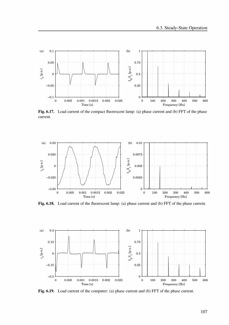
6.3. Steady-State Operation
0 0.005 0.001 0.0015 0.002 0.025−0.1
−0.05
0
0.05
0.1
i 3 [p.u
.]
(a)
Time [s]0 100 200 300 400 500 600
0
0.25
0.5
0.75
1
I N/I
1 [p.u
.]
(b)
Frequency [Hz]
Fig. 6.17. Load current of the compact fluorescent lamp: (a) phase current and (b) FFT of the phasecurrent.
0 0.005 0.001 0.0015 0.002 0.025−0.05
−0.025
0
0.025
0.05
i 3 [p.u
.]
(a)
Time [s]0 100 200 300 400 500 600
0
0.0025
0.005
0.0075
0.01
I N/I
1 [p.u
.]
(b)
Frequency [Hz]
Fig. 6.18. Load current of the fluorescent lamp: (a) phase current and (b) FFT of the phase current.
0 0.005 0.001 0.0015 0.002 0.025−0.3
−0.15
0
0.15
0.3
i 3 [p.u
.]
(a)
Time [s]0 100 200 300 400 500 600
0
0.25
0.5
0.75
1
I N/I
1 [p.u
.]
(b)
Frequency [Hz]
Fig. 6.19. Load current of the computer: (a) phase current and (b) FFT of the phase current.
107
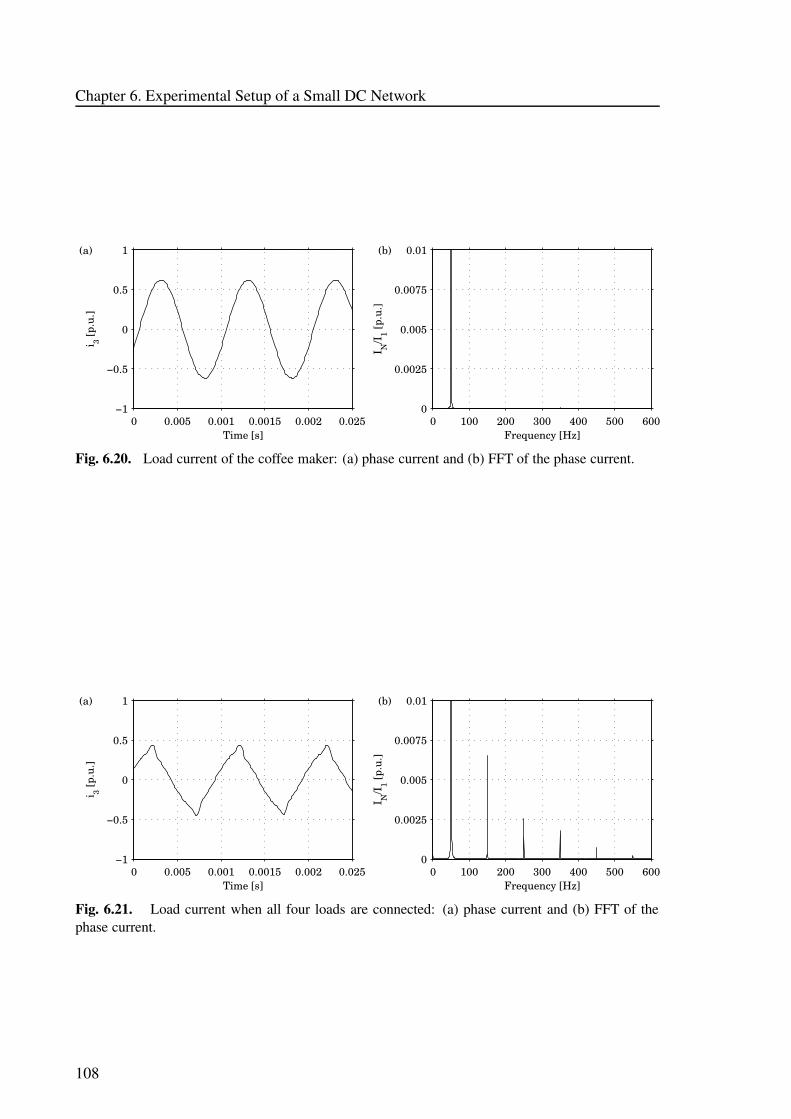
Chapter 6. Experimental Setup of a Small DC Network
0 0.005 0.001 0.0015 0.002 0.025−1
−0.5
0
0.5
1
i 3 [p.u
.]
(a)
Time [s]0 100 200 300 400 500 600
0
0.0025
0.005
0.0075
0.01
I N/I
1 [p.u
.]
(b)
Frequency [Hz]
Fig. 6.20. Load current of the coffee maker: (a) phase current and (b) FFT of the phase current.
0 0.005 0.001 0.0015 0.002 0.025−1
−0.5
0
0.5
1
i 3 [p.u
.]
(a)
Time [s]0 100 200 300 400 500 600
0
0.0025
0.005
0.0075
0.01
I N/I
1 [p.u
.]
(b)
Frequency [Hz]
Fig. 6.21. Load current when all four loads are connected: (a) phase current and (b) FFT of thephase current.
108
6.4. Transient Operation
6.4 Transient Operation
The system was studied during loads transients (connection and disconnection) and during adisturbance on the supplying ac grid.
6.4.1 Load Changes
The loads were connected in the following sequence: fluorescent lamp, compact fluorescentlamp, computer and finally the coffee maker. The idea was to reproduce a normal workingday in the office room. The loads are disconnected in the opposite order. Figs. 6.22, 6.23,6.24 and 6.25 show connection of the loads. The measurements show that the electronic loads(all loads except the coffee maker) have a large current transient when they are connected.The reason is that the loads have a capacitor which is charged when it is connected. Themeasurement using ac is shown in Fig. 6.26, which shows that the electronic loads also herehave a large current transient when it is connected.
Figs. 6.27, 6.28, 6.29 and 6.30 show disconnection of the loads. The measurement showsthat the electronic loads have a small current transient when they are disconnected. Thecoffee maker which is a large load causes a small voltage overshoot when it is disconnected.The measurement using ac shown in Fig. 6.31 show also that the loads have no currenttransients when they are disconnected.
0 0.01 0.02 0.03 0.04 0.050.97
0.98
0.99
1
1.01
u dc,o
ut [p
.u.]
(a)
0 0.01 0.02 0.03 0.04 0.050
0.20.40.60.8
1
i load
[p.u
.]
(b)
Time [s]
Fig. 6.22. Connection of fluorescent lamp: (a) output dc voltage and (b) dc load current.
6.4.2 Voltage Dips
The performance of the small dc network during a phase-to-phase fault [68] on the supplyingac grid is shown in Fig. 6.32. The measurement shows that during the dip the dc-link starts tooscillate due to the unbalance, but the output dc voltage is not affected, and the loads operateas normal during the fault. If the same load is supplied with single phase ac connected toone of the faulted phases as shown in Fig. 6.12; and making a new fault using the same faultimpedance the computer restarts and the fluorescent lamp is shut off. This can be seen fromthe current waveform, shown in Fig. 6.33(b), which changes 100 ms after the fault is applied.This is due to the computer which restarts. Since a dip occurs randomly the fault was notapplied at the same point on wave.
109
Chapter 6. Experimental Setup of a Small DC Network
0 0.01 0.02 0.03 0.04 0.050.97
0.98
0.99
1
1.01
u dc,o
ut [p
.u.]
(a)
0 0.01 0.02 0.03 0.04 0.050
0.10.20.30.40.5
i load
[p.u
.]
(b)
Time [s]
Fig. 6.23. Connection of compact fluorescent lamp: (a) output dc voltage and (b) dc load current.
0 0.01 0.02 0.03 0.04 0.050.9
0.95
1
1.05
1.1
u dc,o
ut [p
.u.]
(a)
0 0.01 0.02 0.03 0.04 0.050
0.5
1
1.5
2
i load
[p.u
.]
(b)
Time [s]
Fig. 6.24. Connection of computer: (a) output dc voltage and (b) dc load current.
0 0.01 0.02 0.03 0.04 0.050.97
0.98
0.99
1
1.01
u dc,o
ut [p
.u.]
(a)
0 0.01 0.02 0.03 0.04 0.050
0.1
0.2
0.3
0.4
i load
[p.u
.]
(b)
Time [s]
Fig. 6.25. Connection of coffee maker: (a) output dc voltage and (b) dc load current.
110
6.4. Transient Operation
0 0.01 0.02 0.03 0.04 0.05−0.3
0
0.3
0.6
0.9i 3 [p
.u.]
(a)
0 0.01 0.02 0.03 0.04 0.05−0.3
0
0.3
0.6
0.9
i 3 [p.u
.]
(b)
0 0.01 0.02 0.03 0.04 0.05−2
−1
0
1
2
i 3 [p.u
.]
(c)
0 0.01 0.02 0.03 0.04 0.05−1
−0.5
0
0.5
1
i 3 [p.u
.]
(d)
Time [s]
Fig. 6.26. Connection of loads using ac: (a) fluorescent lamp, (b) compact fluorescent lamp, (c)computer and (d) coffee maker.
0 0.01 0.02 0.03 0.04 0.050.98
0.99
1
1.01
1.02
u dc,o
ut [p
.u.]
(a)
0 0.01 0.02 0.03 0.04 0.050
0.1
0.2
0.3
0.4
i load
[p.u
.]
(b)
Time [s]
Fig. 6.27. Disconnection of coffee maker: (a) output dc voltage and (b) dc load current.
111
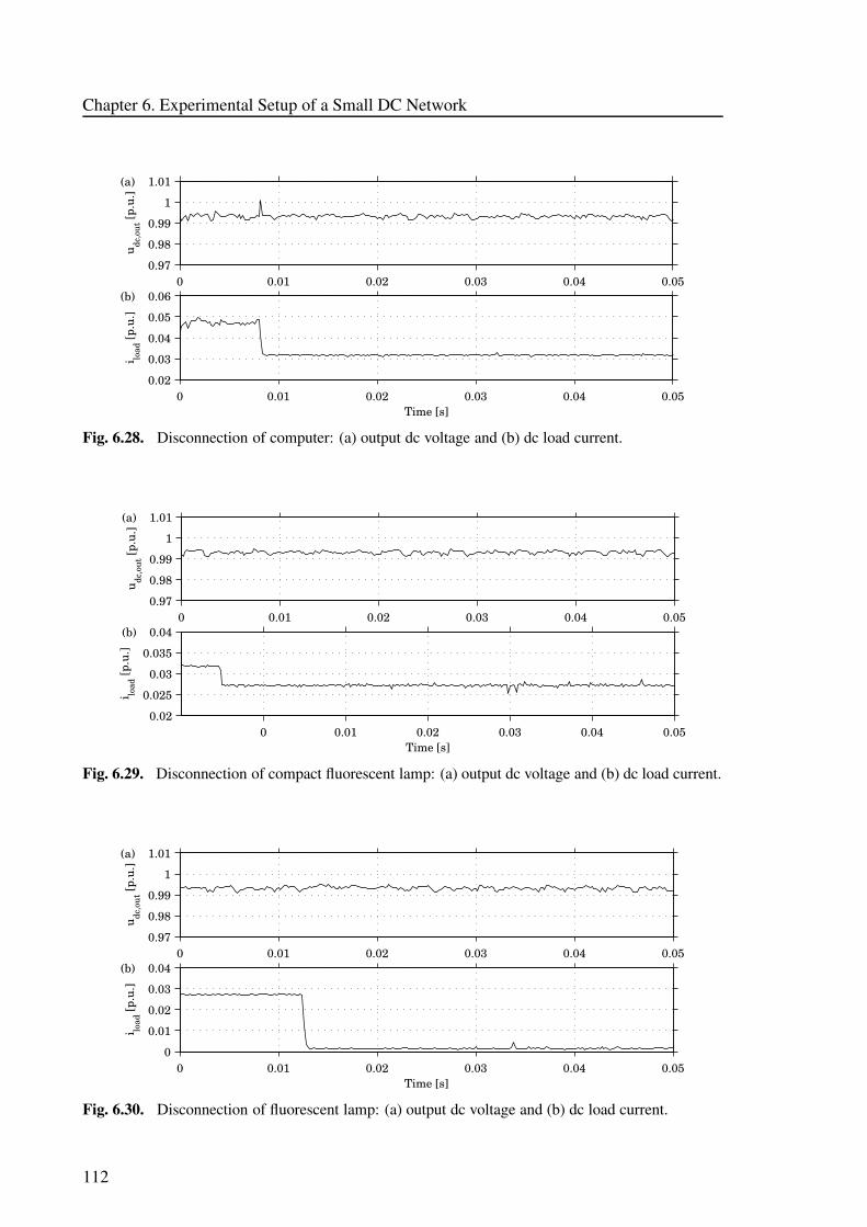
Chapter 6. Experimental Setup of a Small DC Network
0 0.01 0.02 0.03 0.04 0.050.97
0.98
0.99
1
1.01
u dc,o
ut [p
.u.]
(a)
0 0.01 0.02 0.03 0.04 0.050.02
0.03
0.04
0.05
0.06
i load
[p.u
.]
(b)
Time [s]
Fig. 6.28. Disconnection of computer: (a) output dc voltage and (b) dc load current.
0 0.01 0.02 0.03 0.04 0.050.97
0.98
0.99
1
1.01
u dc,o
ut [p
.u.]
(a)
0 0.01 0.02 0.03 0.04 0.050.02
0.025
0.03
0.035
0.04
i load
[p.u
.]
(b)
Time [s]
Fig. 6.29. Disconnection of compact fluorescent lamp: (a) output dc voltage and (b) dc load current.
0 0.01 0.02 0.03 0.04 0.050.97
0.98
0.99
1
1.01
u dc,o
ut [p
.u.]
(a)
0 0.01 0.02 0.03 0.04 0.050
0.01
0.02
0.03
0.04
i load
[p.u
.]
(b)
Time [s]
Fig. 6.30. Disconnection of fluorescent lamp: (a) output dc voltage and (b) dc load current.
112
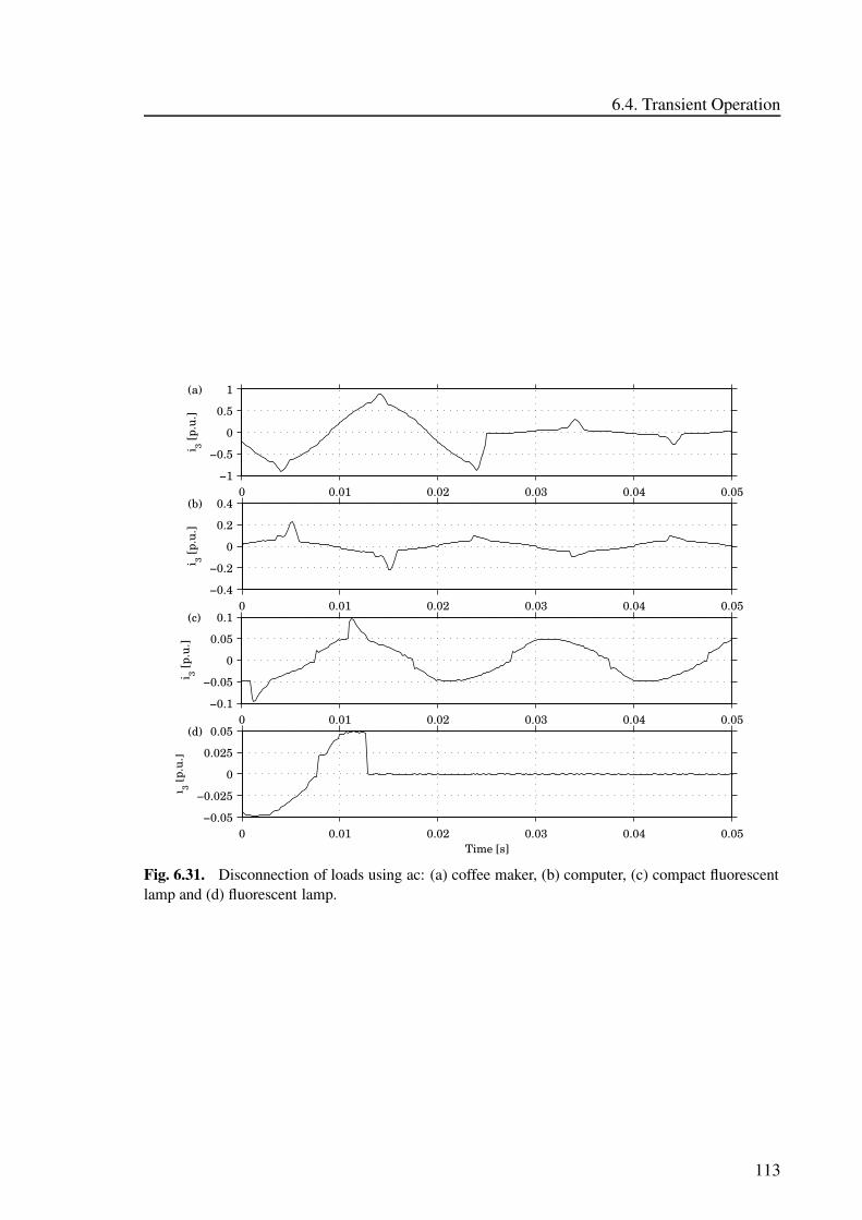
6.4. Transient Operation
0 0.01 0.02 0.03 0.04 0.05−1
−0.5
0
0.5
1
i 3 [p.u
.]
(a)
0 0.01 0.02 0.03 0.04 0.05−0.4
−0.2
0
0.2
0.4
i 3 [p.u
.]
(b)
0 0.01 0.02 0.03 0.04 0.05−0.1
−0.05
0
0.05
0.1
i 3 [p.u
.]
(c)
0 0.01 0.02 0.03 0.04 0.05−0.05
−0.025
0
0.025
0.05
i 3 [p.u
.]
(d)
Time [s]
Fig. 6.31. Disconnection of loads using ac: (a) coffee maker, (b) computer, (c) compact fluorescentlamp and (d) fluorescent lamp.
113
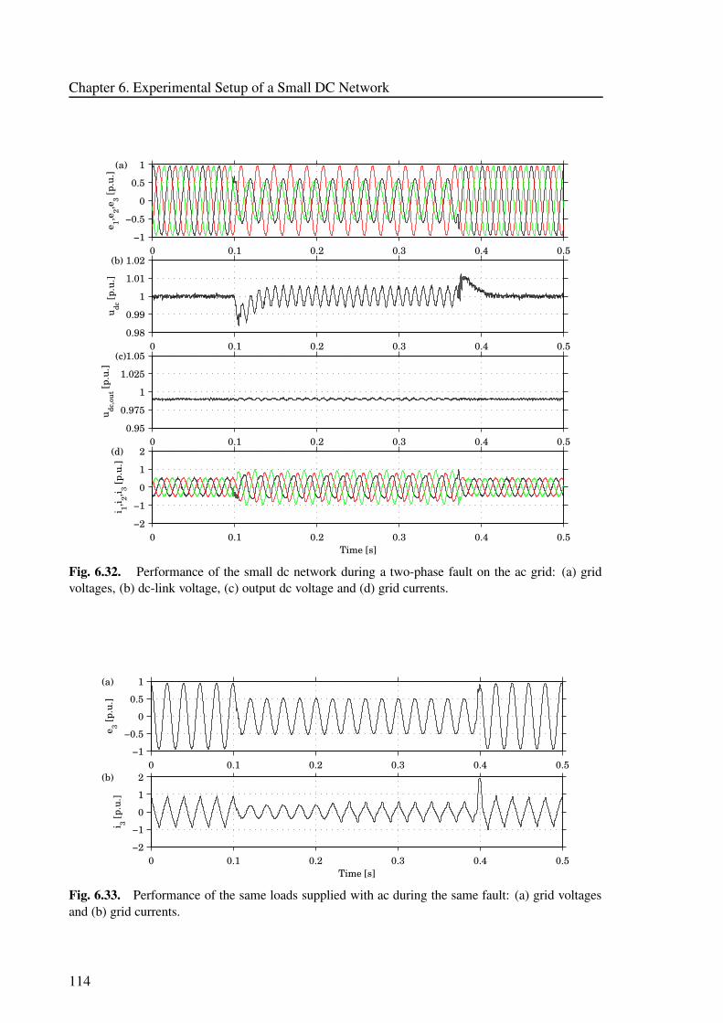
Chapter 6. Experimental Setup of a Small DC Network
0 0.1 0.2 0.3 0.4 0.5−1
−0.5
0
0.5
1
e 1,e2,e
3 [p.u
.]
(a)
0 0.1 0.2 0.3 0.4 0.50.98
0.99
1
1.01
1.02
u dc [p
.u.]
(b)
0 0.1 0.2 0.3 0.4 0.50.95
0.975
1
1.025
1.05
u dc,o
ut [p
.u.]
(c)
0 0.1 0.2 0.3 0.4 0.5−2
−1
0
1
2
i 1,i 2,i 3 [p.u
.]
(d)
Time [s]
Fig. 6.32. Performance of the small dc network during a two-phase fault on the ac grid: (a) gridvoltages, (b) dc-link voltage, (c) output dc voltage and (d) grid currents.
0 0.1 0.2 0.3 0.4 0.5−1
−0.5
0
0.5
1
e 3 [p.u
.]
(a)
0 0.1 0.2 0.3 0.4 0.5−2
−1
0
1
2
i 3 [p.u
.]
(b)
Time [s]
Fig. 6.33. Performance of the same loads supplied with ac during the same fault: (a) grid voltagesand (b) grid currents.
114
6.5. Conclusions
6.5 Conclusions
In this chapter, a laboratory system built to test the developed ac/dc interface is described.This system was used to obtain all measurements presented in Chapter 4 and 5, and also tosupply a small dc system with four loads. The system was compared with an identical systemsupplied with ac both during steady state and ac faults. The steady-state measurements showthat the interface produces sinusoidal grid currents without low-order harmonics and theloads, when supplied with ac, produce low-order harmonics. Using the interface improvesthe power quality by removing low-order harmonics and balancing the three phase currents.The comparison during an ac disturbance is not quite fair in the sense that the ac loads aresupplied by a single phase and the dc system with three phases. Practical limitations in thelaboratory when making faults also made it difficult to show how the design and controlimproves the sensitivity of the interface more than that “adding capacitors will save thesystem”.
115

Chapter 7
Conclusions and Future Work
7.1 Conclusions
In this thesis, the use of dc in low-voltage systems has been studied. Chapter 2 presented anoverview of existing dc systems and a brief survey of loads, generation and components foruse in dc systems clearly indicating that a low-voltage dc distribution system has a potentialto be used in future power systems.
Load modeling for transient and steady-state analysis of low-voltage dc systems was thesubject of Chapter 3. One important conclusion from the measurement series carried out oncommon household appliances is that most loads are able to operate with dc supply in a widevoltage range without any modifications. These can be classified into three main categories:resistive loads; electronic loads; and rotating loads. Exceptions are loads with inductive partsand some rotating loads, which cannot operate without an alternating supply. Resistive loadscould be further divided into heaters, which are modeled by a constant resistance both insteady state and during transients, and lighting appliances, which are modelled as a currentdependent resistor with a time constant that models the transient behavior. For rotatingloads, the steady-state model was found to be a voltage dependent current source, whereasthe transient behavior could only be reproduced using a mathematical expression. Electronicloads were further divided into power supplies, modeled as a constant power load combinedwith an RLC-circuit behind a diode rectifier, and lighting appliances, modeled as a constantcurrent load or a constant power load (depending on the control of the ballast), also combinedwith an RLC-circuit behind a diode rectifier.
To provide a high-quality interface between the ac and dc systems, a Voltage Source Con-verter (VSC) in series with a Buck converter was chosen for this project. Chapter 4 describedthe control of the VSC. This is a combination of current control, to keep the ac currents sinu-soidal and balanced, and dc-link voltage control, which provides the active current referenceto the current control in order to keep the dc voltage constant in case of load changes andac system disturbances. Three different dc-link voltage controllers were implemented andtested both in simulations and through experiments on a small laboratory system. The ef-fect of different capacitor sizes, bandwidths of the controllers and load types was studied.Among the three, the energy-balance dc-link-voltage controller (EB) showed the slowestresponse, but is free from oscillations due to its first order characteristic. The load-current-feed-forward dc-link-voltage controller (LC), which measures the dc load current, shows afaster response but with oscillations of the dc-link voltage. In the observer-load-current-feed-forward dc-link-voltage controller (OLC), a variant of the LC where the dc load current
117
Chapter 7. Conclusions and Future Work
is calculated by an observer, the calculation time taken by the observer makes the responseslower with respect to LC, but still faster than EB. The main conclusion is that LC is thebest choice if the dc load current can be measured. Otherwise EB should be used if therequirements on maximum allowed dc-voltage ripple are particularly tight.
However, when the VSC is connected in series to a Buck converter, which also is con-trolled by PWM in order to keep a stable output dc voltage, the differences among the threecontrollers are of less importance. As shown in Chapter 5, EB shows the best performancein this case, since it is not affected by the distorted dc load current generated by the Buckconverter. It is important here to remark that the proposed interface fulfills the requirementsspecified for this project, ensuring sinusoidal ac grid currents and good performance duringload step changes and faults and disturbances on the ac system. However, this topology isexpected to be quite costly and to have high losses, at least with the components available to-day. Nevertheless, it is particularly suited for a laboratory setup, since it gives a controllabledc-link voltage that can be varied in a wide range.
Chapter 6 presented in detail the laboratory system built to test the ac/dc interface de-veloped. The interface, rated 3 kVA, was used to supply a small dc system with four loads,representing a typical office. The system was compared with an identical system suppliedwith ac both during steady state and ac grid faults. The steady-state measurements show thatthe dc system with the proposed interface improves the power quality by balancing the threeac phase currents and removing low-order harmonics, otherwise present in the current whenthe loads are supplied with ac. It can be argued that the comparison during an ac disturbanceis quite not fair in the sense that the ac loads are supplied by a single phase and the dc systemwith three phases, which are not all faulted. Practical limitations when applying faults in thelaboratory made it difficult to show how the design and control improves the sensitivity ofthe interface.
Despite these limitations, the small laboratory test setup built within this project provedthat a dc system for low-voltage installations is fully feasible and can be preferred to a con-ventional, 50-Hz ac system in applications where many electronic loads are used, high re-liability and power quality are desired, and/or low magnetic fields are required. Besidescommon office buildings, these might be for example web hotels, data centers, banks, tele-com stations, hospitals, and military applications.
7.2 Future Work
Remaining Issues: System Optimization, Protection and Grounding
An item of interest for future work is the study of a larger dc system including energy storageand generation. A question is how to control the system during different operation modes.During periods of high generation and low consumption, the surplus power can be eitherstored in the energy storage or injected into the ac system. This problem can be extendedto include an economical aspect. When is it better to sell the power than to store it? Thiswill depend also on the speed of response of different generating sources and energy storagetechnologies to dynamic changes. Other questions are what would be the most suitableenergy storage technology for such applications and how should the optimal size of energystorage be chosen? With the proposed interface between ac and dc system, the short circuitpower of the dc system is limited to the energy in the dc-link capacitance. This will not
118
7.2. Future Work
be enough to use fuses for interrupting short circuit currents due to faults in the dc system.Moreover, fault detection becomes difficult. What other types of devices can be used todisconnect a fault, and how is the fault detected? Protection issues, along with personellsafety and grounding, are important questions to answer before a dc distribution system canbe applied in practice. For practical applications, a more strictly cost-driven design of theac/dc interface should also be carried out.
DC Microgrid Systems
Recently, in conjunction with several blackouts and supply interruptions due to human er-ror, poor maintenance, and extreme weather events [71], the concept of local small gridsequipped with some form of local generation and/or storage, called “microgrids” [72], hasbeen gaining increasing attention. A microgrid should be able to operate both connectedto a larger grid and in “island” operation, and be able to switch between the two operatingmodes without any impact on the operation of the local loads [73]. A dc-based microgridcan be an option to combine high reliability and low magnetic fields with high controlla-bility and a simpler system, due to simpler connection of generators and energy storage.A challenge is how to design such system optimizing supply availability vs. cost, particu-larly if the generation used is renewable-based, using intermittent sources such as wind orsun. Charge/discharge cycles of the energy storage devices should be considered, possiblyin combination with load management systems. Other interesting questions are how to de-tect the conditions for disconnection/reconnection of the dc island and how to perform thesequence of operations leading from grid-connected to island operation and vice versa.
Multilevel DC Systems and Other Applications
On a longer time scale, a future dc distribution system might include more than one voltagelevel, where dc could be used for high or medium voltage distribution in a part of a town,down to dc/dc-converter stations, replacing traditional transformer stations. There, the dcvoltage is stepped down to low voltage, which is used to transmit the power locally, i.e. tobuildings and offices. One could even go one step further and imagine a central, high powerdc-dc converter station receiving power through a HVDC link, and stepping it down to amedium voltage dc network.
Another area for possible dc applications is industrial systems [74]. Rolling mills orpaper mills today are completely automated and use drive systems. By using dc, all rectify-ing stages can be removed and the motors with their inverters can be coupled to the dc bus.Normally, much more freedom is allowed in the design of industrial systems, as opposedto utility systems, which results in a higher level of acceptance of new ideas. Moreover, anumber of new factories are being built today in emerging economies in East Asia, whichmakes it possible to adopt a new concept for the design if it can be shown to have major ad-vantages. The power level is much higher than what has been considered in this project, so afeasibility study should be made to determine the most suitable voltage level, and the avail-ability of necessary switching and protection devices for this application. Due to obvioussimilarities with an industrial system, an offshore wind park is another possible applicationof low- or medium-voltage dc system [75], particularly if using wind turbines with full-sizepower-electronic conversion.
119

References
[1] J. Benner and L. Kazmerski, “Photovoltaics gaining greater visibility,” IEEE Spectr.,vol. 36, no. 9, pp. 34–42, Sept. 1999.
[2] R. Wolk, “Fuel cells for home and hospitals,” IEEE Spectr., vol. 36, no. 5, pp. 45–52,May 1999.
[3] Short-circuit currents in dc auxiliary installations in power plants and substations, IEC61660, 1997.
[4] IEEE Recommended practice for the design of dc auxiliary power systems for generat-ing stations, IEEE Std. 946, 1992.
[5] C. Sulzberger, “Triumph of ac - from Pearl Street to Niagara,” IEEE Power EnergyMag., vol. 1, no. 3, pp. 64–67, May/June 2003.
[6] ——, “Triumph of ac - the battle of the currents,” IEEE Power Energy Mag., vol. 1,no. 4, pp. 70–73, July/Aug. 2003.
[7] G. Woodward, “History of a single-phase high-voltage distribution system,” Proc.IEEE, vol. 140, no. 3, pp. 207–214, May 1993.
[8] T. Gruzs, “Powering telecom and info technology systems,” Power Quality Assurance,pp. 22–29, Apr. 2001.
[9] K. Mizuguchi, S. Muroyama, Y. Kuwata, and Y. Ohashi, “A new decentralized dc powersystem for telecommunications systems,” in Proc. IEEE INTELEC’90, Orlando, FL,Oct. 21–25 1990, pp. 55–62.
[10] T. Yamashita, S. Muroyama, S. Furubo, and S. Ohtsu, “270 V dc system - a highlyefficient and reliable power supply system for both telecom and datacom systems,” inProc. IEEE INTELEC’99, Copenhagen, Denmark, June 6–9 1999.
[11] T. Gruzs and J. Hall, “AC, dc or hybrid power solutions for today’s telecommunicationsfacilities,” in Proc. IEEE INTELEC’00, Phoenix, AZ, Sept. 2000, pp. 361–368.
[12] C. Chan, “An overview of electric vehicle technology,” Proc. IEEE, vol. 81, no. 9, p.1202, 1993.
[13] A. Emadi, M. Ehsani, and J. Miller, Vehicular electric power systems, 1st ed. NewYork, NY: Marcel Dekker, 2004.
121
REFERENCES
[14] C. Chan, “The state of the art of electric and hybrid vehicles,” Proc. IEEE, vol. 90,no. 2, pp. 247–275, Feb. 2002.
[15] J. Miller, “Power electronics in hybrid electric vehicle applications,” in Proc. IEEEAPEC’03, vol. 1, Miami Beach, FL, Feb. 9–13 2003, pp. 23–29.
[16] “Technology for Future Naval Forces,” [online] Available:http://www.nap.edu/html/tech 21st/ (last accessed on 2005-05-09).
[17] M. Baran and N. Mahajan, “DC distribution for industrial systems: opportunities andchallenges,” IEEE Trans. Ind. Applicat., vol. 39, no. 6, pp. 1596–1601, Nov./Dec. 2003.
[18] T. Doyle, H. Stevens, and H. Robey, “An historical overview of navy electricdrive,” [online] Available: www.onr.navy.mil/fncs/aces/docs/history.pdf (last accessedon 2005-03-07).
[19] J. Momoh, S. Kaddah, and W. Salawu, “Security assessment of dc zonal naval-shippower system,” in Large Engineering Systems Conference on Power Engineering (LE-SCOPE’01), Halifax, NS, Canada, July 11–13 2001, pp. 206–212.
[20] T. McCoy, “Trends in ship electric propulsion,” in Proc. IEEE Power Engineering Soc.Summer Meeting, vol. 1, Chicago, IL, July 21–25 2002, pp. 343–346.
[21] D. Paul, “DC traction power system grounding,” IEEE Trans. Ind. Applicat., vol. 38,no. 3, pp. 818–824, May/June 2002.
[22] R. Hill, “Electric railway traction. Part 3. Traction power supplies,” Power EngineeringJournal, vol. 8, pp. 275–286, Dec. 1994.
[23] N. Hingorani, “High-voltage dc transmission: a power electronics workhorse,” IEEESpectr., vol. 33, no. 4, pp. 63–72, Apr. 1996.
[24] D. Andersson and A. Henriksson, “Passive and active dc breakers in the Three Gorges-Changzhou HVDC project,” in Proc. IPCS02, Wuhan, Hubei, China, Sept. 3–5 2002.
[25] G. Asplund, K. Eriksson, and K. Svensson, “DC transmission based on voltage sourceconverters,” in CIGRE Conf., no. 14-302, Paris, France, 1998.
[26] Y. Ito, Z. Yang, and H. Akagi, “DC micro-grid based distribution power generationsystem,” in Proc. International Power Electronics and Motion Control Conference(IPEMC’04), vol. 3, Aug. 14–16 2004, pp. 1740–1745.
[27] EMC levels in low voltage distribution systems (in Swedish), SS 4211811, 1989.
[28] Voltage characteristics of electricity supplied by public distribution systems, EN50160:2000, 2000.
[29] IEEE Recommended pratice and requirements for harmonics control in electric powersystems, IEEE Std. 519-1992, 1992.
[30] J. Enslin, “Interconnection of distributed power to the distribution system,” in Proc.IEEE PSCE’04, New York, NY, Oct. 10–13 2004, pp. 1718–1723.
122
REFERENCES
[31] A. Agustoni, E. Borioli, P. Ferrari, A. Mariscotti, E. Picco, P. Pinceti, and G. Simioli,“LV dc networks for distributed energy resources,” in Proc. Cigre Symposium on PowerSystem with Dispersed Generation, Athens, Greece, Apr. 13–16 2005.
[32] J. Ferreira and H. van der Broeck, “Alternative power distribution in residential andcommercial buildings,” in Proc. of Fifth European Conference on Power Electronicsand Applications (EPE’93), vol. 7, Brighton, UK, Sept. 13–16 1993, pp. 188–193.
[33] L. Po-Wa, L. Yim-Zhu, and L. Bo-Tao, “Power distribution systems for future homes,”in Proc. IEEE PEDS’99, vol. 2, Hong Kong, July 27–29 1999, pp. 1140–1146.
[34] A. Sannino, G. Postiglione, and M. Bollen, “Feasibility of a dc network for commercialfacilities,” IEEE Trans. Ind. Applicat., vol. 39, no. 5, pp. 1499–1507, Sept./Oct. 2003.
[35] Elforsk, Ericsson, SEK, Stockholm Energi, Telia, Sydkraft och Vattenfall, “Likstromfor drift av elektrisk utrustning i fastigheter - Forstudie,” ELFORSK, Sweden, Tech.Rep. 99:3 (in Swedish), 1999.
[36] J.-E. Alm, “Alternativt spanningssystem i bostader, Tech. Rep. (in Swedish), 1998.
[37] J. Pellis, “The dc low-voltage house,” Master’s thesis, Eindhoven University of Tech-nology, The Netherlands, Sept. 1997.
[38] Power cables of rated voltage 0,6/1 kV - Specifications for design and testing (inSwedish), SS 4241418, 2003.
[39] Power system protection - principles and components, 2nd ed. P. Peregrinus Ltd.,Stevenage, UK and New York, 1990, vol. 1.
[40] 3RV1 Circuit Breaker/MSP, [online] Available: http://cache.automation.siemens.com/dnl/TY1Nzg1NwAA 6009084 HB/02sirius en.pdf (last accessed on 2005-05-09).
[41] G. Gregory, “Applying low-voltage circuit breakers in direct current systems,” IEEETrans. Ind. Applicat., vol. 31, no. 4, pp. 650–657, July/Aug. 1995.
[42] C. Kimblin and R. William, “Low-voltage power circuit breakers and molded case cir-cuit breakers-a comparison of test requirements,” in Proc. IEEE Industrial and Com-mercial Power Systems Technical Conference, Pitsburgh, PA, May 2–6 1999.
[43] Eaton Arc Twister HVDC Contactors, Sarasota, FL.
[44] P. McEwan and S. Tennakoon, “A two-stage dc thyristor circuit breaker,” IEEE Trans.Power Electron., vol. 12, no. 4, pp. 597–607, July 1997.
[45] R. Erickson and D. Maksimovic, Fundamentals of power electronics. Kluwer Aca-demic Publishers, Norwell, MA, 2002.
[46] W. R. N. Mohan, T. Undeland, Power electronics converter, applications, and design,2nd ed. New York, NY: John Wiley & Sons, Inc., 1996.
123
REFERENCES
[47] K. D. Gusseme, D. V. de Sype, and J. Melkebeek, “Design issues for digital control ofboost power factor correction converters,” in Proc. IEEE International Symposium onIndustrial Electronics (ISIE’02), vol. 3, Ghent, Belgium, May 26–29 2002, pp. 731–736.
[48] M. Lindgren, “Modeling and control of voltage source converters connected to thegrid,” Ph.D. dissertation, Chalmers University of Technology, Gothenburg, Sweden,1998.
[49] J. Svensson, “Grid-connected voltage source converters,” Ph.D. dissertation, ChalmersUniversity of Technology, Gothenburg, Sweden, 1998.
[50] L. Hongtao, X. Zheng, and G. Zhi, “A control strategy for three-level VSC-HVDCsystem,” in Proc. IEEE Power Engineering Soc. Summer Meeting, vol. 1, Chicago, IL,July 21–25 2002, pp. 480–485.
[51] E. Einarsson and B.-O. Wickbom, “Load modelling for steady-state and transient anal-ysis of low-voltage dc systems,” Master’s thesis, Chalmers Universisty of Technology,Gothenburg, Sweden, 2004.
[52] D. Nilsson and A. Sannino, “Load modelling for steady-state and transient analysis oflow-voltage dc systems,” in Conf. Rec. IEEE-IAS Annu. Meeting, vol. 2, Seattle, WA,Oct. 3–8 2003, pp. 774–780.
[53] IEEE Recommended practice for industrial and commercial power system analysis,IEEE Std. 399, 1997.
[54] K. Linden and I. Segerqvist, “Modelling of load devices and studying load/systemcharacteristics,” Chalmers University of Technology, Gothenburg, Sweden, Tech. Rep.131L, 1992.
[55] P. Cen, Principles of electric machines and power electronics, 2nd ed. New York, NY:John Wiley & Sons, Inc., 1996.
[56] H. Cheng, C. Moo, H. Yen, T. Lin, and S. Huang, “Single-switch high-power-factorelectronic ballast for compact fluorescent lamps,” in Proc. IEEE PEDS’01, vol. 2, In-donesia, Oct. 22–25 2001, pp. 764–769.
[57] Y.-C. Wu, T.-F. Wu, and Y.-K. Chen, “A compact single-stage converter for emergencylighting applications,” in Proc. IEEE PESC’02, vol. 2, Cairns, Australia, June 23–272002, pp. 779–784.
[58] S. Lee, H.-H. Chung, and S. Hui, “A novel electrode power profiler for dimmable bal-lasts using dc link voltage and switching frequency controls,” IEEE Trans. Power Elec-tron., vol. 19, no. 3, pp. 847–853, May 2004.
[59] M. Kazmierkowski, R. Krishnan, and F. Blaabjerg, Control in power electronics - se-lected problems. Academic press, San Diego, CA, 2002.
[60] L. Harnefors, Control of variable-speed drives. Vasteras, Sweden: Applied SignalProcessing and Control, Dept. of Electronics, Malardalen University, 2002.
124
REFERENCES
[61] N. Hingorani and L. Gyugyi, Understanding FACTS. Piscataway, NJ: IEEE Press,2000.
[62] M. Alakula, Power electronics control. Lund University, Sweden, 2002.
[63] S. Bowes and P. Clark, “Regular-sampled harmonic-elimination PWM control of in-verter drives,” in IEEE Trans. Power Electron., vol. 10, no. 5, Sept. 1995, pp. 521–531.
[64] M. Bongiorno, “Control of voltage source converters for voltage dip mitigation in shuntand series configurations,” Chalmers University of Technology, Gothenburg, Sweden,Tech. Rep. 515L, 2004.
[65] R. Ottersten and J. Svensson, “Vector current controlled voltage source converter -deadbeat control and saturation strategies,” IEEE Trans. Power Electron., vol. 17, no. 2,pp. 279–285, Mar. 2002.
[66] R. Ottersten, “On control of back-to-back converters and sensorless induction machinedrives,” Ph.D. dissertation, Chalmers University of Technology, Gothenburg, 2003.
[67] Z. Zhou, Y. Liu, and P. Unsworth, “Design of dc link current observer for a 3-phase ac-tive rectifier with feedforward control,” in Conf. Rec. IEEE-IAS Annu. Meeting, vol. 1,Seattle, WA, Oct. 3–7 2004, pp. 468–475.
[68] M. Bollen, Understanding power quality. Piscataway, NJ: IEEE Press, 2000.
[69] dSPACE, Solutions for Control, [online] Available:http://www.dspace.de/ww/en/pub/home.htm (last accessed on 2005-05-10).
[70] Danfoss design guide for frequency converters VLT 5000, [online] Available:http://www.danfoss.com (last accessed on 2005-05-10).
[71] Ny Teknik “Gudruns harjningar kostar en halv miljard” (in Swedish), [online] Avail-able: http://www.nyteknik.se/pub/ipsart.asp?art id=38287 (last accessed on 2005-05-11).
[72] R. Lasseter and P.Paigi, “Microgrid: a conceptual solution,” in Proc. IEEE PESC’04,vol. 6, Aachen, Germany, June 20–25 2004, pp. 4285–4290.
[73] R. Lasseter, “Microgrids,” in Proc. IEEE Power Engineering Soc. Winter Meeting,vol. 1, New York, NY, Jan. 27–31 2002, pp. 305–308.
[74] C. Du, “The control of VSC-HVDC and its use for large industrial power systems,”Chalmers University of Technology, Gothenburg, Sweden, Tech. Rep. 484L, 2003.
[75] S. Lundberg, “Configuration study of large wind parks,” Chalmers University of Tech-nology, Gothenburg, Sweden, Tech. Rep. 474L, 2003.
125