data sheet: technical data - nxp semiconductors · data sheet: technical data freescale reserves...
TRANSCRIPT

© Freescale Semiconductor, Inc., 2005–2011. All rights reserved.
Freescale SemiconductorData Sheet: Technical Data
Freescale reserves the right to change the detail specifications as may be required to permit improvements in the design of itsproducts.
Document Number: MBC13720Rev. 4, 09/2011
MBC13720
Package InformationPlastic Package
Case 419B(SOT-363)
Ordering Information
DeviceDevice Marking or
Operating Temperature Range
Package
MBC13720NT11
1 Refer to Table 1.
20N SOT-363
1 IntroductionThe MBC13720 is a high IP3, low noise amplifier designed for 400 MHz to 2.4 GHz multi-standard wireless applications. The input and output match is external to allow maximum design flexibility. The LNA has two selectable current settings as well as a standby mode. The LNA operates from a 2.5 to 3.0 V supply. The MBC13720 is fabricated using an advanced RF BiCMOS process with the SiGe:C option and is housed in an ultra small SOT-363 surface mount package.
1.1 Features• Selectable current, 5.0 mA or 11 mA
• Standby mode to turn off device completely
• High Input IP3:10 dBm @ 1.9 GHz13 dBm @ 2.4 GHz
• Low Noise Figure:1.38 dB @ 1.9 GHz1.55 dB @ 2.4 GHz
MBC13720SiGe:C Low Noise Amplifier with Bypass Switch
Contents1 Introduction . . . . . . . . . . . . . . . . . . . . . . . . . . 12 Ordering Information . . . . . . . . . . . . . . . . . . . 23 Electrical Specifications . . . . . . . . . . . . . . . . 34 Parameters . . . . . . . . . . . . . . . . . . . . . . . . . . . 55 Application Information . . . . . . . . . . . . . . . . . 96 Packaging . . . . . . . . . . . . . . . . . . . . . . . . . . . 157 Product Documentation . . . . . . . . . . . . . . . . 15

Ordering Information
MBC13720 Technical Data, Rev. 4
2 Freescale Semiconductor
• Gain @ 9.0 mA, 2.75 V:14.5 dB @ 1.9 GHz12 dB @ 2.4 GHz
• Suitable for use from 400 MHz to 2.4 GHz
• Bias stabilized for device and temperature variations
• Ultra small SOT-363 surface mount package
• Available only in tape and reel packaging
• Available only in a lead free version (device number MBC13720NT1) (Refer to Table 1.)
Figure 1. Pin Connections
2 Ordering InformationTable 1 provides additional details on MBC13720 orderable parts.
Table 1. Orderable Parts Details
Device Operating Temp
Range (TA.)Package Lead Frame
RoHS Compliant
PB-FreeMSL Level
Solder Temp
MBC13720NT1 -40° to 85° C Tape and Reel Pb Free Yes Yes 1 260° C
2
1
34
5
6Bias
Control
RF IN RF OUT
BIAS
ENABLE 2ENABLE 1
GND
Electrical Specifications
MBC13720 Technical Data, Rev. 4
Freescale Semiconductor 3
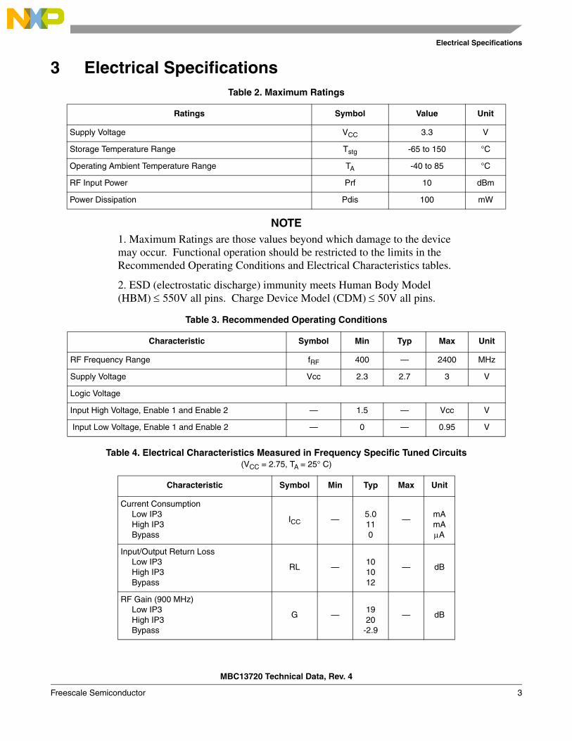
3 Electrical Specifications
NOTE1. Maximum Ratings are those values beyond which damage to the device may occur. Functional operation should be restricted to the limits in the Recommended Operating Conditions and Electrical Characteristics tables.
2. ESD (electrostatic discharge) immunity meets Human Body Model (HBM) ≤ 550V all pins. Charge Device Model (CDM) ≤ 50V all pins.
Table 2. Maximum Ratings
Ratings Symbol Value Unit
Supply Voltage VCC 3.3 V
Storage Temperature Range Tstg -65 to 150 °C
Operating Ambient Temperature Range TA -40 to 85 °C
RF Input Power Prf 10 dBm
Power Dissipation Pdis 100 mW
Table 3. Recommended Operating Conditions
Characteristic Symbol Min Typ Max Unit
RF Frequency Range fRF 400 — 2400 MHz
Supply Voltage Vcc 2.3 2.7 3 V
Logic Voltage
Input High Voltage, Enable 1 and Enable 2 — 1.5 — Vcc V
Input Low Voltage, Enable 1 and Enable 2 — 0 — 0.95 V
Table 4. Electrical Characteristics Measured in Frequency Specific Tuned Circuits (VCC = 2.75, TA = 25° C)
Characteristic Symbol Min Typ Max Unit
Current ConsumptionLow IP3High IP3Bypass
ICC —5.0110
—mAmAμA
Input/Output Return LossLow IP3High IP3Bypass
RL —101012
— dB
RF Gain (900 MHz)Low IP3High IP3Bypass
G —1920
-2.9
— dB

Electrical Specifications
MBC13720 Technical Data, Rev. 4
4 Freescale Semiconductor
RF Gain (1.9 GHz)Low IP3High IP3Bypass
G —1314
-2.5
— dB
RF Gain (2.4 GHz)Low IP3High IP3Bypass
G —1112
-2.8
— dB
Noise Figure900 MHz1.9 GHz2.4 GHz
NF —1.21.381.55
— dB
Input IP3 (900 MHz)Low IP3High IP3Bypass
IIP3 —-32
27
— dBm
Input IP3 (1.9 GHz)Low IP3High IP3Bypass
IIP3 —4.01029
— dBm
Input IP3 (2.4 GHz)Low IP3High IP3Bypass
IIP3 —6.01325
— dBm
Output 1 dB Compression (900 MHz)Low IP3High IP3Bypass
P1dB —12
11.55.0
— dBm
Output 1 db Compression (1.9 GHz)Low IP3High IP3Bypass
P1dB —11
11.55.0
— dBm
Output 1 dB Compression (2.4 GHz)Low IP3High IP3Bypass
P1dB —14145.0
— dBm
Reverse IsolationLow IP3High IP3
|S12| — 2520
— dB
Table 4. Electrical Characteristics Measured in Frequency Specific Tuned Circuits (continued) (VCC = 2.75, TA = 25° C)
Characteristic Symbol Min Typ Max Unit

Electrical Specifications
MBC13720 Technical Data, Rev. 4
Freescale Semiconductor 5
Table 5. Truth Table
EN1 EN2 State Current Consumption
Low Low Standby < 20 μA
Low High Bypass 0 μA
High Low High IP3 11 mA (approx.)
High High Low IP3 5.0 mA (approx.)
Note: Logic state of “high” equals VCC voltage. Logic state of “low” equals ground potential.

Parameters
MBC13720 Technical Data, Rev. 4
6 Freescale Semiconductor
4 ParametersTable 6. High IP3 Mode 25°C Scattering Parameters
(VCC = 2.7 V, EN1 = High, EN2 = Low)
f(MHz)
S11 S21 S12 S22
|S11| ∠ φ |S11| ∠ φ |S11| ∠ φ |S11| ∠ φ
300 0.615 -85 15.495 57 0.017 51 0.620 -87
400 0.565 -49 13.968 -30 0.022 63 0.631 -84
500 0.520 81 12.575 -70 0.029 -67 0.649 67
600 0.498 85 10.962 74 0.033 -50 0.646 86
700 0.476 -85 9.675 56 0.039 4 0.646 -87
800 0.462 -78 8.657 -35 0.045 56 0.644 -85
900 0.447 33 7.819 -72 0.050 72 0.641 -39
1000 0.438 80 7.106 79 0.055 -69 0.626 84
1100 0.433 85 6.388 70 0.060 -52 0.628 87
1200 0.419 -83 5.961 16 0.063 10 0.622 -86
1300 0.406 -72 5.666 -67 0.071 62 0.610 -81
1400 0.379 64 5.306 -79 0.080 75 0.591 71
1500 0.373 82 4.962 78 0.086 -71 0.588 85
1600 0.382 -84 4.569 61 0.093 -48 0.582 -87
1700 0.396 -79 4.312 -52 0.097 31 0.583 -85
1800 0.399 -40 4.092 -77 0.103 69 0.586 -71
1900 0.393 75 3.942 82 0.110 78 0.585 79
2000 0.398 84 3.715 77 0.118 -72 0.580 86
2100 0.405 -83 3.513 42 0.124 -44 0.575 -86
2200 0.403 -76 3.402 -70 0.130 49 0.565 -83
2300 0.399 50 3.401 -81 0.141 74 0.559 4
2400 0.363 80 3.256 82 0.146 -79 0.548 83
2500 0.363 -84 3.165 74 0.159 -72 0.510 86
2600 0.381 -78 3.050 -42 0.170 -37 0.499 -84
2700 0.393 15 2.909 -79 0.179 65 0.490 -73
2800 0.426 80 2.770 -84 0.183 78 0.513 69
2900 0.431 85 2.574 82 0.185 -79 0.517 84
3000 0.462 -84 2.451 66 0.194 -68 0.527 86

Parameters
MBC13720 Technical Data, Rev. 4
Freescale Semiconductor 7
Table 7. High IP3 Mode 85°C Scattering Parameters (VCC = 2.7 V, EN1 = High, EN2 = Low)
f(MHz)
S11 S21 S12 S22
|S11| ∠ φ |S11| ∠ φ |S11| ∠ φ |S11| ∠ φ
300 0.550 -84 16.159 50 0.017 53 0.595 -87
400 0.516 -47 14.168 -39 0.023 67 0.595 -83
500 0.479 80 12.719 -71 0.029 -66 0.632 67
600 0.458 85 11.035 73 0.034 -49 0.622 86
700 0.438 -84 9.665 52 0.040 4 0.626 -87
800 0.429 -77 8.600 -42 0.044 54 0.627 -85
900 0.413 32 7.669 -73 0.050 71 0.623 -31
1000 0.402 79 6.984 78 0.055 -70 0.613 84
1100 0.401 84 6.322 69 0.063 -52 0.612 87
1200 0.384 -82 5.800 5 0.069 18 0.606 -86
1300 0.366 -70 5.467 -69 0.074 62 0.596 -80
1400 0.350 61 5.158 -80 0.081 75 0.578 72
1500 0.338 81 4.803 78 0.087 -71 0.572 85
1600 0.340 -83 4.418 59 0.091 -48 0.560 -87
1700 0.357 -78 4.195 -56 0.096 37 0.562 -84
1800 0.358 -41 3.969 -78 0.103 69 0.562 -68
1900 0.356 74 3.768 82 0.108 78 0.564 80
2000 0.362 83 3.550 77 0.113 -71 0.543 85
2100 0.364 -83 3.412 37 0.122 -43 0.551 -86
2200 0.349 -75 3.256 -72 0.130 50 0.548 -82
2300 0.357 27 3.213 -82 0.134 73 0.549 22
2400 0.322 77 3.140 82 0.139 -79 0.535 83
2500 0.300 -83 3.018 73 0.152 -71 0.500 86
2600 0.286 -76 2.868 -47 0.160 -28 0.482 -84
2700 0.296 -29 2.775 -80 0.170 64 0.488 -73
2800 0.348 76 2.669 -84 0.169 77 0.504 70
2900 0.359 83 2.485 82 0.178 -79 0.509 84
3000 0.386 -83 2.385 67 0.179 -69 0.501 86

Parameters
MBC13720 Technical Data, Rev. 4
8 Freescale Semiconductor
Table 8. High IP3 Mode -40°C Scattering Parameters (VCC = 2.7 V, EN1 = High, EN2 = Low)
f(MHz)
S11 S21 S12 S22
|S11| ∠ φ |S11| ∠ φ |S11| ∠ φ |S11| ∠ φ
300 0.614 -85 15.322 55 0.017 49 0.609 -87
400 0.574 -58 13.796 -30 0.021 65 0.611 -83
500 0.534 81 12.602 -70 0.028 -65 0.655 67
600 0.509 85 11.063 74 0.031 -47 0.646 86
700 0.488 -85 9.813 57 0.039 8 0.649 -87
800 0.480 -79 8.774 -32 0.044 57 0.648 -85
900 0.464 24 7.871 -71 0.048 71 0.645 -47
1000 0.454 80 7.219 79 0.054 -69 0.628 84
1100 0.452 85 6.568 71 0.057 -50 0.627 87
1200 0.441 -84 6.082 20 0.064 14 0.627 -86
1300 0.424 -74 5.759 -66 0.071 62 0.623 -81
1400 0.409 61 5.454 -79 0.077 74 0.608 71
1500 0.400 82 5.094 78 0.081 -70 0.604 85
1600 0.407 -85 4.668 62 0.086 -47 0.598 -87
1700 0.428 -81 4.457 -47 0.090 31 0.602 -85
1800 0.426 -53 4.235 -77 0.096 68 0.603 -73
1900 0.427 76 4.036 82 0.103 77 0.607 80
2000 0.430 84 3.808 77 0.108 -72 0.587 86
2100 0.438 -84 3.675 46 0.117 -46 0.602 -87
2200 0.433 -78 3.524 -69 0.121 44 0.594 -83
2300 0.429 37 3.483 -81 0.130 72 0.585 16
2400 0.403 80 3.407 82 0.137 79 0.566 83
2500 0.399 85 3.280 74 0.154 -73 0.541 86
2600 0.409 -80 3.147 -36 0.170 -36 0.521 -84
2700 0.444 -14 3.029 -78 0.176 61 0.523 -74
2800 0.468 81 2.897 -84 0.189 78 0.526 72
2900 0.466 85 2.647 82 0.178 -78 0.544 84
3000 0.507 -85 2.538 67 0.181 -69 0.561 87
Parameters
MBC13720 Technical Data, Rev. 4
Freescale Semiconductor 9
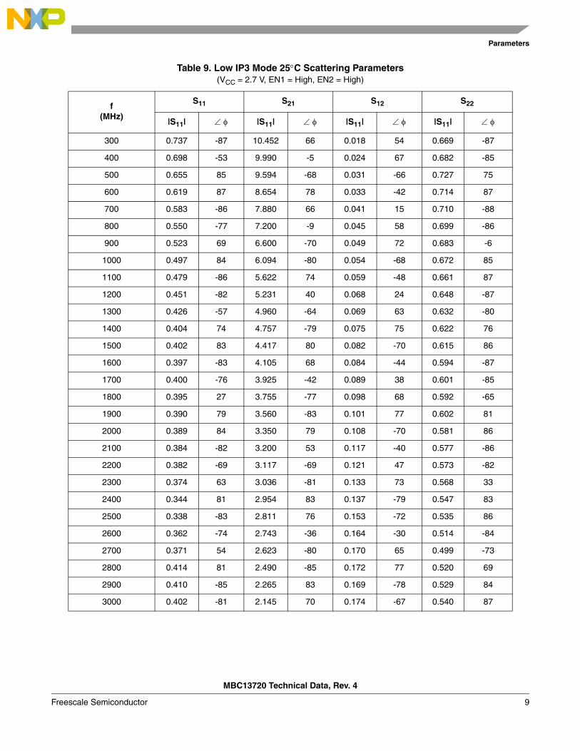
Table 9. Low IP3 Mode 25°C Scattering Parameters (VCC = 2.7 V, EN1 = High, EN2 = High)
f(MHz)
S11 S21 S12 S22
|S11| ∠ φ |S11| ∠ φ |S11| ∠ φ |S11| ∠ φ
300 0.737 -87 10.452 66 0.018 54 0.669 -87
400 0.698 -53 9.990 -5 0.024 67 0.682 -85
500 0.655 85 9.594 -68 0.031 -66 0.727 75
600 0.619 87 8.654 78 0.033 -42 0.714 87
700 0.583 -86 7.880 66 0.041 15 0.710 -88
800 0.550 -77 7.200 -9 0.045 58 0.699 -86
900 0.523 69 6.600 -70 0.049 72 0.683 -6
1000 0.497 84 6.094 -80 0.054 -68 0.672 85
1100 0.479 -86 5.622 74 0.059 -48 0.661 87
1200 0.451 -82 5.231 40 0.068 24 0.648 -87
1300 0.426 -57 4.960 -64 0.069 63 0.632 -80
1400 0.404 74 4.757 -79 0.075 75 0.622 76
1500 0.402 83 4.417 80 0.082 -70 0.615 86
1600 0.397 -83 4.105 68 0.084 -44 0.594 -87
1700 0.400 -76 3.925 -42 0.089 38 0.601 -85
1800 0.395 27 3.755 -77 0.098 68 0.592 -65
1900 0.390 79 3.560 -83 0.101 77 0.602 81
2000 0.389 84 3.350 79 0.108 -70 0.581 86
2100 0.384 -82 3.200 53 0.117 -40 0.577 -86
2200 0.382 -69 3.117 -69 0.121 47 0.573 -82
2300 0.374 63 3.036 -81 0.133 73 0.568 33
2400 0.344 81 2.954 83 0.137 -79 0.547 83
2500 0.338 -83 2.811 76 0.153 -72 0.535 86
2600 0.362 -74 2.743 -36 0.164 -30 0.514 -84
2700 0.371 54 2.623 -80 0.170 65 0.499 -73
2800 0.414 81 2.490 -85 0.172 77 0.520 69
2900 0.410 -85 2.265 83 0.169 -78 0.529 84
3000 0.402 -81 2.145 70 0.174 -67 0.540 87

Parameters
MBC13720 Technical Data, Rev. 4
10 Freescale Semiconductor
Table 10. Low IP3 Mode 85°C Scattering Parameters (VCC = 2.7 V, EN1 = High, EN2 = High)
f(MHz)
S11 S21 S12 S22
|S11| ∠ φ |S11| ∠ φ |S11| ∠ φ |S11| ∠ φ
300 0.722 -87 10.245 64 0.016 53 0.584 -86
400 0.681 -45 10.107 -8 0.025 66 0.650 -84
500 0.631 84 9.758 -69 0.030 -66 0.718 76
600 0.601 87 8.730 77 0.036 -47 0.709 87
700 0.564 -85 7.901 65 0.040 11 0.708 -88
800 0.534 -76 7.185 -15 0.046 60 0.690 -85
900 0.512 70 6.564 -71 0.051 72 0.680 1
1000 0.484 83 6.062 -80 0.056 -69 0.670 85
1100 0.467 -86 5.559 74 0.061 -45 0.657 87
1200 0.440 -82 5.165 36 0.066 18 0.646 -86
1300 0.415 -57 4.925 -65 0.072 62 0.628 -80
1400 0.394 74 4.700 -79 0.077 75 0.616 76
1500 0.391 83 4.348 80 0.084 -70 0.606 86
1600 0.389 -83 4.051 67 0.091 -46 0.586 -87
1700 0.388 -76 3.857 -45 0.097 37 0.594 -84
1800 0.381 16 3.689 -77 0.100 69 0.580 -62
1900 0.384 78 3.489 -83 0.107 77 0.589 81
2000 0.380 84 3.291 79 0.114 -71 0.571 86
2100 0.377 -82 3.139 52 0.122 -46 0.574 -86
2200 0.371 -72 3.049 -70 0.131 50 0.567 -82
2300 0.369 50 2.974 -82 0.139 74 0.562 41
2400 0.343 80 2.941 83 0.143 -79 0.540 83
2500 0.315 -83 2.771 76 0.157 -72 0.525 86
2600 0.323 -76 2.711 -30 0.167 -29 0.511 -84
2700 0.340 8 2.636 -79 0.174 63 0.519 -73
2800 0.382 77 2.521 -84 0.179 77 0.533 72
2900 0.410 -85 2.265 83 0.169 -78 0.529 84
3000 0.402 -81 2.145 70 0.174 -67 0.540 87
Parameters
MBC13720 Technical Data, Rev. 4
Freescale Semiconductor 11
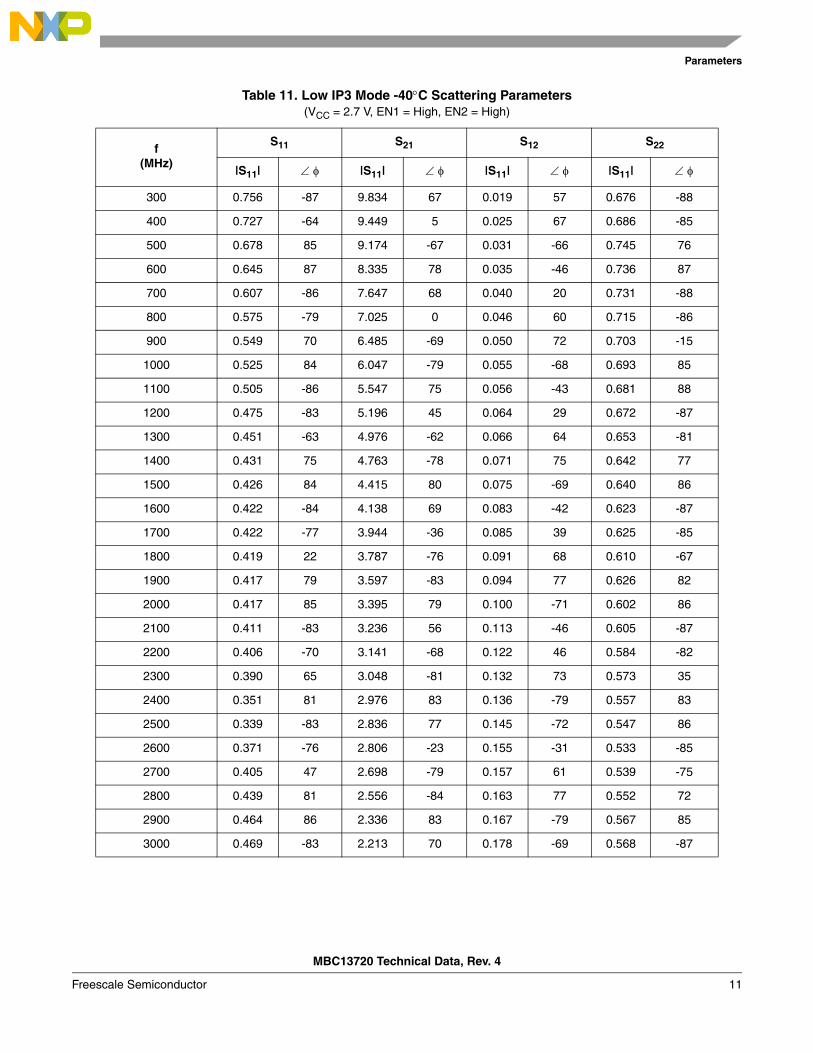
Table 11. Low IP3 Mode -40°C Scattering Parameters (VCC = 2.7 V, EN1 = High, EN2 = High)
f(MHz)
S11 S21 S12 S22
|S11| ∠ φ |S11| ∠ φ |S11| ∠ φ |S11| ∠ φ
300 0.756 -87 9.834 67 0.019 57 0.676 -88
400 0.727 -64 9.449 5 0.025 67 0.686 -85
500 0.678 85 9.174 -67 0.031 -66 0.745 76
600 0.645 87 8.335 78 0.035 -46 0.736 87
700 0.607 -86 7.647 68 0.040 20 0.731 -88
800 0.575 -79 7.025 0 0.046 60 0.715 -86
900 0.549 70 6.485 -69 0.050 72 0.703 -15
1000 0.525 84 6.047 -79 0.055 -68 0.693 85
1100 0.505 -86 5.547 75 0.056 -43 0.681 88
1200 0.475 -83 5.196 45 0.064 29 0.672 -87
1300 0.451 -63 4.976 -62 0.066 64 0.653 -81
1400 0.431 75 4.763 -78 0.071 75 0.642 77
1500 0.426 84 4.415 80 0.075 -69 0.640 86
1600 0.422 -84 4.138 69 0.083 -42 0.623 -87
1700 0.422 -77 3.944 -36 0.085 39 0.625 -85
1800 0.419 22 3.787 -76 0.091 68 0.610 -67
1900 0.417 79 3.597 -83 0.094 77 0.626 82
2000 0.417 85 3.395 79 0.100 -71 0.602 86
2100 0.411 -83 3.236 56 0.113 -46 0.605 -87
2200 0.406 -70 3.141 -68 0.122 46 0.584 -82
2300 0.390 65 3.048 -81 0.132 73 0.573 35
2400 0.351 81 2.976 83 0.136 -79 0.557 83
2500 0.339 -83 2.836 77 0.145 -72 0.547 86
2600 0.371 -76 2.806 -23 0.155 -31 0.533 -85
2700 0.405 47 2.698 -79 0.157 61 0.539 -75
2800 0.439 81 2.556 -84 0.163 77 0.552 72
2900 0.464 86 2.336 83 0.167 -79 0.567 85
3000 0.469 -83 2.213 70 0.178 -69 0.568 -87

Parameters
MBC13720 Technical Data, Rev. 4
12 Freescale Semiconductor
Table 12. Bypass Mode 25°C Scattering Parameters (VCC = 2.7 V, EN1 = Low, EN2 = High)
f(MHz)
S11 S21 S12 S22
|S11| ∠ φ |S11| ∠ φ |S11| ∠ φ |S11| ∠ φ
300 0.866 -88 0.293 76 0.295 76 0.706 -87
400 0.811 79 0.386 85 0.384 85 0.702 -81
500 0.753 87 0.468 -82 0.470 -82 0.736 85
600 0.717 -88 0.514 -2 0.506 6 0.710 88
700 0.671 -85 0.549 83 0.546 83 0.687 -87
800 0.629 29 0.575 87 0.575 87 0.653 -75
900 0.593 84 0.600 -85 0.604 -85 0.618 82
1000 0.556 87 0.615 -64 0.618 -64 0.585 86
1100 0.527 -84 0.624 83 0.626 83 0.555 -86
1200 0.492 -57 0.636 87 0.632 87 0.528 -79
1300 0.456 78 0.647 -87 0.641 -87 0.493 63
1400 0.435 85 0.655 -81 0.649 -81 0.474 83
1500 0.439 -83 0.648 76 0.652 77 0.470 -86
1600 0.440 -70 0.637 86 0.634 86 0.456 -81
1700 0.428 70 0.631 -87 0.628 -87 0.451 -40
1800 0.412 83 0.642 -85 0.626 -85 0.417 78
1900 0.395 -84 0.649 -54 0.641 -59 0.397 84
2000 0.396 -78 0.636 83 0.644 84 0.379 -82
2100 0.384 30 0.626 87 0.633 87 0.344 -68
2200 0.362 79 0.619 -86 0.623 -86 0.322 65
2300 0.346 84 0.622 -81 0.620 -81 0.294 80
2400 0.335 -78 0.615 72 0.610 72 0.274 -81
2500 0.368 -20 0.576 85 0.592 85 0.271 -69
2600 0.398 78 0.546 -87 0.554 -87 0.262 51
2700 0.415 84 0.535 -84 0.530 -84 0.231 76
2800 0.421 -84 0.532 -66 0.510 -66 0.199 -81
2900 0.415 -75 0.533 78 0.532 77 0.173 -73
3000 0.413 60 0.510 85 0.523 85 0.141 20
Parameters
MBC13720 Technical Data, Rev. 4
Freescale Semiconductor 13
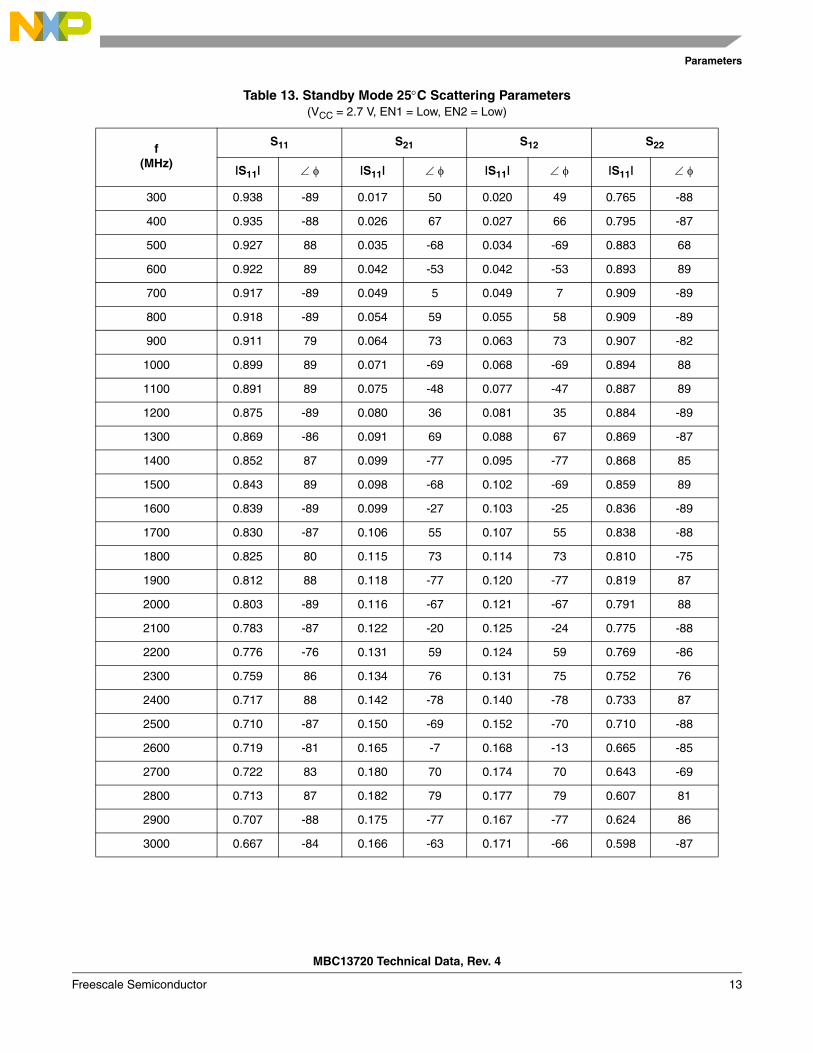
Table 13. Standby Mode 25°C Scattering Parameters (VCC = 2.7 V, EN1 = Low, EN2 = Low)
f(MHz)
S11 S21 S12 S22
|S11| ∠ φ |S11| ∠ φ |S11| ∠ φ |S11| ∠ φ
300 0.938 -89 0.017 50 0.020 49 0.765 -88
400 0.935 -88 0.026 67 0.027 66 0.795 -87
500 0.927 88 0.035 -68 0.034 -69 0.883 68
600 0.922 89 0.042 -53 0.042 -53 0.893 89
700 0.917 -89 0.049 5 0.049 7 0.909 -89
800 0.918 -89 0.054 59 0.055 58 0.909 -89
900 0.911 79 0.064 73 0.063 73 0.907 -82
1000 0.899 89 0.071 -69 0.068 -69 0.894 88
1100 0.891 89 0.075 -48 0.077 -47 0.887 89
1200 0.875 -89 0.080 36 0.081 35 0.884 -89
1300 0.869 -86 0.091 69 0.088 67 0.869 -87
1400 0.852 87 0.099 -77 0.095 -77 0.868 85
1500 0.843 89 0.098 -68 0.102 -69 0.859 89
1600 0.839 -89 0.099 -27 0.103 -25 0.836 -89
1700 0.830 -87 0.106 55 0.107 55 0.838 -88
1800 0.825 80 0.115 73 0.114 73 0.810 -75
1900 0.812 88 0.118 -77 0.120 -77 0.819 87
2000 0.803 -89 0.116 -67 0.121 -67 0.791 88
2100 0.783 -87 0.122 -20 0.125 -24 0.775 -88
2200 0.776 -76 0.131 59 0.124 59 0.769 -86
2300 0.759 86 0.134 76 0.131 75 0.752 76
2400 0.717 88 0.142 -78 0.140 -78 0.733 87
2500 0.710 -87 0.150 -69 0.152 -70 0.710 -88
2600 0.719 -81 0.165 -7 0.168 -13 0.665 -85
2700 0.722 83 0.180 70 0.174 70 0.643 -69
2800 0.713 87 0.182 79 0.177 79 0.607 81
2900 0.707 -88 0.175 -77 0.167 -77 0.624 86
3000 0.667 -84 0.166 -63 0.171 -66 0.598 -87

Parameters
MBC13720 Technical Data, Rev. 4
14 Freescale Semiconductor
Table 14. Low IP3 Noise Parameters (VCC = 2.7 V, EN1 = High, EN2 = High)
f (MHz) Fmin (dB) Mag Ang Rn Ga (dB)
400 0.57 0.26 15.5 0.19 25.3
410 0.57 0.26 15.7 0.19 24.93
420 0.58 0.26 16 0.19 24.8
430 0.58 0.26 16.2 0.19 24.68
440 0.59 0.26 16.5 0.19 24.56
450 0.59 0.26 16.7 0.19 24.44
460 0.59 0.26 16.9 0.19 24.32
470 0.6 0.26 17.2 0.19 24.2
480 0.6 0.26 17.4 0.19 24.09
490 0.6 0.26 17.7 0.19 23.97
500 0.61 0.26 17.9 0.19 23.85
550 0.63 0.26 19.1 0.19 23.01
600 0.64 0.26 20.3 0.19 22.59
650 0.66 0.25 21.5 0.19 22.16
700 0.67 0.25 22.7 0.19 21.74
750 0.69 0.25 23.9 0.19 21.32
800 0.7 0.25 25.1 0.19 20.89
850 0.72 0.24 26.4 0.19 20.47
900 0.73 0.24 27.6 0.19 20.05
1000 0.76 0.24 30 0.19 19.2
Table 15. High IP3 Noise Parameters (VCC = 2.7 V, EN1 = High, EN2 = Low)
f (MHz) Fmin (dB) Mag Ang Rn Ga (dB)
400 0.65 0.2 5.5 0.22 26.21
410 0.65 0.2 6.1 0.22 26.06
420 0.65 0.2 6.7 0.22 25.91
430 0.66 0.19 7.3 0.21 25.76
440 0.66 0.19 7.9 0.21 25.61
450 0.66 0.19 8.5 0.21 25.46
460 0.66 0.19 9.1 0.21 25.31
470 0.66 0.19 9.7 0.21 25.16

Parameters
MBC13720 Technical Data, Rev. 4
Freescale Semiconductor 15
Figure 2. Noise Figure vs Temperature (Low IP3 Mode)
480 0.67 0.18 10.3 0.2 25.01
490 0.67 0.18 10.9 0.2 24.87
500 0.67 0.18 11.5 0.2 24.54
550 0.68 0.17 14.5 0.19 24.06
600 0.69 0.16 17.5 0.19 23.59
650 0.7 0.15 20.5 0.18 23.12
700 0.71 0.14 23.5 0.18 22.65
750 0.72 0.13 26.5 0.17 22.17
800 0.73 0.12 29.4 0.17 21.7
850 0.74 0.11 32.4 0.16 21.23
900 0.75 0.1 35.4 0.16 20.76
1000 0.77 0.09 41.4 0.15 19.81
Table 15. High IP3 Noise Parameters (continued) (VCC = 2.7 V, EN1 = High, EN2 = Low)
f (MHz) Fmin (dB) Mag Ang Rn Ga (dB)

Parameters
MBC13720 Technical Data, Rev. 4
16 Freescale Semiconductor
Figure 3. Noise Figure vs Temperature (High IP3 Mode)
Figure 4. Icc vs Vcc Over Temperature (Low IP3 Mode)
Figure 5. Icc vs Vcc Over Temperature (High IP3 Mode)
Application Information
MBC13720 Technical Data, Rev. 4
Freescale Semiconductor 17
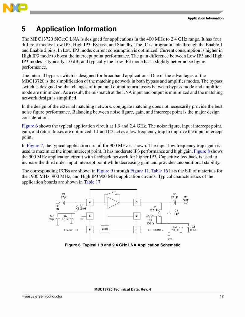
5 Application InformationThe MBC13720 SiGe:C LNA is designed for applications in the 400 MHz to 2.4 GHz range. It has four different modes: Low IP3, High IP3, Bypass, and Standby. The IC is programmable through the Enable 1 and Enable 2 pins. In Low IP3 mode, current consumption is optimized. Current consumption is higher in High IP3 mode to boost the intercept point performance. The gain difference between Low IP3 and High IP3 modes is typically 1.0 dB; and typically the Low IP3 mode has a slightly better noise figure performance.
The internal bypass switch is designed for broadband applications. One of the advantages of the MBC13720 is the simplification of the matching network in both bypass and amplifier modes. The bypass switch is designed so that changes of input and output return losses between bypass mode and amplifier mode are minimized. As a result, the mismatch at the LNA input and output is minimized and the matching network design is simplified.
In the design of the external matching network, conjugate matching does not necessarily provide the best noise figure performance. Balancing between noise figure, gain, and intercept point is the major design consideration.
Figure 6 shows the typical application circuit at 1.9 and 2.4 GHz. The noise figure, input intercept point, gain, and return losses are optimized. L1 and C2 act as a low frequency trap to improve the input intercept point.
In Figure 7, the typical application circuit for 900 MHz is shown. The input low frequency trap again is used to maximize the input intercept point. It has moderate IP3 performance and high gain. Figure 8 shows the 900 MHz application circuit with feedback network for higher IP3. Capacitive feedback is used to increase the third order input intercept point while decreasing gain and provides unconditional stability.
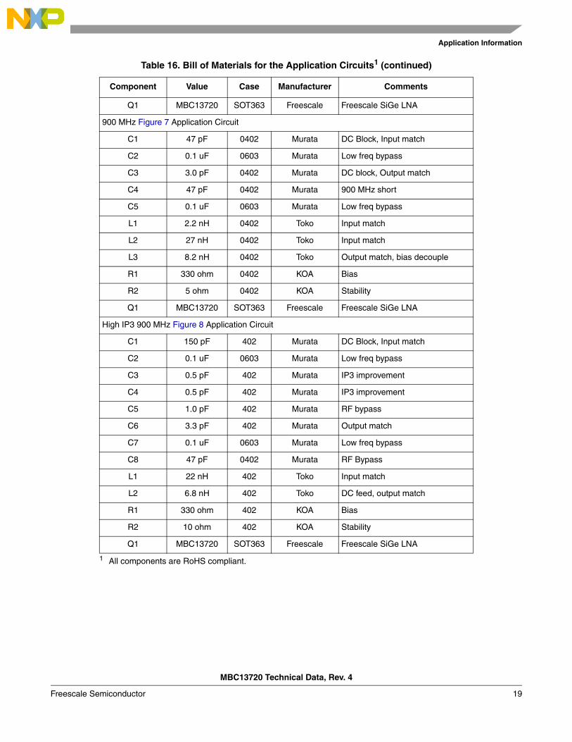
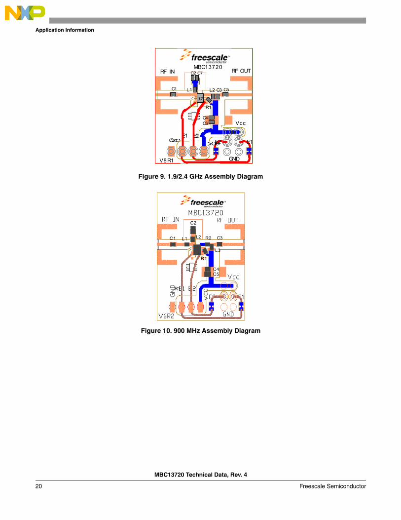
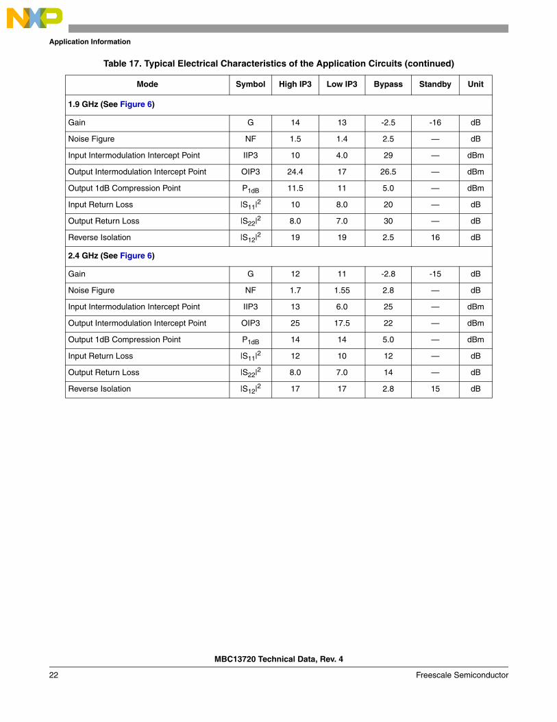
The corresponding PCBs are shown in Figure 9 through Figure 11. Table 16 lists the bill of materials for the 1900 MHz, 900 MHz, and High IP3 900 MHz application circuits. Typical characteristics of the application boards are shown in Table 17.
Figure 6. Typical 1.9 and 2.4 GHz LNA Application Schematic
2
1
34
5
6
RF IN
RF OUT
Enable2
Vcc
R1330 Ω
L22.7 nH
C527 pF
C1 27pf
L1 8.2 nH
C2 0.1 uF
C433 pFEnable1
C60.1uFLogic
C7 33 pF
C31 pF

Application Information
MBC13720 Technical Data, Rev. 4
18 Freescale Semiconductor
Figure 7. Typical 900 MHz LNA Application Schematic
Figure 8. High IP3 900 MHz LNA Application Schematic
Table 16. Bill of Materials for the Application Circuits1
Component Value Case Manufacturer Comments
1900 MHz Figure 6 Application Circuit
C1 27 pF 0402 Murata DC Block, Input match
C2 0.1 uF 0603 Murata Low freq bypass
C3 1.0 pF 0402 Murata Output match
C4 33 pF 0402 Murata Low freq bypass
C5 27 pF 0402 Murata DC Block, Output match
C6 0.1 uF 0603 Murata Low freq bypass
C7 33 pF 0402 Murata RF bypass
L1 8.2 nH 0402 Toko Low freq bypass
L2 2.7 nH 0402 Toko DC feed, Output match
R1 330 ohm 0402 KOA Bias
2
1
34
5
6
RF IN
R25 Ω RF
OUT
Enable2
Vcc
R1330 Ω
L38.2 nH
C33 pF
C1 47pF
L2 27 nH
C2 0.1 uF
C447 pFEnable1
C50.1 uF
L1 2.2 nH
Logic
2
1
34
5
6
RF IN
R210 Ω RF
OUT
Enable2
Vcc
R1330 Ω
L26.8 nH
C63.3 pF
C1 150pF
L1 22 nH
pp
C2 0.1 uF
C70.1 uF
p
Enable1C8
47 pFLogic
Application Information
MBC13720 Technical Data, Rev. 4
Freescale Semiconductor 19
Q1 MBC13720 SOT363 Freescale Freescale SiGe LNA
900 MHz Figure 7 Application Circuit
C1 47 pF 0402 Murata DC Block, Input match
C2 0.1 uF 0603 Murata Low freq bypass
C3 3.0 pF 0402 Murata DC block, Output match
C4 47 pF 0402 Murata 900 MHz short
C5 0.1 uF 0603 Murata Low freq bypass
L1 2.2 nH 0402 Toko Input match
L2 27 nH 0402 Toko Input match
L3 8.2 nH 0402 Toko Output match, bias decouple
R1 330 ohm 0402 KOA Bias
R2 5 ohm 0402 KOA Stability
Q1 MBC13720 SOT363 Freescale Freescale SiGe LNA
High IP3 900 MHz Figure 8 Application Circuit
C1 150 pF 402 Murata DC Block, Input match
C2 0.1 uF 0603 Murata Low freq bypass
C3 0.5 pF 402 Murata IP3 improvement
C4 0.5 pF 402 Murata IP3 improvement
C5 1.0 pF 402 Murata RF bypass
C6 3.3 pF 402 Murata Output match
C7 0.1 uF 0603 Murata Low freq bypass
C8 47 pF 0402 Murata RF Bypass
L1 22 nH 402 Toko Input match
L2 6.8 nH 402 Toko DC feed, output match
R1 330 ohm 402 KOA Bias
R2 10 ohm 402 KOA Stability
Q1 MBC13720 SOT363 Freescale Freescale SiGe LNA
1 All components are RoHS compliant.
Table 16. Bill of Materials for the Application Circuits1 (continued)
Component Value Case Manufacturer Comments
Application Information
MBC13720 Technical Data, Rev. 4
20 Freescale Semiconductor
Figure 9. 1.9/2.4 GHz Assembly Diagram
Figure 10. 900 MHz Assembly Diagram
L1
C2
C3L2C1
C4
R1
C5
C6
C7RF IN RF OUT
V8R1 GND
Vcc
MBC13720
G N D E1E2E1
E2V C C
Q1
C1
C2
C3
R1
L1 L2
R1
R2
C4C5
L3

Application Information
MBC13720 Technical Data, Rev. 4
Freescale Semiconductor 21
Figure 11. 900 MHz Capacitive Feedback Assembly Diagram
Table 17. Typical Electrical Characteristics of the Application Circuits
Mode Symbol High IP3 Low IP3 Bypass Standby Unit
900 MHz TYPICAL (See Figure 7)
Gain G 20 19 -2.9 -22 dB
Noise Figure NF 1.3 1.2 2.9 — dB
Input Intermodulation Intercept Point IIP3 2.0 -3.0 29 — dBm
Output Intermodulation Intercept Point OIP3 23 17 26 — dBm
Output 1dB Compression Point P1dB 11.5 10.5 5.0 — dBm
Input Return Loss |S11|2 11 10 12 — dB
Output Return Loss |S22|2 11 10 15 — dB
Reverse Isolation |S12|2 25 24 2.9 22 dB
900 MHz HIGH IP3 (See Figure 8)
Gain G 16 15 -4.0 -14.5 dB
Noise Figure NF 1.4 1.3 4.0 — dB
Input Intermodulation Intercept Point IIP3 10 2.0 27 — dBm
Output Intermodulation Intercept Point OIP3 26 18.5 23 — dBm
Output 1 dB Compression Point P1dB 11.5 12 5.0 — dBm
Input Return Loss |S11|2 12 11 8.0 — dB
Output Return Loss |S22|2 12 12 14 — dB
Reverse Isolation |S12|2 22 20 4.0 14.5 dB
C1
C2C3 C4C5
C6
C7
L1
L2
R1
R2
Application Information
MBC13720 Technical Data, Rev. 4
22 Freescale Semiconductor
1.9 GHz (See Figure 6)
Gain G 14 13 -2.5 -16 dB
Noise Figure NF 1.5 1.4 2.5 — dB
Input Intermodulation Intercept Point IIP3 10 4.0 29 — dBm
Output Intermodulation Intercept Point OIP3 24.4 17 26.5 — dBm
Output 1dB Compression Point P1dB 11.5 11 5.0 — dBm
Input Return Loss |S11|2 10 8.0 20 — dB
Output Return Loss |S22|2 8.0 7.0 30 — dB
Reverse Isolation |S12|2 19 19 2.5 16 dB
2.4 GHz (See Figure 6)
Gain G 12 11 -2.8 -15 dB
Noise Figure NF 1.7 1.55 2.8 — dB
Input Intermodulation Intercept Point IIP3 13 6.0 25 — dBm
Output Intermodulation Intercept Point OIP3 25 17.5 22 — dBm
Output 1dB Compression Point P1dB 14 14 5.0 — dBm
Input Return Loss |S11|2 12 10 12 — dB
Output Return Loss |S22|2 8.0 7.0 14 — dB
Reverse Isolation |S12|2 17 17 2.8 15 dB
Table 17. Typical Electrical Characteristics of the Application Circuits (continued)
Mode Symbol High IP3 Low IP3 Bypass Standby Unit

NOTES
MBC13720 Technical Data, Rev. 4
Freescale Semiconductor 23
6 Packaging
Figure 12. Outline Dimensions for SOT-363 (Case Outline 419B-01, Issue G)
7 Product DocumentationThis data sheet is labeled as a particular type: Product Preview, Advance Information, or Technical Data. Definitions of these types are available at: http://www.freescale.com on the documentation page.
Table 18 summarizes revisions to this document since the previous release (Rev. 3.5).
Table 18. Revision History
Location Revision
Section 3, “Electrical Specifications Added Note about Maximum ratings and ESD specifications.
Figure 6 through Figure 8 Updated figure content
M0.2 (0.008) B M
1 2 3
A
GV
S
6 5 4
-B-
D 6 PL
NOTES: 1. DIMENSIONING AND TOLERANCING PER ANSI
Y14.5M, 1982. 2. CONTROLLING DIMENSION: INCH.
DIM MIN MAX MIN MAXMILLIMETERSINCHES
A 1.80 2.200.071 0.087B 1.15 1.350.045 0.053C 0.80 1.100.031 0.043D 0.10 0.300.004 0.012G 0.65 BSC0.026 BSCH --- 0.10---0.004J 0.10 0.250.004 0.010K 0.10 0.300.004 0.012N 0.20 REF0.008 REFS 2.00 2.200.079 0.087V 0.30 0.400.012 0.016
H
C
N
J
K

Document Number: MBC13720Rev. 409/2011
How to Reach Us:
Home Page:www.freescale.com
E-mail:[email protected]
USA/Europe or Locations Not Listed:Freescale SemiconductorTechnical Information Center, CH3701300 N. Alma School RoadChandler, Arizona 85224+1-800-521-6274 or [email protected]
Europe, Middle East, and Africa:Freescale Halbleiter Deutschland GmbHTechnical Information CenterSchatzbogen 781829 Muenchen, Germany+44 1296 380 456 (English)+46 8 52200080 (English)+49 89 92103 559 (German)+33 1 69 35 48 48 (French)[email protected]
Japan:Freescale Semiconductor Japan Ltd.HeadquartersARCO Tower 15F1-8-1, Shimo-Meguro, Meguro-ku,Tokyo 153-0064, Japan0120 191014 or +81 3 5437 [email protected]
Asia/Pacific:Freescale Semiconductor Hong Kong Ltd.Technical Information Center2 Dai King StreetTai Po Industrial EstateTai Po, N.T., Hong Kong+800 2666 [email protected]
For Literature Requests Only:Freescale Semiconductor Literature Distribution CenterP.O. Box 5405Denver, Colorado 802171-800-521-6274 or 303-675-2140Fax: [email protected]
Information in this document is provided solely to enable system and software implementers to use Freescale Semiconductor products. There are no express or implied copyright licenses granted hereunder to design or fabricate any integrated circuits or integrated circuits based on the information in this document.
Freescale Semiconductor reserves the right to make changes without further notice to any products herein. Freescale Semiconductor makes no warranty, representation or guarantee regarding the suitability of its products for any particular purpose, nor does Freescale Semiconductor assume any liability arising out of the application or use of any product or circuit, and specifically disclaims any and all liability, including without limitation consequential or incidental damages. “Typical” parameters that may be provided in Freescale Semiconductor data sheets and/or specifications can and do vary in different applications and actual performance may vary over time. All operating parameters, including “Typicals”, must be validated for each customer application by customer’s technical experts. Freescale Semiconductor does not convey any license under its patent rights nor the rights of others. Freescale Semiconductor products are not designed, intended, or authorized for use as components in systems intended for surgical implant into the body, or other applications intended to support or sustain life, or for any other application in which the failure of the Freescale Semiconductor product could create a situation where personal injury or death may occur. Should Buyer purchase or use Freescale Semiconductor products for any such unintended or unauthorized application, Buyer shall indemnify and hold Freescale Semiconductor and its officers, employees, subsidiaries, affiliates, and distributors harmless against all claims, costs, damages, and expenses, and reasonable attorney fees arising out of, directly or indirectly, any claim of personal injury or death associated with such unintended or unauthorized use, even if such claim alleges that Freescale Semiconductor was negligent regarding the design or manufacture of the part.
Freescale™ and the Freescale logo are trademarks of Freescale Semiconductor, Inc. All other product or service names are the property of their respective owners.
© Freescale Semiconductor, Inc. 2005–2011. All rights reserved.
RoHS-compliant and/or Pb-free versions of Freescale products have the functionality and electrical characteristics of their non-RoHS-compliant and/or non-Pb-free counterparts. For further information, see http://www.freescale.com or contact your Freescale sales representative.
For information on Freescale’s Environmental Products program, go to http://www.freescale.com/epp.