d16_06r4
TRANSCRIPT
300 • 2015 IEEE International Solid-State Circuits Conference
ISSCC 2015 / SESSION 16 / EMERGING TECHNOLOGIES ENABLING NEXT-GENERATION SYSTEMS / 16.6
16.6 A Double-Side CMOS-CNT Biosensor Array with Padless Structure for Simple Bare-Die Measurements in a Medical Environment
Jinhong Ahn1, Jeaheung Lim1, Seok-Hyang Kim1, Jun-Yeon Yun1, Changhyun Kim1, Sang-Hoon Hong2, Myoung-Jin Lee3, Youngjune Park1
1Seoul National University, Seoul, Korea, 2Kyung Hee University, Yongin, Korea, 3Chonnam National University, Gwangju, Korea
CMOS sensors using nanomaterials on the surface are very effective for earlydetection of diseases. Among the nanomaterials, carbon nanotube (CNT) is anideal biosensor material since it has a small diameter (~1nm) directly comparable to the size of biomolecules and excellent electrical characteristics.Because CNT is formed chemically in a special environment, to use it in a CMOSprocess, many electrodes are formed as an array and the CNT solution is coatedon the electrode array. However, to prevent electrical shorts between bondingpads, very complicated area-selective CNT coating processes are required.Furthermore, chip packaging steps—such as wire bonding, chip passivationagainst reactions to the wire, microfluidic channels on the chip, etc.—should becarefully applied [1].
Double-sided chips can be a solution to these problems because it does not havepads on the surface and it’s directly measurable without packaging. A double-sided chip using through-silicon via process for RFID was reported, where a silicon-on-insulator wafer is used to avoid latch-up failure [2]. However, formedical applications, which are mostly one-time usage, more cost-effectivesolutions are desired.
To address these issues, this paper presents a double-sided CMOS-CNT sensorarray based on a 0.35μm standard CMOS process. This scheme allows robustmeasurements due to its inherent rectifying diodes with a high latch-up resistance. In particular, instead of pads, there are just two contact metal structures. A wide ring structure around the sensor area on the front side and aplate structure at the backside are used for both power and single I/O line, wherethe other power is extracted from a “high” state of I/O line signals using the rectifier. In order to implement these special functions, a controller chip with aspecial I/O protocol is designed. Using this controller chip, issuing commandsand receiving data can both be performed on a single line, and the results areflexibly measured on either the backside or the front side of the chip. As a result,a stable operation under 150mW sensing power at 2MHz data rate can beachieved.
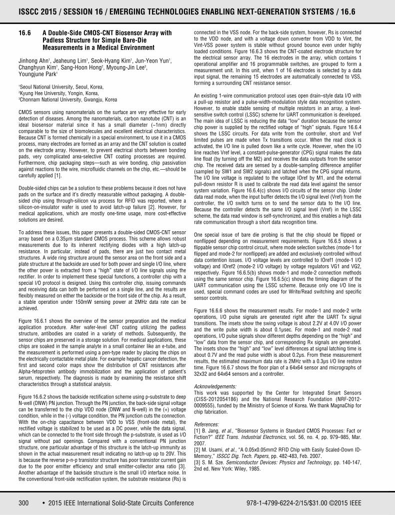
Figure 16.6.1 shows the overview of the sensor preparation and the medicalapplication procedure. After wafer-level CNT coating utilizing the padless structure, antibodies are coated in a variety of methods. Subsequently, the sensor chips are preserved in a storage solution. For medical applications, thesechips are soaked in the sample analyte in a small container like an e-tube, andthe measurement is performed using a pen-type reader by placing the chips onthe electrically contactable metal plate. For example hepatic cancer detection, thefirst and second color maps show the distribution of CNT resistances afterAlpha-fetoprotein antibody immobilization and the application of patient’sserum, respectively. The diagnosis is made by examining the resistance shiftcharacteristics through a statistical analysis.
Figure 16.6.2 shows the backside rectification scheme using p-substrate to deepN-well (DNW) PN junction. Through the PN junction, the back-side signal voltagecan be transferred to the chip VDD node (DNW and N-well) in the (+) voltagecondition, while in the (-) voltage condition, the PN junction cuts the connection.With the on-chip capacitance between VDD to VSS (front-side metal), the rectified voltage is stabilized to be used as a DC power, while the data signal,which can be connected to the front side through the p-substrate, is used as I/Osignal without pad openings. Compared with a conventional PN junction structure, one particular advantage of this structure is the latch-up immunity asshown in the actual measurement result indicating no latch-up up to 20V. Thisis because the reverse p-n-p transistor structure has poor transistor current gaindue to the poor emitter efficiency and small emitter-collector area ratio [3].Another advantage of the backside structure is the small I/O interface noise. Inthe conventional front-side rectification system, the substrate resistance (Rs) is
connected in the VSS node. For the back-side system, however, Rs is connectedto the VDD node, and with a voltage down converter from VDD to Vint, the Vint-VSS power system is stable without ground bounce even under highlyloaded conditions. Figure 16.6.3 shows the CNT-coated electrode structure forthe electrical sensor array. The 16 electrodes in the array, which contains 1 operational amplifier and 16 programmable switches, are grouped to form ameasurement unit. In this unit, when 1 of 16 electrodes is selected by a datainput signal, the remaining 15 electrodes are automatically connected to VSS,forming a surrounding CNT resistance sensor.
An existing 1-wire communication protocol uses open drain–style data I/O witha pull-up resistor and a pulse-width-modulation style data recognition system.However, to enable stable sensing of multiple resistors in an array, a level-sensitive switch control (LSSC) scheme for UART communication is developed.The main idea of LSSC is reducing the data “low” duration because the sensorchip power is supplied by the rectified voltage of “high” signals. Figure 16.6.4shows the LSSC circuits. For data write from the controller, short and Vref limited pulses are made when Tx transitions occur. When the read clock is activated, the I/O line is pulled down like a write cycle. However, when the I/Oline reaches Vref level, a constant-pulse-generator (CPG) signal makes the dataline float (by turning off the M2) and receives the data outputs from the sensorchip. The received data are sensed by a double-sampling difference amplifier(sampled by SW1 and SW2 signals) and latched when the CPG signal returns.The I/O line voltage is regulated to the voltage IOref by M1, and the external pull-down resistor R is used to calibrate the read data level against the sensorsystem variation. Figure 16.6.4(c) shows I/O circuits of the sensor chip. Underdata read mode, when the input buffer detects the I/O signal level (Vref) from thecontroller, the I/O switch turns on to send the sensor data to the I/O line.Because the controller detects the same I/O signal level (Vref) in the LSSCscheme, the data read window is self-synchronized, and this enables a high datarate communication through a short data recognition time.
One special issue of bare die probing is that the chip should be flipped or nonflipped depending on measurement requirements. Figure 16.6.5 shows aflippable sensor chip control circuit, where mode selection switches (mode-1 forflipped and mode-2 for nonflipped) are added and exclusively controlled withoutdata contention issues. I/O voltage levels are controlled to IOref1 (mode-1 I/Ovoltage) and IOref2 (mode-2 I/O voltage) by voltage regulators VG1 and VG2,respectively. Figure 16.6.5(b) shows mode-1 and mode-2 connection methodsusing the same sensor chip. Figure 16.6.5(c) shows the timing diagram of theUART communication using the LSSC scheme. Because only one I/O line isused, special command codes are used for Write/Read switching and specificsensor controls.
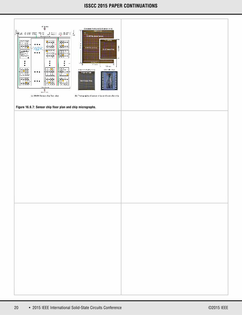
Figure 16.6.6 shows the measurement results. For mode-1 and mode-2 writeoperations, I/O pulse signals are generated right after the UART Tx signal transitions. The insets show the swing voltage is about 2.2V at 4.0V I/O powerand the write pulse width is about 0.1μsec. For mode-1 and mode-2 read operations, I/O pulse signals show different depths depending on the “high” and“low” data from the sensor chip, and corresponding Rx signals are generated.The insets show the “high” and “low” level differences at signal latching time isabout 0.7V and the read pulse width is about 0.2μs. From these measurementresults, the estimated maximum data rate is 2MHz with a 0.3μs I/O line restoretime. Figure 16.6.7 shows the floor plan of a 64x64 sensor and micrographs of32x32 and 64x64 sensors and a controller.
Acknowledgements:This work was supported by the Center for Integrated Smart Sensors (CISS-2012054186) and the National Research Foundation (NRF-2012-0009555), funded by the Ministry of Science of Korea. We thank MagnaChip forchip fabrication.
References:[1] B. Jang, et al., “Biosensor Systems in Standard CMOS Processes: Fact orFiction?” IEEE Trans. Industrial Electronics, vol. 56, no. 4, pp. 979–985, Mar.2007.[2] M. Usami, et al., “A 0.05x0.05mm2 RFID Chip with Easily Scaled-Down ID-Memory,” ISSCC Dig. Tech. Papers, pp. 482-483, Feb. 2007.[3] S. M. Sze. Semiconductor Devices: Physics and Technology, pp. 140-147,2nd ed. New York: Wiley, 1985.
978-1-4799-6224-2/15/$31.00 ©2015 IEEE
301DIGEST OF TECHNICAL PAPERS •
ISSCC 2015 / February 24, 2015 / 3:45 PM
Figure 16.6.1: Overview of sensor preparation and medical applicationprocedures.
Figure 16.6.2: Simplified structure of backside rectification and advantagesover conventional rectification.
Figure 16.6.3: Sensor electrode structure and surrounding CNT resistance formation.
Figure 16.6.5: Mode control schemes for flippable measurement and LSSCtiming diagram.
Figure 16.6.6: Measurement results of Write/Read signals for mode-1 andmode-2 connections.
Figure 16.6.4: Circuit schematics of level-sensitive switch control (LSSC)scheme.
16
20 • 2015 IEEE International Solid-State Circuits Conference ©2015 IEEE
ISSCC 2015 PAPER CONTINUATIONS
Figure 16.6.7: Sensor chip floor plan and chip micrographs.