course manual - 2010
TRANSCRIPT

8/6/2019 Course Manual - 2010
http://slidepdf.com/reader/full/course-manual-2010 1/71
HPES Course MaterialEmbedded Systems & Robotics
2010
Sourabh Sankulewww.sourabh.sankule.com
June 2010

8/6/2019 Course Manual - 2010
http://slidepdf.com/reader/full/course-manual-2010 2/71
2 | P a g e Course material designed by Sourabh Sankule | www.sourabh.sankule.com
Contribution
Arpit Mathur
Abhijeet Gupta
Ankur Agrawal
Tanmay Gangwani
Acknowledgement
Robocon Team, IIT Kanpur
Robotics Club, IIT Kanpur
Electronics Club, IIT Kanpur
Centre for Mechatronics, IIT Kanpur

8/6/2019 Course Manual - 2010
http://slidepdf.com/reader/full/course-manual-2010 3/71
3 | P a g e Course material designed by Sourabh Sankule | www.sourabh.sankule.com
Contents
Section A: Digital Electronics
Chapter 1 Basics ........................................................................................... 8
1.1 What is a Digital system? .................................................................................................... 8
1.2 Assigning States .................................................................................................................. 81.3 Number Systems in digital electronics................................................................................ 8
1.4 Types of Digital Circuits ....................................................................................................... 8
1.5 Clock: Building block of a sequential circuit ....................................................................... 9
1.6 Logic Gates: Building block of a combinatorial circuitry ..................................................... 9
1.7 Practical Circuiting Elements ............................................................................................ 10
1.7.1 Resistor: .................................................................................................................... 10
1.7.2 Capacitor: .................................................................................................................. 10
1.7.3 Breadboard: .............................................................................................................. 111.7.4 Integrated Circuits (IC) .............................................................................................. 11
1.7.5 LED ............................................................................................................................ 12
Chapter 2 Some Integrated Circuits and Implementation ........................... 13
2.1 555 .................................................................................................................................... 13
2.1.1 Monostable mode..................................................................................................... 13
2.1.2 Astable mode ............................................................................................................ 14
2.2 4029 counter ..................................................................................................................... 15
2.2.1 Pin Description .......................................................................................................... 152.3 7447: BCD to 7 segment display decoder ......................................................................... 16
2.3.1 Pin Description .......................................................................................................... 16
2.4 LDR (Light Dependent Resistor) ........................................................................................ 17
2.5 Operational Amplifier (Opamp) ........................................................................................ 17
2.5.1 Opamp as a comparator ........................................................................................... 18
2.6 7805 Voltage Regulator .................................................................................................... 18
8/6/2019 Course Manual - 2010
http://slidepdf.com/reader/full/course-manual-2010 4/71
4 | P a g e Course material designed by Sourabh Sankule | www.sourabh.sankule.com
Section B : Embedded Systems
Chapter 3 Introduction to Embedded Systems ........................................... 20
3.1 Applications ...................................................................................................................... 21
Chapter 4 Introduction to Microcontrollers ................................................ 22
4.1 Compiler / IDE (Integrated Development Environment) .................................................. 24
4.2 Programmer ...................................................................................................................... 24
4.3 How to use Serial Programmer's Circuit (Hardware) ........................................................ 25
4.3.1 Software .................................................................................................................... 26
4.3.2 At-Prog ...................................................................................................................... 26
4.3.3 Pony Prog .................................................................................................................. 274.4 USB Programmer .............................................................................................................. 29
Chapter 5 Code Vision AVR (CVAVR) ........................................................... 30
5.1 CHIP: .................................................................................................................................. 31
5.2 PORT: ................................................................................................................................ 32
Chapter 6 Introduction to Atmega 16 Microcontroller ............................... 33
6.1 Features ............................................................................................................................ 33
6.2 Pin Configuration .............................................................................................................. 33
6.3 Block Diagram ................................................................................................................... 34
6.4 Pin Descriptions ................................................................................................................ 35
6.5 Digital Input Output Port .................................................................................................. 36
6.6 Registers............................................................................................................................ 36
Chapter 7 I/O Ports: .................................................................................... 37
7.1 DDRX (Data Direction Register) ........................................................................................ 37
7.2 PORTX (PORTX Data Register) ........................................................................................... 38
7.2.1 Output Pin ................................................................................................................. 38
7.2.2 Input Pin .................................................................................................................... 38
7.3 PINX (Data Read Register)................................................................................................. 39
Chapter 8 LCD Interfacing ........................................................................... 40
8.1 Overview of LCD Display ................................................................................................... 40
8.1.1 BLOCK DIAGRAM OF LCD DISPLAY: ........................................................................... 41
8.2 Circuit Connection ............................................................................................................ 42
8.3 Setting up in Microcontroller ............................................................................................ 43
8.4 Printing Functions ............................................................................................................. 44
8.4.1 lcd_clear() ................................................................................................................. 44
8.4.2 lcd_gotoxy(x,y) .......................................................................................................... 44

8/6/2019 Course Manual - 2010
http://slidepdf.com/reader/full/course-manual-2010 5/71
5 | P a g e Course material designed by Sourabh Sankule | www.sourabh.sankule.com
8.4.3 lcd_putchar(char c) ................................................................................................... 44
8.4.4 lcd_putsf(constant string) ......................................................................................... 44
8.4.5 lcd_puts(char arr) ..................................................................................................... 44
8.4.6 itoa(int val, char arr[]) ............................................................................................... 44
8.4.7 ftoa(float val, char decimal_places, char arr[]) ......................................................... 45
Chapter 9 UART Communication ................................................................ 46
9.1 UART: Theory of Operation .............................................................................................. 46
9.2 Serial Port of Computer .................................................................................................... 47
9.3 Setting up UART in microcontroller .................................................................................. 48
9.3.1 putchar() ................................................................................................................... 49
9.3.2 getchar() .................................................................................................................... 49
9.3.3 putsf() ........................................................................................................................ 49
9.4 Docklight ........................................................................................................................... 50
Chapter 10 Timers .................................................................................... 51
10.1 Basic Theory .................................................................................................................. 51
10.2 Fast PWM Mode ........................................................................................................... 52
10.3 CTC Mode ...................................................................................................................... 53
Chapter 11 SPI: Serial Peripheral Interface ............................................... 54
11.1 Theory of Operation ..................................................................................................... 54
11.2 Setting up SPI in Microcontroller .................................................................................. 55
11.2.1 Master Microcontroller ........................................................................................ 55
11.2.2 Slave Microcontroller ............................................................................................ 5511.3 Data Functions .............................................................................................................. 55
11.3.1 Transmit Data........................................................................................................ 55
11.3.2 Receive Data ......................................................................................................... 55
Chapter 12 ADC: Analog to Digital Converter ........................................... 56
12.1 Theory of operation ...................................................................................................... 56
12.2 Setting up Microcontroller............................................................................................ 56
12.3 Function for getting ADC .............................................................................................. 57
Chapter 13 Interrupts ............................................................................... 58 Example .................................................................................................................................. 58
13.1 Polling ........................................................................................................................... 58
13.2 Hardware interrupt ....................................................................................................... 58
13.3 Hardware Interrupt or polling? ..................................................................................... 58
13.4 Setting up Hardware Interrupt in Microcontroller ....................................................... 59
13.5 Functions of Interrupt Service Routine ......................................................................... 59

8/6/2019 Course Manual - 2010
http://slidepdf.com/reader/full/course-manual-2010 6/71
6 | P a g e Course material designed by Sourabh Sankule | www.sourabh.sankule.com
Section C: Robotics
Chapter 14 Introduction to Autonomous Robots ...................................... 61
14.1 Robot Chassis Designing ............................................................................................... 61
14.1.1 Robot with steering wheel: ................................................................................... 61
14.1.2 Robot with differential drive: ............................................................................... 62
Chapter 15 Motors and Motor Drivers ..................................................... 64 15.1 Introduction to Motors ................................................................................................. 64
15.2 H- Bridge: ...................................................................................................................... 65
15.3 Motor Driver ICs: L293/L293D and L298....................................................................... 66
15.3.1 Difference between L293 and L298: ..................................................................... 67
15.3.2 Speed Control: ...................................................................................................... 67
Chapter 16 Sensors ................................................................................... 68
16.1 Analog Sensor ............................................................................................................... 68
16.2 Digital IR Sensor - TSOP Sensor ..................................................................................... 69
Chapter 17 Project Work .......................................................................... 70
17.1 Line following Robot ..................................................................................................... 70
Chapter 18 References ............................................................................. 71

8/6/2019 Course Manual - 2010
http://slidepdf.com/reader/full/course-manual-2010 7/71
7 | P a g e Course material designed by Sourabh Sankule | www.sourabh.sankule.com
Section A
Digital Electronics

8/6/2019 Course Manual - 2010
http://slidepdf.com/reader/full/course-manual-2010 8/71
8 | P a g e Course material designed by Sourabh Sankule | www.sourabh.sankule.com
Chapter 1 Basics
1.1 What is a Digital system?
In most general terms, this system’s behavior is sufficiently explained by using only two of itsstates can be Voltage(more than x volts or less?),distance covered(more than 2.5 km or less?],true-
false or weight of an elephant(will my weighing machine withstand it?) )
Note that although in every case, the all the intermediate states ARE POSSIBLE AND DO EXIST, our point of interest are such that we don’t require their explicit description . In electronic systemswe mostly deal with Voltage levels as digital entities.
1.2 Assigning States
There is no specific fixed definition of logic levels in electronics. Most commonly used leveldesignation is the one used in CMOS and TTL (transistor transistor logic) families:
Logic high –> designated as ‘1’
Logic low –> designated as ‘0’
Where high and low are actually ‘higher’ and ‘lower’ with respect to a reference voltagelevel (ideally taken as 2.5V)
1.3 Number Systems in digital electronics
1. Binary: Only ‘0’ and ‘1’.
2. Hexadecimal: 0,1,2,3,4,5,6,7,8,9,A,B,C,D,E,F
1.4 Types of Digital Circuits
Combinatorial Circuits: In these circuits, the past states are immaterialand the output depends only upon the present state. Example logic gates
Sequential circuits: In these circuits, the next state is completelydetermined by the past states. Hence these follow a predictable structure
and essentially require a timing device. Ex. counters, flip flops.
GOOGLY: Why assign ‘0’and ‘1’ and not ‘a ‘and ‘b’, ’x’ and ‘y,’cat ‘and ‘dog’? ANS: Computational ease!

8/6/2019 Course Manual - 2010
http://slidepdf.com/reader/full/course-manual-2010 9/71
9 | P a g e Course material designed by Sourabh Sankule | www.sourabh.sankule.com
1.5 Clock: Building block of a sequential circuit
A clock is simply alternate high and low states of voltage with time i.e. essentially a square wave.Important terms related to clock are its duty cycle and its frequency:
Duty cycle: It is the ratio of T h and T h+Tl
1.6 Logic Gates: Building block of a combinatorial circuitry
These are essentially combinatorial circuits used to implement logical Boolean operations like AND,NAND, OR, XOR and NOT. NOT and NAND are called universal gates as any other gate can be formedusing either of them!
Figure 1 Figure 2: Table of Logic Gates
8/6/2019 Course Manual - 2010
http://slidepdf.com/reader/full/course-manual-2010 10/71
10 | P a g e Course material designed by Sourabh Sankule | www.sourabh.sankule.com
1.7 Practical Circuiting Elements
1.7.1 Resistor:
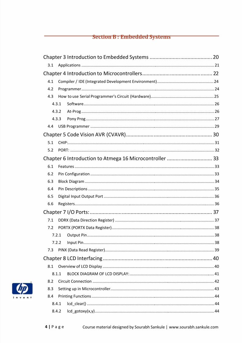
A color scheme is followed to give the specifications of a resistor. The table for color code isshown below:
The 1 st two bands specify the 2 digits of the resistor value whereas the3 rd band specifies the multiplier in terms of the power to which 10 israised and multiplied to the 2 digits.
The tolerance tells the possible % variation of the resistor value aboutthe value indicated by bands.
1.7.2 Capacitor:
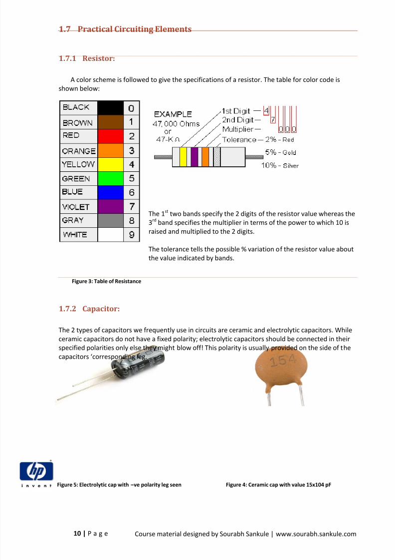
The 2 types of capacitors we frequently use in circuits are ceramic and electrolytic capacitors. Whileceramic capacitors do not have a fixed polarity; electrolytic capacitors should be connected in theirspecified polarities only else they might blow off! This polarity is usually provided on the side of thecapacitors ‘corresponding leg.
Figure 5: Electrolytic cap with –ve polarity leg seen Figure 4: Ceramic cap with value 15x104 pF
Figure 3: Table of Resistance
8/6/2019 Course Manual - 2010
http://slidepdf.com/reader/full/course-manual-2010 11/71
11 | P a g e Course material designed by Sourabh Sankule | www.sourabh.sankule.com
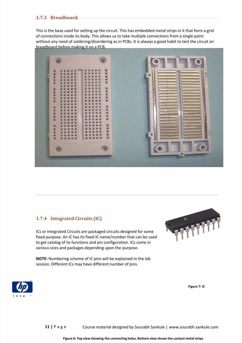
1.7.3 Breadboard:
This is the base used for setting up the circuit. This has embedded metal strips in it that form a gridof connections inside its body. This allows us to take multiple connections from a single pointwithout any need of soldering/disordering as in PCBs. It is always a good habit to test the circuit onbreadboard before making it on a PCB.
1.7.4 Integrated Circuits (IC)
ICs or Integrated Circuits are packaged circuits designed for somefixed purpose. An IC has its fixed IC name/number that can be usedto get catalog of its functions and pin configuration. ICs come invarious sizes and packages depending upon the purpose.
NOTE: Numbering scheme of IC pins will be explained in the labsession. Different ICs may have different number of pins.
Figure 6: Top view showing the connecting holes. Bottom view shows the contact metal strips
Figure 7: IC

8/6/2019 Course Manual - 2010
http://slidepdf.com/reader/full/course-manual-2010 12/71
12 | P a g e Course material designed by Sourabh Sankule | www.sourabh.sankule.com
1.7.5 LED
LED (Light Emitting Diode) is frequently used to display the outputs at various stages of the circuit. Itis essentially a Diode with the energy released in the form of photons due to electron transitionsfalling in the visible region. Hence normal diode properties apply to it.
It glows only in fwd bias mode i.e. with p junction connected to +ve voltage and n junction tonegative.
Diodes are essentially low power devices. The current through the LED should be less than20mA.Hence always put a 220 ohm resistor in series with the LED.
Never forget that LEDs consume a significant amount of power of the outputs of the ICs (CMOSbased).Hence it is advisable to only use them for checking the voltage level (high or low) and thenremove them.
Figure 8: LEDs

8/6/2019 Course Manual - 2010
http://slidepdf.com/reader/full/course-manual-2010 13/71
13 | P a g e Course material designed by Sourabh Sankule | www.sourabh.sankule.com
Chapter 2 Some Integrated Circuits and Implementation
2.1 555
555 is an IC used to generate a clock .Thetwo attributes of a clock are
Frequency Duty cycle.
Both of these can be changed using this IC,however the duty cycle is always <50%.
There are two modes in which 555 can run.
2.1.1 Monostable mode
As the name suggests; in this mode the output is stable in only one (mono) state i.e. ‘off’ state.Thus it can stay only for a finite time, if triggered, to the other state i.e. ‘on’ state. This time can beset choosing appropriate values of resistances in the formula:
T = 1.1 x R1 x C1
Figure 10: 555 in monostable mode
Figure 9: Pin Configuration of 555

8/6/2019 Course Manual - 2010
http://slidepdf.com/reader/full/course-manual-2010 14/71
14 | P a g e Course material designed by Sourabh Sankule | www.sourabh.sankule.com
2.1.2 Astable mode
In this mode; the output is stable neither in ‘high’ state nor in ‘low ’ state. Hence it oscillates fromone state to another giving us a square wave or clock. We can set the clock frequency and Duty cycleD by the formulae:
F = ( )
D =
Figure 11: 555 in astable mode
NOTE: Capacitor C2 is just to filter the noise and its value can be suitably chosen to be 0.01µF. It canalso be neglected.
8/6/2019 Course Manual - 2010
http://slidepdf.com/reader/full/course-manual-2010 15/71
15 | P a g e Course material designed by Sourabh Sankule | www.sourabh.sankule.com
2.2 4029 counter
With the clock made, we are ready to count the number of pulses passed into the circuit. Note thatany kind of counting requires a memory (you got to know that you have just counted ‘3’ to go to‘4’!). Hence 4029 can also be used as a memory element that remembers its immediate previousstate.
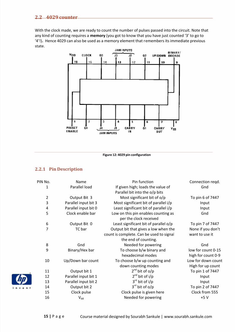
Figure 12: 4029 pin configuration
2.2.1 Pin Description
PIN No. Name Pin function Connection reqd.1 Parallel load If given high; loads the value of
Parallel bit into the o/p bitsGnd
2 Output Bit 3 Most significant bit of o/p To pin 6 of 74473 Parallel input bit 3 Most significant bit of parallel i/p Input4 Parallel input bit 0 Least significant bit of parallel i/p Input5 Clock enable bar Low on this pin enables counting as
per the clock receivedGnd
6 Output Bit 0 Least significant bit of parallel o/p To pin 7 of 74477 TC bar Output bit that gives a low when the
count is complete. Can be used to signalthe end of counting.
None if you don’twant to use it
8 Gnd Needed for powering Gnd9 Binary/Hex bar To choose b/w binary and
hexadecimal modeslow for count 0-15high for count 0-9
10 Up/Down bar count To choose b/w up counting anddown counting modes
Low for down countHigh for up count
11 Output bit 1 2 nd bit of o/p To pin 1 of 744712 Parallel input bit 1 2 nd bit of i/p Input13 Parallel input bit 2 3 rd bit of i/p Input14 Output bit 2 3 rd bit of o/p To pin 2 of 744715 Clock pulse Clock pulse is given here Clock from 55516 Vdd Needed for powering +5 V

8/6/2019 Course Manual - 2010
http://slidepdf.com/reader/full/course-manual-2010 16/71
16 | P a g e Course material designed by Sourabh Sankule | www.sourabh.sankule.com
2.3 7447: BCD to 7 segment display decoder
For displaying the number in the counter output on a seven segment display (i.e. 7 LEDsmaking up a figure of ‘8’ as in a general calculator. See fig. ) we need to decode the 4 bits andmatch them to the 7 pins for lighting the LEDs corresponding to the number. This work isdone by 7447.
Figure 13: 7447 pin configuration
2.3.1 Pin Description
PINno.
Name Function Connection reqd.
1 i/p B 2 nd bit(O1) of 4029’s o/p To O1 of 40292 i/p C 3rd bit(O2) of 4029’s o/p To O2 of 40293 Lamp Test
barUsed to check that all LEDs of 7 seg
are working.High for normal fn
Low to glow allLEDs
4 BI /RBI Kept high to allow normal function Kept high5 RBI Blanks ‘0’ from being displayed Kept high6 i/p D Most significant bit(O3) of 4029’s
o/pTo O2 of 4029
7 i/p A 3rd bit(O2) of 4029’s o/p To O2 of 40298 Gnd For power Connected to gnd
9-15 a-g as per thefig
The o/p pins to 7segment display To 7 seg display
16 Vcc For power Connected to +5 V
NOTE:
The COM pins are to be connected to Vcc via 220 ohm resistor. Why resistor is required??
The dot pin is just for display of decimal point and essentially only makes the upper andlower sides distinguishable from each other for a single display. without the asymmetryproduced by dot how will we be able to see which side is upper and which is lower?
8/6/2019 Course Manual - 2010
http://slidepdf.com/reader/full/course-manual-2010 17/71
17 | P a g e Course material designed by Sourabh Sankule | www.sourabh.sankule.com
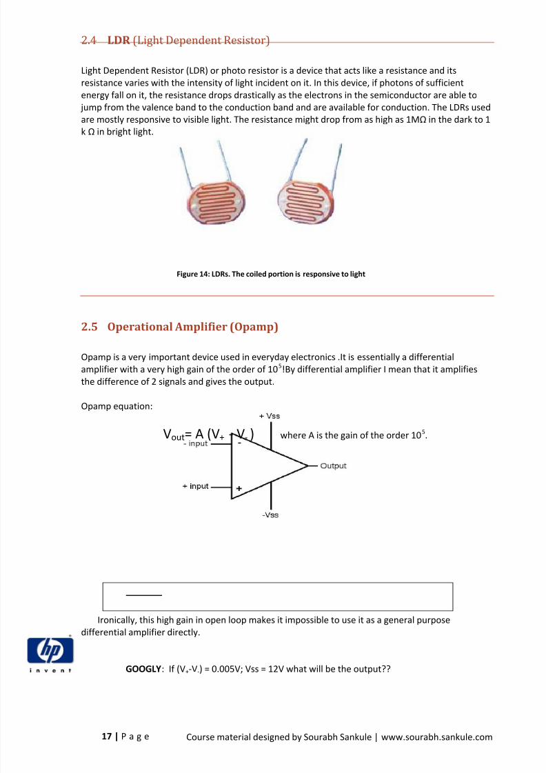
2.4 LDR (Light Dependent Resistor)
Light Dependent Resistor (LDR) or photo resistor is a device that acts like a resistance and itsresistance varies with the intensity of light incident on it. In this device, if photons of sufficientenergy fall on it, the resistance drops drastically as the electrons in the semiconductor are able to
jump from the valence band to the conduction band and are available for conduction. The LDRs usedare mostly responsive to visible light. The resistance might drop from as high as 1MΩ in the dark to 1
k Ω in bright light.
2.5 Operational Amplifier (Opamp)
Opamp is a very important device used in everyday electronics .It is essentially a differentialamplifier with a very high gain of the order of 10 5!By differential amplifier I mean that it amplifiesthe difference of 2 signals and gives the output.
Opamp equation:
Vout = A (V+ - V- ) where A is the gain of the order 10 5.
Ironically, this high gain in open loop makes it impossible to use it as a general purposedifferential amplifier directly.
Figure 14: LDRs. The coiled portion is responsive to light
GOOGLY: If (V+-V-) = 0.005V; Vss = 12V what will be the output??

8/6/2019 Course Manual - 2010
http://slidepdf.com/reader/full/course-manual-2010 18/71
18 | P a g e Course material designed by Sourabh Sankule | www.sourabh.sankule.com
2.5.1 Opamp as a comparator
Simplest use of Opamp is as a comparator. It can be used to convert an analog signal to a digitalsignal defined by a fixed threshold. Set V- as the threshold voltage say 2.5 V and apply the analogsignal to be digitized at V+ .What will be the output? Well if you have worked out the googly; thisshould be a piece of cake!
2.6 7805 Voltage Regulator
7805 voltage regulator is used to get +5 V output out of a higher voltage supply (7.5V-20V).We useadapter’s supply to generate +5V here. Connect the gnd and +12V of adapter to the p ins as shownand get +5V directly as an output out of the 3 rd pin. Current up to 0.5 A can be obtained from thisregulator without any significant fall in voltage level.
NOTE: Use 2 capacitors of value say 0.1µF to filter the noise in the input and output of regulator’ssupply as shown.

8/6/2019 Course Manual - 2010
http://slidepdf.com/reader/full/course-manual-2010 19/71
19 | P a g e Course material designed by Sourabh Sankule | www.sourabh.sankule.com
Section B
Embedded Systems

8/6/2019 Course Manual - 2010
http://slidepdf.com/reader/full/course-manual-2010 20/71
20 | P a g e Course material designed by Sourabh Sankule | www.sourabh.sankule.com
Chapter 3 Introduction to Embedded Systems
Embedded system is a scaled down computer system which is designed to perform a specifictask/operation. Unlike a general purpose computersystem which is used for a variety of tasks, like playingmusic, games, surfing internet etc. The term embeddedtells that whole system is embedded into an appliance. Asingle chip contains both hardware and software(technically, firmware). It is designed to performoperations which minimize (or even completely avoid)need of human control.
Basic Flow diagram for embedded computer systems can be shown as:
Some important things to note about embedded systems:
1. Once an embedded hardware is programmed for a certain task, it is used forever for thesame task. Changing the firmware afterwards is not possible.
2. Such systems are limited in computational resources like memory, CPU processing speed,I/O facilities but are still capable of performing the task given to them very efficiently.
3. Embedded systems can also be having a reduced functionality version of operating systemcalled RTOS (Real Time Operating System) for highly specialized applications.

8/6/2019 Course Manual - 2010
http://slidepdf.com/reader/full/course-manual-2010 21/71
21 | P a g e Course material designed by Sourabh Sankule | www.sourabh.sankule.com
3.1 Applications
An embedded system may be used for a variety of purposes. Some examples of an embeddedsystem are:
1. Security System2.
Mobile and PDA
3. Alarm system4. Automobile system5. Digital Camera6. Environment monitoring systems (using sensors and actuators)
Embedded systems are often required to perform real time operations. By Real time operations,we mean that, operations where delay of even a few milliseconds could be dangerous. Some realtime systems may be:
1. Sensor system in Nuclear Plants2. Flight control systems3. Automobile Braking system and engine controlling systems
These are situations where we need very accurate timing and control. Failure in such situationsmay cause great loss.

8/6/2019 Course Manual - 2010
http://slidepdf.com/reader/full/course-manual-2010 22/71
22 | P a g e Course material designed by Sourabh Sankule | www.sourabh.sankule.com
Chapter 4 Introduction to Microcontrollers
You must be knowing about Digital Integrated Circuits (ICs) right ? For example:
7404: Hex Inverter 7408: Quad 2-input AND gate 7410: Triple 3-input NAND Gate 7432: Quad 2-input OR Gate 7457: 60:1 Frequency divider
There are AND, XOR, NAND, NOR, OR logic gate ICs, Counters, Timers, Seven SegmentDisplay Drivers and much more. Just check out 7400 Series and 4000 Series of IntegratedCircuits.
Now let’s take Quad 2 input AND gate IC. It has 4 AND gates, each having 2 pins for inputand 1 pin for output. The truth table or the function table of each gate is fixed. This is asfollows,
Input 1 Input 2 Output
0 0 0
0 1 0
1 0 0
1 1 1
Similarly all the Integrated circuits have their function tables and input and output pins fixed.You cannot change the function and no input pin act as output and vice versa. So wheneveryou want to design some circuit you first have to get the output as a function of inputs andthen design it using gates or whatever the requirement is.
So once a circuit is built we cannot change its function ! Even if you want to make somechanges again you have to consider all the gates and components involved. Now if you aredesigning any circuit which involves change of the function table every now and then you arein trouble ! For example if I want to design an Autonomous Robot which should perform
various tasks and I don’t just want to fix the task. Suppose I make it to move in a path then Iwant to change the path ! How to do that ?
Here comes the use of Microcontrollers ! Now if I give you an Integrated Circuit with 20 pinsand tell you that you can make any pin as output or input also you can change the functionta ble by programming the IC using your computer ! Then your reactions will be wow ! that’snice :- ) That’s what the most basic function of a microcontroller is. It has set of pins called asPORT and you can make any pin either as output or input. After configuring pins you canprogram it to perform according to any function table you want. You can change theconfiguration or the function table as many times you wants.
There are many Semiconductor Companies which manufacturesmicrocontrollers. Some of them are:

8/6/2019 Course Manual - 2010
http://slidepdf.com/reader/full/course-manual-2010 23/71
23 | P a g e Course material designed by Sourabh Sankule | www.sourabh.sankule.com
Intel Atmel Microchip Motorola
We will discuss about Atmel Microcontrollers commonly known as AVR in this section.
Question: How a microcontroller works !
Answer: Well I cannot go into lot of details about the working because it is a vast topic initself. I can just give an overview.
Microcontroller consists of an Microprocessor (CPU that is Central processing Unit) which isinterfaced to RAM (Random Access Memory) and Flash Memory (one your pen drive has !).You feed your program in the Flash Memory on the microcontroller. Now when you turn onthe microcontroller, CPU accesses the instruction from RAM which access your code fromFlash. It sets the configuration of pins and start performing according to your program.
Question: How to make the code ?
Answer: You basically write the program on your computer in any of the high levellanguages like C, C++, JAVA etc. Then you compile the code to generate the machine file.Now you will ask what this machine file is ? All the machines understand only one language,0 & 1 that is on and off. Now this 0 & 1 both corresponds to 2 different voltage levels forexample 0 volt for 0 logic and +5 volt for 1 logic. Actually the code has to be written in this0, 1 language and then saved in the memory of the microcontroller. But this will be verydifficult for us ! So we write the code in the language we understand (C) and then compileand make the machine file (.hex). After we make this machine file we feed this to thememory of the microcontroller.
Question: How to feed the code in the flash of Microcontroller ?
Answer: Assuming you have the machine file (.hex) ready and now you want to feed that tothe flash of the microcontroller. Basically you want to make communication between yourcomputer and microcontroller. Now computer has many communication ports such as SerialPort , Parallel Port and USB (Universal Serial Bus) .
Lets take Serial Port, it has its own definition that is voltage level to define 0 & 1 (yeah allthe data communication is a just collection of 0 & 1 ) Serial Port's protocol is called as UART (Universal Asynchronous Receiver & Transmitter) Its voltage levels are :-12 volt for 0 logic
and +12 volt for 1 logic.
Now the voltage levels of our microcontroller are based on CMOS (Complementary MetalOxide Semiconductor) technology which has 0 volt for 0 logic and +5 volt for 1 logic.
Two different machines with 2 different ways to define 0 & 1 and we want to exchangeinformation between them. Consider microcontroller as a French and Computer's Serial Portas an Indian person (obviously no common language in between !) If they want to exchangeinformation they basically need a mediator who knows both the language. He will listen oneperson and then translate to other person. Similarly we need a circuit which converts CMOS(microcontroller) to UART (serial port) and vice versa. This circuit is called as programmer.Using this circuit we can connect computer to the microcontroller and feed the machine fileto the flash.
8/6/2019 Course Manual - 2010
http://slidepdf.com/reader/full/course-manual-2010 24/71
24 | P a g e Course material designed by Sourabh Sankule | www.sourabh.sankule.com
4.1 Compiler / IDE (Integrated Development Environment)
Atmel Microcontrollers are very famous as they are very easy to use. There are manydevelopment tools available for them. First of all we need an easy IDE for developing code. I
suggest beginners to use CVAVR (Code Vision AVR) Evaluation version is available for freedownload from the website. It has limitation of code size. It works on computers withWindows platform that is Windows XP & Vista.
Some famous compilers/development tools supporting Windows for Atmel Microcontrollersare:
WINAVR (AVRGCC for Windows) Code Vision AVR (CVAVR) AVR Studio (Atmel's free developing tool)
AVRGCC is a very nice open source compiler used by most of the people.
4.2 Programmer
Programmer basically consists of two parts:
Software (to open .hex file on your computer) Hardware (to connect microcontroller)
Hardware depends on the communication port you are using on the computer (Serial, Parallelor USB). I suggest beginners to use Serial Programmer as it is very easy to build. Softwarefor that is Pony Prog. Some famous Windows (XP, Vista) programmers are:
Pony Prog (Serial, Parallel) AVRdude (supports many hardwares) AVRStudio (supports Atmel's hardware) ATProg (Serial) USB-ASP(USB)

8/6/2019 Course Manual - 2010
http://slidepdf.com/reader/full/course-manual-2010 25/71
25 | P a g e Course material designed by Sourabh Sankule | www.sourabh.sankule.com
4.3 How to use Serial Programmer's Circuit (Hardware)
This is the easiest programmer circuit to make. You just have to get Serial Port connector andthree 1K resistors and you are done! Circuit Diagram is attached.
Now open the datasheet of Atmega you are using (I am using Atmega-16). Go to the pin
configuration and find the following pins and connect the programmer. Programming is donethrough SPI (Serial Peripheral Interface) which involves MISO, MOSI and SCK pins. RESET is used toreset the chip. 0 volt on this pin will reset the chip and for normal running it should be pulled up to+5V.
MOSI (Master Out Slave In) MISO (Master In Slave Out) SCK (Serial Clock) RESET GND (Ground)
Now connect the power supplies that are Vcc andGND to the micro controller.
Vcc = +5V and GND = 0V
Do not forget to connect Reset to Vcc with a 1K/10K resistor for pulling up.
That is it we are ready with the hardware.
Note: - The Trainer Board has On-Board Serial Programmer.
8/6/2019 Course Manual - 2010
http://slidepdf.com/reader/full/course-manual-2010 26/71
26 | P a g e Course material designed by Sourabh Sankule | www.sourabh.sankule.com
4.3.1 Software
As I told you there are two parts of a programmer, hardware and software. We can build thishardware as it is very easy with just 3-4 components. Now we need software which support thishardware and can comminucate with micro controller using this circuit. There are 2 good softwaresfor Windows. They are,
Pony Prog At-Prog
Both of them support Serial as well as Parallel port, but I have always preferred serial portbecause it has only 9 pins, hence a smaller connector is required.
Now let us discuss about them.
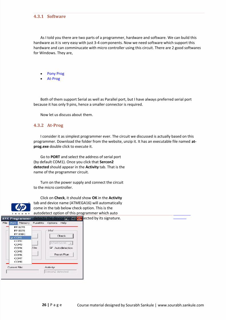
4.3.2 At-Prog
I consider it as simplest programmer ever. The circuit we discussed is actually based on thisprogrammer. Download the folder from the website, unzip it. It has an executable file named at-prog.exe double click to execute it.
Go to PORT and select the address of serial port(by default COM1). Once you click that Sercon2
detected should appear in the Activity tab. That is thename of the programmer circuit.
Turn on the power supply and connect the circuitto the micro controller.
Click on Check , it should show OK in the Activity tab and device name (ATMEGA16) will automaticallycome in the tab below check option. This is theautodetect option of this programmer which autodetects the device name connected by its signature.

8/6/2019 Course Manual - 2010
http://slidepdf.com/reader/full/course-manual-2010 27/71
27 | P a g e Course material designed by Sourabh Sankule | www.sourabh.sankule.com
Now just open the device file from File--->Open and click on Write . It will write andverify the program. Done! So simple isn’t it?:)
4.3.3 Pony Prog
One of the most commonly used programmers on Windows. Download it from the website andinstall it. Now let’s set it up for our hardware.
First select AVR micro and AVR-Auto (you can also specify device name, Atmega16 ) in the chipoptions (last two drop down tabs)
Go to the Setup ---->Interface-Setup . Then do the settings as shown in the picture below. Thenconnect the circuit to the microcontroller, turn on the power supply. Now click on Probe . You shouldget Test OK message. If not, check your connections again.

8/6/2019 Course Manual - 2010
http://slidepdf.com/reader/full/course-manual-2010 28/71
28 | P a g e Course material designed by Sourabh Sankule | www.sourabh.sankule.com
Now let’s read the Microcontroller. Go to Command ---->Read All . It should start reading thesignature and the flash memory. You should get Read Successful message after that.
So we are done with the settings and testing’s. Everything i s working fine :) Now just open thehex file from File---->Open-Device-File

8/6/2019 Course Manual - 2010
http://slidepdf.com/reader/full/course-manual-2010 29/71
29 | P a g e Course material designed by Sourabh Sankule | www.sourabh.sankule.com
Go to Command ---->Write-Program (Flash) . It will start writing and then verifying the code.Congratulations :) you did it!
4.4 USB Programmer
USBasp is a USB in-circuit programmer for Atmel AVR controllers. It simply consists of anATMega48 or an ATMega8 and a couple of passive components. The programmer uses a firmware-only USB driver; no special USB controller is needed.
8/6/2019 Course Manual - 2010
http://slidepdf.com/reader/full/course-manual-2010 30/71
30 | P a g e Course material designed by Sourabh Sankule | www.sourabh.sankule.com
Chapter 5 Code Vision AVR (CVAVR)
An IDE has following functions:
Preprocessing Compilation Assembly Linking Object Translation Text Editor
If we just use compiler and linker independently we still need to get a text editor. Socombining everything will actually mess things up. So the best way is to get Software whichhas it all. That’s called an Integrated Development Environment, in short IDE.
I consider Code-Vision-AVR to be the best IDE for getting started with AVRprogramming on Windows XP, Vista. It has a very good Code Wizard which generate codesautomatically ! You need not mess with the assembly words. So in all my tutorials I will beusing CVAVR. You can download evaluation version for free which has code size limitationbut good enough for our purpose.
For all my examples I will be using Atmega-16 as default microcontroller because it veryeasily available and is powerful enough with sufficient number of pins and peripherals weuse. You can have a look on the datasheet of Atmega-16 in the datasheet section.
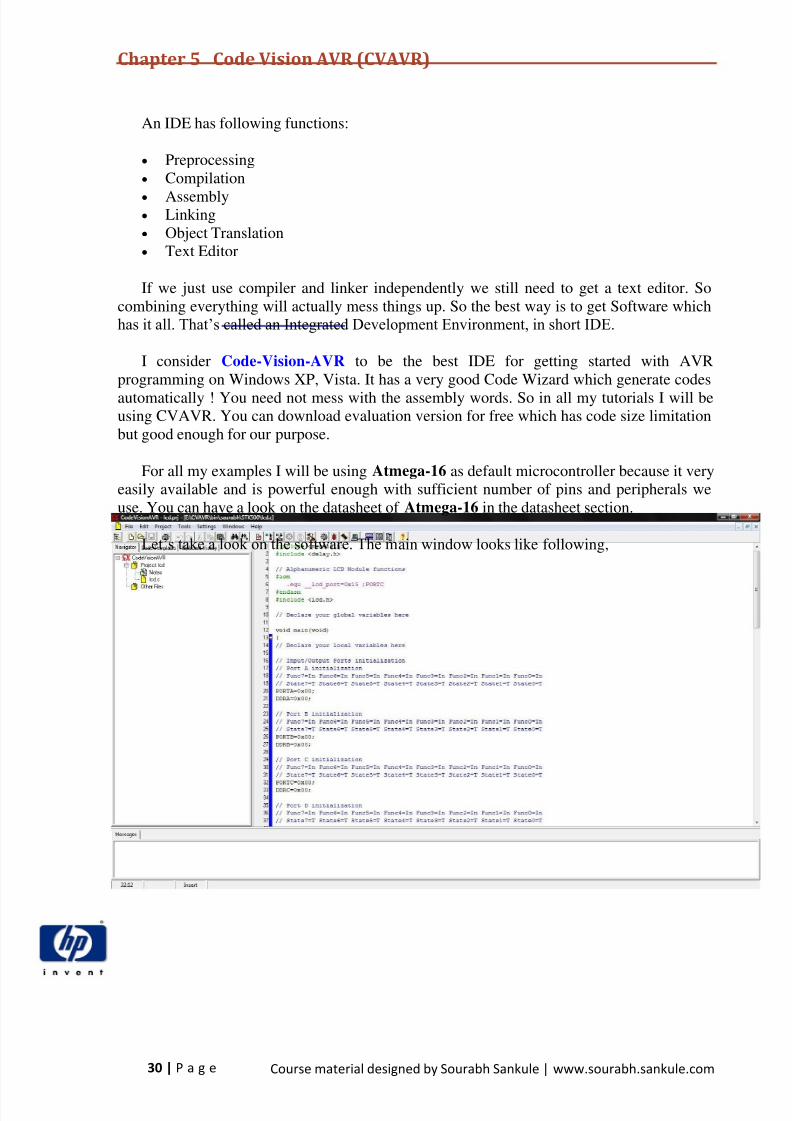
Let’s take a look on the software. The m ain window looks like following,

8/6/2019 Course Manual - 2010
http://slidepdf.com/reader/full/course-manual-2010 31/71
31 | P a g e Course material designed by Sourabh Sankule | www.sourabh.sankule.com
Now click on File ---> New --->Project
A pop up window will come asking whether you want to use Code Wizard AVR,obviously select yes because that is the reason we are using CVAVR !
Now have a look on this Wizard. It has many tabs where we can configure PORTS,TIMERS, LCD, ADC etc. I am explaining some of them
5.1 CHIP:
Select the chip for which you are going to write the program. Then select the frequency atwhich Chip is running. By default all chips are set on Internal Oscillator of 1 MHz so select 1MHz if that is the case. If you want to change the running clock frequency of the chip thenyou have to change its fuse bits (I will talk more about this in fuse bits section).
8/6/2019 Course Manual - 2010
http://slidepdf.com/reader/full/course-manual-2010 32/71
32 | P a g e Course material designed by Sourabh Sankule | www.sourabh.sankule.com
5.2 PORT:
PORT is usually a collection of 8 pins.
From this tab you can select which pin you want to configure as output and which asinput. It basically writes the DDR and PORT register through this setting. Registers arebasically RAM locations which configure various peripherals of microcontroller and by
changing value of these registers we can change the function it is performing. I will talk moreabout registers later. All the details are provided in the datasheet.
So you can configure any pin as output or input by clicking the box.
For Atmega-16 which has 4 Ports we can see 4 tabs each corresponding to one Port. Youcan also set initial value of the Pins you want to assign. or if you are using a pin as input thenwhether you want to make it as pull-up or tristated, again I will talk in details about thesefunctions later.
Similarly using this code wizard you can very easily configure all the peripherals on the
Atmega.
Now for generating code just go to File ----> Generate, Save and Exit (of the codewizard)
Now it will ask you name and location for saving three files. Two being project files andone being the .C file which is your program. try to keep same names of all three files to avoidconfusion. By default these files are generated in C:\CVAVR\bin
The generated program will open in the text editor. Have a look it has some declarationslike PORT, DDR, TCCR0 and many more. These are all registers which configures variousfunctions of Atmega and by changing these value we make different functions. All the detailsabout the registers are commented just below them. Now go down and find following infinitewhile loop there. We can start writing our part of program just before the while loop. And asfor most of the applications we want microcontroller to perform the same task forever we putour part of code in the infinite while loop provided by the code wizard !
while (1)
// Place your code here
;
See how friendly this code wizard is, all the work (configuring registers) automaticallydone and we don’t even need to understand and go to the details about registers too !
Now we want to generate the hex file, so first compile the program. Either press F9 or goto Project ---> Compile .
It will show compilation errors if any. If program is error free we can proceed to makingof hex file. So either press Shift+F9 or go to Project ----> Make . A pop up window will
come with information about code size and flash usage etc.
So the machine file is ready now ! It is in the same folder where we saved those 3 files.
8/6/2019 Course Manual - 2010
http://slidepdf.com/reader/full/course-manual-2010 33/71
33 | P a g e Course material designed by Sourabh Sankule | www.sourabh.sankule.com
Chapter 6 Introduction to Atmega 16 Microcontroller
6.1 Features
Advanced RISC Architecture Up to 16 MIPS Throughput at 16 MHz 16K Bytes of In-System Self-Programmable Flash 512 Bytes EEPROM 1K Byte Internal SRAM 32 Programmable I/O Lines In-System Programming by On-chip Boot Program 8-channel, 10-bit ADC Two 8-bit Timer/Counters with Separate Prescalers and Compare Modes One 16-bit Timer/Counter with Separate Prescaler, Compare Mode, and Capture Four PWM Channels
Programmable Serial USART Master/Slave SPI Serial Interface Byte-oriented Two-wire Serial Interface Programmable Watchdog Timer with Separate On-chip Oscillator External and Internal Interrupt Sources
6.2 Pin Configuration

8/6/2019 Course Manual - 2010
http://slidepdf.com/reader/full/course-manual-2010 34/71
34 | P a g e Course material designed by Sourabh Sankule | www.sourabh.sankule.com
6.3 Block Diagram

8/6/2019 Course Manual - 2010
http://slidepdf.com/reader/full/course-manual-2010 35/71
35 | P a g e Course material designed by Sourabh Sankule | www.sourabh.sankule.com
6.4 Pin Descriptions
VCC: Digital supply voltage. (+5V)
GND: Ground. (0 V) Note there are 2 ground Pins.
Port A (PA7 - PA0)Port A serves as the analog inputs to the A/D Converter. Port A also serves as an 8-bit bi-directional I/O port, if the A/D Converter is not used. When pins PA0 to PA7 are used as inputs andare externally pulled low, they will source current if the internal pull-up resistors are activated. ThePort A pins are tri-stated when a reset condition becomes active, even if the clock is not running.
Port B (PB7 - PB0)Port B is an 8-bit bi-directional I/O port with internal pull-up resistors (selected for each bit). Port
B also serves the functions of various special features of the ATmega16 as listed on page 58 of datasheet.
Port C (PC7 - PC0)Port C is an 8-bit bi-directional I/O port with internal pull-up resistors (selected for each bit). Port
C also serves the functions of the JTAG interface and other special features of the ATmega16 aslisted on page 61 of datasheet. If the JTAG interface is enabled, the pull-up resistors on pinsPC5(TDI), PC3(TMS) and PC2(TCK) will be activated even if a reset occurs.
Port D (PD7 - PD0)Port D is an 8-bit bi-directional I/O port with internal pull-up resistors (selected for each bit).
Port D also serves the functions of various special features of the ATmega16 as listed on page 63 of datasheet.
RESET: Reset Input. A low level on this pin for longer than the minimum pulse length willgenerate a reset, even if the clock is not running.
XTAL1: External oscillator pin 1
XTAL2: External oscillator pin 2
AVCC: AVCC is the supply voltage pin for Port A and the A/D Converter. It should be externallyconnected to V CC, even if the ADC is not used. If the ADC is used, it should be connected to V CC
through a low-pass filter.
AREF: AREF is the analog reference pin for the A/D Converter.

8/6/2019 Course Manual - 2010
http://slidepdf.com/reader/full/course-manual-2010 36/71
36 | P a g e Course material designed by Sourabh Sankule | www.sourabh.sankule.com
6.5 Digital Input Output Port
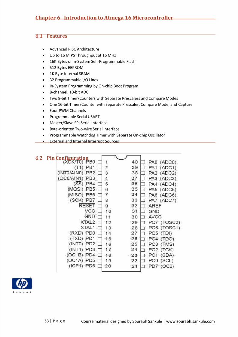
So let’s start with understanding the functioning of AVR. We will first discuss about I/OPorts. Again I remind you that I will be using and writing about Atmega-16 . Let’s first havea look at the Pin configuration of Atmega-16. Image is attached, click to enlarge.
You can see it has 32 I/O (Input/Output) pins grouped as A, B, C & D with 8 pins in eachgroup. This group is called as PORT.
PA0 - PA7 (PORTA) PB0 - PB7 (PORTB) PC0 - PC7 (PORTC) PD0 - PD7 (PORTD)
Notice that all these pins have some function written in bracket. These are additional functionthat pin can perform other than I/O. Some of them are.
ADC (ADC0 - ADC7 on PORTA) UART (Rx,Tx on PORTD) TIMERS (OC0 - OC2) SPI (MISO, MOSI, SCK on PORTB) External Interrupts (INT0 - INT2)
6.6 Registers
All the configurations in microcontroller is set through 8 bit (1 byte) locations in RAM(RAM is a bank of memory bytes) of the microcontroller called as Registers . All thefunctions are mapped to its locations in RAM and the value we set at that location that is atthat Register configures the functioning of microcontroller. There are total 32 x 8bit registersin Atmega-16. As Register size of this microcontroller is 8 bit, it called as 8 bitmicrocontroller.

8/6/2019 Course Manual - 2010
http://slidepdf.com/reader/full/course-manual-2010 37/71
37 | P a g e Course material designed by Sourabh Sankule | www.sourabh.sankule.com
Chapter 7 I/O Ports:
Input Output functions are set by Three Registers for each PORT.
DDRX ----> Sets whether a pin is Input or Output of PORTX. PORTX ---> Sets the Output Value of PORTX.
PINX -----> Reads the Value of PORTX.
Go to the page 50 in the datasheet or you can also see the I/O Ports tab in the Bookmarks.
7.1 DDRX (Data Direction Register)
First of all we need to set whether we want a pin to act as output or input. DDRX register sets
this. Every bit corresponds to one pin of PORTX. Let’s have a look on DDRA register.
Bit 7 6 5 4 3 2 1 0
PIN PA7 PA6 PA5 PA4 PA3 PA2 PA1 PA0
Now to make a pin act as I/O we set its corresponding bit in its DDR register.
To make Input set bit 0 To make Output set bit 1
If I write DDRA = 0xFF (0x for Hexadecimal number system) that is setting all the bits of DDRA to be 1, will make all the pins of PORTA as Output.
Similarly by writing DDRD = 0x00 that is setting all the bits of DDRD to be 0, will make allthe pins of PORTD as Input.
Now let’s take another example. Consider I want to set the pins of PORTB as shown in table,
PORT-B PB7 PB6 PB5 PB4 PB3 PB2 PB1 PB0
Function Output Output Input Output Input Input Input Output
DDRB 1 1 0 1 0 0 0 1
For this configuration we have to set DDRB as 11010001 which in hexadecimal is D1 . So wewill write DDRB=0xD1
Summary
DDRX -----> to set PORTX as input/output with a byte. DDRX.y ---> to set yth pin of PORTX as input/output with a bit (works only with CVAVR).
8/6/2019 Course Manual - 2010
http://slidepdf.com/reader/full/course-manual-2010 38/71
38 | P a g e Course material designed by Sourabh Sankule | www.sourabh.sankule.com
7.2 PORTX (PORTX Data Register)
This register sets the value to the corresponding PORT. Now a pin can be Output or Input. Solet’s discuss both the cases.
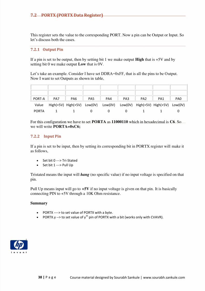
7.2.1 Output Pin
If a pin is set to be output, then by setting bit 1 we make output High that is +5V and bysetting bit 0 we make output Low that is 0V.
Let’s take an example. Consider I have set DDRA=0xFF, that is all the pins to be O utput.Now I want to set Outputs as shown in table,
PORT-A PA7 PA6 PA5 PA4 PA3 PA2 PA1 PA0
Value High(+5V) High(+5V) Low(0V) Low(0V) Low(0V) High(+5V) High(+5V) Low(0V)
PORTA 1 1 0 0 0 1 1 0
For this configuration we have to set PORTA as 11000110 which in hexadecimal is C6 . Sowe will write PORTA=0xC6;
7.2.2 Input Pin
If a pin is set to be input, then by setting its corresponding bit in PORTX register will make it
as follows, Set bit 0 ---> Tri-Stated Set bit 1 ---> Pull Up
Tristated means the input will hang (no specific value) if no input voltage is specified on thatpin.
Pull Up means input will go to +5V if no input voltage is given on that pin. It is basicallyconnecting PIN to +5V through a 10K Ohm resistance.
Summary
PORTX ----> to set value of PORTX with a byte. PORTX.y --> to set value of y th pin of PORTX with a bit (works only with CVAVR).

8/6/2019 Course Manual - 2010
http://slidepdf.com/reader/full/course-manual-2010 39/71
39 | P a g e Course material designed by Sourabh Sankule | www.sourabh.sankule.com
7.3 PINX (Data Read Register)
This register is used to read the value of a PORT. If a pin is set as input then correspondingbit on PIN register is,
0 for Low Input that is V < 2.5V 1 for High Input that is V > 2.5V (Ideally, but actually 0.8 V - 2.8 V is error zone !)
For an example consider I have connected a sensor on PC4 and configured it as an input pinthrough DDR register. Now I want to read the value of PC4 whether it is Low or High. So Iwill just check 4th bit of PINC register.
We can only read bits of the PINX register; can never write on that as it is meant for readingthe value of PORT.
Summary
PINX ----> Read complete value of PORTX as a byte. PINX.y --> Read y th pin of PORTX as a bit (works only with CVAVR).
I hope you must have got basic idea about the functioning of I/O Ports. For detailed readingyou can always refer to datasheet of Atmega .
8/6/2019 Course Manual - 2010
http://slidepdf.com/reader/full/course-manual-2010 40/71
40 | P a g e Course material designed by Sourabh Sankule | www.sourabh.sankule.com
Chapter 8 LCD Interfacing
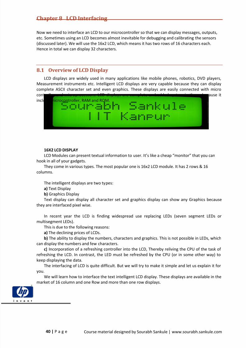
Now we need to interface an LCD to our microcontroller so that we can display messages, outputs,etc. Sometimes using an LCD becomes almost inevitable for debugging and calibrating the sensors(discussed later). We will use the 16x2 LCD, which means it has two rows of 16 characters each.Hence in total we can display 32 characters.
8.1 Overview of LCD DisplayLCD displays are widely used in many applications like mobile phones, robotics, DVD players,
Measurement instruments etc. Intelligent LCD displays are very capable because they can displaycomplete ASCII character set and even graphics. These displays are easily connected with microcontroller and microprocessors. LCD displays are complete embedded system in them, because itinclude microcontroller, RAM and ROM.
16X2 LCD DISPLAYLCD Modules can present textual information to user. I t’s like a cheap “monitor” that you can
hook in all of your gadgets.They come in various types. The most popular one is 16x2 LCD module. It has 2 rows & 16
columns.
The intelligent displays are two types:a) Text Displayb) Graphics DisplayText display can display all character set and graphics display can show any Graphics because
they are interfaced pixel wise.
In recent year the LCD is finding widespread use replacing LEDs (seven segment LEDs ormultisegment LEDs).
This is due to the following reasons:a) The declining prices of LCDs.b) The ability to display the numbers, characters and graphics. This is not possible in LEDs, which
can display the numbers and few characters.c) Incorporation of a refreshing controller into the LCD, Thereby reliving the CPU of the task of
refreshing the LCD. In contrast, the LED must be refreshed by the CPU (or in some other way) tokeep displaying the data.
The interfacing of LCD is quite difficult. But we will try to make it simple and let us explain it foryou.
We will learn how to interface the text intelligent LCD display. These displays are available in themarket of 16 column and one Row and more than one row displays.
8/6/2019 Course Manual - 2010
http://slidepdf.com/reader/full/course-manual-2010 41/71
41 | P a g e Course material designed by Sourabh Sankule | www.sourabh.sankule.com
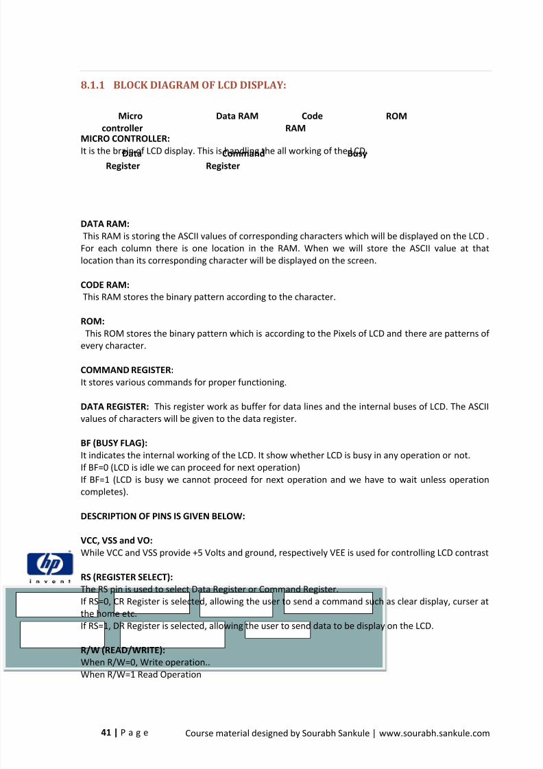
8.1.1 BLOCK DIAGRAM OF LCD DISPLAY:
MICRO CONTROLLER: It is the brain of LCD display. This is handling the all working of the LCD.
DATA RAM:This RAM is storing the ASCII values of corresponding characters which will be displayed on the LCD .
For each column there is one location in the RAM. When we will store the ASCII value at thatlocation than its corresponding character will be displayed on the screen.
CODE RAM: This RAM stores the binary pattern according to the character.
ROM:This ROM stores the binary pattern which is according to the Pixels of LCD and there are patterns of
every character.
COMMAND REGISTER:It stores various commands for proper functioning.
DATA REGISTER: This register work as buffer for data lines and the internal buses of LCD. The ASCIIvalues of characters will be given to the data register.
BF (BUSY FLAG): It indicates the internal working of the LCD. It show whether LCD is busy in any operation or not.If BF=0 (LCD is idle we can proceed for next operation)If BF=1 (LCD is busy we cannot proceed for next operation and we have to wait unless operationcompletes).
DESCRIPTION OF PINS IS GIVEN BELOW:
VCC, VSS and VO:While VCC and VSS provide +5 Volts and ground, respectively VEE is used for controlling LCD contrast
RS (REGISTER SELECT):The RS pin is used to select Data Register or Command Register.If RS=0, CR Register is selected, allowing the user to send a command such as clear display, curser atthe home etc.If RS=1, DR Register is selected, allowing the user to send data to be display on the LCD.
R/W (READ/WRITE):When R/W=0, Write operation..
When R/W=1 Read Operation
DataRegister
CommandRegister
Busy
CodeRAM
Data RAM
Microcontroller
ROM

8/6/2019 Course Manual - 2010
http://slidepdf.com/reader/full/course-manual-2010 42/71
42 | P a g e Course material designed by Sourabh Sankule | www.sourabh.sankule.com
EN (ENABLE):
The Enable pin is used by the LCD to latch binary bits available on its data pins. When data issupplied to data pins, a negative edge is applied to this pin So that the LCD latches in the datapresent at the data pins. This pulse must be a minimum of 450 ns wide.There should be positive edge at EN pin when read operation is required.
D7-D0:This is 8-bit data pins. D7-D0 are used to send information to the LCD or read the contents of theLCD’s internal registers.
BK-LED (LEDA, LEDK):These pins are used to give the supply to the back light of the LCD display. So, that content of theLCD display can be viewed in the dark.
8.2 Circuit Connection
There are 16 pins in an LCD; See reverse side of the LCD for the PIN configuration.The connections have to be made as shown below:
Figure 15: LCD connections

8/6/2019 Course Manual - 2010
http://slidepdf.com/reader/full/course-manual-2010 43/71
43 | P a g e Course material designed by Sourabh Sankule | www.sourabh.sankule.com
8.3 Setting up in Microcontroller
When we connect an LCD to Atmega16, one full PORT is dedicated to it, denoted by PORT-X inthe figure. To enable LCD interfacing in the microcontroller, just click on the LCD tab in the CodeWizard and select the PORT at which you want to connect the LCD. We will select PORTC. Also selectthe number of characters per line in your LCD. This is 16 in our case. Code Wizard now shows youthe complete list of connections which you will have to make in order to interface the LCD. These arenothing but the same as in the above figure for general PORT-X.
Figure 16: LCD settings on CVAVR wizard window.
As you can see, there are some special connections other than those to uC, Vcc and gnd. Theseare general LCD settings. Pin 3 (VO) is for the LCD contrast, ground it through a <1kΩ resistance/potentiometer for optimum contrast. Pin 15 & 16 (LEDA and LEDK) are for LCD backlight, give thempermanent +5V and GND respectively as we need to glow it continuously.

8/6/2019 Course Manual - 2010
http://slidepdf.com/reader/full/course-manual-2010 44/71
44 | P a g e Course material designed by Sourabh Sankule | www.sourabh.sankule.com
8.4 Printing Functions
Now once the connections have been made, we are ready to display something on our screen.Displaying our name would be great to start with. Some of the general LCD functions which you mustknow are:
8.4.1 lcd_clear()
Clears the lcd. Remember! Call this function before the while(1) loop, otherwise you won’t beable to see anything!
8.4.2 lcd_gotoxy(x,y)
Place the cursor at coordinates (x,y) and start writing from there. The first coordinate is (0,0).Hence, x ranges from 0 to 15 and y from 0 to 1 in our LCD. Suppose you want to display somethingstarting from the 5 th character in second line, then the function would be
lcd_gotoxy(5,1);
8.4.3 lcd_putchar(char c)
To display a single character. E.g.,lcd_putchar(‘H’);
8.4.4 lcd_putsf(constant string)
To display a constant string. Eg,
lcd_putsf(“ IIT Kanpur ”);
8.4.5 lcd_puts(char arr)
To display a variable string, which is nothing but an array of characters (data type char) in Clanguage . e.g., You have an array char c[10] which keeps on changing. Then to display it, thefunction would be called as
lcd_puts(c);
Now we have seen that only characters or strings (constant or variable) can be displayed on theLCD. But quite often we have to display values of numeric variables, which is not possible directly.Hence we need to first convert that numeric value to a string and then display it. For e.g., if we havea variable of type integer, say int k, and we need to display the value of k (which changes every nowand then, 200 now and 250 after a second... and so on). For this, we use the C functions itoa() andftoa() , but remember to include the header file stdlib.h to use these C functions.
8.4.6 itoa(int val, char arr[])
It stores the value of integer val in the character array arr. E.g., we have already defined int i andchar c[20], then
8/6/2019 Course Manual - 2010
http://slidepdf.com/reader/full/course-manual-2010 45/71
45 | P a g e Course material designed by Sourabh Sankule | www.sourabh.sankule.com
itoa(i,c);lcd_puts(c);
Similarly we have
8.4.7 ftoa(float val, char decimal_places, char arr[])
It stores the value of floating variable f in the character array arr with the number of decimal placesas specified by second parameter. E.g., we have already defined float f and char c[20], then
ftoa(f,4,c); // till 4 decimal placeslcd_puts(c);
Now we are ready to display anything we want on our LCD. Just try out something which youwould like to see glowing on it!

8/6/2019 Course Manual - 2010
http://slidepdf.com/reader/full/course-manual-2010 46/71
46 | P a g e Course material designed by Sourabh Sankule | www.sourabh.sankule.com
Chapter 9 UART Communication
UART (Universal Asynchronous Receiver Transmitter) is a way of communication between themicrocontroller and the computer system or another microcontroller. There are always two parts toany mode of communication-a Receiver and a Transmitter. Hence, our Atmega can receive data aswell as send data to other microcontroller, computer or any other device.
9.1 UART: Theory of Operation
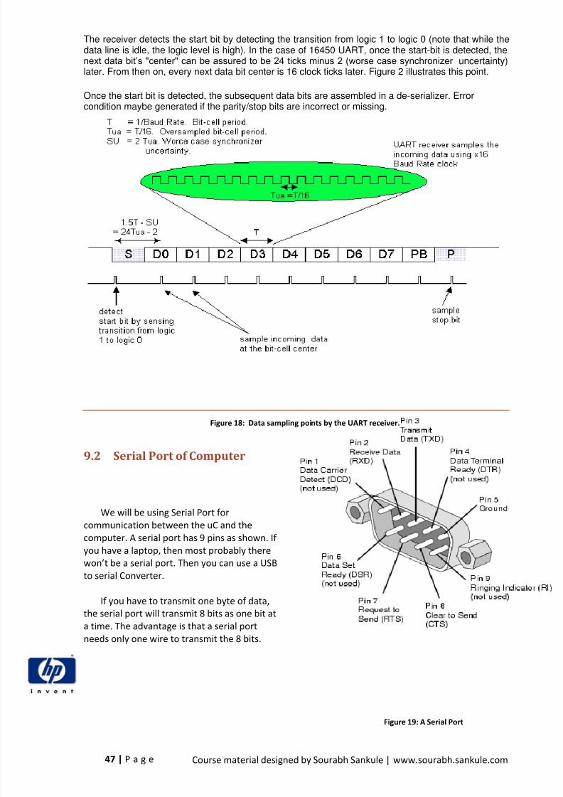
Figure 16 illustrates a basic UART data packet. While no data is being transmitted, logic 1 must beplaced in the Tx line. A data packet is composed of 1 start bit, which is always a logic 0, followed by aprogrammable number of data bits (typically between 6 to 8), an optional parity bit, and aprogrammable number of stop bits (typically 1). The stop bit must always be logic 1.
Most UART uses 8bits for data, no parity and 1 stop bit. Thus, it takes 10 bits to transmit a byte ofdata.
Figure 17: Basic UART packet format: 1 start bit, 8 data bits, 1 parity bit, 1 stop bit.
BAUD Rate: This parameter specifies the desired baud rate (bits per second) of the UART. Mosttypical standard baud rates are: 300, 1200, 2400, 9600, 19200, etc. However, any baud rate can beused. This parameter affects both the receiver and the transmitter. The default is 2400 (bauds).
In the UART protocol, the transmitter and the receiver do not share a clock signal. That is, a clocksignal does not emanate from one UART transmitter to the other UART receiver. Due to this reasonthe protocol is said to be asynchronous .
Since no common clock is shared, a known data transfer rate (baud rate) must be agreed upon priorto data transmission. That is, the receiving UART needs to know the transmitting UART’s baud rate(and conversely the transmitter needs to know the receiver’s baud rate, if a ny). In almost all cases thereceiving and transmitting baud rates are the same. The transmitter shifts out the data starting withthe LSB first.
Once the baud rate has been established (prior to initial communication), both the transmitter and thereceive r’s internal clock is set to the same frequency (though not the same phase). The receiver "synchronizes" its internal clock to that of the transmitter’s at the beginning of every data packetreceived. This allows the receiver to sample the data bit at the bit-cell center.
A key concept in UART design is that UART’s internal clock runs at much faster rate than the baudrate. For example, the popular 16450 UART controller runs its internal clock at 16 times the baud rate.This allows the UART receiver to sample the incoming data with granularity of 1/16 the baud-rateperiod. This "oversampling" is critical since the receiver adds about 2 clock-ticks in the input datasynchronizer uncertainty. The incoming data is not sampled directly by the receiver, but goes througha synchronizer which translates the clock domain from the transmitter’s to that of the receiver.
Additionally, the greater the granularity, the receiver has greater immunity with the baud rate error.
8/6/2019 Course Manual - 2010
http://slidepdf.com/reader/full/course-manual-2010 47/71
47 | P a g e Course material designed by Sourabh Sankule | www.sourabh.sankule.com
The receiver detects the start bit by detecting the transition from logic 1 to logic 0 (note that while thedata line is idle, the logic level is high). In the case of 16450 UART, once the start-bit is detected, thenext data bit’s "center" can be assured to be 24 ticks minus 2 (worse case synchronizer uncertainty)later. From then on, every next data bit center is 16 clock ticks later. Figure 2 illustrates this point.
Once the start bit is detected, the subsequent data bits are assembled in a de-serializer. Errorcondition maybe generated if the parity/stop bits are incorrect or missing.
9.2 Serial Port of Computer
We will be using Serial Port forcommunication between the uC and thecomputer. A serial port has 9 pins as shown. If you have a laptop, then most probably therewon’t be a serial port. Then you can use a USBto serial Converter.
If you have to transmit one byte of data,the serial port will transmit 8 bits as one bit ata time. The advantage is that a serial portneeds only one wire to transmit the 8 bits.
Figure 19: A Serial Port
Figure 18: Data sampling points by the UART receiver.
8/6/2019 Course Manual - 2010
http://slidepdf.com/reader/full/course-manual-2010 48/71
48 | P a g e Course material designed by Sourabh Sankule | www.sourabh.sankule.com
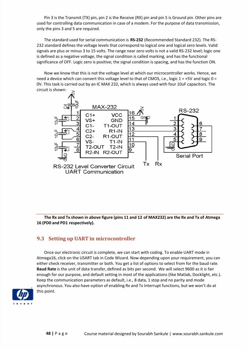
Pin 3 is the Transmit (TX) pin, pin 2 is the Receive (RX) pin and pin 5 is Ground pin. Other pins areused for controlling data communication in case of a modem. For the purpose of data transmission,only the pins 3 and 5 are required.
The standard used for serial communication is RS-232 (Recommended Standard 232). The RS-232 standard defines the voltage levels that correspond to logical one and logical zero levels. Validsignals are plus or minus 3 to 15 volts. The range near zero volts is not a valid RS-232 level; logic oneis defined as a negative voltage, the signal condition is called marking, and has the functional
significance of OFF. Logic zero is positive; the signal condition is spacing, and has the function ON.
Now we know that this is not the voltage level at which our microcontroller works. Hence, weneed a device which can convert this voltage level to that of CMOS, i.e., logic 1 = +5V and logic 0 =0V. This task is carried out by an IC MAX 232, which is always used with four 10uF capacitors. Thecircuit is shown:
The Rx and Tx shown in above figure (pins 11 and 12 of MAX232) are the Rx and Tx of Atmega16 (PD0 and PD1 respectively).
9.3 Setting up UART in microcontroller
Once our electronic circuit is complete, we can start with coding. To enable UART mode inAtmega16, click on the USART tab in Code Wizard. Now depending upon your requirement, you caneither check receiver, transmitter or both. You get a list of options to select from for the baud rate.Baud Rate is the unit of data transfer, defined as bits per second. We will select 9600 as it is fairenough for our purpose, and default setting in most of the applications (like Matlab, Docklight, etc.).Keep the communication parameters as default, i.e., 8 data, 1 stop and no parity and modeasynchronous. You also have o ption of enabling Rx and Tx Interrupt functions, but we won’t do atthis point.

8/6/2019 Course Manual - 2010
http://slidepdf.com/reader/full/course-manual-2010 49/71
49 | P a g e Course material designed by Sourabh Sankule | www.sourabh.sankule.com
Once you generate and save the code, all the register values are set by CVAVR and you only needto know some of the C functions to transfer data. Some of them are:
9.3.1 putchar()
To send one character to the buffer, which will be received by the device (uC or computer)? E.g.,
putchar(‘A’); //sends character ‘A’ to the buffer putchar(c); // sends a variable character c
9.3.2 getchar()
To receive one character from the buffer, which might have been sent by the other uC or thecomputer. E.g., if we have already defined a variable char c, then
c = getchar(); // receives the character from buffer and save it in variable c
9.3.3 putsf()
To send a constant string. Eg,
putsf(“ Robocon Team ”);
8/6/2019 Course Manual - 2010
http://slidepdf.com/reader/full/course-manual-2010 50/71
50 | P a g e Course material designed by Sourabh Sankule | www.sourabh.sankule.com
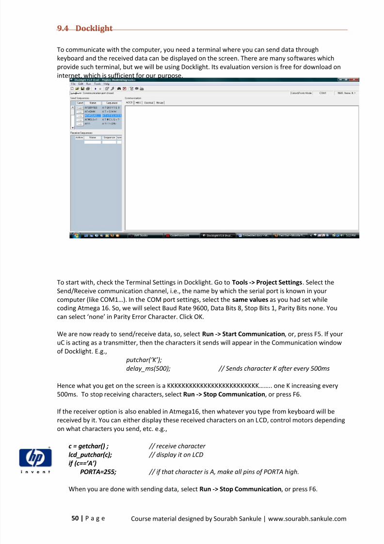
9.4 Docklight
To communicate with the computer, you need a terminal where you can send data throughkeyboard and the received data can be displayed on the screen. There are many softwares whichprovide such terminal, but we will be using Docklight. Its evaluation version is free for download oninternet, which is sufficient for our purpose.
To start with, check the Terminal Settings in Docklight. Go to Tools -> Project Settings . Select theSend/Receive communication channel, i.e., the name by which the serial port is known in yourcomputer (like COM1…). In the COM port settings, select the same values as you had set whilecoding Atmega 16. So, we will select Baud Rate 9600, Data Bits 8, Stop Bits 1, Parity Bits none. Youcan s elect ‘none’ in Parity Error Character. Click OK.
We are now ready to send/receive data, so, select Run -> Start Communication , or, press F5. If youruC is acting as a transmitter, then the characters it sends will appear in the Communication windowof Docklight. E.g.,
putchar(‘ K ’); delay_ms(500); // Sends character K after every 500ms
Hence what you get on the screen is a KKKKKKKKKKKKKKKKKKKKKKKKK…….. one K increasing every500ms. To stop receiving characters, select Run -> Stop Communication , or press F6.
If the receiver option is also enabled in Atmega16, then whatever you type from keyboard will bereceived by it. You can either display these received characters on an LCD, control motors dependingon what characters you send, etc. e.g.,
c = getchar() ; // receive character lcd_putchar(c); // display it on LCDif (c==’A’)
PORTA=255; // if that character is A, make all pins of PORTA high.
When you are done with sending data, select Run -> Stop Communication , or press F6.

8/6/2019 Course Manual - 2010
http://slidepdf.com/reader/full/course-manual-2010 51/71
51 | P a g e Course material designed by Sourabh Sankule | www.sourabh.sankule.com
Chapter 10 Timers
10.1 Basic Theory
Atmega 16 has following timers,
Timer 0, 8 bit Timer 1, 16 bit consisting of two 8 bit parts, A and B Timer 2, 8 bit
Now there are two clocks,
1. System Clock (fs): This is the clock frequency at which Atmega is running. By default it is 1 MHzwhich can be changed by setting fuse bits.
2. Timer Clock (ft): This is the clock frequency at which timermodule is running. Each timer module has different clocks.
Now ft can be in ratios of fs. That is, ft = fs, fs/8, fs/64 ...
For example, if we keep fs = 8 MHz then available options for ftare: 8 MHz, 1 MHz, 125 KHz ... (look in the image)
There are total 4 settings for Timers,
1. Clock Source: Source for timer clock, keep it as systemclock. You can also provide external clock. Read datasheetfor more information about external clock source.
2. Clock value: This is value of ft. Drop down for availableoptions of ft. Chose whichever is required
3. Mode: There are many modes of timers. We will bediscussing following 2 modes,
a. Fast PWM top = FFhb. CTC top=OCRx (x=0, 1A, 2)
4. Output : Depending upon the mode we have chosen there
are options for output pulse. We will look in detail later.
Basically each Timer has a counter unit with size 8 bit for Timer 0, 2 and 16 bit for Timer 1. I will betalking about Timer 0 and same will follow for other Timers.
Each counter has a register which increments by one on every rising edge of timer clock. Aftercounting to its full capacity, 255 for 8 bit, it again starts from 0. By using this register we can havedifferent modes.
Timer/Counter ( TCNT0) and Output Compare Register ( OCR0) are 8-bit registers.
TOP: The counter reaches the TOP when it becomes equal to the highest value in the countsequence. The TOP value can be assigned to be the fixed value 0xFF (MAX) or the value stored inthe OCR0 Register. The assignment is dependent on the mode of operation.

8/6/2019 Course Manual - 2010
http://slidepdf.com/reader/full/course-manual-2010 52/71
52 | P a g e Course material designed by Sourabh Sankule | www.sourabh.sankule.com
F = Ft / 256
D = OCR0 / 255 (non inverted)
D = (255-OCR0) / 255 (inverted)
10.2 Fast PWM Mode
PWM = Pulse Width Modulation.
This mode is used to generate pulse with
Fixed Frequency (F)
Variable Duty Cycle (D)
By changing OCR0 value we can change the duty cycle of theoutput pulse.
As OCR0 is an 8bit register it can vary from 0 o 255.
0 ≤ OCR0 ≤ 255
Pins for Output pulse,
Timer 0 : OC0, pin 4Timer 1A : OC1A, pin 19Timer 1B : OC1B, pin 18Timer 2 : OC2, pin 21
Figure 20: Fast PWM mode Timing Diagram

8/6/2019 Course Manual - 2010
http://slidepdf.com/reader/full/course-manual-2010 53/71
53 | P a g e Course material designed by Sourabh Sankule | www.sourabh.sankule.com
F =
D = 0.5
10.3 CTC Mode
CTC = Clear Timer on Compare Match.
This mode is to generate pulse with,
Fixed Duty Cycle (D = 0.5)
Variable Frequency (F)
By changing value of OCR0 we can change the value of output pulse frequency. As OCR0 is an 8bit register it canvary from 0 to 255.
0 ≤ OCR0 ≤ 255
Figure 21: CTC Mode timing diagram

8/6/2019 Course Manual - 2010
http://slidepdf.com/reader/full/course-manual-2010 54/71
54 | P a g e Course material designed by Sourabh Sankule | www.sourabh.sankule.com
MOSIMISO
SCK
Chapter 11 SPI: Serial Peripheral Interface
11.1 Theory of Operation
The Serial Peripheral Interface Bus or SPI bus is a synchronous serial data link used to communicatebetween two or more microcontroller and devices supporting SPI mode data transfer. Devicescommunicate in master/slave mode where the master device initiates the data frame. Multiple slavedevices are allowed with individual slave select (chip select) lines.
This communication protocol consists of folliwng lines or pins,
1. MOSI : Master Out Slave In (Tx for Master and Rx for Slave)2. MISO : Master In Slave Out (Rx for Master Tx for Slave)3. SCK : Serial Clock (Clock line)4. SS : Slave Select (To select Slave chip) (if given 0 device acts as slave)
Master: This device provides the serial clock to the other device for data transfer. As a clock is usedfor the data transfer, this protocol is Synchronous in nature. SS for Master will be disconnected.
Slave: This device accepts the clock from master device. SS for this has to be made 0 externally.
Pin connections for SPI protocol
MOSIMISOSCKSS0
Master Slave
Figure 22: SPI Data Communication
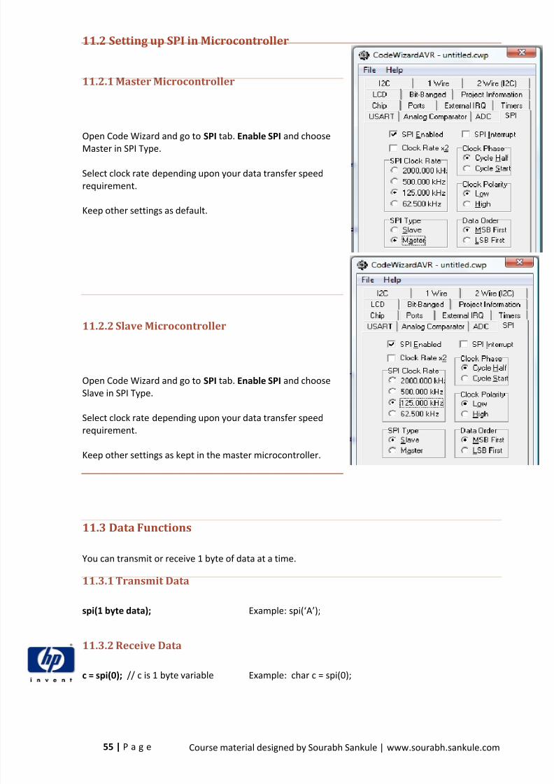
8/6/2019 Course Manual - 2010
http://slidepdf.com/reader/full/course-manual-2010 55/71
55 | P a g e Course material designed by Sourabh Sankule | www.sourabh.sankule.com
11.2 Setting up SPI in Microcontroller
11.2.1 Master Microcontroller
Open Code Wizard and go to SPI tab. Enable SPI and chooseMaster in SPI Type.
Select clock rate depending upon your data transfer speedrequirement.
Keep other settings as default.
11.2.2 Slave Microcontroller
Open Code Wizard and go to SPI tab. Enable SPI and chooseSlave in SPI Type.
Select clock rate depending upon your data transfer speedrequirement.
Keep other settings as kept in the master microcontroller.
11.3 Data Functions
You can transmit or receive 1 byte of data at a time.
11.3.1 Transmit Data
spi(1 byte data); Example : spi(‘A’);
11.3.2 Receive Data
c = spi(0); // c is 1 byte variable Example: char c = spi(0);

8/6/2019 Course Manual - 2010
http://slidepdf.com/reader/full/course-manual-2010 56/71
56 | P a g e Course material designed by Sourabh Sankule | www.sourabh.sankule.com
Chapter 12 ADC: Analog to Digital Converter
12.1 Theory of operation
What we have seen till now that the input given to uC was digital, i.e., either +5 V (logic 1) or 0V(logic 0). But what if we have an analog input, i.e., value varies over a range, say 0V to +5V? Then werequire a tool that converts this analog voltage to discrete values. Analog to Digital Converter (ADC)is such a tool.
ADC is available at PORTA of Atmega16. Thus we have 8 pins available where we can applyanalog voltage and get corresponding digital values. The ADC register is a 10 bit register, i.e., thedigital value ranges from 0 to 1023. But we can also use only 8 bit out of it (0 to 255) as too muchprecision is not required.
Reference voltage is the voltage to which the ADC assigns the maximum value (255 in case of 8bit and 1023 for 10 bit). Hence, the ADC of Atmega16 divides the input analog voltage range (0V toReference Voltage) into 1024 or 256 equal parts, depending upon whether 10 bit or 8 bit ADC isused. For example, if the reference voltage is 5V and we use 10bit ADC, 0V has digital equivalent 0,+5V is digitally 1023 and 2.5V is approximately equal to 512.
12.2 Setting up Microcontroller
To enable ADC in Atmega16, click on the ADC tab in Code Wizard and enable the checkbox. Youcan also check “use 8 bits” as that is sufficient for our purpose and 10 bit accuracy is not required. If the input voltage ranges from 0 to less than +5V, then apply that voltage at AREF (pin 32) and selectthe Volt. Ref. as AREF pin. But if it ranges from 0 to +5 V, you can select the Volt. Ref. as AVCC pinitself. Keep the clock at its default value of 125 kHz and select the Auto Trigger Source as Free
Running. You can also enable an interrupt function if you require.
ADC =Vin x 255/V ref (8 bit)
ADC =Vin x 1023/V ref (10 bit)

8/6/2019 Course Manual - 2010
http://slidepdf.com/reader/full/course-manual-2010 57/71
57 | P a g e Course material designed by Sourabh Sankule | www.sourabh.sankule.com
12.3 Function for getting ADC
Now when you generate and save the code, all the register values are set automatically alongwith a function:
unsigned char read_adc(unsigned char adc_input).
This function returns the digital value of analog input at that pin of PORTA whose number ispassed as parameter, e.g., if you want to know the digital value of voltage applied at PA3, and then
just call the function as,
read_adc(3);
If the ADC is 8 bit, it will return a value from 0 to 255. Most probably you will need to print it onLCD. So, the code would be somewhat like
int a; char c[10]; // declare in the section of global variables
a=read_adc(3);itoa(a,c);lcd_puts(c);
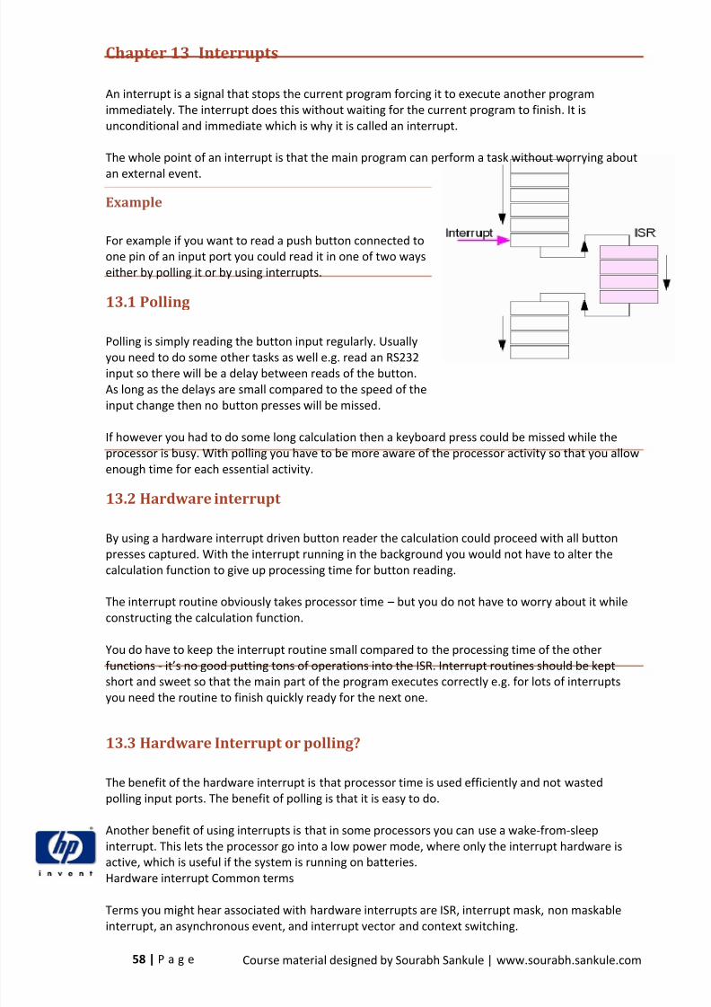
8/6/2019 Course Manual - 2010
http://slidepdf.com/reader/full/course-manual-2010 58/71
58 | P a g e Course material designed by Sourabh Sankule | www.sourabh.sankule.com
Chapter 13 Interrupts
An interrupt is a signal that stops the current program forcing it to execute another programimmediately. The interrupt does this without waiting for the current program to finish. It isunconditional and immediate which is why it is called an interrupt.
The whole point of an interrupt is that the main program can perform a task without worrying about
an external event.
Example
For example if you want to read a push button connected toone pin of an input port you could read it in one of two wayseither by polling it or by using interrupts.
13.1 Polling
Polling is simply reading the button input regularly. Usuallyyou need to do some other tasks as well e.g. read an RS232input so there will be a delay between reads of the button.As long as the delays are small compared to the speed of theinput change then no button presses will be missed.
If however you had to do some long calculation then a keyboard press could be missed while theprocessor is busy. With polling you have to be more aware of the processor activity so that you allowenough time for each essential activity.
13.2 Hardware interrupt
By using a hardware interrupt driven button reader the calculation could proceed with all buttonpresses captured. With the interrupt running in the background you would not have to alter thecalculation function to give up processing time for button reading.
The interrupt routine obviously takes processor time – but you do not have to worry about it whileconstructing the calculation function.
You do have to keep the interrupt routine small compared to the processing time of the otherfunctions - it’s no good putting tons of operations into the ISR. Interrupt routines should be keptshort and sweet so that the main part of the program executes correctly e.g. for lots of interruptsyou need the routine to finish quickly ready for the next one.
13.3 Hardware Interrupt or polling?
The benefit of the hardware interrupt is that processor time is used efficiently and not wastedpolling input ports. The benefit of polling is that it is easy to do.
Another benefit of using interrupts is that in some processors you can use a wake-from-sleepinterrupt. This lets the processor go into a low power mode, where only the interrupt hardware isactive, which is useful if the system is running on batteries.
Hardware interrupt Common terms
Terms you might hear associated with hardware interrupts are ISR, interrupt mask, non maskableinterrupt, an asynchronous event, and interrupt vector and context switching.

8/6/2019 Course Manual - 2010
http://slidepdf.com/reader/full/course-manual-2010 59/71
59 | P a g e Course material designed by Sourabh Sankule | www.sourabh.sankule.com
13.4 Setting up Hardware Interrupt in Microcontroller
There are 3 external interrupts in Atmega 16. They are
INT0 : PD2, Pin 16 INT1 : PD3, Pin 17
INT2 : PB2, Pin 3
There are 3 modes of external Interrupts,
1. Low Level: In this mode interrupt occurs whenever itdetects a ‘0’ logic at INT pin. To use this, you should putan external pull up resistance to avoid interrupt everytime.
2. Falling Edge: In this mode interrupt occurs whenever it detects a falling edge that is ‘1’ to ‘0’logic change at INT pin.
3. Rising Edge: In this mode interrupt occurs whenever it detects a falling edge that is ‘0’ to ‘1’ logicchange at INT pin.
13.5 Functions of Interrupt Service Routine
After generating the code, you can see the following function,
// External Interrupt 0 service routine
interrupt [EXT_INT0] void ext_int0_isr(void)
// Place your code here
You can place your code in the function, and the code will be executed whenever interrupt occurs.
8/6/2019 Course Manual - 2010
http://slidepdf.com/reader/full/course-manual-2010 60/71
60 | P a g e Course material designed by Sourabh Sankule | www.sourabh.sankule.com
Section C
Robotics
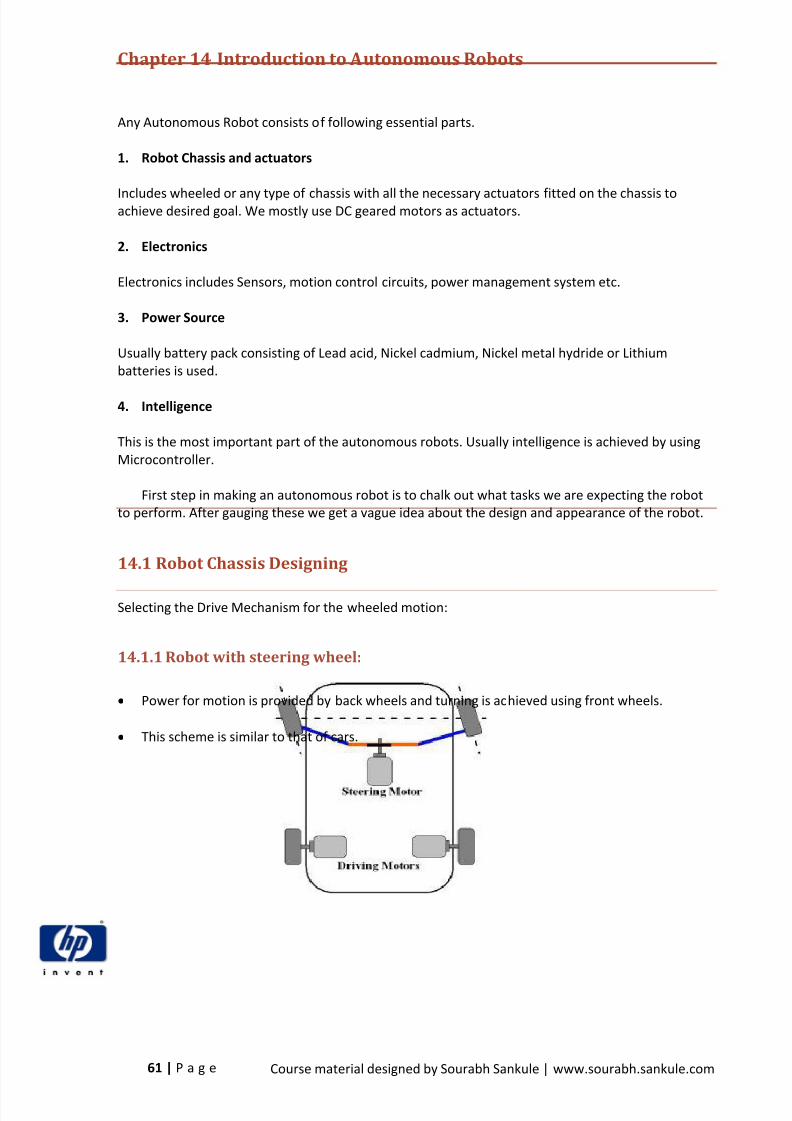
8/6/2019 Course Manual - 2010
http://slidepdf.com/reader/full/course-manual-2010 61/71
61 | P a g e Course material designed by Sourabh Sankule | www.sourabh.sankule.com
Chapter 14 Introduction to Autonomous Robots
Any Autonomous Robot consists of following essential parts.
1. Robot Chassis and actuators
Includes wheeled or any type of chassis with all the necessary actuators fitted on the chassis toachieve desired goal. We mostly use DC geared motors as actuators.
2. Electronics
Electronics includes Sensors, motion control circuits, power management system etc.
3. Power Source
Usually battery pack consisting of Lead acid, Nickel cadmium, Nickel metal hydride or Lithiumbatteries is used.
4. Intelligence
This is the most important part of the autonomous robots. Usually intelligence is achieved by usingMicrocontroller.
First step in making an autonomous robot is to chalk out what tasks we are expecting the robotto perform. After gauging these we get a vague idea about the design and appearance of the robot.
14.1 Robot Chassis Designing
Selecting the Drive Mechanism for the wheeled motion:
14.1.1 Robot with steering wheel:
Power for motion is provided by back wheels and turning is achieved using front wheels.
This scheme is similar to that of cars.

8/6/2019 Course Manual - 2010
http://slidepdf.com/reader/full/course-manual-2010 62/71
62 | P a g e Course material designed by Sourabh Sankule | www.sourabh.sankule.com
Advantages:
1. When path to be followed is straight in nature with curved turns this configuration gives fastestspeed and graceful path following.
2. Don’t need to modify left or right wheels velocity to follow the path. This is very advantageouswhen we want precision velocity control. In this case back wheels take care of velocity controland front wheels take care of direction control.
Disadvantages:
1. It will not able to take very sharp turns. Hence it is difficult to move robot on the grid of lines.
2. Somewhat difficult and expensive to make.
3. Front wheels will need position feedback to control turning control.
14.1.2 Robot with differential drive:
A method of controlling a robot where the left and right wheels are powered independently.
The Three Wheel Differential drive uses two motors and a caster or an omni-directional wheeleasiest to design and program.
The radius and centre of rotation can be varied by the varying the relative speed of rotationbetween the two motors.
Figure 23: Ball bearing caster, wheel based swivel caster and omni directional wheel

8/6/2019 Course Manual - 2010
http://slidepdf.com/reader/full/course-manual-2010 63/71
63 | P a g e Course material designed by Sourabh Sankule | www.sourabh.sankule.com
Rotating the wheels in different directions provides a sharp turn.
For a smooth turn, rotate the wheels in the same direction but with different speeds. Greaterthe difference in speeds, smaller the radius of rotation.
Advantages:
1. Zero turning radius achievable.
2. Easy to move when path to be followed is contoured and zigzag in nature. E.g., navigating alongthe maze of lines.
Disadvantages:
1. If we want to move along curved path we have to control left and right motor’s velocityindependently. Hence precision velocity control becomes difficult as actual velocity of the robotwill be average of the both wheels.
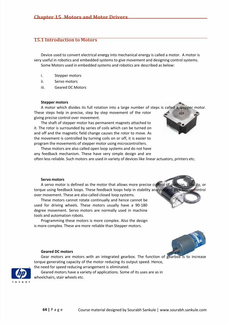
8/6/2019 Course Manual - 2010
http://slidepdf.com/reader/full/course-manual-2010 64/71

8/6/2019 Course Manual - 2010
http://slidepdf.com/reader/full/course-manual-2010 65/71
65 | P a g e Course material designed by Sourabh Sankule | www.sourabh.sankule.com
15.2 H- Bridge:
It is an electronic circuit which enables a voltage to be applied across a load in eitherdirection.
It allows a circuit full control over a standard electric DC motor. That is, with an H-bridge, amicrocontroller, logic chip, or remote control can electronically command the motor to goforward, reverse, brake, and coast.
H-bridges are available as integrated circuits, or can be built from discrete components.
A "double pole double throw" relay can generally achieve the same electrical functionality asan H-bridge, but an H-bridge would be preferable where a smaller physical size is needed,high speed switching, low driving voltage, or where the wearing out of mechanical parts isundesirable.
The term "H-bridge" is derived from the typical graphical representation of such a circuit,which is built with four switches, either solid-state (eg, L293/ L298) or mechanical (eg,relays).
Structure of an H-bridge (highlighted in red)
To power the motor, you turn on two switches that are diagonally opposed.
The two basic states of an H-bridge.
S1 S2 S3 S4 Result1 0 0 1 Motor rotates in one
direction0 1 1 0 Motor rotates in
opposite direction0 0 0 0 Motor free runs
(coasts)0 1 0 1 Motor brakes1 0 1 0 Motor brakes

8/6/2019 Course Manual - 2010
http://slidepdf.com/reader/full/course-manual-2010 66/71
66 | P a g e Course material designed by Sourabh Sankule | www.sourabh.sankule.com
15.3 Motor Driver ICs: L293/L293D and L298
The current provided by the MCU is of the order of 5mA and that required by a motor is~500mA. Hence, motor can’t be controlled directly by MCU and we need an interfacebetween the MCU and the motor.
A Motor Driver IC like L293D or L298 is used for this purpose which has two H-bridge drivers.Hence, each IC can drive two motors.
Note that a motor driver does not amplify the current; it only acts as a switch (An H bridge isnothing but 4 switches).
Drivers are enabled in pairs, with drivers 1 and 2 being enabled by the Enable pin. When anenable input is high (logic 1 or +5V), the associated drivers are enabled and their outputs areactive and in phase with their inputs.
When the enable pin is low, the output is neither high nor low (disconnected), irrespectiveof the input.
Direction of the motor is controlled by asserting one of the inputs to motor to be high (logic1) and the other to be low (logic 0).
To move the motor in opposite direction just interchange the logic applied to the two inputsof the motors.
Figure 25: L293D Figure 24: L298

8/6/2019 Course Manual - 2010
http://slidepdf.com/reader/full/course-manual-2010 67/71

8/6/2019 Course Manual - 2010
http://slidepdf.com/reader/full/course-manual-2010 68/71
68 | P a g e Course material designed by Sourabh Sankule | www.sourabh.sankule.com
Chapter 16 Sensors
16.1 Analog Sensor
The IR analog sensor consists of:
Transmitter : An Infra Red emitting diode
Receiver : A Phototransistor (also referred as photodiode)
It is better to keep R2 as a variac to vary the sensitivity.
The output varies from 0V to 5V depending upon the amount of IR it receives, hence the nameanalog.
The output can be taken to a microcontroller either to its ADC (Analog to Digital Converter) or LM339 can be used as a comparator.

8/6/2019 Course Manual - 2010
http://slidepdf.com/reader/full/course-manual-2010 69/71
69 | P a g e Course material designed by Sourabh Sankule | www.sourabh.sankule.com
16.2 Digital IR Sensor - TSOP Sensor
TSOP 1738 Sensor is a digital IR Sensor; It is logic 1 (+5V) when IR below a threshold is fallingon it and logic 0 (0V) when it receives IR above threshold.
It does not respond to any stray IR, it only responds to IR falling on it at a pulse rate of 38KHz. Hence we have a major advantage of high immunity against ambient light.
No comparator is required and the range of the sensor can be varied by varying the intensityof the IR emitting diode (the variac in figure).

8/6/2019 Course Manual - 2010
http://slidepdf.com/reader/full/course-manual-2010 70/71
70 | P a g e Course material designed by Sourabh Sankule | www.sourabh.sankule.com
Chapter 17 Project Work
17.1 Line following Robot
A Line following robot is a machine which can follow a given path. A Path can be in the form of ablack line on a white surface or reverse of it. The Path can also be in the form of magnetic lineswhich is out of scope of this course. Such robotis a closed loop system having a feedbackmechanism to correct wrong moves. Linefollowing robots can be driven using analogcomparator based circuit like opamp or bymicrocontroller both using feedback fromanalog or digital sensors.
Detection of line is usually done by emittinglight on the surface. If light gets reflected back,then it is white surface else the surface is black.Emission of light is usually done with the help of IR LEDs (Light Emitting Diodes). An array of suchLEDs is used. The emitted light is then receivedusing phototransistors, LDR (Light DependentRegister), TSOP. Based on the value of light received, the received energy is converted to electricalenergy.
If the robot gets off the track, the speed of wheel motors is proportionally varied to make it backon the track.
Line following property of a robot is very useful in designing automated cars. Also, industrialrobots may use such mechanism in order to be on proper path.
Block Diagram for Line Following Robot

8/6/2019 Course Manual - 2010
http://slidepdf.com/reader/full/course-manual-2010 71/71
Chapter 18 References
[1] Atmega 16 Datasheet
[2] www.wikipedia.org
[3] http://www.cmosexod.com/micro_uart.htm
[4] http://www.best-microcontroller-projects.com/hardware-interrupt.html
[5] http://www.avrtutor.com/tutorial/interrupt/interrupts.php