cornerstone electronics technology and robotics i … week16... · cornerstone electronics...
TRANSCRIPT
1
Cornerstone Electronics Technology and Robotics I Week 16 Diodes and Transistor Switches
Administration: o Prayer o Turn in quiz
Review: o Design and wire a voltage divider that divides your +9 V voltage source
into thirds and where the current through all three resistors is approximately 3 mA.
Electricity and Electronics, Section 17.2, Semiconductor Diodes: o A diode is a device designed to permit electron flow in one direction and to
block flow in the other direction. o Structure: A semiconductor diode is made of N-type and P-type
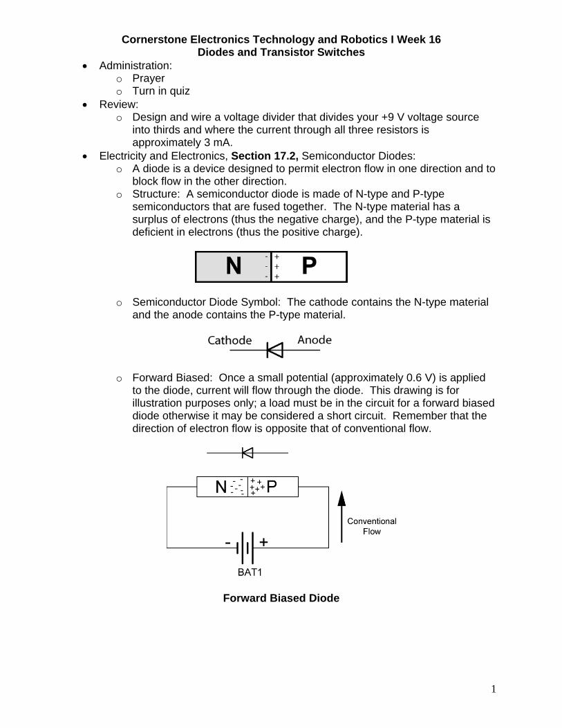
semiconductors that are fused together. The N-type material has a surplus of electrons (thus the negative charge), and the P-type material is deficient in electrons (thus the positive charge).
o Semiconductor Diode Symbol: The cathode contains the N-type material and the anode contains the P-type material.
o Forward Biased: Once a small potential (approximately 0.6 V) is applied to the diode, current will flow through the diode. This drawing is for illustration purposes only; a load must be in the circuit for a forward biased diode otherwise it may be considered a short circuit. Remember that the direction of electron flow is opposite that of conventional flow.
Forward Biased Diode
2
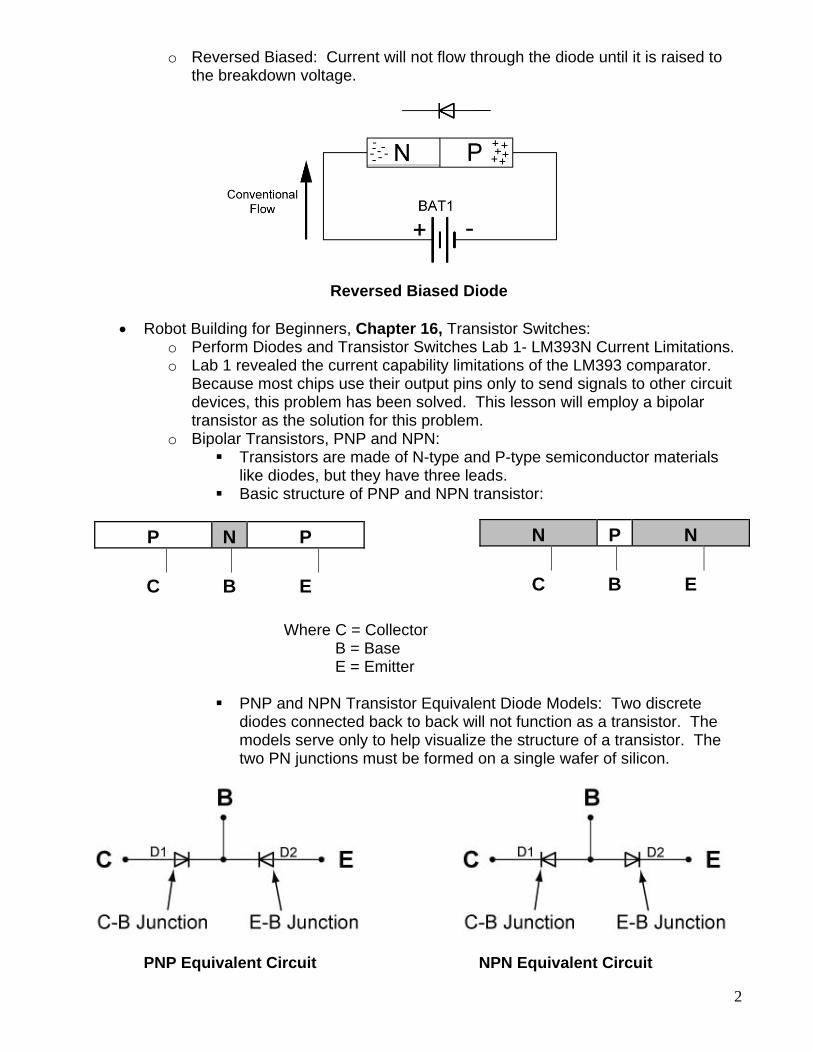
o Reversed Biased: Current will not flow through the diode until it is raised to the breakdown voltage.
Reversed Biased Diode
Robot Building for Beginners, Chapter 16, Transistor Switches: o Perform Diodes and Transistor Switches Lab 1- LM393N Current Limitations. o Lab 1 revealed the current capability limitations of the LM393 comparator.
Because most chips use their output pins only to send signals to other circuit devices, this problem has been solved. This lesson will employ a bipolar transistor as the solution for this problem.
o Bipolar Transistors, PNP and NPN: Transistors are made of N-type and P-type semiconductor materials
like diodes, but they have three leads. Basic structure of PNP and NPN transistor:
P N P
C B E
Where C = Collector B = Base E = Emitter
PNP and NPN Transistor Equivalent Diode Models: Two discrete
diodes connected back to back will not function as a transistor. The models serve only to help visualize the structure of a transistor. The two PN junctions must be formed on a single wafer of silicon.
PNP Equivalent Circuit NPN Equivalent Circuit
N P N
C B E
3
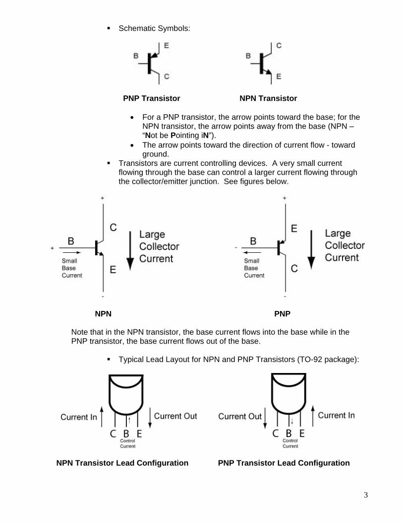
Schematic Symbols:
PNP Transistor NPN Transistor
For a PNP transistor, the arrow points toward the base; for the NPN transistor, the arrow points away from the base (NPN – “Not be Pointing iN”).
The arrow points toward the direction of current flow - toward ground.
Transistors are current controlling devices. A very small current flowing through the base can control a larger current flowing through the collector/emitter junction. See figures below.
NPN PNP
Note that in the NPN transistor, the base current flows into the base while in the PNP transistor, the base current flows out of the base.
Typical Lead Layout for NPN and PNP Transistors (TO-92 package):
NPN Transistor Lead Configuration PNP Transistor Lead Configuration
4
Current in Bipolar Transistors (NPN and PNP):
IE = IC + IB
Where: IE = Emitter current IC = Collector current IB = Base current
Amplification ():
= IC/IB, IC = IB
Where: = Amplification IC = Collector current IB = Base current
See: http://www.learnabout-electronics.org/bipolar_junction_transistors_05.php
Perform Diodes and Transistor Switches Lab 2 – Testing a 2N2222A NPN Transistor.
Sample Sizes: TO-92 SOIC-16 SOT-23 DIP-14
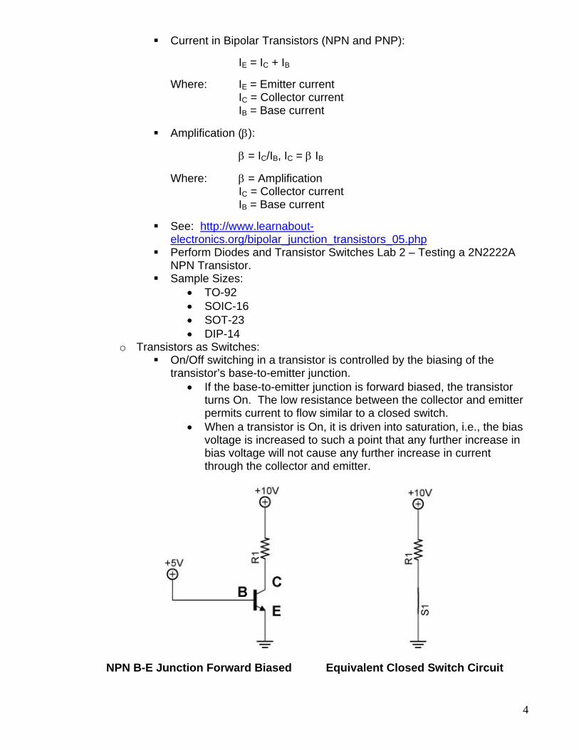
o Transistors as Switches: On/Off switching in a transistor is controlled by the biasing of the
transistor’s base-to-emitter junction. If the base-to-emitter junction is forward biased, the transistor
turns On. The low resistance between the collector and emitter permits current to flow similar to a closed switch.
When a transistor is On, it is driven into saturation, i.e., the bias voltage is increased to such a point that any further increase in bias voltage will not cause any further increase in current through the collector and emitter.
NPN B-E Junction Forward Biased Equivalent Closed Switch Circuit
5
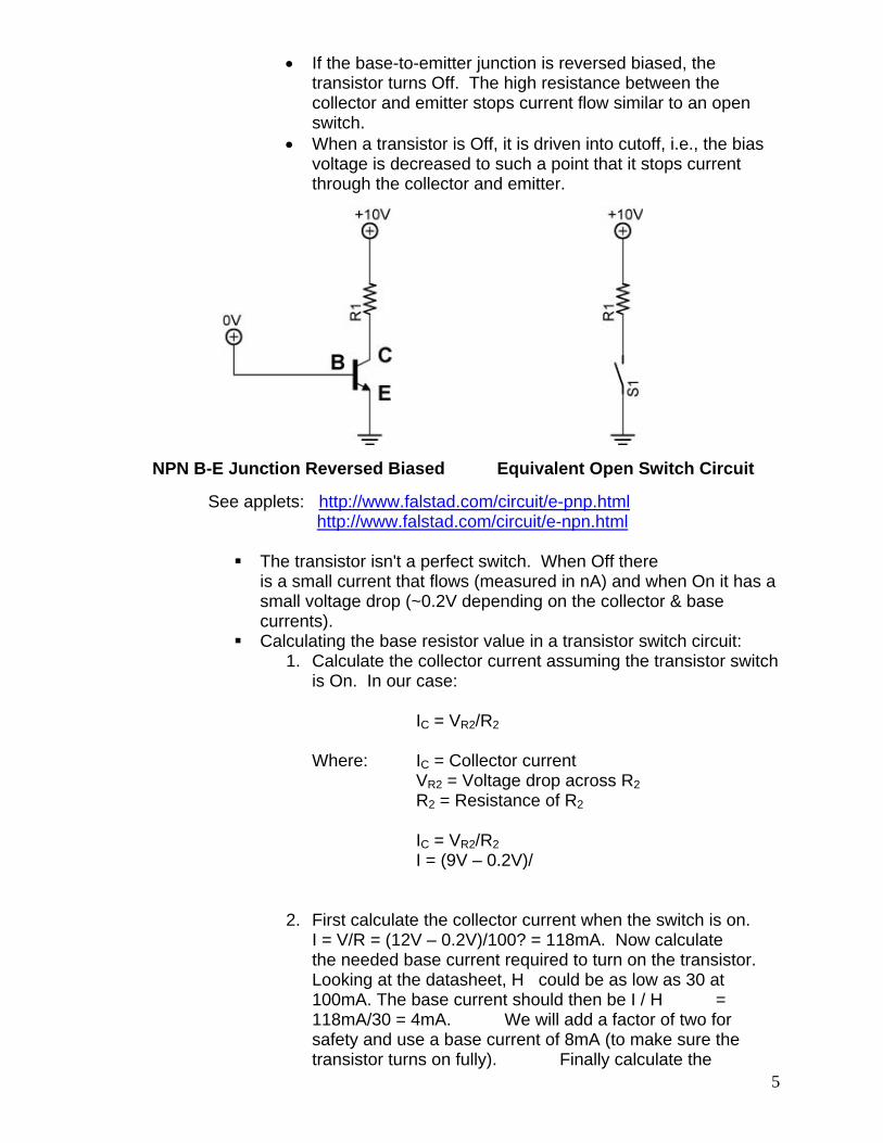
If the base-to-emitter junction is reversed biased, the transistor turns Off. The high resistance between the collector and emitter stops current flow similar to an open switch.
When a transistor is Off, it is driven into cutoff, i.e., the bias voltage is decreased to such a point that it stops current through the collector and emitter.
NPN B-E Junction Reversed Biased Equivalent Open Switch Circuit
See applets: http://www.falstad.com/circuit/e-pnp.html http://www.falstad.com/circuit/e-npn.html
The transistor isn't a perfect switch. When Off there
is a small current that flows (measured in nA) and when On it has a small voltage drop (~0.2V depending on the collector & base currents).
Calculating the base resistor value in a transistor switch circuit: 1. Calculate the collector current assuming the transistor switch
is On. In our case:
IC = VR2/R2
Where: IC = Collector current VR2 = Voltage drop across R2
R2 = Resistance of R2
IC = VR2/R2 I = (9V – 0.2V)/
2. First calculate the collector current when the switch is on. I = V/R = (12V – 0.2V)/100? = 118mA. Now calculate the needed base current required to turn on the transistor. Looking at the datasheet, H could be as low as 30 at 100mA. The base current should then be I / H = 118mA/30 = 4mA. We will add a factor of two for safety and use a base current of 8mA (to make sure the transistor turns on fully). Finally calculate the

6
value for R2, the base resistor. Note: When the transistor is turned on there will be about a 0.7V drop across the base emitter junction. Therefore R2 = V/Ib = (5V – 0.75V)/8mA = 531?. This value isn't critical so use the closest standard value (560?) from http://www.physics.unlv.edu/~bill/PHYS483/transbas.pdf
Perform Diodes and Transistor Switches Lab 3 – NPN and PNP Transistor Load Placement
Perform Diodes and Transistor Switches Lab 4 – NPN and PNP Transistor Switches.
o 2N2907A Transistor: Bipolar PNP general purpose amplifier transistor Data Sheets:
http://www.eletrica.ufsj.edu.br/ensino/eletronica1/pasta/2n2907.pdf
http://www.fairchildsemi.com/ds/PN/PN2907A.pdf The 2N2907A can source 800 mA continuously which is greater
than our needs for the two motors and six LEDs. o See applet: http://www.falstad.com/circuit/e-transswitch.html o Perform Diodes and Transistor Switches Lab 4 – NPN Switch Circuit
Application
7
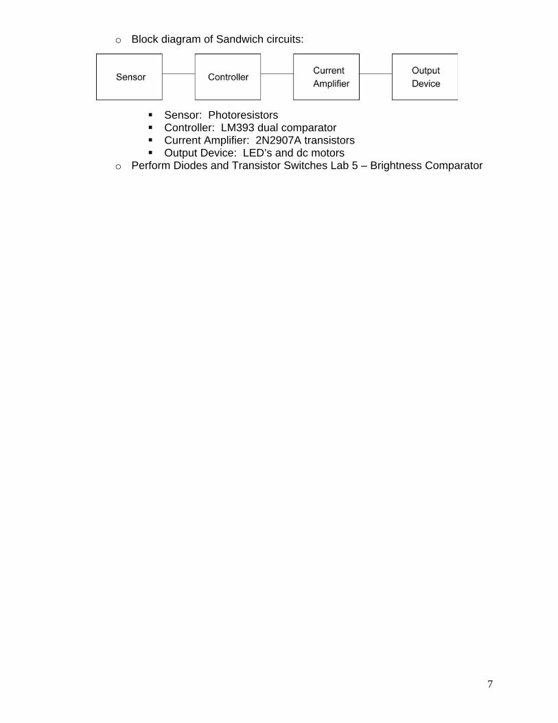
o Block diagram of Sandwich circuits:
Sensor: Photoresistors Controller: LM393 dual comparator Current Amplifier: 2N2907A transistors Output Device: LED’s and dc motors
o Perform Diodes and Transistor Switches Lab 5 – Brightness Comparator
8
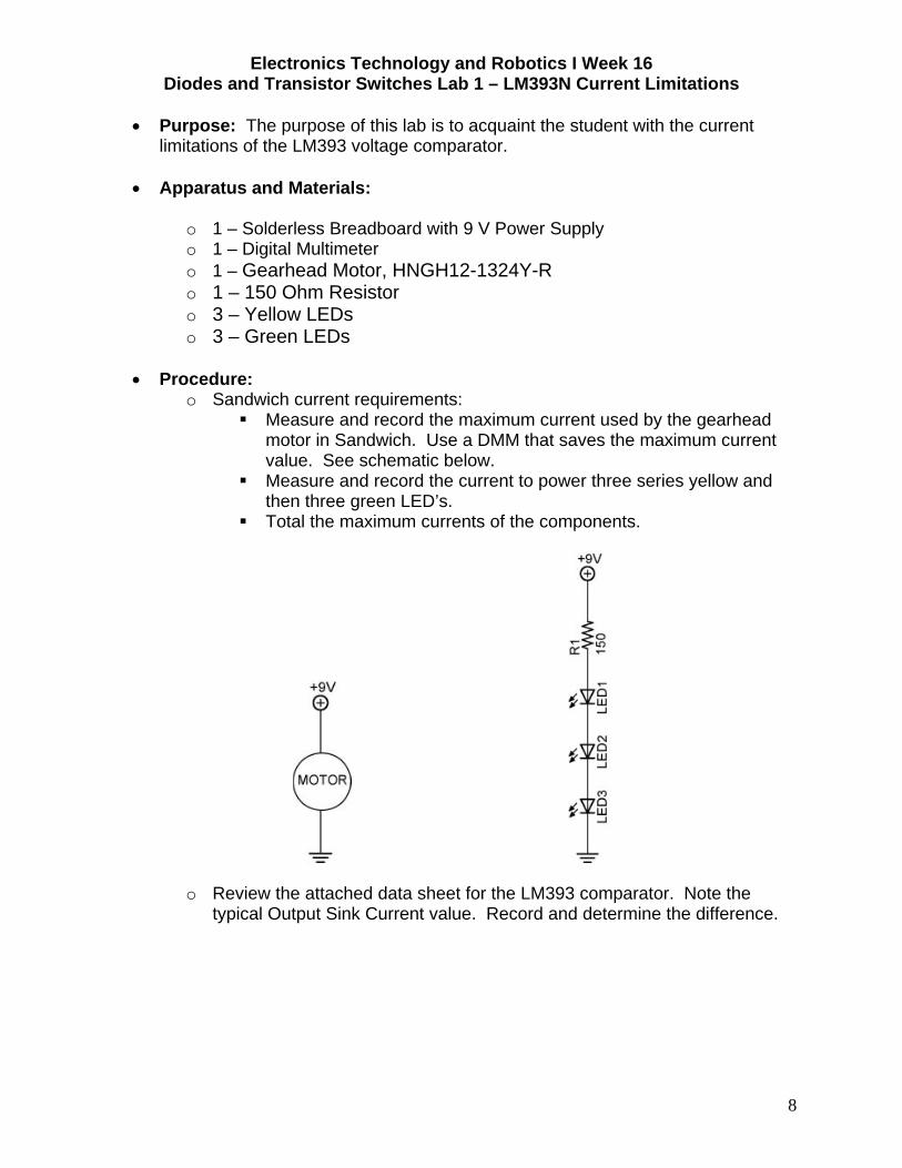
Electronics Technology and Robotics I Week 16 Diodes and Transistor Switches Lab 1 – LM393N Current Limitations
Purpose: The purpose of this lab is to acquaint the student with the current
limitations of the LM393 voltage comparator. Apparatus and Materials:
o 1 – Solderless Breadboard with 9 V Power Supply o 1 – Digital Multimeter o 1 – Gearhead Motor, HNGH12-1324Y-R o 1 – 150 Ohm Resistor o 3 – Yellow LEDs o 3 – Green LEDs
Procedure:
o Sandwich current requirements: Measure and record the maximum current used by the gearhead
motor in Sandwich. Use a DMM that saves the maximum current value. See schematic below.
Measure and record the current to power three series yellow and then three green LED’s.
Total the maximum currents of the components.
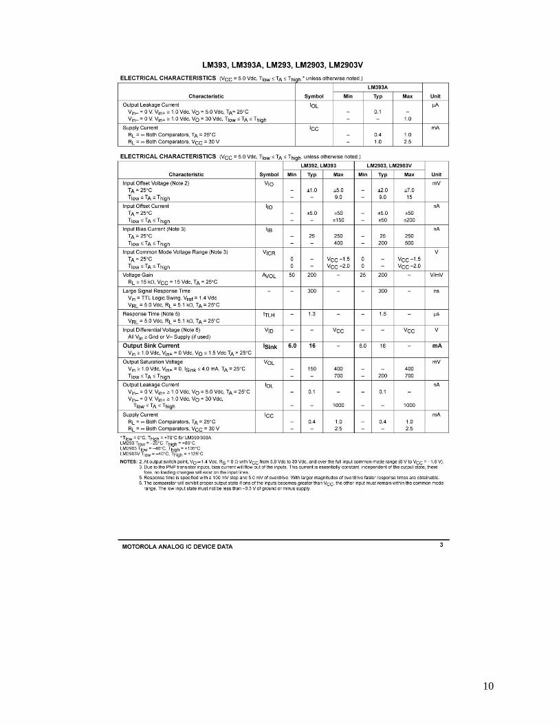
o Review the attached data sheet for the LM393 comparator. Note the typical Output Sink Current value. Record and determine the difference.

9
Results:
Conclusions: o Does the LM393 provide sufficient current output to handle the load
requirements of Sandwich?
10

11
Electronics Technology and Robotics I Week 16 Diodes and Transistor Switches Lab 2 – Testing 2N2222A NPN and 2N2907A PNP Transistors
Purpose: The purpose of this lab is to measure important variables for the operation of a 2N2222A NPN and 2N2907A PNP transistors.
Apparatus and Materials:
o 1 – Solderless Breadboard with 9 V Power Supply o 3 – Digital Multimeters o 1 – 2N2222A NPN Transistor o 1 – 10M, 1M, 820K, 680K, 560K, 470K, 390K, 330K, 270K, 220K,
180K, 150K, 120K, 100K, 47K, 33K, 10K, 3.3K, and 1K Resistors
Procedure: o Build the 2N2222A NPN transistor test circuit below. o Insert the 10M resistor for R1 (the base resistor). o Measure the current into the transistor’s base and collector and also
measure the voltage at the collector with respect to ground. Record your results.
o Substitute all of the other resistors for R1 and repeat the current and voltage measurements. Record your results.
o Calculate and record the for each trial resistor.
o Repeat the above procedure for the 2N2907A PNP transistor.

12
Results: o 2N2222A NPN Transistor:
R1 IB IC VC (mA) (mA) (V)
10M 1M 820K 680K 560K 470K 390K 330K 270K 220K 180K 150K 120K 100K 47K 33K 10K 3.3K 1.0K
13
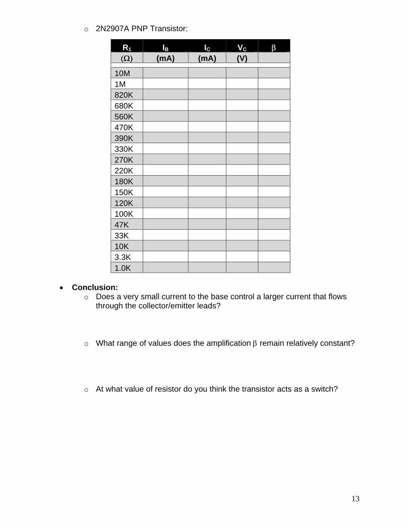
o 2N2907A PNP Transistor:
R1 IB IC VC (mA) (mA) (V)
10M 1M 820K 680K 560K 470K 390K 330K 270K 220K 180K 150K 120K 100K 47K 33K 10K 3.3K 1.0K
Conclusion:
o Does a very small current to the base control a larger current that flows through the collector/emitter leads?
o What range of values does the amplification remain relatively constant?
o At what value of resistor do you think the transistor acts as a switch?
14
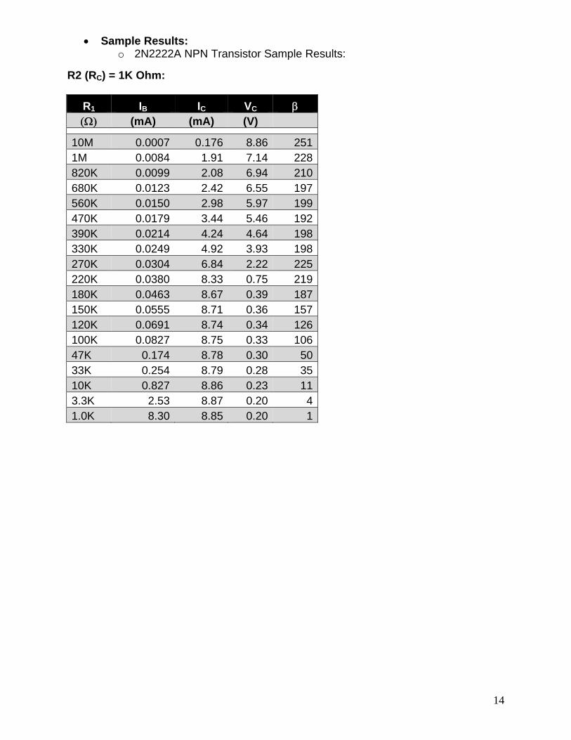
Sample Results: o 2N2222A NPN Transistor Sample Results:
R2 (RC) = 1K Ohm:
R1 IB IC VC (mA) (mA) (V)
10M 0.0007 0.176 8.86 2511M 0.0084 1.91 7.14 228820K 0.0099 2.08 6.94 210680K 0.0123 2.42 6.55 197560K 0.0150 2.98 5.97 199470K 0.0179 3.44 5.46 192390K 0.0214 4.24 4.64 198330K 0.0249 4.92 3.93 198270K 0.0304 6.84 2.22 225220K 0.0380 8.33 0.75 219180K 0.0463 8.67 0.39 187150K 0.0555 8.71 0.36 157120K 0.0691 8.74 0.34 126100K 0.0827 8.75 0.33 10647K 0.174 8.78 0.30 5033K 0.254 8.79 0.28 3510K 0.827 8.86 0.23 113.3K 2.53 8.87 0.20 41.0K 8.30 8.85 0.20 1

15
R2 = 100 Ohm:
R1 IB IC VC (mA) (mA) (V)
#DIV/0!
10M 0.0007 0.177 8.98 2561M 0.0082 1.88 8.80 231820K 0.0099 2.32 8.83 234680K 0.0122 2.86 8.78 234560K 0.0149 3.52 8.71 236470K 0.0179 4.25 8.63 237390K 0.0213 5.09 8.55 239330K 0.0251 6.01 8.45 239270K 0.0305 7.47 8.30 245220K 0.0381 9.34 8.11 245180K 0.0465 11.70 7.88 252150K 0.0555 13.78 7.64 248120K 0.0687 17.05 7.31 248100K 0.0821 20.5 6.92 25047K 0.171 42.4 4.69 24833K 0.245 58.4 3.01 23810K 0.784 79.9 0.90 1023.3K 2.39 79.6 0.83 331.0K 7.93 80.7 0.70 10
Base and Collector Currents through a Random 2N2222A Transistor for a Varity
of Base Resistors (5% Tolerance) (Test setup according to the 2N2222A schematic in this lab.)
16
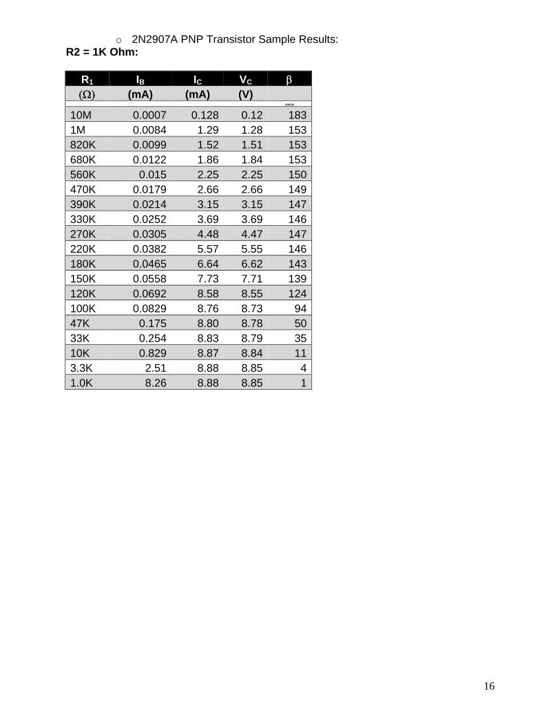
o 2N2907A PNP Transistor Sample Results: R2 = 1K Ohm:
R1 IB IC VC (mA) (mA) (V)
#DIV/0!
10M 0.0007 0.128 0.12 1831M 0.0084 1.29 1.28 153820K 0.0099 1.52 1.51 153680K 0.0122 1.86 1.84 153560K 0.015 2.25 2.25 150470K 0.0179 2.66 2.66 149390K 0.0214 3.15 3.15 147330K 0.0252 3.69 3.69 146270K 0.0305 4.48 4.47 147220K 0.0382 5.57 5.55 146180K 0.0465 6.64 6.62 143150K 0.0558 7.73 7.71 139120K 0.0692 8.58 8.55 124100K 0.0829 8.76 8.73 9447K 0.175 8.80 8.78 5033K 0.254 8.83 8.79 3510K 0.829 8.87 8.84 113.3K 2.51 8.88 8.85 41.0K 8.26 8.88 8.85 1
17
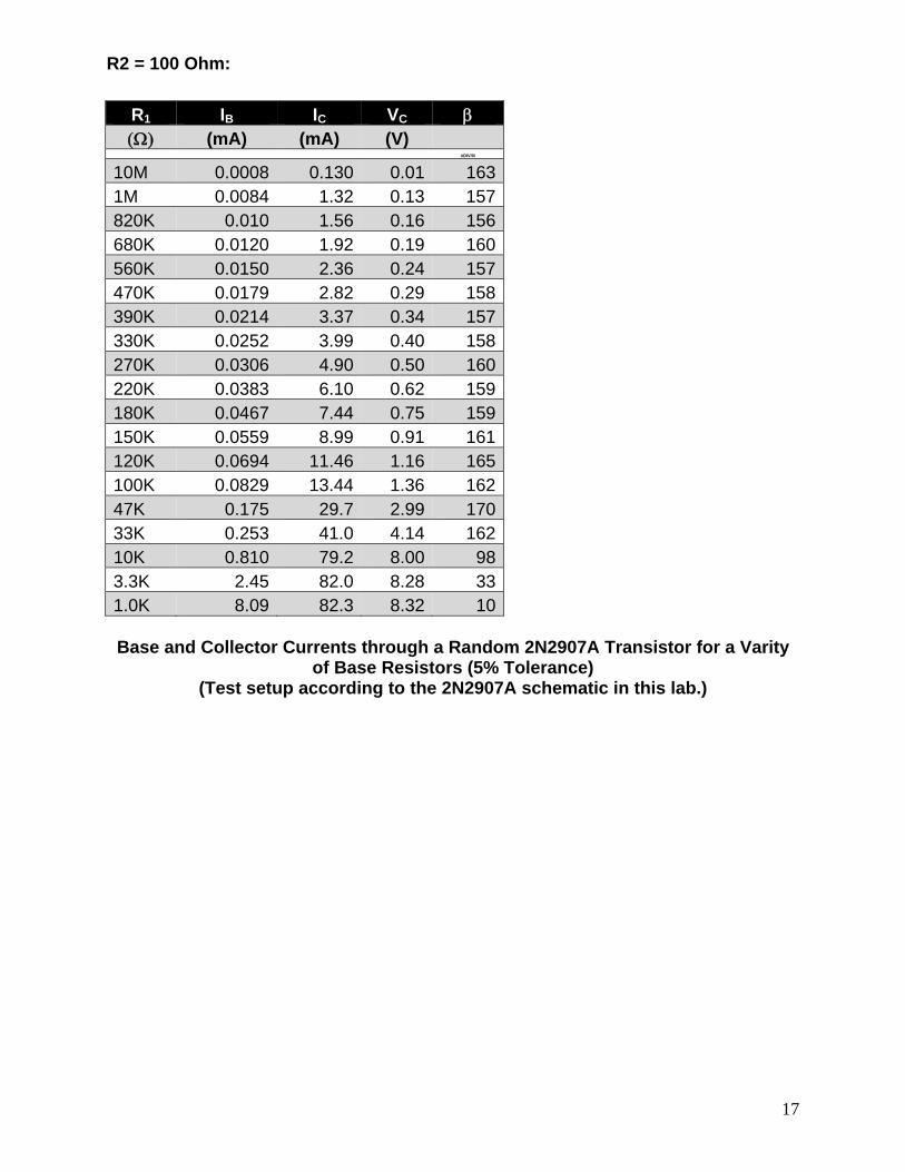
R2 = 100 Ohm:
R1 IB IC VC (mA) (mA) (V)
#DIV/0!
10M 0.0008 0.130 0.01 1631M 0.0084 1.32 0.13 157820K 0.010 1.56 0.16 156680K 0.0120 1.92 0.19 160560K 0.0150 2.36 0.24 157470K 0.0179 2.82 0.29 158390K 0.0214 3.37 0.34 157330K 0.0252 3.99 0.40 158270K 0.0306 4.90 0.50 160220K 0.0383 6.10 0.62 159180K 0.0467 7.44 0.75 159150K 0.0559 8.99 0.91 161120K 0.0694 11.46 1.16 165100K 0.0829 13.44 1.36 16247K 0.175 29.7 2.99 17033K 0.253 41.0 4.14 16210K 0.810 79.2 8.00 983.3K 2.45 82.0 8.28 331.0K 8.09 82.3 8.32 10
Base and Collector Currents through a Random 2N2907A Transistor for a Varity
of Base Resistors (5% Tolerance) (Test setup according to the 2N2907A schematic in this lab.)
18
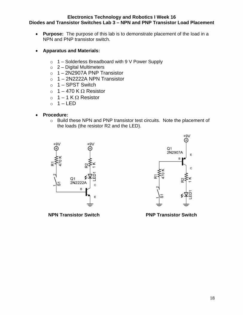
Electronics Technology and Robotics I Week 16 Diodes and Transistor Switches Lab 3 – NPN and PNP Transistor Load Placement
Purpose: The purpose of this lab is to demonstrate placement of the load in a
NPN and PNP transistor switch. Apparatus and Materials:
o 1 – Solderless Breadboard with 9 V Power Supply o 2 – Digital Multimeters o 1 – 2N2907A PNP Transistor o 1 – 2N2222A NPN Transistor o 1 – SPST Switch o 1 – 470 K Resistor o 1 – 1 K Resistor o 1 – LED
Procedure:
o Build these NPN and PNP transistor test circuits. Note the placement of the loads (the resistor R2 and the LED).
NPN Transistor Switch PNP Transistor Switch
19
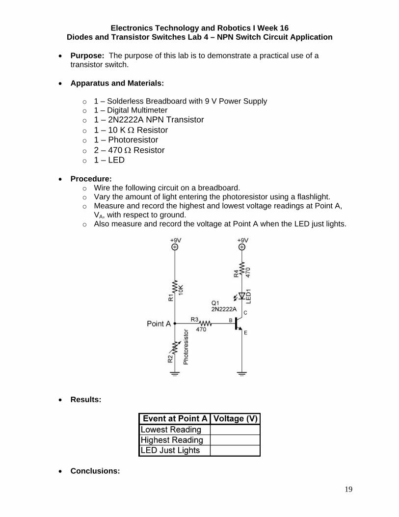
Electronics Technology and Robotics I Week 16 Diodes and Transistor Switches Lab 4 – NPN Switch Circuit Application
Purpose: The purpose of this lab is to demonstrate a practical use of a
transistor switch. Apparatus and Materials:
o 1 – Solderless Breadboard with 9 V Power Supply o 1 – Digital Multimeter o 1 – 2N2222A NPN Transistor o 1 – 10 K Resistor o 1 – Photoresistor o 2 – 470 Resistor o 1 – LED
Procedure:
o Wire the following circuit on a breadboard. o Vary the amount of light entering the photoresistor using a flashlight. o Measure and record the highest and lowest voltage readings at Point A,
VA, with respect to ground. o Also measure and record the voltage at Point A when the LED just lights.
Results:
Conclusions:
20
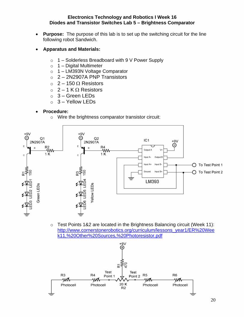
Electronics Technology and Robotics I Week 16 Diodes and Transistor Switches Lab 5 – Brightness Comparator
Purpose: The purpose of this lab is to set up the switching circuit for the line
following robot Sandwich.
Apparatus and Materials:
o 1 – Solderless Breadboard with 9 V Power Supply o 1 – Digital Multimeter o 1 – LM393N Voltage Comparator o 2 – 2N2907A PNP Transistors o 2 – 150 Resistors o 2 – 1 K Resistors o 3 – Green LEDs o 3 – Yellow LEDs
Procedure: o Wire the brightness comparator transistor circuit:
o Test Points 1&2 are located in the Brightness Balancing circuit (Week 11): http://www.cornerstonerobotics.org/curriculum/lessons_year1/ER%20Week11,%20Other%20Sources,%20Photoresistor.pdf