copyrighted material taylor and francis · 158. design of 3d integrated circuits and systems....
TRANSCRIPT

157
6 Emerging Interconnect Technologies for 3D Networks-on-Chip
Rohit Sharma and Kiyoung Choi
6.1 INTRODUCTION
Historically, microchip design has some or all of these functional blocks: computa-tional, storage, communication, and I/O. Microchip technologies have evolved from large-scale integrated (LSI) to very-large-scale integrated (VLSI) to ultra-large-scale integrated (ULSI) systems. The current ULSI technology, where the chip itself constitutes the entire functional system, defines a modern system-on-chip [1]. As per the International Technology Roadmap for Semiconductors (ITRS) projections, with every next-generation technology node, interconnect effects dominate performance. In that, relative delay in global wires could be manyfold longer than that of local wires or logic gates [2]. Process variations, cross talk, and electromagnetic interfer-ence (EMI) can further degrade the performance of these global interconnects. With technology scaling and faster speeds, global synchronization is becoming a mirage. Designers are often required to adopt alternative timing mechanisms including designing globally asynchronous locally synchronous (GALS) chips. While the last decade has seen significantly reduced design cycles, complexity has scaled up several times over the same period of time. Thus, we need a modular approach to design hardware and software, which allows reuse of IPs, so that the key performance met-rics, such as reliability, scalability, energy bounds, and manufacturing costs, are met.
CONTENTS
6.1 Introduction .................................................................................................. 1576.2 3D Integration and 3D Networks-on-Chip ................................................... 160
6.2.1 3D Integrated Circuits ...................................................................... 1606.2.2 3D Networks-on-Chip ...................................................................... 161
6.3 Interconnect Technologies for 3D Networks-on-Chip.................................. 1626.3.1 RF/TSV-Based Interconnect Technology for 3D NoCs ................... 1636.3.2 Optical/Photonics-Based Hybrid 3D NoCs ...................................... 1656.3.3 3D Wireless NoCs ............................................................................ 168
6.4 Summary ...................................................................................................... 171Acknowledgments .................................................................................................. 171References .............................................................................................................. 171
Copyrighted Material - Taylor and Francis
158 Design of 3D Integrated Circuits and Systems
Designing today’s systems-on-chips (SoCs) that perform functions such as digital signal and graphics processing is a complex exercise [3–5]. Most of these SoCs oper-ate on different clock frequencies, thus becoming distributed systems on a single sili-con wafer. This results in a fully distributed communication pattern with no global control. Communication structure in typical SoCs, such as single-chip embedded systems, mobile phones, and HDTVs, could be anything from conventional bus-based to dedicated point-to-point links to ad hoc, irregular networks [1]. However, there are multiple concerns with bus-based communication structures, such as parasitic effects, timing control, limited bandwidth, and arbitration delay [6, 7]. Networks, on the other hand, can be preferred over buses because of higher band-width, pipelining, and multiple concurrent communication support. Also, dedicated point-to-point links may not be a viable solution, as the number of links may increase much faster with increasing number of cores. For many core systems with much less design cycle time, a shared and segmented global communication structure is essential. This in turn would mean that we come up with a segmented SoC com-munication structure with shorter wires for better signal integrity and multiplexed buses for increased throughput and lower energy budget. A network-on-chip (NoC) can be seen as a promising solution for optimum SoC design by integration of many cores that provides answers to some of the above-mentioned design challenges [1, 3].
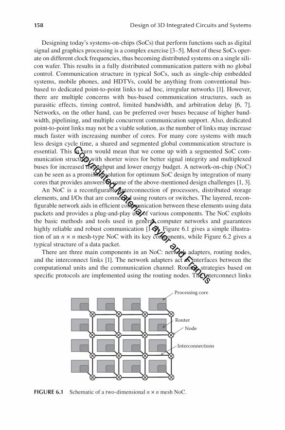
An NoC is a reconfigurable interconnection of processors, distributed storage elements, and I/Os that are connected using routers or switches. The layered, recon-figurable network aids in efficient communication between these elements using data packets and provides a plug-and-play use of various components. The NoC exploits the basic methods and tools used in general computer networks and guarantees highly reliable and robust communication [1–7]. Figure 6.1 gives a simple illustra-tion of an n × n mesh-type NoC with its key components, while Figure 6.2 gives a typical structure of a data packet.
There are three main components in an NoC: network adapters, routing nodes, and the interconnect links [1]. The network adapters act as interfaces between the computational units and the communication channel. Routing strategies based on specific protocols are implemented using the routing nodes. The interconnect links
Processing core
RouterNode
Interconnections
FIGURE 6.1 Schematic of a two-dimensional n × n mesh NoC.
Copyrighted Material - Taylor and Francis

159Emerging Interconnect Technologies for 3D Networks-on-Chip
act as the physical layer and consist of many communication channels. The preferred communication mechanism to transmit data in NoCs is packet switching. NoCs use energy-efficient routing algorithms and tables for optimum packet transmis-sion using routers. Today, NoC designers aspire for the optimum energy-delay-area metric for these routers. The interconnect links (mostly copper wires) are the heart of the physical layer in the NoC. Throughput and energy budget in an NoC are pri-marily determined by these interconnect links. While metal interconnects are by far the most common choice, emerging interconnect technologies like nanophotonics, wireless, optical, and carbon-based interconnects are extensively researched as other alternatives. We shall be discussing the pros and cons of these interconnect technolo-gies in detail in Section 6.3.
The performance and reliability of the network, and thus that of the system, greatly depend on how the network nodes are connected in the physical space, more com-monly known as the topology of the network. The topology determines the foot-print of the NoC, interconnect layout, and size of the router. Broadly, NoC topologies are classified into two types: the regular topologies that offer superior scalability (for example, mesh topology) and the irregular topologies that offer the reverse char-acteristics (for example, star topology) [8]. Dally [9] provided the basic framework of a grid-type k-ary n-cube network topology. Here, k is the degree (number of nodes) of each dimension, while n is the number of the dimensions (for example, 2D, 3D). Thus, what we see in Figure 6.1 represents a 4-ary 2D mesh topology. Another com-monly used regular topology is the torus topology, which differs from mesh topology in terms of the type of interconnect links (ring connections) employed to construct the network. Torus and mesh topologies refer to direct networks, where at least one core is attached to each node. However, there are examples of indirect regular networks, such as the tree topology (binary tree, fat tree, and butterfly tree), that offer hardware efficiency when compared to direct networks [6, 10]. Irregular topologies, on the other hand, have an asymmetric network that scales nonlinearly with respect to energy budget and area requirements [10]. These irregular topologies are more suited for application-specific SoCs that are heterogeneous in nature, with varying sizes, func-tionality, and communication requirements of the computational elements (cores).
Data �itHead �it Tail �it
‐ ……Sourceaddress
Destinationaddress
Physical units or phits
FIGURE 6.2 Typical packet structure.
Copyrighted Material - Taylor and Francis

160 Design of 3D Integrated Circuits and Systems
Summarizing this section, it would be logical to highlight some of the key advantages of NoCs. NoCs can use GALS architecture, thereby avoiding complex global timing requirements. As mentioned earlier, the router efficiently decouples the computational elements (processor cores) with the communication framework. Compared to buses, NoCs use shorter wires that lead to lower energy consumption and lower interconnect parasitics. Further, it is simpler to model shorter wires with reduced design complexities. Reconfigurability in NoCs increases design productivity on the one hand, while reducing design cycle time on the other hand. A reconfigurable network helps the designers to add/remove elements based on requirements, thus pro-viding highly scalable architecture. Wires can be shared using packet switching that results in higher throughput than conventional buses. Over the years, NoC simulation tools have evolved considerably, resulting in lower manufacturing costs. Finally, test-ability is better in NoCs, as they employ efficient error correction schemes.
6.2 3D INTEGRATION AND 3D NETWORKS-ON-CHIP
Continuous devices scaling and performance constraints of global interconnects have led to stacking of multiple dies of integrated circuits (ICs). This vertical stacking has given system designers a window of opportunity to incorporate more functionality into a single package. In this section, we focus on the evolution and advantages of 3D integrated technology and its amalgamation with NoCs to design 3D NoC architec-tures. Further, we highlight the major design constraints that plague the performance of 3D NoCs.
6.2.1 3d integrAted CirCuits
3D ICs provide an answer to the limitations set by long interconnects through stack-ing active silicon layers. These vertically stacked layers lead to reduction in size and number of the global interconnects, offering an opportunity to meet Moore’s law. Therefore, one can expect a significant increase in performance and decrease in power consumption and area with possible integration of CMOS circuits with other technologies [11–13]. 3D ICs offer a number of advantages compared to 2D ICs. These include:
• Shorter global interconnects• Superior performance• Lower power consumption• Higher packing density• Smaller area (footprint)• Scope of mixed-technology ICs
However, 3D ICs have significant concerns in the form of thermal considerations. While the overall power dissipation in 3D ICs may be lower due to shorter and lesser global interconnects, the power density is much higher due to the vertically stacked silicon layers. Thus, efficient thermal management is the key to guarantee the per-formance improvements offered by 3D ICs. For greater understanding on this topic,
Copyrighted Material - Taylor and Francis

161Emerging Interconnect Technologies for 3D Networks-on-Chip
readers are referred to the various thermal management techniques, such as physical design optimization, use of thermal vias, and microfluidic cooling of the vertical stack reported in the literature [14–16].
Vertical integration of chips has also resulted in a paradigm shift in the way we investigate the interconnect technologies by using vertical interconnects for interstrata communication. The vertical interconnect technologies include microbumps, wire bonding, wireless interconnects using capacitive/inductive coupling, and through-silicon vias (TSVs), of which TSVs offer very-high-density vertical interconnects and are by far the most promising technology [13].
6.2.2 3d networKs-on-Chip
By implementation of vertical integration in on-chip networks, one can design 3D NoCs that outperform their 2D counterparts. Figure 6.3 gives a simple illustration highlighting the merger of these two approaches.
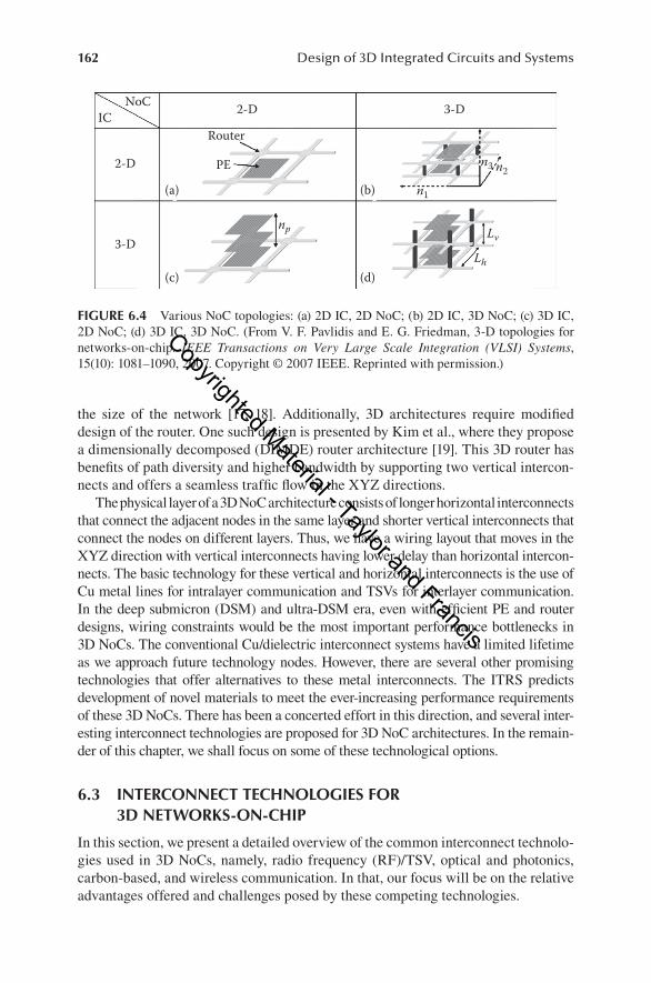
3D NoC architectures are generally classified into two types: symmetric and bus hybrid. However, the latter lacks concurrent communication in the vertical stack and suffers from possible contention and blocking issues in the vertical intercon-nects. The key performance metrics in 3D NoCs include zero-load latency and power consumption of the network. To optimize these two metrics, the authors in [11] have proposed various 3D NoC topologies, which are shown in Figure 6.4.
The 3D IC, 3D NoC topology, as shown in Figure 6.4d, consists of processing elements (PEs) that are integrated over multiple vertical planes and routers, each of which connects two additional neighboring routers (other than the four adjacent in the same plane) located on the adjacent vertical planes. Such a 3D NoC topology significantly minimizes the zero-load latency as well as the power consumption [11]. However, it is important to note that the worst-case performance may not improve by mere transformation of 2D NoC to 3D NoC. This is due to the fact that the worst-case delay is more sensitive to bandwidths offered by the vertical interconnects and
Layer 3
Layer 2
Layer 1
TSVs
FIGURE 6.3 Vertical integration of n × n 2D mesh results in a symmetric 3D mesh NoC.
Copyrighted Material - Taylor and Francis
162 Design of 3D Integrated Circuits and Systems
the size of the network [17, 18]. Additionally, 3D architectures require modified design of the router. One such design is presented by Kim et al., where they propose a dimensionally decomposed (DIMDE) router architecture [19]. This 3D router has benefits of path diversity and higher bandwidth by supporting two vertical intercon-nects and offers a seamless traffic flow in the XYZ directions.
The physical layer of a 3D NoC architecture consists of longer horizontal interconnects that connect the adjacent nodes in the same layer and shorter vertical interconnects that connect the nodes on different layers. Thus, we have a wiring layout that moves in the XYZ direction with vertical interconnects having lower delay than horizontal intercon-nects. The basic technology for these vertical and horizontal interconnects is the use of Cu metal lines for intralayer communication and TSVs for interlayer communication. In the deep submicron (DSM) and ultra-DSM era, even with efficient PE and router designs, wiring constraints would be the most important performance bottlenecks in 3D NoCs. The conventional Cu/dielectric interconnect systems have a limited lifetime as we approach future technology nodes. However, there are several other promising technologies that offer alternatives to these metal interconnects. The ITRS predicts development of novel materials to meet the ever-increasing performance requirements of these 3D NoCs. There has been a concerted effort in this direction, and several inter-esting interconnect technologies are proposed for 3D NoC architectures. In the remain-der of this chapter, we shall focus on some of these technological options.
6.3 INTERCONNECT TECHNOLOGIES FOR 3D NETWORKS-ON-CHIP
In this section, we present a detailed overview of the common interconnect technolo-gies used in 3D NoCs, namely, radio frequency (RF)/TSV, optical and photonics, carbon-based, and wireless communication. In that, our focus will be on the relative advantages offered and challenges posed by these competing technologies.
2-D 3-D
2-D
(a)
(c)
(b)
Router
PE
n1
n3
np Lv
Lh
n2
(d)
3-D
NoCIC
FIGURE 6.4 Various NoC topologies: (a) 2D IC, 2D NoC; (b) 2D IC, 3D NoC; (c) 3D IC, 2D NoC; (d) 3D IC, 3D NoC. (From V. F. Pavlidis and E. G. Friedman, 3-D topologies for networks-on-chip. IEEE Transactions on Very Large Scale Integration (VLSI) Systems, 15(10): 1081–1090, 2007. Copyright © 2007 IEEE. Reprinted with permission.)
Copyrighted Material - Taylor and Francis

163Emerging Interconnect Technologies for 3D Networks-on-Chip
6.3.1 rf/tsv-bAsed interConneCt teChnoLogy for 3d noCs
Among the various interconnect technologies listed above, the use of TSVs is the most promising one and remains the focus of the majority of 3D integration R&D activities. TSVs in 3D NoCs can be used to communicate with the interlayer cores, providing a vertical communication pathway. Compared to other 3D assembly technologies [20], such as wire bonding, metal bumps, and contactless (wireless) coupling, TSVs offer short, low-loss electrical links with a lower footprint and high density. Use of TSVs provides functional benefits, like reduction in the num-ber and length of global wires and integration of disparate technologies. However, the fabrication process of TSVs is a complex and expensive task and mainly gov-erns the integration density and cost [21]. Some of the most widely used TSV fabrication processes include via first (VF), via middle (VM), and via last (VL) processes as shown in Table 6.1.
3D NoC architectures using TSVs can be fabricated using either the monolithic approach or the stacking approach. In the monolithic approach, front-end processing to fabricate the active device layer is repeated on a single wafer. The backend pro-cessing takes care of fabricating the interconnects/TSVs. In the second approach, the individual active device layers are stacked over one another using face-to-face or face-to-back bonding. 3D NoC designs using TSVs show that there is a trade-off between the performance and manufacturing cost. For better thermal management, designers use efficient floor planning where the processors are on one layer below the heat sink, while other components (caches, etc.) are on the other layer, as shown in Figure 6.5. For optimum performance of 3D NoCs, full connectivity between interlayer cores is desired. However, as the number of tiles/nodes increases, there is also an increase in the chip area and manufacturing cost. For example, one would require several hundred TSVs for full layer-layer connectivity of a 4 × 4 mesh-type 3D NoC. If quarter or half layer-layer connectivity is used, the average num-ber of hops increases, thereby severely degrading the network latency and causing communication deadlock [21].
There are several electrical, thermal, and mechanical design issues associated with the use of TSVs in 3D NoCs. From the electrical side, interlayer vertical inter-connections require the design of new router architecture to take into account the additional vertical TSV pathways. The authors in [19] have presented a 3D dimen-sionally decomposed (DimDe) router that supports two additional vertical TSVs and
TABLE 6.1Comparison between Various Via Processes
VF VM VL
Fabrication step TSVs fabricated before CMOS process
TSVs fabricated before BEOL, after CMOS
TSVs fabricated after BEOL process
Diameter <5 µm ~5 µm >5 µm
Density High Medium Low
Cost High Medium Low
Copyrighted Material - Taylor and Francis

164 Design of 3D Integrated Circuits and Systems
optimizes the cost of 3D NoC switches. This modified router uses a partial crossbar switch that supports TSVs and enables concurrent communication between the dif-ferent layers of the 3D NoC. Compared to a full 3D crossbar, there is significant reduction in area, power budget, and logic complexity. The DimDe architecture clearly scores over other architectures and can be used for superior electrical perfor-mance of 3D NoCs. Increased power density per unit area in 3D NoCs results in the heat dissipation of an inner active layer. Routers in 3D NoCs can become a thermal hotspot due to excessive packet transmission and heat generated due to 3D stacking. Thermally aware router architecture design is an important research topic.
It is also important to consider the various thermomechanical issues in 3D NoCs due to the use of TSVs. TSVs are seen to induce a built-in stress that may result in mechanical failures (e.g., delamination, peel, fatigue, etc.) and electrical performance degradation (e.g., parameter shifts, increased variability, EM, etc.). Misalignment during the wafer bonding process and random open defects due to thermal compres-sion should be minimized to guarantee superior TSV yield [22].
While TSVs can provide vertical connection between interlayer cores, high-speed interconnect shortcuts have been proposed for communication between cores on the same layer. These shortcuts can be designed using multiband RF interconnects. The concept of RF interconnects, as explained by the authors in [23], is based on transmission of waves, rather than voltage signaling. When compared to conven-tional transmission line interconnects, RF interconnects achieved significantly lower latency and energy consumption. Thus, one can use RF interconnects overlaid on mesh architecture for intralayer and TSVs for interlayer communication that pro-vides robust and reliable interconnect architecture for 3D NoCs. Although there are several design challenges that need to be addressed, by far, the use of RF/TSV-based interconnect architecture seems to be a promising option for 3D NoCs.
Layer 2 (Processor cores)TSVs
Heat sink for processor cores
Layer 1 (Caches)
P9 P1 P1 P1
P5 P6 P7 P8
P1 P2 P3 P4
C9 C10 C11 C12
C5 C6 C7 C8
C1 C2 !” C4
FIGURE 6.5 Simple illustration of a 3D NoC with separate processor and cache layers. The processor layer is placed below the heat sink.
Copyrighted Material - Taylor and Francis

165Emerging Interconnect Technologies for 3D Networks-on-Chip
6.3.2 optiCAL/photoniCs-bAsed hybrid 3d noCs
In this section, we discuss the use of optical and photonics-based interconnect technology for intra- and interlayer communication in 3D NoCs. The use of optics or optical interconnects for on-chip and chip-chip communication has been a topic of extensive research in the last decade. There has been seminal work that has been reported by authors on the potential benefits of communication using optical media [24, 25]. With continuous scaling in interconnect technology, conventional copper-based interconnects suffer from signal and clock integrity issues. Optical technol-ogy promises to address several physical problems of metal interconnects, including precise clock distribution, system synchronization, bandwidth and density of long interconnections, and reduction of power dissipation. Further, optical interconnects overcome a broad range of design challenges commonly encountered in metallic interconnects, including cross talk, voltage isolation, wave reflection, impedance matching, and pin inductance [25]. While electrical-optical translation costs, CMOS incompatibility, and integration issues were major hindrances at the onset, rapid progress in CMOS-compatible detectors, modulators, and light sources has over-come the initial skepticism about optoelectronic technology [26].
Figure 6.6 gives a simplified schematic of an on-chip optoelectronic interconnec-tion system with associated components, which comprises three major components: a transmitter, a waveguide, and a receiver. The transmitter consists of a laser source, a modulator, and a driver circuit. The laser source provides light to the modulator that converts electrical signals into a modulated optical signal. Waveguides are the optical links (interconnects) through which light gets transmitted. Silicon and poly-mer waveguides are widely used optical links. The optical receiver performs the reverse optical-to-electrical conversion from light to electrical data. It consists of a photodetector, an amplifier stage, and an additional filtering stage for wave division multiplexing.
The situation, however, is different if one intends to connect processor cores in a chip multiprocessor (CMP) using an optical network. Optical bus architecture for com-munication in a CMP was first proposed by the authors in [26] with a loop-shaped bus made of optical waveguides (residing on a dedicated Si layer), as shown in Figure 6.7. There are multiple nodes (or switches) that are connected to the bus, which provide an
Lightsource
Transmitter
Drivercircuit
Waveguide
Opticalinterconnect
Photodetector
Receiver
Ampli�er+
Receiver
FIGURE 6.6 Illustration of an on-chip optical interconnect architecture.
Copyrighted Material - Taylor and Francis

166 Design of 3D Integrated Circuits and Systems
optoelectronic interface between the optical bus and the electrical processor core(s). In this interconnect scheme, the optical loop constitutes the top level of the hierarchy, while the nodes deliver information to processors via electrical sublevels. Such a com-munication scheme requires area- and energy-aware bus topologies. The area budget includes estimates for the active, optical, and metal layers for all possible topologies. In the active layer area, the proposed design accounts for electrical switches in each node, as well as transmitters and receivers on the optical bus. The area occupied in the optical layer is calculated as the sum of the waveguide, modulator, detector, and wave-selective filter areas. The power consumption of the interconnect system is categorized into two components: the power consumed in the electrical sublevels (switches and wiring) and the power consumed in the optical source. It is seen that the area require-ment of the optical layer is the highest, while the power budget is the lowest for all the given topologies. The authors conclude that the four-node configuration is preferable, as the power consumption of the optical components is relatively low compared to that of the electrical subnetwork.
A true 3D optical NoC (ONoC) combines the advantage of optical and 3D tech-nologies providing low latency and high bandwidth with significantly lower power consumption [27–31]. Typically, 3D ONoC is organized in a multilayer configura-tion with an electronic layer consisting of heterogeneous processing elements and routers. One or more layers stacked over this electronic layer provides most of the
Mem Mem
L3 C1 C15 C14
C2
C3
C4
C5
C0
C6 C7 C8 C9L3
L3
L3
MC0
MC1
C13
C11
C12
C10
MC3
MC2
S S
S S
Mem Mem
FIGURE 6.7 Proposed CMP floor plan with an overlaid optical bus. (From N. Kirman et al., Leveraging optical technology in future bus-based chip multiprocessors, In Proceedings of IEEE/ACM International Symposium on Microarchitecture, 2006, pp. 492–503. Copyright © 2006 IEEE. Reprinted with permission.)
Copyrighted Material - Taylor and Francis

167Emerging Interconnect Technologies for 3D Networks-on-Chip
memory storage. The topmost layer is the communication layer that consists of the optical components. Such a hybrid architecture combines the advantages of photonic NoC with 3D integration, where the electronic networks handle smaller packets (data and control), while the optical network handles larger data packets, ensuring lower energy dissipation along with low loss in long optical waveguides. One of the most important components of an ONoC is the design of optical routers with a switching fabric that implements routing and flow control functions at its core. These switch-ing elements can be built using a microresonator. Typically, an n × n optical crossbar requires n2 microresonators and 2n crossing waveguides. Such a crossbar for 3D ONoC has been proposed by the authors in [27, 28] and consists of a data infor-mation processing unit (DIPU) and a control information processing unit (CIPU). Typically, the DIPU is the optical domain, while the CIPU is the traditional CMOS-based electronic domain. As compared to traditional 3D crossbars, we can obtain nearly two-thirds loss reduction by using these 3D optical crossbars. Figure 6.8 gives the schematic of a 3D mesh topology with an overlaid optical network.
For optimum utilization of the optical channel, a connection-oriented commu-nication protocol with a dimension order routing algorithm is preferred. Since opti-cal buffers are not available, the communication protocol ensures that no buffers are required for the optical data. In the above architecture, the routing algorithm and the optimized crossbar design ensure lower delay and better throughput than its 2D counterpart. Network topology plays an important role in the performance of the ONoC. The authors in [30–31] have proposed several wavelength-routed ONoC topologies considering the properties of the optical links as well as their placement constraints. In that, the optical ring-based topology is simpler to design with accept-able power dissipation. However, this topology is limited to target systems with smaller die sizes with simple connectivity requirements.
One major problem with ONoCs is the need for longer waveguides that may result in power loss and back-reflections. Recently, the use of nanophotonic interconnects (NIs) is envisaged for reliable communication between future multicore systems. The on-chip multilayer photonic (OCMP) NoC architecture is an NI-based intercon-nect architecture that consists of 16 decomposed NI-based crossbars placed on four
n × n electronic layer
Overlaid optical fabric
FIGURE 6.8 A 4 × 4 3D architecture with distinct optical and electronic layers. The optical fabric is laid over the electronic layer.
Copyrighted Material - Taylor and Francis

168 Design of 3D Integrated Circuits and Systems
optical communication layers as proposed in [32]. The OCMP architecture removes optical waveguide crossings as well as the use of meandering waveguide placement, thereby reducing optical power losses even further. The NI-based 3D NoC seems to be a promising candidate for future many-core and multicore architectures.
6.3.3 3d wireLess noCs
Wireless communication between interlayer cores in 3D NoCs is quite a radical idea that aims to achieve higher throughput and better latency with lower fabrication and testing costs than those using the conventional TSVs or optical communica-tion. The idea here is to design a hybrid architecture that consists of a conven-tional mesh-based wired topology for communication within individual layers and a vertical wireless channel for interlayer communication. While this concept seems to be a promising alternative, readers must note that it is still in its nascent developmental stage.
In the past, the concept of wireless communication in planar 2D NoCs has been proposed by several researchers. A wireless channel in 2D NoCs works on high-bandwidth, single-hop, long-range communication, as against multihop communi-cation in regular wired NoCs, resulting in lower latency, lower power consumption, and easier routing schemes [29]. The concept of wireless communication in 2D NoCs was first highlighted by Floyd et al. in [33], where a clock distribution net-work was implemented using wireless interconnects. Also, wireless 2D NoCs using an ultrawideband communication scheme have been proposed in [34]. Typically, a wireless channel in a planar NoC has an antenna, network architecture, and trans-ceiver circuits as its basic organizational elements. The idea here is to divide the network into multiple subnets with wired intra-subnet communication and wireless links communicating between the subnets, as shown in Figure 6.9. Each subnet consists of a base station for setting up the wireless link. Unlike traditional wired NoCs, individual subnets in a wireless NoC (WiNoC) can have different architec-tures, thereby having a heterogeneous design that results in significantly improved latency and throughput.
Longer wireless links
Shorter wired links
Basestation
FIGURE 6.9 Hybrid wireless 2D NoC with subnets communicating using wireless links.
Copyrighted Material - Taylor and Francis

169Emerging Interconnect Technologies for 3D Networks-on-Chip
The wireless links are established using mm-wave metallic antennas and infrared carbon nanotube (IR CNT) antennas. Wireless communication for shorter distances (typically 1 mm) may not be more efficient than wired lines. A greater number of wireless nodes will result in area penalty due to several antennas and their associ-ated transceiver circuit. For longer-range wireless communication, metal antennas with zigzag patterns can be used to achieve long-distance (over several millimeters) communication with operating frequencies in tens of GHz [35]. However, careful selection of antenna configuration and dielectric material can increase the operat-ing frequency of the wireless channel in the range of 50–100 GHz. One major issue with mm-wave metal antennas is their area overhead (typically 1–2 mm). In this scenario, nanoscale antennas based on CNTs can provide THz/optical frequency ranges with significantly smaller sizes [36]. The problem, however, is the fact that traditional fabrication techniques are incompatible for overcoming the manufac-turing challenges in CNT-based optical antennas. Even if we expect better control over CNT growth in the coming days, there are several issues associated with this type of communication scheme with respect to establishing interlayer channels for 3D NoCs. The antenna-based communication scheme discussed above propagates surface waves that allow communication between subnets in a 2D architecture. For 3D wireless channels between IPs stacked over each other, we need alternative wireless technologies. One such approach is the use of inductive coupling for verti-cal communication between interlayer IPs.
Inductive coupling has been extensively researched for applications in 3D ICs [37–44]. Davis et al. [37] have used inductive coupling for Fast Fourier Transform (FFT) applications and benchmarked it against other technologies for area and power budget. In [38], the authors have demonstrated a 1 Gbps link between two dies with multiple inductive coupling links. The proposed link outperforms other wireless communication techniques. They further extend the work to obtain 1 Tbps between two layers with minimized cross talk effects [39]. In [40], the authors proposed a bidirectional communication channel for vertical links. The area and power requirements using inductive couplers can be further reduced using burst communication, as shown in [41]. In [42], Choi et al. have proposed chip-to-chip communication using integrator circuits. Wireless communication using inductive coupling has several advantages. The transceiver circuit, including the inductors, can be implemented in a standard CMOS process that is very cost-effective. Tests of individual dies can be performed before they are stacked over each other. Finally, unlike TSV techniques, inductive coupling does not cause any mechanical stresses [37].
The concept of 3D wireless NoC using inductive coupling was first demonstrated by Lee et al. [43]. The proposed architecture assumes a 4 × 4 × 3 3D mesh network, as shown in Figure 6.10a. We have used an integration-based transceiver circuit for inductive coupling. The intralayer links are 32 bits wide, and the routing method is dimensional wormhole routing. Individual routers have eight data transceivers and a single clock transceiver, as shown in Figure 6.10b. The transceiver has separate coils for data and clock transmission with a resultant vertical link of datawidth of 8 bits. The total area of the six-port router in 90 nm technology is 0.13 mm2, which includes an area budget of 0.03 mm2 for the nine coils.
Copyrighted Material - Taylor and Francis

170 Design of 3D Integrated Circuits and Systems
Considering the characteristics of inductive coupling, we proposed a token bus protocol and a global clock transmission scheme. In our proposed approach, only the bottom layer generates a clock and broadcasts it to all layers, including the bot-tom layer itself. Instead of transmitting a data pulse at the rising edge of its local clock, the transmitter sends out the pulse at the rising edge of the broadcast clock. All the receivers generate a sense signal from the same clock received from the bottom layer. Due to the layer-by-layer difference of the timing for the sensing, a delay adjustment circuit is needed. However, since the integration receiver is used, there is a relatively large timing margin, and thus the delay adjustment need not be so precise. For the proposed wireless communication, we decided to use the token bus protocol. As can be figured out from the name, initially one layer has the token and the token holder gets the right to transmit. When a layer is done with transmitting data, or if it has nothing to send, the next layer gets the token. There can be many variations on when to pass the token or how to determine the next token holder. We decided to use a simple method, as follows. Each token
R R
R R
(b)
(a)
North
Data Data Data
Data
Data
West East
Data
Crossbar
Data
Data
South
Up/Down
Clk
R R
R
R RPEtile
R
FIGURE 6.10 System architecture for 3D wireless NoC using inductive coupling: (a) mesh network and (b) router layout for inductive coupling.
Copyrighted Material - Taylor and Francis

171Emerging Interconnect Technologies for 3D Networks-on-Chip
holder sends one full packet, and then broadcasts an announcement such that the upper layer (wraps around from the top to the bottom) gets the token. We can solve the valid signal problem using the header flit containing type, source, destina-tion, and packet size information. If the type indicates that the packet is just for an announcement, other layers will know that the transmitter layer has nothing to send and the token will be passed. Our proposed scheme obtained aggregate throughput of 4.7 flits per cycle under uniform random traffic, which was 78% higher than that for the naive time division scheme. The proposed scheme also outperformed the time division scheme in terms of latency. Overall, this scheme looks promising for wireless communication in 3D NoCs. However, one needs to investigate several issues associated with its implementation and its concurrent use in 2D communication over the same network.
6.4 SUMMARY
This chapter proposes the various interconnect technologies that can be used for communication between vertically stacked IPs in 3D NoCs. Overall, we have seen that three major technologies are potential candidates. In the traditional copper-based wired domain, the most widely used technology is TSVs that form vertically wired channels. However, TSVs suffer from thermal and mechanical issues that need to be addressed. In the optical technology domain, power loss can be a major design issue that can be addressed by employing NI-based interconnect channels. Finally, inductive coupling-based wireless channels for vertical communication can be another alternative technology. The authors feel that an optimum 3D NoC intercon-nect scheme should have a mix of some or all of these disparate technologies. One way to look at this would be a true hybrid architecture where the planar interconnec-tions are the traditional transmission lines, while the vertical interconnects could be one of the above interconnect technologies. For the moment, this is an open research topic that needs further investigations to answer this question.
ACKNOWLEDGMENTS
The authors gratefully acknowledge the technical help and support received from the members of the Design Automation Lab at Seoul National University. The authors also thank Dr. Noriyuki Miura of the Kuroda Lab at Keio University for the deep technical insight provided on wireless communication in 3D ICs using through-chip interface technology.
REFERENCES
1. T. Bjerregaard and S. Mahadevan, A survey of research and practices of network-on-chip, ACM Computing Surveys, 38(1): 1–51, 2006.
2. International Technology Roadmap for Semiconductors, 2011, www.itrs.net. 3. D. Geer, Networks on processors improve on-chip communications, Computer, 42(3):
17–20, 2009. 4. L. Benini and G. De Micheli, Networks on chips: a new SoC paradigm, Computer,
35(1): 70–78, 2002.
Copyrighted Material - Taylor and Francis

172 Design of 3D Integrated Circuits and Systems
5. W. J. Dally and B. Towles, Route packets, not wires: on-chip interconnection networks, In Proceedings of Design Automation Conference, 2001, pp. 684–689.
6. P. Guerrier and A. Greiner, A generic architecture for on-chip packet-switched intercon-nections, In Proceedings of Design, Automation and Test in Europe Conference and Exhibition, 2000, pp. 250–256.
7. J. Cong, An interconnect-centric design flow for nanometer technologies, In Proceedings of the IEEE, 89(4): 505–528, 2001.
8. T. Sharma, Fault tolerant network on chips topologies, University of Stuttgart, 2009. 9. W. J. Dally, Performance analysis of k-ary n-cube interconnection networks, IEEE
Transactions on Computers, 39(6): 775–785, 1990. 10. P. P. Pande, C. Grecu, M. Jones, A. Ivanov, and R. Saleh, Effect of traffic localization
on energy dissipation in NoC-based interconnect, In IEEE International Symposium on Circuits and Systems, 2005, vol. 2, pp. 1774–1777.
11. V. F. Pavlidis and E. G. Friedman, 3-D topologies for networks-on-chip, IEEE Transactions on Very Large Scale Integration (VLSI) Systems, 15(10): 1081–1090, 2007.
12. R. J. Gutmann, J.-Q. Lu, Y. Kwon, J. F. McDonald, and T. S. Cale, Three-dimensional (3D) ICs: a technology platform for integrated systems and opportunities for new poly-meric adhesives, In First International IEEE Conference on Polymers and Adhesives in Microelectronics and Photonics, 2001, pp. 173–180.
13. W. R. Davis, J. Wilson, S. Mick, J. Xu, H. Hao, C. Mineo, A. M. Sule, M. Steer, and P. D. Franzon, Demystifying 3D ICs: the pros and cons of going vertical, IEEE Design and Test of Computers, 22(6): 498–510, 2005.
14. B. Goplen and S. Sapatnekar, Efficient thermal placement of standard cells in 3D ICs using a force directed approach, In International Conference on Computer Aided Design, 2003, pp. 86–89.
15. J. Cong and Y. Zhang, Thermal via planning for 3-D ICs, In IEEE/ACM International Conference on Computer-Aided Design, 2005, pp. 745–752.
16. B. Dang, P. Joseph, M. Bakir, T. Spencer, P. Kohl, and J. Meindl, Wafer-level microflu-idic cooling interconnects for GSI, In Proceedings of the IEEE Interconnect Technology Conference, 2005, pp. 180–182.
17. A.-M. Rahmani, K. R. Vaddina, K. Latif, P. Liljeberg, J. Plosila, and H. Tenhunen, Generic monitoring and management infrastructure for 3D NoC-bus hybrid architec-tures, In IEEE/ACM International Symposium on Networks on Chip (NoCS), 2012, pp. 177–184.
18. Y. Qian, Z. Lu, and W. Dou, From 2D to 3D NoCs: a case study on worst-case com-munication performance, In IEEE/ACM International Conference on Computer-Aided Design—Digest of Technical Papers, 2009, pp. 555–562.
19. J. Kim, et al., A novel dimensionally-decomposed router for on-chip communication in 3D architectures, In Proceedings of International Symposium on Computer Architecture, 2007, pp. 138–149.
20. K. Salah, A. El-Rouby, H. Ragai, and Y. Ismail, 3D/TSV enabling technologies for SOC/NOC: modeling and design challenges, in International Conference on Microelectronics, 2010, pp. 268–271.
21. T. C. Xu, P. Liljeberg, and H. Tenhunen, A study of through silicon via impact to 3D network-on-chip design, In International Conference on Electronics and Information Engineering, 2010, vol. 1, pp. 333–337.
22. I. Loi, S. Mitra, T. H. Lee, S. Fujita, and L. Benini, A low-overhead fault tolerance scheme for TSV-based 3D network on chip links, In IEEE/ACM International Conference on Computer-Aided Design, 2008, pp. 598–602.
23. M. F. Chang, J. Cong, A. Kaplan, M. Naik, G. Reinman, E. Socher, and S.-W. Tam, CMP network-on-chip overlaid with multi-band RF-interconnect, In IEEE 14th International Symposium on High Performance Computer Architecture, 2008, pp. 191–202.
Copyrighted Material - Taylor and Francis

173Emerging Interconnect Technologies for 3D Networks-on-Chip
24. J. W. Goodman, F. J. Leonberger, S.-Y. Kung, and R. A. Athale, Optical interconnections for VLSI systems, Proceedings of the IEEE, 72(7): 850–866, 1984.
25. D. A. B. Miller, Rationale and challenges for optical interconnects to electronic chips, Proceedings of the IEEE, 88(6): 728–749, 2000.
26. N. Kirman, et al., Leveraging optical technology in future bus-based chip multipro-cessors, In Proceedings of IEEE/ACM International Symposium on Microarchitecture, 2006, pp. 492–503.
27. H. Gu and J. Xu, Design of 3D optical network on chip, In Symposium on Photonics and Optoelectronics, 2009, pp. 1–4.
28. Y. Yaoyao, D. Lian, J. Xu, J. Ouyang, M. K. Hung, and Y. Xie, 3D optical networks-on-chip (NoC) for multiprocessor systems-on-chip (MPSoC), In IEEE International Conference on 3D System Integration, 2009, pp. 1–6.
29. L. P. Carloni, P. Pande, and Yuan Xie, Networks-on-chip in emerging interconnect paradigms: advantages and challenges, In 3rd ACM/IEEE International Symposium on Networks-on-Chip, 2009, pp. 93–102.
30. L. Ramini, P. Grani, S. Bartolini, and D. Bertozzi, Contrasting wavelength-routed opti-cal NoC topologies for power-efficient 3D-stacked multicore processors using physical-layer analysis, In Design, Automation and Test in Europe Conference and Exhibition, 2013, pp. 1589–1594.
31. L. Ramini and D. Bertozzi, Power efficiency of wavelength-routed optical NoC topol-ogies for global connectivity of 3D multi-core processors, In Proceedings of Fifth International Workshop on Network on Chip Architectures, 2012, pp. 25–30.
32. R. W. Morris, A. K. Kodi, A. Louri, and R. D. Whaley, Three-dimensional stacked nano-photonic network-on-chip architecture with minimal reconfiguration, IEEE Transactions on Computers, 63(1): 243–255, 2014.
33. B. A. Floyd, C.-M. Hung, and K. K. O, Intra-chip wireless interconnect for clock distri-bution implemented with integrated antennas, receivers and transmitters, IEEE Journal of Solid-State Circuits, 37(5): 543–552, 2002.
34. D. Zhao and Y. Wang, MTNet: design of a wireless test framework for heterogeneous nanometer systems-on-chip, IEEE Transactions on Very Large Scale Integration (VLSI) Systems, 16(8): 1046–1057, 2008.
35. L. Jau, H.-T. Wu, Y. Su, L. Gao, A. Sugavanam, J. E. Brewer, and K. K. O, Communication using antennas fabricated in silicon integrated circuits, IEEE Journal of Solid-State Circuits, 42(8): 1678–1687, 2007.
36. J. Hao and G. W. Hanson, Infrared and optical properties of carbon nanotube dipole antennas, IEEE Transactions on Nanotechnology, 5(6): 766–775, 2006.
37. W. R. Davis, J. Wilson, S. Mick, J. Xu, H. Hao, C. Mineo, A. M. Sule, M. Steer, and P. D. Franzon, Demystifying 3D ICs: the pros and cons of going vertical, IEEE Design and Test of Computers, 22(6): 498–510, 2005.
38. N. Miura, H. Ishikuro, K. Niitsu, T. Sakurai, and T. Kuroda, A 0.14 pJ/b inductive-coupling transceiver with digitally-controlled precise pulse shaping, IEEE Journal of Solid-State Circuits, 43(1): 285–291, 2008.
39. N. Miura, D. Mizoguchi, M. Inoue, K. Niitsu, Y. Nakagawa, M. Tago, M. Fukaishi, T. Sakurai, and T. Kuroda, A 1Tb/s 3W inductive-coupling transceiver for inter-chip clock and data link, In IEEE International Solid-State Circuits Conference, 2006, pp. 1676–1685.
40. Y. Yoshida, N. Miura, and T. Kuroda, A 2Gb/s bi-directional inter-chip data transceiver with differential inductors for high density inductive channel array, In IEEE Asian Solid-State Circuits Conference, 2007, pp. 127–130.
41. N. Miura, Y. Kohama, Y. Sugimori, H. Ishikuro, T. Sakurai, and T. Kuroda, A high-speed inductive-coupling link with burst transmission, IEEE Journal of Solid-State Circuits, 44(3): 947–955, 2009.
Copyrighted Material - Taylor and Francis

174 Design of 3D Integrated Circuits and Systems
42. N. Y. Choi, K.-W. Kwon, and J.-H. Chun, A reliable integrating receiver for inductive coupling chip-to-chip communication, In Proceedings of ITC-CSCC, 2010.
43. J. Lee, M. Zhu, K. Choi, J.-H. Ahn, and R. Sharma, 3D network-on-chip with wireless links through inductive coupling, In 2011 International SoC Design Conference, 2011, pp. 353–356.
44. J. Kim, K. Choi, and G. Loh, Exploiting new interconnect technologies in on-chip com-munication, IEEE Journal on Emerging and Selected Topics in Circuits and Systems, 2(2): 124–136, 2012.
Copyrighted Material - Taylor and Francis