copyright by baolin li 2017
TRANSCRIPT

Copyright
by
Baolin Li
2017
The Thesis Committee for Baolin Li
Certifies that this is the approved version of the following thesis:
Study on House-level Microgrids and Their Power Electronics
APPROVED BY
SUPERVISING COMMITTEE:
Ross Baldick
Surya Santoso
Supervisor:
Study on House-level Microgrids and
Their Power Electronics
by
Baolin Li, B.S.; B.Eng.
Thesis
Presented to the Faculty of the Graduate School of
The University of Texas at Austin
in Partial Fulfillment
of the Requirements
for the Degree of
Master of Science in Engineering
The University of Texas at Austin
May 2017

iv
Acknowledgements
First I would like to thank Professor Baldick for his supervision through my two years of
study, and his revising on my thesis. I would also like to thank Professor Santoso for
spending his time reading my work.
In addition, I would like to thank Dave Tuttle and Hunyoung Shin for their previous work
in this area. I would like to thank Pecan Street Inc for providing the data for research.
Finally, I would like to thank my parents for their constant support.
v
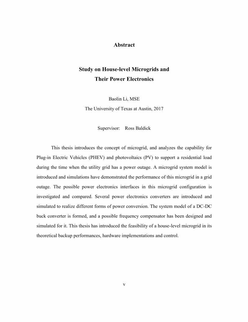
Abstract
Study on House-level Microgrids and
Their Power Electronics
Baolin Li, MSE
The University of Texas at Austin, 2017
Supervisor: Ross Baldick
This thesis introduces the concept of microgrid, and analyzes the capability for
Plug-in Electric Vehicles (PHEV) and photovoltaics (PV) to support a residential load
during the time when the utility grid has a power outage. A microgrid system model is
introduced and simulations have demonstrated the performance of this microgrid in a grid
outage. The possible power electronics interfaces in this microgrid configuration is
investigated and compared. Several power electronics converters are introduced and
simulated to realize different forms of power conversion. The system model of a DC-DC
buck converter is formed, and a possible frequency compensator has been designed and
simulated for it. This thesis has introduced the feasibility of a house-level microgrid in its
theoretical backup performances, hardware implementations and control.

vi
Table of Contents
List of Tables ......................................................................................................... ix
List of Figures ..........................................................................................................x
Chapter 1 Introduction .............................................................................................1
1.1 Background ...............................................................................................1
1.2 Features of Microgrids ..............................................................................2
1.3 Motivations ...............................................................................................3
1.4 Literature Review......................................................................................4
1.4.1 Microgrid Case Study ...................................................................4
1.4.2 Plug-In Vehicle to Home System Study .......................................4
1.4.3 Medium Voltage DC and High Frequency AC System Architectures
.......................................................................................................6
1.4.4 Overview on DC Distribution Systems.........................................6
1.5 Thesis Objectives ......................................................................................7
Chapter 2 V2H System Distributed Generations .....................................................9
2.1 Introduction ...............................................................................................9
2.2 Plug-in Hybrid Electric Vehicles ..............................................................9
2.2.1 From Conventional Vehicles to PHEVs .......................................9
2.2.2 PHEVs in the Market ..................................................................10
2.2.3 PHEV’s Power Interface .............................................................12
2.3 Photovoltaic Panels .................................................................................13
2.3.1 Panel Model ................................................................................13
2.3.2 Panel Power Inverter ...................................................................16
Chapter 3 Simulations of a V2H System ...............................................................17
3.1 Introduction .............................................................................................17
3.2 System Model .........................................................................................17
3.2.1 Load and PV Profile....................................................................17
3.2.2 Scenario Description ...................................................................17
vii
3.2.3 Simulation Scheme .....................................................................18
3.3 Simulation Results ..................................................................................20
3.3.1 Backup Duration .........................................................................20
3.3.2 PV Spillage .................................................................................21
3.3.3 One Particular Backup Event ......................................................21
Chapter 4 Power Electronics Interfaces in V2H System .......................................24
4.1 Introduction .............................................................................................24
4.2 Interfaces in DC and AC Microgrid Configuration ................................24
4.2.1 AC Distribution Microgrid .........................................................24
4.2.2 DC Distribution Microgrid .........................................................25
4.2.3 Comparisons between DC and AC Configurations ....................27
4.3 DC/DC Converter Models ......................................................................28
4.3.1 Buck Converter ...........................................................................28
4.3.1.1 Circuit Topology .............................................................28
4.3.1.2 Buck Converter Simulation.............................................29
4.3.2 Boost Converter ..........................................................................31
4.3.2.1 Circuit Topology .............................................................31
4.3.2.2 Boost Converter Simulation ............................................32
4.3.3 Other DC Converter Topologies .................................................33
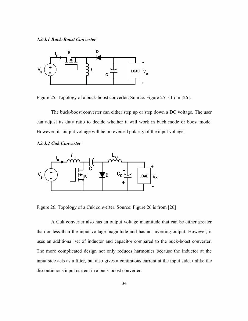
4.3.3.1 Buck-Boost Converter ....................................................34
4.3.3.2 Cuk Converter .................................................................34
4.3.3.3 Bi-directional Converter .................................................35
4.4 DC/AC Converter Models ......................................................................35
4.4.1 Rectifier.......................................................................................35
4.4.1.1 Circuit Model ..................................................................36
4.4.1.2 Rectifier Simulation ........................................................36
4.4.2 Power Inverter .............................................................................39
4.4.2.1 Circuit Model ..................................................................39
4.4.2.2 Inverter Simulation .........................................................40
viii
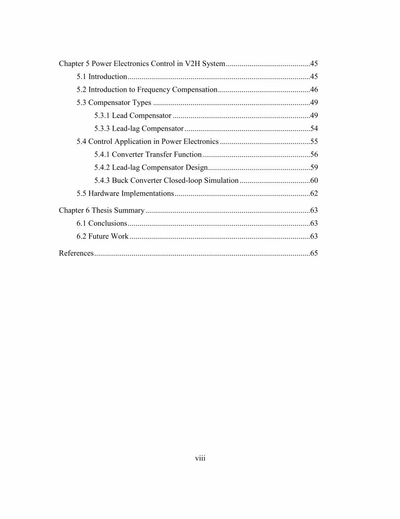
Chapter 5 Power Electronics Control in V2H System ...........................................45
5.1 Introduction .............................................................................................45
5.2 Introduction to Frequency Compensation ...............................................46
5.3 Compensator Types ................................................................................49
5.3.1 Lead Compensator ......................................................................49
5.3.3 Lead-lag Compensator ................................................................54
5.4 Control Application in Power Electronics ..............................................55
5.4.1 Converter Transfer Function .......................................................56
5.4.2 Lead-lag Compensator Design ....................................................59
5.4.3 Buck Converter Closed-loop Simulation ....................................60
5.5 Hardware Implementations .....................................................................62
Chapter 6 Thesis Summary ....................................................................................63
6.1 Conclusions .............................................................................................63
6.2 Future Work ............................................................................................63
References ..............................................................................................................65

ix
List of Tables
Table 1. PHEVs in the market. ..............................................................................11
x
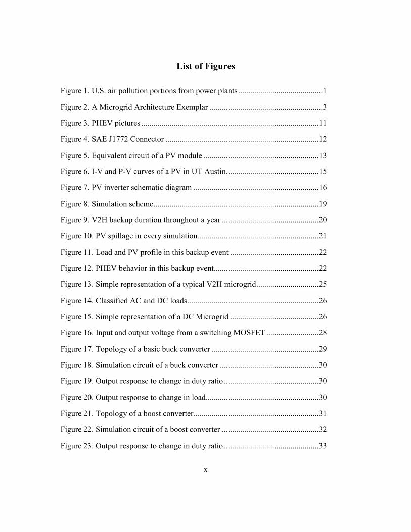
List of Figures
Figure 1. U.S. air pollution portions from power plants ..........................................1
Figure 2. A Microgrid Architecture Exemplar ........................................................3
Figure 3. PHEV pictures ........................................................................................11
Figure 4. SAE J1772 Connector ............................................................................12
Figure 5. Equivalent circuit of a PV module .........................................................13
Figure 6. I-V and P-V curves of a PV in UT Austin..............................................15
Figure 7. PV inverter schematic diagram ..............................................................16
Figure 8. Simulation scheme..................................................................................19
Figure 9. V2H backup duration throughout a year ................................................20
Figure 10. PV spillage in every simulation ............................................................21
Figure 11. Load and PV profile in this backup event ............................................22
Figure 12. PHEV behavior in this backup event....................................................22
Figure 13. Simple representation of a typical V2H microgrid ...............................25
Figure 14. Classified AC and DC loads .................................................................26
Figure 15. Simple representation of a DC Microgrid ............................................26
Figure 16. Input and output voltage from a switching MOSFET ..........................28
Figure 17. Topology of a basic buck converter .....................................................29
Figure 18. Simulation circuit of a buck converter .................................................30
Figure 19. Output response to change in duty ratio ...............................................30
Figure 20. Output response to change in load........................................................30
Figure 21. Topology of a boost converter ..............................................................31
Figure 22. Simulation circuit of a boost converter ................................................32
Figure 23. Output response to change in duty ratio ...............................................33
xi
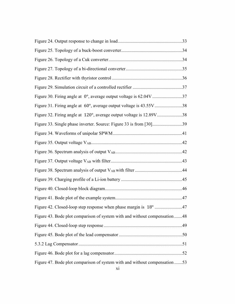
Figure 24. Output response to change in load........................................................33
Figure 25. Topology of a buck-boost converter.....................................................34
Figure 26. Topology of a Cuk converter ................................................................34
Figure 27. Topology of a bi-directional converter .................................................35
Figure 28. Rectifier with thyristor control .............................................................36
Figure 29. Simulation circuit of a controlled rectifier ...........................................37
Figure 30. Firing angle at 0°, average output voltage is 62.04V ..........................37
Figure 31. Firing angle at 60°, average output voltage is 43.55V ........................38
Figure 32. Firing angle at 120°, average output voltage is 12.89V ......................38
Figure 33. Single phase inverter. Source: Figure 33 is from [30]..........................39
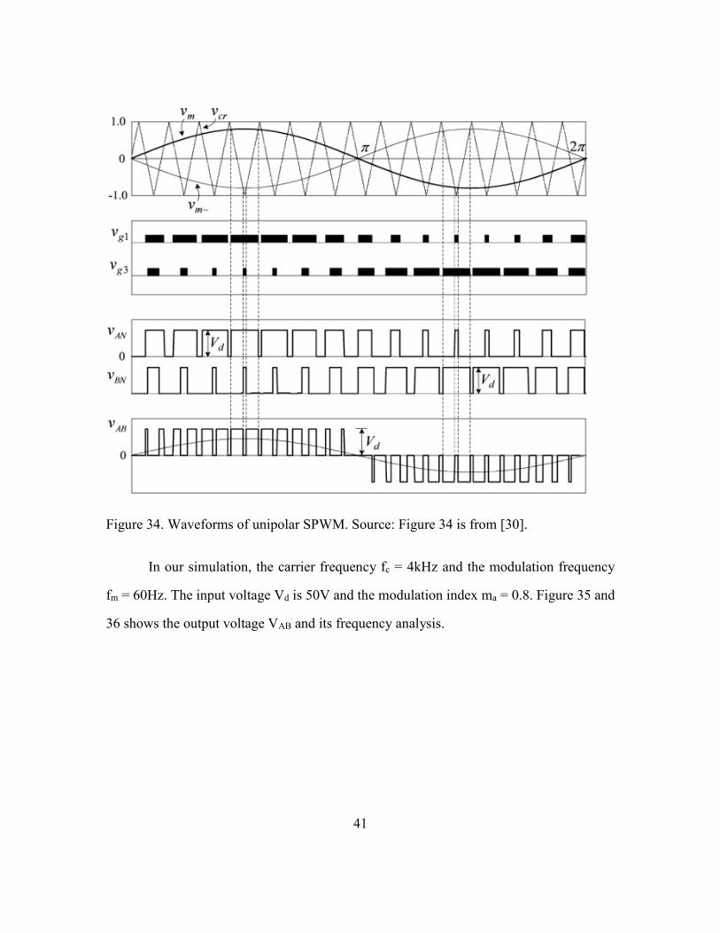
Figure 34. Waveforms of unipolar SPWM ............................................................41
Figure 35. Output voltage VAB ...............................................................................42
Figure 36. Spectrum analysis of output VAB ..........................................................42
Figure 37. Output voltage VAB with filter ..............................................................43
Figure 38. Spectrum analysis of output VAB with filter .........................................44
Figure 39. Charging profile of a Li-ion battery .....................................................45
Figure 40. Closed-loop block diagram...................................................................46
Figure 41. Bode plot of the example system..........................................................47
Figure 42. Closed-loop step response when phase margin is 18° ........................47
Figure 43. Bode plot comparison of system with and without compensation .......48
Figure 44. Closed-loop step response ....................................................................49
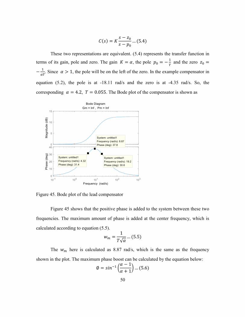
Figure 45. Bode plot of the lead compensator .......................................................50
5.3.2 Lag Compensator ..........................................................................................51
Figure 46. Bode plot for a lag compensator ...........................................................52
Figure 47. Bode plot comparison of system with and without compensation .......53

xii
Figure 48. Closed-loop step response ....................................................................53
Figure 49. Bode plot of a lead-lag compensator ....................................................55
Figure 50. Closed-loop control of a DC/DC converter ..........................................55
Figure 51. Bode plot of example buck converter ...................................................58
Figure 52. Closed-loop step response of example buck converter ........................58
Figure 53. Bode plot of the lead-lag compensator .................................................60
Figure 54. Bode plot of system with and without compensation ...........................61
Figure 55. Closed-loop response of system with and without compensation ........61
Figure 56. Lead compensator circuit .....................................................................62
1
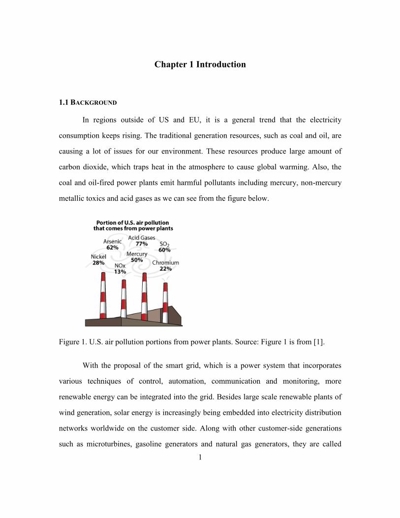
Chapter 1 Introduction
1.1 BACKGROUND
In regions outside of US and EU, it is a general trend that the electricity
consumption keeps rising. The traditional generation resources, such as coal and oil, are
causing a lot of issues for our environment. These resources produce large amount of
carbon dioxide, which traps heat in the atmosphere to cause global warming. Also, the
coal and oil-fired power plants emit harmful pollutants including mercury, non-mercury
metallic toxics and acid gases as we can see from the figure below.
Figure 1. U.S. air pollution portions from power plants. Source: Figure 1 is from [1].
With the proposal of the smart grid, which is a power system that incorporates
various techniques of control, automation, communication and monitoring, more
renewable energy can be integrated into the grid. Besides large scale renewable plants of
wind generation, solar energy is increasingly being embedded into electricity distribution
networks worldwide on the customer side. Along with other customer-side generations
such as microturbines, gasoline generators and natural gas generators, they are called
2
distributed generation (DG) units with capacities typically ranging from 1kW to 100MW.
Customers using DG can have a higher degree of freedom to power their facilities at any
time, or even inject power to the grid [2][3]. With some distributed generation, the
customer can form a small local system called microgrid.
1.2 FEATURES OF MICROGRIDS
The main parts of a microgrid are the interconnected loads and the distributed
generation. The interconnected generation and load is usually attached to a utility grid but
is also able to function independently. Implementations of power electronics and sensors
are required to provide proper monitoring and control.
The feature of a microgrid is that it can operate independently in “off-grid” mode
or as a smaller subset of a utility grid in “grid-tie” mode. In normal conditions, there is an
energy manager that decides the amount of power to draw or inject to the utility grid. A
static transfer switch is an electrical device that when closed allows instantaneous transfer
of power source to load. If there is a fault in the grid, it will switch the microgrid to off-
grid mode to help maintain the power level for customer load [4]. The size of a microgrid
can be flexible: it can be a customer’s own house with his own DG, or a large military
base.
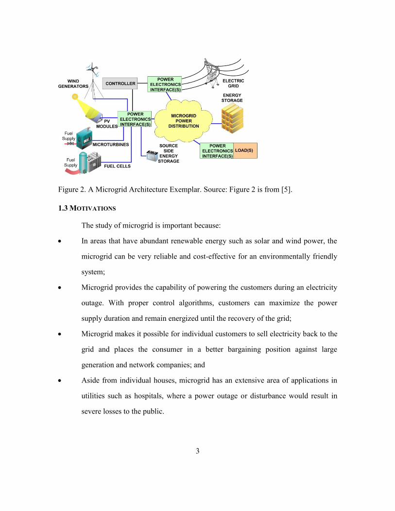
Figure 2 shows an example of microgrid architecture: The whole microgrid is
connected to the utility grid by some power electronics interfaces that can switch
operating modes; the central yellow area works as the “brain” to control the collection
and distribution of power; the distributed energy resources (DER) here include wind
generators, PV modules, microturbines and fuel cells which are connected to the
microgrid power distribution area; the power generated from DER will then be supplied
to local loads, energy storages and, in some cases, the grid.
3
Figure 2. A Microgrid Architecture Exemplar. Source: Figure 2 is from [5].
1.3 MOTIVATIONS
The study of microgrid is important because:
• In areas that have abundant renewable energy such as solar and wind power, the
microgrid can be very reliable and cost-effective for an environmentally friendly
system;
• Microgrid provides the capability of powering the customers during an electricity
outage. With proper control algorithms, customers can maximize the power
supply duration and remain energized until the recovery of the grid;
• Microgrid makes it possible for individual customers to sell electricity back to the
grid and places the consumer in a better bargaining position against large
generation and network companies; and
• Aside from individual houses, microgrid has an extensive area of applications in
utilities such as hospitals, where a power outage or disturbance would result in
severe losses to the public.
4
1.4 LITERATURE REVIEW
1.4.1 Microgrid Case Study
Reference [6] has fully demonstrated a microgrid that was constructed in Sendai,
Japan and how the microgrid helped during an earthquake power outage. The distributed
energy resources were one phosphoric acid fuel cell, two gas turbines and a PV array.
The main energy source in island operation was natural gas. The waste heat from gas
engine were also delivered to residents for heating.
The load was divided into 5 classes (DC, A, B1, B3 and C with priority from high
to low) according to the power quality requirements. When the earthquake occurred, the
utility grid was shut down for 3 days, during which the microgrid was operating in island
mode. The gas engine accidentally stopped working because of control issues, so only
DC load, class A and B1 load were served with the battery and PV. Later on, with battery
storage decreasing, the voltage level cannot satisfy A and B1 load so only DC load was
supplied. After 21 hours of operation, gas engine was fixed and restarted, all classes of
loads were fully supplied. Also, the importance of power diversity and backup equipment
was discussed, since some loads were still supplied given the abnormal operation of gas
engine.
1.4.2 Plug-In Vehicle to Home System Study
The author of [7] has modeled a Vehicle-to-Home(V2H) system composed of a
PHEV generator, battery, PV and load. During off-grid operation, energy production
priorities from high to low are: PV, battery, engine generator until the gasoline is
exhausted. The battery charge/discharge efficiency was obtained and the energy
conversion ratio (ECR) from gasoline to electricity was measured for a Chevrolet Volt
model.
5
This paper also introduced some key power electronics interfaces and control
algorithms needed for a V2H system. In the off-grid mode backup duration simulations,
the control algorithm used was to allow battery State of Charge (SoC) drop to a lower
bound (0%), then the generator charges it to an upper bound (100%) and repeat.
However, a V2H system with PV would have PV spillage when the battery was charged
too full to store the solar energy. Two more optimal strategies were proposed by the
author: one was to lower the SoC upper bound, the other was to cease load supporting
before battery was fully depleted so that the remaining charge can restart PV operation
and then power the load, which has the potential to indefinitely provide power. The
backup duration can be further extended with better demand side response.
Reference [33] has proposed an optimization model in a V2H microgrid to
maximize the backup duration during a grid outage. The author suggested that if we use
the PHEV generator to directly supply the house load, the battery charging and
discharging power loss can be avoided, but the generator has a poor efficiency at a
residential-level power output. Charging the battery at a high-efficiency generator output
range should be more beneficial than serving the load at a low-efficiency range. In the
algorithm proposed, extra PV power is used to charge the battery; If load is greater than
PV generation, the battery is discharged; For the remaining unsatisfied load, the generator
will directly serve the load if it is large enough, or serve the load while charging the
battery if the load is small. The author also extended his model to a Vehicles-to-Homes
(Vs2Hs) model which enables power backup to homes using shared distributed
generation units.

6
1.4.3 Medium Voltage DC and High Frequency AC System Architectures
The University of Texas at Austin Center for Electromechanics (UT-CEM) has
developed a navy ship microgrid test bed at MW power levels [8]. The system is
configured around a central 2 kV DC bus that incorporates multiple power sources as
well as active and passive loads. The sources include two independent conventional
utility power supplies and high frequency generators directly driven from gas turbine
prime movers. The power electronics modules include a passive full bridge diode rectifier
and an active IGBT controlled rectifier, as well as a variable frequency drive that can
output frequencies up to 300Hz with power from DC bus. This microgrid features a
variety of resistive, inductive and switched dynamic loads. Two types of faults that may
happen in this microgrid has been simulated: one simulates a mechanically well
supported power system that initiates an arc due to failure of a conductor or connector,
the other simulates an energized cable that breaks and falls off accidentally. This paper
has provided a real case of microgrid that can use both DC and AC as the main power
distribution bus.
1.4.4 Overview on DC Distribution Systems
Reference [9] has given an integrated background in the field of DC power
systems, including the reasons, challenges, proposed solutions, standardization efforts
and applications.
Reasons for DC systems has been explained as following:
• Due to the stunning advent of semiconductor technology and power electronics
converters, DC power can be utilized easier than before.
• Using DC bus system means removing one rectifier and one power factor
correction (PFC) stage for DC loads, which takes a large portion of today’s
consumer loads.
7
• Some renewable energy sources are natively DC, such as photovoltaic and fuel
cells. Also, most of the storage elements are purely DC, such as battery and ultra-
capacitors.
• DC power is a reliable form of energy to be supplied to data centers, which are
very sensitive to harmonics in AC systems due to the existence of nonlinear loads.
• For electric vehicles, researchers believe that there should be a DC bus at which
EV batteries and any DG units should be integrated [10].
In [11], the authors have reviewed the past researches in the loss comparisons
between the AC and DC distribution systems, and concluded that in offshore regions, DC
systems have lower losses over a wide range of operating voltages, load currents and
transmission distances. In [12], it was suggested that DG-based DC microgrids have a
disturbing impact on utility grids due to the perturbations of their power generation, and
the solution could be a synchronverter, an inverter with modified control to emulate the
characteristics of a synchronous machine. In terms of DC system protections, several
publications have proposed various solutions, such as ultra-fast hybrid DC circuit
breakers [13], adding shunt diode/capacitor branch to the plug [14], and fast DC switches
[15].
1.5 THESIS OBJECTIVES
This thesis aims at studying the microgrid in the level of a house with PV and
Plug-in Hybrid Electric Vehicle (PHEV) generation. The following topics will be covered
in the upcoming chapters:
• Basic modeling of distributed generations
• Simulation of a vehicle-to-home microgrid
• Basic power electronics interfaces and circuit topologies

8
• Power electronics control algorithms and simulations
All the topics will contribute towards establishing a house-level microgrid from
its concept to real hardware implementations.

9
Chapter 2 V2H System Distributed Generations
2.1 INTRODUCTION
The Vehicle-to-home (V2H) system discussed in this thesis is composed of a
PHEV, a PV panel and the residential load. In the scenario of “off-grid” operation, all the
solar power will be used to supply the load and during the times when bad weather or a
large load occurs, the PHEV will compensate for the positive net load, feeding power to
the house load when its electric motor is stationary. This proposal is feasible as long as
the peak load does not exceed the power capacity of the PV and PHEV.
In this chapter, the PHEV is introduced in terms of its advantage over
conventional vehicles, its recent development in the market and how it shall be connected
to the residential loads as a distributed energy resource. As for PV panel, its basic
operation principle, circuit and mathematical model, maximum power point tracking, and
power interface are presented.
2.2 PLUG-IN HYBRID ELECTRIC VEHICLES
2.2.1 From Conventional Vehicles to PHEVs
A conventional vehicle with a gasoline powered engine is very inefficient in using
the fuel we put in the tank to moving driving the car or running useful accessories such as
air conditioning. According to a study by the U.S Department of Energy [17], around
70% of the fuel’s energy is lost in the engine, primarily as heat. Together with parasitic
losses (e.g., water pump, alternator), drivetrain losses and idle losses, the power to the
wheels takes up only 18-25% of the total chemical energy.
As for a hybrid electric vehicle (HEV), it combines the benefits of a gasoline
engine and electric motors, owing to several new technologies. The technology of
10
regenerative braking makes use of the forward motion of the wheels during braking to
turn the motor in reverse, which can generate electric power while slowing down the
vehicle. Another technology is electric motor assist, which chooses the more efficient
engine to be used in various situations. For instance, when the vehicle moves at low
speeds, the gasoline engine will be shut off and the electric motor operates alone.
From the same study in [17], a hybrid vehicle has slightly less engine loss and
negligible idle loss. Also, 5-9% of the energy is recovered by regenerative braking,
leading to 27-38% of the input energy delivered to the wheel power, which is 10% higher
than a conventional vehicle. A PHEV is basically the same structure as a HEV, with a
new capability of grid charging. This new feature also, in principle, allows customers to
use their vehicles to provide power to their residential load during a blackout or supply
the grid in a summer afternoon.
2.2.2 PHEVs in the Market
Given the PHEVs’ advantages over traditional vehicles and increasing public
acceptance, more and more automobile manufacturers are vigorously increasing their
investment on electric vehicles. For example [18], the Chevrolet Volt is a PHEV
manufactured by General Motors. In October 2015, the global sale has passed the
100,000-unit milestone, with the United States being the largest market, with over 84,600
Volts delivered. The Volt operates as a pure battery electric vehicle (BEV) until its
battery charge state drops to a predetermined threshold. After dropping to the threshold,
its internal combustion engine will serve as an electric generator to extend the range. This
operation characteristic will be used for simulations in Chapter 3, where the battery
discharges to serve the residential load instead of the electric motor.
11
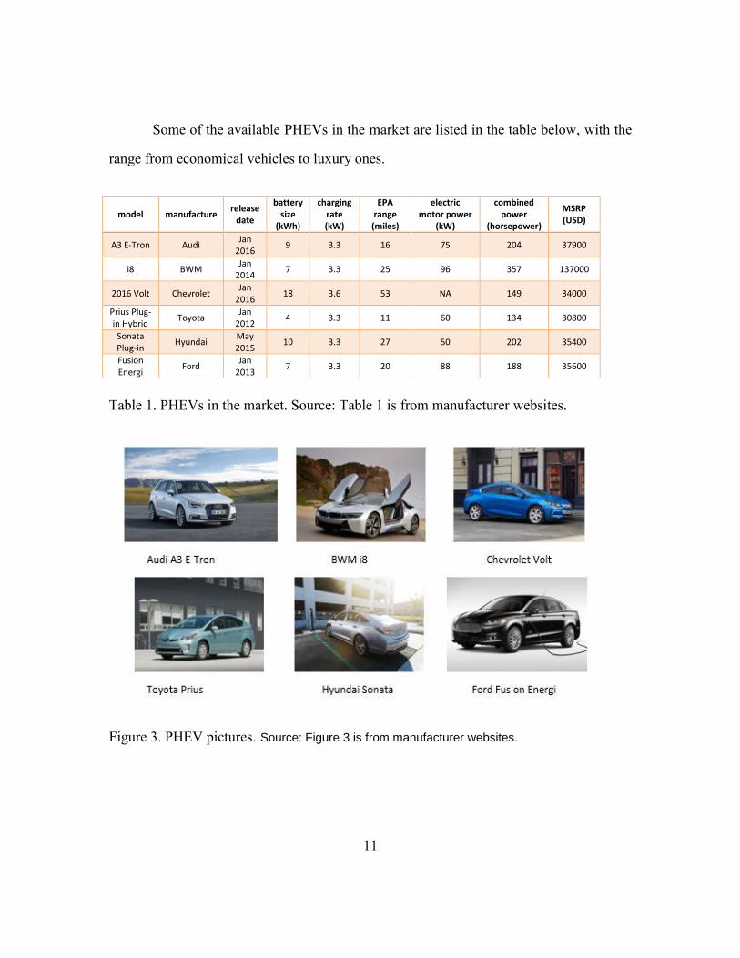
Some of the available PHEVs in the market are listed in the table below, with the
range from economical vehicles to luxury ones.
model manufacture release
date
battery size
(kWh)
charging rate (kW)
EPA range (miles)
electric motor power
(kW)
combined power
(horsepower)
MSRP (USD)
A3 E-Tron Audi Jan
2016 9 3.3 16 75 204 37900
i8 BWM Jan
2014 7 3.3 25 96 357 137000
2016 Volt Chevrolet Jan
2016 18 3.6 53 NA 149 34000
Prius Plug-in Hybrid
Toyota Jan
2012 4 3.3 11 60 134 30800
Sonata Plug-in
Hyundai May 2015
10 3.3 27 50 202 35400
Fusion Energi
Ford Jan
2013 7 3.3 20 88 188 35600
Table 1. PHEVs in the market. Source: Table 1 is from manufacturer websites.
Figure 3. PHEV pictures. Source: Figure 3 is from manufacturer websites.
12
2.2.3 PHEV’s Power Interface
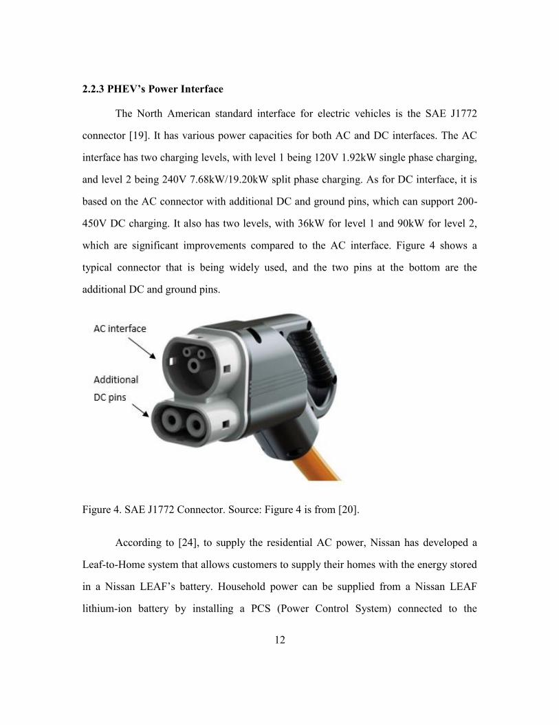
The North American standard interface for electric vehicles is the SAE J1772
connector [19]. It has various power capacities for both AC and DC interfaces. The AC
interface has two charging levels, with level 1 being 120V 1.92kW single phase charging,
and level 2 being 240V 7.68kW/19.20kW split phase charging. As for DC interface, it is
based on the AC connector with additional DC and ground pins, which can support 200-
450V DC charging. It also has two levels, with 36kW for level 1 and 90kW for level 2,
which are significant improvements compared to the AC interface. Figure 4 shows a
typical connector that is being widely used, and the two pins at the bottom are the
additional DC and ground pins.
Figure 4. SAE J1772 Connector. Source: Figure 4 is from [20].
According to [24], to supply the residential AC power, Nissan has developed a
Leaf-to-Home system that allows customers to supply their homes with the energy stored
in a Nissan LEAF’s battery. Household power can be supplied from a Nissan LEAF
lithium-ion battery by installing a PCS (Power Control System) connected to the

13
household’s distribution board. The PCS handles the power conversion and control of the
amount of power supply. Other car models such as Mitsubishi Outlander and Toyota
Prius also have the feature of Vehicle-to-Home discharging.
2.3 PHOTOVOLTAIC PANELS
2.3.1 Panel Model
A solar panel can convert incident sunlight into electricity by photovoltaic
conversion. Each individual cell in the panel is a large-scale semiconductor diode that
allows light to penetrate into the p-n junction region. Photons are absorbed in the
junction, generating excess electrons and holes. When the electrons flow through an
external circuit, then power is produced.
In [21], the PV module is modeled as the equivalent circuit below, where the cell
is equivalent to a current source in parallel with a diode and a shunt resistor, together
with a series resistor. The series resistance represents the internal resistance depending on
the p-n junction depth, the impurities and the contact resistance. The shunt resistance
conducts the leakage current to ground.
Figure 5. Equivalent circuit of a PV module. Source: This figure is from [21]

14
From the circuit, the output current can be represented as
𝐼 = 𝐼𝑝ℎ − 𝐼𝐷 − 𝐼𝑠ℎ … (2.1)
where the shunt current is
𝐼𝑠ℎ =𝑉𝑠ℎ
𝑅𝑠ℎ=
𝑈 + 𝐼 ∙ 𝑅𝑠
𝑅𝑠ℎ… (2.2)
The diode current is given by the Shockley diode equation as
𝐼𝐷 = 𝐼𝑠 ∙ (𝑒𝑉𝐷
𝑛∙𝑉𝑇 − 1) … (2.3)
Where:
• Is is the reverse bias saturation current.
• VD is forward voltage across diode, which is also 𝑈 + 𝐼 ∙ 𝑅𝑠.
• VT is the thermal voltage, and
• n is the ideality factor.
By the approximation of ignoring leakage current, a simplified PV panel output I-
V equation can be derived as
𝐼 = 𝐼𝑝ℎ − 𝐴(𝑒𝐵∙𝑈 − 1) … (2.4)
where Iph, A and B are the panel parameters that vary with panel characteristic
and solar radiation. With measurements taken over the rooftop PVs on ECJ, UT Austin
for a particular illumination level, the corresponding current and power against voltage
curve is shown in Figure 6:
15
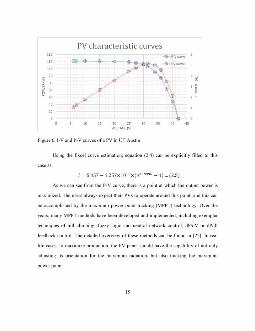
Figure 6. I-V and P-V curves of a PV in UT Austin
Using the Excel curve estimation, equation (2.4) can be explicitly filled to this
case as
𝐼 = 5.457 − 1.257×10⁻³×(𝑒0.1999𝑈 − 1) … (2.5)
As we can see from the P-V curve, there is a point at which the output power is
maximized. The users always expect their PVs to operate around this point, and this can
be accomplished by the maximum power point tracking (MPPT) technology. Over the
years, many MPPT methods have been developed and implemented, including exemplar
techniques of hill climbing, fuzzy logic and neutral network control, dP/dV or dP/dI
feedback control. The detailed overview of these methods can be found in [22]. In real
life cases, to maximize production, the PV panel should have the capability of not only
adjusting its orientation for the maximum radiation, but also tracking the maximum
power point.
0
1
2
3
4
5
6
0
20
40
60
80
100
120
140
160
180
0 5 10 15 20 25 30 35 40 45
CU
RR
ENT
(A)
PO
IWER
(W
)
VOLTAGE (V)
PV characteristic curvesP-V curve
I-V curve
16
2.3.2 Panel Power Inverter
The PV panel requires a solar inverter to convert a variable DC power into a fixed
frequency AC power. Normally, if a PV feeds power back to the grid, then we need a grid
tied inverter, which has the function of phase matching and quick disconnection when the
grid shuts down; if a PV is used in an isolated system, an ordinary stand-alone inverter
can manage the power conversion.
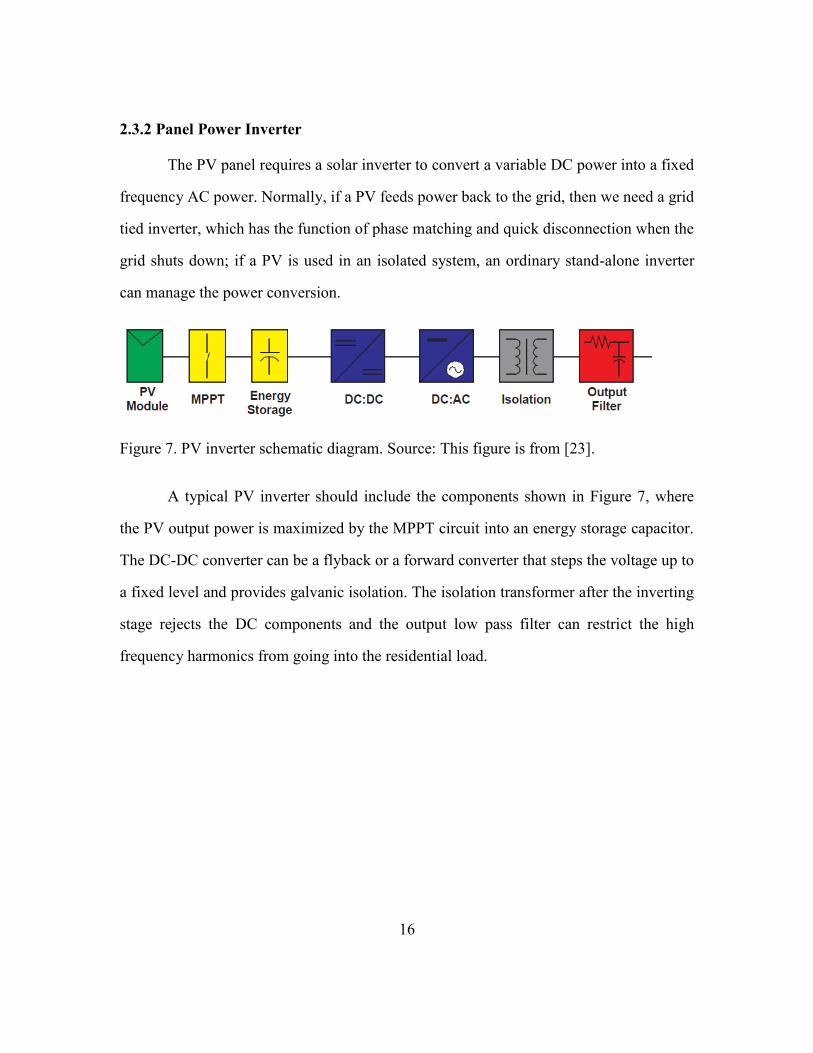
Figure 7. PV inverter schematic diagram. Source: This figure is from [23].
A typical PV inverter should include the components shown in Figure 7, where
the PV output power is maximized by the MPPT circuit into an energy storage capacitor.
The DC-DC converter can be a flyback or a forward converter that steps the voltage up to
a fixed level and provides galvanic isolation. The isolation transformer after the inverting
stage rejects the DC components and the output low pass filter can restrict the high
frequency harmonics from going into the residential load.
17
Chapter 3 Simulations of a V2H System
3.1 INTRODUCTION
With the V2H microgrid described in the previous chapters, it is still not
guaranteed that the system can operate in island mode for a period that is considered as
acceptable to customers. In this chapter, a particular scenario is set up for the microgrid
with the AC distribution system, and the simulation of the microgrid power backup event
in a whole year will be done. Based on the simulation, it can be determined if the V2H
system is feasible in a real-life case. The results will also be used later for comparison
with the DC distribution system.
3.2 SYSTEM MODEL
3.2.1 Load and PV Profile
The load and PV generation data were collected by Pecan Street Inc. in Austin.
These data were taken from 20 houses at 1-minute intervals over the whole year of 2012.
In this work, only one house’s profile was randomly chosen and this profile will also be
used in the DC distribution simulations in the following chapters. The PV profile is the
PV power measured at the load side, which means that the PV inverter efficiency has
been included. Therefore, the net load can be obtained by direct subtraction of load and
PV power. One assumption in the simulation is that the PV and load power measured is
the average power during the 1-minute interval.
3.2.2 Scenario Description
The simulation scenario is based on the research from [7], where the V2H system
is isolated from the utility grid. A power backup is the process of using the PHEV

18
generator and PV to supply the load during a grid outage. The details are specifically
introduced below:
1. Backup starting time: throughout the whole year, which is from day 1 to day 350
at 12 a.m., corresponding to minute 1,440 to minute 504,000 in the PV and load
profile. The reason for skipping the last couple of days in the year is that there
will not be enough data to support the simulation if the backup duration is longer
than the remaining days in this year.
2. Conversion efficiency: 88%, which means that there is a 12% one-way energy
loss when the battery is charged by the PV or discharges to serve the load.
3. Gasoline generator: at 1700rpm, the energy conversion ratio is 8.4kWh/gallon,
which means one gallon of fuel is converted to 8.4kWh of electric energy in the
battery. The initial gasoline in the tank is set at 17 gallons.
4. Battery: the battery size is 10.5kWh, with battery charge power of 12.4kW at
1700rpm. The maximum battery output power is 110kW, which can guarantee the
load to be supplied. The battery is assumed to be fully charged initially.
5. Backup duration: when there is no gasoline and the battery charge is below a
certain level (10%), the simulation ends, the total operation time is the backup
duration.
3.2.3 Simulation Scheme
We run the backup process for every possible backup staring time and plot the
backup duration against time, which means that the simulation should be repeated 350
times. Assuming when battery state of charge (SoC) is below 10%, the vehicle engine
charges the battery to 90% SoC, since charging battery to no more than 90% can help
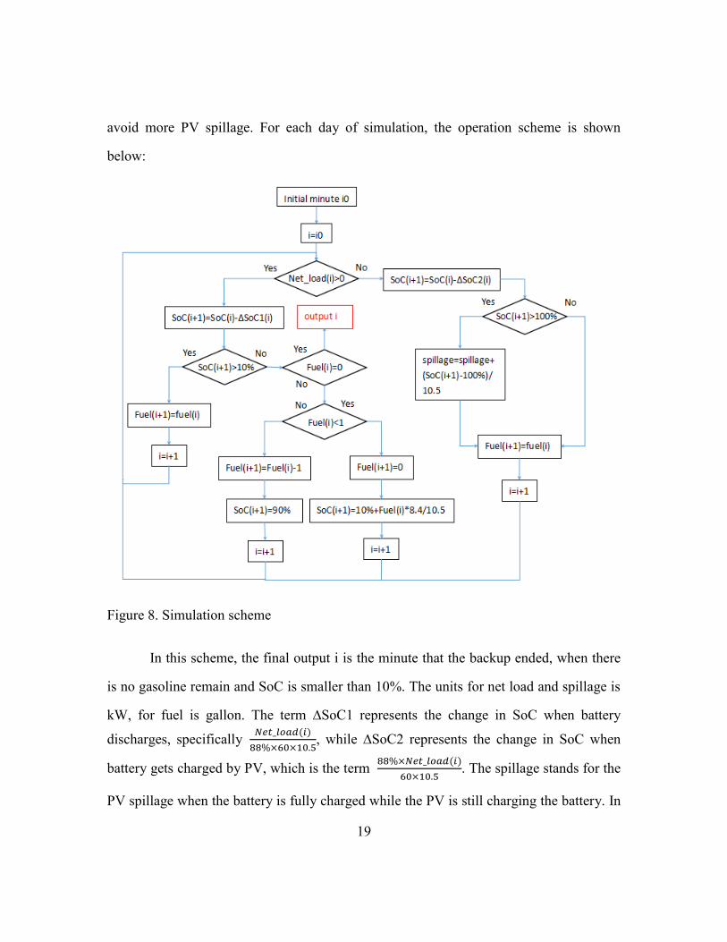
19
avoid more PV spillage. For each day of simulation, the operation scheme is shown
below:
Figure 8. Simulation scheme
In this scheme, the final output i is the minute that the backup ended, when there
is no gasoline remain and SoC is smaller than 10%. The units for net load and spillage is
kW, for fuel is gallon. The term ∆SoC1 represents the change in SoC when battery
discharges, specifically 𝑁𝑒𝑡_𝑙𝑜𝑎𝑑(𝑖)
88%×60×10.5, while ∆SoC2 represents the change in SoC when
battery gets charged by PV, which is the term 88%×𝑁𝑒𝑡_𝑙𝑜𝑎𝑑(𝑖)
60×10.5. The spillage stands for the
PV spillage when the battery is fully charged while the PV is still charging the battery. In

20
the judgement “Fuel(i) < 1”, “1” represents the fuel needed to charge the battery from
10% to 90%, since 80%×10.5
8.4= 1 (𝑔𝑎l𝑙𝑜𝑛).
3.3 SIMULATION RESULTS
3.3.1 Backup Duration
The duration of the microgrid power backup is dependent on the start of the grid
power outage. The figure below shows the backup duration against outage start date.
Figure 9. V2H backup duration throughout a year
From the simulation result, it can be concluded that the duration is relatively short
between day 150 and day 250, which is approximately the time of summer. The shorter
backup is expected in summer because normally load peaks occur during this season. The
shortest backup time is roughly 100 hours, which is still typically enough time for the
grid to recover from outage.
0
100
200
300
400
500
600
700
800
0 50 100 150 200 250 300 350
du
rati
on
(h
ou
r)
outage start time (day)
Backup duration in a year
21
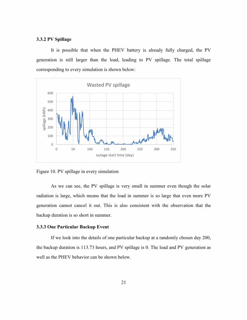
3.3.2 PV Spillage
It is possible that when the PHEV battery is already fully charged, the PV
generation is still larger than the load, leading to PV spillage. The total spillage
corresponding to every simulation is shown below:
Figure 10. PV spillage in every simulation
As we can see, the PV spillage is very small in summer even though the solar
radiation is large, which means that the load in summer is so large that even more PV
generation cannot cancel it out. This is also consistent with the observation that the
backup duration is so short in summer.
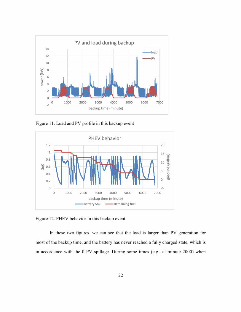
3.3.3 One Particular Backup Event
If we look into the details of one particular backup at a randomly chosen day 200,
the backup duration is 113.73 hours, and PV spillage is 0. The load and PV generation as
well as the PHEV behavior can be shown below.
0
100
200
300
400
500
600
0 50 100 150 200 250 300 350
spill
age
(kW
h)
outage start time (day)
Wasted PV spillage
22
Figure 11. Load and PV profile in this backup event
Figure 12. PHEV behavior in this backup event
In these two figures, we can see that the load is larger than PV generation for
most of the backup time, and the battery has never reached a fully charged state, which is
in accordance with the 0 PV spillage. During some times (e.g., at minute 2000) when
-2
0
2
4
6
8
10
12
14
0 1000 2000 3000 4000 5000 6000 7000
po
wer
(kW
)
backup time (minute)
PV and load during backup
load
PV
-5
0
5
10
15
20
0
0.2
0.4
0.6
0.8
1
1.2
0 1000 2000 3000 4000 5000 6000 7000
gaso
line
(gal
lon
)
SoC
backup time (minute)
PHEV behavior
Battery SoC Remaining fuel

23
gasoline is not being consumed, the battery SoC still goes up, which is because of the
charge from PV exceeding load.
From all the simulations above, a conclusion can be drawn that theoretically, the
V2H microgrid is capable of supporting a residential load for a significant amount of time
can be drawn.
24
Chapter 4 Power Electronics Interfaces in V2H System
4.1 INTRODUCTION
As was introduced in previous chapters, the configuration of a V2H microgrid has
two distributed generation units: PV panel and PHEV generator. A lot of DC/DC and
DC/AC conversion processes are taking place during an operation of the microgrid.
Therefore, the power electronics modules are very important in building a microgrid.
In this chapter, the power electronics interfaces in both a DC and AC microgrid
will be introduced, along with some basic power converter models such as rectifier,
inverter and DC/DC converter.
4.2 INTERFACES IN DC AND AC MICROGRID CONFIGURATION
There are two possible configurations of a microgrid: one is with an AC
distribution system, where both PV and battery energy are converted to AC first to flow
in the house; the other is a DC microgrid, where loads are classified and power is
distributed along a DC bus.
4.2.1 AC Distribution Microgrid
The first scenario is a typical Vehicle to Home (V2H) microgrid described in [7].
Under the assumption that one cannot drive the vehicle to fueling station during the
backup and the load demand remains normal, the operation can be simulated with a given
amount of gasoline and battery state of charge (SoC). The backup duration optimization
can become a complicated problem when taking the gasoline generator efficiency, battery
charging/discharging efficiency, PV generation, and loadshape into consideration. Figure
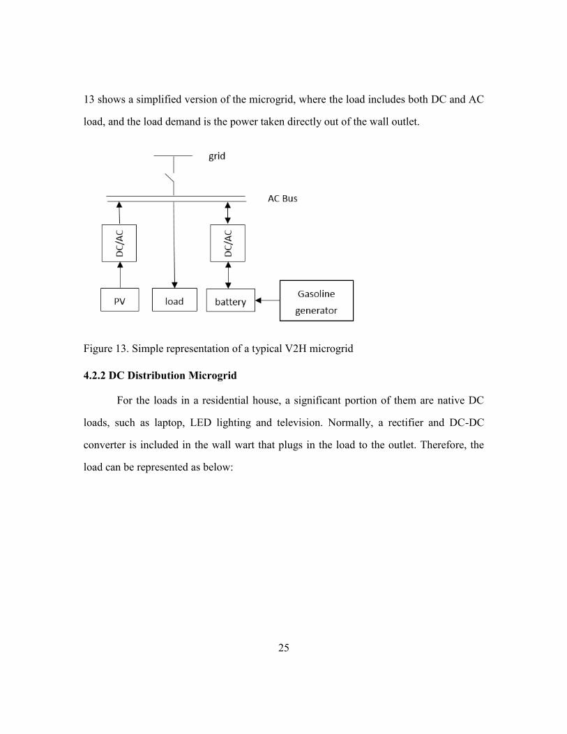
25
13 shows a simplified version of the microgrid, where the load includes both DC and AC
load, and the load demand is the power taken directly out of the wall outlet.
Figure 13. Simple representation of a typical V2H microgrid
4.2.2 DC Distribution Microgrid
For the loads in a residential house, a significant portion of them are native DC
loads, such as laptop, LED lighting and television. Normally, a rectifier and DC-DC
converter is included in the wall wart that plugs in the load to the outlet. Therefore, the
load can be represented as below:
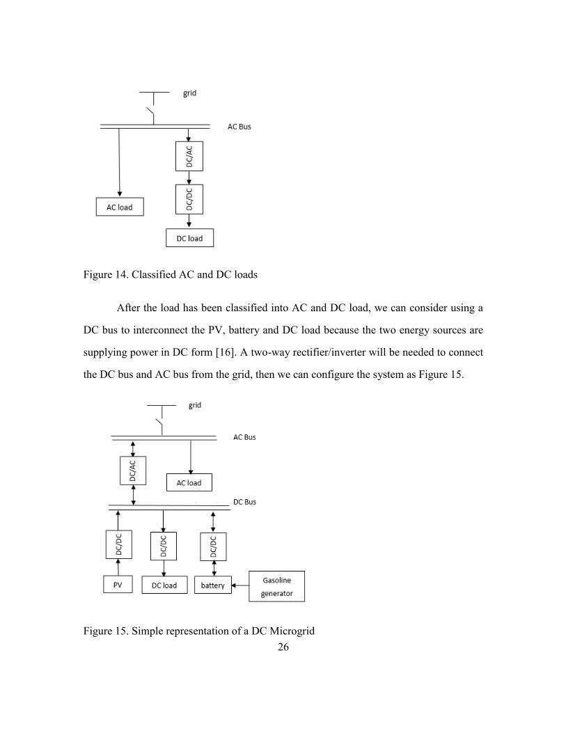
26
Figure 14. Classified AC and DC loads
After the load has been classified into AC and DC load, we can consider using a
DC bus to interconnect the PV, battery and DC load because the two energy sources are
supplying power in DC form [16]. A two-way rectifier/inverter will be needed to connect
the DC bus and AC bus from the grid, then we can configure the system as Figure 15.
Figure 15. Simple representation of a DC Microgrid
27
4.2.3 Comparisons between DC and AC Configurations
The utility grids are using an AC system as a convention mainly because the
power is generated in AC form and can be transmitted at high voltage using transformers.
However, microgrid does not have these features. In this V2H system, the distributed
generation units are DC in nature and power is not required to transmit at higher voltages
to lower loss. Thus, it is worth comparing the two distribution systems.
The AC system configuration is less complicated. The DG units are connected to
the distribution bus using DC/AC inverters and everything else is the same as the current
in-house power distribution system. The set-up of DC configuration is more challenging
because:
• Load classification is required to separate AC and DC loads
• An additional DC bus is added to serve the DC loads.
• Most appliance manufactures provide AC power adapters only. And
• there is a lack of standard for the DC bus and DC adapters.
However, there are more potential power losses in an AC configuration. The DC
power generation must be converted to AC to flow in the system, then converted back to
DC for consumption in these cases:
• When PV is used to charge PHEV battery, and
• when the power from battery and/or PV are used to serve DC load.
Overall, determining whether DC or AC microgrid is better for a house-level
configuration is complicated and many trade-offs need to be considered based on aspects
such as proportion of DC load, PV generation, difficulty of reconfiguration and on.

28
4.3 DC/DC CONVERTER MODELS
4.3.1 Buck Converter
A buck converter is used to step a DC voltage down. In a DC microgrid, the DC
bus is usually a high voltage bus. When using the DC bus to serve the DC load, for
example, an LED light bulb with a 12V rating, a buck converter or a similar step down
converter is needed to lower the voltage level.
4.3.1.1 Circuit Topology
Suppose there is a power MOSFET that keeps switching on and off with a period
of T and duty cycle of D. A constant input voltage level will be chopped to a rectangular
waveform. This process can be represented in Figure 16.
Figure 16. Input and output voltage from a switching MOSFET
When we look at the Fourier series of the output waveform, it will consist of a DC
average bias and a series of sinusoidal waveforms. For example, when the duty cycle
D=0.5, the Fourier series of the output square wave will be
𝑉𝑜𝑢𝑡(𝑡) = 𝑉𝐷𝐶−𝑏𝑖𝑎𝑠 +4
𝜋∑
1
𝑛sin (
𝑛𝜋𝑡
𝑇)
∞
𝑛=1,3,5…
… (4.1)
However, this amount of harmonics is definitely not acceptable for a microgrid
system. By applying an LC low pass filter at the output and adding a free-wheeling diode
to allow current flow when the switch is off, a basic buck converter topology is built up.

29
Figure 17. Topology of a basic buck converter. Source: Figure 17 is from [25]
The LC low pass filter will attenuate the output harmonics and make 𝑉𝑜𝑢𝑡 =
𝑉𝐷𝐶−𝑏𝑖𝑎𝑠 . Since the DC bias is the average of the rectangular wave, we have this
relationship:
𝑉𝑜𝑢𝑡 = 𝐷𝑉𝑖𝑛 … (4.2)
By changing duty ratio D, we can change the output voltage to a desired value.
4.3.1.2 Buck Converter Simulation
A buck converter circuit model with a switching frequency of 10kHz has been
built in Multisim for simulation. In the first simulation, the input voltage is 30V. The duty
ratio D is changed from 0 to 0.8 with a step of 0.2. In the second simulation, the duty
ratio is kept constant at 0.5, but the load resistance is changed from 2.08Ω to 5.55Ω.

30
Figure 18. Simulation circuit of a buck converter
Figure 19. Output response to change in duty ratio
Figure 20. Output response to change in load
31
From the first simulation in Figure 19, we can see that the output and input satisfy
equation (4.2). When the duty ratio is changed, the response takes some time to become
stable and is very oscillatory with obvious overshoot. The second simulation in Figure 20
also shows a similar oscillatory response, but this time since the duty ratio is constant, the
output voltage goes back to 15V eventually. These responses are understandable because
the buck converter is operating in open-loop and there is no controller to modify its
characteristics.
4.3.2 Boost Converter
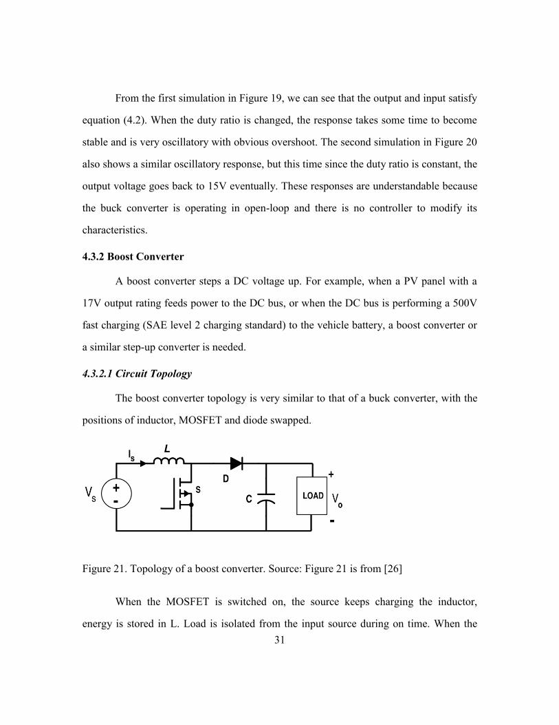
A boost converter steps a DC voltage up. For example, when a PV panel with a
17V output rating feeds power to the DC bus, or when the DC bus is performing a 500V
fast charging (SAE level 2 charging standard) to the vehicle battery, a boost converter or
a similar step-up converter is needed.
4.3.2.1 Circuit Topology
The boost converter topology is very similar to that of a buck converter, with the
positions of inductor, MOSFET and diode swapped.
Figure 21. Topology of a boost converter. Source: Figure 21 is from [26]
When the MOSFET is switched on, the source keeps charging the inductor,
energy is stored in L. Load is isolated from the input source during on time. When the

32
MOSFET is switched off, the energy stored in L is dumped into the load. This type of
converter is called indirect converter because the source does not directly serve the load.
Equation (4.3) shows the relationship between output voltage and input voltage. It
is derived by analyzing the current in inductor, and a detailed derivation can be found at
[27].
𝑉𝑜𝑢𝑡 =𝑉𝑖𝑛
1 − 𝐷… (4.3)
4.3.2.2 Boost Converter Simulation
A boost converter circuit model has been built from component rearrangement of
the buck converter. The MOSFET switching is still 10kHz. The input voltage is 10V. In
the first simulation, the duty ratio D is changed from 0 to 0.6 with a step of 0.2. The duty
ratio cannot be too close to 1 because it will make the output voltage too high. In the
second simulation, the duty ratio is kept constant at 0.4, but the load resistance is
suddenly changed from 2.08Ω to 5.55Ω.
Figure 22. Simulation circuit of a boost converter
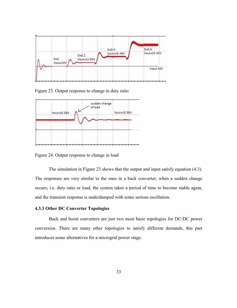
33
Figure 23. Output response to change in duty ratio
Figure 24. Output response to change in load
The simulation in Figure 23 shows that the output and input satisfy equation (4.3).
The responses are very similar to the ones in a buck converter, when a sudden change
occurs, i.e. duty ratio or load, the system takes a period of time to become stable again,
and the transient response is underdamped with some serious oscillation.
4.3.3 Other DC Converter Topologies
Buck and boost converters are just two most basic topologies for DC/DC power
conversion. There are many other topologies to satisfy different demands, this part
introduces some alternatives for a microgrid power stage.
34
4.3.3.1 Buck-Boost Converter
Figure 25. Topology of a buck-boost converter. Source: Figure 25 is from [26].
The buck-boost converter can either step up or step down a DC voltage. The user
can adjust its duty ratio to decide whether it will work in buck mode or boost mode.
However, its output voltage will be in reversed polarity of the input voltage.
4.3.3.2 Cuk Converter
Figure 26. Topology of a Cuk converter. Source: Figure 26 is from [26]
A Cuk converter also has an output voltage magnitude that can be either greater
than or less than the input voltage magnitude and has an inverting output. However, it
uses an additional set of inductor and capacitor compared to the buck-boost converter.
The more complicated design not only reduces harmonics because the inductor at the
input side acts as a filter, but also gives a continuous current at the input side, unlike the
discontinuous input current in a buck-boost converter.

35
4.3.3.3 Bi-directional Converter
Figure 27. Topology of a bi-directional converter. Source: Figure 27 is from [28]
Figure 27 shows a bi-directional converter with two terminals of E1 at 24V and E2
at 48V. When MOSFET Q2 is driven, power is flowing from E1 to E2, the circuit is
working as a boost converter. When MOSFET Q1 is driven, power is flowing from E2 to
E1, the circuit is working as a buck converter.
The bi-directional converter can be installed between the DC bus and the PHEV
battery, since the power flow can be in either direction depending on if the battery is
charged by PV or discharges to load.
4.4 DC/AC CONVERTER MODELS
4.4.1 Rectifier
A rectifier is used to convert AC power into DC power, for example, when the
AC bus is charging the PHEV battery in the AC microgrid. In the power adapters of some
electronic devices such as a laptop, there is a rectifier in the first power stage to convert
AC into DC, then step the DC voltage down to serve the device.
36
4.4.1.1 Circuit Model
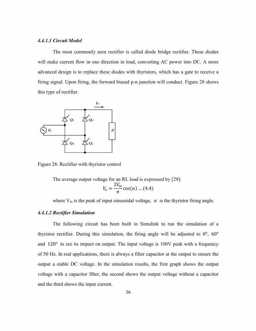
The most commonly seen rectifier is called diode bridge rectifier. These diodes
will make current flow in one direction in load, converting AC power into DC. A more
advanced design is to replace these diodes with thyristors, which has a gate to receive a
firing signal. Upon firing, the forward biased p-n junction will conduct. Figure 28 shows
this type of rectifier.
Figure 28. Rectifier with thyristor control
The average output voltage for an RL load is expressed by [29]:
𝑉𝑜 =2𝑉𝑚
𝜋cos(𝛼) … (4.4)
where Vm is the peak of input sinusoidal voltage, 𝛼 is the thyristor firing angle.
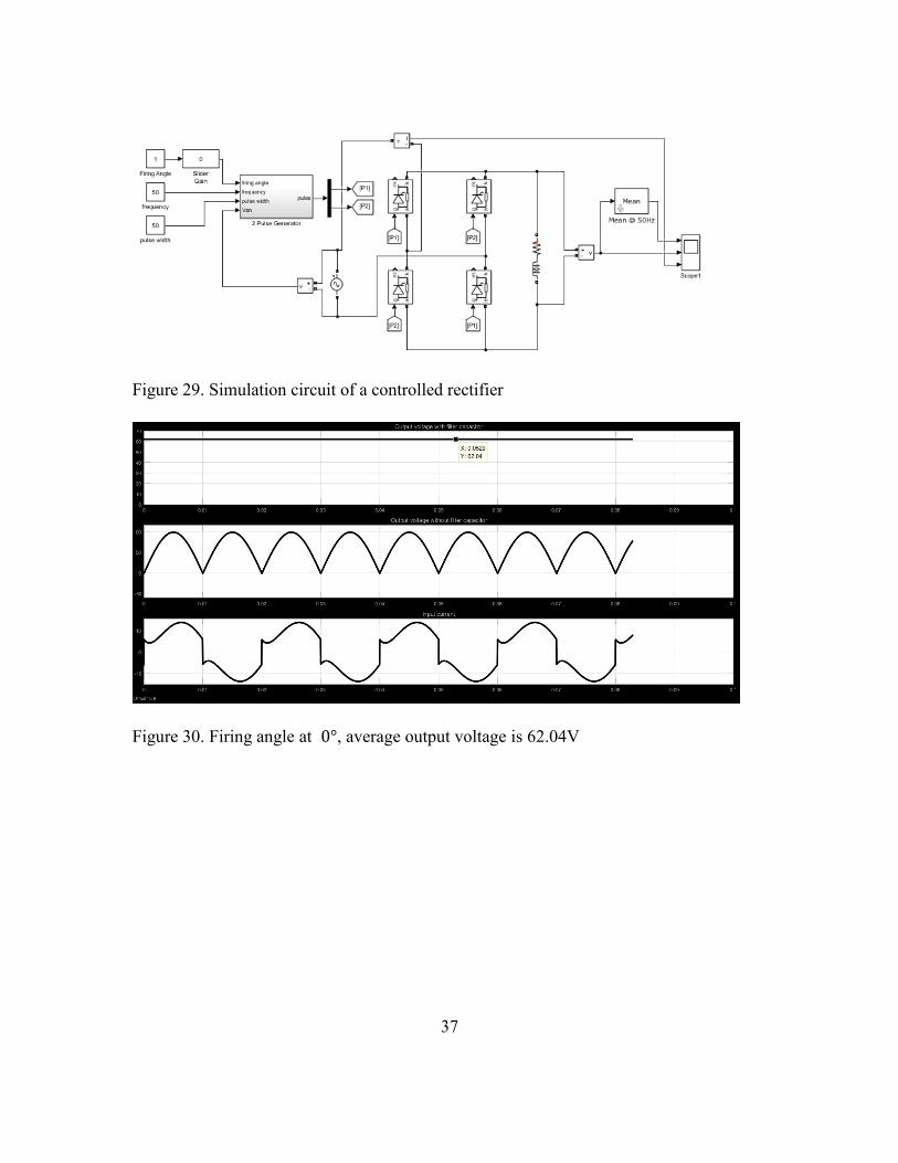
4.4.1.2 Rectifier Simulation
The following circuit has been built in Simulink to run the simulation of a
thyristor rectifier. During this simulation, the firing angle will be adjusted to 0°, 60°
and 120° to see its impact on output. The input voltage is 100V peak with a frequency
of 50 Hz. In real applications, there is always a filter capacitor at the output to ensure the
output a stable DC voltage. In the simulation results, the first graph shows the output
voltage with a capacitor filter, the second shows the output voltage without a capacitor
and the third shows the input current.
37
Figure 29. Simulation circuit of a controlled rectifier
Figure 30. Firing angle at 0°, average output voltage is 62.04V

38
Figure 31. Firing angle at 60°, average output voltage is 43.55V
Figure 32. Firing angle at 120°, average output voltage is 12.89V
From these simulations, we can see that the relationship between output voltage
and firing angle satisfies equation (4.4). Increasing the firing angle will bring the output
voltage down. It is worth noticing that the input current is highly nonlinear, therefore,
manufacturers should be very careful with their design because it will inject harmonics
39
pollutions as well as bringing the power factor down. A rectifier often has a built-in
harmonics filter and power factor correction (PFC) circuit.
4.4.2 Power Inverter
A power inverter is used to convert DC power into AC. In a microgrid system, the
PV and EV battery need inverters to serve the AC load. Because the application is in a
house-level microgrid not an industrial or commercial building, only single phase
inverters are investigated in this thesis.
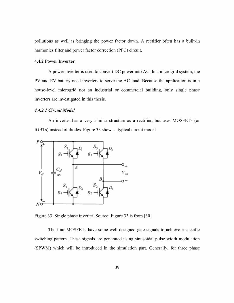
4.4.2.1 Circuit Model
An inverter has a very similar structure as a rectifier, but uses MOSFETs (or
IGBTs) instead of diodes. Figure 33 shows a typical circuit model.
Figure 33. Single phase inverter. Source: Figure 33 is from [30]
The four MOSFETs have some well-designed gate signals to achieve a specific
switching pattern. These signals are generated using sinusoidal pulse width modulation
(SPWM) which will be introduced in the simulation part. Generally, for three phase

40
inverters, the gate signals are generated using space vector pulse width modulation
(SVPWM); for single phase, signals come from SPWM.
The MOSFETs S1 to S4 will switch a pattern so that during some time, S1 and S2
are on, S3 and S4 are off, load current flows from A to B. Then S3 and S4 are on, S1 and
S2 are off, the current flows from B to A. This will create an AC load current. It is also
important to make sure that S1 and S4 are not switched on at the same time, as well as S2
and S3, so that the DC source is not shorted.
4.4.2.2 Inverter Simulation
The SPWM switching pattern has two types: unipolar and bipolar. The simulation
here uses unipolar switching, which compares a triangular wave with carrier frequency fc
and two sinusoidal waves in reversed phase with modulation frequency fm. The inverter
output voltage VAB = VAN – VBN switches either between zero and +Vd during positive
half cycle or between zero and –Vd during negative half cycle of the fundamental
frequency, thus this scheme is called unipolar modulation. The modulation index ma is
defined as
𝑚𝑎 =max |𝑉𝑚|
max |𝑉𝑐𝑟|… (4.5)
41
Figure 34. Waveforms of unipolar SPWM. Source: Figure 34 is from [30].
In our simulation, the carrier frequency fc = 4kHz and the modulation frequency
fm = 60Hz. The input voltage Vd is 50V and the modulation index ma = 0.8. Figure 35 and
36 shows the output voltage VAB and its frequency analysis.

42
Figure 35. Output voltage VAB
Figure 36. Spectrum analysis of output VAB
From Figure 35, it can be seen that VAB follows the waveform in Figure 34, but
since it has a much higher carrier frequency (4kHz) compared to the modulation
frequency (60Hz), the pulses look much denser. At frequency domain, the first harmonic
43
is at approximately 4kHz with an amplitude of 10.6V, which means that a low pass filter
with a cut-off frequency less than 4kHz is required. The spectrum analysis shows the
advantage of using PWM to generate transistor gate signals: the harmonics have very
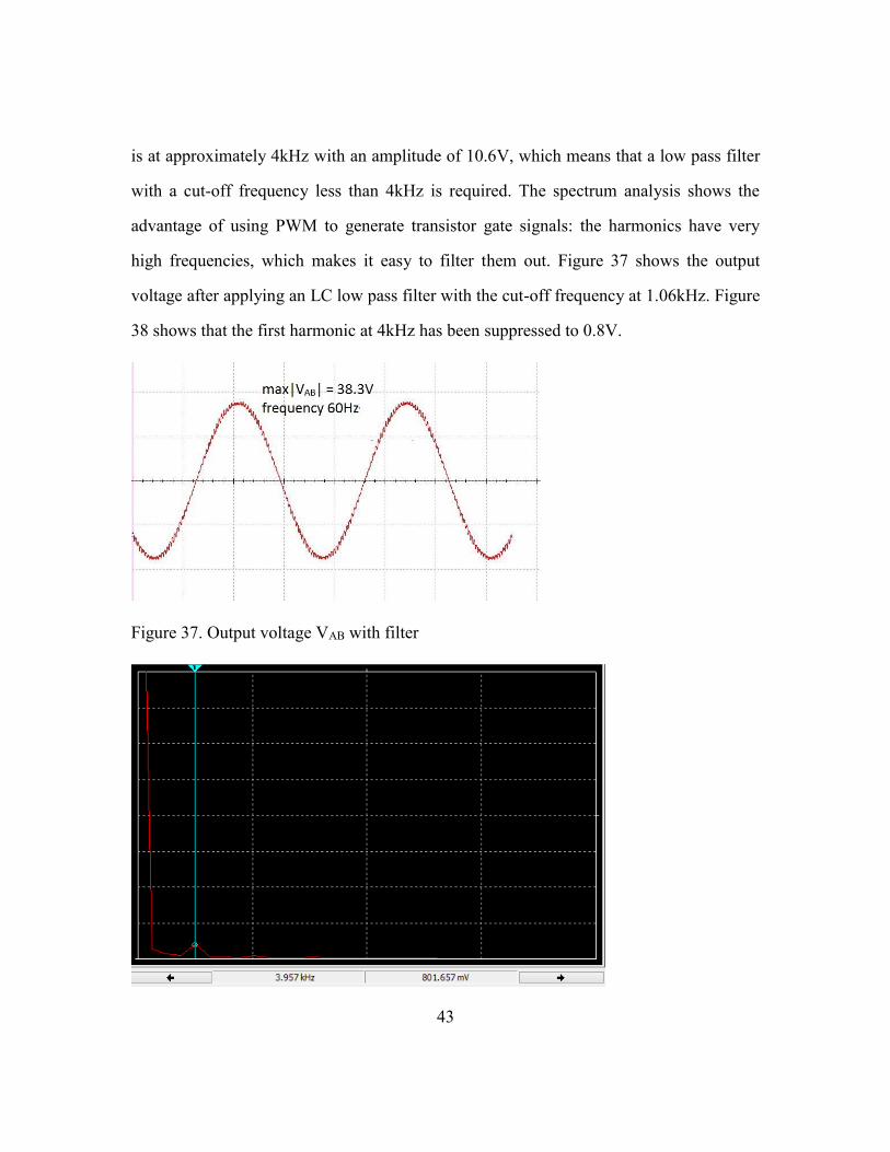
high frequencies, which makes it easy to filter them out. Figure 37 shows the output
voltage after applying an LC low pass filter with the cut-off frequency at 1.06kHz. Figure
38 shows that the first harmonic at 4kHz has been suppressed to 0.8V.
Figure 37. Output voltage VAB with filter

44
Figure 38. Spectrum analysis of output VAB with filter
The output voltage after the filter is expected to be
max |𝑉𝐴𝐵| = 𝑚𝑎 ∙ 𝑉𝑑 = 0.8 ∙ 50 = 40𝑉 … (4.6)
However, the actual voltage is slightly lower than 40V in Figure 37. This is
because that dead time is inserted to make sure that two switches on the same leg do not
switch on at the same time. During the deadtime, all four switches are off, the power flow
from DC to AC is cut off. The dead time insertion will result in some voltage magnitude
loss. From the results, we can see that the inverter has successfully converted a DC
voltage into a sinusoidal AC. The output voltage can be adjusted by changing the
modulation index. In a real power system, a phase locked loop is required to make sure
that the connection from a DC generation to an AC bus has the same phase as the
distribution line.

45
Chapter 5 Power Electronics Control in V2H System
5.1 INTRODUCTION
In a microgrid system, there are lots of voltage changes taking place in a house
load. For example, when we are using a DC bus to charge a Lithium battery in the
customer load, the charging voltage does not stay constant. Figure 39 shows a Li-ion
battery charging profile:
Figure 39. Charging profile of a Li-ion battery. Source: Figure 39 is from [31]
During the charging process, the voltage slowly rises to 4.1V, then stays constant,
and fluctuates after it finishes charging.
From the DC/DC converter parts in Chapter 4, we know that in order to change
the output voltage, the MOSFET duty ratio needs be changed. However, from the
simulations results, it is shown that the transients during a voltage change is very

46
unacceptable. In this chapter, we will seek the method to change the highly oscillatory
transients to a fast and smooth response.
5.2 INTRODUCTION TO FREQUENCY COMPENSATION
In a feedback control system, a compensator is used to improve an undesirable
frequency response. The whole closed-loop feedback control system block diagram is
shown in Figure 40.
Figure 40. Closed-loop block diagram
Take the following system transfer function for example:
𝐺(𝑠) =40
𝑠2 + 2𝑠… (5.1)
The Bode plot of this system is shown in Figure 41:
47
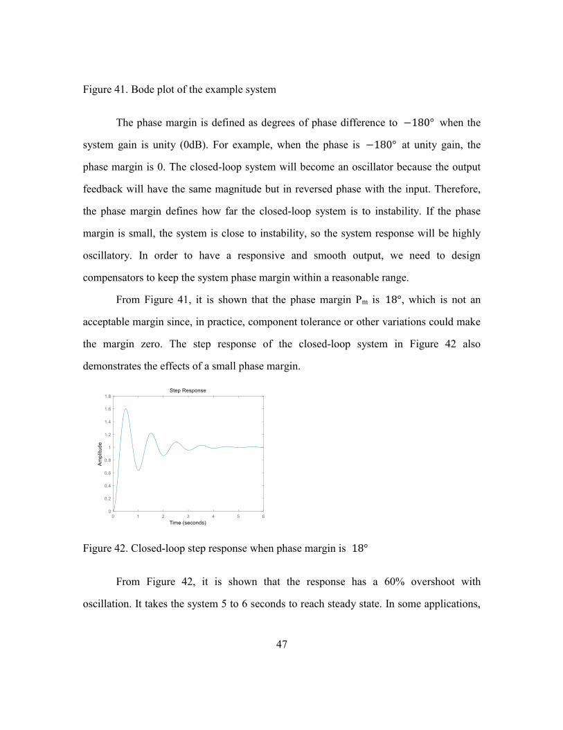
Figure 41. Bode plot of the example system
The phase margin is defined as degrees of phase difference to −180° when the
system gain is unity (0dB). For example, when the phase is −180° at unity gain, the
phase margin is 0. The closed-loop system will become an oscillator because the output
feedback will have the same magnitude but in reversed phase with the input. Therefore,
the phase margin defines how far the closed-loop system is to instability. If the phase
margin is small, the system is close to instability, so the system response will be highly
oscillatory. In order to have a responsive and smooth output, we need to design
compensators to keep the system phase margin within a reasonable range.
From Figure 41, it is shown that the phase margin Pm is 18°, which is not an
acceptable margin since, in practice, component tolerance or other variations could make
the margin zero. The step response of the closed-loop system in Figure 42 also
demonstrates the effects of a small phase margin.
Figure 42. Closed-loop step response when phase margin is 18°
From Figure 42, it is shown that the response has a 60% overshoot with
oscillation. It takes the system 5 to 6 seconds to reach steady state. In some applications,

48
a slow and oscillatory response like this is not acceptable. If the following compensator is
introduced:
𝐶(𝑠) = 4.2 ∙𝑠 + 4.35
𝑠 + 18.11… (5.2)
The Bode plot of the system with compensation is shown in Figure 43, with a
phase margin of 50.3°.
Figure 43. Bode plot comparison of system with and without compensation
From the Bode plot, it is shown that the phase margin has been boosted by a large
portion, from 18° to 50.3°. The frequency at which the system has unity gain, also
called crossover frequency, has shifted to the right. This indicates that the system can
respond to a higher frequency, thus is less immune to noise.
Figure 44 compares the two closed-loop step responses.
49
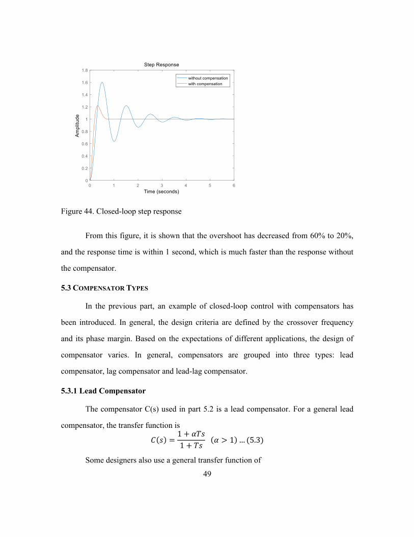
Figure 44. Closed-loop step response
From this figure, it is shown that the overshoot has decreased from 60% to 20%,
and the response time is within 1 second, which is much faster than the response without
the compensator.
5.3 COMPENSATOR TYPES
In the previous part, an example of closed-loop control with compensators has
been introduced. In general, the design criteria are defined by the crossover frequency
and its phase margin. Based on the expectations of different applications, the design of
compensator varies. In general, compensators are grouped into three types: lead
compensator, lag compensator and lead-lag compensator.
5.3.1 Lead Compensator
The compensator C(s) used in part 5.2 is a lead compensator. For a general lead
compensator, the transfer function is
𝐶(𝑠) =1 + 𝛼𝑇𝑠
1 + 𝑇𝑠 (𝛼 > 1) … (5.3)
Some designers also use a general transfer function of
50
𝐶(𝑠) = 𝐾𝑠 − 𝑧0
𝑠 − 𝑝0… (5.4)
These two representations are equivalent. (5.4) represents the transfer function in
terms of its gain, pole and zero. The gain 𝐾 = 𝛼, the pole 𝑝0 = −1
𝑇and the zero 𝑧0 =
−1
𝛼𝑇. Since 𝛼 > 1, the pole will be on the left of the zero. In the example compensator in
equation (5.2), the pole is at -18.11 rad/s and the zero is at -4.35 rad/s. So, the
corresponding 𝛼 = 4.2, 𝑇 = 0.055. The Bode plot of the compensator is shown as
Figure 45. Bode plot of the lead compensator
Figure 45 shows that the positive phase is added to the system between these two
frequencies. The maximum amount of phase is added at the center frequency, which is
calculated according to equation (5.5).
𝑤𝑚 =1
𝑇√𝛼… (5.5)
The 𝑤𝑚 here is calculated as 8.87 rad/s, which is the same as the frequency
shown in the plot. The maximum phase boost can be calculated by the equation below:
∅ = 𝑠𝑖𝑛−1 (𝛼 − 1
𝛼 + 1) … (5.6)
51
The ∅ here is calculated as 38°, which is very close to the 37.8° phase boost in
the plot. The process of designing a lead compensator is to determine 𝛼 from the phase
margin requirements, then determine T to place the added phase at a desired crossover
frequency.
It is also worth noticing that the gain at low frequency is kept unity, so the system
steady state response will not be affected much. However, the gain at high frequency has
been raised by the compensator. This will increase the system crossover frequency,
increase the transient response speed, but reduce noise immunity. These trade-offs need
to be considered in a design.
5.3.2 Lag Compensator
A lag compensator has an opposite impact to a lead compensator. The general
function for a lag compensator can be written as:
𝐶(𝑠) =1
𝛼(
1 + 𝛼𝑇𝑠
1 + 𝑇𝑠) (0 < 𝛼 < 1) … (5.7)
The transfer function can also be written in the form of equation (5.4), but with
the pole on the right of the zero. The main difference is that the lag compensator adds
negative phase to the system over the specified frequency range, while a lead
compensator adds positive phase.
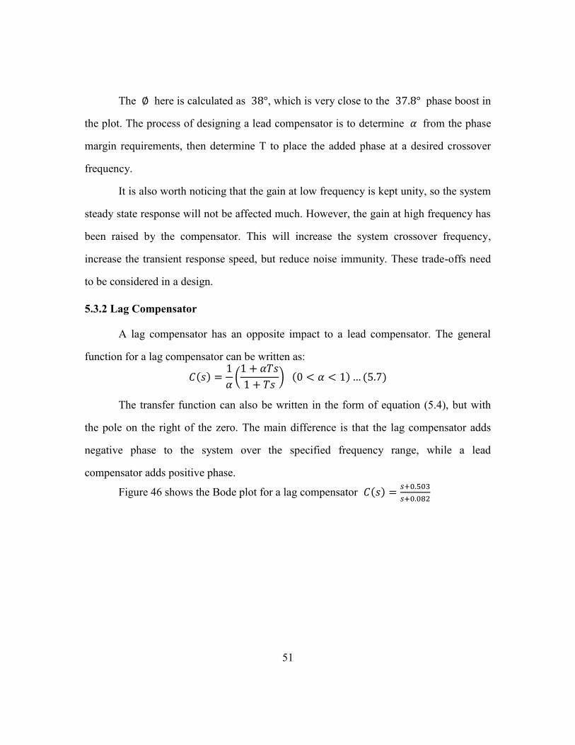
Figure 46 shows the Bode plot for a lag compensator 𝐶(𝑠) =𝑠+0.503
𝑠+0.082
52
Figure 46. Bode plot for a lag compensator
It can be confusing that since a higher phase margin gives a better response, what
is the reason to add a lag compensator to the system. In fact, the phase lag it brings is a
side effect of its benefits: to improve the system steady state response. From the
magnitude plot, the gain at low frequency is amplified by a factor of 1
𝛼 (0 < 𝛼 < 1),
leading to the reduction of steady state error (the error between output and reference input
when output stays constant) by a factor of 1
𝛼. The gain at high frequency is unity,
therefore the transient response time will not be impacted much.
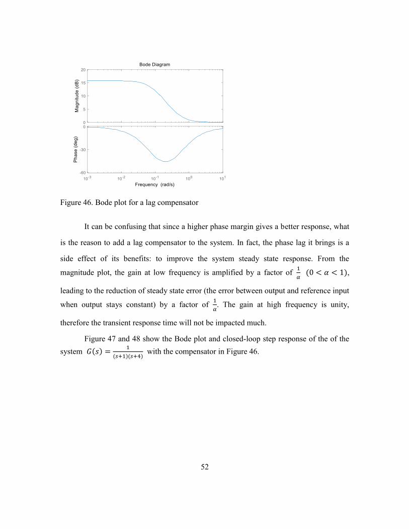
Figure 47 and 48 show the Bode plot and closed-loop step response of the of the
system 𝐺(𝑠) =1
(𝑠+1)(𝑠+4) with the compensator in Figure 46.
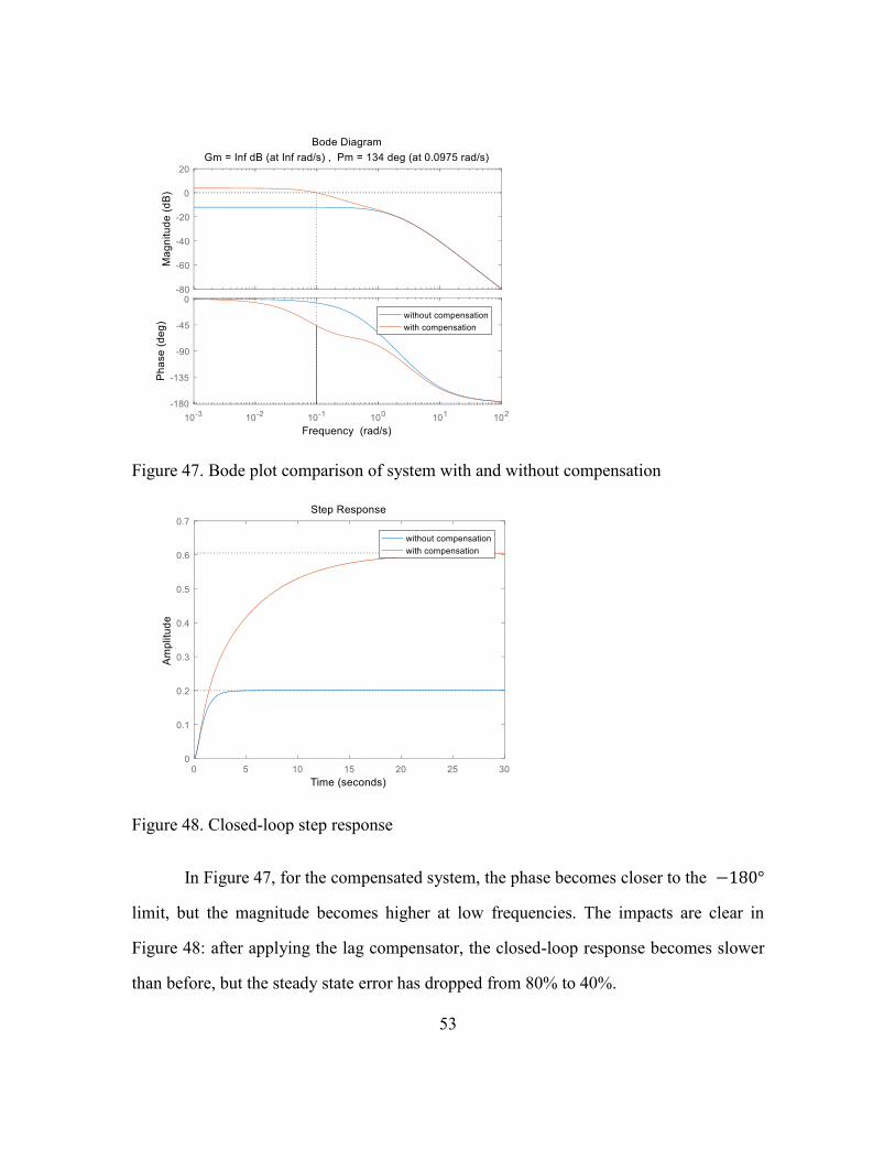
53
Figure 47. Bode plot comparison of system with and without compensation
Figure 48. Closed-loop step response
In Figure 47, for the compensated system, the phase becomes closer to the −180°
limit, but the magnitude becomes higher at low frequencies. The impacts are clear in
Figure 48: after applying the lag compensator, the closed-loop response becomes slower
than before, but the steady state error has dropped from 80% to 40%.
54
Overall, the trade-offs to consider in a lag compensator design is that the
potentially lowered phase margin will make system have a less satisfactory transient
response, become closer to instability, but have a smaller steady state error.
5.3.3 Lead-lag Compensator
In previous parts, the design rule introduced can be summarized as the following:
• To improve the system transient response, i.e. the phase margin, response time
and oscillations, we need a lead compensator.
• To improve the system steady state response, i.e. the steady state error, we need a
lag compensator.
However, in some applications, it is required to have not only a fast and smooth
transient response, but also a negligible steady state error. A lead-lag compensator is a
compensator that combines the advantages of both compensators. The general transfer
function of a lead-lag compensator can be expressed as:
𝐶(𝑠) = 𝐾1 + 𝑠𝑇1
1 + 𝛼𝑠𝑇1
1 + 𝑠𝑇2
1 + 𝛽𝑠𝑇2… (5.8)
where 𝛽 > 1, 0 < 𝛼 < 1, 𝑇1 < 𝑇2.
The Bode plot of an example lead-lag compensator 𝐶(𝑠) = 10(𝑠+100)(𝑠+0.1)
(𝑠+1000)(𝑠+0.01)is
shown in Figure 49:

55
Figure 49. Bode plot of a lead-lag compensator
In this figure, at low frequency, the lag compensator becomes effective to
improve the system steady state response; at high frequency, the lead compensator takes
over to improve the system transient response.
5.4 CONTROL APPLICATION IN POWER ELECTRONICS
The control block diagram for a voltage control mode DC/DC converter is shown
in Figure 50:
Figure 50. Closed-loop control of a DC/DC converter
The PWM simply converts the compensated error linearly into the duty cycle of
MOSFET gate-driving PWM signals. Thus, the converter transfer function and
compensator design need to be studied.

56
5.4.1 Converter Transfer Function
For different types of converters, the transfer function varies. In a general case,
the input voltage remains constant, so the transfer function is built between the input duty
cycle of MOSFET gate driver and the output voltage. Unlike the relationships given by
equation (4.2) and (4.3) where voltage and duty cycle are discussed in a sense of average,
to study the transient response, we need to look at the small signal model of the converter
due to the presence of a nonlinear MOSFET switch.
A buck converter will be studied in this part because it is most likely to supply
batteries, LEDs and other loads that require a varied voltage using a buck converter. The
circuit topology can be found at Figure 17:
Figure 17. Topology of a basic buck converter. Source: Figure 17 is from [25]
Suppose the duty ratio is D, input voltage is 𝑉𝑖𝑛, output voltage is 𝑉𝑜𝑢𝑡, output
current is 𝐼𝑜𝑢𝑡, inductor is L, capacitor is C, output is a resistor R, current through L is
𝐼𝐿 , current through C is 𝐼𝑐. The small signals are represented by lower case symbols.
When the switch is on at cycle D, there is this relationship:
𝐿𝑑𝐼𝐿
𝑑𝑡= 𝑉𝑖𝑛 − 𝑉𝑜𝑢𝑡 … (5.9)
And when switch is off at cycle (1-D), we have
𝐿𝑑𝐼𝐿
𝑑𝑡= −𝑉𝑜𝑢𝑡 … (5.10)
57
In average, the inductor current satisfies
𝐿𝑑𝐼𝐿
𝑑𝑡= 𝐷(𝑉𝑖𝑛 − 𝑉𝑜𝑢𝑡) + (1 − 𝐷)(−𝑉𝑜𝑢𝑡) = 𝐷𝑉𝑖𝑛 − 𝑉𝑜𝑢𝑡 … (5.11)
For the small signal inductor current:
𝐿𝑑(𝐼𝐿 + 𝑖𝐿)
𝑑𝑡= (𝐷 + 𝑑)(𝑉𝑖𝑛 + 𝑣𝑖𝑛) − (𝑉𝑜𝑢𝑡 + 𝑣𝑜𝑢𝑡)
= 𝐷𝑉𝑖𝑛 + 𝐷𝑣𝑖𝑛 + 𝑑𝑉𝑖𝑛 + 𝑑𝑣𝑖𝑛 − (𝑉𝑜𝑢𝑡 + 𝑣𝑜𝑢𝑡) … (5.12)
(5.12) – (5.11) gives
𝐿𝑑𝑖𝐿
𝑑𝑡= 𝐷𝑣𝑖𝑛 + 𝑑𝑉𝑖𝑛 + 𝑑𝑣𝑖𝑛 − 𝑣𝑜𝑢𝑡 … (5.13)
Since Vin is constant, its small signal 𝑣𝑖𝑛 → 0, (5.13) becomes
𝐿𝑑𝑖𝐿
𝑑𝑡= 𝑑𝑉𝑖𝑛 − 𝑣𝑜𝑢𝑡 … (5.14)
The small signal current in inductor satisfies
𝑖𝐿 =𝑣𝑜𝑢𝑡
𝑅+ 𝑖𝑐 =
𝑣𝑜𝑢𝑡
𝑅+ 𝐶
𝑑𝑣𝑜𝑢𝑡
𝑑𝑡… (5.15)
Plug (5.15) into (5.14) yields
𝐿
𝑅
𝑑𝑣𝑜𝑢𝑡
𝑑𝑡+ 𝐿𝐶
𝑑2𝑣𝑜𝑢𝑡
𝑑𝑡2= 𝑑𝑉𝑖𝑛 − 𝑣𝑜𝑢𝑡 … (5.16)
Assuming zero initial condition, and take the Laplace transform of (5.16) gives
(𝐿𝐶𝑠2 +𝐿
𝑅𝑠 + 1) 𝑣𝑜𝑢𝑡(𝑠) = 𝑑(𝑠)𝑉𝑖𝑛 … (5.17)
The transfer function G(s) then can be derived as
𝐺(𝑠) =𝑣𝑜𝑢𝑡(𝑠)
𝑑(𝑠)=
𝑉𝑖𝑛
(𝐿𝐶𝑠2 +𝐿𝑅 𝑠 + 1)
… (5.18)
This transfer function gives the transient relationship between a change in duty
cycle and the corresponding change in output voltage. Consider the following parameters:
𝑉𝑖𝑛 = 10𝑉, 𝐿 = 0.5𝑚𝐻, 𝐶 = 0.5𝑚𝐹, 𝑅 = 2𝛺.
The system becomes
𝐺(𝑠) =10
2.5×10⁻⁷𝑠2 + 2.5×10⁻⁵𝑠 + 1… (5.19)
58
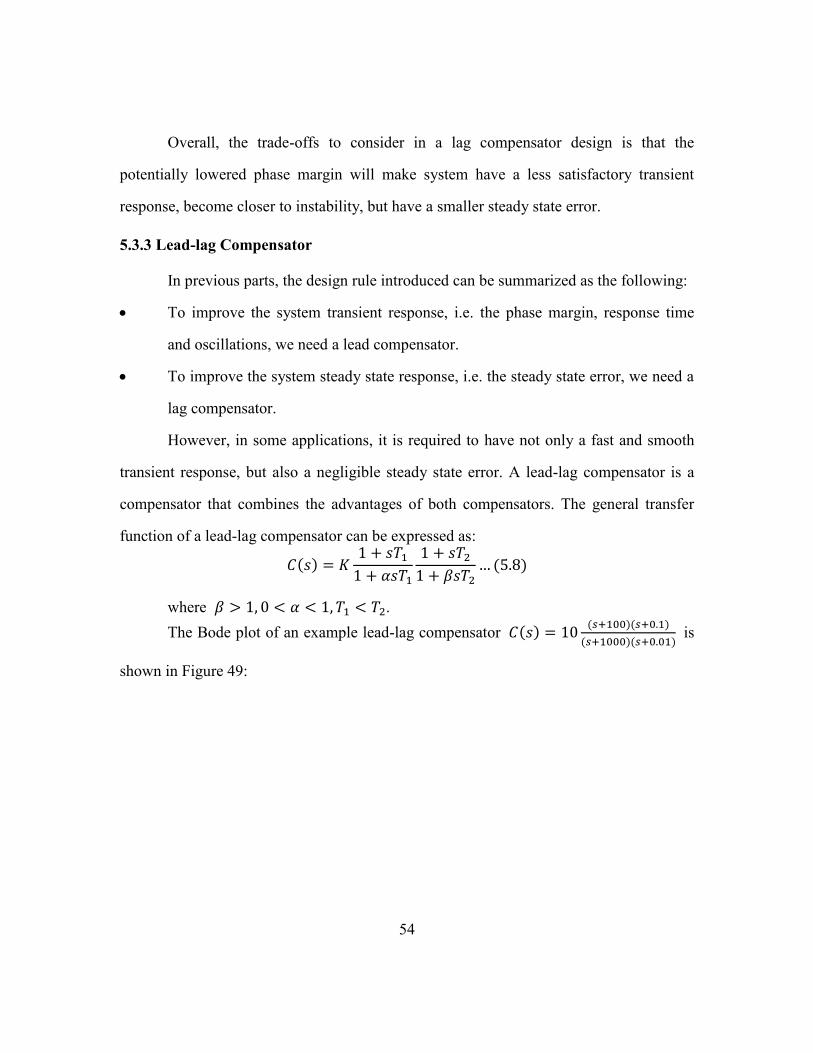
Figure 51 and 52 show the Bode plot and closed-loop step response of this buck
converter.
Figure 51. Bode plot of example buck converter
Figure 52. Closed-loop step response of example buck converter

59
The buck converter has a phase margin of 9.49° which has caused unacceptable
oscillation and an overshoot of 60%, the response time is roughly 0.01s which is good
enough, and the steady state error is 10%.
5.4.2 Lead-lag Compensator Design
First, we design a lead compensator to increase its phase margin. The crossover
frequency is at 6.7×10³ rad/s, and we add a 50° phase boost to the system. From
equation (5.6), 𝛼𝑙𝑒𝑎𝑑 can be calculated as 7.548. We inject the 50° phase boost at the
crossover frequency, however, since a lead compensator will increase the system
crossover frequency, it is better to put the phase boost at a higher frequency, for example
at 1×10⁴, then from equation (5.5), 𝑇𝑙𝑒𝑎𝑑can be calculated as 3.64×10⁻⁵. The lead
compensator is designed as
𝐶𝑙𝑒𝑎𝑑 =2.747×10⁻⁴𝑠 + 1
3.64×10⁻⁵𝑠 + 1… (5.20)
With the transient response improved, the next is the steady state response.
Suppose we decrease the steady state error by a factor of 7.548, so 1
𝛼𝑙𝑎𝑔= 7.548, 𝛼𝑙𝑎𝑔 =
0.132. Let 𝑇𝑙𝑒𝑎𝑑 = 0.002, so from equation (5.5), the phase lag will be injected at 1374
rad/s. Since in the original system, the phase margin at this frequency is very robust, the
design of lag compensator is reasonable. The transfer function is written as
𝐶𝑙𝑎𝑔 =2.64×10⁻⁴𝑠 + 1
2.64×10⁻⁴𝑠 + 0.132… (5.21)
Then the lead-lag compensator can be written as
𝐶𝑙𝑒𝑎𝑑−𝑙𝑎𝑔 = 𝐶𝑙𝑒𝑎𝑑𝐶𝑙𝑎𝑔 … (5.22)
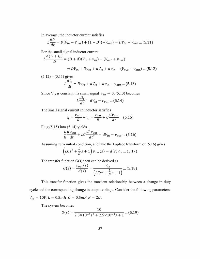
Figure 53 shows the frequency response of this compensator:
60
Figure 53. Bode plot of the lead-lag compensator
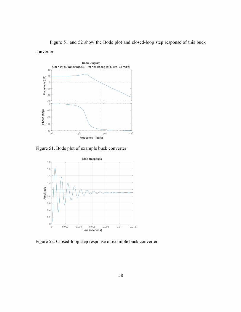
5.4.3 Buck Converter Closed-loop Simulation
Suppose the duty cycle of the buck converter is 0.5, therefore the output voltage is
5V. A step input in reference voltage means that the reference voltage is increase from
5V to 6V, and the output voltage will follow the reference to increase in a closed-loop.
Figure 54 compares the frequency response to the original system without compensation.
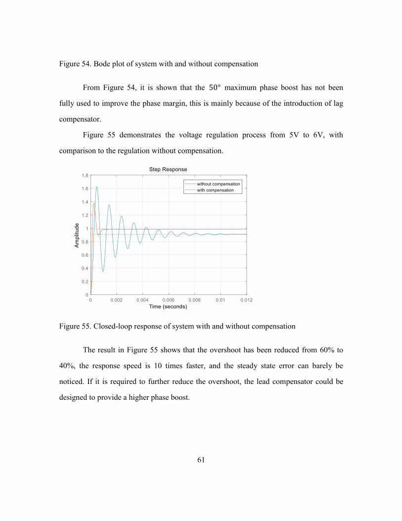
61
Figure 54. Bode plot of system with and without compensation
From Figure 54, it is shown that the 50° maximum phase boost has not been
fully used to improve the phase margin, this is mainly because of the introduction of lag
compensator.
Figure 55 demonstrates the voltage regulation process from 5V to 6V, with
comparison to the regulation without compensation.
Figure 55. Closed-loop response of system with and without compensation
The result in Figure 55 shows that the overshoot has been reduced from 60% to
40%, the response speed is 10 times faster, and the steady state error can barely be
noticed. If it is required to further reduce the overshoot, the lead compensator could be
designed to provide a higher phase boost.

62
5.5 HARDWARE IMPLEMENTATIONS
Compensators can be built from operational amplifiers with resistors and
capacitors, for example, the circuit in Figure 56 can be used as a lead compensator. The
control signal is processed in analog form.
Figure 56. Lead compensator circuit. Source: this figure is from [32]
Modern power electronics are usually controlled in digital form, most commonly
seen controllers are programmed into microcontrollers, digital signal processors (DSP) or
field-programmable gate arrays (FPGA). To design a digital compensator, the transfer
function should be converted from Laplace domain into a different domain by z-
transform, and then written into difference equations in a sampling pattern.
63
Chapter 6 Thesis Summary
6.1 CONCLUSIONS
This thesis studied household microgrids and their power electronics. The thesis
started with a comprehensive background study into microgrid, followed by motivations
and objectives. The first focus was the investigations into a V2H microgrid, with details
presented for PHEVs and PV panels. Subsequently, a simulation with data from Pecan
Street has illustrated that the set-up of a V2H microgrid with PV is able to maintain a
normal house load for a decent number of days throughout the year. Furthermore, the
power electronics interfaces for both a DC and an AC microgrid has been introduced,
with basic circuit topologies and simulations for different power converters. In the last
chapter, the control methods for power electronics have been introduced, and a design
example was demonstrated with simulation. The controller has successfully improved the
system response as expected.
6.2 FUTURE WORK
Due to timing issues, there are still some further aspects remaining to be covered
and investigated. These future works may involve:
• Running simulations for the V2H microgrid using more sets of residential house
data
• Measuring the power electronics efficiencies for a more accurate V2H system
model
• The PV spillage in simulation gets very large during some days, so a new
algorithm can be designed to lower PV spillage
• Design compensators for more converter topologies and run simulations

64
• Compare the influence of using a lead-lag compensator to a PID controller
65
References
[1] United States Environment Protection Agency (EPA), Cleaner Power Plants, available
online: https://www3.epa.gov/mats/powerplants.html
[2] N. Jenkins, R. Allan, P. Crossley, D. Kirschen, and G. Strbac, Embedded Generation,
The Institution of Electrical Engineers, UK, 2000.
[3] Degner T, Schmid J, Strauss P. (eds). DISPOWER—Distributed Generation with
High Penetration of Renewable Energy Sources. ISET: Kassel, 2006; 11–17.
[4] R.H.Lasseter, MicroGrids, Power Engineering Society Winter Meeting, 2002.
IEEE (Volume:1 ).
[5] Alexis Kwasinski, Grid-Microgrids Interconnection, 2012.
[6] Keiichi Hirose, Toyonari Shimakage, James T. Reilly, Hiroshi Irie, The Sendai
Microgrid Operational Experience in the Aftermath of the Tohoku Earthquake: A
Case Study, 2013 NEDO.
[7] David P.Tuttle, Robert L. Fares, Ross Baldick, Michael E. Webber, Plug-In Vehicle
to Home (V2H) Duration and Power Output Capability, 2013 IEEE.
[8] John D. Herbst, Angelo L. Gattozzi, A. Ouroua, Fabian M. Uriarte, Flexible Test Bed
for MVDC and HFAC Electric Ship Power System Architectures for Navy Ships,
2011 IEEE.
[9] Ahmed T. Elsayed, Ahmed A. Mohamed, Osama A. Mohammed, DC Microgrids and
Distribution Systems: An Overview, 2013 IEEE.
[10] Mansour Tabari, Amirnaser Yazdani, A DC distribution system for power system
integration of Plug-In Hybrid Electric Vehicles, 2013 IEEE.
[11] Fred Wang, Yunqing Pei, Dushan Boroyevich, Rolando Burgos, Khai Ngo AC vs.
DC distribution for off-shore power delivery, 2008 IEEE.
[12] Qing-Chang Zhong, George Weiss, Synchronverters: Inverters That Mimic
Synchronous Generators, 2011 IEEE.
[13] Daniel Salomonsson, Lennart Soder, Ambra Sannino, Protection of Low-Voltage
DC Microgrids, 2009 IEEE.
[14] Joon-Young Jeon, Jong-Soo Kim, Gyu-Yeong Choe, Byoung-Kuk Lee, Jin Hur,
Hyun-Cheol Jin, Design guideline of DC distribution systems for home
appliances: Issues and solution, 2011 IEEE.
[15] Lianxiang Tang, Boon-Teck Ooi, Locating and Isolating DC Faults in Multi-
Terminal DC Systems, 2007 IEEE.

66
[16] L. Roggia, L. Schuch, C. Rech, H. L. Hey, J. R. Pinheiro, Design of a Sustainable
Residential Microgrid System with DC and AC Buses Including PHEV and
Energy Storage Device, 2011 IEEE.
[17] U.S Department of Energy, Where the Energy Goes: Gasoline Vehicles, available
online: http://www.fueleconomy.gov/feg/atv.shtml.
[18] Wikipedia, Chevrolet Volt, available online:
https://en.wikipedia.org/wiki/Chevrolet_Volt
[19] Theodore Bohn and Hina Chaudhry, Overview of SAE Standards for Plug-in
Electric Vehicle, 2012 IEEE.
[20] SAE Unveils Combined Charger System, Plugincars, available online:
http://www.plugincars.com/sae-unveils-combined-charger-system-121119.html
[21] K. H. Hussein, I. Muta, T. Hoshino, M. Osakada, Maximum photovoltaic power
tracking: an algorithm for rapidly changing atmospheric conditions, IEE
Proceedings - Generation, Transmission and Distribution (Volume:142, Issue: 1)
[22] Trishan Esram, Patrick L. Chapman, Comparison of Photovoltaic Array Maximum
Power Point Tracking Techniques, IEEE 2007.
[23] Faisal Mohamed, Microgrid Modelling and Simulation, Helsinki University of
Technology Control Engineering Laboratory, Figure 6.1.
[24] “Vehicle to Home” Electricity Supply System, available online: Nissan Leaf-to-
Home
[25] Buck Converter from electronicdesign.com, available online: buck converter
[26] Analysis of Four DC-DC Converters in Equilibrium, All About Circuits, available
online: https://www.allaboutcircuits.com/technical-articles/analysis-of-four-dc-
dc-converters-in-equilibrium/
[27] Wikipedia, Boost converter continuous mode, available online:
https://en.wikipedia.org/wiki/Boost_converter#Continuous_mode
[28] Ambrosio B. Cultura II, Ziyad M. Salameh, Design and Analysis of a 24 Vdc to 48
Vdc Bidirectional DC-DC Converter Specifically for a Distributed Energy
Application, Energy and Power Engineering Vol. 4 No. 5 (2012), Figure 2.
[29] Daniel W. Hart, Power Electronics, Chapter 4 equation (4-30)
[30] Anuja Namboodiri, Harshal S. Wani, Unipolar and Bipolar PWM Inverter,
International Journal for Innovative Research in Science & Technology, Volume
1, Issue 7
[31] A Designer's Guide to Lithium (Li-ion) Battery Charging, available online:
https://www.digikey.com/en/articles/techzone/2016/sep/a-designer-guide-fast-
lithium-ion-battery-charging
67
[32] Op amp Lead compensator, ECE Tutorials, available online at:
http://ecetutorials.com/analog-electronics/lag-and-lead-compensators-using-op-
amp/
[33] Hunyoung Shin, Ross Baldick, Plug-In Electric Vehicle to Home (V2H) Operation
under a Grid Outage, IEEE Transactions on Smart Grid (Volume: PP, Issue: 99)