coolgan™ ‒ the new power paradigm
TRANSCRIPT

CoolGaN™ ‒ the new power paradigmUltimate efficiency and reliability
www.infineon.com/ganEN

Wide bandgap semiconductorsA new era in power electronics
Interested? Learn more at: www.infineon.com/wbg
From operating expense and capital expenditure reduction, through higher power density enabling smaller and lighter designs, to overall system cost reduction, the benefits are compelling.
2
3
Content
CoolGaN™ e-mode HEMTs 4
Driving CoolGaN™ e-mode HEMTs 7
CoolGaN™ in the applications:
Server 8
Telecom 10
Wireless charging 12
Adapter and charger 15
Class D audio 16
CoolGaN™ evaluation environment 18
CoolGaN™ product portfolio 19
CoolGaN™ nomenclature 20
Support 24

www.infineon.com/gan
4
Gallium nitride (GaN)Mastering power technologies of tomorrow
GaN power
All values given typical at 25°C incl. package. QRR is exclusive of QOSS.1) Facilitates dead time setting and enables high frequency designs > 400 kHz2) Switch can be operated as fast switching diode which enables use in totem pole PFC3) Low losses in hard switching topologies4) Low driving losses: benefit especially in light load efficiency
The continuous growth of the world's population and the acceleration of social development have led to an increasing demand for electricity. The increasingly urgent environmental pressure has forced us to do more with less energy. The key for the next essential step towards an energy-efficient world lies in the use of new materials, like wide bandgap semiconductors which are allowing for greater power efficiency, smaller size, lighter weight, lower cost – or all of these together. Infineon Technologies with its unique position of being the only company currently offering Si, SiC, IGBT and GaN devices is the customer’s first choice in all segments.
Why CoolGaN™Compared to silicon (Si), the breakdown field of Infineon’s CoolGaN™ enhancement mode (e-mode) HEMTs is ten times higher and the electron mobility is double. Both the output charge and gate charge are ten times lower than with Si and the reverse recovery charge is almost zero which is key for high frequency operations. GaN is the suitable technology of choice in hard switching as well as resonant topologies, and is enabling new approaches in current modulation. Infineon’s GaN solution is based on the most robust and performing concept in the market – the enhancement mode concept offering fast turn-on and turn-off speed. CoolGaN™ products focus on high performance and robustness, and add significant value to a broad variety of systems across many applications such as server, telecom, wireless charging, adapter and charger, and audio.
Comparison of key figures of merit (FOM) for Si, GaN and SiC devicesCoolGaN™ sets the performance benchmark among currently available 600 V devices.
Features › Low output charge and gate charge
› No reverse recovery charge
Design benefits › High power density, small and light design
› High efficiency in resonant circuits
› New topologies and current modulation
› Fast and (near-) lossless switching
Advantages › Operational expenses (OPEX) and capital expenditure (CAPEX) reduction
› BOM and overall cost savings
Device Vendor RDS(on)[typ mΩ]
RDS(on)*Qoss[mΩ*µC]
RDS(on)*QRR[mΩ*µC]
RDS(on)*Eoss[mΩ*uJ]
RDS(on)*QG[mΩ*nC] Structure
CoolMOS™ C7 600 V Infineon 57 22.6 32.5 440 3820 Vertical
CoolGaN™ 600 V Infineon 55 2.2 0 350 320 Lateral
GaN e-mode 650 V Competitor A 50 2.8 0 350 290 Lateral
GaN Cascode 600 V Competitor B 52 3.8 7.0 730 1460 Lateral 2 chips
GaN D-Drive 600 V Competitor C 70 4.1 0 530 - Lateral 2 chips
SiC DMOS 900 V Competitor D 65 4.5 4.0 570 1950 Vertical
SiC TMOS 650 V Competitor E 60 3.8 3.3 540 3480 Vertical
1) 2) 3) 4)
5
GaN power
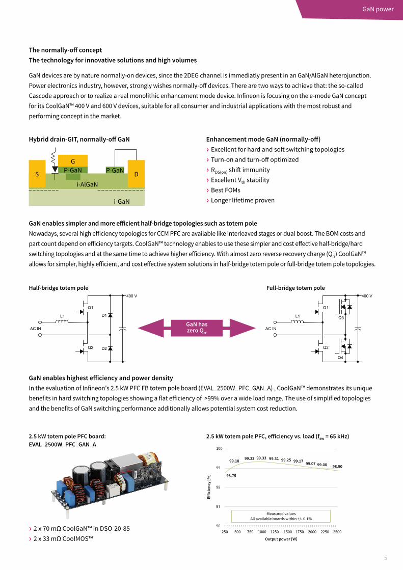
The normally-off concept The technology for innovative solutions and high volumes
GaN devices are by nature normally-on devices, since the 2DEG channel is immediatly present in an GaN/AlGaN heterojunction. Power electronics industry, however, strongly wishes normally-off devices. There are two ways to achieve that: the so-called Cascode approach or to realize a real monolithic enhancement mode device. Infineon is focusing on the e-mode GaN concept for its CoolGaN™ 400 V and 600 V devices, suitable for all consumer and industrial applications with the most robust and performing concept in the market.
Enhancement mode GaN (normally-off) › Excellent for hard and soft switching topologies
› Turn-on and turn-off optimized
› RDS(on) shift immunity
› Excellent Vth stability
› Best FOMs
› Longer lifetime proven
› 2 x 70 mΩ CoolGaN™ in DSO-20-85
› 2 x 33 mΩ CoolMOS™
Hybrid drain-GIT, normally-off GaN
i-GaN
i-AlGaNS
G
DP-GaN P-GaN
GaN enables simpler and more efficient half-bridge topologies such as totem poleNowadays, several high efficiency topologies for CCM PFC are available like interleaved stages or dual boost. The BOM costs and part count depend on efficiency targets. CoolGaN™ technology enables to use these simpler and cost effective half-bridge/hard switching topologies and at the same time to achieve higher efficiency. With almost zero reverse recovery charge (Qrr) CoolGaN™ allows for simpler, highly efficient, and cost effective system solutions in half-bridge totem pole or full-bridge totem pole topologies.
GaN enables highest efficiency and power densityIn the evaluation of Infineon's 2.5 kW PFC FB totem pole board (EVAL_2500W_PFC_GAN_A) , CoolGaN™ demonstrates its unique benefits in hard switching topologies showing a flat efficiency of >99% over a wide load range. The use of simplified topologies and the benefits of GaN switching performance additionally allows potential system cost reduction.
Full-bridge totem poleHalf-bridge totem pole
AC IN
L1
Q1
Q3
Q2
Q4
400 V
AC IN
L1
Q1
Q2 D2
400 V
D1
GaN haszero Qrr
250 500 750 1000 1250 1500 1750 2000 2250 2500
99.18 99.33 99.33 99.31 99.25 99.17 99.07 99.00 98.90
98.75
Output power [W]
Eic
ienc
y [%
]
100
99
98
97
96
Measured valuesAll available boards within +/- 0.1%
2.5 kW totem pole PFC, efficiency vs. load (fsw = 65 kHz)2.5 kW totem pole PFC board:EVAL_2500W_PFC_GAN_A
www.infineon.com/gan
6
GaN power
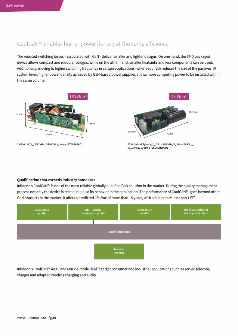
CoolGaN™ enables higher power density at the same efficiency
The reduced switching losses - associated with GaN - deliver smaller and lighter designs. On one hand, the SMD packaged device allows compact and modular designs, while on the other hand, smaller heatsinks and less components can be used. Additionally, moving to higher switching frequency in certain applications (when required) reduces the size of the passives. At system level, higher power density achieved by GaN-based power supplies allows more computing power to be installed within the same volume.
65 W hybrid flyback, fsw 72 to 196 kHz, Vin 90 to 264 Vrms, Vout 3 to 20 V, using IGLD60R190D1
16.5 mm91 mm
152 mm
32 mm
36.5 mm
160 W/in3
75 mm
24 W/in3
3.6 kW LLC, fsw 350 kHz , 380 V-54 V, using IGT60R070D1
Applicationprofile
Degradationmodels
Qualification plan
Rel. investigation atdevelopment phase
QRP – qualityrequirement profile
Released product
Qualification that exceeds industry standardsInfineon’s CoolGaN™ is one of the most reliable globally qualified GaN solution in the market. During the quality management process not only the device is tested, but also its behavior in the application. The performance of CoolGaN™ goes beyond other GaN products in the market. It offers a predicted lifetime of more than 15 years, with a failure rate less than 1 FIT.
Infineon's CoolGaN™ 400 V and 600 V e-mode HEMTs target consumer and industrial applications such as server, telecom, charger and adapter, wireless charging and audio.

www.infineon.com/gan-eicedriver
7
GaN driver
Infineon's CoolGaN™ 400 V and 600 V e-mode HEMTs enable 98% + system efficiency and help customers to make their end products smaller and lighter. Driving enhancement mode devices requires some additional features when choosing the correct gate driver IC; however, CoolGaN™ technology does not require customized ICs. Infineon introduces three new members of its single-channel galvanically isolated gate driver IC family. The new components are a perfect fit for enhancement mode GaN HEMTs with non-isolated gate (diode input characteristic) and low threshold voltage, such as CoolGaN™.
GaN EiceDRIVER™ family Single-channel isolated gate-driver ICs for enhancement mode GaN HEMTs
Complete support for all requirements specific to e-mode GaN HEMTs operation: › Low driving impedance (on-resistance 0.85 Ω source, 0.35 Ω sink)
› Resistor programmable gate current for steady on-state (typical 10 mA)
› Programmable negative gate voltage to completely avoid spurious turn-on in half-bridges
CoolMOS™
CoolMOS™
OptiMOS™
OptiMOS™
OptiMOS™
OptiMOS™
ACLINE
EMIfilter
PFCcontroller
GaN EiceDRIVER™1EDF5673*
EiceDRIVER™2EDF7275
LLCcontroller
GaN EiceDRIVER™1EDS5663H*
Totem poleFull-bridge PFC Resonant LLC Synchronous
rectifier
High voltageCoolGaN™
High voltageCoolGaN™
High voltageCoolGaN™
High voltageCoolGaN™
High voltageCoolGaN™
High voltageCoolGaN™
*GaN EiceDRIVER™ ICs are single-channel products
EiceDRIVER™2EDF7275
Block diagram: typical application example – totem pole full-bridge PFC

8
CoolGaN™ in server Enabling the efficient data flow and storage
Internet of Things (IoT), big data, machine learning and artificial intelligence are driving the power demand for servers and data centers, posing new challenges to SMPS efficiency and form factors. Data center architects face the challenge to increase the delivered power in a given form factor and/or increase efficiency levels to reduce operating costs of server farms.
Both challenges can be addressed with Infineon’s CoolGaN™ technology. By implementing CoolGaN™ in a totem pole PFC combined with a LLC DC-DC stage, more than 98.5% system efficiency can be achieved (for 48 V output voltage systems) providing a total of 2 billion kWh annual savings for US data centers (~ 300 million USD annual savings at 0.15 USD / kWh). Additionally, GaN based SMPS solutions will enable doubling of computed power per rack by pushing the power density to >80 W/in3 from today’s typical ~30 – 40 W/in3 silicon-based solutions.
The outstanding performance of Infineon CoolGaN™ is demonstrated in a full-bridge totem pole PFC board (EVAL_2500W_PFC_GAN_A), reaching >99% peak efficiency. The system has been designed using CoolGaN™ 600 V, 70 mΩ devices in a PG-DSO-20 bottom-side cooled package (IGO60R070D1).
DC
Auxiliary power
Control and housekeeping
AC
Vin Vout
DC
Vaux
PFC-PWM with AUX and ICs
RectificationPFC Main stage
Vbus
CoolGaN™ in server

9
CoolGaN™ in server
Functional block Product category Topology Product family Benefits
PFC High voltage MOSFETs CCM/interleaved PFC; TTF 600 V/650 V CoolMOS™ C7600 V/650 V CoolMOS™ C7 Gold in TOLL
› Best FOM RDS(on)*QG and RDS(on)*Eoss › Lowest RDS(on) per package › Low dependency of switching losses form Rg,ext
High voltage GaN Totem pole PFC CoolGaN™ 600 V › Enable the highest efficiency and highest power density
SiC diodes CCM/interleaved PFC 650 V CoolSiC™ Schottky diode generation 5
› Low FOM VF*QG
Control ICs CCM PFC IC ICE3PCS0xG › Ease-of-use
GaN driver IC Totem pole PFC EiceDRIVER™ 1EDF5673F and 1EDF5673K
› Low driving impedance (on-resistance 0.85 Ω source, 0.35 Ω sink) › Input-output propagation delay accuracy: ±5 ns › Functional and reinforced isolation available
Main stage High voltage MOSFETs ITTF 600 V CoolMOS™ C7/P6 › Fast switching speed for improved efficiency and thermals, low gate charge for enhanced light load efficiency and low power consumption at no load condition › Optimized VGS threshold for lower turn-off losses › Rugged body diode which prevents device failure during hard commutation
LLC, half-bridge below 1 kW
600 V CoolMOS™ P7/CFD6 › Low turn-off losses › Low Qoss › Low QG
LLC, phase shift full-bridge below 1 kW
600 V CoolMOS™ CFD7650 V CoolMOS™ CFD2
› Fast and rugged body diode › Optimized low QG and soft commutation behavior to reach highest efficiency › Highest reliability for 650 V VDS
ZVS PS FB; LLC, TTF 650 V TRENCHSTOP™ F5 › Improved ruggedness and high efficiency in low inductance designs
Control ICs HB LLC IC ICE1HS01G-1 › High efficiency and low EMI
ICE2HS01G
GaN driver IC LLC, ZVS phase shift full-bridge
EiceDRIVER™ 1EDS5663H
› Low driving impedance (on-resistance 0.85 Ω source, 0.35 Ω sink) › Input-output propagation delay accuracy: ±5 ns › Functional and reinforced isolation available
GaN e-mode HEMTs LLC, ZVS phase shift full-bridge
CoolGaN™ 600 V › Enable the highest efficiency and highest power density
Sychronous rectification Low voltage MOSFETs HB LLC and centertap 40 V OptiMOS™ › High efficiency over whole load range, layout tolerance
ITTF 60 V OptiMOS™ › High efficiency, low thermals, low VDS overshoot
ZVS PS FB and center-tap 80 V OptiMOS™ › High efficiency over whole load range, low VDS overshoot and oscillations
Auxiliary power supply Control ICs QR/FF flyback CoolSET™ ICE2QRxx80(Z)(G) 800 V ICE3xRxx80J(Z)(G) 800 V ICE5QRxx70A(Z)(G) 700 V ICE5QRxx80A(Z)(G) 800 V
› Low standby power, high efficiency and robustness › An integrated 700 V/800 V superjunction power MOSFET with avalanche capability › Burst mode entry/exit to optimize standby power at different low load conditions
Housekeeping Microcontrollers - XMC1xxx › Flexibility, HR PWM, digital communication › ARM® based standard MCU family and wide family
Conversion Microcontrollers - XMC4xxx › Flexibility, HR PWM and digital communication
PFC, PWM/resonant converter, synchronous rectification
Gate driver ICs Single-channel isolated EiceDRIVER™ 1EDI Compact
› 100 ns typical propagation delay time › Functional isolation › Separate source
Dual-channel non- isolated
EiceDRIVER™ 2EDNx › 8 V UVLO option › -10 V input robusteness › Output robust against reverse current
Dual-channel isolated EiceDRIVER™ 2EDFx › 35 ns typical propagation delay time › Functional isolation › 1.5 kV CMTI > 150 V/ns
www.infineon.com/server
Product portfolio

10
CoolGaN™ in telecom
CoolGaN™ in telecomFull system solution for telecom power supply
Saving operating and capital expenses, overall power supply footprint and highest solution robustness have been and will remain the major concerns in telecommunication infrastructure development. Infineon’s CoolGaN™ solutions address these challenges by providing benchmark efficiency in the entire operation range, maximizing power density and following Infineon’s stringent qualification regimen.
A 3.6 kW system has been designed using CoolGaN™ 600 V, 70 mΩ (IGT60R070D1) devices in parallel configuration. The system is based on LLC DC-DC topology with up to 400 VDC input and 52.5 V output voltage, delivering up to 3.6 kW of power at 160 W/inch3 power density. Peak efficiency of this system reaches 98.5% (VIN = 390 VDC, Vout = 52.5 V), and remains greater than 97% for loads higher than 20%.
Combining CoolGaN™ in the DC-DC stage with CoolGaN™ based PFC stages will maximize achievable power density and power conversion efficiency, and therefore reduce operating expenses for telecom suppliers. In addition, Infineon’s CoolGaN™ devices and technology have been fully qualified based on industrial requirements to ensure ultimate robustness when deployed in telecom SMPS.
AUX
niPOL, buck
Load
Load
Analog and digital control ICs
DCPFC Main stage
Powerdistribution Hot swap
Primary sidePWM
Synchronousrectification Or-ing
RectificationOr-ing,
hot swap
Battery protection
AC
DC
Vin VBULK Vout
AC-DC rectifier
Isolated DC-DC Non-isolated POL
AUX
Analog and digital control ICs
AC
Vin
DC
Vout
DC
Vaux
AC-DC rectifier
Synchronous
rectificationPFC
DC-DC
main stage
Vbulk
Or-ing
Functional block Product category Topology Product family Benefits
PFC High voltage MOSFETs
CCM/interleaved PFC; TTF
600 V/650 V CoolMOS™ C7
› Best FOM RDS(on)*QG and RDS(on)*Eoss › Lowest RDS(on) per package › Low dependency of switching losses form Rg,ext
600 V CoolMOS™ P7 › Low turn-off losses › Low Qoss › Low QG
High voltage GaN
CCM totem pole CoolGaN™ 600 V › Switching at high frequencies (> Si) › Enables high power density
SiC diodes CCM/interleaved PFC 650 V CoolSiC™ Schottky diode generation 6
› Low FOM VF*QC
Control ICs CCM PFC IC 800 V – ICE3PCS0xG › High PFC and low THD
GaN driver IC Totem-pole PFC EiceDRIVER™ 1EDF5673F and 1EDF5673K
› Low driving impedance (on-resistance 0.85 Ω source, 0.35 Ω sink) › Input-output propagation delay accuracy: ±5 ns › Functional and reinforced isolation available
Product portfolio
www.infineon.com/telecom

11
CoolGaN™ in telecom
Functional block Product category Topology Product family Benefits
DC-DC main stage
High voltage MOSFETs
CCM/interleaved PFC; TTF HB LLC
600 V CoolMOS™ C7/P7 › Fast switching speed for improved efficiency and thermals › Low gate charge for enhanced light load efficiency and low power consumption at no load condition › Optimized VGS threshold for lower turn-off losses › Rugged body diode which prevents device failure during hard commutation
LLC 600 V CoolMOS™ C7 › Low turn-off losses › Low Qoss › Low QG
CCM/interleaved PFC; TTF HB LLC
600 V CoolMOS™ CFD7 › Best-in-class Qrr and trr level › Significant reduced QG › Improved efficiency over previous CoolMOS™ fast body diode series
Control ICs HB LLC IC ICE1HS01G-1, ICE2HS01G › High efficiency and low EMI
GaN driver IC LLC, ZVS phase shift full-bridge
EiceDRIVER™ 1EDS5663H › Low driving impedance (on-resistance 0.85 Ω source, 0.35 Ω sink) › Input-output propagation delay accuracy: +/- 5 ns › Functional and reinforced isolation available
GaN e-mode HEMTs
LLC, ZVS phase shift full-bridge
CoolGaN™ 600 V › Enable the highest efficiency and highest power density
Synchronous rectification
Low voltage MOSFETs
Synchronous rectification MOSFET
OptiMOS™ 80-150 V › Industry’s lowest FOM (RDS(on)*QG) leading to high efficiency at good price/performance › Low voltage overshoots enabling easy design-in › Industry’s lowest RDS(on) › Highest system efficiency and power density › Outstanding quality and reliability › Reduces the need for a snubber circuit
Auxiliary power supply
Control ICs 5th generation QR/FF flyback CoolSET™
QR 800 V - ICE5QRxx80AxFF 800 V - ICE5xRxx80AG
› Quasi-resonant switching operation for high efficiency and low EMI signature › Fixed frequency switching operation for ease-of-design – 100 KHz and 125 KHz › Fast and robust start-up with cascode configuration › Robust protection with adjustable line input over-voltage protection, VCC and CS pin short-to-ground protection › Optimized light-load efficiency with selectable burst mode entry/exit profile › Frequency reduction for mid and light load condition to reduce switching losses and increase efficiency › Direct feedback and regulation with integrated error amplifier for non-isolated output › High power delivery of up to 42 W with 800 V heatsink-less SMD package CoolSET™
Housekeeping Microcontrollers - XMC1xxx › Flexibility, HR PWM, digital communication › ARM® based standard MCU family and wide family
Conversion Microcontrollers - XMC4xxx › Flexibility, HR PWM, digital communication › ARM® based standard MCU family and wide family
PFC, PWM/ resonant converter, synchronous rectification
Gate driver ICs Single channel non-isolated
EiceDRIVER™ 1EDN751x › 8 V UVLO option › (-)10 V input robustness › Output robust against reverse current
Single channel non-isolated
EiceDRIVER™ 1EDN7550 › 8 V UVLO option › (-)10 V input robustness › True differential inputs for >100 VAC ground shift robustness
Dual channel non-isolated
EiceDRIVER™ 2EDN7x › 8 V UVLO option › (-)10 V input robustness › Output robust against reverse current
Dual channel junction isolated
EiceDRIVER™ 2EDL811x* › 20 ns typ. propagation delay time › 20 V bootstrap capability on high side › (-)7 V input robustness
Single channel isolated
EiceDRIVER™ 1EDi Compact › 100 ns typ. propagation delay time › Functional isolation 1.2 kV separate source and sync outputs
Dual channel isolated EiceDRIVER™ 2EDFx › 35 ns typ. propagation delay time › Functional isolation 1.5 kVCMTI > 150 V/ns
Dual channel isolated EiceDRIVER™ 2EDSx › 35 ns typ. propagation delay time › Reinforced (safe) isolation 6 kV CMTI > 150 V/ns
Or-ing Low voltage MOSFETs
Or-ing MOSFET OptiMOS™ 60-200 V › Industry’s lowest FOM (RDS(on)*QG) leading to high efficiency at good price/performance › Low voltage overshoots enabling easy design-in
Battery protection
Low voltage MOSFETs
MOSFET OptiMOS™ 60-150 V
Isolated DC-DC Low voltage MOSFETs
Primary side PWM MOSFET
OptiMOS™ 60-200 V › Industry’s lowest RDS(on) › Highest system efficiency and power density › Outstanding quality and reliability › Reduces the need for a snubber circuit
StrongIRFET™ 60-200 V
Small Signal 60-200 V
Synchronous rectification MOSFET
OptiMOS™ 40-100 V
StrongIRFET™ 40-100 V
Or-ing MOSFET OptiMOS™ 25-30 V
StrongIRFET™ 25-30 V* Upcoming Q1 2019

12
CoolGaN™ in wireless charging
CoolGaN™ in wireless chargingEnabling the next level of charging
The prospect of wirelessly charging our mobile devices has been around for years and has recently become reality with the proliferation of inductive wireless charging technology. However, to make wireless charging truly ubiquitous and offer improved end-user convenience (e.g., improved freedom of positioning), wireless charging solutions need to further evolve, and likely will apply the magnetic-resonance technology over time. For the latter, high transmission frequencies (multiple MHz) are required, which poses significant challenges to standard silicon power technologies within the transmitter and the receiver devices. Infineon is developing resonant solutions for transmitter, receiver and adapter to serve the upcoming requirements of various wireless charging applications.
Due to its significantly reduced parasitic capacitances, CoolGaN™ technology is the ideal choice when switching at frequencies in the MHz range (e.g., 6.78 MHz as required by the resonant AirFuel wireless charging standard).
Class E and class D topologies are the main topologies of choice when resonant wireless charging is applied. Both topologies reduce switching losses by transitioning between on- and off-switching position of the power devices at zero volt across the respective power switch. In the class D ZVS topology, lower breakdown voltage devices can be used, thereby increasing the overall system efficiency. In the class E topology, however, simpler driver architecture (low-side only) and only a single switch per class Ebranch offer the prospects of reduced system cost. CoolGaN™ is ideally suited to address both topologies by either maximizing overall system performance (in class D implementations) or reducing overall system solution cost (in class E implementation).
Infineon’s CoolGaN™ devices have been successfully tested in a 16 W class E wireless charging demonstrator system as well as in customer implementations operating at 6.78 MHz at higher watt class.
Having a reliable partner by your side is key to maximize the performance and consumer appeal of your wireless charging designs. At Infineon, we help you master your design challenges with our broad selection of semiconductors and our powerful CoolGaN™ products.
System diagram: resonant class E single-ended with CoolGaN™
Target applications
CoolGaN™e-mode HEMTs
XMC™ or wirelesspower controller
ReceiverGate Driver
AC-DC converter Pre regulators
EiceDRIVER™gate driver IC

13
CoolGaN™ in wireless charging
Sub-application Voltage class Package Part number RDS(on) max @ VGS = 4.5 V [mQ]
QG typical[nC]
Coss typical[pF] Topology
Inverter MOSFETs 30 V PQFN 2 x 2 Dual IRLHS6376PbF 48 2.8 32 Class DPQFN 3.3 x 3.3 Dual BSZ0909ND 25 1.8 120 Class D
BSZ0910ND 13 5.6 230 Class DSOT 23 IRLML0030pbf 33 2.75 84 Class D
40 V SOT 23 IRLML0040pbf 62 2.8 49 Class D60 V SOT 23 IRLML0060pbf 98 2.6 37 Class D80 V PQFN 2 x 2 IRL80HS120 32 2.5 68 Class D/E100 V PQFN 2 x 2 IRL100HS121 42 2.7 62 Class D/E150 V PQFN 3.3 x 3.3 BSZ900N15NS3 75** 4.1** 46 Class E
BSZ520N15NS3 42** 7.2** 80 Class E200 V BSZ900N20NS3 78** 7.2** 52 Class E
BSZ22DN20NS3 200** 3.5** 24 Class EBSZ12DN20NS3 111** 5.4** 39 Class E
250 V BSZ42DN25NS3 375** 3.6** 21 Class E
Driver ICs EiceDRIVER™ 2EDL71* EiceDRIVER™ 1EDN7512, 2EDN7524EiceDRIVER™ GaN driver IC 1EDS5663H, 1EDF5673F, 1EDF5673K
GaN e-mode HEMTs CoolGaN™ 600 V e-mode GaN HEMT IGT60R190D1S (HDSOF-8-3)
Microcontroller XMC™ MCU and wireless power controller XMC™-SC* (including software IP)
Voltage regulators IR3841MPbF, IFX20002, IFX91041EJV50, IFX90121ELV50, IFX81481ELV
Small signal MOSFETs Please check online
* Coming soon** VGS = 8 V
Components for resonant (AirFuel) and high frequency solutions
Find the right solutions for your wireless charging designs in four steps
For Infineon’s complete offering of devices for inductive, resonant or in-cabin car charging access the Infineon wireless charging selection tool that allows you to find the right solutions for your designs in just four steps: select the application, power range, standard and the topology you want to apply and get an overview of Infineon’s most recommended offerings.
www.infineon.com/wirelesscharging

14
GaN EiceDRIVER™ familySingle-channel isolated gate-driver ICs for enhancement mode GaN HEMTs
Interested? Learn more at: www.infineon.com/gan
Release the full potential of GaN e-mode HEMTs with Infineon’s silicon-based drivers. The combined solution of CoolGaNTM and EiceDRIVERTM reduces the complexity in customer design, bringing ease-of-use into modern topologies.

15
CoolGaN™ in adapter/charger
CoolGaN™ in adapter and chargerBreakthrough in power density
Travelling with multiple and often clunky chargers and adapters for phones, tablets and laptops has been a nuisance for many consumers, and often leads to frustrations due to the additional weight and required space. Over the past years, manufacturers of chargers and adapters became increasingly aware of these issues and a trend towards higher power density and consequently smaller devices has emerged. Today, the typical power topology used in such systems is a flyback power conversion topology, and the form factor is limited by the efficiency achievable at 90 VAC input voltage and full load. The highest power density systems available today reach ~12 W/in3 (for 65 W maximum output power).
Infineon’s CoolGaN™ supports a breakthrough with respect to power density for adapter and charger systems, enabling ~20 W/in3 power density systems (for 65 W maximum output power). This advantage can be realized by implementing Infineon’s CoolGaN™ in a half-bridge topology that allows increasing switching frequency and efficiency simultaneously.
Functional block Product category Topology Product family Benefits
Flyback converter
High voltage MOSFETs Flyback 600 V/700 V/800 VCoolMOS™ P7
› Fast switching speed for improved efficiency and thermals › Reduced gate charge for enhanced light load efficiency › Optimized VGS threshold for lower turn-off losses
Active clamp flybackHybrid flyback
CoolGaN™ 600 V › Highest efficiency › Highest power density
Low voltage MOSFETs Flyback/auxiliary synchronous rectification
OptiMOS™ 100 V-150 V › Low conduction losses and reduced overshoot › Logic level can support low voltage gate drive to achieve high efficiency
Control ICs QR flyback IC ICE2QS03G, ICE5QSAG › High efficiency and low standby power
FFR flyback IC IDP2105 › High power density and digital control
PFC High voltage MOSFETs DCM PFC 600 V CoolMOS™ P7 › Fast switching speed for improved efficiency › Reduced gate charge for enhanced light load efficiency › Optimized VGS threshold for lower turn-off losses
ZVS totem pole CoolGaN™ 600 V › Highest efficiency contribution via less parasitic parameter › Space saving with SMD smaller package
DCM PFC 650 V Rapid 1 › Easy control of switching behavior due to higher RG,int › Better transition losses versus standard MOSFET
Boost diode DCM/PFC 650 V Rapid 1 › Low conduction losses
Control ICs DCM PFC ICs TDA4863G, IRS2505LTRPBF
› Simple external circuitry › High power factor and low THD
Main stage High voltage MOSFETs HB LLC 600 V CoolMOS™ P7 › Fast switching speed for improved efficiency and thermals › Reduced gate charge for enhanced light load efficiency › Optimized VGS threshold for lower turn-off losses
CoolGaN™ 600 V › Highest efficiency › Highest power density
Synchronous rectification
Low voltage MOSFETs Synchronous rectification OptiMOS™ 5 100 V-150 V › Low conduction losses, reduced overshoot › Logic level switching
Control ICs Synchronous rectification IR1161LTRPBF › High efficiency › Simple external circuitry
www.infineon.com/smps

16
CoolGaN™ for class D audioMaximize audio performance
Class D audio amplifiers have practically eliminated class A/B amplifiers as they offer greatly improved energy efficiency, and thereby enable small form factor designs for even high power amplification. In addition, class D audio amplifiers theoretically can reach 0% distortion and 100% energy efficiency in case the power switch in the class D stage is an ideal switch that results in excellent sound quality and practically negligible thermal design limitations.
CoolGaN™ 400 V is tailored for premium HiFi home audio, professional, and aftermarket car audio systems where end users demand every detail of their high-resolution soundtracks. These have been conventionally addressed by bulky linear or tube amplifiers. With CoolGaN™ 400 V as class D output stage, audio designers are able to deliver the best listening experience to their prospective audio fans.
Infineon’s CoolGaN™ technology allows approaching the theoretical ideal performance of class D audio amplifiers due to its unique characteristics, perfectly suited for this application: zero reverse recovery charge (Qrr) of the body diode, linear input and output capacitances, and extremely fast switching speeds (lowest QGD and Rg) result in ideal switching waveforms, close to an ideal switch. These ideal switching waveforms are the prerequisite to maximize audio performance and minimize power losses in class D audio amplifiers.
CoolGaN™ in audio
Infineon’s audio solutions
www.infineon.com/audiosolutions
Output power [W/Channel]
Scalable in output power Best audio performanceHighest power w/o heatsinkLowest idle power
No heatsink
20
Digi
tal i
nput
Anal
og in
put
100 1000 2000
w/gate buffer
IRS209X (1 ch) + CoolGaN™ 400 V e-mode HEMTs
IRS2092SPBF (1 ch) + MOSFETs
IRS2052M (2 ch) + MOSFETs
IRS2093MPBF (4 ch) + MOSFETs
IR43x1 (1 ch)
IR43x2 (2 ch)
MA12040 (1 – 4 ch)
MA12070 (1 – 4 ch)
MA12040P (1 – 4 ch)
MA12070P (1 – 4 ch)
Inte
grat
ed IC
sIC
s + M
OSF
ETs/
e-m
ode
GaN

17
CoolGaN™ in audio
Class D driver IC selection guide
CoolGaN™ 400 V e-mode GaN HEMTs for class D audio product offering
IRS20965S IRS20957SPBF IRS2092SPBF IRS2052M IRS2093MPBF IRS2452AM
Specifications Number of audio channels 1 1 1 2 4 2
Max. power per channel 500 W 500 W 500 W 300 W 300 W 500 W
Supply voltage ±100 V ±100 V ±100 V ±100 V ±100 V ±200 V
Gate sink/source current 2.0/2.0 A 1.2/1.0 A 1.2/1.0 A 0.6/0.5 A 0.6/0.5 A 0.6/0.5 A
Features Over-current protection
Over-current flag
PWM input
Floating input
Dead time
Protection control logic
PWM controller
Clip detection
Click noise reduction
Temperature sensor input
Thermal shutdown
Clock input
Package type 16pin SOIC narrow
16pin SOIC narrow
16pin SOIC narrow
MLPQ48 MLPQ48 MLPQ32
Reference design - IRAUDAMP4A IRAUDAMP6
IRAUDAMP5 IRAUDAMP7S IRAUDAMP7D IRAUDAMP9
IRAUDAMP10 IRAUDAMP8 EVAL_IRAUDAMP23
PG-HSOF-8-3 (TO-leadless)
Pmax Up to 200 W
RDS(on) max. 70 Ω
Typical part number IGT40R070D1 E8220
Integrated class D audio modules
IR4301M IR4321M IR4311M IR4302M IR4322M IR4312M
Specifications Number of audio channels 1 1 1 2 2 2
Max. power per channel 160 W 90 W 45 W 130 W 100 W 40 W
Supply voltage ~ ±34 V or 68 V ~ ±25 V or 50 V ~ ±15 V or 32 V ~ ±32 V or 64 V ~ ±25 V or 50 V ~ ±16 V or 32 V
Max. PWM frequency 500 kHz 500 kHz 500 kHz 500 kHz 500 kHz 500 kHz
Features Differential audio input
Over-current protection
Integrated power MOSFET (80 V) (60 V) (40 V) (80 V) (60 V) (40 V)
PWM controller
Thermal shutdown
Click noise reduction
Clip detection
Fault output
Package type 5 x 6 mm QFN 5 x 6 mm QFN 5 x 6 mm QFN 7 x 7 mm QFN 7 x 7 mm QFN 7 x 7 mm QFN
Reference design IRAUDAMP12 IRAUDAMP19
IRAUDAMP21 IRAUDAMP15 IRAUDAMP16 IRAUDAMP17
IRAUDAMP22 IRAUDAMP18
Product portfolio
Product name Peak output [W]
Input type Supply voltage [V]
Main features Orderable part number
MA12040P 2x40 I2S digital audio input 4–18 Digital volume control and limiter MA12040PXUMA1
MA12040 2x40 Analog audio input 4–18 Selectable gain (20 dB/26 dB) MA12040XUMA1
MA12070P 2x80 I2S digital audio input 4–26 Digital volume control and limiter MA12070PXUMA1
MA12070 2x80 Analog audio input 4–26 Selectable gain (20 dB/26 dB) MA12070XUMA1

18
Discover 3D models of the boards and get access to GaN training materials:www.infineon.com/gan
CoolGaN™ evaluation environment
CoolGaN™ boardsDriving the innovation
Infineon’s CoolGaN™ devices benefit from Infineon’s innovative spirit towards challenging applications like telecom rectifiers, SMPS servers, or class D audio where CoolGaN™ technology proved to be highly reliable. It is the most rugged and reliable solution in the market, available in high performing SMD packages to fully exploit the benefits of GaN. With a set of available evaluation boards, comprehensive online training materials and a global support structure Infineon allows for an easier transition to these new technologies and allows for faster prototyping and go-to-market.
*Order on request
PFC for server SMPS and telecom rectifiers – 99.3% peak efficiency › 2.5 kW totem pole PFC using IGO60R070D1 (70 mΩ/600 V in DSO-20-85 bottom-side cooling)
› Order code: EVAL_2500W_PFC_GAN_A
LLC for telecom rectifiers – ~160 W/in3 @ >98% peak efficiency › 3.6 kW LLC, 52 V Vout, 350 kHz using IGT60R070D1 in primary side (70 mΩ/600 V in TO-leadless)
› Order code: EVAL_3K6W_LLC_GAN*
High frequency (>1 MHz) half-bridge platform › Functional board with 2 x 1EDF5673K in LGA package, 2 x IGOT60R070D1 (DSO-20-87 top-side cooling packages)
› Order code: EVAL_1EDF_G1_HB_GAN
200 W + 200 W class D audio amplifier › 200 W + 200 W class D audio amplifier boards, ±75 Vin using IGT40R070D1 E8220 (70 mΩ in TO-leadless package)
› Order code: EVAL_AUDAMP24*
19
www.infineon.com/ganwww.infineon.com/gan-eicedriver
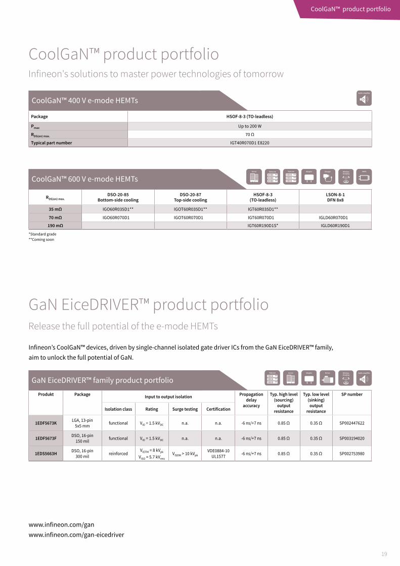
CoolGaN™ product portfolio
CoolGaN™ product portfolioInfineon's solutions to master power technologies of tomorrow
GaN EiceDRIVER™ product portfolioRelease the full potential of the e-mode HEMTs
Infineon’s CoolGaN™ devices, driven by single-channel isolated gate driver ICs from the GaN EiceDRIVER™ family, aim to unlock the full potential of GaN.
RDS(on) max.DSO-20-85
Bottom-side coolingDSO-20-87
Top-side coolingHSOF-8-3
(TO-leadless)LSON-8-1DFN 8x8
35 mΩ IGO60R035D1** IGOT60R035D1** IGT60R035D1**
70 mΩ IGO60R070D1** IGOT60R070D1** IGT60R070D1** IGLD60R070D1**
190 mΩ IGT60R190D1S* IGLD60R190D1
*Standard grade**Coming soon
CoolGaN™ 400 V e-mode HEMTs
Package HSOF-8-3 (TO-leadless)
Pmax Up to 200 W
RDS(on) max. 70 Ω
Typical part number IGT40R070D1 E8220
CoolGaN™ 600 V e-mode HEMTs ChargerCharger
GaN EiceDRIVER™ family product portfolio
Produkt Package Input to output isolation Propagationdelay
accuracy
Typ. high level (sourcing)
output resistance
Typ. low level (sinking)
output resistance
SP number
Isolation class Rating Surge testing Certification
1EDF5673K LGA, 13-pin 5x5 mm functional VIO = 1.5 kVDC n.a. n.a. -6 ns/+7 ns 0.85 Ω 0.35 Ω SP002447622
1EDF5673F DSO, 16-pin 150 mil functional VIO = 1.5 kVDC n.a. n.a. -6 ns/+7 ns 0.85 Ω 0.35 Ω SP003194020
1EDS5663H DSO, 16-pin 300 mil reinforced
VIOTM = 8 kVpk
VISO = 5.7 kVrmsVISOM > 10 kVpk
VDE0884-10UL1577 -6 ns/+7 ns 0.85 Ω 0.35 Ω SP002753980

20
CoolGaN™ nomenclature
CoolGaN™ nomenclature
I G T 60 R 070 D 1
Package type
LD = DFN 8 x 8-LSON
T = TOLL
O = DSO20-BSC
OT = DSO20-TSC
Generation
1 = 1st generation
Product type
D = Discrete
S = System
Company
I = Infineon
Technology
G = GaN
Voltage
Divided by 10 (60x10 = 600 V)
RDS(on) [mΩ]
R = RDS(on)
Reliability grade
blank = Industrial
A = Automotive
S = Standard

Part of your life. Part of tomorrow.
A world leader in semiconductor solutions
Our missionWe make life easier, safer and greener.
Our valuesWe commitWe partnerWe innovateWe perform
Our visionWe are the link between the real and the digital world.

22
Notes

23
Notes

Service hotline
Infineon offers its toll-free 0800/4001 service hotline as one central number, available 24/7 in English, Mandarin and German.
› Germany .................... 0800 951 951 951 (German/English)
› China, mainland ....... 4001 200 951 (Mandarin/English)
› India .......................... 000 800 4402 951 (English)
› USA ............................ 1-866 951 9519 (English/German)
› Other countries ......... 00* 800 951 951 951 (English/German)
› Direct access ............. +49 89 234-0 (interconnection fee, German/English)
* Please note: Some countries may require you to dial a code other than “00” to access this international number. Please visit www.infineon.com/service for your country!
Where to buy
Infineon distribution partners and sales offices: www.infineon.com/WhereToBuy
Published byInfineon Technologies Austria AG9500 Villach, Austria
© 2019 Infineon Technologies AG.All rights reserved.
Order number: B152-I0892-V1-7600-EU-EC-PDate: 09 / 2019
Please note!THIS DOCUMENT IS FOR INFORMATION PURPOSES ONLY AND ANY INFORMATION GIVEN HEREIN SHALL IN NO EVENT BE REGARDED AS A WARRANTY, GUARANTEE OR DESCRIPTION OF ANY FUNCTIONALITY, CONDITIONS AND/OR QUALITY OF OUR PRODUCTS OR ANY SUITABILITY FOR A PARTICULAR PURPOSE. WITH REGARD TO THE TECHNICAL SPECIFICATIONS OF OUR PRODUCTS, WE KINDLY ASK YOU TO REFER TO THE RELEVANT PRODUCT DATA SHEETS PROVIDED BY US. OUR CUSTOMERS AND THEIR TECHNICAL DEPARTMENTS ARE REQUIRED TO EVALUATE THE SUITABILITY OF OUR PRODUCTS FOR THE INTENDED APPLICATION.
WE RESERVE THE RIGHT TO CHANGE THIS DOCUMENT AND/OR THE INFORMATION GIVEN HEREIN AT ANY TIME.
Additional informationFor further information on technologies, our products, the application of our products, delivery terms and conditions and/or prices, please contact your nearest Infineon Technologies office (www.infineon.com).
WarningsDue to technical requirements, our products may contain dangerous substances. For information on the types in question, please contact your nearest Infineon Technologies office.
Except as otherwise explicitly approved by us in a written document signed by authorized representatives of Infineon Technologies, our products may not be used in any life- endangering applications, including but not limited to medical, nuclear, military, life-critical or any other applications where a failure of the product or any consequences of the use thereof can result in personal injury.
Mobile product catalog
Mobile app for iOS and Android.
www.infineon.com