conversion in optical and metasurfaces: and fabrication · 20, , ()() 20. ·) ·)
TRANSCRIPT

Opto-Electronic Advances
Review2018, Vol. 1, No. 10
180021‐1
© 2018 Institute of Optics and Electronics, Chinese Academy of Sciences. All rights reserved.
DOI: 10.29026/oea.2018.180021
Nonlinear frequency conversion in optical nanoantennas and metasurfaces: materials evolution and fabrication MohsenRahmani1*,GiuseppeLeo2,IgalBrener3,AnatolyV.Zayats4, StefanA.Maier5,6,CostantinoDeAngelis7,HoeTan1,ValerioFlavioGili2,FouadKarouta1,RupertOulton5,KaushalVora1,MykhayloLysevych1,IsabelleStaude8,LeiXu9,AndreyE.Miroshnichenko9, ChennupatiJagadish1andDragomirN.Neshev1
Nonlinear frequency conversion is one of the most fundamental processes in nonlinear optics. It has a wide range of applications in our daily lives, including novel light sources, sensing, and information processing. It is usually assumedthat nonlinear frequency conversion requires large crystals that gradually accumulate a strong effect. However, the large size of nonlinear crystals is not compatible with the miniaturisation of modern photonic and optoelectronic systems.Therefore, shrinking the nonlinear structures down to the nanoscale, while keeping favourable conversion efficiencies, is of great importance for future photonics applications. In the last decade, researchers have studied the strategies for en-hancing the nonlinear efficiencies at the nanoscale, e.g. by employing different nonlinear materials, resonant couplings and hybridization techniques. In this paper, we provide a compact review of the nanomaterials-based efforts, ranging from metal to dielectric and semiconductor nanostructures, including their relevant nanofabrication techniques.
Keywords: nonlinear nanophotonics; metallic nanoantennas; dielectric nanoantennas; III-V semiconductor nanoantenna;nanofabrication
Rahmani M, Leo G, Brener I, Zayats A V, Maier S A, et al. Nonlinear frequency conversion in optical nanoantennas and metasurfaces:
materials evolution and fabrication. Opto‐Electronic Advances 1, 180021 (2018).
Introduction Advanced nanofabrication techniques have enabled com-plicated assemblies of nanoscale structures that can be employed for engineering the electromagnetic behaviour at optical frequencies. Nanophotonics, i.e. the technology of generating, controlling, and detecting photons, via
engineered nanostructures, is considered to be a revolu-tionary technology for the 21st Century1. The field of intense light interaction with nanostructures, so called nonlinear nanophotonics, is one of the most attractive branches of nanophotonics that studies multifrequencies interactions in nanoscale devices, including the distribu-tion and guiding the generated frequencies in selected
1Research School of Physics and Engineering, The Australian National University, Canberra ACT 2601, Australia; 2Matériaux et Phénomènes
Quantiques, Université Paris Diderot-Sorbonne Paris Cité, 10 rue A. Domon et L. Duquet, 75013 Paris, France; 3Center for Integrated
Nanotechnologies, Sandia National Laboratories, Albuquerque, New Mexico 87185, United States; 4Department of Physics, King’s College Lon-
don, Strand, London WC2R 2LS, United Kingdom; 5The Blackett Laboratory, Department of Physics, Imperial College London, London, SW7
2AZ, United Kingdom; 6Chair in Hybrid Nanosystems, Nano Institute Munich, Fakultät für Physik, Ludwig-Maximilians-Universität München,
München, Germany; 7Deptartment of Information Engineering, Universitàdegli Studi di Brescia and INO-CNR, Via Branze 38, 25123 Brescia,
Italy; 8Institute of Applied Physics, Abbe Center of Photonics, Friedrich Schiller University Jena, 07745 Jena, Germany; 9School of Engineering
and Information Technology, University of New South Wales, Canberra ACT 2600, Australia
* Correspondence: M Rahmani, E-mail: [email protected]
Received 21 October 2018; accepted 13 November 2018; accepted article preview online 7 December 2018
Opto-Electronic Advances DOI: 10.29026/oea.2018.180021
180021‐2
© 2018 Institute of Optics and Electronics, Chinese Academy of Sciences. All rights reserved.
frequency ranges. This field plays an important role in modern photonic devices, including optical signal pro-cessing, control over the frequency spectrum of laser light, ultrafast switching and generation of ultrashort pulses2,3.
The nonlinear optical response of nanostructured ma-terials is generally very weak. However, recent studies have revealed the potential of nanophotonics to address this issue via artificially induced nonlinear responses in optically resonant nanostructures3–15. This is possible, since metallic and dielectric nanostructures are capable of squeezing light fields into volumes much smaller than the diffraction limit. In other words, nanostructures can act as optical antennas thus reversibly transferring propagat-ing electromagnetic waves into volumes orders of magni-tude smaller than the diffraction limit of light16–18. Such concentration of the optical fields to nanoscale volumes strongly promotes and enhances nonlinear effects at the nanoscale. In particular, nonlinear frequency conversion at the nanoscale can result in novel nanoscale light sources, including sources of single quanta of light. Such sources will advance the performance, energy efficiency and security of future optical communication networks and computing systems. However, the fabrication of non-linear nanoantennas and their functionalities requires novel approaches and materials to efficiently convert op-tical fields from one frequency to another. Importantly, the chosen materials should be resistant enough against heat generated by high-power lasers, and preferably ex-hibit minimal optical losses.
Here, we review the materials evolution and various approaches for fabricating nanostructured materials for nonlinear frequency conversion. We provide detailed analysis of both advantages and disadvantages of each material, in terms of nonlinear properties, nanofabrica-tion and explain why research interests have migrated from one material to another. Notably, the comparison between nonlinear efficiencies and characteristics of nanoantennas, that are already well-reviewed19–22, are beyond the scope of this review paper. This exception
includes the factors that can enhance the conversion effi-ciency but are not necessarily related to the material of antennas, such as mode compositions in the fundamental and/or harmonic generation wavelengths, various types of couplings and various types of mode interferences, etc19–22.
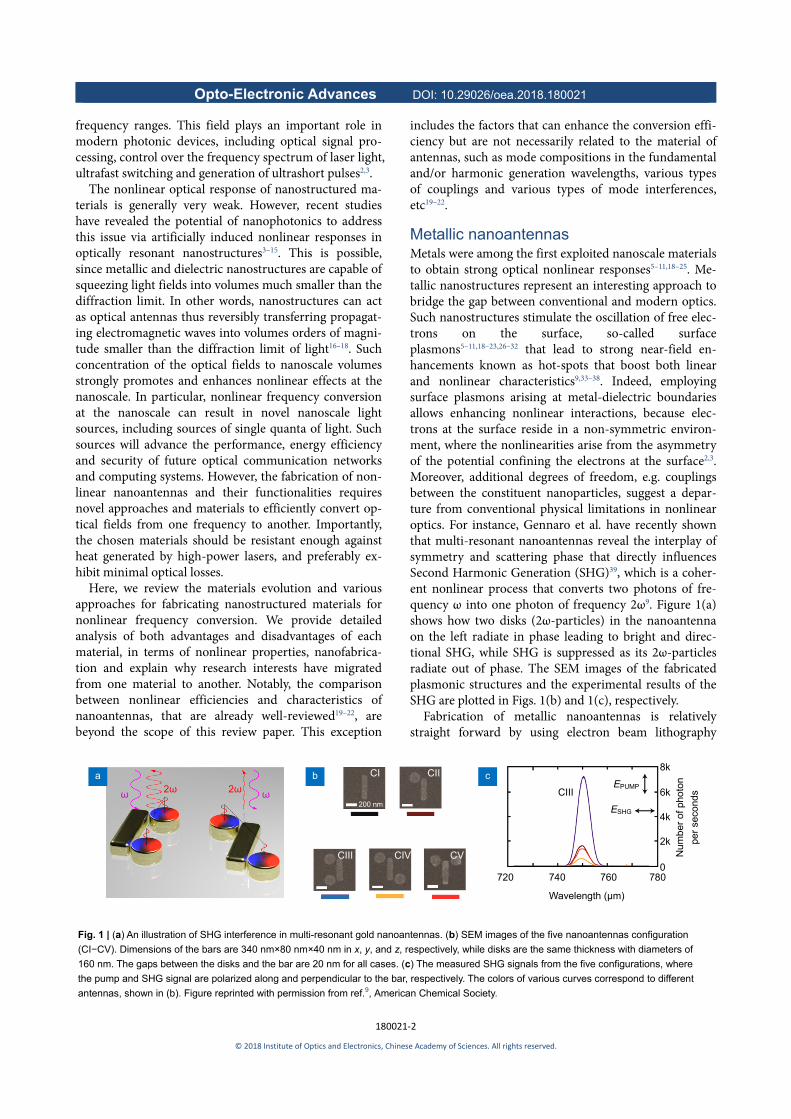
Metallic nanoantennas Metals were among the first exploited nanoscale materials to obtain strong optical nonlinear responses5–11,18–25. Me-tallic nanostructures represent an interesting approach to bridge the gap between conventional and modern optics. Such nanostructures stimulate the oscillation of free elec-trons on the surface, so-called surface plasmons5–11,18–23,26–32 that lead to strong near-field en-hancements known as hot-spots that boost both linear and nonlinear characteristics9,33–38. Indeed, employing surface plasmons arising at metal-dielectric boundaries allows enhancing nonlinear interactions, because elec-trons at the surface reside in a non-symmetric environ-ment, where the nonlinearities arise from the asymmetry of the potential confining the electrons at the surface2,3. Moreover, additional degrees of freedom, e.g. couplings between the constituent nanoparticles, suggest a depar-ture from conventional physical limitations in nonlinear optics. For instance, Gennaro et al. have recently shown that multi-resonant nanoantennas reveal the interplay of symmetry and scattering phase that directly influences Second Harmonic Generation (SHG)39, which is a coher-ent nonlinear process that converts two photons of fre-quency ω into one photon of frequency 2ω9. Figure 1(a) shows how two disks (2ω-particles) in the nanoantenna on the left radiate in phase leading to bright and direc-tional SHG, while SHG is suppressed as its 2ω-particles radiate out of phase. The SEM images of the fabricated plasmonic structures and the experimental results of the SHG are plotted in Figs. 1(b) and 1(c), respectively.
Fabrication of metallic nanoantennas is relatively straight forward by using electron beam lithography
Fig. 1 | (a) An illustration of SHG interference in multi-resonant gold nanoantennas. (b) SEM images of the five nanoantennas configuration
(CI−CV). Dimensions of the bars are 340 nm×80 nm×40 nm in x, y, and z, respectively, while disks are the same thickness with diameters of
160 nm. The gaps between the disks and the bar are 20 nm for all cases. (c) The measured SHG signals from the five configurations, where
the pump and SHG signal are polarized along and perpendicular to the bar, respectively. The colors of various curves correspond to different
antennas, shown in (b). Figure reprinted with permission from ref.9, American Chemical Society.
a b c
ω ω 2ω 2ω
200 nm
CI CII
CIII CIV CV
CIII
720 740 760 780
8k
6k
4k
2k
0
Nu
mb
er o
f pho
ton
per
seco
nds
Wavelength (μm)
EPUMP
ESHG
Opto-Electronic Advances DOI: 10.29026/oea.2018.180021
180021‐3
© 2018 Institute of Optics and Electronics, Chinese Academy of Sciences. All rights reserved.
(EBL). Since metal films can be deposited by electron beam/thermal evaporation or sputtering, both at room temperature, the thin metal film deposition process does not damage the electron beam resist. Therefore, high quality nanoantennas, patterned by an electron beam on the resist, can be transferred to the metal films by a lift-off technique, leading with minimal variations.
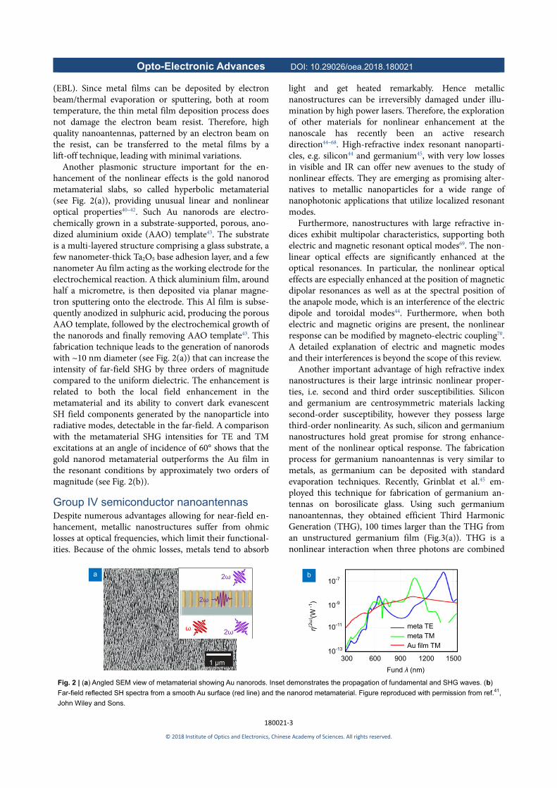
Another plasmonic structure important for the en-hancement of the nonlinear effects is the gold nanorod metamaterial slabs, so called hyperbolic metamaterial (see Fig. 2(a)), providing unusual linear and nonlinear optical properties40–42. Such Au nanorods are electro-chemically grown in a substrate-supported, porous, ano-dized aluminium oxide (AAO) template43. The substrate is a multi-layered structure comprising a glass substrate, a few nanometer-thick Ta2O5 base adhesion layer, and a few nanometer Au film acting as the working electrode for the electrochemical reaction. A thick aluminium film, around half a micrometre, is then deposited via planar magne-tron sputtering onto the electrode. This Al film is subse-quently anodized in sulphuric acid, producing the porous AAO template, followed by the electrochemical growth of the nanorods and finally removing AAO template43. This fabrication technique leads to the generation of nanorods with ~10 nm diameter (see Fig. 2(a)) that can increase the intensity of far-field SHG by three orders of magnitude compared to the uniform dielectric. The enhancement is related to both the local field enhancement in the metamaterial and its ability to convert dark evanescent SH field components generated by the nanoparticle into radiative modes, detectable in the far-field. A comparison with the metamaterial SHG intensities for TE and TM excitations at an angle of incidence of 60° shows that the gold nanorod metamaterial outperforms the Au film in the resonant conditions by approximately two orders of magnitude (see Fig. 2(b)).
Group IV semiconductor nanoantennas Despite numerous advantages allowing for near-field en-hancement, metallic nanostructures suffer from ohmic losses at optical frequencies, which limit their functional-ities. Because of the ohmic losses, metals tend to absorb
light and get heated remarkably. Hence metallic nanostructures can be irreversibly damaged under illu-mination by high power lasers. Therefore, the exploration of other materials for nonlinear enhancement at the nanoscale has recently been an active research direction44–68. High-refractive index resonant nanoparti-cles, e.g. silicon44 and germanium45, with very low losses in visible and IR can offer new avenues to the study of nonlinear effects. They are emerging as promising alter-natives to metallic nanoparticles for a wide range of nanophotonic applications that utilize localized resonant modes.
Furthermore, nanostructures with large refractive in-dices exhibit multipolar characteristics, supporting both electric and magnetic resonant optical modes69. The non-linear optical effects are significantly enhanced at the optical resonances. In particular, the nonlinear optical effects are especially enhanced at the position of magnetic dipolar resonances as well as at the spectral position of the anapole mode, which is an interference of the electric dipole and toroidal modes44. Furthermore, when both electric and magnetic origins are present, the nonlinear response can be modified by magneto-electric coupling70. A detailed explanation of electric and magnetic modes and their interferences is beyond the scope of this review.
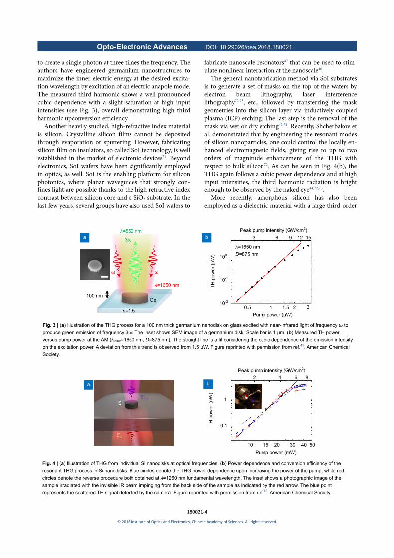
Another important advantage of high refractive index nanostructures is their large intrinsic nonlinear proper-ties, i.e. second and third order susceptibilities. Silicon and germanium are centrosymmetric materials lacking second-order susceptibility, however they possess large third-order nonlinearity. As such, silicon and germanium nanostructures hold great promise for strong enhance-ment of the nonlinear optical response. The fabrication process for germanium nanoantennas is very similar to metals, as germanium can be deposited with standard evaporation techniques. Recently, Grinblat et al.45 em-ployed this technique for fabrication of germanium an-tennas on borosilicate glass. Using such germanium nanoantennas, they obtained efficient Third Harmonic Generation (THG), 100 times larger than the THG from an unstructured germanium film (Fig.3(a)). THG is a nonlinear interaction when three photons are combined
Fig. 2 | (a) Angled SEM view of metamaterial showing Au nanorods. Inset demonstrates the propagation of fundamental and SHG waves. (b)
Far-field reflected SH spectra from a smooth Au surface (red line) and the nanorod metamaterial. Figure reproduced with permission from ref.41,
John Wiley and Sons.
a b
ω 2ω
2ω
2ω
1 μm
10-7
10-9
10-11
10-13
η(2ω
) (W -
1 )
meta TE meta TM Au film TM
300 600 900 1200 1500
Fund λ (nm)
Opto-Electronic Advances DOI: 10.29026/oea.2018.180021
180021‐4
© 2018 Institute of Optics and Electronics, Chinese Academy of Sciences. All rights reserved.
to create a single photon at three times the frequency. The authors have engineered germanium nanostructures to maximize the inner electric energy at the desired excita-tion wavelength by excitation of an electric anapole mode. The measured third harmonic shows a well pronounced cubic dependence with a slight saturation at high input intensities (see Fig. 3), overall demonstrating high third harmonic upconversion efficiency.
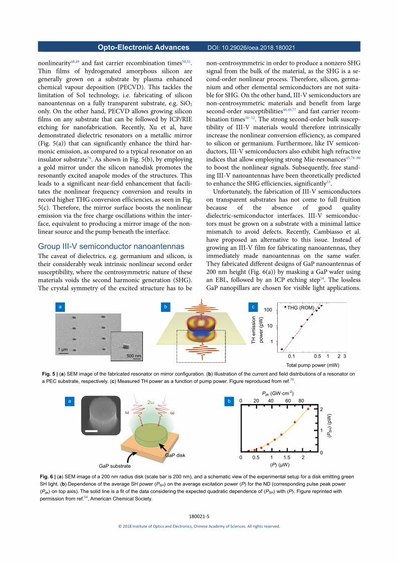
Another heavily studied, high-refractive index material is silicon. Crystalline silicon films cannot be deposited through evaporation or sputtering. However, fabricating silicon film on insulators, so called SoI technology, is well established in the market of electronic devices71. Beyond electronics, SoI wafers have been significantly employed in optics, as well. SoI is the enabling platform for silicon photonics, where planar waveguides that strongly con-fines light are possible thanks to the high refractive index contrast between silicon core and a SiO2 substrate. In the last few years, several groups have also used SoI wafers to
fabricate nanoscale resonators47 that can be used to stim-ulate nonlinear interaction at the nanoscale46.
The general nanofabrication method via SoI substrates is to generate a set of masks on the top of the wafers by electron beam lithography, laser interference lithography72,73, etc., followed by transferring the mask geometries into the silicon layer via inductively coupled plasma (ICP) etching. The last step is the removal of the mask via wet or dry etching47,74. Recently, Shcherbakov et al. demonstrated that by engineering the resonant modes of silicon nanoparticles, one could control the locally en-hanced electromagnetic fields, giving rise to up to two orders of magnitude enhancement of the THG with respect to bulk silicon72. As can be seen in Fig. 4(b), the THG again follows a cubic power dependence and at high input intensities, the third harmonic radiation is bright enough to be observed by the naked eye44,72,75.
More recently, amorphous silicon has also been employed as a dielectric material with a large third-order
Fig. 3 | (a) Illustration of the THG process for a 100 nm thick germanium nanodisk on glass excited with near-infrared light of frequency ω to
produce green emission of frequency 3ω. The inset shows SEM image of a germanium disk. Scale bar is 1 μm. (b) Measured TH power
versus pump power at the AM (λlaser=1650 nm, D=875 nm). The straight line is a fit considering the cubic dependence of the emission intensity
on the excitation power. A deviation from this trend is observed from 1.5 μW. Figure reprinted with permission from ref.45, American Chemical
Society.
Fig. 4 | (a) Illustration of THG from individual Si nanodisks at optical frequencies. (b) Power dependence and conversion efficiency of the
resonant THG process in Si nanodisks. Blue circles denote the THG power dependence upon increasing the power of the pump, while red
circles denote the reverse procedure both obtained at λ=1260 nm fundamental wavelength. The inset shows a photographic image of the
sample irradiated with the invisible IR beam impinging from the back side of the sample as indicated by the red arrow. The blue point
represents the scattered TH signal detected by the camera. Figure reprinted with permission from ref.72, American Chemical Society.
b
10-1
100
10-2
λ=1650 nm
D=875 nm
TH
po
we
r (p
W)
0.5 1 1.5 2 3
Pump power (μW)
3 6 9 12 15
Peak pump intensity (GW/cm2) a
100 nm
n=1.5
Ge
λ=1650 nm
ω ω
3ω
λ=550 nm
a 10-7
b
TH
po
we
r (n
W)
1
0.1
2 4 6 8
Peak pump intensity (GW/cm2)
10 15 20 30 40 50
Pump power (mW)
E3ω Si
Eω
Opto-Electronic Advances DOI: 10.29026/oea.2018.180021
180021‐5
© 2018 Institute of Optics and Electronics, Chinese Academy of Sciences. All rights reserved.
nonlinearity48,49 and fast carrier recombination times50,51. Thin films of hydrogenated amorphous silicon are generally grown on a substrate by plasma enhanced chemical vapour deposition (PECVD). This tackles the limitation of SoI technology, i.e. fabricating of silicon nanoantennas on a fully transparent substrate, e.g. SiO2 only. On the other hand, PECVD allows growing silicon films on any substrate that can be followed by ICP/RIE etching for nanofabrication. Recently, Xu et al, have demonstrated dielectric resonators on a metallic mirror (Fig. 5(a)) that can significantly enhance the third har-monic emission, as compared to a typical resonator on an insulator substrate76. As shown in Fig. 5(b), by employing a gold mirror under the silicon nanodisk promotes the resonantly excited anapole modes of the structures. This leads to a significant near-field enhancement that facili-tates the nonlinear frequency conversion and results in record higher THG conversion efficiencies, as seen in Fig. 5(c). Therefore, the mirror surface boosts the nonlinear emission via the free charge oscillations within the inter-face, equivalent to producing a mirror image of the non-linear source and the pump beneath the interface.
Group III-V semiconductor nanoantennas The caveat of dielectrics, e.g. germanium and silicon, is their considerably weak intrinsic nonlinear second order susceptibility, where the centrosymmetric nature of these materials voids the second harmonic generation (SHG). The crystal symmetry of the excited structure has to be
non-centrosymmetric in order to produce a nonzero SHG signal from the bulk of the material, as the SHG is a se-cond-order nonlinear process. Therefore, silicon, germa-nium and other elemental semiconductors are not suita-ble for SHG. On the other hand, III-V semiconductors are non-centrosymmetric materials and benefit from large second-order susceptibilities48,49,77 and fast carrier recom-bination times50–52. The strong second-order bulk suscep-tibility of III-V materials would therefore intrinsically increase the nonlinear conversion efficiency, as compared to silicon or germanium. Furthermore, like IV semicon-ductors, III-V semiconductors also exhibit high refractive indices that allow employing strong Mie-resonances45,78–80 to boost the nonlinear signals. Subsequently, free stand-ing III-V nanoantennas have been theoretically predicted to enhance the SHG efficiencies, significantly53.
Unfortunately, the fabrication of III-V semiconductors on transparent substrates has not come to full fruition because of the absence of good quality dielectric-semiconductor interfaces. III-V semiconduc-tors must be grown on a substrate with a minimal lattice mismatch to avoid defects. Recently, Cambiasso et al. have proposed an alternative to this issue. Instead of growing an III-V film for fabricating nanoantennas, they immediately made nanoantennas on the same wafer. They fabricated different designs of GaP nanoantennas of 200 nm height (Fig. 6(a)) by masking a GaP wafer using an EBL, followed by an ICP etching step54. The lossless GaP nanopillars are chosen for visible light applications.
Fig. 5 | (a) SEM image of the fabricated resonator on mirror configuration. (b) Illustration of the current and field distributions of a resonator on
a PEC substrate, respectively. (c) Measured TH power as a function of pump power. Figure reproduced from ref.76.
ba
1 μm
500 nm
c100 THG (ROM)
10
1 TH
em
issi
on
pow
er (
pW
)
0.1 0.5 1 2
Total pump power (mW)
Fig. 6 | (a) SEM image of a 200 nm radius disk (scale bar is 200 nm), and a schematic view of the experimental setup for a disk emitting green
SH light. (b) Dependence of the average SH power PSH on the average excitation power P for the ND (corresponding pulse peak power
Ppk on top axis). The solid line is a fit of the data considering the expected quadratic dependence of PSH with P . Figure reprinted with
permission from ref.54, American Chemical Society.
3
a
GaP disk
GaP substrate
ωω
2ω b 0 20 40 60 80
0 0.5 1 1.5 2
2
1
0
Ppk (GW·cm-2)
P (μW)
PS
H (
pW)
Opto-Electronic Advances DOI: 10.29026/oea.2018.180021
180021‐6
© 2018 Institute of Optics and Electronics, Chinese Academy of Sciences. All rights reserved.
The authors have shown that the manipulation of reso-nant modes at the surfaces of the dielectric structure can benefit the nonlinear SHG characteristics for a single nanostructure, in the visible range with a good conver-sion efficiency (see Fig. 6(b)).
It is well-known that confined electromagnetic fields inside the resonators can be significantly enhanced if a large refractive index contrast between the resonators and the substrate is present. Therefore, more efficient nonlin-ear optical signals can be generated if high-refractive in-dex nanoparticles are placed on oxide layers with low refractive indices. Indeed, the lack of a viable technology to produce high quality interfaces has been a barrier for reliable investigations and comprehensive understanding of compound semiconductor dielectric nanoantennas until very recently. GaAs nanoantennas have been re-cently fabricated on a glass substrate by Person et al.55. They implemented an epitaxial lift-off technique in con-junction with a water-bonding procedure to attach GaAs membrane (grown on a GaAs substrate) to a fused silica substrate. Using molecular beam epitaxy (MBE), a sacri-ficial layer of AlAs was grown on a GaAs substrate. On top of the AlAs layer a 1 μm film of GaAs was grown. Using the epitaxial lift-off procedure, the 1 μm GaAs film was transferred to a fused silica substrate. The transferred GaAs film was initially reduced to a thickness of ~150 nm by reactive ion etching (RIE). Disks were then patterned by EBL, followed by RIE. To this time, the authors only studied the forward and backward scattering from GaAs nanoparticles in the linear regime and did not explore the potential for nonlinear optics using such III-V structures on a transparent substrate.
Although, the abovementioned technique was the first of its kind, the low quality of resonators and the rough side-walls precluded to employing such nanopillars for applications in the nonlinear regime. Until recently, the full development of an III-V platform was hindered by the difficulty of fabricating monolithic shallow resonators in a way similar to the SoI platform. In particular, such opportunity was hindered by the shortcomings of wet selective oxidation of the epitaxial layers. To overcome these limitations, Gili et al. proposed an AlGaAs-based monolithic platform for nonlinear nanophotonics, as de-
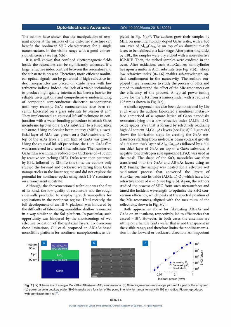
picted in Fig. 7(a)56. The authors grew their samples by MBE on non-intentionally doped GaAs wafer, with a 400 nm layer of Al0.18Ga0.82As on top of an aluminium-rich layer, to be oxidized at a later stage. After patterning disks by EBL, the samples were dry etched with a non-selective ICP-RIE. Then, the etched samples were oxidized in the oven. After oxidation, each Al0.18Ga0.82As nanocylinder lies upon a uniform AlOx substrate (see Fig. 7(b)), whose low refractive index (n=1.6) enables sub-wavelength op-tical confinement in the nanocavity. The authors em-ployed these resonators to study the process of SHG and aimed to understand the effect of the Mie-resonances on the efficiency of the process. A typical power-tuning curve for the SHG from a nanocylinder with a radius of 193 nm is shown in Fig. 7(c).
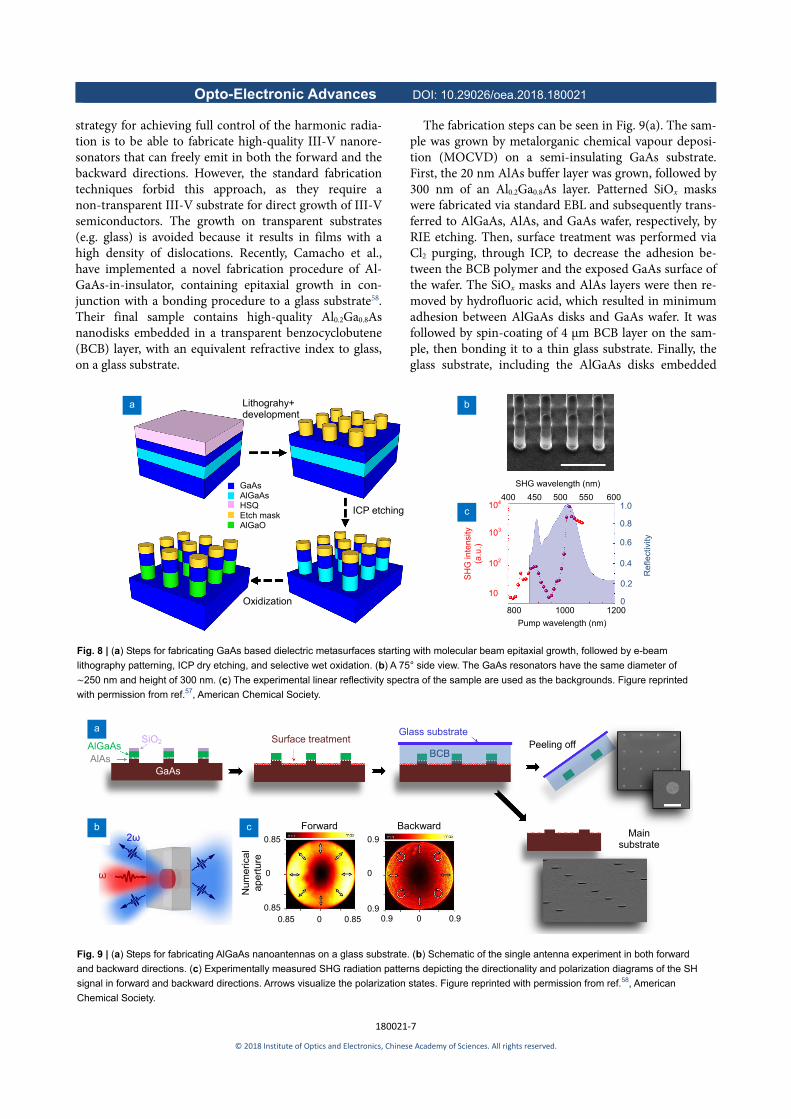
A similar approach has also been demonstrated by Liu et al, where the authors fabricated a nonlinear metasur-face comprised of a square lattice of GaAs nanodisks resonators lying on a low refractive index (AlxGa1–x)2O3 oxide spacer layer that is formed by selectively oxidizing high-Al content AlxGa1–xAs layers (see Fig. 8)57. Figure 8(a) shows the fabrication steps for creating the GaAs me-tasurfaces starting from molecular beam epitaxial growth of a 300 nm thick layer of Al0.85Ga0.15As followed by a 300 nm thick layer of GaAs on top of a GaAs substrate. A negative tone hydrogen silsesquioxane (HSQ) was used as the mask. The shape of the SiOx nanodisks was then transferred onto the GaAs and AlGaAs layers using an ICP. Finally, the sample was heated for a selective wet oxidization process that converted the layers of Al0.85Ga0.15As into its oxide (AlxGa1–x)2O3, which has a low refractive index of n =1.6, see Fig. 8(b). Again, the authors studied the process of SHG from such metasurfaces and tuned the incident wavelength to optimise the SHG con-version efficiency, which peaks at the spectral position of the Mie-resonances, aligned with the maximum of the reflectivity, shown in Fig. 8(c).
Both approaches above for fabricating AlGaAs and GaAs on an insulator, respectively, led to efficiencies that exceed ~10-5. However, in both cases the antennas are sitting on a handle GaAs wafer that is not transparent in the visible range, and therefore limits the nonlinear emis-sion in the forward or backward direction. An important
Fig. 7 | (a) Schematics of a single Monolithic AlGaAs-on-AlOx nanoantenna. (b) Scanning-electron-microscope picture of a part of the array and
(c) power curve in Log/Log scale. SHG intensity as a function of the pump intensity for nanoantenna with 193 nm radius. Figure reproduced
with permission from ref.56.
c
1 μm
b 400 nm 90 nm
1 μm
90 nm
AlOx
GaAs
AlOx gradient
AlOx gradient Al0.18Ga0.82As
a
0.01
Incident power (mW)
0.1 1
108
107
106
105
104
SH
G (
cts/
s)
Increasing Pin Decreasing Pin Quadratic fit
Opto-Electronic Advances DOI: 10.29026/oea.2018.180021
180021‐7
© 2018 Institute of Optics and Electronics, Chinese Academy of Sciences. All rights reserved.
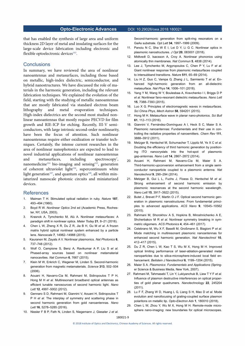
strategy for achieving full control of the harmonic radia-tion is to be able to fabricate high-quality III-V nanore-sonators that can freely emit in both the forward and the backward directions. However, the standard fabrication techniques forbid this approach, as they require a non-transparent III-V substrate for direct growth of III-V semiconductors. The growth on transparent substrates (e.g. glass) is avoided because it results in films with a high density of dislocations. Recently, Camacho et al., have implemented a novel fabrication procedure of Al-GaAs-in-insulator, containing epitaxial growth in con-junction with a bonding procedure to a glass substrate58. Their final sample contains high-quality Al0.2Ga0.8As nanodisks embedded in a transparent benzocyclobutene (BCB) layer, with an equivalent refractive index to glass, on a glass substrate.
The fabrication steps can be seen in Fig. 9(a). The sam-ple was grown by metalorganic chemical vapour deposi-tion (MOCVD) on a semi-insulating GaAs substrate. First, the 20 nm AlAs buffer layer was grown, followed by 300 nm of an Al0.2Ga0.8As layer. Patterned SiOx masks were fabricated via standard EBL and subsequently trans-ferred to AlGaAs, AlAs, and GaAs wafer, respectively, by RIE etching. Then, surface treatment was performed via Cl2 purging, through ICP, to decrease the adhesion be-tween the BCB polymer and the exposed GaAs surface of the wafer. The SiOx masks and AlAs layers were then re-moved by hydrofluoric acid, which resulted in minimum adhesion between AlGaAs disks and GaAs wafer. It was followed by spin-coating of 4 μm BCB layer on the sam-ple, then bonding it to a thin glass substrate. Finally, the glass substrate, including the AlGaAs disks embedded
Fig. 8 | (a) Steps for fabricating GaAs based dielectric metasurfaces starting with molecular beam epitaxial growth, followed by e-beam
lithography patterning, ICP dry etching, and selective wet oxidation. (b) A 75° side view. The GaAs resonators have the same diameter of
∼250 nm and height of 300 nm. (c) The experimental linear reflectivity spectra of the sample are used as the backgrounds. Figure reprinted
with permission from ref.57, American Chemical Society.
Fig. 9 | (a) Steps for fabricating AlGaAs nanoantennas on a glass substrate. (b) Schematic of the single antenna experiment in both forward
and backward directions. (c) Experimentally measured SHG radiation patterns depicting the directionality and polarization diagrams of the SH
signal in forward and backward directions. Arrows visualize the polarization states. Figure reprinted with permission from ref.58, American
Chemical Society.
a b
c
GaAs AlGaAs HSQ Etch mask AlGaO
Lithograhy+ development
ICP etching
Oxidization
SHG wavelength (nm)
400 500 600 104
103
102
10
SH
G in
tens
ity
(a.u
.)
800 1000 1200
Pump wavelength (nm)
450 550 1.0
0.8
0.6
0.4
0.2
0
Ref
lect
ivity
a SiO2
b c
AlGaAs AlAs
GaAs
Surface treatmentGlass substrate
BCBPeeling off
Main substrate
2ω
ω
Forward Backward
Nu
me
rical
ap
ertu
re
0.85
0
0.85
0.9
0
0.9 0.85 0 0.85 0.9 0.90

Opto-Electronic Advances DOI: 10.29026/oea.2018.180021
180021‐8
© 2018 Institute of Optics and Electronics, Chinese Academy of Sciences. All rights reserved.
within the BCB layer, was peeled off from the main GaAs wafer58. The electron microscopy images of AlGaAs disks and the pillar bases remaining on the original substrate can be seen on the right-hand-side of Fig. 9(a).
This technique allows not only obtaining efficient SHG, but also enabling the control of directionality and full characterisation of the polarization of the nonlinear emission in both forward and backward direction, as shown in Fig. 9(b). Figure 9(c) demonstrates the experi-mentally measured polarization states in both directions, where vector-beam formation at the SH frequency takes place. Interestingly, in the experiment, one can observe nearly perfect radial polarization of the SH in the forward direction. It is worth mentioning that GaAs family reso-nators are capable to exhibit nonlinear interaction beyond SHG and THG, e.g. sum-frequency generation, four-wave mixing, etc81–83. This is a unique opportunity that enables nonlinear mixing for wide range of applications such as communications and quantum optics.
Hybrid nanoantennas In the previous sections, it was shown that metallic nanoantennas are a good alternative for nonlinear nanophotonics due to the strong local field enhancement in such systems. Subsequently, it was discussed that high-index dielectric nanoparticles could provide new avenues for the study of nonlinear effects due to their very low losses and large light scattering efficiency. In the meanwhile, some research works have demonstrated that combining the advantages of the metal and dielec-tric/semiconductor approaches can push the conversion efficiency to even larger values. Various types of hybrid nanoantennas, consisting of metallic resonators embed-ded in dielectric and semiconductor media or vice-versa, have been proposed and realized in the recent years. In-dium tin oxide (ITO) particles within Au nanoantennas19,20,84–86, is an example of such efforts with promising results. As can be seen in Fig. 10(a), Aouani et al., have obtained a ground breaking 106 fold enhance-ment of THG from an individual ITO nanoparticle, upon being decorated by a gold antenna20. Subsequently, there
have been several publications, in which the localised fields in nanoscale gaps width of metallic antennas have been studied, through Landau damping87, hyperbolic co-sine catenary function88, etc.
Similarly, several orders of magnitude increase in nonlinear conversion efficiencies of second- and third-order effects have been demonstrated in plasmonic particles placed on top of nonlinear GaAs substrates10, nanopatterned plasmonic films filled with GaAs89, metal/dielectric core-shell nanoparticles90, plasmonic ring filled by concentric Lithium Niobate91, silicon92, AlGaAs93 disks, etc. It was also shown in linear hybrid nanostruc-tures that plasmonic-Mie mode hybridization can give rise to high radiation directivity94–96. The fabrication technique for hybrid nanostructuring is generally a com-bination of the techniques discussed above, consisting of multiple EBL steps, requiring precise alignment of every subsequent mask to the previous steps.
Layered materials Layered materials, known as 2D materials and their hetrostructures, are a rapidly growing class of materials with the ability to emit and detect light at different wave-length ranges97,98. These materials possess different band gaps and a large range of conductivities. Graphene is the most studied 2D material that has no band gap and be-haves like a metal. On the other hand other 2D materials, such as WS2, MoS2, MoSe2 and WSe2 have semiconduct-ing band gaps on the order of 1–2.5 eV, and hexagonal boron nitride (h-BN) with a wide band gap on the order of 6 eV99. Very recently, 2D materials have been employed for enhancing nonlinear efficiencies at nanoscale97. One of the common issues of 2D materials is that a single monolayer only slightly perturbs the cavity mode. Thus, the cavity is formed by another linear material, while 2D materials only provide the required nonlinearity. For ex-ample, by using graphene and hBN layered structures it is possible to create hyperbolic metamaterials100,101. Thereby, 2D materials offer an important alternative for enhancing the nonlinear optical interaction102. Chemical vapor dep-osition (CVD) technique is the most employed method
Fig. 10 | Measured THG intensity from (a) an isolated ITO particle (left) versus (b) hybridized ITO-Au antenna. Insets show SEM image of
an antenna for each case. Figure reproduced from ref.20.
a
TH
G in
ten
sity
(p
hoto
ns·s
-1·μ
m-2
)
b
TH
G in
ten
sity
(1
06 p
hoto
ns·s
-1·μ
m-2
)
ITO dot
50 nm
E E
4
3
2
1
0
470 480 490 500 510 520 530
Wavelength (nm)
7
6
5
4
3
2
1
0
470 480 490 500 510 520 530
Wavelength (nm)
100 nm
ITO
Opto-Electronic Advances DOI: 10.29026/oea.2018.180021
180021‐9
© 2018 Institute of Optics and Electronics, Chinese Academy of Sciences. All rights reserved.
that has enabled the synthesis of large area and uniform thickness 2D layer of metal and insulating surfaces for the large-scale device fabrication including electronic and flexible optoelectronic devices103.
Conclusions In summary, we have reviewed the area of nonlinear nanoantennas and metasurfaces, including those based on metallic, high-index dielectric, semiconductor, and hybrid nanostructures. We have discussed the role of ma-terials in the harmonic generation, including the relevant fabrication techniques. We explained the evolution of the field, starting with the studying of metallic nanoantennas that are mostly fabricated via standard electron beam lithography and metal evaporation techniques. High-index dielectrics are the second most studied non-linear nanoantennas that mostly require PECVD for film growth and RIE-ICP for etching. Recently, III-V semi-conductors, with large intrinsic second-order nonlinearity, have been the focus of attention. Such nonlinear nanoantennas require either oxidization or transfer tech-niques. Certainly, the intense current researches in the area of nonlinear nanophotonics are expected to lead to novel industrial applications of nonlinear nanoantennas and metasurfaces, including spectroscopy7, nanomedicine104 bio-imaging and sensing105, generation of coherent ultraviolet light106, supercontinuum white light generation107, and quantum optics108, all within min-iaturized nanoscale photonic circuits and miniaturized devices.
References 1. Maiman T H. Stimulated optical radiation in ruby. Nature 187,
493–494 (1960).
2. Boyd R W. Nonlinear Optics 2nd ed (Academic Press, Roches-
ter, NY, USA, 2003).
3. Krasnok A, Tymchenko M, Alù A. Nonlinear metasurfaces: A
paradigm shift in nonlinear optics. Mater Today 21, 8–21 (2018).
4. Chen L W, Zheng X R, Du Z R, Jia B H, Gu M et al. A frozen
matrix hybrid optical nonlinear system enhanced by a particle
lens. Nanoscale 7, 14982–14988 (2015).
5. Kauranen M, Zayats A V. Nonlinear plasmonics. Nat Photonics 6,
737–748 (2012).
6. Wolf O, Campione S, Benz A, Ravikumar A P, Liu S et al.
Phased-array sources based on nonlinear metamaterial
nanocavities. Nat Commun 6, 7667 (2015).
7. Klein M W, Enkrich C, Wegener M, Linden S. Second-harmonic
generation from magnetic metamaterials. Science 313, 502–504
(2006).
8. Aouani H, Navarro-Cia M, Rahmani M, Sidiropoulos T P H,
Hong M H et al. Multiresonant broadband optical antennas as
efficient tunable nanosources of second harmonic light. Nano
Lett 12, 4997–5002 (2012).
9. Gennaro S D, Rahmani M, Giannini V, Aouani H, Sidiropoulos T
P H et al. The interplay of symmetry and scattering phase in
second harmonic generation from gold nanoantennas. Nano
Lett 16, 5278–5285 (2016).
10. Niesler F B P, Feth N, Linden S, Niegemann J, Gieseler J et al.
Second-harmonic generation from split-ring resonators on a
GaAs substrate. Opt Lett 34, 1997–1999 (2009).
11. Panoiu N C, Sha W E I, Lei D Y, Li G C. Nonlinear optics in
plasmonic nanostructures. J Opt 20, 083001 (2018).
12. Midtvedt D, Isacsson A, Croy A. Nonlinear phononics using
atomically thin membranes. Nat Commun 5, 4838 (2014).
13. Lee J, Tymchenko M, Argyropoulos C, Chen P Y, Lu F et al.
Giant nonlinear response from plasmonic metasurfaces coupled
to intersubband transitions. Nature 511, 65–69 (2014).
14. Liu H Z, Guo C, Vampa G, Zhang J L, Sarmiento T et al. En-
hanced high-harmonic generation from an all-dielectric
metasurface. Nat Phys 14, 1006–101 (2018).
15. Yang Y M, Wang W Y, Boulesbaa A, Kravchenko I I, Briggs D P
et al. Nonlinear fano-resonant dielectric metasurfaces. Nano Lett
15, 7388–7393 (2015).
16. Luo X G. Principles of electromagnetic waves in metasurfaces.
Sci China Phys, Mech Astron 58, 594201 (2015).
17. Hong M H. Metasurface wave in planar nano-photonics. Sci Bull
61, 112–113 (2016).
18. Giannini V, Fernández-Domínguez A I, Heck S C, Maier S A.
Plasmonic nanoantennas: Fundamentals and their use in con-
trolling the radiative properties of nanoemitters. Chem Rev 111,
3888–3912 (2011).
19. Metzger B, Hentschel M, Schumacher T, Lippitz M, Ye X C et al.
Doubling the efficiency of third harmonic generation by position-
ing ITO nanocrystals into the hot-spot of plasmonic
gap-antennas. Nano Lett 14, 2867–2872 (2014).
20. Aouani H, Rahmani M, Navarro-Cía M, Maier S A.
Third-harmonic-upconversion enhancement from a single semi-
conductor nanoparticle coupled to a plasmonic antenna. Nat
Nanotechnol 9, 290–294 (2014).
21. Metzger B, Gui L L, Fuchs J, Floess D, Hentschel M et al.
Strong enhancement of second harmonic emission by
plasmonic resonances at the second harmonic wavelength.
Nano Lett 15, 3917–3922 (2015).
22. Butet J, Brevet P F, Martin O J F. Optical second harmonic gen-
eration in plasmonic nanostructures: From fundamental princi-
ples to advanced applications. ACS Nano 9, 10545–10562
(2015).
23. Rahmani M, Shorokhov A S, Hopkins B, Miroshnichenko A E,
Shcherbakov M R et al. Nonlinear symmetry breaking in sym-
metric oligomers. ACS Photonics 4, 454–461 (2017).
24. Celebrano M, Wu X F, Baselli M, Großmann S, Biagioni P et al.
Mode matching in multiresonant plasmonic nanoantennas for
enhanced second harmonic generation. Nat Nanotechnol 10,
412–417 (2015).
25. Du Z R, Chen L W, Kao T S, Wu M X, Hong M H. Improved
optical limiting performance of laser-ablation-generated metal
nanoparticles due to silica-microsphere-induced local field en-
hancement. Beilstein J Nanotechnol 6, 1199–1204 (2015).
26. Maier S A. Plasmonics: Fundamentals and Applications (Spring-
er Science & Business Media, New York, 2007).
27. Rahmani M, Tahmasebi T, Lin Y, Lukiyanchuk B, Liew T Y F et al.
Influence of plasmon destructive interferences on optical proper-
ties of gold planar quadrumers. Nanotechnology 22, 245204
(2011).
28. Lu F F, Zhang W D, Huang L G, Liang S H, Mao D et al. Mode
evolution and nanofocusing of grating-coupled surface plasmon
polaritons on metallic tip. Opto-Electron Adv 1, 180010 (2018).
29. Chen L W, Zhou Y, Wu M X, Hong M H. Remote-mode micro-
sphere nano-imaging: new boundaries for optical microscopes.
Opto-Electronic Advances DOI: 10.29026/oea.2018.180021
180021‐10
© 2018 Institute of Optics and Electronics, Chinese Academy of Sciences. All rights reserved.
Opto-Electron Adv 1, 170001 (2018).
30. Rahmani M, Luk'yanchuk B, Hong M H. Fano resonance in
novel plasmonic nanostructures. Laser Photonics Rev 7,
329–349 (2013).
31. Zhang W Q, Rahmani M, Niu W X, Ravaine S, Hong M H et al.
Tuning interior nanogaps of double-shelled Au/Ag nanoboxes for
surface-enhanced raman scattering. Sci Rep 5, 8382 (2015).
32. Della Picca F, Berte R, Rahmani M, Albella P, Bujjamer J M et al.
Tailored hypersound generation in single plasmonic
nanoantennas. Nano Lett 16, 1428–1434 (2016).
33. Kuznetsov A I, Miroshnichenko A E, Fu Y H, Viswanathan V,
Rahmani M et al. Split-ball resonator as a three-dimensional an-
alogue of planar split-rings. Nat Commun 5, 3104 (2014).
34. Hanke T, Cesar J, Knittel V, Trügler A, Hohenester U et al. Tai-
loring spatiotemporal light confinement in single plasmonic
nanoantennas. Nano Lett 12, 992–996 (2012).
35. Fernandez-Garcia R, Rahmani M, Hong M H, Maier S A,
Sonnefraud Y. Use of a gold reflecting-layer in optical antenna
substrates for increase of photoluminescence enhancement.
Opt Express 21, 12552–12561 (2013).
36. Yoxall E, Navarro-Cía M, Rahmani M, Maier S A, Phillips C C.
Widely tuneable scattering-type scanning near-field optical mi-
croscopy using pulsed quantum cascade lasers. Appl Phys Lett
103, 213110 (2013).
37. Geraci G, Hopkins B, Miroshnichenko A E, Erkihun B, Neshev D
N et al. Polarisation-independent enhanced scattering by tailor-
ing asymmetric plasmonic systems. Nanoscale 8, 6021–6027
(2016).
38. Rifat A A, Rahmani M, Xu L, Miroshnichenko A E. Hybrid
metasurface based tunable near-perfect absorber and
plasmonic sensor. Materials 11, 1091 (2018).
39. Franken P, Hill A E, Peters C W, Weinreich G. Generation of
optical harmonics. Phys Rev Lett 7, 118–119 (1961).
40. Segovia P, Marino G, Krasavin A V, Olivier N, Wurtz G A et al.
Hyperbolic metamaterial antenna for second-harmonic genera-
tion tomography. Opt Express 23, 30730–30738 (2015).
41. Marino G, Segovia P, Krasavin A V, Ginzburg P, Olivier N et al.
Second-harmonic generation from hyperbolic plasmonic
nanorod metamaterial slab. Laser Photonics Rev 12, 1700189
(2018).
42. Wang P, Krasavin A V, Nasir M E, Dickson W, Zayats A V. Reac-
tive tunnel junctions in electrically driven plasmonic nanorod
metamaterials. Nat Nanotechnol 13, 159–164 (2018).
43. Dickson W, Beckett S, McClatchey C, Murphy A, O'Connor D et
al. Hyperbolic polaritonic crystals based on nanostructured
nanorod metamaterials. Adv Mater 27, 5974–5980 (2015).
44. Shorokhov A S, Melik-Gaykazyan E V, Smirnova D A, Hopkins B,
Chong K E et al. Multifold enhancement of third-harmonic gen-
eration in dielectric nanoparticles driven by magnetic fano reso-
nances. Nano Lett 16, 4857–4861 (2016).
45. Grinblat G, Li Y, Nielsen M P, Oulton R F, Maier S A. Enhanced
third harmonic generation in single germanium nanodisks excit-
ed at the anapole mode. Nano Lett 16, 4635–4640 (2016).
46. Nielsen M P, Lafone L, Rakovich A, Sidiropoulos T P H,
Rahmani M et al. Adiabatic nanofocusing in hybrid gap plasmon
waveguides on the silicon-on-insulator platform. Nano Lett 16,
1410–1414 (2016).
47. Caldarola M, Albella P, Cortés E, Rahmani M, Roschuk T et al.
Non-plasmonic nanoantennas for surface enhanced spectros-
copies with ultra-low heat conversion. Nat Commun 6, 7915
(2015).
48. Ikeda K, Shen Y M, Fainman Y. Enhanced optical nonlinearity in
amorphous silicon and its application to waveguide devices. Opt
Express 15, 17761–17771 (2007).
49. Gai X, Choi D Y, Luther-Davies B. Negligible nonlinear absorp-
tion in hydrogenated amorphous silicon at 1.55 μm for ultra-fast
nonlinear signal processing. Opt Express 22, 9948–9958
(2014).
50. Fauchet P M, Hulin D. Ultrafast carrier relaxation in hydrogen-
ated amorphous silicon. J Opt Sci Am B 6, 1024–1029 (1989).
51. Sheik-Bahae M, Said A A, Wei T H, Hagan D J, Van Stryland E
W. Sensitive measurement of optical nonlinearities using a sin-
gle beam. IEEE J of Quantum Electron 26, 760–769 (1990).
52. Boyd G D, Patel C K N. Enhancement of optical second‐
harmonic generation (SHG) by reflection phase matching in Zns
and GaAs. Appl Phys Lett 8, 313–315 (1966).
53. Carletti L, Locatelli A, Stepanenko O, Leo G, De Angelis C. En-
hanced second-harmonic generation from magnetic resonance
in ALGaAs nanoantennas. Opt Express 23, 26544–26550
(2015).
54. Cambiasso J, Grinblat G, Li Y, Rakovich A, Cortés E et al.
Bridging the gap between dielectric nanophotonics and the visi-
ble regime with effectively lossless gallium phosphide antennas.
Nano Lett 17, 1219–1225 (2017).
55. Person S, Jain M, Lapin Z, Sáenz J J, Wicks G et al. Demon-
stration of zero optical backscattering from single nanoparticles.
Nano Lett 13, 1806–1809 (2013).
56. Gili V F, Carletti L, Locatelli A, Rocco D, Finazzi M et al. Mono-
lithic ALGaAs second-harmonic nanoantennas. Opt Express 24,
15965–15971 (2016).
57. Liu S, Sinclair M B, Saravi S, Keeler G A, Yang Y M et al. Res-
onantly enhanced second-harmonic generation using III–V
semiconductor all-dielectric metasurfaces. Nano Lett 16,
5426–5432 (2016).
58. Camacho-Morales R, Rahmani M, Kruk S, Wang L, Xu L et al.
Nonlinear generation of vector beams from ALGaAs
nanoantennas. Nano Lett 16, 7191–7197 (2016).
59. Shcherbakov M R, Shorokhov A S, Neshev D N, Hopkins B,
Staude I et al. Nonlinear interference and tailorable
third-harmonic generation from dielectric oligomers. ACS Pho-
tonics 2, 578–582 (2015).
60. Della Valle G, Hopkins B, Ganzer L, Stoll T, Rahmani M et al.
Nonlinear anisotropic dielectric metasurfaces for ultrafast
nanophotonics. ACS Photonics 4, 2129–2136 (2017).
61. Chen S M, Rahmani M, Li K F, Miroshnichenko A, Zentgraf T et
al. Third harmonic generation enhanced by multipolar interfer-
ence in complementary silicon metasurfaces. ACS Photonics 5,
1671–1675 (2018).
62. Nemati A, Wang Q, Hong M H, Teng J H. Tunable and reconfig-
urable metasurfaces and metadevices. Opto-Electron Adv 1,
180009 (2018).
63. Grinblat G, Li Y, Nielsen M P, Oulton R F, Maier S A. Degenerate
four-wave mixing in a multiresonant germanium nanodisk. ACS
Photonics 4, 2144–2149 (2017).
64. Chen L M, Jiang X F, Guo Z M, Zhu H, Kao T S et al. Tuning
optical nonlinearity of laser-ablation-synthesized silicon nano-
particles via doping concentration. J Nanomater 2014, 652829
(2014).
65. Wang L, Kruk S, Xu L, Rahmani M, Smirnova D et al. Shaping
the third-harmonic radiation from silicon nanodimers. Nanoscale
9, 2201–2206 (2017).
66. Makarov S V, Petrov M I, Zywietz U, Milichko V, Zuev D et al.
Opto-Electronic Advances DOI: 10.29026/oea.2018.180021
180021‐11
© 2018 Institute of Optics and Electronics, Chinese Academy of Sciences. All rights reserved.
Efficient second-harmonic generation in nanocrystalline silicon
nanoparticles. Nano Lett 17, 3047–3053 (2017).
67. Melik-Gaykazyan E V, Kruk S S, Camacho-Morales R, Xu L,
Rahmani M et al. Selective third-harmonic generation by struc-
tured light in mie-resonant nanoparticles. ACS Photonics 5,
728–733 (2018).
68. Tong W Y, Gong C, Liu X J, Yuan S, Huang Q Z et al. Enhanced
third harmonic generation in a silicon metasurface using trapped
mode. Opt Express 24, 19661–19670 (2016).
69. Kuznetsov A I, Miroshnichenko A E, Fu Y H, Zhang J B,
Luk’yanchuk B. Magnetic light. Sci Rep 2, 492 (2012).
70. Smirnova D, Kivshar Y S. Multipolar nonlinear nanophotonics.
Optica 3, 1241–1255 (2016).
71. Lu B H, Lan H B, Liu H Z. Additive manufacturing frontier: 3D
printing electronics. Opto-Electron Adv 1, 170004 (2018).
72. Shcherbakov M R, Neshev D N, Hopkins B, Shorokhov A S,
Staude I et al. Enhanced third-harmonic generation in silicon
nanoparticles driven by magnetic response. Nano Lett 14,
6488–6492 (2014).
73. Choi W K, Liew T H, Dawood M K, Smith H I, Thompson C V et
al. Synthesis of silicon nanowires and nanofin arrays using in-
terference lithography and catalytic etching. Nano Lett 8,
3799–3802 (2008).
74. Rahmani M, Xu L, Miroshnichenko A E, Komar A, Camacho-
Morales R et al. Reversible thermal tuning of all-dielectric
metasurfaces. Adv Funct Mater 27, 1700580 (2017).
75. Shcherbakov M R, Vabishchevich P P, Shorokhov A S, Chong K
E, Choi D Y et al. Ultrafast all-optical switching with magnetic
resonances in nonlinear dielectric nanostructures. Nano Lett 15,
6985–6990 (2015).
76. Xu L, Rahmani M, Kamali K Z, Lamprianidis A, Ghirardini L et al.
Boosting third-harmonic generation by a mirror-enhanced
anapole resonator. Light: Sci Appl 7, 44 (2018).
77. Löchner F J, Fedotova A N, Liu S, Keeler G A, Peake G M et al.
Polarization-dependent second harmonic diffraction from reso-
nant gaas metasurfaces. ACS Photonics 5, 1786–1793 (2018).
78. Mie G. Beiträge zur optik trüber medien, speziell kolloidaler
metallösungen. Ann Phys 330, 377–445 (1908).
79. Debye P. Der lichtdruck auf kugeln von beliebigem material. Ann
Phys 335, 57–136 (1909).
80. Xu L, Rahmani M, Smirnova D, Zangeneh Kamali K, Zhang G Q
et al. Highly-efficient longitudinal second-harmonic generation
from doubly-resonant algaas nanoantennas. Photonics 5, 29
(2018).
81. Liu S, Vabishchevich P P, Vaskin A, Reno J L, Keeler G A et al.
An all-dielectric metasurface as a broadband optical frequency
mixer. Nat Commun 9, 2507 (2018).
82. Carletti L, Marino G, Ghirardini L, Gili V F, Rocco D et al. Non-
linear goniometry by second-harmonic generation in algaas
nanoantennas. ACS Photonics 5, 4386–4392 (2018).
83. Shcherbakov M R, Liu S, Zubyuk V V, Vaskin A, Vabishchevich
P P et al. Ultrafast all-optical tuning of direct-gap semiconductor
metasurfaces. Nat Commun 8, 17 (2017).
84. Aouani H, Navarro-Cía M, Rahmani M, Maier S A. Unveiling the
origin of third harmonic generation in hybrid ITO–plasmonic
crystals. Adv Opt Mater 3, 1059–1065 (2015).
85. Linnenbank H, Grynko Y, Förstner J, Linden S. Second harmon-
ic generation spectroscopy on hybrid plasmonic/dielectric
nanoantennas. Light: Sci Appl 5, e16013 (2016).
86. Abb M, Albella P, Aizpurua J, Muskens O. All-optical control of a
single plasmonic nanoantenna–ITO hybrid. Nano Lett 11,
2457–2463 (2011).
87. Khurgin J, Tsai W Y, Tsai D P, Sun G. Landau damping and limit
to field confinement and enhancement in plasmonic dimers.
ACS Photonics 4, 2871–2880 (2017).
88. Pu M B, Guo Y H, Li X, Ma X L, Luo X G. Revisitation of extraor-
dinary young’s interference: From catenary optical fields to
spin-orbit interaction in metasurfaces. ACS Photonics 5,
3198–3204 (2018).
89. Fan W J, Zhang S, Panoiu N C, Abdenour A, Krishna S et al.
Second harmonic generation from a nanopatterned isotropic
nonlinear material. Nano Lett 6, 1027–1030 (2006).
90. Pu Y, Grange R, Hsieh C L, Psaltis D. Nonlinear optical proper-
ties of core-shell nanocavities for enhanced second-harmonic
generation. Phys Rev Lett 104, 207402 (2010).
91. Lehr D, Reinhold J, Thiele I, Hartung H, Dietrich K et al. En-
hancing second harmonic generation in gold nanoring resona-
tors filled with lithium niobate. Nano Lett 15, 1025–1030 (2015).
92. Shibanuma T, Grinblat G, Albella P, Maier S A. Efficient third
harmonic generation from metal–dielectric hybrid nanoantennas.
Nano Lett 17, 2647–2651 (2017).
93. Gili V F, Ghirardini L, Rocco D, Marino G, Favero I et al. Met-
al–dielectric hybrid nanoantennas for efficient frequency conver-
sion at the anapole mode. Beilstein J Nanotechnol 9,
2306–2314 (2018).
94. Decker M, Pertsch T, Staude I. Strong coupling in hybrid met-
al–dielectric nanoresonators. Philos Trans Roy Soc A: Math,
Phys Eng Sci 375, 20160312 (2017).
95. Guo R, Rusak E, Staude I, Dominguez J, Decker M et al. Multi-
polar coupling in hybrid metal–dielectric metasurfaces. ACS
Photonics 3, 349–353 (2016).
96. Rusak E, Staude I, Decker M, Sautter J, Miroshnichenko A E et
al. Hybrid nanoantennas for directional emission enhancement.
Appl Phys Lett 105, 221109 (2014).
97. Xia F N, Wang H, Xiao D, Dubey M, Ramasubramaniam A.
Two-dimensional material nanophotonics. Nat Photonics 8, 899
(2014).
98. Zheng X R, Jia B H, Chen X, Gu M. In situ third-order non-linear
responses during laser reduction of graphene oxide thin films
towards on-chip non-linear photonic devices. Adv Mater 26,
2699–2703 (2014).
99. Fryett T, Zhan A, Majumdar A. Cavity nonlinear optics with lay-
ered materials. Nanophotonics 7, 69 (2017).
100. Dai S, Ma Q, Liu M K, Andersen T, Fei Z et al. Graphene on
hexagonal boron nitride as a tunable hyperbolic metamaterial.
Nat Nanotechnol 10, 682–686 (2015).
101. Kumar A, Low T, Fung K H, Avouris P, Fang N X. Tunable
light–matter interaction and the role of hyperbolicity in
graphene–hbn system. Nano Lett 15, 3172–3180 (2015).
102. Poddubny A, Iorsh I, Belov P, Kivshar Y. Hyperbolic
metamaterials. Nat Photonics 7, 948–957 (2013).
103. Gupta A, Sakthivel T, Seal S. Recent development in 2D materi-
als beyond graphene. Prog Mater Sci 73, 44–126 (2015).
104. Geissbuehler M, Bonacina L, Shcheslavskiy V, Bocchio N L,
Geissbuehler S et al. Nonlinear correlation spectroscopy
(NLCS). Nano Lett 12, 1668–1672 (2012).
105. DaCosta M V, Doughan S, Han Y, Krull U J. Lanthanide
upconversion nanoparticles and applications in bioassays and
bioimaging: A review. Anal Chim Acta 832, 1–33 (2014).
106. Makarov S V, Tsypkin A N, Voytova T A, Milichko V A, Mukhin I S
et al. Self-adjusted all-dielectric metasurfaces for deep ultravio-
let femtosecond pulse generation. Nanoscale 8, 17809–17814
Opto-Electronic Advances DOI: 10.29026/oea.2018.180021
180021‐12
© 2018 Institute of Optics and Electronics, Chinese Academy of Sciences. All rights reserved.
(2016).
107. Krasavin A V, Ginzburg P, Wurtz G A, Zayats A V.
Nonlocality-driven supercontinuum white light generation in
plasmonic nanostructures. Nat Commun 7, 11497 (2016).
108. Barz S, Cronenberg G, Zeilinger A, Walther P. Heralded genera-
tion of entangled photon pairs. Nat Photonics 4, 553–556
(2010).
Acknowledgements The authors acknowledge the financial support provided by the Australian Research Council (ARC) and participation in the Erasmus Mundus NANOPHI project, contract number 2013 5659/002-001. M. R. sincerely appreciates funding from an ARC Discovery Early Career Research Fellow-ship (DE170100250) and funding from the Australian Nanotechnology Network. M. R. and A. E. M. appreciate a funding from Australia–Germany Joint Research Cooperation Scheme. The work of A. E. M. was supported by a UNSW Scientia Fellowship. G. L. and V. F. G. acknowledge funding from SEAM Labex (PANAMA project)”. A. V. Z., S. A. M. and R.O. acknowledge the funding provided by the EPSRC Reactive Plasmonics Programme (EP/M013812/1), the ONR Global, the Leverhulme Trust, the Royal Society (UF150542). A. V. Z. acknowledges support from the Royal Society and the Wolfson Foundation. S. A. M. appreciates supports from the Lee-Lucas Chair
in Physics and acknowledges the DFG Cluster of Excellence Nanoinitiative Munich (NIM), and the Solar Technologies Go Hybrid (SOLTEC) projects. I. S. gratefully acknowledges financial support by the German Research Foun-dation (STA 1426/2-1) and the Thuringian State Government within its ProExcellence initiative (APC2020). I. B. acknowledges the support of the U.S. Department of Energy, Office of Basic Energy Sciences, Division of Materials Sciences and Engineering. I. B., I. S. and D. N. N. acknowledge the support of the Center for Integrated Nanotechnologies, an Office of Science User Facil-ity operated for the U.S. Department of Energy (DOE) Office of Sci-ence. Sandia National Laboratories is a multi-mission laboratory managed and operated by National Technology and Engineering Solutions of Sandia, LLC, a wholly owned subsidiary of Honeywell International, Inc., for the U.S. Department of Energy’s National Nuclear Security Administration under contract DE-NA0003525. This paper describes objective technical results and analysis. Any subjective views or opinions that might be expressed in the paper do not necessarily represent the views of the U.S. Department of En-ergy or the United States Government. The authors acknowledge the use of the Australian National Fabrication Facility (ANFF), the ACT Node.
Competing interests The authors declare no competing financial interests.