electrochromic plasmonic metasurfaces for reflective...
TRANSCRIPT

iii
THESIS FOR THE DEGREE OF DOCTOR OF PHILOSOPHY
Electrochromic Plasmonic Metasurfaces for
Reflective Displays
Kunli Xiong
Department of Chemistry and Chemical Engineering
CHALMERS UNIVERSITY OF TECHNOLOGY
Göteborg, Sweden 2017

iv
Electrochromic Plasmonic Metasurfaces for Reflective Displays
Kunli Xiong
© KUNLI XIONG, 2017
ISBN 978-91-7597-657-0
Doktorsavhandlingar vid Chalmers tekniska högskola
Ny serie nr 4338
ISSN 0346-718X
Department of Chemistry and Chemical Engineering
SE-412 96 Göteborg
Sweden
Telephone +46(0)72-9371508
Email [email protected]
Cover:
Top left: Nanostructure for plasmonic color generation
Top right: Different colors made of plasmonic materials
Bottom: The image “The Weeping Woman” painted by Pablo Picasso made of plasmonic
pixels.
Chalmers Bibliotek, Reproservice
Göteborg, Sweden 2017

v
Electrochromic Plasmonic Metasurfaces for Reflective Displays
Kunli Xiong
Department of Chemistry and Chemical Engineering
Chalmers University of Technology
Abstract
Plasmonic nanomaterials provide brilliant colors that arise from the ambient light coupling to the free
electrons in metals. In the Roman empire, noble metal nanoparticles were used for staining glass in
Church windows and tableware. Thanks to the extra-long lifetime of the plasmonic nanoparticles such
glasswork still looks equally bright in color and can thus be used even after thousands of years. In
comparison with organic dyes or paints, plasmonic nanomaterials provide strong stable colors even in
ultrathin materials (hundreds of nanometers). If the colors can be electrically controlled this provides a
novel technology for display devices.
In recent years, reflective (paper-like) displays become more and more interesting since they provide
clear images in illuminated environments and are more friendly for human eyes compared to emissive
display devices (LED, LCD). One of the most successful commercialized electronic papers is the E-ink
technology (e.g. the popular KindleTM). However, one big problem of the E-ink technology on the
market is that it only displays monochromatic text or pictures.
It has been known for some time that by implementing electrochemical control over the plasmonic
nanostructures one can actively tune the optical response to some extent. Recently, it has also been
shown that when combining conjugated polymers with the plasmonic nanomaterials the optical
transmission can be modulated with high contrast and fast response speed.
In our work, a novel plasmonic nanomaterial combined with conjugated polymers works as an
“electronic paper” in color with high contrast, fast response time (ms) and ultra-low power consumption
(0.5mW/cm2). In particular, by using an ultrathin plasmonic nanostructure with a soft polymer layer the
system is highly bendable with ultra-high optical reflection (>90 %), which opens up for a new
technology for electronic paper applications.
Keywords: Colors; Electronic paper; Plasmons; Conductive polymers.

vi
Publications
List of papers included in this thesis:
Paper 1: A thermal plasmonic sensor platform: Resistive heating of nanohole arrays.
K. Xiong & M. Virk, M. Svedendahl, M. Käll, A. B. Dahlin. Nano Letters 2014, 14 (6), 3544–3549.
I did the simulation of the temperature distribution and fabricated the plasmonic materials. I also
finished the sensor related experiments.
Paper 2: Biosensing using plasmonic nanohole arrays with small, homogenous and tunable
aperture diameters.
K. Xiong, G. Emilsson, A.B. Dahlin. Analyst 2016, 141 (12), 3803-3810.
I did the simulation and the experiment of measuring the plasmonic signals. Meanwhile, I fabricated
the plasmonic materials.
Paper 3: Plasmonic metasurfaces with conjugated polymers for flexible electronic paper in
color.
K. Xiong, G. Emilsson, A. Maziz, X. Yang, L. Shao, E.W.H. Jager, A.B. Dahlin.
Advanced Materials 2016, 28 (45), 9956-9960.
I proposed the idea and finished the simulation, fabrication, and experiments of this paper.
Paper 4: Switchable plasmonic metasurfaces with high chromaticity containing only abundant
metals.
K. Xiong, D. Tordera, G. Emilsson, O. Olsson, U. Linderhed, M.P. Jonsson, A. B. Dahlin.
Nano Letters (accepted).

vii
I proposed the idea and finished the simulations and experiments of this paper. I also fabricated the
color generators in this paper.
List of papers not included in this thesis:
Fabrication and characterization of plasmonic nanopores with cavities in the solid support. K.
Xiong & B. Malekian, G. Emilsson, J. Andersson, C. Fager, E.M. Larsson-Langhammer, A.B. Dahlin.
Sensors 2017, 7 (6), 1444.
Plasmonic nanopores in metal-insulator-metal films. A. B. Dahlin, M. Mapar, K. Xiong, F.
Mazzotta, F. Höök, T. Sannomiya. Advanced Optical Materials 2014, 2 (6), 556–564.
Plasmon enhanced internal photoemission in antenna-spacer-mirror based Au/TiO2
nanostructures. Y. Fang, Y. Jiao, K. Xiong, R. Ogier, Z.-J. Yang, S. Gao, A.B. Dahlin, M. Käll.
Nano Letters 2015, 15 (6), 4059–4065.
Location-specific nanoplasmonic sensing of biomolecular binding to lipid membranes with
negative curvature. J. Junesch, G. Emilsson & K. Xiong, S. Kumar, T. Sannomiya, H. Pace, J. Vörös,
S.-H. Oh, M. Bally, A.B. Dahlin. Nanoscale 2015, 7 (37), 15080-15085.
Surface plasmon resonance methodology for monitoring polymerization kinetics and
morphology changes of brushes - evaluated with poly(N-isopropylacrylamide). G. Emilsson, R.L.
Schoch, P. Oertle, K. Xiong, R.Y.H. Lim, A.B. Dahlin. Applied Surface Science 2017, 396, 384-392.

viii
Contents
Abstract……………………………………………………………………………………...…v
Publications.…………………………………………………………………………………...vi
Contents…………………………………………………………………………………...…viii
1 Introduction to Displays…………………………………………………………………...…1
2 Maxwell’s Equations and electromagnetic wave functions………………………………….5
2.1 Maxwell’s Equations and electromagnetic wave functions……………………………..5
2.2 Drude model and the dielectric function of metals……………………………………...9
2.3 Nanoparticle plasmons………………………………………………………………....13
2.4 Surface Plasmonic Polaritons at Metal-Insulator interfaces…………………………...16
2.5 Plasmonic signal of short-range ordered nanoholes…………………………………...21
3 Plasmonic color generation…………………………………………………………...….....27
3.1 Structural color from plasmonic nanodisk and metallic grating....................................28
3.2 Color generation from multilayer nanostructures..........................................................31
4 Nanofabrication of plasmonic materials................................................................................37
4.1 Electron beam lithography (EBL).................................................................................37
4.2 Colloidal lithography (CL)............................................................................................38
5. Implementing electrochromic polymers...............................................................................43
5.1 Introduction of electrochromic conjugated polymers...................................................43
5.11 Poly [3, 4-(ethylenedioxy) thiophere] (PEDOT)...................................................45

ix
5.12 Polypyrrole (PPy).................................................................................................47
5.2 Electrochemical modulation........................................................................................48
6. Discussion and future outlook............................................................................................53
6.1 Discussion on plasmonic electronic paper.................................................................53
6.2 Future outlook............................................................................................................56
7 Acknowledgements.............................................................................................................59
8 Reference............................................................................................................................62

1
Chapter 1 Introduction to Displays
In modern life, it is hard for people to live without displays! Television, smartphones and computers
take up as much as 10 hours per day of our time and most likely even more in the future. A lot of people
have to use displays for work and they are required for many types of entertainment. In recent years, it
has become quite common that people stare at their cell phone screen on the bus, subway or even while
driving because of the development of 3G/4G technology. The evolution of display technologies started
from Monochrome Cathode Ray Tube (MCRT) displays in 1922 [1]. Images are first converted into an
electrical signal by the iconoscope or camera tube. The cathode ray is deflected by a magnetic field
based on the electrical signal and excites a fluorescent material for displaying the images on the screen.
The Color Cathode Ray Tube (CCRT) was developed in the 1950s. It started to utilize red, green and
blue (RGB) pixels to display images or videos in color. However, it is hard to make a portable CCRT
screen because of the complicated mechanism and ultra high energy consumption (>250 mW/cm2) [2].
The idea of using liquid crystals for display applications was conceived in 1963 [3]. In that period, the
concept of “TV-on-a-wall” was still a dream for the Television pioneers. Unlike CRT technology, LCD
screens do not use phosphor, which suffers image “burn-in” when a static image is displayed on a screen
for a long time. Much lower electrical power consumption enables LCD to use batteries as the power
source, which is one important requirement for making portable devices. LCD displays are mainly
comprised of a backlight source, color filters, polarizers and liquid crystals. The backlight source emits
white light that can transform into red, blue and green colors after passing through the color filters and
the liquid crystals control the on/off states of each pixel together with the polarizers. Similarly to CRT
technology, images are first transformed into electrical signals that control the on/off states of each pixel,
thereby displaying an image on the screen. Because of the low power consumption and thinner device
structure (compared to CRT), LCD realized the dream of commercializing portable displays.
One of the biggest disadvantages of LCD is that the viewing angle is limited. The contrast of the colors
decreases with higher viewing angles. Light-emitting diode (LED) displays provide an efficient way to
solve this problem. LEDs was developed in the 1960s as an outgrowth of semiconductor technology [4].

2
The devices emit light when a bias voltage is applied to a p-n junction in the group III-V compounds.
By doping different kinds of III-V materials, it is possible to produce specific emission of red, green and
blue light. In comparison to LCD, LED is also thinner and has a longer lifetime, which makes LED
popular for cell phones, tablets or ultra-thin screens. In recent years, the organic light-emitting diode
(OLED) is used in flexible electronic devices [5]. Different with traditional LED made by semiconductors,
OLED is made of organic materials which are electrically conductive due to the delocalization of pi
electrons caused by conjugation over all or parts of the molecules. In comparison to traditional LED,
OLED is thinner and lighter. However, the lifetime is shorter and the maximum power of luminescence
is lower.
CRT, LCD and LED are emissive display technologies, which have to emit light for showing pictures
or movies. Emissive display technologies are friendly in a dark environment since the contrast between
the screen and environment can be quite high. However, the contrast drops a lot if the emissive display
is used in a bright environment. That is why people need to increase the brightness of the screen a lot
for reading in sunshine. Another problem with emissive displays is that they need a large amount of
energy to keep emitting photons. For a normal smartphone, the screen consumes more than 80% of the
power (~20 mW/cm2) of the battery and the power consumption becomes even higher in strong
illumination conditions (i.e. daylight). The ratio between emitted and electric power has already been
optimized to ~ 30% (LEDs). Even by obtaining 100% conversion efficiency, it would still correspond
to too high energy consumption. Hence, reflective displays, which promote a big step towards saving
energy for electronic displays, have been invented and become more and more popular in the modern
life.
Reflective displays, also called “electronic paper”, reflect the light from the environment for displaying
pictures or movies. They consume much less electricity compared with emissive display technologies
since they do not emit any light at all. Only a little bit of energy is required to switch the state of each
pixel and reflective displays can potentially display static images with essentially zero power
consumption, although no display has reached this goal yet. Electrophoretic displays (EPD) is the most
known reflective display technology, made by Eink, which is used in KindleTM electronic book reader

3
(Amazon). EPD utilizes control of the black (absorbing) or white (reflective) states of the dichromatic
electronic inks to display texts or images. The texts or images of EPD will not disappear even without
charging, which is different with other emissive displays. The most energy is consumed in switching
and it needs a high voltage (~100V) to drive the switching fast enough for reading. Still, the greatest
limitation of regular EPDs is the monochromatic display, which limits the applicability of the technology.
The special colorful EPD has been made but no products can be purchased right now.
The only one commercialized colorful reflective display is Reflective Liquid Crystal Display (RLCD).
Instead of using backlight, RLCD reflects the light from the environment as the EPD for display. RLCD
is using red, green and blue (RGB) pixels triplets to generate colors and only a fraction of the area is
typically active, i.e. maximum 33% for the respective color. Also, half of the light intensity is lost when
the light needs to pass through a polarizer, which means only the reflected light from the environment
is low. The low reflectivity will result in poor contrast in the pixels since the “on” state is not very bright
to begin with. Another big problem of RLCD is the limitation of viewing angle due to the relatively
thick (mm) liquid crystal layers, which also means RLCD can not be flexible.
This thesis describes a novel flexible electronic paper in color, which is made by plasmonic metasurfaces
with conjugated polymers[6]. The principle of the colorful display is similar to RLCD and the RGB colors
are generated by different nanostructures for different colors. Conjugated polymers are used to modulate
the on/off states of the plasmonic metasurface. In comparison to electrochromic polymers alone, this
overcomes the weak chromaticity of the polymers. In addition, the thickness of the polymers is ultrathin
(hundreds of nanometers) which overcomes the disadvantage of LCD, so an ultra high-resolution display
can be achieved in principle and it still take advantage of the fact that the polymer only needs very low
power. The flexible plasmonic metasurface is even thinner than the polymer layer but it can create highly
intense coloration (>90% resonant absorption or reflection). Overall, the new kind of plasmonic-
polymer electronic papers can provide a high chromaticity display with high contrast, fast response time
(ms) and ultra-low power consumption (0.5 mW/cm2). Chapter 2 will introduce the physical theory of
plasmons and describe plasmonic modes in different structures. In Chapter 3, a review of different
plasmonic color generators is presented. Nanofabrication of plasmonic materials is introduced in

4
Chapter 4. A review of conjugated polymers as the reflection modulator and the electrochemical control
is introduced in Chapter 5. Last, Summary and Future outlook are discussed in Chapter 6.

5
Chapter 2 Maxwell’s Equations and electromagnetic wave functions
This Chapter focuses on the introduction of physical theory about plasmons. It starts with analyzing
Maxwell’s Equations and Electromagnetic wave functions, which are the basic theories for describing
plasmonic modes in nanostructured metallic materials. Then, the formulas of Drude model and the
dielectric function of metals are derived. They are used to describe the optical properties of metals and
dielectrics. After the above basic theory description, more details about the plasmonic modes of
nanoparticles and nanoholes structures are introduced. All these theories provide mathematic
technologies to analyze, describe and improve the plasmonic metamaterials for color generators.
2.1 Maxwell’s Equations and electromagnetic wave functions
Maxwell’s Equations describe the electromagnetic response both of idealized and real metals over a
wide frequency range and introduce the fundamental excitation of the conduction electron “sea” in bulk
metals, so-called plasmons. In our case, they can be used for analyzing the optical properties of different
nanostructures and metals. Based on Maxwell’s Equations, the transmission, reflection or scattering of
the nanomaterials can be simulated to design the specified geometries of nanostructures to generate
different colors. First, one can consider Maxwell’s Equations of macroscopic electromagnetism in the
following form [7]:
∇ ∙ 𝐃 = 𝜌𝑒𝑥𝑡 (2.11a)
∇ ∙ 𝐁 = 0 (2.11b)
∇ × 𝐄 = −𝜕𝐁
𝜕𝑡 (2.11c)
∇ × 𝐇 = J𝑒𝑥𝑡 +∂𝐃
𝜕𝑡 (2.11d)

6
In Equation 2.11a, D is the dielectric displacement, which can be derived from electrical field E in
equition 2.12a. ρext is the external charge. The equation means a motion along the electrical field will
introduce the external charges in the material. In equation 2.11b, B is the magnetic field. The equation
means that motion along the magnetic field will not introduce any charge. Equation 2.11c describes how
a motion across the electrical field will introduce a change of magnetic field. In equation 2.11d, H is the
magnetization field. Similarly, H is derived from magnetic field B. The equation describes how the
motion across the magnetic field will introduce an electrical current and a variation in the electrical field.
The relations between E, D and B, H are presented by equations 2.12.
𝐃 = 휀0𝐄 + 𝐏 (2.12a)
𝐇 =1
𝜇0𝐁 − 𝐌 (2.12b)
In the equations 2.12, ε0 and μ0 are the electric permittivity and magnetic permeability of vacuum, P
and M are the polarization and magnetization, respectively. In this thesis, I focus on non-magnetic media
(dielectric or metals such as Ag, Au), so can ignore the magnetic response represented by M. P describes
the electric dipole moment inside the material, caused by the alignment of microscopic dipoles with the
electric field. It can be used to present the internal charge density via ∇ ∙ P= − ρint, so the internal charge
and current densities are linked by
Jint = ∂P
∂t (2.13)
Inserting equation (2.13) into 2.12a gives:
∇ · E = ρtot
ε0 (2.14)
In this equation (2.14), ρtot = ρint + ρext and it can also be written like ∇ ∙ ε0E = − ∇ ∙ P + ∇ ∙ D. The equation
(2.14) describes how the motion along the electrical field will introduce charges. This theory is always
used to calculate the electrical power or energy. Under ideal conditions, I assume the material is linear,
isotropic and nonmagnetic. One can define the constitutive relations:
D = ε0ε𝐄 (2.15a)

7
B = µ0µ𝐇 (2.15b)
ε is called the dielectric constant or relative permittivity and μ = 1 the relative permeability of the
nonmagnetic medium. In the equation 2.15a,
ε = 1 + 𝜒 (2.16a)
P = ε0χE (2.16b)
χis the dielectric susceptibility, which is particularly used in quantum mechanics for analyzing the
optical response. Last important relationship is that between internal current density J and the electric
field E. They are linked by the conductivity σ:
Jint= σE (2.17)
It is obvious that there is a close relationship between ε and σ, which will be described here. In equation
2.13, ∂/∂t = - iω based on the Fourier domain. Normally, E can be described as E = Aei (k∙r-ωt) in traveling
wave equation. A is the amplitude of the wave, k (k = 2π/λ, λ is the wavelength) is the spatial angular
frequency (wavenumber) of the wave. ω (ω = 2π/T, T is the period.) is the temporal angular frequency
of the wave. r is the position. So equation 2.13 becomes:
J = -iωP (2.18)
Inserting equation 2.18 into 2.17, I get:
σE = -iωP (2.19)
Inserting equation 2.19 into 2.16, I can get the fundamental relationship between the relative permittivity
and the conductivity.
ε =1+ iσ
ε0ω (2.20)
Equation 2.20 is also called the dielectric function. Notably, especially for the interaction of light with
metals, the response changes based on the spatial angular frequency of light, which is described by ε(ω).
At low frequency, ε is usually used for describing the response of bound charges to a driving field,
leading an electric polarization, while σ is the contribution of free charges to the current flow. In general,

8
the dielectric function can be written as ε(ω) = ε1(ω) + iε2(ω) and σ(ω) = σ1(ω)+iσ2(ω), which are
complex valued functions of angular frequency ω. Then the complex refractive index becomes 𝑛′(𝜔) =
𝑛(𝜔) + 𝑖𝜅(𝜔), defined as 𝑛′(𝜔) = √휀. Then, I can get
휀1 = 𝑛2 − 𝜅2 (2.21a)
휀2 = 2𝑛𝜅 (2.21b)
𝑛2 = 1
2+
1
2√휀1
2 + 휀22 (2.21c)
𝜅 = 2
2𝑛 (2.21d)
κ is called the extinction coefficient, which represents the optical absorption of electromagnetic waves
propagating through the medium. It is linked to the absorption coefficient α of Lambert-Beer’s law by
the relation
𝛼 (𝜔) =2𝜅(𝜔)𝜔
𝑐 (2.22)
The exponential attenuation of the intensity of a beam propagating through the medium can be calculated
by 𝐼(𝑥) = 𝐼0𝑒−𝛼𝑥. Based on equation 2.20, the absorption of the material is determined by the real part
of σ, while the imaginary part contributes to the real part of the permittivity.
Now, I will introduce the wave equation. It is the traveling-wave solution of Maxwell’s equations. Based
on the equations 2.11c, 2.11d and 2.12b, it reads
∇ × ∇ × 𝐄 = ∇ × (−𝜕𝐁
𝜕𝑡) = ∇ × (−𝜇0
𝜕𝐇
𝜕𝑡) = −𝜇0
𝜕2𝐃
𝜕𝑡2 (2.23)
Notice that in absence of external stimuli ∇ ∙ 𝐃 = 0. Still, if I assume the electrical field E = Aei (k∙r-ωt),
then
∇ × ∇ × 𝐄 = −𝐾2𝐄 + 𝐾(𝐾 ∙ 𝐄) = −𝜇0휀0휀𝜕2𝐄
𝜕𝑡2 = −휀𝜔2
𝑐2 𝐄 (2.24)
In equation 2.24, 𝑐 =1
√𝜇0 0 is the speed of light in vacuum, K is propagation direction of the traveling-
wave. For transverse waves, 𝐾 ∙ 𝐄 = 0. Then the equation becomes

9
𝑘2 = 휀𝜔2
𝑐2 (2.25)
However, for longitudinal waves, ∇ × 𝐄 = 0. Based on equation 2.24, it leads to
휀(𝜔) = 0 (2.26)
2.2 Drude model and the dielectric function of metals
The Drude model explains the transport properties of electrons in materials [8]. It is mainly used to
analyze the permittivity, conductivity and absorption coefficient of metals. This model assumes that the
behavior of electrons in a solid is like a pinball machine, a lot of free electrons constantly hit the positive
ions and bounce. The model is shown in figure 2.1.
The basic Drude model is
𝑚�̈� + 𝑚𝛾�̇� = −𝑒𝐄 (2.27)
This equation describes the motion of an electron of the plasma sea subjected to an external electric field
E. It can be assumed that the external electric field has a harmonic time dependence 𝐄(𝑡) = 𝐄0𝑒−𝑖𝜔𝑡. x
is the oscillation of the electrons, m is the effective optical mass of each electron and γ is the collision
Figure 2.1. In Drude model, electrons constantly hit the positive ions (nucleus) and bounce. The blue particles
are electrons and red particles are nuclei.

10
frequency between nuclei and electrons, i.e. γ = 1/τ where τ is the relaxation time of the free electron
gas. Normally, τ is on the order of 10-14 s at room temperature which corresponds to γ = 100 THz.
Equation 2.27 can be rewritten in another form
𝑑𝐏(𝑡)
𝑑𝑡= 𝑞𝐄 −
𝐏(𝒕)
𝜏 (2.28)
Since the x represents the oscillation of the electrons, �̇� is the velocity and �̈� is the acceleration of the
electrons. Based on the momentum equation 𝐏 = 𝑚𝑣 = 𝑚�̇� = 𝐅𝑡, F is the applied force on the object,
which in our case is the electron. v is the velocity of the electron. t is the time when the force is applied.
In equation 2.27, 𝑞𝐄 = 𝐅. After one relaxation time, equation 2.27 transforms into
𝜏 𝑑𝐏(𝑡)
𝑑𝑡= 𝜏 𝐅 − 𝐏(𝒕) (2.29)
In equation 2.29, it is obvious that τdP(t)/dt = τm�̈� = m∆v = ∆P, which is the momentum change of one
electron, then equation 2.29 fulfils the momentum equation 𝜏 𝐅 = ∆𝐏 + 𝐏. A particular solution of the
equation 2.27 is 𝑥(𝑡) = 𝑥0𝑒−𝑖𝜔𝑡 since the oscillation of the electron follows the direction of the
electrical force. After solving equation 2.27, this leads to
𝒙(𝑡) =𝑒
𝑚(𝜔2+𝑖𝛾𝜔)𝐄(𝑡) (2.30)
To solve equation 2.27, it can be assumed �̈� = (−𝑖𝜔)2𝒙 and �̇� = (−𝑖𝜔)𝒙, then 𝒙𝑚(−𝜔2 − 𝛾𝑖𝜔) =
−𝑒𝐄. If the macroscopic polarization 𝐏 = −𝑛𝑒𝒙, where 𝑛 is the amount of electrons, then
𝐏 = −𝑛𝑒2
𝑚(𝜔2+𝑖𝛾𝜔)𝐄(𝑡) (2.31)
Inserting the equation 2.31 into 2.12a yields
𝐃 = ε0(1 −𝜔𝑝
2
𝜔2+𝑖𝛾𝜔)𝐄(𝑡) (2.32)
where 𝜔𝑝2 =
𝑛𝑒2
ε0𝑚 is defined as the plasma frequency of the free electron gas. Therefore, it is obvious that
the dielectric function becomes

11
휀 = 1 −𝜔𝑝
2
𝜔2+𝑖𝛾𝜔 (2.33)
Since the complex dielectric function 휀(𝜔) = 휀1(𝜔) + 𝑖휀2(𝜔),
휀1 = 1 −𝜔𝑝
2𝜏2
1 + 𝜔2𝜏2
휀2 =𝜔𝑝
2𝜏
𝜔(1 + 𝜔2𝜏2)
Based on equation 2.33, 휀(𝜔) = 1 −𝜔𝑝
2 ∙𝜔2
𝜔4+𝛾2𝜔2 +𝑖𝛾𝜔𝜔𝑝
2
𝜔4+𝛾2𝜔2. After inserting 𝛾 =1
𝜏, 휀(𝜔) = 1 −
𝜔𝑝2
𝜔2𝜏2+1+
𝑖𝛾𝜔𝑝2
𝜔(𝜔2𝜏2+1). Normally the collision time is around 10−14s and the plasma frequency is around 1000 THz
(1015). For 𝜔𝜏 ≫ 1, the region of very high frequency, it leads to negligible damping.
휀1(𝜔) = 1 −𝜔𝑝
2
𝜔2
휀2(𝜔) =1
𝜔𝜏≈ 0
Then 휀(𝜔) = 1 −𝜔𝑝
2
𝜔2
Considering the regime of very low frequencies, where 𝜔𝜏 ≪ 1. Then
휀1(𝜔) = 1 − 𝜔𝑝2𝜏2
휀2(𝜔) =𝜔𝑝
2𝜏
𝜔
Notice that if 𝜔𝑝
𝜔≫ 1, I assume that 휀2 ≫ 휀1, and the real and the imaginary parts of the complex
refractive index become
𝑛 = √휀2
2= √
𝜔𝑝2𝜏
2𝜔
(2.34a)
(2.34b)
(2.35a)
(2.35b)
(2.35c)
(2.36a)
(2.36b)
(2.37a)
(2.37b)

12
𝜅 =휀2
2𝑛= √
휀2
2
Inserting 2.37b into equation 2.22, the absorption coefficient α becomes
𝛼 (𝜔) =2𝜅(𝜔)𝜔
𝑐= √
2𝜔𝑝2𝜏𝜔
𝑐2
By introducing the expression of conductivity 𝜎0 =𝑛𝑒2𝜏
𝑚= 𝜔𝑝
2𝜏휀0
𝛼 = √2𝜎0𝜔𝜇0.
Where 𝑐 =1
√ 0𝜇0. Now, I introduce a new concept: Skin depth. When the electrical field is applied, the electron
motions are largest near the surface of the conductor and decrease with the depth into the conductor. The skin
depth means the distance between the surface and a level inside where the free electrons cease moving. In our case,
the electrical fields fall off inside the metal as 𝐄 = 𝐄0𝑒−𝑧/𝛿. Skin depth δ is defined as the depth below the surface
of the conductor at which the electrical field falls to 1/𝑒 (about 0.37) of 𝐄0. The formula of the skin depth is:
δ =2
𝛼=
𝑐
𝜅𝜔= √
2
𝜎0𝜔𝜇0
The formula is valid as long as the mean free path of the electrons 𝑙 = 𝑣𝐹𝜏 ≪ 𝛿, where 𝑣𝐹 is the Fermi velocity
(the highest speed of electrons). Normally, for typical metals 𝑙 ≈ 10 𝑛𝑚 and 𝛿 ≈ 100 𝑛𝑚.
Last, I will consider our specific materials, the metals (e.g. Au, Ag, Cu, Al). Equations 2.34 describe the free-
electron model and 휀 → 1 at 𝜔 ≫ 𝜔p. For the noble metals, it has a highly polarized environment. By adding
the term 𝐏∞ = 휀0(휀∞ − 1)𝐄 to equation 2.12a, it reads
𝐃 = 휀0𝐄 −𝑛𝑒2
𝑚(𝜔2 + 𝑖𝛾𝜔)𝐄 + 휀0(휀∞ − 1)𝐄
Then
휀 = 휀0휀∞ −𝑛𝑒2
𝑚(𝜔2 + 𝑖𝛾𝜔)= 휀∞ −
𝜔𝑝2
𝜔2 + 𝑖𝛾𝜔
(2.38)
(2.39)
(2.40)
(2.41a)
(2.41b)

13
In equation 2.41, 휀∞ is a dielectric constant that describes the polarized environment in metals. Specially,
for the colorful metals (Au, Cu, Al etc), the interband transitions occur in a part of the visible light,
leading to increase 𝜅 (high absorption). That is why gold has yellow color and copper has red color. Last
but not the least, the expression for the AC conductivity 𝜎 =𝑛𝑒𝐩
𝑚, 𝐏 = 𝑚�̇� and 𝜎0 =
𝑛𝑒2𝜏
𝑚
𝜎 = 𝑛𝑒�̇� =−𝑖𝜔𝜏𝑛𝑒2
𝑚(𝜔2𝜏 + 𝑖𝜔)=
𝜎0
1 − 𝑖𝜔𝜏
Inserting equation 2.42 into the permittivity expression 2.33 gives
휀 = 1 +𝑖𝜎
휀0𝜔
2.3 Nanoparticle plasmons
Nanoparticles can naturally scatter an oscillating electromagnetic field and the incident electromagnetic
field can drive the electrons of the nanoparticles to generate a restoring electrical force. The oscillations
lead to a resonance between the electrons and incident field, which amplify the electrical field both
inside and in the near-field zone outside the particle, especially for certain frequencies. The resonance
is called the localized surface plasmon resonance (LSPR). For the metallic nanoparticles (gold, silver,
etc), the resonance falls into the visible region of the electromagnetic spectrum. The nanoparticles can
scatter and absorb specific wavelengths of light, which makes nanoparticles exhibit bright colors both
in transmitted and reflected light.
I start with a simple model: a nanosphere with 𝑑 as the diameter illuminated by a light beam with angular
frequency 𝜔. The particle size is much smaller than wavelength (𝑑 < 𝜆) and the dielectric constant of
the surrounding medium is 휀𝑚. The permittivity of the metallic sphere is described by the dielectric
function 휀(𝜔). In a static field, the gradient of the field is zero ∇𝐄 = 0, then ∇2𝜙 = 0, where 𝜙 is the
potential since ∇𝜙 = 𝐄.
(2.42)
(2.43)

14
To solve this model, Maxwell’s equations reduce to Laplace’s equation in spherical symmetry. The
solution is the form [7].
𝜙(𝑟, 𝜃) = ∑ [𝐴𝑙𝑟𝑙 + 𝐵𝑙𝑟−[𝑙+1]]𝑃𝑙(𝑐𝑜𝑠𝜃)∞𝑙=0 (2.44)
where 𝑃𝑙(𝑐𝑜𝑠𝜃) are the legendre polynomials of order 𝑙. 𝜃 is the angle between the position vector 𝑟 at
point 𝑃 and the axis of the external field. Based on Figure 2.3, the potentials 𝛟in inside and 𝛟out outside
the sphere can be written as:
𝛟in(𝑟, 𝜃) = ∑ 𝐴𝑙𝑟𝑙𝑃𝑙(𝑐𝑜𝑠𝜃)
∞
𝑙=0
𝛟out(𝑟, 𝜃) = ∑[𝐵𝑙𝑟𝑙 + 𝐶𝑙𝑟−(𝑙+1)]𝑃𝑙(𝑐𝑜𝑠𝜃)
∞
𝑙=0
It should be noticed that 𝛟in = 0 based on Faraday’s law of induction when 𝑟 < 0, so 𝐴𝑙 = 0. However,
𝐴𝑙 can be defined at the sphere surface 𝑟 = 𝑎. Because the electric field is continous at the boundary,
the tangential and normal components of the electric field demand that
1
𝑎
𝜕𝛟in
𝜕𝜃=
1
𝑎
𝜕𝛟out
𝜕𝜃
−휀0휀𝑚
𝜕𝛟in
𝜕𝑟= −휀0휀𝑚
𝜕𝛟in
𝜕𝑟
where 휀𝑚 is the permittivity of the environment. Before I get the expression of the potentials, I should
notice that 𝛟out(𝑟, 𝜃) = 𝐵𝑙𝑟𝑃𝑙(𝑐𝑜𝑠𝜃) = −𝐸0𝑟𝑐𝑜𝑠𝜃 as 𝑟 → ∞ since 𝐶𝑙𝑟−(𝑙+1) → 0. The expression
becomes [7]:
𝛟in = −3휀0
휀 + 2휀𝑚𝐸0𝑟 cos 𝜃
𝛟out = −𝐸0𝑟 cos 𝜃 +𝐏 ∙ 𝐫
4𝜋휀0휀𝑚𝑟3
(2.45)
(2.46)
(2.47a)
(2.47b)
(2.48a)
(2.48b)

15
In equations 2.48, P is the dipole moment of the applied field and the particle center. 𝐏 =
4π휀0휀𝑎3 − 0
+2 𝑚𝐄0. Similar to equation 2.16b, I can introduce the polarizability 𝛼 to describe the dipole
moment 𝐏 = 휀0휀𝑚𝛼𝐄0, then
𝛼 = 4𝜋𝑎3휀 − 휀𝑚
휀 + 2휀𝑚= 𝑉
휀 − 휀𝑚
휀 + 2휀𝑚
where 𝑉 is the volume of the sphere. The polarizability implies a resonant enhancement of both the
internal and dipolar field and the radiation of the dipole leads to scattering of a plane wave by the sphere.
In fact, the resonantly enhanced polarization 𝛼 is an enhancement both in scattering and absorbing light.
The cross section for the scattering and absorption can be described by [9]
𝐶𝑠𝑐𝑎 =𝑘4
6𝜋⌈𝛼⌉2 =
8𝜋
3𝑘4𝑎6 [
휀 − 휀𝑚
휀 + 2휀𝑚]
2
𝐶𝑎𝑏𝑠 =𝑘4
6𝜋⌈𝛼⌉2 =
8𝜋
3𝑘4𝑎6 [
휀 − 휀𝑚
휀 + 2휀𝑚].
It is obvious that the efficiency of absorption is much higher than the scattering efficiency for small
particles (𝑎 ≪ 𝜆) and the polarizability has a resonant enhancement under the condition that |휀 + 2휀𝑚|
is at a minimun. The resonance then simplifies to 𝑅𝑒[휀(𝜔)] = −2휀𝑚.
Finally, the extinction cross section is defined as 𝐶𝑒𝑥𝑡 = 𝐶𝑠𝑐𝑎 + 𝐶𝑎𝑏𝑠, it reads:
𝐶𝑒𝑥𝑡 = 9𝜔
𝑐휀𝑚
3/2𝑉
휀2
[휀1 + 2휀𝑚]2 + 휀22
The extinction cross section is the effective area of the shadow of the particle when illuminated by light.
The extinction reaches a maximum when the polarizability has a resonant enhancement.
(2.49)
(2.50a)
(2.50b)
(2.51)

16
2.4 Surface Plasmonic Polaritons at Metal-Insulator Interfaces
In this section, I focus on describing the plasmonic modes at metal-insulator interfaces, which is the
basic theory to analyze the nanoholes structures used in this work. Generally, I can design different
geometries of nanohole structures (diameter, periodicity, thickness, etc.) to reflect different colors. The
plasmonic wave propagation at the interface between a dielectric and a conductor is called Surface
Plasmon Polaritons (SPP). When the incident light couples to the conductor’s electron plasma, the SPP
wave is excited and the electron plasma oscillates in the direction perpendicular to the interface.
In section 2.11, I described Maxwell’s Equations and wave functions. In order to investigate the physical
properties of SPP, I apply the wave equation to the flat interface between a conductor and a dielectric.
From equation 2.23, I know that
∇ × ∇ × 𝐄 = −𝜇0
𝜕2𝐃
𝜕𝑡2
Using the identities ∇ × ∇ × 𝐄 = ∇(∇ ∙ 𝐄) − ∇2𝐄 and I assume the SPP propagates perpendicular to
the direction of the electrical field (electron oscillation). Then ∇ ∙ 𝐄 = 𝟎 and I get:
∇2𝐄 −𝜺
𝒄𝟐
𝜕2𝐄
𝜕𝑡2= 0
To solve the equation, I still assume the 𝐄(𝑡) = 𝐄0𝑒−𝑖𝜔𝑡, then it reads:
∇2𝐄 + 𝑘𝟎𝟐𝛆𝐄 = 0
In the equation 2.54, 𝑘0 =𝜔
𝑐, it is the wave vector of the propagating wave in vacuum. Equation 2.54 is
called Helmholtz equation [10].
A single interface between a metal and a dielectric layer is the simplest geometry to sustain SPPs. The
model is shown in Figure 2.2. The top half part (z > 0) is a metal layer described by a dielectric function
휀1(𝜔) which is described by equation 2.33. The bottom layer (z < 0) is a dielectric with positive real
(2.52)
(2.53)
(2.54)

17
dielectric constant 휀2. I describe the SPP wave function based on Maxwell equations, the SPP is confined
to the interface and the propagation direction is X and electron oscillations are in the Y direction.
First, I start with a TM wave. For the TM wave, there is no magnetic field in the wave propagation
direction. In our case, the propagation is in X direction so the system can be seen as only having
𝐇𝑦, 𝐄𝑥 and 𝐄𝑧. Based on equation 2.11d, I can conclude that the relationship between the electrical field
and the magnetic field is
∇ × 𝐇 =𝜕𝐃
𝜕𝑡= 휀휀0
𝜕𝐄
𝜕𝑡= −𝑖𝜔휀휀0𝐄
Based on the right-hand rule, it leads to
−∂𝐇𝒚
𝜕𝑧+
∂𝐇𝒛
𝜕𝑦= −𝑖𝜔휀휀0𝐄𝒙
∂𝐇𝒚
𝜕𝑥−
∂𝐇𝒙
𝜕𝑦= −𝑖𝜔휀휀0𝐄𝒛
Since 𝐇𝑥 = 0 and 𝐇𝑧 = 0
−∂𝐇𝒚
𝜕𝑧= −𝑖𝜔휀휀0𝐄𝒙
∂𝐇𝒚
𝜕𝑥= −𝑖𝜔휀휀0𝐄𝒛
SPP Metal
Dielectric
X
Z
Figure 2.2. SPP propagation at a single interface between a dielectric and a metal. The oscillation direction
is Z and the propagation direction is X.
(2.55)
(2.56a)
(2.56b)
(2.57a)
(2.57b)
Y

18
Returning to the model again, since the wave propagates along X direction and oscillates along the Z
direction, for the region 𝑧 > 0, it can be derived that
𝐇𝑦(𝑧) = 𝐴𝑚𝑒𝑖𝛽𝑥𝑒−𝑘𝑚𝑧
𝐄𝑥(𝑧) = 𝑖𝐴𝑚
1
𝜔휀𝑚휀0𝑘𝑚𝑒𝑖𝛽𝑥𝑒−𝑘𝑚𝑧
𝐄𝑧(𝑧) = −𝐴𝑚
𝛽
𝜔휀𝑚휀0𝑒𝑖𝛽𝑥𝑒−𝑘𝑚𝑧
Then, for the region 𝑧 < 0, it can be derived that
𝐇𝑦(𝑧) = 𝐴𝑑𝑒𝑖𝛽𝑥𝑒𝑘𝑑𝑧
𝐄𝑥(𝑧) = −𝑖𝐴𝑑
1
𝜔휀𝑑휀0𝑘𝑑𝑒𝑖𝛽𝑥𝑒𝑘𝑑𝑧
𝐄𝑧(𝑧) = −𝐴𝑑
𝛽
𝜔휀𝑑휀0𝑒𝑖𝛽𝑥𝑒𝑘𝑑𝑧
Where 𝛽 is the propagation constant, 𝐴𝑚 is the amplitude of oscillation in the metal, 𝐴𝑑 is the amplitude
of oscillation in the dielectric, 𝑘𝑚 is the wavevector in the metal and 𝑘𝑑 the wavevector in the dielectric.
Since SPP is continuous, 𝐇𝑦 is the same for the equations in both regions when 𝑧 = 0. Then I can
conclude that
𝐴𝑑𝑒𝑖𝛽𝑥 = 𝐴𝑚𝑒𝑖𝛽𝑥
𝐴𝑑 = 𝐴𝑚
For the same reason, when 𝑧 = 0, 𝐄𝑥 is the same, so
−𝑘𝑑
휀𝑑=
𝑘𝑚
휀𝑚
−𝑘𝑑
𝑘𝑚=
휀𝑑
휀𝑚
(2.59a)
(2.59b)
(2.59c)
(2.60a)
(2.60b)
(2.61a)
(2.61b)
(2.58a)
(2.58b)
(2.58c)

19
Returning to the wave function, equation 2.54 is derived from TE mode. Similarly, it is clear that for
TM mode, the wave function becomes
∇2𝐇 + 𝑘𝟎𝟐ε𝐇 = 0
For the TM wave, ∇2𝐇 =∂2𝐇𝒚
𝜕𝑥2 +∂2𝐇𝒚
𝜕𝑧2 = (𝑖𝛽)2𝐇𝑦 +∂2𝐇𝒚
𝜕𝑧2 since the magnetic field only has 𝐇𝒚 and
𝜕𝐇𝑦
𝜕𝑦= 0, inserting it into 2.62 gives
(𝑖𝛽)2𝐇𝑦 +∂2𝐇𝒚
𝜕𝑧2+ 𝑘𝟎
𝟐ε𝐇𝑦 = 0
∂2𝐇𝒚
𝜕𝑧2+ (𝑘𝟎
𝟐ε − 𝛽2)𝐇𝒚 = 0
Based on equation 2.63b, for 𝑧 > 0, ∂2𝐇𝒚
𝜕𝑧2 = 𝑘𝑚2 𝐇𝑦 and for 𝑧 < 0,
∂2𝐇𝒚
𝜕𝑧2 = 𝑘𝑑2𝐇𝑦, yielding
𝑘𝑚2 = 𝛽2 − 𝑘𝟎
𝟐ε𝑚
𝑘𝑑2 = 𝛽2 − 𝑘𝟎
𝟐ε𝑑
After solving this equation, I can get the wavevector of SPP, notice that −𝑘𝑑
𝑘𝑚= 𝑑
𝑚.
𝛽 = 𝑘0√휀𝑑휀𝑚
휀𝑑 + 휀𝑚
I can use a similar way to analyze the TE mode. Based on Maxwell’s equations, ∇ × 𝐄 = 𝑖𝜔𝜇0𝐇 and
only 𝐄𝑦, 𝐇𝑥 and 𝐇𝑧 are nonzero.
For the region 𝑧 > 0, it can be derived that
𝐄𝑦(𝑧) = 𝐴𝑚e𝑖𝛽𝑥e−𝑘𝑚𝑧
𝐇𝑥(𝑧) = −𝑖𝐴𝑚
1
𝜔𝜇0𝑘𝑚e𝑖𝛽𝑥e−𝑘𝑚𝑧
𝐇𝑧(𝑧) = 𝐴𝑚
𝛽
𝜔𝜇0e𝑖𝛽𝑥e−𝑘𝑚𝑧
(2.63a)
(2.63b)
(2.64c)
(2.64c)
(2.65)
(2.66a)
(2.66b)
(2.66c)
(2.62)
20
and for the region 𝑧 < 0
𝐄𝑦(𝑧) = 𝐴𝑑e𝑖𝛽𝑥e𝑘𝑑𝑧
𝐇𝑥(𝑧) = 𝑖𝐴𝑑
1
𝜔𝜇0𝑘𝑑e𝑖𝛽𝑥e−𝑘𝑑𝑧
𝐇𝑧(𝑧) = 𝐴𝑑
𝛽
𝜔𝜇0e𝑖𝛽𝑥e−𝑘𝑑𝑧
Still, at the interface 𝑧 = 0, 𝐄𝑦 and 𝐇𝑧 are continuous, which leads to
𝐴𝑚e𝑖𝛽𝑥 = 𝐴𝑑e𝑖𝛽𝑥
𝐴𝑚 = 𝐴𝑑
−𝑖𝐴𝑚
1
𝜔𝜇0𝑘𝑚 = 𝑖𝐴𝑑
1
𝜔𝜇0𝑘𝑑
𝐴𝑑𝑘𝑑 + 𝐴𝑚𝑘𝑚 = 0
It is obvious that this condition is only fulfilled if 𝐴𝑑 = 𝐴𝑚 = 0 since 𝑘𝑑 > 1 and 𝑘𝑚 > 1. Thus, no
surface modes exist for TE polarization. Surface plasmon polaritons only exist for TM polarization.
Last, I will show how to derive the surface plasmon frequency. In equation 2.65, when the propagation
speed of the surface plasmon approaches infinity (𝛽~∞), −휀𝑑 = 휀𝑚. In the limit of negligible damping
of the conduction electron oscillation (𝜔𝜏 ≫ 1), based on equation 2.35a, I get
𝜔𝑠𝑝 =𝜔𝑝
√1 − 휀𝑚
=𝜔𝑝
√1 + 휀𝑑
This mode is known as the surface plasmon. It should be noticed that √𝑑 𝑚
𝑑+ 𝑚≫ 1 since 휀𝑑 + 휀𝑚 ≈ 0
and it means that 𝛽 > 𝑘0. The momentum of the incident light is ℎ𝑘0
2𝜋 (ℎ is the Planck constant), which
is smaller than the momentum of excited surface plasmon ℎ𝛽
2𝜋, so the system does not fulfill the
conservation of momentum and the surface plasmon cannot be excited. In next section, I will present
one technology which overcomes the momentum problem to excite surface plasmon.
(2.67c)
(2.67b)
(2.67c)
(2.68a)
(2.68b)
(2.68c)
(2.68d)
(2.69)

21
2.5 Plasmonic signal of short-range ordered nanoholes
In the last section, we have discussed the surface plasmon mode at the interface between a dielectric and
a conductor. After a series of derivations, the propagation function of SPP in TM mode 𝛽 and the angular
frequency of the surface plasmon 𝜔𝑠𝑝 are calculated. However, at the end of section 2.4, we mentioned
that the system doesn’t fulfill the conservation of momentum. This section presents how to utilize
nanoholes in the metal layer to excite the surface plasmons.
Fig. 2.3 shows how the plasmons are excited in the nanoholes structure by incident photons. When the
photons reach the nanoholes surface, they can transform their momentum and energy into the electron
oscillations of the metal. Some energy will be absorbed inside of the metal because of the collisions of
the electrons inside. The other energy and momentum can be transported along the interface of the metal
and dielectric, which would form the surface plasmonic polaritons (SPP) [11]. For the nanoholes
structure, the SPP can travel from one hole to the neighboring hole along the interface, then the SPP can
Figure 2.3. SPPs are excited when the incident light passes through the nanoholes. They can propagate along
the interface between the metal layer and the dielectric layer. After reaching to the neighboring holes, SPPs
can interfere with the incident light on the neighboring holes.
Metal
Dielectric
Metal
Dielectric
Metal
Dielectric
Incident light Incident light
Transmitted light Transmitted light

22
interfere with the incident light on the neighboring holes and change the intensity of the transmitted
light.
We have discussed that the plasmons cannot be excited on a metal surface without a nanostructure
because the momentum of incident photons is smaller than for the plasmons [12]. In equation 2.56, the
wave vector, 𝑘𝑠𝑝𝑝, of the SPPs with a wavelength λ depends on the dielectric function of the metal ԑ𝑚.
The refractive index of the dielectric at that wavelength is 𝑛𝑑, according to the dispersion relation:
𝑘𝑠𝑝𝑝 =2𝜋
λ √
𝜀𝑚𝑛𝑑2
𝜀𝑚 + 𝑛𝑑2
where 2𝜋
λ = 𝑘0 is the wave vector in a vacuum. The incident photon travels in the air with the refractive
index 𝑛0 (𝑛0 ≈ 1). The component of the wave vector which is parallel to the planar metal/dielectric
interface is:
𝑘𝑝ℎ𝑜𝑡𝑜𝑛 =2𝜋
λ𝑛0𝑠𝑖𝑛(𝜃)
where 𝜃 is the angle of incidence. If the photon has normal incidence, 𝑘𝑝ℎ𝑜𝑡𝑜𝑛 would be 0. Even if the
incidence angle is 90 degrees, so that 𝑘𝑝ℎ𝑜𝑡𝑜𝑛 will be 2𝜋
λ𝑛0 <
2𝜋
λ𝑛, 𝑘𝑠𝑝𝑝 is still lager than 𝑘𝑝ℎ𝑜𝑡𝑜𝑛 since
√𝜀𝑚𝑛𝑑
2
𝜀𝑚+𝑛𝑑2 > 𝑛0 (𝜀𝑚𝑛𝑑
2 < 𝜀𝑚 + 𝑛𝑑2 < 0).
One of the most common ways to excite plasmons by normal incidence light is to fabricate periodic
nanostructures which are smaller than the incident wavelength on the metal surface. The nanostructure
can lead to scattering of the incident light, which can increase the component parallel to the metal surface
of the photon momentum to excite the plasmons. For the nanoholes structure, the plasmons are excited
at the nanoholes and form SPPs, which spread along the metal/dielectric interface. The new wave vector
at normal incidence would then be:
𝑘𝑝ℎ𝑜𝑡𝑜𝑛 =2𝑖𝜋
𝛬
(2.61)
(2.62)

23
where Λ is the lattice constant and i is a nonzero integer number representing the scattering orders from
the grating-like structure. Since the grating increases the momentum (Λ≤λ) of the photons, the SPPs can
be excited by an array of nanoholes. The SPPs can influence the extinction spectrum (transmitted light)
of the nanoholes structures. Since SPPs can travel along the metal/dielectric interface and reach to the
neighboring holes, there is interference with the incident photons on the neighboring nanoholes, which
changes the extinction spectrum. Because of the half wave loss, if the phase of the SPPs is then equal to
2𝜋𝑖 (i is integer number) of the incident photons phase, the transmitted light would be weakest, which
is the peak position of the extinction spectrum. Thus, the wavelength of the peak position can be
estimated by the function.
𝛬 =2𝜋𝑖
Re(𝑘𝑠𝑝𝑝)
where Λ is the average distance to the neighbor holes (periodicity). If only considering the condition i=1,
then equation (2.64) would be 𝛬 = 𝜆𝑠𝑝𝑝.
Fig. 2.4 shows the relationship between the λSPP and λphoton, which is calculated based on the structure of
a 30 nm gold film on a glass substrate. It should be noticed that this mode is not the same as only a
(2.63)
(2.64)
Figure 2.4. The relationship between the mode wavelenghth (𝜆𝑠𝑝𝑝) and vaccum wavelength. (𝜆𝑝ℎ𝑜𝑡𝑜𝑛).

24
single interface since the thickness of the gold film is finite. This mode considers both the thickness of
gold layer and the interfaces of gold-air and gold-substrate. Since the permittivity of gold is not constant,
the relationship is also not linear. In general, nanoholes with 158 nm diameter and 320 nm periodicity
are used as the plasmonic sensor in this work. Base on the dispersion relation, when 𝛬 = 320 nm, the
peak position should be around 640 nm. Fig. 2.5 shows the extinction spectrum of the nanoholes sample.
In Fig. 2.5, it is quite clear that the peak position is around 650 nm, which is a little red shifted compared
with the expected value. The error comes from the holes which change the permittivity of the metal [13].
It is quite clear in this view that the peak position of the extinction spectrum is mainly related with the
periodicity of nanoholes. However, the dip position is mainly influenced by the diameter of nanoholes.
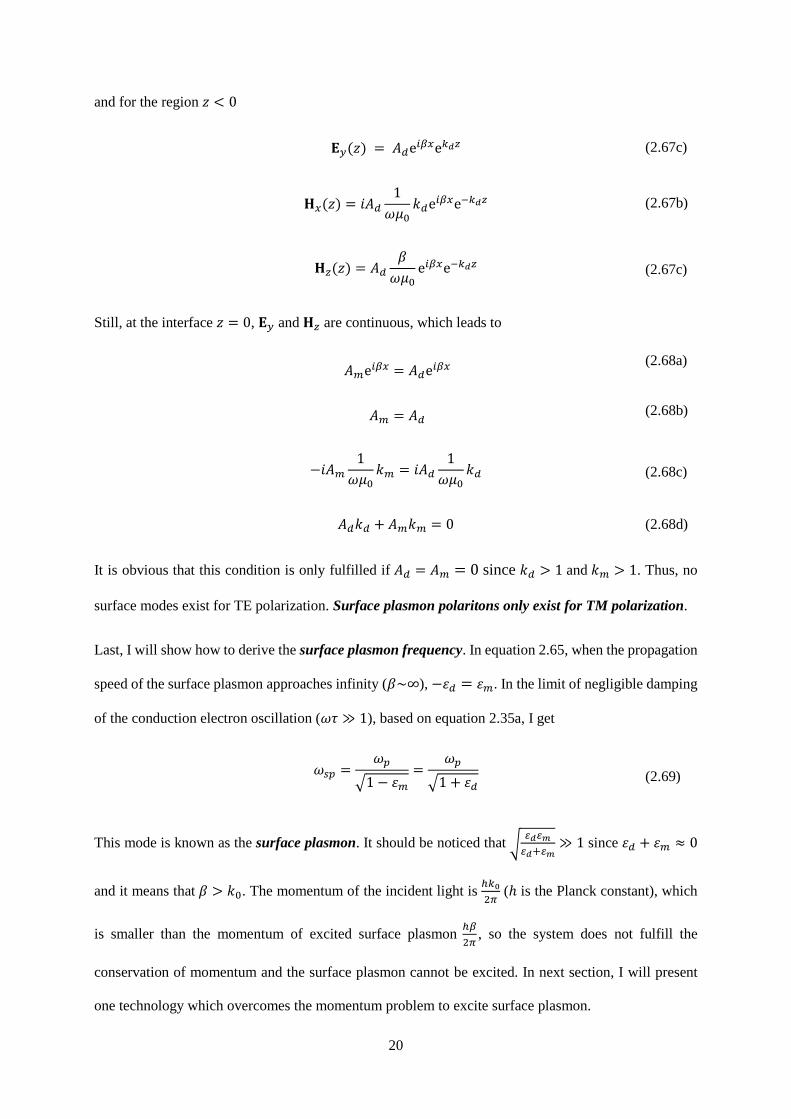
The Fig. 2.6 shows the extinction spectrum of different nanoholes samples. It is quite clear that the peak
positions of different diameters nanoholes are almost the same, which are around 650 nm [14]. However,
the dip positions have obvious blue shifts with decreasing diameters. In fact, the dip position is more
related with the localized surface plasmon resonance (LSPR) [15], which can mainly decide the
Figure 2.5. Plasmonic signal of nanoholes with 150 nm diameter, 320 nm periodicity and 30 nm thickness.
25
transmission of the incident light. Since LSPR is mainly decided by the hole sizes, the dip position varies
with the diameters of the holes.
The wavelength of a photon with strongest LSPR could be calculated by the function
Re{𝜀𝑑 + L[𝜀(λ𝐿𝑆𝑃𝑅) − 𝜀𝑑]} = 0
where 𝜀𝑑 is the refractive index of the environment and L is a geometrical constant. Equation 2.65 is
used to caculate the LSPR mode of nanodisks, L ∝ ℎ/𝐷, 𝐷 is the diameter of the nanodisks, ℎ is the
thickness. Then, ԑ (λ𝐿𝑆𝑃𝑅) ∝ ℎ/𝐷 since ԑ (λ𝐿𝑆𝑃𝑅) < 0 and λ𝐿𝑆𝑃𝑅 ∝ 𝐷/ℎ since ԑ(𝜆) = 1 −𝜔𝑝
2
2𝜋
𝜆
𝑐< 0
for visible light. So the dip position should have a redshift with increased diameter of the nanodisks.
Nanohole structure have similar properties as the nanodisk, however, it is also influenced by the
periodicity. I emphasize that a full understanding of the optical properties remains challenging and one
(2.65)
Figure 2.6. The spectrum of different nanoholes samples. The diameter changes from 130 nm to 70
nm. The periodicity is constant 320 nm and the gold thickness is 30 nm.
(2.65)
26
should not interpret the peak and dip as two independent spectral features. Based on my study and these
paper results [16] [17] [18], the dip position behaves like a localized resonance.
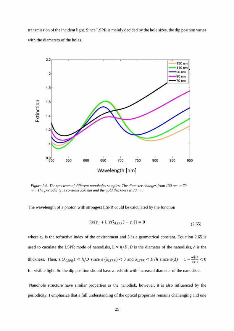
Besides the influence of the geometrical structure on the peak and the dip positions of the spectrum, the
refractive index of the environment can also affect them. For an environment with higher refractive
index, both the peak and the dip will red shift. Fig. 2.7 shows the relationship between the shifts and the
refractive index of the environment. Nanohole samples with two different diameters, 60 nm and 160 nm
are used. In this experiment, different water solutions with an increasing amount of glycerol (5, 10, 15,
20, 25, 30 and 35 percent by weight) are used to change the refractive index of the environment. With
higher concentration, the refractive index will increase and cause linear red shifts on the peak and the
dip positions. In Fig. 2.7B, it is quite clear that the amount of shifting for the peak and the dip is not
very related with the diameter of the nanoholes.
Figure 2.7. The relationship between the shifts and the refractive index of the environment.
27
Chapter 3 Plasmonic color generation
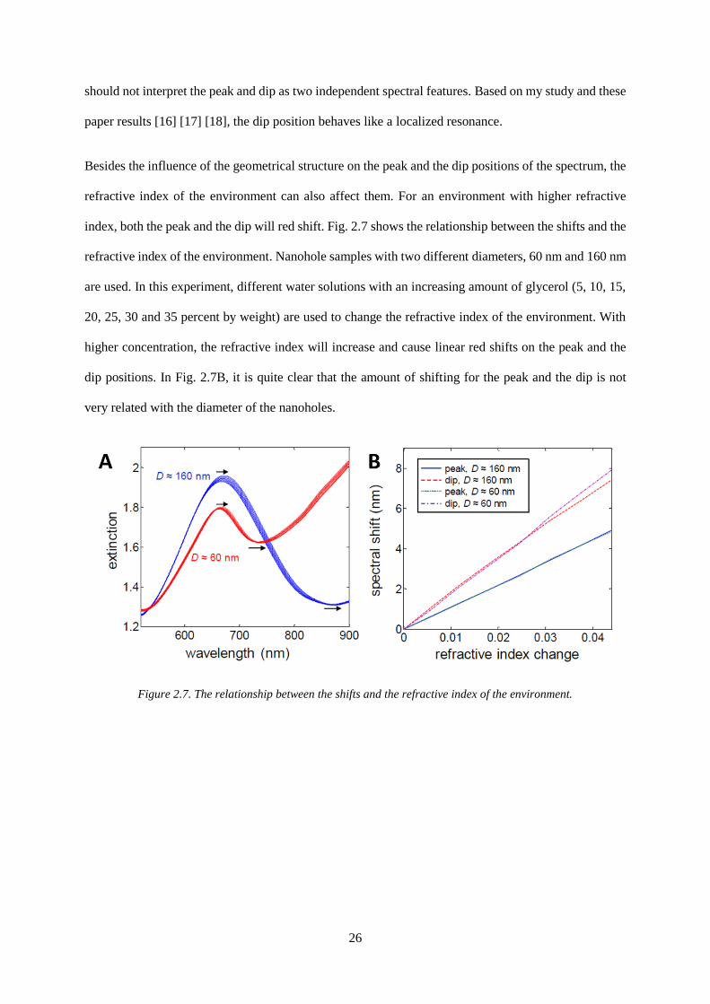
Stained glass had been used several thousand years ago for creating bright and permanent colors by
utilizing plasmons [19]. Chromatic glass contains tiny proportions of nanoparticles of metals or metallic
derivates scattering or absorbing visible light. One of the earliest and most known examples is the so
called Lycurgus cup (Figure 3.1a) which is a Roman glass cup made in the 4th century. One interesting
physical phenomenon is that the color of the cup changes from red to green depending on the direction
of the light source luminance. It shows red color when lit from behind and green when lit from in front.
This is because the stained glass of the Lycurgus cup has dichroic properties due to the surface plasmon
resonances of the metallic nanoparticles in the glass. The nanoparticles can absorb the blue light, scatter
the green light and transmit the red light.
Another widely used application for stained glasses is colored patterning the windows of churches
(Figure 3.1b) [20], mosques and other significant buildings. In medieval Europe, the patterned windows
Figure 3.1. (a) The cup in reflected (left) and transmitted light (right) (b) The north transept rose of Chartres
Cathedral is comprised by stained glass. The image is from reference [19].

28
made by stained glasses instead of painting pictures directly on the windows due to the lifetime of the
colors of the stain glasses, which last as long as the glass itself. For getting strong colors different kinds
of materials and sizes of the nanoparticles are used in the glass. The whiteness can also be adjusted by
the concentration of the colloidal particles. Not only the metallic particles but also metallic derivates are
used for creating colors. For instance, Iron (II) oxide can be used for green color and copper oxide
produces turquoise color. The church windows are patterned by assembling lots of small pieces of
chromatic stained glass on a rigid frame. By using this technology, the pictures made of stain glasses
keep the brilliant colors even until now.
In the next sections, we will introduce different color generation technologies by using “modern
plasmonic”. With the development of nanotechnology, different metallic nanostructures can be
accurately fabricated and the scattering, reflection and transmission of the nanostructures can thereby
be tuned in the visible light range [21]. In section 3.1 and 3.2, the basic theories and models are discussed
and several representative structures are presented and analyzed.
3.1 Structural color from plasmonic nanodisk and metallic grating
As a 2D (one metallic layer) plasmonic material, nanodisks can be accurately fabricated by electron-
beam lithography (EBL), focused ion beam (FIB) [22] and Hole-Mask colloidal lithography (HCL) [23].
The precise size-controlled plasmonic nanodisk can be used to scatter a specific visible wavelength just
like a color filter [24]. By changing the geometry and size of the nanodisk, the scattered wavelength can
be adjusted since it changes the dipole moment and localized surface plasmon resonances (LSPR) of the
nanodisk [25]. With the geometry adjustment, the optical spectrum of the plasmonic nanodisk is
different in different metals. Silver and aluminum are normally used for display purposes since their
interband transitions are mainly in the UV region [26] [27]. The scattering spectra of aluminum
nanodisks fabricated on UV-grade fused silica substrates is shown in Fig. 3.2, which is published by N.J.
Halas group in reference [28]. As the diameter of the nanodisks increases (Fig. 3.2b), phase delay across

29
the nanodisk causes a redshift of the plasmon resonance (Fig. 3.2a). The scattering spectra of the Al
nanodisks is also calculated by the finite difference time domain (FDTD) method (Fig. 3.2c). Even
though the nanodisks have some small geometrical defects, the experimental results do not have
significant deviations from the simulation. To achieve the full visible colors scattering, the diameter of
the Al nanodisk need to be accurately adjusted from 90 nm (purple) to 180 nm (red) with constant
thickness ~ 35 nm. Comparing with conventional chemical pigments, the plasmonic Al nanodisks have
much stronger interaction with light, which provide a novel display technology with ultra-high
resolutions and an ultra-thin system.
Figure 3.2. (a) Experimental dark-field spectra of individual nanodisks with D = 70, 80, 100, 120, 130, 150,
180 nm. (b) SEM micrographs of the corresponding nanodisk structures. Scale bar is 100 nm. (c) FDTD
simulations of the nanodisk spectra, assuming a 3 nm surface oxide and a SiO2 substrate. The image is from
reference [28].

30
Another 2D plasmonic nanostructure is grating-based nanorod array [29], which utilizes the diffraction
phenomena to choose specific wavelengths of light to be transmitted or reflected from the material.
Figure 3.3 shows how the plasmonic grating works. The incident light scatters from the periodic
structure and excites LSPR modes on the silver nanowires. LSPR modes lead a phase delay which can
interfere with the incident light thus influence the reflection and transmission. Since the optical signal
is very sensitive to the periodicities of the grids, the grating structure is normally fabricated by EBL for
its high accuracy [30].
Comparing with the nanodisk-based structure, one big difference is that the reflection and transmission
of the grating-based displays is polarization dependent. LSPR can only be excited by the polarized light
oscillating perpendicular to the grid direction, which means it can only work for 50% of the natural light
since it contains both S (perpendicular) and P (parallel) polarizations.
Figure 3.3. normal incident light containing TE and TM modes passes through the silver grid nanostructure,
only TM mode can excite LSPR and lead to a phase delay.

31
Normally, grating-based nanostructure needs to work with polarizers for displays since the polarizer can
filter out the incident light with the correct polarization. One of the most used materials is liquid crystals
which are birefringent and can be modulated by applying voltages. Figure 3.4 shows how the transmitted
colors change with different polarization of incident light, the image is published by L. Novotny group
in reference [31]. In Figure 3.4, the transmission image is from grating-based silver grids with seven
different thicknesses printed in different regions. The dimensions of the grids decide the LSPR mode
which shows a strong resonance at a specific wavelength. Meanwhile, the colors can also be modulated
by changing the polarization angle.
3.2 Color generation from multilayer nanostructures
Comparing with a single layer plasmonic color generator, multilayer plasmonic nanostructures provides
better quality colors and are normally used for reflection or scattering. Plasmonic nanodisks can be
Figure 3.4. The image consists of silver grids with different thickness which generate different colors in
different regions. The image is from reference [31].

32
combined with a back-reflector to enhance the reflected color since this reflects the forward scattered
light (Figure 3.5). Based on the multilayer nanodisk structure, color images can be printed with an extra
high resolution which is ~100000 dots per inch [32]. The resolution of the traditional color printing
based on ink deposition is limited by the size of each ink spot. Normally, the ink-spot sizes are around
25 𝜇𝑚 which means the resolution is lower than 1000 DPI and it is already achieved in commercial laser
printers. In figure 3.5, the diameter of the nanodisk is only around 100 nm which is the limit of the
minimum size of the plasmonic pixels, thus the plasmonic images can reach an ultra high-resolution. To
fabricate the multilayer plasmonic images, EBL which provides accurate size control is normally used
since the colors of this structure are very sensitive to the diameter of the nanodisks.
Recently, Anders Kristensen group tried to use a single-pulse laser to reshape the nanodisks to tailor the
colors [33]. First, they printed multilayer nanodisks with the same size on a substrate, then a laser pulse
of nanosecond duration is used to melt the nanodisks. Since the melting changes the morphology of the
nanodisks, which shifts the resonant frequency of the LSPR, different colors can be generated. By
controlling the parameters (power, spot size, etc) and the position of the laser pulse, different sizes of
nanodisks can be patterned in different regions of the metasurface. Figure 3.6 shows how the system
works and the image made by this technology.
Figure 3.5. Multilayer plasmonic nanostructure is comprised by a back-reflector, HSQ (dielectric) and
nanodisks. By changing the size of the nanodisks, different colors can be reflected back. The image is formed
by printing different sizes of nanodisks in different regions. The image is from reference [32].

33
Normally, the multilayer nanodisk structure needs a highly accurate fabrication technology since the
colors are very sensitive to the geometry of the nanodisk. Thus, it is a big challenge to pattern these
structures over a large area (like centimeter level). In this work we propose a novel multilayer nanohole
structure to generate colors, which can be efficiently fabricated over tens of centimeters. The structure
is shown in Figure 3.7.
Figure 3.6. a) A schematic illustration of laser printing. b) Printed images in different color schemes. Scale
bars: 5µm. The image is from reference [33]
Figure 3.7. a) A schematic of the metasurface. b) A photo of samples with the primary colors under ambient
light. c) A photo of a sample on polyethylene terephthalate (PET) support with a color palette generated by a
gradient in alumina thickness. The middle region has no nanoholes in the gold film. d) Reflection spectra in
air of the red, green, and blue samples for different angles.

34
Our metasurface also consists of three layers (Figure 3.7a). First, a silver reflector was deposited on the
substrate and the subsequent alumina spacer layer is designed to tune the reflective color by Fabry-Pérot
interference. Next, short-range ordered nanoholes in a gold film were prepared on alumina by colloidal
lithography and tape stripping. Comparing with EBL or FBI, colloidal lithography consists of parallel
processing steps compatible with large areas and plastic supports, which made the material flexible (Fig.
3.7c). More details about the colloidal lithography will be discussed in following sections. A color
palette is fabricated by varying the alumina thickness and the high resonant reflectivity (~90%) (Fig.
3.7d) confirmed the clear colors of the nanomaterial (Fig. 3.7b).
Since the nanohole array structure can be fabricated over a large area and has a very high reflectivity, it
can directly use the traditional RGB pixel triplets to generates chromatic images. RGB pixel triplets
have been mentioned in the introduction part as the most common technology for all the commercialized
displays. They can provide the largest color gamut by tuning the intensity of each pixel. For generating
RGB colors, only utilizing the Fabry-Pérot interference between the top and bottom metallic layers is
not enough. We need to fabricate the short-range ordered nanoholes to scatter away the redundant visible
light. Figure 3.8 shows both the bright and dark fields of these RGB pixel triplets. By dark-filed
illumination, we verified that the three RGB structures with nanoholes scattered their complementary
colors at high angles. In order to show that the RGB pixel triplets can generate secondary colors, we
produced microscale pixels of red, green and blue and patterned them in different regions.
Figure 3.8. The bright field and dark field of the RGB pixel triplets.

35
Figure 3.9 shows how the secondary colors yellow, purple and cyan can be produced by their
RGB combinations and a sample with RGB pixels patterned to display the University logo in
different colors. For the above figures 3.7 to 3.9, the short-range ordered nanoholes are
fabricated on the gold surface. In fact, the gold layer can be replaced by a copper layer. The
price of copper is several thousand times lower than gold and the red color from the copper
multilayer nanohole structure is better than the gold. Figure 3.10 shows the image of Lena
formed by the copper based plasmonic pixels. The pixel size of each primary color is around
Figure 3.9. a) The secondary colors are generated. b) A sample with RGB pixels patterned to display the
university logo in different colors.
a) b)
Figure 3.10. a) The image “Lena” made by the copper plasmonic RGB pixels. b) The standard Lenna image
which is widely used to test the quality of colors in the field of image processing.

36
30µm*100 µm, which is smaller than the resolving power of human eyes. Because of the high
reflectivity of each pixel, the image shows colors which are close to a real commercial display.

37
4. Nanofabrication of plasmonic materials
In the previous chapter, we roughly described several widely used nanofabrication technologies. Here,
we will introduce more details about these technologies. Electron beam lithography (EBL) is one of the
most widely used technologies for nanofabrication. It can reach extra high accuracy (~10 nm) [33].
However, EBL can only work for small samples since it is limited by the writing speed. Colloidal
lithography (CL) is a nanofabrication technology which can be used for large area fabrication. This
chapter will discuss both good and bad sides of these two technologies. Since we focus more on the
large area fabrication technology, more information about CL will be presented.
4.1 Electron beam lithography (EBL)
The process of EBL is quite similar with laserlithography, the difference is EBL using the electron beam
instead of the light beam [34]. First, the electron-sensitive resist needs to be coated on a substrate. Two
different kinds of resists can be selected. One is positive resist which means the resist becomes
dissolvable in the developer after exposing, another is negative resist which becomes hard to dissolve
in the developer after exposing. The resist normally is coated by a spinner and the thickness of the resist
can be adjusted by the spinning speed.
Second, the resist should be heated to change from the liquid state to the solid state. Depending on the
kind of resist, different temperatures are required and also different heating times. Third, the substrate
coated by resist is placed in a vacuum chamber and the electron beam is used with proper parameters to
write the pattern on the substrate. Fourth, the sample is put into resist developer to remove the exposed
part for positive resist or unexposed part for negative resist. A substrate with remaining resist pattern is
achieved and will be used as a mask.

38
Then, metals and dielectrics are deposited on the patterned substrate. After removing the sample from
the chamber, a resist remover is used to dissolve the remaining resist which is covered by the metals or
dielectrics now. Then only the metals or dielectrics which are directly deposited on the substrate remain
and form the plasmonic nanomaterial. Normally, the minimum size of the nanostructure is decided by
the size of the electron beam, which can reach ~10 nm under perfect conditions [35]. In comparison
with the colloidal lithography (CL), EBL can precisely pattern the plasmonic structure which is
especially important to easily change the periodicity. However, the slow writing speed limits its use for
large area patterning and EBL also needs to work in a vacuum environment which increases the cost
and processing time a lot.
4.2 Colloidal lithography (CL)
Colloidal lithography (CL) is much cheaper and faster than EBL and utilizes nanoparticles as a mask
instead of the electron beam processed resist [36]. After depositing metals or dielectrics and removing
the nanoparticles, each nanoparticle can form one nanohole which is almost the same size as the
nanoparticle. Because the nanoparticle mask can be made in a few minutes, it saves lots of time in
comparison with EBL. In addition, CL doesn’t need a special machine to provide vacuum environment
which saves lots of money as well. However, CL is limited by the structure of the nanoparticles, which
can not be used for fabricating complex nanostructures. The periodicity of the nanoparticles is hard to
precisely control compared with EBL [37]. We use the multilayer nanohole structure to generate colors
for displays and it is made by CL. In this section, we will present more details of this technology.
The short range arrayed nanoholes in a gold film is one of the simplest structures prepared by colloidal
lithography (CL). Both the size and periodicity of nanoholes can be roughly adjusted by using different
colloidal solutions. Figure 4.1 shows the basic steps of fabrication of nanohole samples. The first step
is adsorption of plastic particles on the glass substrate. Because the plastic particles have negative
charges, the glass substrate needs positive charges to attract the particles. The positive charges can be

39
introduced by putting the aluminum chlorohydrate (ACH) on the surface. The 5% concentration ACH
solution should be dropped on a glass substrate first and left around 1 minute. Then, the sample should
be rinsed and dried by nitrogen gas. Later, the colloidal solution is drop coated on the substrate followed
by waiting another 2 minutes for the particle adsorption. To reinforce the stability of the plastic
nanoparticles on the substrate, boiled ethylene glycol can be drenched on the substrate. The second step
is deposition of different materials. 1 nm Cr should be deposited first because it is the adhesive layer
between the glass substrate and the gold layer. Cr layer helps gold strongly attach on the glass substrate.
Then, gold layer tens of nanometers in thickness is deposited and the deposition speed should be around
1 Å/sec. The last layer is 15 nm Al2O3 which is used to protect the gold surface for step 3. In step 3, the
colloidal particles should be removed by a soft material like rubber or sponge. The Al2O3 layer protects
the gold surface from being scratched by the soft material. After removing the particles, the last step is
removing the Al2O3 layer. The Al2O3 layer can be removed in 30 mM NaOH solution. The standard way
is to put the samples into the NaOH solution and wait around 1 hour. After drying, the nanoholes are
formed.
For the nanoholes structure, both the size and periodicity of nanoholes are totally decided by the particles
in the colloidal solution. Particles with different sizes can be bought directly from a company. The
distance between the neighboring particles is dependent on the amount of charges on the particles. In
general, the smaller particles have less charges, so the distance between small particles is shorter than
between large particles.
Figure 4.1. The process of colloidal lithography for short-range ordered nanoholes.

40
For size adjustment, different sizes of particles can be used to fabricate different nanoholes. However,
one disadvantage of this method is that the size uniformity of particles is not good when the particle size
is below 100 nm. Figure 4.2 shows different sizes of nanoholes which are made by colloidal lithography.
It is quite clear that for the 58 nm nanoholes (top left), the size uniformity is quite bad. In fact, lots of
nanoholes are larger than 60 nm and we estimated that the average size of nanoholes is 65 nm, not 58
nm as specified. Using quite small nanoparticles to get quite small nanoholes seems not to be an effective
way. However, with increasing size of particles, the uniformity looks much better. The nanoholes with
105 nm diameter (bottom right) have much less size variation than 58 nm nanoholes.
Recently, one new method which can be used to fabricate uniform small nanoholes was invented [35].
It conserves the uniformity of large nanoholes and produces quite small nanoholes which are around 50
200 nm
58 nm 67 nm
80 nm 105 nm
Figure 4.2. Different sizes nanoholes were made by different colloidal solutions.
Figure 4.3. The process of shrinking the nanoparticles to get smaller nanoparticles.

41
nm. The method is that of shrinking the big particles by oxygen plasma after the particles are adsorbed
on the substrate. After oxygen plasma shrinking, the size of particles becomes much smaller. Because
the shrinking rate is quite uniform for each particle and the large particles have relatively uniform size,
the shrunk small particles are also quite uniform [35].
The size of shrunken particles can be adjusted by the shrinking time. The average shrinking speed is
around 1 nm/s. Fig. 4.3 shows the shrinking process. The initial size of particles is 158 nm. After the
particles are absorbed on a substrate, they can be shrunk by oxygen plasma. The plasma power is 50 W,
the pressure is 250 mTorr and gas speed is 80 sccm. Since the initial size of colloidal particles is 158
nm and the average shrinking speed is 1 nm/s, the shrinking time is around 108 s. One important point
of using the oxygen plasma shrinking is that the shrinking speed could be not very stable because the
shrinking speed is also related to the surface temperature of nanoparticles and the temperature of the
nanoparticles will increase during the shrinking process [38]. To get more stable shrinking speed, the
best option is cooling the sample after every 10 sec shrinking.
Figure 4.4 shows the nanoholes under SEM. It is obvious that these samples have almost the same
uniformity. To compare with the samples directly made by small particles, the diameters of all the
Figure 4.4. The SEM image includes four different nanoholes samples made by the same colloidal solution.

42
samples are analyzed. Fig. 4.5 shows the measured diameter histograms. For the samples which are
made by particle shrinking, above 90% of nanoholes are in a variation of ±4 nm even for 50 nm
nanoholes. However, for the nanoholes which are directly made by 58 nm particles, the size variation
of the nanoholes is much larger.
Figure 4.5. The histograms of measured diameters. The left figure is achieved by using the shrinking technology to
get nanoholes. The right figure is achieved by directly using different sizes of PS particles to get nanoholes.

43
5. Implementing electrochromic polymers
In this thesis, I present a novel plasmonic electronic paper technology. The electronic paper includes
two main parts where one is the color generator which has been described in Chapter 3. The other part
is the color modulator which is made of electrochromic conjugated polymers (ECPs). I have already
presented that the multilayer nanohole structure provides a high reflectivity and the thickness of the
whole structure is only around hundreds of nanometers. I also presented that images made by plasmonic
nanomaterials can have an extra high resolution. However, if I want to make a display based on the
plasmonic nanostructures, I need to figure out a modulator which also has a thickness similar to the
plasmonic materials. The reason is that the thickness of the modulator can limit the viewing angle of the
display. Since the thickness of the liquid crystals is on the millimeter level which is much larger than
the pixel size (hundred micrometers) [39], a small change in viewing angle can lead to a misalignment
between the liquid crystal and the pixel. Thus, an electrochromic conjugated polymer is one good
candidate since it can modulate the optical signal with hundreds of nanometers thickness and its soft
texture perfectly matches with the plasmonic nanomaterials for a bendable display. In addition, the
optical properties of the polymer can be maintained without applying voltages, which means it does not
need energy to display static images [40]. Comparing with LCD and LED which need constant voltages
when displaying, plasmonic electronic paper significantly reduces the energy consumption [41]. This
chapter will first introduce the basic theory of the conjugated polymer and review several different kinds
of electrochromic polymers. Then it will introduce the technology combining plasmonic materials and
polymers. Last, I will discuss the optical properties of the novel plasmonic electronic paper.
5.1 Introduction of electrochromic conjugated polymers
Electrochromic polymers are characterized by a change in their optical properties upon reduction or
oxidation, which is controlled by an electrical voltage. After discovering and characterizing the

44
polyacetylene [53], the study of conjugated polymers rose rapidly. There are a lot of applications for
conjugated polymer i.e. solar cells, organic light emitting device (OLEDs) and electrochromic devices.
Normally, the conjugated polymer is p-type electroactive compounds since positive charges are
generated upon oxidation. The positive charges of conjugated polymers can migrate along the chain by
delocalized electrons in the alternating double bonds of the chain. These currents are responsible for the
conductivity of the polymer [43], Fig. 5.1 shows how the system works. During the oxidation, the
polymer has a local distortion of the chain in the proximity of the charge, then it is pictured as a quinoid-
like structure in which single bonds assume double bonding character [44].
To further analyze the physical model of the conjugated polymer, I introduce the band diagrams to
explain the optical properties. Depending on the doping levels, the conjugated polymers have polaron
states (low doping) or bipolaronic states (high doping) respectively. In conjugated polymers with a
ground state (Fig. 5.2a), the positively charged states are called bipolaron states, which are localized
inside the band gap of the polymer (Fig. 5.2b) [45]. For the bipolaronic state polymer, there are two sub-
gap (low energy) transitions from the valence band to the localized (𝐸𝑏1 and 𝐸𝑏2) bipolaronic states.
Figure 5.1. The process of oxidation of a conjugated polymer.
Figure 5.2. The neutral and bipolaron states of the conjugated polymer.
𝐸𝑔
𝐸𝑏2
𝐸𝑏1
CB CB
𝐸𝑔
Bipolaron
states

45
The optical absorption band in the reduced neutral conjugated polymer is determined by a 𝜋 − 𝜋∗
transition through the band gap [46]. Thus, the energy levels of the localized bipolarons dominate the
optical properties since the observed color depends upon the bandgap of the polymer. Thin films of
polymers with 𝐸𝑔 > 3 eV are colorless since it is out of the visible color range. However, they can
become colorful if their doped forms absorb visible light. In contrast, those with lower band gaps 𝐸𝑔 <
1.5 eV show colored reduced forms and have a weak colored or colorless doped form. After the doping,
the absorption shifts to the NIR region which cannot be seen by human eyes. In next section, I will
review several electrochromic conjugated polymers, such as PEDOT. PEDOT has “bright state” in its
oxidized state and polypyrrole (ppy) has “black state” in its oxidized state [47] [48]. I will also discuss
their optical properties.
5.11 Poly [3, 4-(ethylenedioxy) thiophene] (PEDOT)
PEDOT possesses a relatively stable and highly transmissive sky-blue oxidized state, which is suitable
for a polymer-based electrochromic device (ECD) [49]. The absorption band of reduced PEDOT lies in
the near infrared region which leads to a dark blue color. PEDOT has a fairly high optical contrast, good
mechanical properties, low switching times and low cost [50]. Meanwhile, PEDOT is a good electrical
conductor which keeps its conductivity in both reduced and oxidized states [51]. This property is hard
to find in other conjugated polymers. In our devices, I use PEDOT to modulate the optical properties of
the copper-based plasmonic samples, as will be discussed later.
Figure 5.3. The chemical reaction of polymerization of the EDOT monomer.
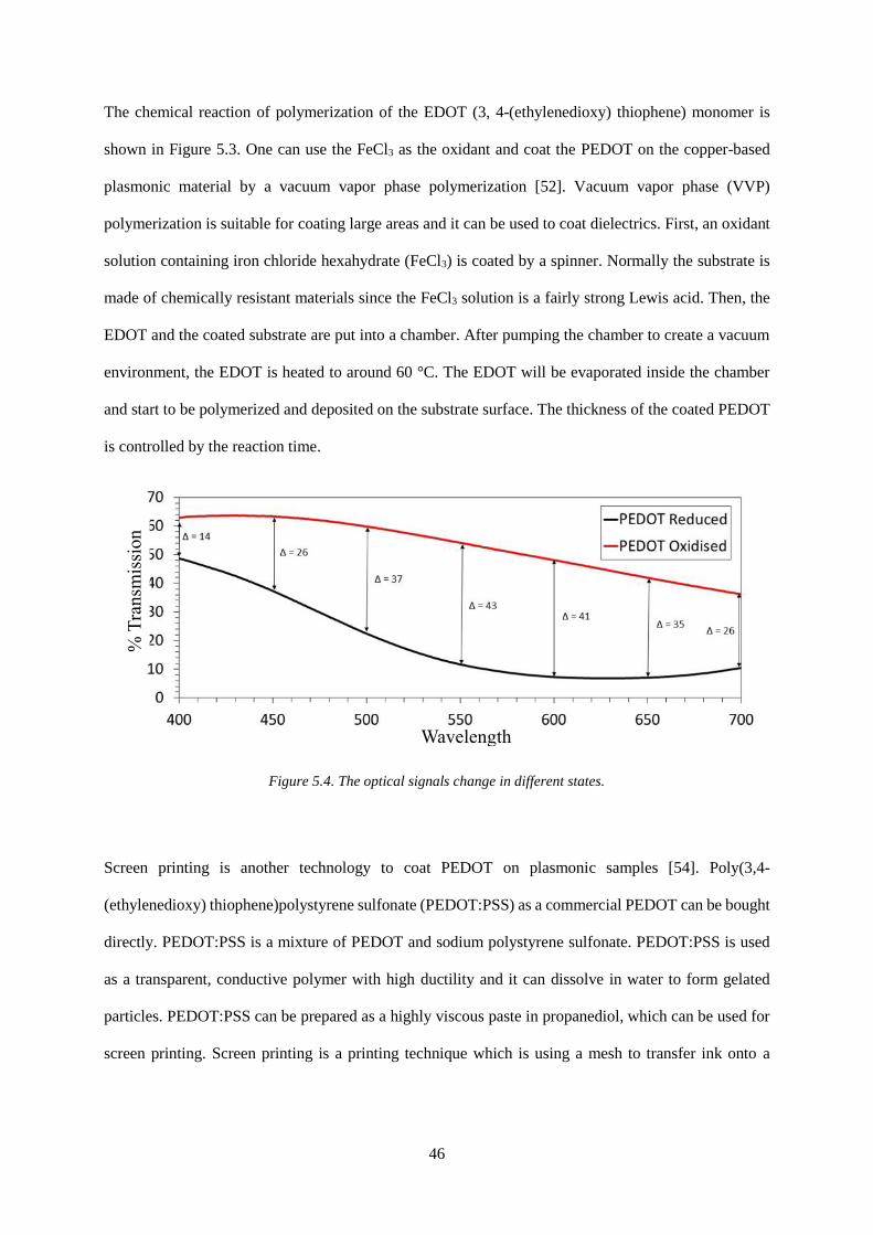
46
The chemical reaction of polymerization of the EDOT (3, 4-(ethylenedioxy) thiophene) monomer is
shown in Figure 5.3. One can use the FeCl3 as the oxidant and coat the PEDOT on the copper-based
plasmonic material by a vacuum vapor phase polymerization [52]. Vacuum vapor phase (VVP)
polymerization is suitable for coating large areas and it can be used to coat dielectrics. First, an oxidant
solution containing iron chloride hexahydrate (FeCl3) is coated by a spinner. Normally the substrate is
made of chemically resistant materials since the FeCl3 solution is a fairly strong Lewis acid. Then, the
EDOT and the coated substrate are put into a chamber. After pumping the chamber to create a vacuum
environment, the EDOT is heated to around 60 °C. The EDOT will be evaporated inside the chamber
and start to be polymerized and deposited on the substrate surface. The thickness of the coated PEDOT
is controlled by the reaction time.
Screen printing is another technology to coat PEDOT on plasmonic samples [54]. Poly(3,4-
(ethylenedioxy) thiophene)polystyrene sulfonate (PEDOT:PSS) as a commercial PEDOT can be bought
directly. PEDOT:PSS is a mixture of PEDOT and sodium polystyrene sulfonate. PEDOT:PSS is used
as a transparent, conductive polymer with high ductility and it can dissolve in water to form gelated
particles. PEDOT:PSS can be prepared as a highly viscous paste in propanediol, which can be used for
screen printing. Screen printing is a printing technique which is using a mesh to transfer ink onto a
Figure 5.4. The optical signals change in different states.
Wavelength
% T
ran
smis
sio
n

47
substrate. In my case, the thickness of PEDOT:PSS can be adjusted by the thickness of the mesh or the
polymer concentration in the solution.
Concerning the optical properties of the PEDOT, Figure 5.4 shows the visible spectrum of PEDOT in
different states. It is obvious the PEDOT has relatively high optical contrast (~40%) for the green
(520nm to 560nm) and red color (620nm to 740nm). However, because of the contrast in blue (450nm
to 490nm) is less than red and green, it is hard to get a completely black state and some blue color
remains. Even though I can adjust the contrast by depositing PEDOT with different thicknesses for
modulating different colors, precisely controlling different thicknesses in different areas of one substrate
is still a big challenge for both VVP and screen printing technologies, which is important for electronic
paper application. More details about modulation of PEDOT-plasmonic materials will be discussed later.
In the next section, I will discuss another kind of conjugated polymer which is polypyrrole (ppy).
5.12 Polypyrrole (PPy)
Polypyrrole (PPy) is by far the most extensively studied polymer in this research area because of its low
oxidation potential, water solubility and the low cost of its monomer [55]. PPy is in black or bright
modes for the oxidized or reduced states respectively, which is the opposite of PEDOT. Thus, PPy and
PEDOT could be used as the cathode and anode sides in an electrochemistry system to modulate the
optical signals. For the synthesis of PPy, electrochemical polymerization is a frequently used technology
because it requires a small amount of monomer and it provides an effective platform that allows
investigating the growing process of the polymer by electrochemistry and spectroscopy [56]. Figure 5.5
shows a system that contains combined electrochemical and spectroscopic systems. The system uses
Ag/AgCl as the reference and Pt as the counter electrode which is connected to the potentiostat to control
the voltage and measure the current. Meanwhile, the light source is coupled to an optical fiber and the
spectrum can be measured by a fiber-coupled spectrometer. Since copper is an easily oxidized metal it
will be etched during electrochemical deposition and thus I have to use the gold containing color

48
generators. The solution for deposition is a mixture of NaDBS and pyrrole. Before electrochemical
deposition, I install the gold color generator in a flow cell which contains the reference (Pt) and
counter(Ag/AgCl), then inject the mixture. The polypyrrole will be deposited by applying +0.57 V
versus Ag/AgCl and the growth rate is around 40 nm/min. This process is monitored by the plasmonic
sensing with high resolution [57] and the thickness can be accurately controlled by the current.
The mechanism of polymerization of pyrrole is shown in Fig. 5.6. The oxidized monomers bond together
to form a long chain. It should be noticed that DBS is also doped into PPy during the electrochemical
deposition. In fact, PPy does not consist of linear chains but is heavily crosslinked [58] (Fig. 5.6). This
crosslink traps the DBS within the PPy matrix. For the optical properties, PPy has an even weaker
contrast for blue color. The optical property of the polymerized sample is modulated by electrochemistry
[59]. One only needs to exchange the solution from the mixture with pyrrole to only NaDBS. About the
optical property modulation, it will be discussed in the next section.
5.2 Electrochemical modulation
For both PEDOT and PPy based plasmonic electronic papers, electrochemical technology is used to
modulate the reflection. The color is easily switched “on” or “off” by applying maximum ±1 V. The
Figure 5.6. Polymerizing pyrrole to form PPy. The image is from reference [58].

49
whole system can be flexible if a soft substrate (plastic) and a suitable counter/reference (thin ITO,
polymer, carbon paste, etc.) are used [60]. Fig 5.7 shows a system consisting of PPy and gold based
plasmonic color generators, and the reflection is electrochemically controlled. Since gold is one of the
best conductors and it has a strong chemical resistance, a thin (~20 nm) gold layer can work as the top
layer of the color generator and also as a working electrode which controls the “on” or “off” state of the
PPy. Then color is switched “on” by applying around ~-1 V (vs Ag/AgCl) to reduce the conductive
polymer to its neutral state, leading to strongly reduced absorption [61]. As a result, the reflections from
the RGB samples can be modulated with a high contrast.
The spectra of RGB samples in “on” or “off” state and the sensitive region of the human eye under well-
lit conditions are shown in Figure 5.8. The reflections from the RGB samples could be modulated with
high contrast. The spectra are slightly shifted compared with the initial colors since the structures now
are in contact with polymer and electrolyte, but the colors appear very similar. The sensitive region is
defined as the wavelength interval where the luminosity function for photopic vision is > 5% of its
maximum.
Figure 5.7. Electrochemical control of “on” and “off” states of color generators.

50
Comparing with gold-PPy, PEDOT-copper based plasmonic electronic paper is much cheaper with
better optical contrast, especially for blue color. Since copper is not as chemically stable as gold, it can
not be directly used as a working electrode. Thus, I cannot use electrochemical technology to deposit
PPy on copper. One needs to coat a protection layer on the copper surface to avoid etching due to the
electrolyte solution. In our case, I first deposit 20 nm Al2O3 after the colloidal lithography and then an
Figure 5.8. Reflection spectra and images of RGB samples in on/off states.
Figure 5.9. a) Pictures showing “on” and “off” states of RGB samples. b) The whole system is bendable.
c) Reflection spectra of RGB samples in “on” or “off” state.

51
additional 100 nm SiO2 to cover the nanoholes and defects of the Al2O3 layer. PEDOT is perfectly
matched with the copper-based plasmonic samples. It can be used as a working electrode since it is a
conductor in both reduced and oxidized states and it also works as an optical modulator. I print PEDOT
on the plasmonic color generator by screen printing and the “on” and “off” states for RGB samples is
shown in Fig. 5.9. In this system, I use thin ITO (25 nm) as the counter and PET as the substrate, so the
whole system is bendable (Fig. 5.9b).
In conclusion, these reflective color displays should be especially useful for large-area energy-efficient
electronic readers and posters, which are also simple to fold and transport. For the PEDOT- copper based
electronic paper, the cost of the materials is low and commercially available. More details about the
plasmonic electronic paper will be discussed in the next chapter.

52

53
6. Discussion and future outlook
In this chapter, more details about the plasmonic electronic paper will be discussed, which
include the color analysis, energy consumption and response time. We compare the properties
of plasmonic electronic paper with other similar devices and also discuss the merits and
drawbacks. Last, the future outlook of electronic paper is presented. We will briefly introduce
some future plans to improve our devices.
6.1 Discussion on plasmonic electronic paper
First, we introduce some background about the characterization of color from displays. The CIE color
space is used to define the quantitative links between physically measured wavelengths and
physiologically perceived colors in human eyes [62]. The human eyes have three kinds of cone cells to
sense colors, which are sensitive in 420-440 nm as the short wavelength region, 530-540 nm as the
middle wavelength region and 560-580 nm as the long wavelength region. Based on the three regions,
people set up a CIE XYZ color space encompassing all color sensations that an average person can
Fig. 6.1 Chromatic calculation for the RGB copper based on the plasmonic metasurface.

54
experience. CIE color space is used as a standard reference to estimate the quality of color generators
and the occupied area of the CIE color space represents the color gamut. Fig. 6.1 shows the color gamut
of the copper-based plasmonic color generators. All colors inside of the triangle can be generated by
mixing three primary colors represented by the points in the chromaticity diagram. The color range of
the RGB metasurfaces are according to the CIE “standard observer” functions from 1931 [62]. The
CIE’s color matching functions x(𝜆), y(𝜆) and z(𝜆) denotes the chromatic response of the observer. We
first calculate the tristimulus values based on the color functions:
𝒀 = ∫ 𝑹(λ)𝑦(λ)𝑑λ
780
380
𝒀 = ∫ 𝑹(λ)𝑦(λ)𝑑λ
780
380
𝒁 = ∫ 𝑹(λ)𝑧(λ)𝑑λ
780
380
where R is the reflectivity of the RGB samples and the integral range 380 to 780 nm represents the whole
visible region in nm. After normalizing, the CIE coordinates become:
𝒙 =𝑿
𝑿 + 𝒀+ 𝒁
𝒚 =𝒀
𝑿 + 𝒀+ 𝒁
𝒛 =𝒁
𝑿 + 𝒀 + 𝒁
For the copper based color generator, the coordinate of R is (0.52,0.33), G is (0.28,0.38) and B is
(0.19,0.15).
Second, I present the energy consumption of the plasmonic electronic paper. Similar to the EPD displays,
plasmonic electronic paper does not need to keep on supplying voltages or currents to maintain the
colors for the display under the right circumstances. Further, the voltages for switching the color are
(5.11a)
(5.11b)
(5.11c)
(5.12a)
(5.12b)
(5.12c)

55
much lower than EPD [63], which leads to much lower energy consumption. Considering the stability
of the electrochemical system, the ideal voltages of PPy for switching the colors fully on were -0.9, -
1.0. and -0.8 V vs Ag/AgCl for RGB respectively. We compare the energy consumption to emissive
displays (LED) and EPD, as is shown in Fig. 6.2. The power densities correspond the energy cosumption
of displays, and our plasmonic electronic paper is more than two orders of magnitude lower than LED
and one order lower than EPD [2].
Last, about the response time, the electronic paper takes less than 1 s to turn the colors on or off. In the
future it can be used to display images or texts but can not display videos. In Fig. 6.3a, the current trace
shows switching the metasurfaces every ~10 s and also the reflection variation together with the current.
The thickness of the PPy is around 200 nm. It is obvious that the reflection is stable after ~1 s which is
Fig. 6.2 The power density of the PPy-gold based plasmonic electronic paper for the RGB colors compared
with average power use for black and white electrophoretic displays and active-matrix organic light-emitting
diode (AM-OLED) displays.
Fig. 6.3 a) Switching dynamics (for a red sample) showing current (electrode area 176 mm2) and reflectivity
at 660 nm versus time as the voltage is reversed. b) Response times versus colors and PPy thickness.

56
shorter than the stable time of the electric current. More details about the shifting time for different RGB
colors and thickness of the polymer are shown in Fig 6.3b.
6.2 Future outlook
In this thesis, I have presented a novel electronic paper consisting of electrochromic polymers and
plasmonic color generators. I started with introducing the commercial displays like CCRT, LCD, LED,
etc. and discussed their limitations and merits. Then, the theoretic part of plasmonics is presented in
chapter 2, which provides the basic knowledge to understand the optical properties of plasmonic
materials. In chapter 3, several plasmonic color generators are discussed including their structure, size
and the elements used. My color generators which have metal-insulator-metal structures are discussed
later. After analyzing the optical properties of my color generators, the fabrication technologies are
presented in chapter 4 and I also discuss how to adjust the diameter and periodicity of the nanoholes. In
chapter 5, I start to introduce and analyze the optical properties of the electrochromic polymers. Then
the optical properties of the plasmonic electronic paper, which is the combination of the polymers and
color generators, are shown. Last, I discuss several advantages of the novel electronic paper.
In the future, the most challenging next step is to implement transistor arrays with the conductive
polymers [54] which can individually control each pixel of the plasmonic electronic paper. This step is
a basic requirement for a commercial display. Then, the optical contrast of the electrochromic polymer
should also be improved since it is still smaller than for EPD now. Further, the plasmonic electronic
paper can not display videos since it is limited by the shifting time (~1 s) of the polymers. I want to
decrease the shifting time to the tens of ms level which is good enough for video display. One method
could be combining the polymer blinds [66] with my color generators since the shifting speed of the
polymer blinds can reach to ms level. Last, I want to improve the reflection of the plasmonic color
generators by combining them with fluorescent materials such as quantum dots [64]. The fluorescent
materials can transfer the high energy photons to low energy photons. For example, they can transfer

57
green light into red light, so if I can put them into the electrolyte, they can increase the amount of
reflected red light.
Plasmonic electronic paper provides a colorful, bendable and low energy consumption display
technology, which overcomes the limitations of EPD (no colors) and RLCD (low reflectivity and not
bendable). It gives excellent visibility in sunshine and should be healthier for the human eyes compared
to emissive displays [65]. It is very exciting for me to look forward to the development of this technology.

58

59
Acknowledgements
I would like to express my sincere gratitude to Prof. Andreas B. Dahlin, for employing me to start my
PHD life in Chalmers. As the supervisor of my project, he always supports and encourages me during
the research. He patiently teaches me and cares for my life like a brother. It is very lucky to work for
him. I would also like to thank my co-supervisor, Prof. Edwin Jager. Even he is not working in Chalmers
instead of linkoping university, he is still carefully teaching and supporting me useful information. I
learned the deposition polymer technologies directly from him, which is a quite important part for my
project. Thanks a lot for my department leader Anders Palmqvist and ph.d defence opponent Prof. Asger
Mortensen. They help and discuss a lot for my phd thesis.
Many thanks as well to my colleagues Gustav Emilsson, who helps me to finish lots of chemistry
experiments and we always discuss plans in the daily research. Lei Shao is also one of the best advisers,
I always can get some new ideas from our discussion. Yurui wang as a postdoc teaches me lots of
theoretical knowledge and software technologies. Martin Wersäll shared the office with me, he always
help me both on research and daily life. He lets me know lots of Sweden cultures and friendly invites
me to join some activities. Ruggero Verre and Srdjan Acimovic who are experienced researchers, they
always helps me fabrication samples and gives lots of useful advises. My new colleages Bita Malekian,
Zeynep Adali and Gustav Ferrand-Drake Del Castillo help me a lot in my daily life. We have lots of
good memory together. I appricate that I can work in so lovely group.
Then, I would like to thank two postdoc friends, Zhaoyang Zhang and Lihui Liu. Both of them
are from Jie Sun group. We always play together and discuss academic problems during the
lunch time. They have rich physics and electrochemistry knowledge, they always help me to
find useful experimental materials and equipments, encourage me when I have troubles.
To my family: First, I want to say I am the luckiest man in the world to get married with my
wife Zi Yang. She always encourages me and warms my heart. She is one of the biggest source
energies to push me working hard. Now, we have a newborn son Leon, I am living in happiness

60
every day. I also want to thank my parents to support me working abroad. They are always care
of my health and research by internet communication software.
Finally, I want to thank my Ph.D. funder Strategic Research and Chalmers Nanoscience and
Nanotechnology Area of Advance to give me such a chance to be as a Ph.D. student. I also
want to thank Sweden, which is an equal, free and mercy country! Friendly people, nice
environment and good English pronunciation. Hopefully the weather could be better in the
future.
^.^
Kunli xiong
Göteborg, Sweden
October 13th,2017.

61
Reference
1. J. A. Castellano. Handbook of Display Technology. Califormia (1992).
2. M. R.Fernández, E. Z. Casanova and I. G. Alonso. Review of Display Technologies Focusing
on Power Consumption Stochastic sensors inspired by biology. Sustainability (2015), 7,
10854-10875.
3. R.Williams. Domains in Liquid Crystals. J. Chem. Phy (1963), 39, 384.
4. N. Holonyak, and S. F. Bevacqua. Coherent (visible) light emission from a gallium phosphide
junction. Applied Physics Letters (1962), 1, 82.
5. B. W. D’Andrade and S. R. Forrest. White Organic Light-Emitting Devices for Solid-State
Lighting. Advanced Materials (2004), 16, 18.
6. K. Xiong, G. Emisson, A. Maziz, X. Yang, L, Shao, E. W.H. Jager & A. B. Dahli., Plasmonic
Metasurfaces with Conjugated Polymers for Flexible Electronic Paper in Color. Advanced
Materials (2016), 28, 9956-9960.
7. J. D. Jackson. Classical Electrodynamics 3rd edition. New York (1999).
8. P. Drud. Zur Elektronentheorie der Metalle. Annalen der physic 306 (1900), 566.
9. C. F. Bohren, and D. R. Huffman. Absorption and scattering of light by small particles first
edition. New York (1998).
10. M. Abramowitz, I. Stegun. Handbook of Mathematical functions with Formulas, Graphs and
Mathematical Tables. New York (1964).
11. J. M. Pitarke, V. M. Silkin, E. V. Chulkov and P M Echenique. Theory of surface plasmons
and surface-plasmon polaritons. Rep. Prog. Phys (2007), 70, 1–87.
12. M.P. Jonsson, A.B. Dahlin, P. Jönsson, F. Höök. Nanoplasmonic biosensing with focus on
short-range ordered nanoholes in thin metal films. Biointerphases (2008), 3 (3), 30-40.
13. R. Kekesi, D. Meneses-Rodriguez, F. Garcia-Perez, M. U. Gonzalez, A. Garcia-Martín, A.
Cebollada and G. Armelles. The effect of holes in the dispersion relation of propagative surface
plasmon modes of nanoperforated semitransparent metallic films. Journal of Applied Physics
(2014), 116, 134306.

62
14. K. Xiong, G. Emilsson, A. B. Dahlin. Biosensing using plasmonic nanohole arrays with
small, homogenous and tunable aperture diameters. Analyst (2016), 141 (12), 3830-3810.
15. T. Park, N. Mirin, J. B. Lassiter, C. L. Nehl, N. J. Halas, and P. Nordlander. Optical Properties
of a Nanosized Hole in a Thin Metallic Film. ACS Nano (2008), 2(1), 25-32.
16. A. B. Dahlin, M. Mapar, K. L. Xiong, F. Mazzotta, F. Hook and T. Sannomiya. Plasmonic
nanopores in metal-insulator-metal films. Adv. Opt. Mater (2014), 2, 556–564.
17. T. Sannomiya, O. Scholder, K. Jefimovs, C. Hafner and A. B. Dahlin. Investigation of plasmon
resonances in metal films with nanohole arrays for biosensing applications. Small (2011), 7,
1653–1663.
18. J. Junesch, T. Sannomiya and A. B. Dahlin. Optical properties of nanohole arrays in metal-
dielectric double films prepared by mask-on-metal colloidal lithography. ACS Nano (2012), 6,
10405–10415.
19. I. Freeston, N. Meeks, M. Sax, C. Higgitt. The Lycurgus Cup- A Roman Nanotechnology. Gold
Bulletin (2007), 404.
20. W. H. Burnham. Stained Glass Windows. Design (1946), 4, 48.
21. P. Colomban. The use of metal nanoparticles to produce yellow, red and iridescent colour, from
bronze age to present times in lustre pottery and glass: solid state chemistry, spectroscopy and
nanostructure. J. Nano Res. (2009), 8, 109–132.
22. F. A. Stevie, L. A. Giannuzzi and B. I. Prenitzer. Introducion to Focused Ion Beams. Orlando
(2004).
23. P. Hanarp, D. S Sutherland, J. Gold, B. Kasemo. Control of nanoparticle film structure for
colloidal lithography. Colloids and Surfaces A: Physicochem (2003), 214, 23 -36.
24. Ye, M. et al. Angle-insensitive plasmonic color filters with randomly distributed silver
nanodisks. Opt. Lett (2015), 40, 4979–4982.
25. C. W. Hsu, et al. Transparent displays enabled by resonant nanoparticle scattering. Nat.
Commun (2014), 5, 3152

63
26. J. B. Khurgin, A. Boltasseva. Reflecting upon the Losses in Plasmonics and Metamaterials.
MRS Bull (2012), 37, 768–779.
27. J. M. McMahon, G. C.Schatz and S. K. Gray. Plasmonics in the Ultraviolet with the Poor
Metals Al, Ga, In, Sn, Tl, Pb, and Bi. Phys. Chem. Chem. Phys. (2013), 15, 5415–5423.
28. M. W. Knight, N. S. king, L. Liu, H. O. Everitt, P. Nordlander, and N. J. Halas. Aluminum
for plasmonics. ACS Nano. (2013), 8, 834-840.
29. B. Auguie and W. L. Barnes. Collective Resonances in Gold Nanoparticle Arrays. Rhy. Rev.
Let. (2008), 101, 143902.
30. H. Lochbihler. Colored images generated by metallic sub-wavelength gratings. Opt. Express
(2009),17, 12189–12196.
31. L. Duempelmann, et al. Four-fold color filter based on plasmonic phase retarder. ACS
Photonics 3, 190–196 (2016).
32. K. Kumar, et al. Printing colour at the optical diffraction limit. Nat. Nanotechnol (2012), 7,
557–561.
33. J. Fujita, Y. Ohnishi, Y. Ochiai, and S. Matsui. Ultrahigh resolutuion of calixarene negative
resist in electron beam lithography. Appl. Phys. Lett. (1996), 68, 1297.
34. M. A. McCord, M. J. Rooks. SPIE Handbook of Microlithography, Micromachining and
Microfabrication. Institution Of Engineering And Technology, USA (1997).
35. M. P. Seah, W. A. Dench. Quantitative electron spectroscopy of surfaces: A standard data base
for electron inelastic mean free paths in solids. Surface And Interface Analysis (1979), 1, 1.
36. F. Burmeister, et al. From Mesoscopic to Nanoscopic Surface Structures: Lithography with
Colloid Monolayers. Advanced Materials (1998), 10, 495-49.
37. J. Wang, et al. Wet Etching-Assisted Colloidal Lithography: A General Strategy Toward
Naanodisk and Nanohole Arrays on Arbitrary Substrates. Appl. Mater. Interfaces (2014), 6,
9207-9213.

64
38. Q. Li, X. Han, J. Hou, J. Yin, S. Jiang, C. Lu. Patterning Poly (dimethylsiloxane) Microspheres
via Combination of Oxygen Plasma Exposure and Solvent Treatment. J. Phys. Chem. B
(2015), 119, 13450−13461.
39. D. Franklin, R. Frank, S. Wu and D. Chanda. Actively addressed sigle pixel full-colour
plasmonic display. Nat. Commun (2017), 10, 1038.’
40. H. Shin, et al. Color Combination of Conductive Polymers for Black Electrochromism. Mater.
Interfaces (2012), 4, 185-191.
41. Y. Ukai. TFT-LCDs as Future Leading Role in FPD. SID (2013), 44, 28-31.
42. A. M. Saxman, R. Liepins, M. Aldissi. Polyacetylene: Its synthesis, doping and structure. Prog.
Polym. Sci. (1985), 11, 57-89.
43. L. Beverina, G. A. Pagani and M. Sassi. Multichromophoric electrochromic polymers: colour
tuning of conjugated polymers through the side chain functionalization approach. Chem.
Commun. (2014), 50, 5413.
44. J. L. Bredas and G. B. Street, Polarons. Bipolarons and solitons in Conducting Polymers. Acc.
Chem. Res. (1985), 18, 309-315.
45. A. J. Heeger, S. Kivelson, J. R. Schrieffer, W.-P. Su. Solitons in conducting polymers. Rev.
Mod. Phys. (1988), 60, 781–850.
46. T. A. Skotheim, J. Reynolds. Handbook of Conducting Polymers Fourth Edition. CRC Press
(2007).
47. D. Hohnholz, A. G. MacDiarmid, D. M. Sarno and W. E. Jones. Uniform thin films of poly-
3,4-ethylenedioxythiophene (PEDOT) prepared by in-situ depostition. Chem. Commun. (2001),
0, 2444-2445.
48. P. Camurlu. Polypyrrole derivatives for electrochromic applications. RSC Adv (2014),4, 55832.
49. J. C. Gustafsson-Carlberg, O. Ingana¨s, M. R. Andersson, C. Booth, A. Azens and C. G.
Granqvist. Tuning the bandgap for polymeric smart windows and displays. Electrochim. Acta
(1995), 40, 2233–2235.
50. J. Jensen, M. Hösel, A. L. Dyer, and F. C. Krebs. Development and manufacture of polymer-
based electrochromic Devices. Adv, Funct, Mater (2015), 25, 2073-2090.

65
51. A. Malti, et al. Freestanding electrochromic paper. J. Mater. Chem. C (2016), 4, 9680-9686.
52. R. Brooke, et al. Effect of oxidant on the performance of conductive polymer films prepared
by vacuum vapor phase polymerization for smart window applications. Smart mater. Struct.
(2015), 24, 035016.
53. H. Shirakwa, et al. Synthesis of electrically conducting organic polymers: halogen derivatives
of polyacetylene, (CH)x. J. Chem. Soc., Chem. Commun. (1977), 578-580.
54. P. A. Ersman, J. Kawahara, M. Berggren. Printed passive matrix addressed electrochromic
displays. Org. Electron. (2013), 14, 3371-3378.
55. L.-X. Wang, X.-G. Li and Y.-L. Yang. Preparation, properties and applications of polyprroles.
React. Funct. Polym. (2001), 47, 125.
56. A. B. Dahlin, T. Sannomiya, R. Zahn, G. Ga. Sotiriou and J. Vörös. Electrochemical
Crystallization of Plasmonic Nanostructures. Nano Lett. (2011), 11, 1337-1343.
57. A. B. Dahlin, et al. High-Resolution Microspectroscopy of Plasmonic Nanostructures for
Miniaturized Biosensing. Anal. Chem. (2009), 81, 6572-6580.
58. E. M. Genies and G. Bidan. Spectroelectrochemical Study of Polypyrrole Films. J. Electroanal.
Chem. (1983), 149, 101-113.
59. T. Sannomiya, H. Dermutz, C. Hafner, J. Vörös. Electrochemistry on a localized surface
plasmon resonance sensor. Langmuir (2010), 26, 7619-7626.
60. S.-I. Na, S.-S. Kim, J. Jo and D.-Y. Kim. Efficient and Flexible ITO-Free Organic Solar Cells
Using Highly Conductive Polymer Anodes. Adv. Mat. (2008), 20, 4061-4067.
61. J. C. Gustafsson, O. Inganas, A. M. Andersson. Conductive polyheterocycles as electrode
materials in solid state electrochromic devices. Synth. Met. (1994), 62, 17-21.
62. T. Smith, J. Guild. The C.I.E. colorimetric standards and their use. Transactions of the Optical
Society (1931), 33, 73–134.

66
63. Y. Chen, J. Au, P. Kazlas, A. Ritenour, H. Gates & M. McCreary. Electronic paper: Flexible
active-matrix electronic ink display. Nature (2003), 423, 138.
64. U. Resch-genger, et al. Quantum dots versus organic dyes as fluorescent labels. Nature Method
(2008), 5, 763-775.
65. A. M. Chang, D. Aeschbach, J. F. Duffy, C. A. Czeisler. Evening use of light-emitting eReaders
negatively affects sleep, circadian timing and next-morning alertness. P. Natl. Acad. Sci. USA
(2015), 112, 1232-1237.