control of electronic symmetry and rectification through ...mccreery/rlm publication...
TRANSCRIPT

Control of Electronic Symmetry and Rectification through EnergyLevel Variations in Bilayer Molecular JunctionsAkhtar Bayat,† Jean-Christophe Lacroix,‡ and Richard L. McCreery*,†,§
†University of Alberta, 11421 Saskatchewan Drive, Edmonton, Alberta T6G 2M9, Canada‡Universite Paris Diderot, Sorbonne Paris Cite, ITODYS, UMR 7086 CNRS, 15 rue Jean-Antoine de Baïf, 75205 Paris Cedex 13,France§National Institute for Nanotechnology, 11421 Saskatchewan Drive, Edmonton, Alberta T6G 2M9, Canada
*S Supporting Information
ABSTRACT: Two layers of molecular oligomers were deposited on flat carbon electrode surfaces byelectrochemical reduction of diazonium reagents, then a top contact applied to complete a solid-statemolecular junction containing a molecular bilayer. The structures and energy levels of the molecularlayers included donor molecules with relatively high energy occupied orbitals and acceptors with lowenergy unoccupied orbitals. When the energy levels of the two molecular layers were similar, thedevice had electronic characteristics similar to a thick layer of a single molecule, but if the energylevels differed, the current voltage behavior exhibited pronounced rectification. Higher current wasobserved when the acceptor molecule was biased negatively in eight different bilayer combinations, and the direction ofrectification was reversed if the molecular layers were also reversed. Rectification persisted at very low temperature (7 K), andwas activationless between 7 and 100 K. The results are a clear example of a “molecular signature” in which electronic behavior isdirectly affected by molecular structure and orbital energies. The rectification mechanism is discussed, and may provide a basis forrational design of electronic properties by variation of molecular structure.
■ INTRODUCTION
Charge transport in solid state molecular films has stimulatedmajor research efforts, with one goal being manipulation ofelectronic behaviors by changes in molecular structure. Formonomolecular layers or oligomers of organic molecules withthickness of 1−20 nm, transport properties differ significantlyfrom those in thicker films, and such devices are considered“molecular electronics”.1−4 The basic component of molecularelectronics is a “molecular junction (MJ)” consisting of a singlemolecule or an ensemble of many molecules oriented in parallelbetween two conducting contacts. Quantum mechanicaltunneling and possibly ballistic transport distinguish molecularelectronics from the widely studied “organic electronics” inwhich transport occurs by a series of steps, often mediated byredox exchange. A wealth of results for molecular layers withthickness, d, in the range d = <1−3 nm strongly supporttunneling as the dominant mechanism for transport in aliphaticMJs, exhibiting an exponential decrease in junction current withincreasing distance.4−8 The attenuation factor, β, for theexponential decay is in the range of 7−9 nm−1 for alkane MJs,comparable to that observed for electron transport throughsimilar layers to redox systems in electrolyte solution.9−14 MJsbased on alkanes exhibit a range of electronic properties,including rectification15−19 and inelastic tunneling,20−23 buttransport is generally limited by the high β value to a fewnanometers.Transport in conjugated molecular layers differs fundamen-
tally from that in alkanes, due mainly to extended delocalizationof orbitals across distances which might be comparable to theMJ thickness. Although the dependence of MJ current on d is
often exponential, β is much smaller than observed for alkanes,in the range of <0.1 to 5 nm−1, with the most commonlyreported examples close to 3 nm−1.3,4,24−26 Conjugated MJsalso exhibit strong electronic coupling between the contactsand the molecules, resulting in a “compression” of tunnelingbarriers attributed to electrostatic effects of partial chargetransfer across the contact/molecule interface.27−32 Strongcoupling can decrease the effects of structural changes ontransport for molecular layers in the range of d = 1−5 nm, thussignificantly modifying the energy levels of transport orbitalsrelative to those of the free molecules. Some conjugated MJsalso exhibit a change in β for d in the range of 3−8 nm,attributed to an alternative mechanism to tunneling such asredox “hopping”.24,25,29 For the case of bisthienylbenzene(BTB) molecular layers up to d = 22 nm, activationlesstransport was observed with a β ≈ 1 nm−1 at temperaturesbelow 10 K, and high current densities (>10 A/cm2) werepossible without apparent MJ damage.33 These observationsclearly indicate unusual transport mechanisms for conjugatedMJs with d in the range of 5−22 nm, which are consistentneither with coherent tunneling nor with activated “hopping”mechanisms based on redox exchange.3
Most conjugated MJs reported to date have contained asingle molecular structure, either as a monolayer or asoligomers with a range of molecular lengths. In most caseswith a single molecular layer between two electrodes of thesame material, the current-density vs bias voltage (JV) behavior
Received: July 20, 2016Published: August 26, 2016
Article
pubs.acs.org/JACS
© 2016 American Chemical Society 12287 DOI: 10.1021/jacs.6b07499J. Am. Chem. Soc. 2016, 138, 12287−12296

is symmetric with respect to polarity, for example in Au/oligophenylimine/Au MJs28,29,34 and a variety of aromaticstructures between conducting carbon electrodes,3,26,27 includ-ing the aforementioned BTB oligomer layers with d = 4−22nm.33 While the current paper is directed toward understandinghow energy levels affect transport, there is significant literatureon “molecular rectifiers”, starting with an early theoreticalproposal by Aviram and Ratner35 based on donor and acceptormolecules separated by an aliphatic bridge. Decades of researchon rectification by single molecules or ensembles of manymolecules in parallel between two conductors was reviewedrecently,2 with the donor/acceptor mechanism prominent, inwhich unidirectional charge transport is favored from therelatively high energy HOMO of the donor to the LUMO ofthe acceptor.36−38 A different mechanism observed in alkyl-Ferrocene self-assembled monolayers involves differences intransport mechanisms through the Fc and alkane orbitals, and isstrongly dependent upon the position of the Fc between thetwo conducting surfaces.15,17,39,40 Several other mechanisms formolecular rectification have been reported, including asym-metric contacts,41−45 ionic screening or transport,46,47 contactroughness differences,48 and molecular layers on silicon.49−53
There are also many reports about “organic p-n diodes”composed of >100 nm thick films of organic donor andacceptor molecules,54−59 but the current report discusses muchthinner molecular layers, i.e., < 20 nm, with different transportmechanisms as described below.Our group used a carbon/molecule/carbon MJ structure to
examine molecular bilayers made with “click” chemistry and d <5 nm, in order to introduce structural asymmetry into the MJinterior.60 Bilayers containing ethynylbenzene and Fc oraliphatic molecules did not show JV asymmetry and β wasconsistently ∼2.8 nm−1, despite a variety of molecularstructures in the “click” portion of the molecular layer. Weproposed that the differences in molecular structure and orbital
energies in the bilayer were “washed out” by strong electroniccoupling and the majority aromatic composition of the MJ.27,60
This result, combined with the changes in transport mechanismobserved above 5 nm in BTB based junctions,32 stimulatedconsideration of bilayers with thicknesses totalling more than 5nm, to explore the possibility that strong coupling would notextend across the entire junction and molecular orbital energieswould more strongly affect transport. The current reportdescribes bilayer MJs made by successive electrochemicalreduction of two different diazonium reagents, yielding bilayerthicknesses of 10−20 nm, shown schematically in Figure 1a.The contacts were both disordered sp2 carbon, so composi-tional asymmetry was present only in the molecular layer.Recent reports on carbon/carbon MJs with a single molecularstructure show symmetric JV behavior over the entire range of<4 to 22 nm, and this symmetry is consistent for at least fourdistinct oligomer structures.33,61 By varying the composition ofthe two molecular layers, the effects of molecular orbitalenergies on JV symmetry were observed, and represent a“molecular signature” demonstrating structural effects onelectronic behavior.
■ EXPERIMENTAL SECTIONMJs were fabricated using a pyrolyzed photoresist film (PPF) substrateand an electron beam deposited carbon (eC) top contact as describedin detail previously,62 with lateral dimensions of 250 by 500 μm (area= 0.00125 cm2). The work function of PPF was determined byUltraviolet Photoelectron Spectroscopy (UPS)27 for five different PPFpreparations made on different days and analyzed within 2 h ofpyrolysis, yielding a value of −4.7 ± 0.1 eV relative to vacuum. Withthe exception of bis-thienyl benzene (BTB), diazonium reagents weresynthesized and isolated as fluoroborate salts for 2-anthraquinone(AQ), fluorene (FL), nitroazobenzene (NAB) and a derivative ofphenyl naphthalene di-imide63 (NDI). Molecular structures of thearomatic amine precursors are shown in SI, Figure S1. Thefluoroborate salt of BTB could not be isolated, hence it was prepared
Figure 1. (a) Schematic illustration of a bilayer molecular junction with an initial layer of anthraquinone (AQ) on pyrolyzed photoresist film (PPF)followed by a second layer of bis-thienyl benzene (BTB). x and y indicate varying lengths of oligomers. (b) Current density vs bias voltage (JV)curves of NDI/BTB, NDI-only and BTB-only junctions, obtained in vacuum at 1000 V/s. (c) Same JV curves plotted as ln J vs V. JV curves shown inall figures are averages of 4 molecular junctions. (d) Image of 250 μm × 500 μm junction, showing tungsten probe tips.
Journal of the American Chemical Society Article
DOI: 10.1021/jacs.6b07499J. Am. Chem. Soc. 2016, 138, 12287−12296
12288

in situ before electrochemical deposition by previously reportedprocedures.33,42,64 Molecular bilayers were deposited by successiveelectrochemical reduction of different aromatic diazonium precur-sors,65 with voltammetric parameters determined empirically. Table S1of Supporting Information (SI) lists the electrochemical conditions forall the bilayers reported herein and the resulting layer thicknesses.Molecular layer thicknesses were determined by AFM “scratching” of aregion adjacent to the molecular junctions,66 using a statistically well-defined procedure,33 with an example shown in SI Figure S2. Forbilayer devices, the AFM thickness was determined before and afterdeposition of the second layer, and the second layer thickness wasobtained by difference. Standard deviations of thickness were in therange of 0.4 to 0.8 nm as indicated in Table S1. The very thin junctionlayers prevented detailed characterization by optical spectroscopy, butone example for molecules with sufficient UV−vis absorption (AQ andBTB) is shown in Figure S3 of SI. Comparison of the single layerabsorption with that of the bilayer showed that the layer absorbancesare approximately additive, indicating that the chromophores of thetwo molecules are not significantly altered by formation of the bilayer.X-ray photoelectron spectroscopy of PPF/NDI surfaces before andafter BTB deposition are provided in SI, Figure S4 and Table S2. TheO1s peak from the imide oxygen of NDI decreases in coverage from 7.4atom % to ∼1.3 atom % upon BTB deposition, and the S2p featurefrom BTB increases from 0 to 9.3 atom %. PFF/NDI exhibits an imideN1s peak at 400.5 eV and 4 atom % coverage, which decreases to nearzero upon BTB deposition. A small azo N1s feature at 399.5 eV appearsafter BTB deposition, presumably due to a small amount of azocoupling which occurs in many diazonium-derived films.67−69 Junctiondesignations include subscripts indicating layer thicknesses innanometers, with all devices using a ∼1 μm thick PPF substrate andtop contact of 10 nm of electron beam carbon and 30 nm of electronbeam deposited Au. For example, PPF/AQ10BTB8/eC10/Au30indicates a bilayer of 10 nm of AQ and 8 nm of BTB formedelectrochemically on PPF, then the eC/Au top contact deposited invacuum, as described previously.62 In all cases, the PPF/molecule/eC10/Au30 junction structure was used.Completed molecular junctions were tested initially in air with a
Keithley 2602A source-measurement unit or LabVIEW-based scanninginstruments.70,71 The resulting current-density/voltage (JV) curvesexhibited hysteresis and scan rate dependence when acquired in air(shown in Figure S5a), implying changes in junction structure and/orbehavior with application of bias scans. In vacuum (<1 × 10⁻⁵ Torr forseveral hours), these effects were absent, as shown in Figure S5b. Thedynamic properties are likely due to unintended redox reactionsinvolving residual water, and could be reduced or avoided in a vacuum.For this reason, all MJs discussed below were transferred from theelectron beam deposition chamber (<1 × 10⁻⁶ Torr) to a vacuumprobe station (<1 × 10⁻⁴ Torr) with no intervening application of abias and minimal air exposure. As shown below, vacuum operationcombined with fast voltammetric scans eliminated hysteresis and alsoprolonged junction lifetime, with randomly selected junctions showingminor changes in JV response after >10 000 scans in vacuum. All JVcurves in figures were obtained in vacuum with a scan rate of 1000 V/s, and each curve presented in figures is an average of at least four MJs.The standard deviations of J and RR for 55 MJs and eight bilayercombinations are provided in Table 1 below, and representative JVcurves with error bars are provided in SI figure S6.
■ RESULTS
The carbon/oligomer/carbon junction structure shown inFigure 1a and described in detail previously26,27,33,62 ischaracterized by covalent, conjugated bonding both betweenthe PPF contact and the molecular oligomer and within themolecular layer. While the molecular orientation is largelyperpendicular to the PPF substrate,72 it has a range of dihedralangles between molecular subunits, as well as variation in thegeometry of the intermolecular linkages. Current-density vsapplied voltage (JV) curves for MJs containing only one
molecular subunit are shown in Figure 1b, for the case of ∼10.5nm thick films of BTB and NDI. As reported previously, JVcurves for junctions containing only one molecular componentare symmetric with respect to polarity, and differ significantly incurrent magnitude provided the thickness, d, is greater than 6nm.33,61 As shown in Table 1, the calculated HOMO andLUMO energies for the free molecular monomers of BTB andNDI differ significantly, with the relatively high energy of theBTB HOMO (−5.29 vs. vacuum) making it an electron donor,and the low LUMO energy of NDI (- 3.35 eV) making it anacceptor. The Fermi level of PPF is assumed to equal the workfunction determined by UPS (−4.7 ± 0.1 eV vs vacuum), andthe offset between the molecular orbitals and the contact Fermilevel is often used to estimate the tunneling barriers for MJs.27
Notice that the BTB and NDI current densities differ by two to3 orders of magnitude for the ∼10.5 nm films, depending onbias, similar to the difference observed for 7−8 nm thickdevices,61 but much larger than that exhibited in 2−5 nmMJs.27 Figure 1b also shows the JV response for a bilayer madeby successive reduction of BTB and NDI diazonium precursors,yielding a thickness comparable to the sum of the twoindividual layers. The current density decreases significantly forthe thicker bilayer film, but very asymmetrically with respect topolarity. The logarithmic plot of Figure 1c shows that theasymmetry is present over a wide bias range from <2 to 5 V.The absolute value of the ratio of the current for negative biasto that for positive bias of the same voltage, often defined as therectification ratio (RR) increases from ∼82 at ±3.5 V to 190 at±4.5 V for the NDI/BTB bilayer. Unless stated otherwise, therectification ratios were determined at the bias where either thenegative or positive current density reaches 0.2 A/cm2.Comparable values for either BTB or NDI alone are lessthan 2.0 over the entire voltage range shown in Figure 1, andup to higher bias for thicker films (see Figure S7a). Thepronounced asymmetry observed for NDI/BTB devicescompared to NDI alone provides good evidence that the eCtop electrode is not penetrating the BTB layer.As noted previously, a feature of diazonium-derived organic
films is the ability to vary thickness of the molecular layers bychanging the deposition conditions. Figure 2a shows JV curvesfor several BTB thicknesses deposited as a second layer on aninitial layer of 13.5 nm NDI, and Figure 2b is the same data ona logarithmic scale. A 2 nm BTB layer has little effect on JVsymmetry, with a RR < 2 at ±3.6 V, but a 6 nm BTB layershows rectification, with RR = 25 at ±3.9 V. The effect of BTBthickness is asymmetric with respect to bias, and may bevisualized as a plot of ln J vs BTB layer thickness, analogous tothe “β” plots often presented for single-layer molecularjunctions. Figure 2c shows such plots of ln J vs BTB thickness
Table 1. Calculated Orbital Energies from DensityFunctional Theorya
free molecules dimers
HOMO (eV) LUMO (eV) HOMO (eV) LUMO (eV)
BTB −5.29 −1.48 −4.99 −1.93NDI −6.92 −3.35 −6.41 −3.38AQ −7.00 −2.77 −6.83 −3.03FL −5.75 −0.71 −5.31 −1.18NAB −6.66 −3.04 −6.61 −3.64
aB3LYP 6-31G(d), in Gaussian 09. This procedure often yields higherLUMO energies and HOMO−LUMO gaps than observed exper-imentally, so the LUMOs should be considered approximate.
Journal of the American Chemical Society Article
DOI: 10.1021/jacs.6b07499J. Am. Chem. Soc. 2016, 138, 12287−12296
12289

at +3 and −3 V, with a constant thickness of 13.5 nm of NDI.The slopes are 0.4 nm−1 at −3 V and 0.8 nm−1 at +3 V, with thehigher value corresponding to the greater attenuation of J withBTB thickness at positive bias. Table 2 lists the rectificationratios for various single layer and bilayer MJs, and the largestRR values were observed for bilayers with both componentshaving layer thicknesses of ∼10 nm. As shown in Figure S8, anNDI layer thinner than 10 nm produced weak rectification,similar to the case for thin BTB layers on NDI13.5. Although thedifficulty of fabrication of bilayers with controlled thicknessmade a systematic study difficult, the remaining bilayer deviceshad approximately equal thicknesses of both components, inthe range of 8−14 nm.To test the role of orbital energies on JV symmetry, NDI-AQ
bilayers were compared to NDI-BTB. As noted above, NDI andBTB have quite different calculated HOMO and LUMOenergies, with NDI considered an acceptor and BTB a donor.The orbital energies depend on the length of the oligomers,
with the HOMO−LUMO difference decreasing for longermolecules,26 and Table 1 includes energies for both monomersand dimers. Using the dimers as approximations of theoligomer energies, the HOMO energies for BTB and NDIdiffer by 1.42 eV, while the LUMOs differ by 1.45 eV. Incontrast, AQ and NDI are both acceptors, with their dimerHOMOs differing by 0.42 eV and LUMOs by 0.35 eV. Thesedifferences are more easily visualized in the energy diagrams ofFigure 3a and 3b, which assume an electrode Fermi level of−4.7 V vs vacuum.Although electronic coupling between the oligomers and the
contacts as well as between bilayers is likely significant and mayaffect orbital energies, the schematics of Figure 3a and 3bprovide some guidance regarding orbital energy differences.Figure 3c is an overlay of the NDI/BTB results of Figures 1 and2 for two thicknesses of each molecular layer, each showingsignificantly higher currents for negative bias and RR of 35 and80 as listed in Table 2. The RR typically increases with bias, e.g.
Figure 2. (a) Overlay of JV curves of a series of bilayers with constant NDI thickness and increasing BTB thickness as indicated. (b) Overlay of ln Jvs V curves for the same devices. (c) Plots of ln J versus the BTB thickness measured at ±3 V. Slopes indicate the attenuation coefficient for the BTBlayer.
Table 2. Rectification Ratios for NDI and BTB Single Component MJs and NDI-BTB Bilayers
first layer thickness, nm second layer thickness,a nm total thickness, nm V1 for |J| = 0.2 A/cm2 J (−V1) J (+V1) RR (±V1)
NDI 13.5 0 13.5 −3.2 −0.195 0.391 0.50NDI 10.7 0 10.7 −2.96 −0.208 0.484 0.43NDI 4.1 0 4.1 −0.27 −0.204 0.188 1.09NDI 23.9 0 23.9 6 −0.064 0.182 0.35BTB 10.4 0 10.4 −1.47 −0.202 0.157 1.29BTB 22 0 22.2 −3.63 −0.210 0.483 0.43NDI/BTB 13.5 2 15.7 −3.59 −0.212 0.264 0.80NDI/BTB 13.5 6 19.7 −3.92 −0.203 0.008 25.0NDI/BTB 3.8 6.5 10.3 −1.97 −0.212 0.199 1.06NDI/BTB 4.1 9.2 13.3 −2.58 −0.199 0.061 3.27NDI/BTB 13.5 9 22.5 −4.53 −0.208 0.006 34.8NDI/BTB 10.7 10.3 21 −3.92 −0.207 0.003 80
aDetermined by difference between total and first layer thicknesses.
Journal of the American Chemical Society Article
DOI: 10.1021/jacs.6b07499J. Am. Chem. Soc. 2016, 138, 12287−12296
12290

RR = 19 (V = ±2 V), 58 (±3 V), 148 (±4 V), and 240 (±5 V)for the case of NDI10.7/BTB10.3 shown in Figure 3c and 3d. Asshown in Figure 3d, an NDI10.7AQ11.9 junction has a smallrectification ratio (<2 at ±6.2 V), compared to 240 at ±5 V forNDI10.7BTB10.3. Note also that all junctions in this comparisonhave compositionally similar sp2 carbon contacts, so changes inrectification cannot result from differences in the contact workfunctions and must result from changes in molecular structureor the molecule/contact interfaces.To further confirm that the origin of rectification is due to
molecular properties and not the contacts or junction structure,additional bilayers were examined. Attempts to change thedirection of rectification in the NDI/BTB system by changingthe order of the two layers resulted in BTB/NDI devices withlow yield and short lifetime, but combinations of AQ with BTBor FL were more successful. Figure 4a shows rectification by anAQ8.4/FL12.3 bilayer junction, with RR = 440 at ±5.5 V. As wasthe case with NDI/BTB, large J was observed when the layer
containing the stronger electron acceptor (AQ) was biasednegative. Also shown in Figure 4a is a FL12AQ5.3 device, thathas the order of the two layers reversed for which the directionof rectification is also reversed, with RR = 0.020 at ±4.7 V.Note that the larger J is still observed when the AQ layer isbiased negatively, and rectification direction is determinedsolely by the order of the layers and the difference in orbitalenergies. Figure 4b shows a similar comparison for AQ/BTBdevices, which also exhibit reversal of the direction ofrectification when the order of the layers is reversed. Figure5a−c compares the NDI/AQ bilayer to NDI/NAB and NDI/FL bilayer junctions, all with total molecular layer thickness inthe range of 20−23 nm. Figure 5d−f shows the same data as |J|vs |V| to more readily observe the differences between thepositive and negative polarities. Table 3 lists JV and RR resultsfor eight bilayer junctions with molecular layer thicknesses inthe range of 17−24 nm. The RR was determined in all cases atthe applied bias which produced |J| = 0.2 A/cm2, and is always
Figure 3. Energy level diagrams for (a) NDI-BTB, and (b) NDI-AQ bilayers, based on free-molecule DFT energies for the HOMO (blue) andLUMO (red) at zero bias. (c) JV curves for NDI-BTB rectifiers with slightly different thicknesses. Note the significant asymmetry relative to V = 0(dotted line). (d) JV curve of NDI-BTB rectifying bilayer compared to symmetric JV curve of NDI-AQ bilayer.
Figure 4. Reversal of the rectification direction with reversing the order of layers in (a) AQ-FL, and (b) AQ-BTB. The insets depict the energy leveldiagrams of the bilayer components at zero bias, for the case with AQ bonded to PPF in the first layer.
Journal of the American Chemical Society Article
DOI: 10.1021/jacs.6b07499J. Am. Chem. Soc. 2016, 138, 12287−12296
12291

stated as the absolute value of the ratio of J for negative bias to Jfor positive bias. The RR values less than one correspond to thecases where rectification is reversed from that observed forNDI/BTB (i.e., BTB/AQ and FL/AQ, shown in Figure 4).Table 3 includes the standard deviations of J and RR for at leastfour junctions of each type as well as the RR observed near thecompliance limit of the instrument. In most cases, the RRincreased with bias as noted above for NDI/BTB, but in twocases (AQ/FL and NDI/FL) the RR decreased slightlybetween V1 and Vmax, as shown in Table 3.Charge transport in “bulk” organic semiconductors and redox
polymers with layer thickness >100 nm is generally temperaturedependent, attributed to various mechanisms such as Marcus-
like redox exchange and variable range hopping. Molecularjunctions with d < 5 nm are temperature independent, asexpected for tunneling transport, notably conjugated examplessuch as NAB26 and oligophenylimines.25,29 The temperaturedependence of the NDI10.7/BTB10.3 bilayer MJ was examinedover the range of 7−320 K in order to provide mechanisticinsights, with the results shown in Figure 6 and Table 4.Figure 6a shows that rectification is maintained at 7 K, and
that there is little change in the JV response between 7 and 100K. Arrhenius plots of ln J(−4.5 V) and ln J(+4.5 V) vs 1/T inFigure 6c show a gradual change in slope from ∼100 meV athigh T to 5−30 meV in the range of 110−140 K. Arrheniusplots for the 7−320 K range in Figure 6d and for a different
Figure 5. JV curves for (a) NDI-AQ, (b). NDI-NAB, and (c) NDI-FL bilayer junctions with the indicated layer thicknesses. To illustrate asymmetry,the same JV curves are plotted as the absolute value of current density versus absolute value of bias voltage for (d) NDI-AQ, (e) NDI-NAB, and (f)NDI-FL.
Table 3. Rectification Ratios of Various Bilayer Combinations
bilayerfirst layer
thickness, nmsecond layerthickness, nm
totalthickness,
nmV1 for |J| =0.2 A/cm2
J(−V1) J (+V1)
RSDa of J(−V1)
RR(±V1)
RR(±Vmax)
bRSDa in RR(±Vmax)
c#
junctions
NDI/BTB 10.7 10.3 21 −3.92 −0.207 0.003 36% 80 240 39% 25(±5 V)
NDI/AQ 10.7 11.9 22.6 −6.19 −0.199 0.100 14% 2.0 2.5 21% 4(±8 V)
NDI/NAB 10.7 11.4 22.1 −5.48 −0.206 0.038 16% 5.0 8 28% 4(±6.5 V)
NDI/FL 10.7 13 23.7 −7.03 −0.200 0.001 9% 170 155 64% 4(±8.5 V)
AQ/BTB 8.4 11.6 20 −3.55 −0.210 0.003 13% 66.0 95 13% 4(±4.5 V)
BTB/AQ 11 13 24 4.15 −0.031 0.219 24%c 0.140 0.05 32% 4(±5 V)
AQ/FL 8.4 12.3 20.7 −5.55 −0.210 0.00048 18% 440 290 5% 4(±6.5 V)
FL/AQ 12 5.3 17.3 4.68 −0.004 0.208 49%c 0.020 0.014 38% 6(±5.5 V)
aRelative standard deviation based on the number of junctions indicated in the far right column. bRR values at maximum compliance of theinstrument. cDetermined at +V1 due to reversal of rectification
Journal of the American Chemical Society Article
DOI: 10.1021/jacs.6b07499J. Am. Chem. Soc. 2016, 138, 12287−12296
12292

junction show very weak temperature dependence below 100K, with Arrhenius slopes statistically indistinguishable fromzero. The rectification ratio at ±4.5 V is also plotted in panels cand d, for comparison to the changes in current density. Thevariation in RR at low T varies from sample to samplepresumably due to thickness variations of the two layers, but inall cases the RR for a given MJ was constant with temperaturebelow 100 K.
■ DISCUSSION
The experimental results permit several conclusions about theeffect of molecular energy levels on current voltage response insingle component and bilayer molecular junctions. Regardingthe single-component layers, we conclude first that conjugatedbilayers can support electron transport across molecular layerthicknesses greater than 20 nm, much too far for coherenttunneling, and much farther than transport in alkanes.Transport persists even for temperatures below 10 K, implyingthat Marcus-type reorganization before electron transport is nota prerequisite for transport and alternatives to coherenttunneling and Marcus transport must be considered.33 Thisobservation rules out many of the conduction mechanismsreported for thick organic semiconductors, such as activatedredox exchange “hopping”, which may only contribute at andabove room temperature in the current devices. Second, allcases of single-component molecular layers yielded nearlysymmetric JV response, with RR < 2. Considering NDI andBTB, the single component junctions are symmetric (BTB10.4,RR = 1.3; NDI10.7, RR = 0.43; BTB22, RR = 0.43, NDI23.9, RR =0.35), while a NDI10.7/BTB10.3 bilayer is asymmetric, with RR =80). We reported previously that 4−22 nm BTB MJs exhibitedsymmetric JV curves,33 so the JV symmetry of singlecomponent layers for d > 5 nm was expected. However, thelarge difference in conductance between NDI10.7 and BTB10.4(Figure 1b,c) was not expected if the trend observed for d < 5nm persisted in thicker MJs. We have reported that aromaticmolecular junctions with d = 2−5 nm and a >2 eV variation in
Figure 6. (a) JV curves for NDI10.7BTB10.3 bilayer junction at indicated temperatures from 7 to 320 K. (b) Magnified plot of −2 to −5 V bias range.(c) ln J (left axis) vs 1/T at ±4.5 V for a NDI10.7BTB10.3 bilayer junction with several Arrhenius slopes indicated. Temperature dependence of RR(±4.5) also shown using right axis. (d). ln J and RR for 7 K to 300 K, in same format as (c).
Table 4. Arrhenius Slopes for Indicated TemperatureRanges, All in meV
bias, V 7−100 K 110−140 K 280−320 K
NDI10.7/BTB10.3 +4.5 <0.02 4 75+4.0 <0.02 6 79+3.5 <0.02 1 123+3.0 9 141+2.5 14 176−2.5 22 272−3.0 28 240−3.5 0.05 11 196−4 <0.02 9 137−4.5 0.05 7 107
NDI10.7 +3.0 1.8 42+2.5 2 56+2.0 6.5 44−2.0 7.3 31−2.5 3.7 54−3.0 2 39
BTB22a +4.5 0.15b 11.4c 19d
+4.0 0.16b 14c 23d
+3.5 17.4c 42d
+3.0 22c 47d
+2.5 28c 98d
−2.5 25.9c 99d
−3.0 12.5c 85d
−3.5 20.25c 59d
−4.0 0.1b 16.89c 34d
−4.5 0.09b 13.46c 25d
BTB10.4a +2.0 0.1b 2c 36d
+1.5 0.1b 4c 54d
+1.0 0.01b 5c 75d
aData from reference 33. b5−50 K temperature range. c100−200 K.d200−300 K.
Journal of the American Chemical Society Article
DOI: 10.1021/jacs.6b07499J. Am. Chem. Soc. 2016, 138, 12287−12296
12293
HOMO and LUMO energies had very similar JV behavior, inboth magnitude and dependence on thickness.27 The weakeffect of orbital energies on JV response was attributed tostrong electronic coupling between the carbon contacts and thearomatic molecules, which causes deviation from classicalMott−Schottky behavior. This coupling has a “leveling” effect(or “vacuum level shift”) which is known to occur at metal/organic interfaces.31,73,74 However, for d ≥ 7 nm, single-component layers of NDI and BTB current densities differ byorders of magnitude (Figure 1b), as do NDI, BTB, azobenzeneand NAB devices used for light emission experiments.61 Animportant conclusion about single-component MJs from theseobservations is that molecular structure and presumably orbitalenergies have pronounced effects on JV behavior for aromaticMJs with d > 5 nm. This result is reasonable if the strongcoupling effect is limited to ∼5 nm from the conducting carbonsurface in aromatic devices, and current research on thispossibility is in progress.As noted in the introduction, the JV response for bilayers
with total thickness <5 nm did not differ significantly fromsingle-component MJs, even for substantial structural andorbital energy differences.60 Thicker bilayers of molecules withsimilar HOMO and LUMO energies (NDI10.7 and AQ11.9) andsimilar thickness to NDI10.7/BTB10.3 exhibit small asymmetry(RR = 2). The NDI/AQ bilayer with a total thickness of 22.5nm (Figure 3d) and a 24 nm NDI single-component MJ(Figure S7b) have similar symmetry (RR ≤ 2). However,significant asymmetry (RR > 10) occurs when both the HOMOand LUMO energies of the two component layers differ bymore than 1 eV. In all cases where RR > 10, involving eightdifferent bilayer combinations, the larger current of theasymmetric JV curve occurs when the stronger electrondonor (i.e., higher HOMO energy) is positively biased andthe stronger electron acceptor (lower LUMO energy) is
negatively biased. Asymmetry was decreased significantly (RR <10) for NDI/BTB if one or both of the two layers was thinnerthan 6 nm (Table 2). At least for the range of bilayercombinations studied, large RR required both layers to be ∼10nm, although there is likely room for further optimization.Finally, the RR for NDI/BTB decreases with decreasingtemperature by a factor of 2−3 between 300 and 7 K, but isstill large at 7K (∼150 in Figure 6d). The RR is nearly constantand the Arrhenius slopes are statistically zero from 7 to 100 K,indicating that activation or reorganization before electrontransfer are not important for transport and rectification at lowtemperature. The increases of the observed Arrhenius slopeabove 100 K could arise from several effects, including Fermifunction26 or molecular energy level broadening or activatedredox exchange,33 but neither effect is required for the observedrectification.These observations clearly demonstrate that orbital energies
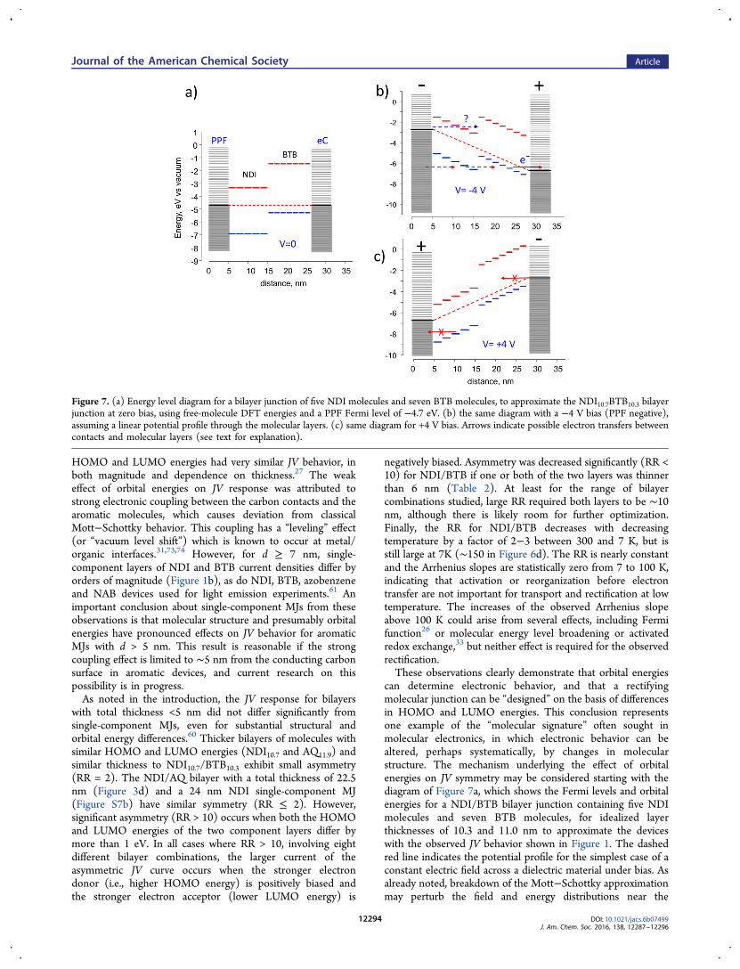
can determine electronic behavior, and that a rectifyingmolecular junction can be “designed” on the basis of differencesin HOMO and LUMO energies. This conclusion representsone example of the “molecular signature” often sought inmolecular electronics, in which electronic behavior can bealtered, perhaps systematically, by changes in molecularstructure. The mechanism underlying the effect of orbitalenergies on JV symmetry may be considered starting with thediagram of Figure 7a, which shows the Fermi levels and orbitalenergies for a NDI/BTB bilayer junction containing five NDImolecules and seven BTB molecules, for idealized layerthicknesses of 10.3 and 11.0 nm to approximate the deviceswith the observed JV behavior shown in Figure 1. The dashedred line indicates the potential profile for the simplest case of aconstant electric field across a dielectric material under bias. Asalready noted, breakdown of the Mott−Schottky approximationmay perturb the field and energy distributions near the
Figure 7. (a) Energy level diagram for a bilayer junction of five NDI molecules and seven BTB molecules, to approximate the NDI10.7BTB10.3 bilayerjunction at zero bias, using free-molecule DFT energies and a PPF Fermi level of −4.7 eV. (b) the same diagram with a −4 V bias (PPF negative),assuming a linear potential profile through the molecular layers. (c) same diagram for +4 V bias. Arrows indicate possible electron transfers betweencontacts and molecular layers (see text for explanation).
Journal of the American Chemical Society Article
DOI: 10.1021/jacs.6b07499J. Am. Chem. Soc. 2016, 138, 12287−12296
12294

contacts, but the diagram ignores that effect for simplicity. Theweak temperature dependence of both J and RR, particularlybelow 200 K, indicates that thermal population of the LUMOor Marcus-like reorganization before electron transfer areunlikely to be involved significantly in transport. As shown inFigure 7b, the high electric field under bias (∼2 MV/cm for V =−4 V), is predicted to cause significant shifts in orbital energiesdue to the linear potential profile altering the local electrostaticpotential of each molecule in the bilayer. A bias of −4 V (withPPF negative) could raise the HOMO energies of moleculesclose to the eC contact and permit transport from a HOMOinto empty eC orbitals, as indicated by the solid red arrow in7B. Such transport could be by tunneling or field ionization,33
but in either case the distance is much shorter than the 21 nmbilayer thickness. One possibility for continued transport isshown by the dashed red arrows, with the net result beingtransport from PPF to eC through the molecular HOMOs. Theopposite bias of +4 V as shown in Figure 7c indicates a quitedifferent situation. Electrons in the NDI HOMO cannottransfer into the filled PPF orbitals, nor can electrons in eCreach empty BTB orbitals. Note that this simple model reliesonly on the differences in frontier orbital energies of themolecular layers, since the Fermi levels of the carbon contactsare nominally equal. Therefore, bilayers made from twomolecules with similar HOMO and LUMO energies (e.g.,NDI/AQ) yield nearly symmetric JV response, while reversingthe order of the two layers in AQ/FL or AQ/BTB causesreversal of the direction of rectification.As already noted, in all rectifying bilayers (with RR > 10), the
larger junction current was observed when the strongerelectron acceptor was biased negative and the stronger donorwas biased positive. The concept of “injection” often used inorganic electronics applies to the current devices, but withsome limitations. The higher currents correspond to the lower“injection” barriers for the rectifiers, but this process is notthermally activated, and can occur at either PPF or eCinterfaces with the bilayer. Asymmetry is not the result ofdifferent contact work functions, as is often the case for organicp−n junctions with much thicker layers. “Injection” in thecurrent devices is likely field driven and operative even at lowtemperature, with RR constant from 7 to 200 K. Previousreports based on transport26 and photocurrents63,75 indicatedthat transport in several aromatic carbon-based MJs with d < 5nm is hole mediated, meaning the important barrier is thatbetween the molecular HOMO and the contact Fermi level. Anexception is NDI, which exhibits photocurrents consistent withLUMO mediation.63 While the observed RR roughly correlateswith the HOMO to Fermi Level offset, it also does to theLUMO to Ef offset. Figure 7b also shows an electrontransported from PPF to the NDI LUMO (dashed bluearrow), resulting in similar rectification. The current resultsclearly indicate that molecular structure and orbital energies canaffect the electronic behavior of bilayer molecular junctions, butadditional examples are necessary to identify which orbitals areinvolved. In addition, the mechanism of Figure 7 applies tobilayers which are made entirely from conjugated molecules,and lack the mix of aliphatic and aromatic components in whichrectification is observed in alkyl ferrocene molecularjunctions.15,17,40 The larger variation in orbital energies anddielectric constant of the latter devices may result in a quitedifferent rectification mechanism.In conclusion, the results provide a “molecular signature”
that exhibits significant changes in electronic behavior with
variation of molecular structure. In all cases studied, themolecular layers were thicker than the approximately 5 nm overwhich strong electronic coupling with the carbon contact isobserved, where the aforementioned “leveling” effect decreasesthe effect of orbital energy variation.27 While the rectificationdirection is similar to that observed for much thicker organic“p−n” junctions, the mechanism does not involve the same“injection” present in organic light emitting diodes, and it doesnot require contacts with different work functions. As is likelyalso the case for unimolecular rectifiers, the nanoscale transportdistances and high electric fields of the current devices enabletransport mechanisms not operative in conventional organicelectronics in films with thicknesses greater than 100 nm.
■ ASSOCIATED CONTENT*S Supporting InformationThe Supporting Information is available free of charge on theACS Publications website at DOI: 10.1021/jacs.6b07499.
Junction fabrication details, optical and XPS spectra, andadditional JV curves (PDF)
■ AUTHOR INFORMATIONCorresponding Author*[email protected] authors declare no competing financial interest.
■ ACKNOWLEDGMENTSThis work was supported by the University of Alberta, theNational Research Council of Canada, the National Science andEngineering Research Council and Alberta Innovates. ANR(France) is gratefully acknowledged for its financial support ofthis work (ANR-15-CE09 0001-01). We thank MykolaKondratenko for NDI synthesis, Amin Morteza-Najarian forAQ and FL diazonium synthesis and Bryan Szeto for expertassistance with LabView programming and device fabrication.
■ REFERENCES(1) Xiang, D.; Wang, X.; Jia, C.; Lee, T.; Guo, X. Chem. Rev. 2016,116, 4318−4440.(2) Metzger, R. M. Chem. Rev. 2015, 115, 5056−5115.(3) McCreery, R.; Yan, H.; Bergren, A. J. Phys. Chem. Chem. Phys.2013, 15, 1065−1081.(4) Amdursky, N.; Marchak, D.; Sepunaru, L.; Pecht, I.; Sheves, M.;Cahen, D. Adv. Mater. 2014, 26, 7142−7161.(5) Yoon, H. J.; Shapiro, N. D.; Park, K. M.; Thuo, M. M.; Soh, S.;Whitesides, G. M. Angew. Chem., Int. Ed. 2012, 51, 4658−4661.(6) Dickey, M. D.; Chiechi, R. C.; Larsen, R. J.; Weiss, E. A.; Weitz,D. A.; Whitesides, G. M. Adv. Funct. Mater. 2008, 18, 1097−1104.(7) Tran, E.; Duati, M.; Mullen, K.; Zharnikov, M.; Whitesides, G.M.; Rampi, M. Adv. Mater. 2006, 18, 1323.(8) Bowers, C. M.; Zhang, M.; Lyubarskaya, Y.; Toone, E. J.; Tang,C.; Shestopalov, A. A. Adv. Mater. Interfaces 2014, 1, 1300109.(9) Finklea, H. O. Electrochemistry of Organized Monolayers ofThiols and Related Molecules on Electrodes. In ElectroanalyticalChemistry; Bard, A. J., Ed.; Dekker: New York, 1996; Vol. 19, pp 109−335.(10) Finklea, H. O.; Hanshew, D. D. J. Am. Chem. Soc. 1992, 114,3173−3181.(11) Smalley, J. F.; Finkea, H. O.; Chidsey, C. E. D.; Linford, M. R.;Creager, S. E.; Ferraris, J. P.; Chalfant, K.; Zawodzinsk, T.; Feldberg, S.W.; Newton, M. D. J. Am. Chem. Soc. 2003, 125, 2004−2013.(12) Smalley, J. F.; Feldberg, S. W.; Chidsey, C. E. D.; Linford, M. R.;Newton, M. D.; Liu, Y.-P. J. Phys. Chem. 1995, 99, 13141−13149.
Journal of the American Chemical Society Article
DOI: 10.1021/jacs.6b07499J. Am. Chem. Soc. 2016, 138, 12287−12296
12295

(13) Chidsey, C. E. D. Science 1991, 251, 919−923.(14) Polo, F.; Antonello, S.; Formaggio, F.; Toniolo, C.; Maran, F. J.Am. Chem. Soc. 2004, 127, 492−493.(15) Yuan, L.; Nerngchamnong, N.; Cao, L.; Hamoudi, H.; del Barco,E.; Roemer, M.; Sriramula, R. K.; Thompson, D.; Nijhuis, C. A. Nat.Commun. 2015, 6, 7324.(16) Yuan, L.; Breuer, R.; Jiang, L.; Schmittel, M.; Nijhuis, C. A. NanoLett. 2015, 15, 5506−5512.(17) Nijhuis, C. A.; Reus, W. F.; Whitesides, G. M. J. Am. Chem. Soc.2009, 131, 17814−17827.(18) Chabinyc, M. L.; Chen, X.; Holmlin, R.; Jacobs, H.; Skulason,H.; Frisbie, C. D.; Mujica, V.; Ratner, M.; Rampi, M. A.; Whitesides, G.M. J. Am. Chem. Soc. 2002, 124, 11730−11736.(19) Hihath, J.; Bruot, C.; Nakamura, H.; Asai, Y.; Díez-Perez, I.; Lee,Y.; Yu, L.; Tao, N. ACS Nano 2011, 5, 8331−8339.(20) Yoon, H. P.; Maitani, M. M.; Cabarcos, O. M.; Cai, L.; Mayer, T.S.; Allara, D. L. Nano Lett. 2010, 10, 2897−2902.(21) Leng, J.-C.; Lin, L. L.; Song, X.-N.; Li, Z.-L.; Wang, C.-K. J. Phys.Chem. C 2009, 113, 18353−18357.(22) Yu, L. H.; Zangmeister, C. D.; Kushmerick, J. G. Phys. Rev. Lett.2007, 98, 206803−206804.(23) Honciuc, A.; Metzger, R. M.; Gong, A.; Spangler, C. W. J. Am.Chem. Soc. 2007, 129, 8310−8319.(24) Luo, L.; Choi, S. H.; Frisbie, C. D. Chem. Mater. 2011, 23, 631−645.(25) Choi, S. H.; Kim, B.; Frisbie, C. D. Science 2008, 320, 1482−1486.(26) Bergren, A. J.; McCreery, R. L.; Stoyanov, S. R.; Gusarov, S.;Kovalenko, A. J. Phys. Chem. C 2010, 114, 15806−15815.(27) Sayed, S. Y.; Fereiro, J. A.; Yan, H.; McCreery, R. L.; Bergren, A.J. Proc. Natl. Acad. Sci. U. S. A. 2012, 109, 11498−11503.(28) Xie, Z.; Baldea, I.; Smith, C. E.; Wu, Y.; Frisbie, C. D. ACS Nano2015, 9, 8022−8036.(29) Kim, B.; Choi, S. H.; Zhu, X. Y.; Frisbie, C. D. J. Am. Chem. Soc.2011, 133, 19864−19877.(30) Yaffe, O.; Qi, Y. B.; Scheres, L.; Puniredd, S. R.; Segev, L.; Ely,T.; Haick, H.; Zuilhof, H.; Vilan, A.; Kronik, L.; Kahn, A.; Cahen, D.Phys. Rev. B: Condens. Matter Mater. Phys. 2012, 85, 045433.(31) Vilan, A.; Yaffe, O.; Biller, A.; Salomon, A.; Kahn, A.; Cahen, D.Adv. Mater. 2010, 22, 140−159.(32) Cahen, D.; Kahn, A. Adv. Mater. 2003, 15, 271−277.(33) Yan, H.; Bergren, A. J.; McCreery, R.; Della Rocca, M. L.;Martin, P.; Lafarge, P.; Lacroix, J. C. Proc. Natl. Acad. Sci. U. S. A. 2013,110, 5326−5330.(34) Choi, S. H.; Risko, C.; Delgado, M. C. R.; Kim, B.; Bredas, J.-L.;Frisbie, C. D. J. Am. Chem. Soc. 2010, 132, 4358−4368.(35) Aviram, A.; Ratner, M. Chem. Phys. Lett. 1974, 29, 277−283.(36) Elbing, M.; Ochs, R.; Koentopp, M.; Fischer, M.; von Hanisch,C.; Weigend, F.; Evers, F.; Weber, H. B.; Mayor, M. Proc. Natl. Acad.Sci. U. S. A. 2005, 102, 8815−8820.(37) Stadler, R.; Geskin, V.; Cornil, J. J. Phys.: Condens. Matter 2008,20, 374105.(38) Berlin, Y. A.; Grozema, F. C.; Siebbeles, L. D. A.; Ratner, M. A.J. Phys. Chem. C 2008, 112, 10988−11000.(39) Nijhuis, C. A.; Reus, W. F.; Siegel, A. C.; Whitesides, G. M. J.Am. Chem. Soc. 2011, 133, 15397−15411.(40) Nijhuis, C. A.; Reus, W. F.; Whitesides, G. M. J. Am. Chem. Soc.2010, 132, 18386−18401.(41) Van Dyck, C.; Ratner, M. A. Nano Lett. 2015, 15, 1577−1584.(42) Fluteau, T.; Bessis, C.; Barraud, C.; Della Rocca, M. L.; Martin,P.; Lacroix, J.-C.; Lafarge, P. J. Appl. Phys. 2014, 116, 114509.(43) Martin, P.; Della Rocca, M. L.; Anthore, A.; Lafarge, P.; Lacroix,J.-C. J. Am. Chem. Soc. 2012, 134, 154−157.(44) Kuikka, M. A.; Li, W.; Kavanagh, K. L.; Yu, H.-Z. J. Phys. Chem.C 2008, 112, 9081−9088.(45) Zhao, J.; Yu, C.; Wang, N.; Liu, H. J. Phys. Chem. C 2010, 114,4135−4141.
(46) Capozzi, B.; Xia, J.; Adak, O.; Dell, E. J.; Liu, Z.-F.; Taylor, J. C.;Neaton, J. B.; Campos, L. M.; Venkataraman, L. Nat. Nanotechnol.2015, 10, 522−527.(47) Zhang, W.; Zhang, X.; Lu, C.; Wang, Y.; Deng, Y. J. Phys. Chem.C 2012, 116, 9227−9234.(48) Jin, Y.; Friedman, N.; Sheves, M.; Cahen, D. Langmuir 2008, 24,5622−5626.(49) Yu, X.; Lovrincic, R.; Kraynis, O.; Man, G.; Ely, T.; Zohar, A.;Toledano, T.; Cahen, D.; Vilan, A. Small 2014, 10, 5151−5160.(50) Li, Y.; Calder, S.; Yaffe, O.; Cahen, D.; Haick, H.; Kronik, L.;Zuilhof, H. Langmuir 2012, 28, 9920−9929.(51) Popoff, R. T. W.; Zavareh, A. A.; Kavanagh, K. L.; Yu, H.-Z. J.Phys. Chem. C 2012, 116, 17040−17047.(52) Popoff, R. T. W.; Asanuma, H.; Yu, H.-Z. J. Phys. Chem. C 2010,114, 10866−10872.(53) Zhu, L.; Popoff, R. T. W.; Yu, H.-Z. J. Phys. Chem. C 2015, 119,1826−1831.(54) Kleemann, H.; Gutierrez, R.; Avdoshenko, S.; Cuniberti, G.;Leo, K.; Lussem, B. Org. Electron. 2013, 14, 193−199.(55) Kleemann, H.; Gutierrez, R.; Lindner, F.; Avdoshenko, S.;Manrique, P. D.; LuI ssem, B. r.; Cuniberti, G.; Leo, K. Nano Lett.2010, 10, 4929−4934.(56) Sengoku, T.; Yamao, T.; Hotta, S. J. Non-Cryst. Solids 2012, 358,2525−2529.(57) Saracco, E.; Bouthinon, B.; Verilhac, J.-M.; Celle, C.; Chevalier,N.; Mariolle, D.; Dhez, O.; Simonato, J.-P. Adv. Mater. 2013, 25,6534−6538.(58) Kong, H.; Sinha, J.; Hoeft, D.; Kirschner, S. B.; Reich, D. H.;Katz, H. E. Org. Electron. 2013, 14, 703−710.(59) Gong, X.; Tong, M.; Xia, Y.; Cai, W.; Moon, J. S.; Cao, Y.; Yu,G.; Shieh, C.-L.; Nilsson, B.; Heeger, A. J. Science 2009, 325, 1665−1667.(60) Sayed, S. Y.; Bayat, A.; Kondratenko, M.; Leroux, Y.; Hapiot, P.;McCreery, R. L. J. Am. Chem. Soc. 2013, 135, 12972−12975.(61) Ivashenko, O.; Bergren, A. J.; McCreery, R. L. J. Am. Chem. Soc.2016, 138, 722−725.(62) Yan, H.; Bergren, A. J.; McCreery, R. L. J. Am. Chem. Soc. 2011,133, 19168−19177.(63) Fereiro, J. A.; Kondratenko, M.; Bergren, A. J.; McCreery, R. L.J. Am. Chem. Soc. 2015, 137, 1296−1304.(64) Fave, C.; Leroux, Y.; Trippe, G.; Randriamahazaka, H.; Noel, V.;Lacroix, J.-C. J. Am. Chem. Soc. 2007, 129, 1890−1891.(65) Santos, L.; Ghilane, J.; Lacroix, J. C. J. Am. Chem. Soc. 2012, 134,5476−5479.(66) Anariba, F.; DuVall, S. H.; McCreery, R. L. Anal. Chem. 2003,75, 3837−3844.(67) Hurley, B. L.; McCreery, R. L. J. Electrochem. Soc. 2004, 151,B252.(68) Belanger, D.; Pinson, J. Chem. Soc. Rev. 2011, 40, 3995−4048.(69) Stockhausen, V.; Trippe-Allard, G.; Van Quynh, N.; Ghilane, J.;Lacroix, J.-C. J. Phys. Chem. C 2015, 119, 19218−19227.(70) Bergren, A. J.; McCreery, R. L. Annu. Rev. Anal. Chem. 2011, 4,173−195.(71) Ru, J.; Szeto, B.; Bonifas, A.; McCreery, R. L. ACS Appl. Mater.Interfaces 2010, 2, 3693−3701.(72) Anariba, F.; Viswanathan, U.; Bocian, D. F.; McCreery, R. L.Anal. Chem. 2006, 78, 3104−3112.(73) Hwang, J.; Wan, A.; Kahn, A. Mater. Sci. Eng., R 2009, 64, 1−31.(74) Braun, S.; Salaneck, W. R.; Fahlman, M. Adv. Mater. 2009, 21,1450−1472.(75) Fereiro, J. A.; McCreery, R. L.; Bergren, A. J. J. Am. Chem. Soc.2013, 135, 9584−9587.
Journal of the American Chemical Society Article
DOI: 10.1021/jacs.6b07499J. Am. Chem. Soc. 2016, 138, 12287−12296
12296