continuous digital calibration of pipelined a/d …web.eece.maine.edu/~hummels/thesis/adi_04.pdf ·...
TRANSCRIPT

CONTINUOUS DIGITAL CALIBRATION OF PIPELINED A/D
CONVERTERS
By
Alma Delic-Ibukic
B.S. University of Maine, 2002
A THESIS
Submitted in Partial Fulfillment of the
Requirements for the Degree of
Master of Science
(in Electrical Engineering)
The Graduate School
The University of Maine
May, 2004
Advisory Committee:
Donald M. Hummels, Professor of Electrical and Computer Engineering, Advisor
David E. Kotecki, Associate Professor of Electrical and Computer Engineering
Allison I. Whitney, Lecturer in Electrical and Computer Engineering

LIBRARY RIGHTS STATEMENT
In presenting this thesis in partial fulfillment of the requirements for an advanced
degree at The University of Maine, I agree that the Library shall make it freely available
for inspection. I further agree that permission for “fair use” copying of this thesis for
scholarly purposes may be granted by the Librarian. It is understood that any copying
or publication of this thesis for financial gain shall not be allowed without my written
permission.
Signature:
Date:
CONTINUOUS DIGITAL CALIBRATION OF PIPELINED A/D
CONVERTERS
By Alma Delic-Ibukic
Thesis Advisor: Dr. Donald M. Hummels
An Abstract of the Thesis Presentedin Partial Fulfillment of the Requirements for the
Degree of Master of Science(in Electrical Engineering)
May, 2004
This thesis provides a novel continuous calibration technique for pipelined Analog-to-
Digital Converters (ADCs). The new scheme utilizes an existing digital calibration
algorithm and extends it to work in real-time. The goal is to digitally calibrate pipelined
ADCs in the background without interrupting the normal operation of the converter.
The concept behind the digital calibration algorithm is described and simulated
using a 1-bit per stage pipeline architecture. Dominant static error mechanisms present
in pipeline architectures are identified and discussed. These errors are successfully
corrected by the implemented digital calibration algorithm. The calibration scheme is
transparent to the overall system performance and is demonstrated using a 14-bit ADC
with 1-bit per stage architecture and 16 identical stages. The first seven stages in the
pipeline are calibrated. Continuous calibration is realized using a hardware description
language (Verilog HDL) and two extra stages located at the end of the pipeline. The
extra stages are only used during the calibration process. Verilog implementations of
stage and error correction logic, as well as a finite state machine to control the calibration
process are presented.
The real-time digital calibration technique is verified and successfully demon-
strated using simulation results obtained in MATLAB and the Verilog-XL simulator.

ACKNOWLEDGMENTS
The work described in this thesis has been supported in part through a gift from
the Texas Instruments Inc. Analog University Relations program. The department grate-
fully acknowledges the support of its undergraduate and graduate programs provided by
Texas Instruments Inc. through this program.
I would first like to thank my parents, Nihada and Sead Delic-Ibukic and my
brother Dino for their love, support and encouragement throughout this educational
endeavor. I would also like to thank Professor Don Hummels for being a great mentor
throughout my bachelor’s and master’s degree and for introducing me to data converters.
Thank you, Professor Fred Irons for finding time to review my thesis and providing
helpful comments. Thank you, Professor Dave Kotecki for patiently answering all my
Cadence and Verilog questions. Thank you, Professor Al Whitney for encouraging me
to take electronics classes and always being available to answer any questions I had.
Thank you, Steven Turner, Wayne Slade and Thomas Kenny for being great
friends. Who can forget all those quality times spent at the Bear Brew.
University of Maine MS ThesisAlma Delic-Ibukic, May, 2004
ii

TABLE OF CONTENTS
ACKNOWLEDGMENTS .. . . . . . . . . . . . . . . . . . . . . . . . . . . . . . . . . . . . . . . . . . . . . . . . . . . . . . . . . . . . .ii
LIST OF TABLES.. . . . . . . . . . . . . . . . . . . . . . . . . . . . . . . . . . . . . . . . . . . . . . . . . . . . . . . . . . . . . . . . . . . . . .v
LIST OF FIGURES.. . . . . . . . . . . . . . . . . . . . . . . . . . . . . . . . . . . . . . . . . . . . . . . . . . . . . . . . . . . . . . . . . . . .vi
Chapter
1 Introduction. . . . . . . . . . . . . . . . . . . . . . . . . . . . . . . . . . . . . . . . . . . . . . . . . . . . . . . . . . . . . . . . . . . . . . . . . .11.1 Background. . . . . . . . . . . . . . . . . . . . . . . . . . . . . . . . . . . . . . . . . . . . . . . . . . . . . . . . . . . . . . . . . . .11.2 Purpose of the Research. . . . . . . . . . . . . . . . . . . . . . . . . . . . . . . . . . . . . . . . . . . . . . . . . . . . . .21.3 Thesis Organization. . . . . . . . . . . . . . . . . . . . . . . . . . . . . . . . . . . . . . . . . . . . . . . . . . . . . . . . . . .3
2 Pipelined ADC Architecture. . . . . . . . . . . . . . . . . . . . . . . . . . . . . . . . . . . . . . . . . . . . . . . . . . . . . . . .52.1 Architecture Overview. . . . . . . . . . . . . . . . . . . . . . . . . . . . . . . . . . . . . . . . . . . . . . . . . . . . . . . .52.2 Ideal Pipeline Converter. . . . . . . . . . . . . . . . . . . . . . . . . . . . . . . . . . . . . . . . . . . . . . . . . . . . . .72.3 Design Considerations for Pipeline ADCs. . . . . . . . . . . . . . . . . . . . . . . . . . . . . . . . . . .10
2.3.1 Sub-ADC Error. . . . . . . . . . . . . . . . . . . . . . . . . . . . . . . . . . . . . . . . . . . . . . . . . . . . . . .102.3.2 One Bit per Stage Example. . . . . . . . . . . . . . . . . . . . . . . . . . . . . . . . . . . . . . . . . .14
3 Pipeline A/D Converter Calibration Techniques. . . . . . . . . . . . . . . . . . . . . . . . . . . . . . . . . . .183.1 Dominant Errors in Pipeline ADCs. . . . . . . . . . . . . . . . . . . . . . . . . . . . . . . . . . . . . . . . . .18
3.1.1 Sub-DAC Error. . . . . . . . . . . . . . . . . . . . . . . . . . . . . . . . . . . . . . . . . . . . . . . . . . . . . . .203.1.2 Gain Error. . . . . . . . . . . . . . . . . . . . . . . . . . . . . . . . . . . . . . . . . . . . . . . . . . . . . . . . . . . .21
3.2 Analog Calibration Schemes. . . . . . . . . . . . . . . . . . . . . . . . . . . . . . . . . . . . . . . . . . . . . . . . .233.3 Digital Calibration Schemes. . . . . . . . . . . . . . . . . . . . . . . . . . . . . . . . . . . . . . . . . . . . . . . . . .253.4 Digital Calibration Example: 1-bit per stage. . . . . . . . . . . . . . . . . . . . . . . . . . . . . . . .26
3.4.1 Off-line Calibration. . . . . . . . . . . . . . . . . . . . . . . . . . . . . . . . . . . . . . . . . . . . . . . . . .273.4.2 Simulation Results. . . . . . . . . . . . . . . . . . . . . . . . . . . . . . . . . . . . . . . . . . . . . . . . . . .30
3.5 Real-Time Digital Calibration Scheme Development. . . . . . . . . . . . . . . . . . . . . . .39
4 Implementation of a Continuous Digital Calibration Scheme in VerilogHDL . . . . . . . . . . . . . . . . . . . . . . . . . . . . . . . . . . . . . . . . . . . . . . . . . . . . . . . . . . . . . . . . . . . . . . . . . . . . . . . . . .504.1 Digital Calibration in Verilog HDL. . . . . . . . . . . . . . . . . . . . . . . . . . . . . . . . . . . . . . . . . .50
4.1.1 Finite State Machine (FSM) Description. . . . . . . . . . . . . . . . . . . . . . . . . . .504.1.2 Required Stage Modifications. . . . . . . . . . . . . . . . . . . . . . . . . . . . . . . . . . . . . . .554.1.3 Error Correction Logic Modification. . . . . . . . . . . . . . . . . . . . . . . . . . . . . . . .55
4.2 Verification of the Developed Calibration Technique. . . . . . . . . . . . . . . . . . . . . . .574.3 Complexity of the Real-Time Calibration Logic. . . . . . . . . . . . . . . . . . . . . . . . . . . .63
5 Conclusion. . . . . . . . . . . . . . . . . . . . . . . . . . . . . . . . . . . . . . . . . . . . . . . . . . . . . . . . . . . . . . . . . . . . . . . . . . .66
University of Maine MS ThesisAlma Delic-Ibukic, May, 2004
iii

REFERENCES.. . . . . . . . . . . . . . . . . . . . . . . . . . . . . . . . . . . . . . . . . . . . . . . . . . . . . . . . . . . . . . . . . . . . . . . . .68
BIOGRAPHY OF THE AUTHOR.. . . . . . . . . . . . . . . . . . . . . . . . . . . . . . . . . . . . . . . . . . . . . . . . . . . .70
University of Maine MS ThesisAlma Delic-Ibukic, May, 2004
iv

LIST OF TABLES
3.1 Parameters for simulated 14-bit Pipeline ADC (units in volts).. . . . . . . . . . 36
3.2 Sample propagation through the pipeline for the proposed real-time digital calibration technique.. . . . . . . . . . . . . . . . . . . . . . . . . . . . . . . . . . . . . . . . .46
4.1 Weights associated with each stage of a 14-bit calibrated pipelineADC. Values inred correspond to the programmable set ofweights. . . . . . . . . . . . . . . . . . . . . . . . . . . . . . . . . . . . . . . . . . . . . . . . . . . . . . . . . . . . . . . . . . . . . .54
University of Maine MS ThesisAlma Delic-Ibukic, May, 2004
v

LIST OF FIGURES
2.1 Generic Pipeline ADC block diagram.. . . . . . . . . . . . . . . . . . . . . . . . . . . . . . . . . . 6
2.2 Generic stage block diagram.. . . . . . . . . . . . . . . . . . . . . . . . . . . . . . . . . . . . . . . . . . . .7
2.3 AnM -bit ADC. . . . . . . . . . . . . . . . . . . . . . . . . . . . . . . . . . . . . . . . . . . . . . . . . . . . . . . . . . .8
2.4 AnN -bit ADC connected to anM -bit ADC. . . . . . . . . . . . . . . . . . . . . . . . . . . 8
2.5 AnM + N bit ideal ADC. . . . . . . . . . . . . . . . . . . . . . . . . . . . . . . . . . . . . . . . . . . . . . .10
2.6 AnN -bit ideal ADC with 1-bit per stage architecture.. . . . . . . . . . . . . . . . 11
2.7 Residual error plot for 1-bit per stage ideal pipeline ADC(blue) and pipeline ADC with comparator offset errors (red).. . . . . . . . . . 12
2.8 Stage modifications of 1-bit per stage architecture pipelineADC (blue) with allowable comparator offset errors (red). . . . . . . . . . . . . 13
2.9 1-bit per stage architecture block diagram.. . . . . . . . . . . . . . . . . . . . . . . . . . . . .14
2.10 Residual error characteristics and allowed threshold voltagevariations. . . . . . . . . . . . . . . . . . . . . . . . . . . . . . . . . . . . . . . . . . . . . . . . . . . . . . . . . . . . . . . . .17
3.1 Residual error plots for 1-bit per stage ideal pipeline ADC(blue) and pipeline ADC with errors (red). . . . . . . . . . . . . . . . . . . . . . . . . . . . . . .19
3.2 1-bit per stage architecture block diagram.. . . . . . . . . . . . . . . . . . . . . . . . . . . . .21
3.3 Switched capacitor implementation of the MDAC for 1-bitper stage architecture.. . . . . . . . . . . . . . . . . . . . . . . . . . . . . . . . . . . . . . . . . . . . . . . . . . . .22
3.4 Pipeline ADC with off-line digital calibration applied to theseventh stage.. . . . . . . . . . . . . . . . . . . . . . . . . . . . . . . . . . . . . . . . . . . . . . . . . . . . . . . . . . . . .28
3.5 Residual plot for 1.5-bits per stage pipeline architecture.. . . . . . . . . . . . . . 31
3.6 Simulated 14-bit pipeline (ideal) ADC withFin = 1 MHz. . . . . . . . . . . . . 32
3.7 Calibrated vs. uncalibrated residual error for a simulatedpipeline (ideal) ADC.. . . . . . . . . . . . . . . . . . . . . . . . . . . . . . . . . . . . . . . . . . . . . . . . . . . . .34
3.8 Locations of parameters for simulated ADC.. . . . . . . . . . . . . . . . . . . . . . . . . . .36
3.9 Simulated ADC output spectrum with (red) and without(blue) digital self-calibration applied.. . . . . . . . . . . . . . . . . . . . . . . . . . . . . . . . . . .37
3.10 Simulated ADC output spectrum with (red) and without(blue) digital self-calibration appliedcont.. . . . . . . . . . . . . . . . . . . . . . . . . . . . . .38
University of Maine MS ThesisAlma Delic-Ibukic, May, 2004
vi

3.11 Simulated ADC residual error characteristics with (red) andwithout (blue) digital self-calibration applied. Errors intro-duced in a first stage.. . . . . . . . . . . . . . . . . . . . . . . . . . . . . . . . . . . . . . . . . . . . . . . . . . . . .40
3.12 Simulated ADC residual error characteristics with (red) andwithout (blue) digital self-calibration applied. Errors intro-duced in a first two stages.. . . . . . . . . . . . . . . . . . . . . . . . . . . . . . . . . . . . . . . . . . . . . . .41
3.13 Simulated ADC residual error characteristics with (red) andwithout (blue) digital self-calibration applied. Errors intro-duced in a first three stages.. . . . . . . . . . . . . . . . . . . . . . . . . . . . . . . . . . . . . . . . . . . . . .42
3.14 Simulated ADC residual error characteristics with (red) andwithout (blue) digital self-calibration applied. Errors intro-duced in a first seven stages.. . . . . . . . . . . . . . . . . . . . . . . . . . . . . . . . . . . . . . . . . . . . .43
3.15 Example of a two-phase, non-overlapping clock signal usedin pipeline ADC architecture.. . . . . . . . . . . . . . . . . . . . . . . . . . . . . . . . . . . . . . . . . . .44
3.16 Proposed real-time digital calibration architecture.. . . . . . . . . . . . . . . . . . . . . 48
4.1 Simplified description of the sequence of events implementedby the master Finite State Machine (FSM).. . . . . . . . . . . . . . . . . . . . . . . . . . . . .52
4.2 Modifications of a stage being calibrated.. . . . . . . . . . . . . . . . . . . . . . . . . . . . . .56
4.3 Modified error correction logic for a real-time digital calibrationscheme implementation. Example ofN -stage converter with1-bit per stage architecture.. . . . . . . . . . . . . . . . . . . . . . . . . . . . . . . . . . . . . . . . . . . . . . .58
4.4 Residual error characteristics for a MATLAB simulated ADCwith applied foreground calibration (blue) and real-time calibrationimplemented in Verilog HDL (red).. . . . . . . . . . . . . . . . . . . . . . . . . . . . . . . . . . . . . .61
4.5 Residual error characteristics for a MATLAB simulated ADCwith applied foreground calibration (blue) and real-time calibrationimplemented in Verilog HDL (red) cont.. . . . . . . . . . . . . . . . . . . . . . . . . . . . . . . .62
4.6 Residual error characteristics for a converter with errors ina first stage only and real-time calibration applied twice.. . . . . . . . . . . . . . 64
4.7 Area of the real-time calibration logic as a function of aminimum feature size requirements.. . . . . . . . . . . . . . . . . . . . . . . . . . . . . . . . . . . .65
University of Maine MS ThesisAlma Delic-Ibukic, May, 2004
vii

CHAPTER 1
Introduction
1.1 Background
Applications such as wireless communications, image recognition and medical
instrumentation require high-speed, high-resolution Analog-to-Digital Converters (ADCs).
Medical imaging applications require ADCs with 15 bits of resolution and sampling
rates greater than 40 MHz [1]. High-speed and high resolution converters are often
implemented using pipelined multistage ADC architectures. In many cases, this is
the architecture of choice because finite op-amp gain and comparator offset errors of
the converter can be removed by using redundancy [2] and digital error correction.
Also, the hardware complexity of the pipeline converter is proportional to the number
of bits resolved. Designs of pipelined architecture ADCs have relied on high-gain
operational amplifiers and excellent capacitor matching in order to produce moderate-
resolution converters. Monolithic, high-resolution pipeline ADCs are difficult to obtain
due to extraordinary component matching requirements. Component matching becomes
increasingly difficult as CMOS technologies are scaled to smaller geometries. Without
using some form of calibration, standard CMOS process technologies limit the resolution
of pipeline architecture to approximately 8-10 bits.
Different calibration techniques have been proposed to improve speed and linearity
of ADCs. Calibration techniques can be of analog nature [3], digital nature [4, 5]
or mixed (analog and digital) nature [6, 7, 8]. Most calibration techniques fall into
one of three categories: calibration performed in a factory, calibration performed every
time converter is powered up (foreground calibration) [4, 6, 9, 10, 11], and continuous
calibration [3, 8, 12]. Calibrations performed in a factory, such as capacitor trimming,
University of Maine MS ThesisAlma Delic-Ibukic, May, 2004
1

are one time events. Before packaging the ADC, capacitors are trimmed to accom-
plish the best possible capacitor matching and therefore improve the linearity of the
ADC. This type of calibration requires the converter to be off-line and it can not take
into account changes in the environment that may affect performance of the converter.
Factory calibrated converters cannot be re-calibrated. An advantage of the foreground
calibration is that re-calibration is possible. However, this requires a converter to be
off-line while (re)calibration is in progress. The ideal type of calibration is continuous
calibration because the converter is in its normal mode of operation while being calibrated.
Continuous calibration is done in the background without interrupting the ADC operation.
Environmental and internal changes are continuously taken into account and corrected.
Several analog continuous calibration schemes have been reported in the liter-
ature [3, 8]. Calibration techniques based on analog schemes are generally difficult to
scale to new process technologies, and are often specific to a particular circuit imple-
mentation. Shuet al. [12] reported a digital continuous calibration technique utilizing
a second on-chip delta-sigma ADC. However, the technique could not correct certain
dominant pipeline error mechanisms, such as error due to op-amp gain. This thesis
develops a novel continuous digital calibration technique suitable for implementation
in a fully monolithic pipeline ADC. The technique is based on a digital foreground
calibration algorithm originally reported in [4].
1.2 Purpose of the Research
Different calibration techniques targeted to pipelined ADCs have been proposed
and successfully implemented. Karanicolaset al. [4] implemented 15-bit digitally
self-calibrated pipeline ADC. The digital calibration algorithm was derived for a 1-bit
per stage pipeline architecture. The calibration was successful in correcting DAC and
interstage gain nonlinearities. Even though it proved to be successful, this calibration
technique required the converter to be off-line while calibrated. Ideally, a calibration
University of Maine MS ThesisAlma Delic-Ibukic, May, 2004
2

scheme should run continuously in the background without interrupting the normal
mode of operation of the ADC. A continuous calibration scheme was successfully employed
by Ingino et al. [3]. They performed calibration in the analog domain, transparent to
the overall system. An extra stage was implemented and calibrated outside of the main
converter pipeline. The additional stage was frequently substituted for the pipeline stage
being calibrated. The technique corrects for the DAC and interstage gain nonlinearities.
However, the analog calibration schemes are as a rule difficult to scale to new process
technologies due to the increase in sub-threshold and gate leakage currents and reduced
power supply voltage [13].
This thesis defines a novel calibration scheme unique to pipeline ADCs based
on the digital self-calibration implemented by Karanicolaset al. [4]. A state machine
is developed which allows for a continuous calibration in a fully digital domain. This
calibration is transparent to the overall system and is demonstrated using a 14-bit ADC
with 1-bit per stage pipeline architecture and interstage gains less than two. DAC and
interstage gain errors due to the charge injection and capacitor mismatch are corrected
successfully. The continuous digital calibration discussed in this thesis is realized using
a hardware description language (Verilog HDL). The two extra stages are located at the
end of the pipeline. The extra stages are only used during the calibration process.
1.3 Thesis Organization
This thesis is structured to provide some background information on pipelined
ADCs, followed by the theory, simulation and results of the implemented continuous
digital calibration technique.
Chapter 2 gives an overview of a pipeline ADC architecture using an ideal
converter as an example. Error mechanisms in the pipeline stage that can be fixed by
stage modifications are introduced and discussed. An example of 1-bit per stage pipeline
ADC is presented.
University of Maine MS ThesisAlma Delic-Ibukic, May, 2004
3

Chapter 3 describes the dominant errors in pipeline ADCs which cannot be
corrected by stage modifications alone. Some form of calibration is required to correct
these error mechanisms. Theory and examples of the current analog and digital calibration
schemes for the pipeline ADCs are discussed. An example of the digital calibration
algorithm derived in [4] is discussed in detail. MATLAB simulations for this algorithm
were implemented using a 14-bit, 1-bit per stage ADC with 16 identical stages with
gains less than two. Also, a proposed real-time digital calibration technique based on
the calibration algorithm in [4] is discussed in detail using the same 14-bit, 1-bit per
stage ADC example.
Chapter 4 describes the implementation of the continuous digital calibration
technique in Verilog HDL. Verification of the derived calibration technique is discussed
in detail, as well as the complexity of the derived calibration scheme.
Chapter 5 gives a summary of the thesis and a brief section on future work is
also included.
University of Maine MS ThesisAlma Delic-Ibukic, May, 2004
4

CHAPTER 2
Pipelined ADC Architecture
This chapter provides an overview of the pipeline architecture. The internal
behavior of the ideal converter and steps commonly taken to ensure the linearity of
ADCs are examined and discussed. An example 1-bit per stage architecture is used to
describe the behavior of pipeline ADCs.
2.1 Architecture Overview
High speed, high resolution, low power ADCs are frequently based on a pipeline
architecture. One of the reasons is that the overall speed of the pipeline converter is given
by the speed of the single low resolution stage.
A conventional pipeline converter architecture is shown in Figure2.1. Each
stage in the pipeline serves two purposes: to provideqi, the coarse resolution digital
representation of the input voltage and to provide the next stage in the pipeline withri,
the difference between the input voltage and analog form ofqi. This residual voltage,
ri, is passed on to the subsequent stages for quantization in an attempt to improve the
digital representation of the input. Allqi’s are collected in the digital encoder block
where they are combined properly to achieve a higher resolution representation of the
input voltageX.
All stages are referenced to the same clock. Once Stage 1 producesq1 andr1, the
next stage is ready to process the residual of Stage 1 while Stage 1 is ready to quantize
the next input sample. This continuous processing of samples by the subsequent stages
is the concept of pipelining. The final higher resolution digital output of the pipeline
converter is obtained once the last stage in the pipeline has quantized its given input
sample. Because the subsequent stages need to wait for the previous stages to process
the input sample, there is an inherent latency associated with the pipeline architecture.
University of Maine MS ThesisAlma Delic-Ibukic, May, 2004
5

Stage 2 Stage N
qnq
1 q2
Stage 1
Digital Output
Xr1 2r
Clock
Digital Encoder
Figure 2.1: Generic Pipeline ADC block diagram.
This latency increases with the number of additional stages. The inherent latency in the
pipeline architecture is acceptable for many applications which require the high speed
and low power consumption that the pipeline converter provides.
Figure2.2 shows a block diagram of a typical stage in a pipeline. The analog
input signal is sampled by the Sample and Hold (S/H) circuit. The sampled input
is converted to the coarse resolution of the stage by the low-resolution flash ADC
(sub-ADC). The sub-ADC outputqi is an integer value ranging from 0 to2Bi − 1. Once
the coarse digital representation of the input sample is obtained, the value is passed on
to the low-resolution DAC (sub-DAC) to form the coarse analog representation of the
same sample. This voltage is subtracted from the initial input sample giving the error
voltage,ei. The resulting error voltage,ei, is scaled by the gain factor and passed as
the residual,ri, to the next stage. The gain factor is selected so the error voltage of the
given stage is scaled to accommodate the acceptable input range of the next stage. For
an ideal sub-ADC and sub-DAC, the gain factor can be set toGi = 2Bi, whereBi is the
number of resolvable bits for the given stage. Selecting a gain factor as a power of two
simplifies the logic of the digital encoder block.
University of Maine MS ThesisAlma Delic-Ibukic, May, 2004
6

Bi( −bit)qi
−bitBi −bitBi
ri−1Gi
DAC
+−
+S/H
ADC
riie
Figure 2.2: Generic stage block diagram.
The number of stages in a pipelined converter varies as does the number of
resolvable bits per stage. Low resolution stages are easier to build and they don’t
occupy too much real-estate in silicon. In theory, a 2 bits per stage architecture would
require three comparators per stage, and a 4 bits per stage architecture would require
15 comparators per stage. The number of required pipeline stages is a function of the
desired final ADC resolution and the implemented resolution per stage. Low resolution
stages require more pipeline stages to obtain higher final ADC resolution and vice versa.
The following sections discuss typical internal behavior of ideal pipeline converters and
limitations which cause linearity degradation in their performance.
2.2 Ideal Pipeline Converter
A high resolution pipeline converter can be constructed using a pipeline of low
resolution ADCs and interstage gain blocks. To see how low resolution ADCs can be
pipelined to achieve higher resolution, consider anM -bit ADC that provides both a
digital output and residual voltage. Figure2.3 shows theM -bit ADC with the input
voltageX, digital outputq and residual voltagee. The input signal is assumed to range
from −VREF to +VREF , whereVREF represents the positive and negative input signal
swing. The quantization interval for theM -bit ADC is QM = 2VREF /2M . The integer
University of Maine MS ThesisAlma Delic-Ibukic, May, 2004
7
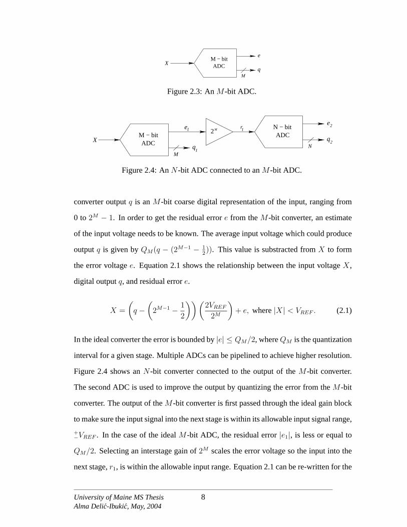
XM − bitADC
qM
e
Figure 2.3: AnM -bit ADC.
M − bitADC
qM
e2
X
1
1
2
2
r1M
q
e
ADC
N
N − bit
Figure 2.4: AnN -bit ADC connected to anM -bit ADC.
converter outputq is anM -bit coarse digital representation of the input, ranging from
0 to 2M − 1. In order to get the residual errore from theM -bit converter, an estimate
of the input voltage needs to be known. The average input voltage which could produce
outputq is given byQM(q − (2M−1 − 12)). This value is substracted fromX to form
the error voltagee. Equation2.1 shows the relationship between the input voltageX,
digital outputq, and residual errore.
X =
(q −
(2M−1 − 1
2
)) (2VREF
2M
)+ e, where|X| < VREF . (2.1)
In the ideal converter the error is bounded by|e| ≤ QM/2, whereQM is the quantization
interval for a given stage. Multiple ADCs can be pipelined to achieve higher resolution.
Figure2.4 shows anN -bit converter connected to the output of theM -bit converter.
The second ADC is used to improve the output by quantizing the error from theM -bit
converter. The output of theM -bit converter is first passed through the ideal gain block
to make sure the input signal into the next stage is within its allowable input signal range,
+−VREF . In the case of the idealM -bit ADC, the residual error|e1|, is less or equal to
QM/2. Selecting an interstage gain of2M scales the error voltage so the input into the
next stage,r1, is within the allowable input range. Equation2.1can be re-written for the
University of Maine MS ThesisAlma Delic-Ibukic, May, 2004
8

N -bit converter,
r1 =
(q2 −
(2N−1 − 1
2
)) (2VREF
2N
)+ e2, where|e2| ≤
QN
2=
VREF
2N. (2.2)
Sincer1 = 2Me1, (2.2) may be written in terms ofe1.
e1 =
(q2 −
(2N−1 − 1
2
)) (2VREF
2N+M
)+
e2
2M. (2.3)
By combining (2.3) and (2.1), an expression for the inputX and the quantized outputs
is obtained as
X =
(q12
N + q2 −(
2M+N−1 − 1
2
)) (2VREF
2M+N
)+
e2
2M, (2.4)
where the error of the ideal (M + N )-bit converter is bounded by
∣∣∣ e2
2M
∣∣∣ ≤ QN+M
2=
VREF
2N+M. (2.5)
By combining two ADCs, theN -bit andM -bit converters, a higher resolution estimate
for the input signal is obtained. This is due to the decrease in the overall quantization
interval of the combined converters. The new quantization interval obtained from (2.4)
is QN+M = 2VREF /2M+N . The digital representation of the input for the combined
converters is given byD = q12N + q2. The formation of the digital output is performed
in the digital encoder block. Figure2.5 shows (M + N )-bit ADC output formation.
When implementing the gain as a power of two, the digital encoder block only needs
to apply the appropriate binary shift to align the bits of each stage before carrying out
binary addition. In the case of theM -bit andN -bit converters, theM -bit result must
be multiplied by2N , corresponding to a binary shift ofN -bits. In implementation, both
the N andM -bit ADCs could themselves be constructed as pipeline converters with
University of Maine MS ThesisAlma Delic-Ibukic, May, 2004
9

q1
q2
q1 2Nis shifted by
2N q2
+
M−bit Converter
N−bit Converter
M+N bit pipeline output +1q
Figure 2.5: AnM + N bit ideal ADC.
different per stage resolutions. For example,M andN -bit converters could each be
implemented using 1-bit per stage architecture. Figure2.6 shows the appropriate bit
alignment for theN -bit converter with 1-bit per stage architecture.
2.3 Design Considerations for Pipeline ADCs
In theory, with a given per stage resolution one can build an A/D converter of
any resolution by cascading the appropriate number of pipelined stages. However, in
practice, arbitrary resolution is not achievable due to component mismatches, noise and
other factors. Current process technologies are capable of capacitor matching of up
to +−0.1% [14], corresponding to 10 bits of converter resolution. Some limitations of
current process technologies can be fixed by modifying a pipeline stage, while others
require extra circuitry to measure errors introduced by a stage. The following sections
discuss error sources which can be reduced by modifying a pipeline stage.
2.3.1 Sub-ADC Error
Component mismatch is one of the factors that cause errors of a pipeline stage
to become larger than what is theoretically predicted. One example that causes pipeline
stage errors to increase is the implementation of a threshold voltage for each comparator
in a sub-ADC block. It is difficult to achieve exact threshold voltage levels and keep
these levels constant for variable input conditions. Variability in threshold voltages
University of Maine MS ThesisAlma Delic-Ibukic, May, 2004
10

q1
q2
3q
qN
qN
qN−1
22N−1q1
2N−2q2
2 q3
N−3
STAGE 1
STAGE 2
STAGE 3
STAGE N−1
STAGE N
D =
LSB
MSB
+
+ +
N−1q
++
Figure 2.6: AnN -bit ideal ADC with 1-bit per stage architecture.
introduce a comparator offset error. Figure2.7 shows a residual error plot for a 1-
bit ideal pipeline stage and a non-ideal stage with comparator offset error. This error
characteristic causes the residual of one stage to exceed the input range of the next
stage.
There are two ways to relax the comparator offset requirements: increase the
quantization resolution of the stage and keep the interstage gain as a power of two, or
keep the same number of bits per stage but reduce the interstage gain. Figure2.8(a)
shows residual characteristics of a stage when an extra quantization interval is intro-
duced. This topology is known as 1.5-bits per stage architecture. For this architecture
there are three possible digital outputs per stage: 00, 01 and 10. Because the interstage
gain remains unchanged, the digital encoder block to form the ADC output code does
not change. Figure2.8(b)shows 1-bit per stage architecture using a reduced gain less
than two. Here the interstage gain is not an integer any more. This adds complexity
to the digital encoder block design. Binary shift logic discussed in Section2.2 cannot
be used and new digital logic needs to be derived. Gain reduction generally requires
additional stages so that the resolution of the converter is not compromised.
University of Maine MS ThesisAlma Delic-Ibukic, May, 2004
11

−V
RE
F
+V
RE
F
−VREF
+VREF
Vou
t
Vin
q = 0 q = 1
Figure 2.7: Residual error plot for 1-bit per stage ideal pipeline ADC (blue) and pipelineADC with comparator offset errors (red).
Increasing the quantization resolution of the stage is a preferred choice of dealing
with variations in threshold voltages of comparators. This solution adds extra comparators
per stage, but it keeps the same number of stages and the digital encoder block is simple
to implement. The above mentioned stage modifications correct only for comparator
offset errors.
Other dominant errors, such as gain and sub-DAC errors, need to be looked at
separately. These errors are discussed in more detail in Chapter3. For resolution grater
than 10 bits, some form of calibration technique needs to be implemented in order to
linearize the converter. Calibration techniques considered in this thesis measure errors
due to interstage gain and sub-DAC blocks. When implementing digital calibration,
values used to form the ADC output code need to be modified. This requires alteration of
the digital encoder block. If modification of the digital encoder is needed, then reducing
the gain of the stage would be a better choice of dealing with the comparator offset
errors. An example of a 14-bit ADC implementation using 1-bit per stage architecture
and reduced interstage gain follows.
University of Maine MS ThesisAlma Delic-Ibukic, May, 2004
12

−V
RE
F
+V
RE
F
−VREF
+VREF
Vou
t
Vin
Reference level variation in sub−ADC block of the pipeline stage.
[01]
[10]
[00]
(a) Adding a quantization interval to 1-bit perstage architecture.
−V
RE
F
+V
RE
F
−VREF
+VREF
Vou
t
Vin
Reference level variation in the sub−ADC block of the pipelinestage.
valid digital outputs
[0] [1]
(b) Residual error plot of 1-bit per stage archi-tecture with reduced gain.
Figure 2.8: Stage modifications of 1-bit per stage architecture pipeline ADC (blue) withallowable comparator offset errors (red).
University of Maine MS ThesisAlma Delic-Ibukic, May, 2004
13

21
DAC
+−
+S/HX
ADC
r
q( )VREFsub sub
q
G
i
i
i i
ei
Figure 2.9: 1-bit per stage architecture block diagram.
2.3.2 One Bit per Stage Example
Figure2.9 shows a typical structure of a single stage using the 1-bit per stage
architecture. Each stage in the pipeline consists of a sample and hold (S/H) block, 1-bit
analog-to-digital converter (sub-ADC), 1-bit digital-to-analog converter (sub-DAC), analog
subtractor and a gain block. The quantization interval for a single 1-bit stage is given by
Q = 2VREF /2 or justVREF . The sub-ADC block for this particular topology requires
one comparator with a zero volt threshold. There are two valid digital outputs of the sub-
ADC block, 0 or 1. The corresponding sub-DAC outputs for these two digital values are
−VREF /2 and+VREF /2. The sub-DAC outputs are subtracted from the input and multi-
plied by the appropriate gainG. Ideally the gain should scale the residual error,ri, to
+−VREF , the input range of the subsequent stage. The input voltageX can be represented
in terms of the error voltage,e, and sub-DAC outputs. Equation2.6 shows the repre-
sentation ofX in terms of the first stage error voltage,e1, and sub-DAC output,q1 .
X = e1 +
(q1 −
1
2
)VREF (2.6)
The first stage residual voltage,r1, can be written in terms of the corresponding values
from the next stage in the pipeline.
r1 = G1e1 = e2 +
(q2 −
1
2
)VREF (2.7)
University of Maine MS ThesisAlma Delic-Ibukic, May, 2004
14

Solving (2.7) for e1 and making a substitution in (2.6) gives the input voltage,X, and in
terms of the quantized outputs of the first two pipeline stages.
X =e2
G1
+
(q1 −
1
2
)VREF +
(q2 −
1
2
)VREF
G1
(2.8)
The error voltagee2 is, in turn, amplified and quantized by Stage 3, refining the repre-
sentation ofX.
X =e2
G1
+
(q1 −
1
2
)VREF +
(q2 −
1
2
)VREF
G1
+
(q3 −
1
2
)VREF
G1G2
(2.9)
This process continuous throughout the remaining stages of the pipeline. For theN -stage
converter the input voltageX is represented in terms of the quantized outputs of theN
stages and the error voltageeN . Equation2.10shows this relationship.
X =eN
G1G2G3 . . . GN−1
+
(q1 −
1
2
)VREF +
(q2 −
1
2
)VREF
G1
+
(q3 −
1
2
)VREF
G1G2
. . . +
(qN−1 −
1
2
)VREF
G1G2G3 . . . GN−2
+
(qN −
1
2
)VREF
G1G2G3 . . . GN−1
(2.10)
Equation2.10contains all required terms to form the digital output code for thisN -stage
converter. The digital output is given by:
D = q1 (G1G2G3 . . . GN−1) + q2 (G2G3G4 . . . GN−1) + q3 (G3G4G5 . . . GN−1)
+ . . . qN−2 (GN−2GN−1) + qN−1GN−1 + qN (2.11)
From (2.11) it can be seen that if gains other than two are used, the digital encoder to
form the digital output becomes more difficult to implement. Often, pipeline ADCs are
designed using identical stages. If the above mentionedN -stage converter was designed
University of Maine MS ThesisAlma Delic-Ibukic, May, 2004
15

usingN identical stages the digital output can be re-written as:
D = q1GN−1 + q2G
N−2 + q3GN−3 + . . . qN−2G
2 + qN−1G + qN (2.12)
The digital output is correct as long as there is no gain error in the pipeline.
Extra stages are required when implementing gains less than two. Equation2.12
can be used to determine the relationship between the implemented value ofG and the
number of required stages. For example, to obtain a converter with a 14-bit resolution,
we setD = 214 − 1 for all qi = 1. UsingN = 16 stages gives a value ofG = 1.81, small
enough to ensure that residual voltages will not saturate subsequent stages.
If the interstage gain is less than two, the full scale voltage (VFS) of the pipeline
is no longer+−VREF . The full scale voltage for a converter with an arbitrary gain can
be derived by solving for the input voltageVFS which produces residual voltageVFS at
each stage of the pipeline. The following relationship between the interstage gain,G,
and full scale voltage,VFS, is derived:
G(VFS − VDAC) = VFS, whereVDAC =VREF
2.
VFS =G
G− 1
(VREF
2
)(2.13)
This corresponds to a quantization intervalQ = 2VFS/2n, wheren is the number of
bits.
Reducing an interstage gain allows for variations in threshold voltages of the
sub-ADC comparators. Figure2.10shows the residual error characteristics for the 1-bit
per stage architecture and allowed threshold voltage change (∆VADC) before the full
scale range of the next stage is reached. The allowed variations in a threshold voltage of
a sub-ADC comparator for a converter with the arbitrary gain is given by:
∆VADC =+−
VREF
2
(1
G− 1− 1
)(2.14)
University of Maine MS ThesisAlma Delic-Ibukic, May, 2004
16

Vin
−VREF +VREF
Vou
t
−VREF
2
+VREF
2
VREF
2
G
V∆ ADC
VFSG
G−1
VREF
2
0
=
Figure 2.10: Residual error characteristics and allowed threshold voltage variations.
For the 14-bit example introduced above, the gain of 1.81 is used andVREF is set to
1V. The full scale range of the converter isVFS = 1.12 V. This accommodates+−0.12 V
variations in the threshold voltage of the sub-ADC comparator. However, reducing the
gain does not correct for errors introduced by the sub-DAC and gain blocks. For these
errors, some form of calibration technique is required.
University of Maine MS ThesisAlma Delic-Ibukic, May, 2004
17

CHAPTER 3
Pipeline A/D Converter Calibration Techniques
Chapter2 discussed operation of an ideal pipeline converter and design methods
used to obtain more ideal converter characteristics in the presence of comparator threshold
errors. This chapter will discuss other error mechanisms that can be present in a pipeline
converter and cannot be corrected without applying some form of calibration technique.
Different calibration techniques have been found to be suitable for pipeline ADCs [2,
4, 8, 9, 10]. The approaches will be discussed and an example of a digital calibration
technique using the 1- bit per stage pipeline architecture will be implemented and simulated.
A novel real-time digital calibration technique will also be introduced.
3.1 Dominant Errors in Pipeline ADCs
Sub-ADC error caused by the comparator offset was discussed in Section2.3. In
Section2.3, Figure2.7shows the effect of the comparator offset error on a single 1-bit
pipeline stage. The plot is repeated in Figure3.1, which presents the effects of several
types of pipeline stage errors. Even though comparator offsets add to the nonlinearity
of the ADC, this error is easy to deal with. Making modifications to a pipeline stage,
such as reducing gain or introducing extra bits per stage will relax the comparator offset
requirements. Both of these approaches were were discussed in Section2.3. However,
there are error mechanisms present in a pipeline converter which cannot be solved by
implementing stage modifications alone. Rather, new techniques need to be derived to
address these errors. Dominant errors in the pipeline ADC architecture include sub-
DAC and interstage gain error. The following paragraphs discuss these two types of
errors.
University of Maine MS ThesisAlma Delic-Ibukic, May, 2004
18

−V
RE
F
+V
RE
F
−VREF
+VREF
Vou
t
Vin
q = 0 q = 1
(a) comparator offset (sub-ADC error)−
VR
EF
+V
RE
F
−VREF
+VREF
Vou
t
Vin
(b) charge injection (sub-DAC error)
−V
RE
F
+V
RE
F
−VREF
+VREF
Vou
t
Vin
(c) capacitor mismatch (gain error)
Figure 3.1: Residual error plots for 1-bit per stage ideal pipeline ADC (blue) andpipeline ADC with errors (red).
University of Maine MS ThesisAlma Delic-Ibukic, May, 2004
19

3.1.1 Sub-DAC Error
The role of the sub-DAC block is to provide an estimate of the input signal
voltage to the next stage. For a 1-bit per stage architecture the desired sub-DAC output
is (q − 12)VREF , whereq is the digital decision level obtained by sub-ADC andVREF is
the sub-DAC reference voltage. Figure3.1(b)shows the effect of the sub-DAC error on
the stage compared to the ideal transfer characteristics of the stage. Unlike comparator
offset errors (Figure3.1(a)), errors in the sub-DAC output change the voltage passed to
subsequent stages, and ultimately distort the ADC output. If∆DAC1, ∆DAC2 and∆DAC3
represent sub-DAC errors in the first three stages of theN -stage converter discussed in
Section2.3.2, then (2.9) can be re-written as
X =e3
G1G2
+
(q1 −
1
2
)VREF +
(q2 −
1
2
)VREF
G1
+
(q3 −
1
2
)VREF
G1G2
+∆DAC1 +∆DAC2
G1
+∆DAC3
G1G2
(3.1)
From (3.1) it can be seen that the sub-DAC error associated with a stage scales down
by the total gain factor of all previous stages. Stages near the pipeline front end are
especially critical, and tend to dominate these error contributions.
Many modern pipeline converters are implemented using switched capacitor
circuits [13]. This technology is suitable for high-speed, low power and monolithic
CMOS implementations of pipeline ADCs. Figure3.2 shows a building block of the
1-bit per stage pipeline architecture. For CMOS implementations, the S/H, sub-DAC
and gain stage block are implemented together in what is known as a switched capacitor
multiplying digital-to-analog converter (MDAC). The function of the MDAC is to find
the difference between the input signal,X, and its estimate, and then apply a gain,Gi,
to it. Figure3.3shows a typical implementation of the MDAC block for 1-bit per stage
architecture. It consists of an op-amp and an array of switched capacitors controlled
by two non-overlapping clocksφ1 andφ2. The sub-DAC is implemented using analog
University of Maine MS ThesisAlma Delic-Ibukic, May, 2004
20

21
DAC
+−
+S/HX
ADC
r
q( )VREFsub sub
q
G
i
i
i i
ei
Figure 3.2: 1-bit per stage architecture block diagram.
switches which select the desired DAC output voltages. Variations in the sub-DAC
output voltage may be caused by inaccuracies in the generation of+−VREF , by non-ideal
switch characteristics, or by charge injection from the switch control signals.
Charge injection is a common cause of sub-DAC error and is common in switched
capacitor circuit implementations. When an MOS transistor is used as a switch to dictate
the charge transfer, changing the control voltage on the transistor gate forces charge
stored in the channel of the transistor to the drain and source. This results in an error
voltage,∆DAC . Additional information on charge injection in analog MOS switches can
be found in [15, 16, 17]. The charge injection effects can be reduced by implementing
bottom plate sampling design techniques [13].
3.1.2 Gain Error
The gain block is responsible for scaling the residual error of the stage to the
allowable input range of the next stage. Changes in gain alter the input into the next
stage, and ultimately degrade the pipeline converter accuracy. Figure3.1(c)shows the
gain error effect on the stage compared to the ideal transfer characteristics of the stage
by changing the slope of the residual curve.
Figure3.3shows switched capacitor implementation of the MDAC for 1-bit per
stage architecture. As mentioned before, the MDAC combines S/H, sub-DAC and gain
University of Maine MS ThesisAlma Delic-Ibukic, May, 2004
21

Vin
qVDAC−
V+ DAC
Voutq
φ
φ
φ2
1φ1
2
C2
C1
+
−
Figure 3.3: Switched capacitor implementation of the MDAC for 1-bit per stage archi-tecture.
blocks together. Non-overlapping clocks,φ1 andφ2, control the switches of the MDAC.
Duringφ1, the input voltage is sampled onto two capacitors,C1 andC2. Duringφ2, C2
is connected to the amplifier through the feedback loop andC1 is sampling one of the
sub-DAC outputs,q or q. The output of the MDAC can be written as follows
Vout =
(1 +
C1
C2
)Vin −
C1
C2
VDAC , (3.2)
whereVDAC can be either+VDAC or −VDAC , depending on the sub-ADC outputq.
From (3.2) it can be seen that the two capacitors in the MDAC block determine the
value of gain. If there is a mismatch in one of the capacitor values,C1 + ∆C1 instead of
C1, the gain would be altered in the following manner,
Vout =
(1 +
C1
C2
+∆C1
C2
)Vin −
(C1
C2
+∆C1
C2
)VDAC . (3.3)
If a gain of 2 is desired, the two capacitors,C1 andC2, need to be perfectly
matched. Equation2.11shows dependency of the ADC output on gains. When designing
the digital encoder block, gains are known in advance and their digital representations
are implemented in hardware to be used during normal converter operation. When there
University of Maine MS ThesisAlma Delic-Ibukic, May, 2004
22

is a gain error in a pipeline converter, the ADC output is greatly affected because the
digital encoder assumes the nominal gain. For accurate representation of any gain value,
excellent capacitor matching is required. In current process technologies, capacitor
matching of+−0.1% is achievable [14]. This process limitation limits the achievable
resolution of pipeline ADCs to roughly 10 bits. For higher resolution some form of
calibration needs to be employed. Calibration techniques may be either digital or analog.
The following sections discuss these calibration approaches.
3.2 Analog Calibration Schemes
Analog calibration schemes use analog signal path and extra analog circuitry to
apply corrections to the stage being calibrated [3, 6, 7, 8]. The idea behind the analog
calibration is to look at dominant stage errors and adjust required voltages and gains
back to their nominal values. These techniques adjust the threshold voltage of the sub-
ADC, reference voltage of the sub-DAC and capacitor values of the gain block while
the digital encoder block remains unchanged.
Lin et al. [7] have used the digital output to correct for the gain errors of the
converter by adjusting values of the sampling capacitors in the MDAC. This was accom-
plished by attaching small trim capacitors to the sampling capacitor. Through iteration
the best capacitor configuration is found. To obtain a fine step size of trim capacitors
a capacitor divider array was implemented. The technique is complicated by the fact
that trim capacitors are sensitive to parasitic capacitances. To get the optimal trim
capacitor, all capacitances, including parasitics, need to be included in calculation of
the final capacitance. This calibration technique takes place during the power up of
the converter or any time the converter is idle. If the converter is to be re-calibrated,
its normal operation needs to be suspended. Any environmental changes, or changes in
power supply voltage can affect the performance of the converter and will not accounted
for with this calibration process.
University of Maine MS ThesisAlma Delic-Ibukic, May, 2004
23

A continuous calibration time technique in the analog domain has been reported
in the literature [3, 8]. Ingino et al. [3] employed an additional pipeline stage which
replaces the pipeline stage being calibrated. This way the normal operation of the
converter is not interrupted. The calibration technique uses the analog signal path
to adjust each stage’s reference voltage and comparator threshold voltage to meet the
input range requirement of subsequent stages. The adjustments are determined using
a successive approximation algorithm. Minget al. [8] proposed a statistically based
background calibration scheme where sub-DAC reference voltages are being adjusted
to correct for the interstage gain error. During normal operation of the converter, the
calibration signal is added to the input and both are processed simultaneously. Adding
two signals together may cause saturation of the subsequent stage. To avoid this, special
considerations need to be given to the design of the sub-ADC comparators. The allowable
comparator offset error is governed by the size of the calibration signal added to the
input.
Analog calibration techniques are favorable because the overall power consumption
of the converter stays low and the digital error correction block is not affected by the
calibration process. However, as mentioned before, most of today’s pipeline ADCs are
designed using switched capacitor circuits. With scaled technologies, analog switch
capacitor components are getting more difficult to design. This is due to the increase
in sub-threshold and gate leakage currents and reduced power supply voltage [13].
Sampling capacitors of the MDAC depend on accurately holding the signal value,e,
to within |e| < Q/2, whereQ is the quantization interval of the stage, if the residual is
to be within the input range of the next stage. In this case, the subsequent stages will
be able to correct the error. Any leakage currents will introduce a voltage error which
translates to sub-DAC and gain errors. An alternative selection which is more suitable
for scaled technologies is a calibration scheme that is fully digital. Digital circuits adjust
readily to scaled process technologies and occupy less area [18, 19].
University of Maine MS ThesisAlma Delic-Ibukic, May, 2004
24

3.3 Digital Calibration Schemes
Digital calibration schemes measure the error contributions of the stage in the
digital domain. The measured gain and reference voltage deviations are not adjusted
back to their nominal values. Instead, these new values are used to form the ADC
output code [4, 5, 12, 20]. Equation2.10shows the dependency of the ADC output on
the sub-DAC reference voltages and interstage gains. The accuracy of the calibration
depends on how well the errors are measured in the digital domain. To digitally correct
the ADC output code, modifications need to be made to the digital encoder block. To
accomplish this only extra digital circuitry is required.
Lee and Song [5] measured dislocation of the digital output code from the ideal
transfer curve. The digital amounts of dislocation, defined as code errors, are measured
during the calibration cycle and stored in memory. Later on, during the normal operation
of the converter, these code errors are recalled and substracted digitally from the uncal-
ibrated digital outputs of the converter. Karanicolaset al. [4] looked at the residue
characteristics of the stage at the comparator threshold input voltage. Each segment of
the residue plot corresponds to different digital output of the stage. For the same input
voltage the residual of a given stage can come from either line segment. The idea behind
the calibration algorithm, derived by Karanicolaset al.[4], was to make sure that for the
same input voltage the digital output remains unchanged regardless of which segment
was chosen by the comparator of a given stage. This calibration technique corrects for
capacitor mismatch, charge injection, comparator offset and finite op-amp gain.
Calibration techniques mentioned above rely on fully digital implementations.
However, both schemes fall into the foreground calibration category. They are conducted
on the power up of the converter and if re-calibration is required the normal operation
of the converter needs to be interrupted.
Continuous digital calibration schemes have been reported in the literature [12,
20, 21]. Shu et al. [12] measured DAC errors in the background using a real-time
University of Maine MS ThesisAlma Delic-Ibukic, May, 2004
25
oversampling calibrator which was implemented using an oversampling delta-sigma
converter. This calibration technique does not account for gain errors resulting from the
capacitor mismatch. Another continuous digital calibration technique was employed
by Moon et al. [20]. The proposed technique is based on the concept of skipping a
conversion cycle randomly to free a clock cycle for calibration purposes. The skipped
sample is filled in later using nonlinear interpolation. Because of the finite resolution
of the data samples on which the nonlinear interpolation is applied, the interpolated
value suffers from uncertainty which affects the final resolution of the converter. Wang
et al. [21] implemented continuous digital calibration by employing a reference ADC,
itself calibrated, to help calibrate a pipeline ADC. As a reference ADC they used an
algorithmic ADC. This digital calibration technique requires an extra analog-to-digital
converter which, with scaled technologies, is hard to implement and calibrate.
All the continuous digital calibration schemes discussed above have limitations.
They do not correct for all errors of a pipeline stage [12]. Accurate interpolation of
skipped samples is difficult and results in distortion of the ADC output sequence [20].
Implementation of an extra data converter, itself calibrated is also problematic [21]. The
following sections will demonstrate details of the digital calibration algorithm developed
by Karanicolaset al. [4] and show needed adaptations for it to work in a continuous
calibration mode.
3.4 Digital Calibration Example: 1-bit per stage
This section describes an off-line digital calibration scheme developed by Karan-
icolaset al.. Simulation results of the calibration algorithm are presented and discussed.
This technique forms the basis for the continuous calibration approach developed in this
thesis.
University of Maine MS ThesisAlma Delic-Ibukic, May, 2004
26

3.4.1 Off-line Calibration
Karanicolaset al. [4] showed the implementation of a digital self-calibration
scheme for 1-bit per stage pipeline ADCs. Calibration is performed during the converter
power-up. The idea behind the calibration technique was to measure the residual error
characteristics of a pipeline stage at the comparator threshold voltage input.
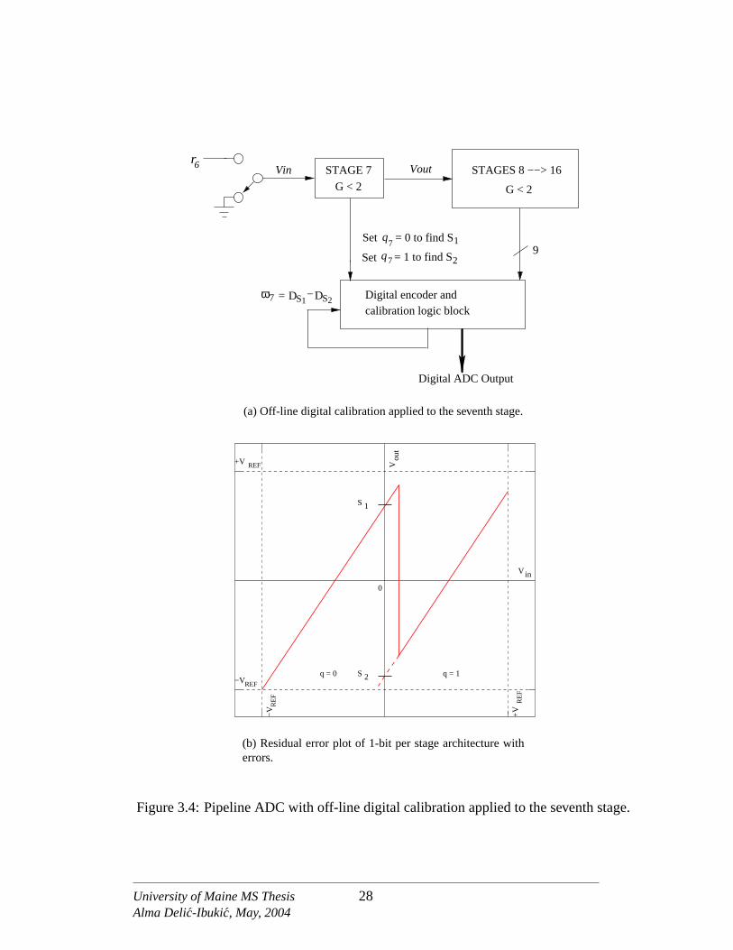
Figure3.4 illustrates the calibration process for a single stage of the ADC. The
illustrated case is based on the implementation of a 14-bit ADC with 16 identical stages,
interstage gains less than two, and 1-bit per stage topology. Gains less than two are
chosen for all 16 stages so the output of each stage does not saturate the remaining
stages. Calibration begins with the least significant stages (the end of the pipeline)
and progresses toward the most significant stages. For example, to calibrate stage 7,
we must assume that stages 8-16 have already been calibrated, or have been fabricated
to sufficient accuracy that calibration is not needed. Figure3.4(a)shows the off-line
digital calibration applied to the seventh stage of a 16-stage architecture. Figure3.4(b)
shows residual characteristics for the stage being calibrated. Following calibration of
the seventh stage, the process continues with the sixth stage, and so on until the first
stage is reached and the calibration of the converter is complete.
In Chapter2, the equation for the digital output of the converter was derived. For
theN -stage converter the digital output had the following form:
D = q1 (G1G2G3 . . . GN−1) + q2 (G2G3G4 . . . GN−1) + q3 (G3G4G5 . . . GN−1)
+ . . . qN−2 (GN−2GN−1) + qN−1GN−1 + qN (3.4)
Each stage output bit is given a weight indicated by the gain products given in paren-
thesis. Most pipeline ADCs use ‘nominal’ design gains to construct the digital output.
This approach is correct only if the converter is free of any gain or sub-DAC errors. If
the implemented gain is different from the design value, or if sub-DAC errors exist, there
University of Maine MS ThesisAlma Delic-Ibukic, May, 2004
27
DS2ω 7
q7 = 0 to find S1
= 1 to find Sq7 2
STAGES 8 −−> 16
G < 2
STAGE 7
G < 2
VoutVin6r
9
−DS1=
Set
Set
Digital encoder andcalibration logic block
Digital ADC Output
(a) Off-line digital calibration applied to the seventh stage.
Vin
Vou
t
+V REF
−VREF
−V
RE
F
+V
RE
F
S 1
S 2q = 0 q = 1
0
(b) Residual error plot of 1-bit per stage architecture witherrors.
Figure 3.4: Pipeline ADC with off-line digital calibration applied to the seventh stage.
University of Maine MS ThesisAlma Delic-Ibukic, May, 2004
28
will be error in the ADC output. Making these weights programmable is the idea behind
most of the digital calibration techniques. This is the case for the calibration algorithm
derived by Karanicolaset al., where the correction termsωi are programmable and are
updated each time a stage is being calibrated. The converter output equation3.4can be
re-written in terms of these weights,
D =N∑
i=1
qiωi, (3.5)
whereqi is the output bit for stagei andN is the number of stages used.
Pipeline error characteristics often show discontinuities associated with the change
in the output of the sub-ADC comparators. The residual error shown in Figure3.4(b)
consists of two segments (forq=0 andq=1) and the transition between the segments is
determined by the comparator threshold. The goal of digital calibration is to make sure
that for the same input voltage, the digital ADC output remains unchanged regardless
of which segment is selected by the sub-ADC comparator of the stage. To assure this
consistency, the converter output is examined for a stage input set to zero volts, where
the stage is forced to operate on each of the segments. Settingq7=0 with Vin=0, forces
Stage 7 to operate on the left segment, producing output residual voltageS1. S1 is
quantized by the remaining pipeline stages (stages 8, 9, 10,..., 16), producing digital
outputDS1. When Stage 7 is added to the pipeline, the resulting digital output is given
by
q7ω7 + DS1 = DS1 (3.6)
Settingq7=1 (Vin=0) forces Stage 7 to operate on the right segment, producing residual
voltageS2. S2 is quantized by the remaining pipeline stages to give a digital outputDS2 .
The pipeline output in this case is
q7ω7 + DS2 = ω7 + DS2 (3.7)
University of Maine MS ThesisAlma Delic-Ibukic, May, 2004
29

For a consistent digital output,ω7 should be selected so (3.6) and (3.7) agree. Setting
(3.6) and (3.7) equal to each other gives the expression forω7.
ω7 = DS1 −DS2 (3.8)
The residual voltage termsS1 andS2 for a single stage are identified in Figure
3.4(b). Once the digital representationsDS1 andDS2 for the residual voltagesS1 andS2
are found, the correction termωi can be obtained. The correction termωi is fed back to
the digital encoder and calibration logic block. This value is a weight associated with
the bit of the stage being calibrated and it carries the information about the interstage
gain and sub-DAC errors.
The digital calibration scheme discussed above requires two constants per stage,
DS1 andDS2 . The difference between these constants,ωi, needs to be stored in memory
to be used during the normal operation of the converter. The technique can be extended
to work on multi-bit per stage architectures. Longer calibration times would be required
for multiple calibration terms to be calculated and stored in memory. For every calibrated
stage, each comparator threshold requires an additionalωi term. Figure3.5 shows
a residual plot for 1.5-bits per stage pipeline architecture. There are two different
comparator threshold voltages and therefore, four measurements (DS1 , DS2 , DS3 and
DS4) are required to calibrate a stage. This requires two subtractions and two correction
termsωi per stage.
3.4.2 Simulation Results
A 14-bit ADC using 1-bit per stage architecture and digital self-calibration algorithm
discussed previously is simulated in MATLAB. Sixteen identical stages are implemented
to account for a reduced interstage gain and still maintain 14 bits of resolution. The gain,
University of Maine MS ThesisAlma Delic-Ibukic, May, 2004
30

−V
RE
F
+V
RE
F
−VREF
+VREF
q = 0 q = 1 q = 2
Vou
t
Vin
S1
S2
S3
S4
Figure 3.5: Residual plot for 1.5-bits per stage pipeline architecture.
threshold and sub-DAC reference voltages of each stage can be controlled indepen-
dently. This enables error mechanisms to be introduced in the pipeline and their effects
monitored in a converter output. Gains of a stage are reduced enough so the residual is
contained within the reference boundary of the next stage. This gain reduction takes care
of the comparator offset errors. Nominal gain for all 16 stages was set to 1.81 (Section
2.3). The input range (VFS) for this converter was set to+−1.12 V, giving an ideal quanti-
zation interval ofQ = 2(1.12)214 = 0.137 mV. The reference voltage for the converter was
set toVREF = 1 V.
Figure3.6shows the output spectrum of an ideal simulated 14-bit converter. In
all 16 stages, values for gain, threshold and sub-DAC reference voltages were kept ideal.
The sampling rate was set to 51.2 MHz with the sinusoidal input signal at 1 MHz. The
signal amplitude was at -1 dBFS (994 mV) and additive white Gaussian dither with
variance1.3(Q2/12) was added to the input signal.
University of Maine MS ThesisAlma Delic-Ibukic, May, 2004
31

0 5 10 15 20 25
−120
−100
−80
−60
−40
−20
0
Frequency (MHz)
AD
C O
utpu
t Spe
ctru
m (
dBF
S)
1
2 3 4
5
6 7 8
9
10
11
12
14 15
16
17
18
19
20
21 22 23
24 25
26
27 28
29 30
31 32
33 34 35
36 38 39 40 42
44
45
46
47 48
49
50
SFDR = 100.7002 dB
SNRD = 81.5851 dB
ENOB = 13.26 bits
Figure 3.6: Simulated 14-bit pipeline (ideal) ADC withFin = 1 MHz.
University of Maine MS ThesisAlma Delic-Ibukic, May, 2004
32

The digital self-calibration algorithm derived by Karanicolaset al. [4] is imple-
mented only on the first seven stages of the simulated pipeline ADC. Stages 8 though
16 are assumed to be adequate for measuring the error for Stage 7 without the need
for calibration. These nine stages must be capable of measuring the Stage 7 residual
voltage with an accuracy of 8 bits, well within the technology limitations of current
pipeline converters [14]. Pipeline converter performance is typically determined by the
errors introduced in the first few stages.
Figure3.7shows the simulated residual error characteristics for the ideal, calibrated
and uncalibrated 14-bit converter. All stages are kept ideal, with the only noise contri-
bution coming from the additive white Gaussian dither signal. Calibration is imple-
mented in the foreground and obtained values are then used to form the ADC output
code during the normal converter operation. The sampling rate was set to 51.2 MHz
with the input signal at 150 KHz and amplitude at -1 dBFS. The residual error is found
by removing the DC value and fundamental component of the input signal from the
output sample sequence. This error determines signal to noise distortion ratio (SNDR)
and therefore, the effective number of bits (ENOB) for the converter. The residual error
for the uncalibrated ideal converter is within+−1.5 LSBs and for the calibrated ideal
converter this range is+−2 LSBs. The small discrepancy in the residual error range
for uncalibrated and calibrated ideal converter is caused by the accuracy with which
the measurement of the correction terms,ωi, required for the digital calibration can
be conducted. Even with the small difference in the residual error range, the calibrated
converter virtually achieves the resolution of the ideal (uncalibrated) converter. In reality,
a converter with the ideal stages does not exist. Using calibrated values to form the
output code of the converter generally gives more accuracy than using the nominal
converter values.
Dominant errors for pipeline ADCs include sub-DAC and gain errors. Both
of these errors depend on the accuracy of the capacitor matching and charge injection
University of Maine MS ThesisAlma Delic-Ibukic, May, 2004
33

0 100 200 300 400 500 600 700 800 900 1000−2
−1.5
−1
−0.5
0
0.5
1
1.5
2
SFDR = 88.2681 dB
ENOB = 12.7532 bits
SFDR = 100.0762 dB
ENOB = 13.2471 bits
Sample Number
Res
idua
l Err
or (
LSB
)
uncalibratedcalibrated
Figure 3.7: Calibrated vs. uncalibrated residual error for a simulated pipeline (ideal)ADC.
University of Maine MS ThesisAlma Delic-Ibukic, May, 2004
34

effects. To demonstrate performance of the digital self-calibration algorithm, errors
were introduced in gain, threshold and reference voltages of the first seven stages. Gain
and reference voltage error contributions were based on the capacitor matching capabil-
ities in current CMOS process technologies [14]. Capacitor matching error between
0.1- 0.5% was simulated. For threshold voltage variations, error of up to 10% of VFS
was simulated. This is the maximum error allowed for the chosen gain. Table3.1
lists parameters and errors associated with them for the first seven stages used in the
simulation. Ideal values are also shown. The definition of these parameters for a given
stage is illustrated in Figure3.8. Sub-DAC error is controlled by the reference voltage
locations,VDAC1 andVDAC2, and sub-ADC error is controlled by the threshold voltage
location,VADC .
Figures3.9 and3.10show the output spectrum of the simulated 14-bit pipeline
ADC with and without calibration applied. Errors from Table3.1 were introduced
at different pipeline locations to show their impact on the converter output and effec-
tiveness of the calibration algorithm. The sampling rate was set to 51.2 MHz. The test
signal was set to 1 MHz with the amplitude at -1 dBFS. The input range of the converter
was+−1.12 V. Plots provide a visual representation of how much distortion is introduced
by the first three stages compared when all seven stages are error contributors.
Simulation results confirm that the dominant errors are those introduced at the
front end of the pipeline. The first few stages of the pipeline determine the final converter
resolution. Calibrating the first seven stages is adequate to correct for the dominant error
sources of the pipeline converter and obtain a full converter resolution. The simulations
also demonstrate that the digital self-calibration algorithm derived by Karanicolaset al.
[4] is successful in correcting for the errors introduced at any location of the pipeline.
Once the errors were introduced into the pipeline, the uncalibrated converter resolution
dropped to 10 effective bits, while the calibrated converter maintained 13 effective bits
of resolution.
University of Maine MS ThesisAlma Delic-Ibukic, May, 2004
35

VDAC1 VDAC2 VADC GainIdeal -0.5000 0.5000 0.00 1.810stage-1 -0.5005 0.5015 0.02 1.804stage-2 -0.4975 0.5005 -0.04 1.819stage-3 -0.4985 0.5025 0.05 1.812stage-4 -0.5025 0.4995 -0.09 1.808stage-5 -0.5010 0.4975 0.10 1.801stage-6 -0.4995 0.4985 -0.05 1.806stage-7 -0.5015 0.5010 0.03 1.817
Table 3.1: Parameters for simulated 14-bit Pipeline ADC (units in volts).
−VREF +VREF
VDAC1VDAC2
V ADC
Sub−DAC Output Voltages
Vou
t
Vin
0
Sub−ADC Threshold Voltage
gain = slope
Figure 3.8: Locations of parameters for simulated ADC.
University of Maine MS ThesisAlma Delic-Ibukic, May, 2004
36

0 5 10 15 20 25
−120
−100
−80
−60
−40
−20
0
Frequency (MHz)
AD
C O
utpu
t Spe
ctru
m (
dBF
S)
1
2
3
4
5
6
7
8
9
10
11
12
13
14
15
16
17
18 19
20 21
22 23
24 25
26 27
28 29
30 31
32 33 34 35 36 37 38 39 40 41 42
43 44 45 46 47 48 49
50
SFDR = 71.0149 dBSNRD = 67.588 dBENOB = 10.9349 bits
1
2 3
4
5
6
7
8
9
10
11
12
13 15
16 17
19
20
21 23
24
25 27
28
29
31 32
34
35 36
37
38
39
40
41 42 43
45
46 47
48 49 50
SFDR = 86.3906 dBSNRD = 78.7199 dBENOB = 12.784 bits
(a) Output spectrum with errors in first stage only.
0 5 10 15 20 25
−120
−100
−80
−60
−40
−20
0
Frequency (MHz)
AD
C O
utpu
t Spe
ctru
m (
dBF
S)
1
2
3
4 5 6 7
8
9
10
11
12
13
14
15 16
17
18
19
20 21
22
23
24
25
26
27 28
29
30
31
32 33
34
35
36
37
38
39 40
41
42
43
44
45
46
47 48
49
50
SFDR = 67.4369 dBSNRD = 63.226 dBENOB = 10.2103 bits
1
2 3 4
5
6
7
9
10
11
12
13
14
15
16 17 18
19
20
21
22
23 25
26 27
28
29
30 31 32 33 34 35 36
37 39
40 41
42
43
44
45
46 47 48
50
SFDR = 86.0854 dBSNRD = 78.3154 dBENOB = 12.7168 bits
(b) Output spectrum with errors in first and second stage only.
Figure 3.9: Simulated ADC output spectrum with (red) and without (blue) digital self-calibration applied.
University of Maine MS ThesisAlma Delic-Ibukic, May, 2004
37

0 5 10 15 20 25
−120
−100
−80
−60
−40
−20
0
Frequency (MHz)
AD
C O
utpu
t Spe
ctru
m (
dBF
S)
1
2
3
4
5 6
7 8 9
10
11
12
13
14
15 16
17
18 19 20 21
22
23
24
25
26
27 28
29
30
31
32 33
34
35
36
37
38
39
40 41
42
43
44
45
46 47 48
49 50
SFDR = 68.8061 dBSNRD = 64.4165 dBENOB = 10.4081 bits
1
2
3
4
5
6
7
8
9
10
11
12
13
14
15
16
17
18
19
20
21
22
23
24
25
26
27 28
29
30 31 33
34 35 36 37 38 39 40
41 42 43 44
45
46
47 48 49
50
SFDR = 83.8051 dBSNRD = 77.8129 dBENOB = 12.6334 bits
(a) Output spectrum with errors in first, second and third stage only.
0 5 10 15 20 25
−120
−100
−80
−60
−40
−20
0
Frequency (MHz)
AD
C O
utpu
t Spe
ctru
m (
dBF
S)
1
2
3
4
5
6 7 8
9
10
11
12
13
14
15 16
17
18
19
20 21
22
23
24 25
26
27 28
29
30
31
32 33
34
35
36 37 38
39 40
41 42 43
44 45
46
47 48 49 50
SFDR = 70.6884 dBSNRD = 65.4189 dBENOB = 10.5746 bits
1
2 3
4
5
7 8 9
10 11 13 14 15
16 17
19
20 21
22 23
24
25 26
27
28
29 30
31 32
33 34 35 36
37 38 39 40
41
42 43 44 45
46 47 48
49
50
SFDR = 89.6938 dBSNRD = 79.9231 dBENOB = 12.9839 bits
(b) Output spectrum with errors in first seven stages only.
Figure 3.10: Simulated ADC output spectrum with (red) and without (blue) digital self-calibration appliedcont..
University of Maine MS ThesisAlma Delic-Ibukic, May, 2004
38

Chapter4 describes a novel real-time digital calibration technique implemented
in Verilog HDL. The calibration technique is based on the algorithm derived in [4]. A
lower test frequency facilitates the comparison between Verilog HDL and MATLAB
simulations. Gain, sub-DAC and sub-ADC block errors are static errors. They do not
depend on the dynamic nature of the input signal because these errors occur after the
sample is captured by the S/H block. While a change in test frequency will affect
distortion introduced by S/H block, it will not affect performance of the calibration
algorithm introduced here.
Figures3.11, 3.12, 3.13, and 3.14 show residual error characteristics for the
simulated 14-bit calibrated and uncalibrated ADC. Again, the sampling frequency of
51.2 MHz was used. The sinusoidal test signal was reduced to 150 KHz with the
amplitude at -1 dBFS. This frequency corresponds to three sine wave cycles in a block
of 1024 ADC output samples. Errors, tabulated in Table3.1, are introduced at different
stages of the converter. Figures3.11(a)and3.11(b)show the residual error character-
istics when errors are introduced only in a first stage of the pipeline. Degradation of the
converter’s performance due to the first stage errors is the same as degradation observed
in the output spectrum plot of Figure3.9(a). This shows independence of gain, sub-
DAC and sub-ADC errors on the input frequency. Also, Figures3.11, 3.12, 3.13, and
3.14show that when calibration is implemented, the residual error stays within+−2 LSBs.
This shows the advantage of having a digital calibration algorithm as a regular addition
to a pipeline ADC design.
3.5 Real-Time Digital Calibration Scheme Development
The foreground digital calibration algorithm developed by Karanicolaset at.[4]
can be extended to work in real-time and this novel digital calibration approach is
discussed here.
University of Maine MS ThesisAlma Delic-Ibukic, May, 2004
39

0 2000 4000 6000 8000 10000 12000 14000 16000−10
−8
−6
−4
−2
0
2
4
6
8
10
SFDR = 86.0046 dBENOB = 12.7167 bits
SFDR = 71.1154 dBENOB = 10.917 bits
Output Code
Res
idua
l Err
or (
LSB
)
uncalibratedcalibrated
(a) Residual error vs. the output code with first stage error contributions.
0 100 200 300 400 500 600 700 800 900 1000−10
−8
−6
−4
−2
0
2
4
6
8
10
SFDR = 86.0046 dBENOB = 12.7167 bits
SFDR = 71.1154 dBENOB = 10.917 bits
Sample Number
Res
idua
l Err
or (
LSB
)
uncalibratedcalibrated
(b) Residual error characteristics with first stage error contributions.
Figure 3.11: Simulated ADC residual error characteristics with (red) and without (blue)digital self-calibration applied. Errors introduced in a first stage.
University of Maine MS ThesisAlma Delic-Ibukic, May, 2004
40

0 2000 4000 6000 8000 10000 12000 14000 16000−10
−8
−6
−4
−2
0
2
4
6
8
10SFDR = 87.1853 dBENOB = 12.7134 bits
SFDR = 67.5494 dBENOB = 10.2068 bits
Output Code
Res
idua
l Err
or (
LSB
)
uncalibratedcalibrated
(a) Residual error vs. the output code with error contributions from the first two stages.
0 100 200 300 400 500 600 700 800 900 1000−10
−8
−6
−4
−2
0
2
4
6
8
10SFDR = 87.1853 dBENOB = 12.7134 bits
SFDR = 67.5494 dBENOB = 10.2068 bits
Sample Number
Res
idua
l Err
or (
LSB
)
uncalibratedcalibrated
(b) Residual error characteristics with error contributions from the first two stages.
Figure 3.12: Simulated ADC residual error characteristics with (red) and without (blue)digital self-calibration applied. Errors introduced in a first two stages.
University of Maine MS ThesisAlma Delic-Ibukic, May, 2004
41

0 2000 4000 6000 8000 10000 12000 14000 16000−10
−8
−6
−4
−2
0
2
4
6
8
10SFDR = 83.5721 dBENOB = 12.6261 bits
SFDR = 69.0099 dBENOB = 10.4039 bits
Output Code
Res
idua
l Err
or (
LSB
)
uncalibratedcalibrated
(a) Residual error vs. the output code with error contributions from the first threestages.
0 100 200 300 400 500 600 700 800 900 1000−10
−8
−6
−4
−2
0
2
4
6
8
10SFDR = 83.5721 dBENOB = 12.6261 bits
SFDR = 69.0099 dBENOB = 10.4039 bits
Sample Number
Res
idua
l Err
or (
LSB
)
uncalibratedcalibrated
(b) Residual error characteristics with error contributions from the first three stages.
Figure 3.13: Simulated ADC residual error characteristics with (red) and without (blue)digital self-calibration applied. Errors introduced in a first three stages.
University of Maine MS ThesisAlma Delic-Ibukic, May, 2004
42

0 2000 4000 6000 8000 10000 12000 14000 16000−10
−8
−6
−4
−2
0
2
4
6
8
10SFDR = 90.5548 dBENOB = 13.0055 bits
SFDR = 70.6735 dBENOB = 10.5541 bits
Output Code
Res
idua
l Err
or (
LSB
)
uncalibratedcalibrated
(a) Residual error vs. the output code with error contributions from the first sevenstages.
0 100 200 300 400 500 600 700 800 900 1000−10
−8
−6
−4
−2
0
2
4
6
8
10SFDR = 90.5548 dBENOB = 13.0055 bits
SFDR = 70.6735 dBENOB = 10.5541 bits
Sample Number
Res
idua
l Err
or (
LSB
)
uncalibratedcalibrated
(b) Residual error characteristics with error error contributions from the first sevenstages.
Figure 3.14: Simulated ADC residual error characteristics with (red) and without (blue)digital self-calibration applied. Errors introduced in a first seven stages.
University of Maine MS ThesisAlma Delic-Ibukic, May, 2004
43

1φ
2φ
Figure 3.15: Example of a two-phase, non-overlapping clock signal used in pipelineADC architecture.
The algorithm derived by Karanicolaset al. [4] is attractive because no multi-
plication is required to obtain calibration values. The algorithm corrects for major
static errors of a pipeline ADC. These errors include all errors illustrated in Figure3.1:
comparator offset, charge injection and capacitor mismatch errors.
Pipeline architecture ADCs rely on a two-phase, non-overlapping clock signal.
Figure3.15 shows an example of a non-overlapping clock signal. All the odd stages
in a pipeline sample during phaseφ1 and present the valid residue output to the next
stage duringφ2. All the even stages work on the opposite clock phase. This allows for
all stages in the pipeline to operate concurrently. A novel real-time digital calibration
based on the algorithm derived by Karanicolaset al. [4] was realized using two extra
stages located at the end of the pipeline. These two extra stages are active only during
calibration. As seen in Sections3.1 and3.4, the error contribution from the first few
pipeline stages dominate the final converter performance. Therefore, adding an extra
two stages at the end of the pipeline will not degrade performance of the converter. Two
extra stages at the end of the pipeline allow for a calibration sample to be introduced in
the pipeline and still maintain the normal operation of the converter. Table3.2 shows
propagation of samples through the pipeline during the calibration process. Table3.2
is based on a 14-bit ADC with 1-bit per stage topology, 16 identical stages plus two
University of Maine MS ThesisAlma Delic-Ibukic, May, 2004
44

additional stages for calibration (total of 18 pipeline stages), and gains less than two.
Numbers 1 through 18 indicate pipeline stages. Two-phase, non-overlapping clocks
are indicated byφ1 andφ2. Values -1, 0, 1, 2, ..., correspond to sample number being
acquired by a given stage, andD−1, D0, D1, D2, ..., correspond to digital representation
of the sample produced at the output of a given stage. For example, sample number 4 is
processed by Stage 1 on a phaseφ1 and its digital representation as well as a residual is
available onφ2. At this time, Stage 2 is ready to acquire this residual voltage. Stage 2
produced its coarse digital representation on the followingφ1. This goes on until all 16
stages in a pipeline have coarse digital representation of sample number 4 available for
the digital encoder and calibration logic block where the corresponding digital value for
the sample is obtained.
After the inherent pipeline delay, digital outputs become available on everyφ1.
This is considered a normal converter operation and it must be preserved during the
calibration process. When calibrating a stage using the digital calibration algorithm
derived in [4], the stage being calibrated needs to be taken off line which in turn will
interrupt normal operation of the converter. To avoid this, two extra stages are added
at the end of the pipeline. This allows one conversion cycle to be freed for calibration
purposes and at the same time maintain normal converter operation.
When calibrating, all samples at the various stages of the pipeline are shifted by
two stages down in the pipeline. The two extra stages at the end of the pipeline make
sure the converter maintains a full 14-bit output during the calibration cycle. Table3.2
shows the calibration of Stage 5. An artificial sample is introduced at the beginning of
the pipeline denoted “T”. At the same moment, sample number 3 is shifted as an input
into Stage 3. This means that Stage 3 for this instant acts as a first stage of the pipeline
and last stage for this sample will be Stage 18. Sample number 2, which should be at
the calibration moment occupying Stage 3, is now shifted two stages down to the next
free odd stage, Stage 5. Sample number 1, which should be occupying Stage 5 is shifted
University of Maine MS ThesisAlma Delic-Ibukic, May, 2004
45

Increasingtim
e−→
Stage
φ1
φ2
φ1
φ2
φ1
φ2
φ1
φ2
φ1
φ2
φ1
φ2
φ1
φ2
φ1
φ2
φ1
φ2
φ1
φ2
φ1
φ2
φ1
φ2
φ1
11
D1
2D
2T
DT
4D
45
D5
...
2D
01
D1
2D
2T
DT
4D
45
D5
...
30
D0
1D
13
D3
TD
T4
D4
5D
5...
4D−
10
D0
1D
13
D3
TD
T4
D4
5D
5...
5-1
D−
10
D0
2D
23
D3
C5
DC
54
D4
5D
5...
6-1
D−
10
D0
2D
23
D3
C5
DC
54
D4
5D
5...
7-1
D−
11
D1
2D
23
D3
C5
DC
54
D4
5D
5...
8-1
D−
11
D1
2D
23
D3
C5
DC
54
D4
5D
5...
90
D0
1D
12
D2
3D
3C
5D
C5
4D
45
D5
...
100
D0
1D
12
D2
3D
3C
5D
C5
4D
45
D5
...
11-1
D−
10
D0
1D
12
D2
3D
3C
5D
C5
4D
45
D5
...
12-1
D−
10
D0
1D
12
D2
3D
3C
5D
C5
4D
45
D5
...
13-1
D−
10
D0
1D
12
D2
3D
3C
5D
C5
4D
45
D5
...
14-1
D−
10
D0
1D
12
D2
3D
3C
5D
C5
4D
45
D5
...
15-1
D−
10
D0
1D
12
D2
3D
3C
5D
C5
4D
45
D5
16-1
D−
10
D0
1D
12
D2
3D
3C
5D
C5
4D
45
D5
17-1
D−
10
D0
1D
12
D2
3D
3
18-1
D−
10
D0
1D
12
D2
3D
3
Table3.2:
Sam
plepropagation
throughthe
pipelinefor
theproposed
real-time
digitalcalibrationtechnique.
University of Maine MS ThesisAlma Delic-Ibukic, May, 2004
46

to the next odd stage, Stage 7. The last sample that needs to be shifted at the calibration
instant is located in Stage 14. Instead of going to Stage 15 on the next clock phase, it
will be routed to Stage 17. The same shift is used for the coarse digital outputs for these
samples. The only difference is the clock phase on which shift of the digital counterpart
occurs. It can be seen from Table3.2 that all samples still propagate through 16 stages
with no time delay introduced and no lost samples. Also, Stage 5 can be calibrated as
described in Section3.4.
Due to the pipeline shift, certain considerations need to be taken into account
when forming the digital output code during the calibration process. Equation3.4
shows formation of the digital output for theN -stage, 1-bit per stage converter. With all
identical stages (3.4) becomes
D = q1GN−1 + q2G
N−2 + q3GN−3 + . . . qN−2G
2 + qN−1G + qN (3.9)
From (3.9) it can be seen that there is a weight associated with each bit of the stage.
When calibration occurs, Stage 3 becomes the first stage of the pipeline, and should be
given weightGN−1. Similarly the weights associated with the other stages need to shift
to reflect the reorganization of the pipeline. The weights for Stages 1, 2, 3, ..., need to
be available at location of Stages 3, 4, 5, ..., respectively for the correct formation of the
final digital output during the calibration.
Figure3.16shows the proposed continuous time digital calibration architecture
for an 8-stage, 1-bit per stage pipeline converter. Stages 9 and 10 are active only during
the calibration process. In the figure, only stages 1 through 4 are calibrated, and stages
5 through 8 are assumed to be fabricated with sufficient accuracy. Each “calibration
logic” block has two weights associated with the given stage. One set of weights is used
only during the calibration process and reflect the reorganization of the pipeline during
calibration instant. The other set of weights goes with the normal converter operation.
University of Maine MS ThesisAlma Delic-Ibukic, May, 2004
47

STA
GE
10ST
AG
E 1
STA
GE
5ST
AG
E 4
STA
GE
9ST
AG
E 3
STA
GE
2ST
AG
E 7
STA
GE
6
cal. logic
cal. logic
cal. logic
cal. logic
cal. logic
cal. logic
cal. logic
cal. logic
cal. logic
cal. logic
q4q6
q8q10
GG
1
STA
GE
8V
in
GG
//
G/
G
q1q
q2
3q5
q7q9
G
2G
G
/4
G
GG G
GG
G
10
2 03 1
245 3
6
4
7
53
67
ωω
ωω
Figure
3.16:P
roposedreal-tim
edigitalcalibration
architecture.
University of Maine MS ThesisAlma Delic-Ibukic, May, 2004
48

In the case of the first four stages, these weights are programmable and their corrected
versionωi is obtained during calibration. Programmable weights are labeledωi, wherei
corresponds to stage numbers 1 through 4. Discussion of implementation and simulation
results of a continuous digital calibration technique follow in Chapter4.
University of Maine MS ThesisAlma Delic-Ibukic, May, 2004
49

CHAPTER 4
Implementation of a Continuous Digital Calibration Scheme in
Verilog HDL
This chapter will discuss the implementation of the digital calibration algorithm
in real-time using Verilog HDL. A state machine that controls the calibration procedure
and modifications of the error correction logic is discussed. A 14-bit pipeline ADC
implemented using 16 identical stages and 1-bit per stage topology is used for verifi-
cation of the developed calibration technique. Also, the complexity of the design is
evaluated.
4.1 Digital Calibration in Verilog HDL
Verilog Hardware Description Language (HDL) is a software programming language
used to model the intended operation of a piece of digital hardware [22]. Verilog HDL
is a widely used tool when designing circuits that perform a specific sequence of opera-
tions. The continuous digital calibration scheme developed in Chapter3 relies on the
sequence of the events to be executed in predetermined manner. This section discusses
digital logic necessary for realization of the continuous digital calibration technique.
4.1.1 Finite State Machine (FSM) Description
Finite State Machines (FSMs) have shown to be very efficient in modeling sequential
circuits [22]. This section describes a FSM implementation of the real-time calibration
procedure.
The designed state machine controls the calibration process of each stage, the
predetermined data path shift which occurs during calibration, activation of the extra
two stages at the end of the pipeline, and writing of the correctedω value back to the
University of Maine MS ThesisAlma Delic-Ibukic, May, 2004
50

pipeline stage being calibrated. The state machine was designed using a “slave” state
machine which is controlled by a “master” state machine. Figure4.1shows a simplified
flow chart of the sequence of the events to be performed by the master state machine.
Two passes per stage are necessary to determine the correction termω for that stage. The
variable ‘counter’ is used to determine if the two necessary values (digital representa-
tions ofS1 andS2) are obtained for the stage being calibrated. Section3.4described the
digital calibration algorithm implemented here and Figure3.4(b)showed the location of
measured termsS1 andS2. The variable ‘Stage’ is used to keep track of the stage being
calibrated. The actual calibration of the stage is controlled by the slave state machine,
indicated by the ‘CALIBRATED’ keyword.
The state machine was designed for a 14-bit pipeline ADC implemented using
16 identical stages with gains less than two and 1-bit per stage topology. Two extra
stages are added at the end of the pipeline for a continuous time calibration purposes.
This makes a total of 18 identical pipeline stages. Only the first seven stages are being
calibrated and have programmable weights associated with the stage. Details on the
implemented converter were given in Section3.4. The state machine is clocked using
one of the non-overlapping clocks,φ1. Any given signal from the FSM will stay ‘high’
for the entire clock period ofφ1. Two non-overlapping clocks are used to operate a
pipeline ADC. During a ‘low’ time ofφ1, the second clock signalφ2 will be active and
therefore, the necessary changes within the even stages can be made.
As mentioned before, the FSM controls the sequence of the events essential
for the continuous calibration scheme to succeed. On the converter power up, and
before ‘Calibration’ signal occurs, the ‘Reset’ signal must be asserted. Once the ‘Reset’
signal occurs, nineteen clock cycles are necessary to initialize the weights of all eighteen
pipeline stages. Each stage is initialized in turn with two weights used for the digital
correction. One set of weights is associated with the normal operation of the converter,
and a second set of shifted weights is required for the (re)calibration process (Section
University of Maine MS ThesisAlma Delic-Ibukic, May, 2004
51

INITIALIZE:
counter = 0;Stage = 7;
NOif
= 1Start Calibration
YES
NOifcounter = 2
counter = 0;
Stage = Stage − 1;
if
Stage = 0NOYES
counter = counter + 1;
CALIBRATE Stage;
RESET = 1if NO
YES
Write two sets of weights for each stage.These are used in forming the digital output code.
YES
(slave FSM)
Figure 4.1: Simplified description of the sequence of events implemented by the masterFinite State Machine (FSM).
University of Maine MS ThesisAlma Delic-Ibukic, May, 2004
52

3.5). Table4.1 shows the 19-bit binary and the corresponding decimal values for the
two sets of weights associated with each pipeline stage. MATLAB simulations were
used to verify that 19-bit representations of weights were adequate to form 14-bit ADC
outputs. Note that the weights used during normal converter operation for the first seven
stages in the pipeline are programmable, and are indicated by the red color. They can be
replaced once the correction terms are obtained during the calibration procedure.
At any instant (after the nineteen clock cycles has passed), the ‘Calibration’
signal can occur. The master FSM controls the calibration sequence of stages being
calibrated. The calibration process is conducted starting with the last stage in the
pipeline being calibrated and moving toward the front of the pipeline. A slave FSM
counts clock cycles needed to start the calibration of a given stage and controls the
timing associated with the capture of the digital representation of theS1 andS2 terms.
For example, Table3.2shows sample propagation through the pipeline when Stage 5 is
being calibrated. Once the calibration is initiated and it is time to calibrate Stage 5, two
clock cycles ofφ1 need to occur before the calibration of Stage 5 can start. Calibration
of Stage 5 starts on the third clock cycle ofφ1 and six clock cycles later the digital repre-
sentations ofS1 andS2 are available for Stage 5. Also, at this instant, Stage 18 has the
digital representation of the current sample available for the output and therefore, the
normal operation of the converter is never interrupted.
The state machine uses a clock counter to control the timing of all calibration
steps. To obtain a digital representation ofS1 or S2 for a single stage, nine clock cycles
are required. The designed slave state machine uses 11 clock cycles. This allows for
the correction term to be calculated and written back to the calibrated stage. Therefore,
to obtain a correction term,ω, for a single stage, 22 clock cycles are necessary. The
calculated weight,ω, is the difference between the digital representations ofS1 andS2.
To calibrate 7 stages a total of 154 clock cycles are needed. The sampling rate for the
University of Maine MS ThesisAlma Delic-Ibukic, May, 2004
53
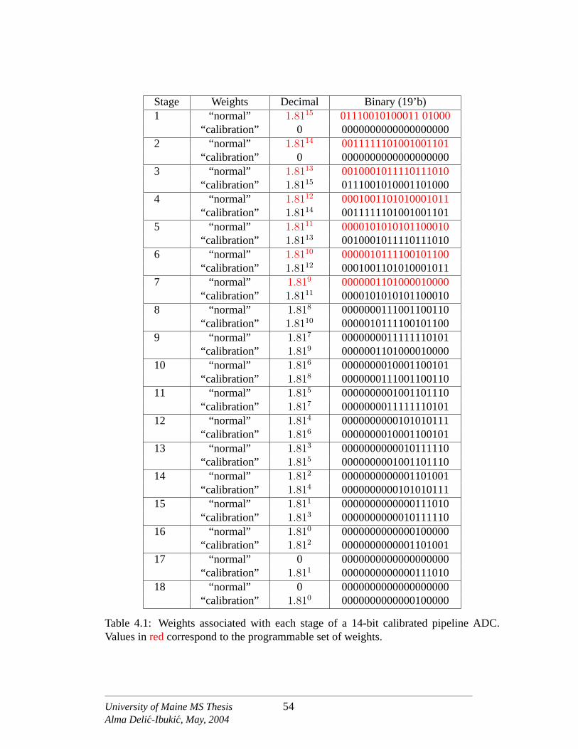
Stage Weights Decimal Binary (19’b)1 “normal” 1.8115 01110010100011 01000
“calibration” 0 00000000000000000002 “normal” 1.8114 0011111101001001101
“calibration” 0 00000000000000000003 “normal” 1.8113 0010001011110111010
“calibration” 1.8115 01110010100011010004 “normal” 1.8112 0001001101010001011
“calibration” 1.8114 00111111010010011015 “normal” 1.8111 0000101010101100010
“calibration” 1.8113 00100010111101110106 “normal” 1.8110 0000010111100101100
“calibration” 1.8112 00010011010100010117 “normal” 1.819 0000001101000010000
“calibration” 1.8111 00001010101011000108 “normal” 1.818 0000000111001100110
“calibration” 1.8110 00000101111001011009 “normal” 1.817 0000000011111110101
“calibration” 1.819 000000110100001000010 “normal” 1.816 0000000010001100101
“calibration” 1.818 000000011100110011011 “normal” 1.815 0000000001001101110
“calibration” 1.817 000000001111111010112 “normal” 1.814 0000000000101010111
“calibration” 1.816 000000001000110010113 “normal” 1.813 0000000000010111110
“calibration” 1.815 000000000100110111014 “normal” 1.812 0000000000001101001
“calibration” 1.814 000000000010101011115 “normal” 1.811 0000000000000111010
“calibration” 1.813 000000000001011111016 “normal” 1.810 0000000000000100000
“calibration” 1.812 000000000000110100117 “normal” 0 0000000000000000000
“calibration” 1.811 000000000000011101018 “normal” 0 0000000000000000000
“calibration” 1.810 0000000000000100000
Table 4.1: Weights associated with each stage of a 14-bit calibrated pipeline ADC.Values inredcorrespond to the programmable set of weights.
University of Maine MS ThesisAlma Delic-Ibukic, May, 2004
54

converter implemented is 51.2 MHz. At this speed, the converter requires a total time of
3 µs to complete a calibration of 7 stages.
In addition to monitoring the calibration status of a stage, the clock counter is
responsible for setting and resetting different calibration lines for each stage. Calibration
lines have functions such as forcing the input to a sub-DAC to 0 or 1 when a stage is
being calibrated, changing the input data path, activating the extra two stages at the
end of the pipeline, monitoring the correct digital output collection sequence during
calibration period and writing the corrected term after calibration back to the calibrated
stage. Once all 7 stages have been calibrated the state machine is idle until the next
calibration signal is initiated.
4.1.2 Required Stage Modifications
Pipeline stages need to be modified for the FSM to be able to make adjust-
ments to a stage while calibrating. All odd stages in the pipeline need to be capable
of switching a data path during the calibration process. Figure3.16shows the concept
behind this stage modification. Also, stages being calibrated must have an option to
select a ground for an input and to select forced sub-DAC inputs at the calibration
instant. The calibration instant for a given stage is controlled by the FSM. Figure4.2
shows the additional digital logic required by a stage being calibrated.
4.1.3 Error Correction Logic Modification
Most of the modifications regarding the digital calibration techniques are made
inside the digital encoder block. Digital calibration relies on measuring the error contri-
butions of the stage in digital domain and using these measured values to form the ADC
output code. The error correction block is where the ADC output code is formed and
therefore, it plays a major role during the calibration process.
University of Maine MS ThesisAlma Delic-Ibukic, May, 2004
55

ADCsub
+−
+ rGi i
ei
21q( )VREFi
qi
subDAC
controlled by thefinite state machine
i−1r
ri−3
S/H
0 or 1
(odd stage only)
Figure 4.2: Modifications of a stage being calibrated.
For a real-time digital calibration technique described in Section3.5, the digital
error correction block needs to be able to:
1. Form the ADC output code during normal operation of the converter.
2. Form the ADC output code during calibration process without interrupting the
converter’s operation.
3. During calibration process, obtain the correction terms to be used to form the
ADC output and write these terms back to a stage being calibrated for later use.
Figure4.3shows the digital encoder block modification for anN -stage converter
with 1-bit per stage architecture and two additional stages at the end of the pipeline used
during calibration. The digital encoder block consists ofN + 2 adders (including the
extra two stages) pipelined together. The logic behind the first seven adders is different
from the rest of the pipeline because the first seven stages can be calibrated.
During the normal converter operation each stage provides the digital encoder
block with the intermediate bit,qi, wherei designates the stage number. Table4.1
shows weights attributed to each stage during normal converter operation. Depending
on the value ofqi, these weights will be added accordingly to form the ADC output
code. The first seven stages of a pipeline ADC have programmable weights initially set
University of Maine MS ThesisAlma Delic-Ibukic, May, 2004
56
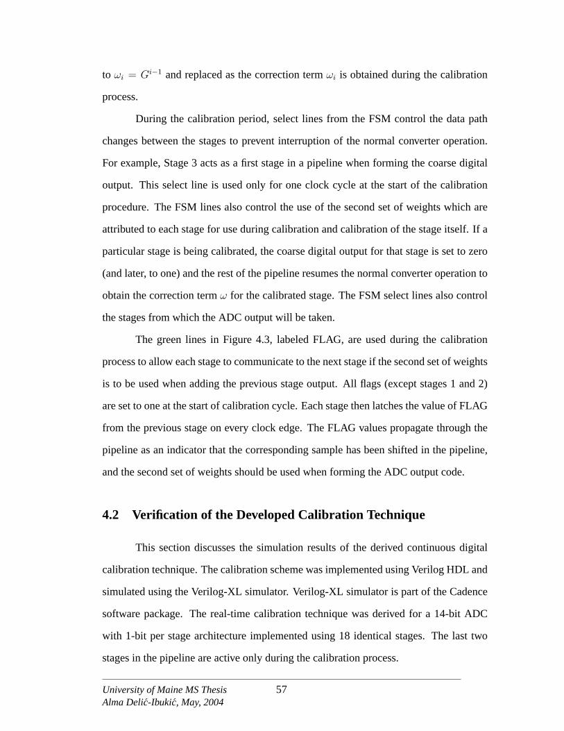
to ωi = Gi−1 and replaced as the correction termωi is obtained during the calibration
process.
During the calibration period, select lines from the FSM control the data path
changes between the stages to prevent interruption of the normal converter operation.
For example, Stage 3 acts as a first stage in a pipeline when forming the coarse digital
output. This select line is used only for one clock cycle at the start of the calibration
procedure. The FSM lines also control the use of the second set of weights which are
attributed to each stage for use during calibration and calibration of the stage itself. If a
particular stage is being calibrated, the coarse digital output for that stage is set to zero
(and later, to one) and the rest of the pipeline resumes the normal converter operation to
obtain the correction termω for the calibrated stage. The FSM select lines also control
the stages from which the ADC output will be taken.
The green lines in Figure4.3, labeled FLAG, are used during the calibration
process to allow each stage to communicate to the next stage if the second set of weights
is to be used when adding the previous stage output. All flags (except stages 1 and 2)
are set to one at the start of calibration cycle. Each stage then latches the value of FLAG
from the previous stage on every clock edge. The FLAG values propagate through the
pipeline as an indicator that the corresponding sample has been shifted in the pipeline,
and the second set of weights should be used when forming the ADC output code.
4.2 Verification of the Developed Calibration Technique
This section discusses the simulation results of the derived continuous digital
calibration technique. The calibration scheme was implemented using Verilog HDL and
simulated using the Verilog-XL simulator. Verilog-XL simulator is part of the Cadence
software package. The real-time calibration technique was derived for a 14-bit ADC
with 1-bit per stage architecture implemented using 18 identical stages. The last two
stages in the pipeline are active only during the calibration process.
University of Maine MS ThesisAlma Delic-Ibukic, May, 2004
57

++
G1
+G
0
� �� �� �� �� �� �
� �� �� � � �
DIG
ITA
L O
UT
PUT
OF T
HE
CO
NV
ER
TE
R
determined by the
finate state machine.
−
++
+
finite state machine
q1q2
GN
−2
G N
−1
+
GN
−1
q3
++
GN
−3
G
/G
q
N−
55
N−
3
5
q
G G02
qN+
1N
qN+
2
TW
O E
XT
RA
STA
GE
S USE
D D
UR
ING
CA
LIB
RA
TIO
N PR
OC
ESS
q
/
G G6
N−
4
N−
6
6
G
/G
q
N−
5
7N
−7
7
OB
TA
ININ
G C
OR
RE
CT
ION
TE
RM
S FO
R T
HE
STA
GE
S BE
ING
CA
LIB
RA
TE
D.
Stored digital value when
sub−D
AC
input is set to 0.
Sub−D
AC
input is set to 1.
for a stage
FLA
GFL
AG
FLA
G
FLA
G
FLA
GFL
AG
//
controlled by the
q
/
G G4
N−
2
N−
4
4
FLA
G1
2ω
ω3
/ω
ω
ωω
ω
FLA
GFL
AG
=0
Corrected w
eight
Figure
4.3:M
odifiederror
correctionlogic
fora
real-time
digitalcalibrationschem
eim
plementation.
Exam
pleof
N-stage
converter
with
1-bitperstage
architecture.
University of Maine MS ThesisAlma Delic-Ibukic, May, 2004
58

The design of the FSM was verified by comparing the Verilog simulation results
to the MATLAB simulation results discussed in Section3.4. The MATLAB simulation
was based on the foreground digital calibration technique. For both calibrations, the
digital calibration algorithm was the same and therefore, the final results should be
similar.
To verify that the derived real-time calibration technique works, it was necessary
to model a pipeline stage in Verilog HDL and also to control gain, threshold and sub-
DAC reference voltages of the stages being calibrated. To imitate the accurate behavior
of the pipeline ADC, fully digital odd and even stages were created using Verilog HDL.
Gain, threshold and sub-DAC reference voltages were made as controllable variables at
the input of each simulated pipeline stage. In order to compare MATLAB simulations
with Verilog HDL simulations, all ADC input signals, together with the gain, threshold,
and sub-DAC reference voltages were imported into the Verilog “test fixture”. Verilog
HDL is used to design digital logic, and as such accepts digital input signals only.
The decimal floating point values from MATLAB were converted to double precision
hexadecimal values and used as Verilog inputs.
The “test fixture” also contained two non-overlapping clock signals, the ‘reset’
and start of ‘calibration’ signals. The clock signals were distributed throughout the
pipeline accordingly. All the odd stages were active onφ1 and all the even stages were
active onφ2. The ‘reset’ signal was activated on the power up of the converter and it
was designated to write the required two sets of weights per stage. After initializing
each stage with the appropriate weights, the normal operation of the pipeline converter
can start and the ‘calibration’ signal can be activated at any instant.
The real-time calibration hardware model was tested using the test conditions
described in Section3.4. Here a sampling frequency of 51.2 MHz was used. The
sinusoidal test signal was set to 150 KHz with the amplitude at -1 dBFS. Errors, tabulated
University of Maine MS ThesisAlma Delic-Ibukic, May, 2004
59

in Table3.1, were introduced at different stages of the converter and 1024 samples were
used. Verilog-XL simulation results were collected and evaluated in MATLAB.
Figures4.4and4.5show the residual error characteristics for a simulated 14-bit
ADC calibrated in a real-time and calibrated using the foreground calibration technique
(on a converter power up). Errors for the various graphs were introduced at different
pipeline stages.
Figure4.4(a)shows the two calibration techniques implemented on a converter
with errors in the first stage only. Before activating the calibration signal, first stage
error contributions on the ADC final resolution can be seen. The ADC behaves as a
10-bit converter before calibration and as 12.5 bit converter after calibration. Once the
calibration signal is activated, 154 samples are needed for completion of the calibration
process. In Figure4.4(a), a consistent error increase in every 11th sample can be
observed. From the first calibration instant, every 11th sample corresponds to a start
of calibration. The 11th sample is the new input sample that will be routed as an input
to Stage 3 and therefore, skipping the error characteristics of Stage 1. This sample is the
only one to pass through the ideal converter (all 16 stages are ideal).
The goal of the digital calibration is to measure the converter errors, take these
as ‘nominal’ values of the converter and adjust the ADC output characteristics to match
these new nominal values. When compared to the ideal converter, the two output
characteristics will deviate from each other depending on the stage errors and redefined
‘nominal’ converter values. When implementing the derived continuous digital calibration,
if there is an error in a first stage only, there will be one sample that will propagate
through the converter with the ideal stages. In Figure4.4(a), a sample that propagates
through the ideal pipeline stages can be noticed as well as the difference between the
ideal and calibrated converter output characteristics. Figures4.4(b), 4.5(a), 4.5(b)show
successful real-time calibration of the converter with errors in more than one stage.
University of Maine MS ThesisAlma Delic-Ibukic, May, 2004
60

0 200 400 600 800 1000 1200−10
−5
0
5
10
15
20
25
30
35
40
45
Number of samples
Res
idua
l Err
or (
LSB
)
SFDR = 86.2033 dBSNRD = 77.4207 bitsENOB = 12.5682 bits
+2 LSB
−2 LSB
calib
ratio
n st
arts
foreground calibration (MATLAB)real−time calibration (Verilog HDL)
(a) Residual error characteristics with error contributions from the first stage only.
0 200 400 600 800 1000 1200−35
−30
−25
−20
−15
−10
−5
0
5
Number of samples
Res
idua
l Err
or (
LSB
) SFDR = 85.7562 dBSNRD = 77.2832 bitsENOB = 12.5454 bits
+2 LSB
−2 LSB
calib
ratio
n st
arts
foreground calibration (MATLAB)real−time calibration (Verilog HDL)
(b) Residual error characteristics with error contributions from the first two stages.
Figure 4.4: Residual error characteristics for a MATLAB simulated ADC with appliedforeground calibration (blue) and real-time calibration implemented in Verilog HDL(red).
University of Maine MS ThesisAlma Delic-Ibukic, May, 2004
61

0 200 400 600 800 1000 1200
−50
−40
−30
−20
−10
0
Number of samples
Res
idua
l Err
or (
LSB
)
SFDR = 85.0029 dBSNRD = 77.2251 bitsENOB = 12.5357 bits
+2 LSB
−2 LSB
calib
ratio
n st
arts
foreground calibration (MATLAB)real−time calibration (Verilog HDL)
(a) Residual error characteristics with error contributions from the first three stages.
0 200 400 600 800 1000 1200−10
−5
0
5
10
15
20
25
Number of samples
Res
idua
l Err
or (
LSB
)
SFDR = 93.7561 dBSNRD = 78.9281 bitsENOB = 12.8186 bits
+2 LSB
−2 LSB
calib
ratio
n st
arts
foreground calibration (MATLAB)real−time calibration (Verilog HDL)
(b) Residual error characteristics with the error contributions from the first sevenstages.
Figure 4.5: Residual error characteristics for a MATLAB simulated ADC with appliedforeground calibration (blue) and real-time calibration implemented in Verilog HDL(red) cont..
University of Maine MS ThesisAlma Delic-Ibukic, May, 2004
62

To re-calibrate the converter, only the calibration start signal needs to be provided.
Figure4.6 shows re-calibration of a 14-bit ADC with errors in a first stage only. First,
the converter was calibrated and weights for the first seven stages were adjusted accord-
ingly to give a resolution of 12.6 effective bits. Re-calibration occurred after a first
calibration was complete. Because the converter was just calibrated, it is reasonable
to assume that re-calibration should not affect the converter’s performance. However,
during the re-calibration process, the converter’s performance does degrade. The set of
weights used to form the output of the converter does not change with (re)calibration.
These weights are not programmable and therefore, when re-calibrating some samples
will show worse performance than others. This performance degradation can be avoided
by making the set of weights used during calibration programmable. If this is done, the
worse case performance of the converter during the re-calibration process will match the
output performance of the last conducted calibration.
4.3 Complexity of the Real-Time Calibration Logic
The complexity of the digital logic required to implement the derived real-time
calibration technique was evaluated using BuildGates Extreme synthesizer. The “worse
case” number of required logic gates was approximated. Area required for the calibration
logic was estimated using information from the International Technology Roadmap for
Semiconductors (ITRS) [18, 19].
Verilog modules needed to implement the calibration technique were imported in
BuildGates Extreme and synthesized using a ‘generic build’ command. This produces
unoptimized digital logic necessary to implement the real-time calibration technique.
The number of required transistor gates was approximated from the synthesized worse
case model. Approximately 100,000 logic gates are needed to implement the derived
real-time calibration technique. Figure4.7shows the calibration logic area requirements
with respect to the projected minimum feature size over a period of nine years. Data
University of Maine MS ThesisAlma Delic-Ibukic, May, 2004
63
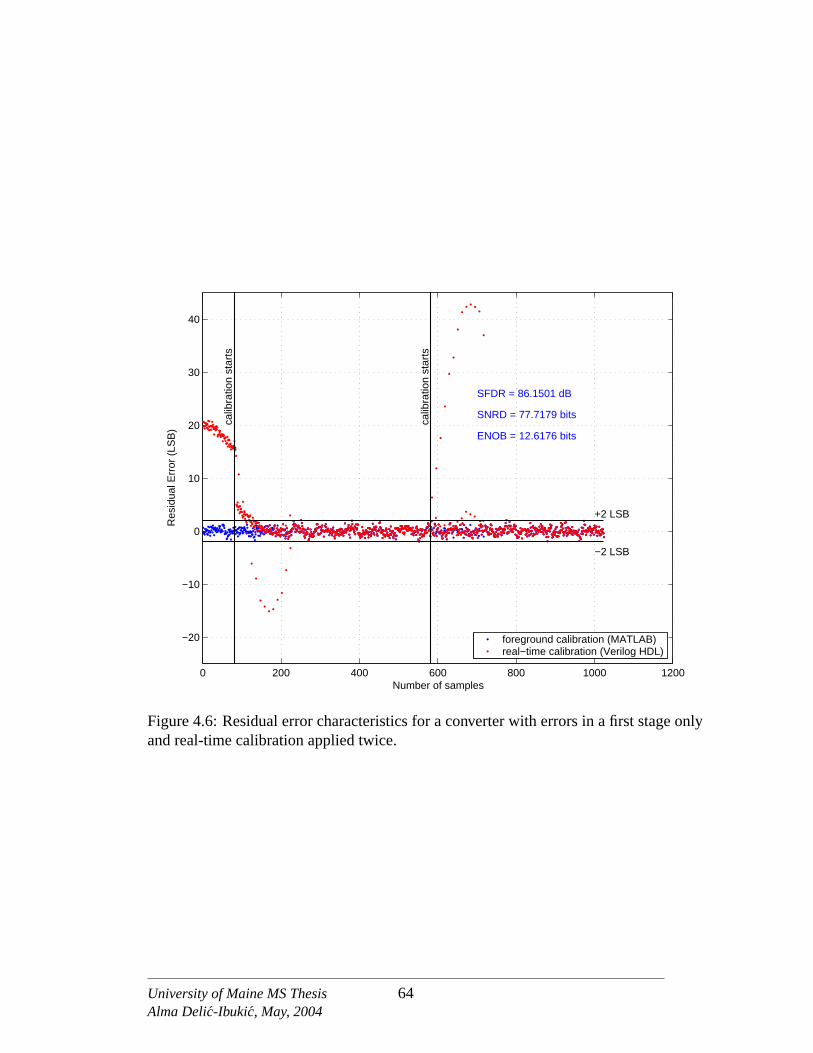
0 200 400 600 800 1000 1200
−20
−10
0
10
20
30
40
Number of samples
Res
idua
l Err
or (
LSB
)
SFDR = 86.1501 dB
SNRD = 77.7179 bits
ENOB = 12.6176 bits
+2 LSB
−2 LSB
calib
ratio
n st
arts
calib
ratio
n st
arts
foreground calibration (MATLAB)real−time calibration (Verilog HDL)
Figure 4.6: Residual error characteristics for a converter with errors in a first stage onlyand real-time calibration applied twice.
University of Maine MS ThesisAlma Delic-Ibukic, May, 2004
64
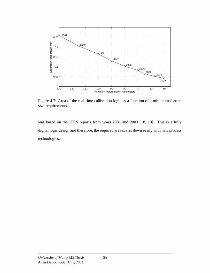
50607080901001101201300
0.05
0.1
0.15
0.2
0.252001
2002
2003
2004
2005
20062007
2008
2009
Cal
ibra
tion
logi
c ar
ea in
mm
2
Minimum feature size in nanometers
Figure 4.7: Area of the real-time calibration logic as a function of a minimum featuresize requirements.
was based on the ITRS reports from years 2001 and 2003 [18, 19]. This is a fully
digital logic design and therefore, the required area scales down easily with new process
technologies.
University of Maine MS ThesisAlma Delic-Ibukic, May, 2004
65
CHAPTER 5
Conclusion
Different calibration techniques targeted to pipeline ADCs have been proposed
in the literature and successfully implemented. Most of the reported calibration schemes
rely on the converter being off line while calibrated or are analog in nature. Analog
schemes are generally more difficult to scale to new process technologies due to the
increase in sub-threshold and gate leakage currents and reduced power supply voltage
[13]. This thesis expanded on a digital calibration algorithm developed by Karanicolas
et al. [4] and derived a novel continuous digital calibration scheme targeted for pipeline
ADCs. A hardware model of the continuous digital calibration logic was designed using
Verilog HDL and it was effective in showing the success of the continuous calibration
technique. The calibration technique derived in this thesis is completely digital and
transparent to the overall system. It is realized using two extra stages located at the end
of the pipeline. These stages are used only during the calibration process.
Dominant static error contributions for pipeline ADCs were defined and discussed.
These included comparator offset (sub-ADC error), charge injection (sub-DAC errors)
and capacitor mismatch gain errors. The digital calibration algorithm derived in [4]
was simulated in MATLAB and demonstrated using a 1-bit per stage pipeline archi-
tecture. The algorithm was successful in correcting for all of the above mentioned stage
nonlinearities. The algorithm was expanded to work in real-time without interrupting
the normal operation of the converter. Verilog HDL was used to model the real-time
digital calibration scheme and hardware simulation was performed using Verilog-XL.
The simulation results verified the success of the derived calibration scheme and
showed the dominance of converter errors introduced at the front end of the pipeline.
Also, the importance of the sub-ADC, sub-DAC and interstage gain errors was shown.
For the simulated ADC, the number of effective bits was improved by 3 bits and the
University of Maine MS ThesisAlma Delic-Ibukic, May, 2004
66

dynamic range of the converter was improved by 20 dB. A rough estimate of the complexity
of the calibration scheme was obtained using the BuildGates Extreme digital circuit
synthesizer. The required area to implement the necessary digital logic scales down
easily with the new process technologies, making it an attractive solution for calibration
of pipeline converters.
Additional research is required to demonstrate the calibration technique on a real
14-bit, 50 MHz pipeline ADC. This can be accomplished by designing a 14-bit ADC
with 1-bit per stage topology, gains less than two and having intermediate bits as the
outputs of the converter. Additional digital input lines for each calibrated stage must also
be provided in order to allow the calibration logic to specify the digital stage outputs, or
ground the stage inputs. These could provide inputs to an FPGA (Field Programmable
Gate Array) where the continuous digital calibration and error correction logic resides.
This way the power consumption of the digital calibration logic can be examined, and
the effectiveness of the derived calibration in hardware evaluated.
University of Maine MS ThesisAlma Delic-Ibukic, May, 2004
67

REFERENCES
[1] E. Brunner, “Ultrasound system considerations and their impacton front-end components,” tech. rep., Analog Devices, Inc., 2002.http://www.analog.com/library/analogDalogue/archives.
[2] E. G. Soenen and R. L. Geiger, “An architecture and an algorithm for fully digitalcorrection of monolithic pipelined ADC’s,”IEEE Transactions on Circuits andSystems-II, vol. 42, pp. 143–153, Mar. 1995.
[3] J. M. Ingino and B. A. Wooley, “A continuously calibrated 12-b, 10-MS/s, 3.3vA/D converter,”IEEE Journal of Solid-State Circuits, vol. 12, pp. 1920–1931, Dec.1998.
[4] A. N. Karanicolas, H.-S. Lee, and K. L. Bacrania, “A 15-b 1-Msample/s digitallyself-calibrated pipeline ADC,”IEEE Journal of Solid-State Circuits, vol. 28,pp. 1207–1215, Dec. 1993.
[5] S.-H. Lee and B.-S. Song, “Digital-domain calibration of multistep analog-to-digital converter,”IEEE Journal of Solid-State Circuits, vol. 27, pp. 1679–1688,Dec. 1992.
[6] H.-S. Lee, D. A. Hodges, and P. R. Gray, “A self-calibrated 15 bit CMOS A/Dconverter,”IEEE Journal of Solid-State Circuits, vol. 6, pp. 813–819, Dec. 1984.
[7] Y.-M. Lin, B. Kim, and P. R. Gray, “A 13-b 2.5-MHz self-calibrated pipelinedA/D converter in 3-micron CMOS,”IEEE Journal of Solid-State Circuits, vol. 26,pp. 628–636, Apr. 1991.
[8] J. Ming and S. H. Lewis, “An 8-bit 80-Msample/s pipelined analog-to-digitalconverter with background calibration,”IEEE Journal of Solid-State Circuits,vol. 36, pp. 1489–1497, Oct. 2001.
[9] H.-S. Lee, “A 12- 600 ks/s digitally self-calibrated pipelined algorithmic ADC,”IEEE Journal of Solid-State Circuits, vol. 29, pp. 509–515, Apr. 1994.
[10] I. E. Opris, L. D. Lewicki, and B. C. Wong, “A single-ended 12-bit 20 Msample/sself-calibrating pipeline A/D converter,”IEEE Journal of Solid-State Circuits,vol. 33, pp. 1898–1903, Dec. 1998.
[11] K. Sockalingam, “Error compensation in pipeline A/D converters,” Master’s thesis,University of Maine, Orono, 2002.
[12] T.-H. Shu, B.-S. Song, and K. Bacrania, “A 13-b 10-Msample/s ADC digitallycalibrated with oversampling delta-sigma converter,”IEEE Journal of Solid-StateCircuits, vol. 30, pp. 443–452, Apr. 1995.
[13] A. Abo, Design for Reliability of Low-voltage Switched-capacitor Circuits. PhDthesis, University of California, Berkeley, California, May 1999.
University of Maine MS ThesisAlma Delic-Ibukic, May, 2004
68

[14] “AMI Foundry Capabilities,” 2003. www.amis.com/foundy/cmos.html.
[15] B. J. Sheu and C. Hu, “Switch-induced error voltage on a switch capacitor,”IEEEJournal of Solid-State Circuits, vol. 19, pp. 519–525, Aug. 1984.
[16] G. Wegmann, E. A. Vittoz, and F. Rahali, “Charge injection in analog MOSswitches,” IEEE Journal of Solid-State Circuits, vol. 22, pp. 1091–1097, Dec.1987.
[17] W. B. Wilson, H. Z. Massoud, E. J. Swanson, R. T. George, and R. B. Fair,“Measurement and modeling of charge feedthrough in n-channel MOS analogswitches,” IEEE Journal of Solid-State Circuits, vol. 20, pp. 1206–1213, Dec.1985.
[18] “International Technology Roadmap for Semiconductors 2001 Edition,” 2001.http://public.itrs.net.
[19] “International Technology Roadmap for Semiconductors 2003 Edition,” 2003.http://public.itrs.net.
[20] U.-K. Moon and B.-S. Song, “Background digital calibration techniques forpipelined ADC’s,”IEEE Transactions on Circuits and Systems-II, vol. 44, pp. 102–109, Feb. 1997.
[21] X. Wang, P. Hurst, and S. Lewis, “A 12-bit 20 MS/s pipelined ADC with nesteddigital background calibration,” inProceedings of IEEE Custom IC Conf., (SanJose), pp. 409–412, Sept. 2003.
[22] D. J. Smith,HDL Chip Design. Madison, AL: Doone Publications, 1996.
University of Maine MS ThesisAlma Delic-Ibukic, May, 2004
69

BIOGRAPHY OF THE AUTHOR
Alma Delic-Ibukic was born in Bihac, Bosnia-Herzegovina on October 20th,
1978. She received her high school education from Mount Desert Island High School
in Bar Harbor, Maine graduating in 1997. She entered the University of Maine in 1997
and obtained her Bachelor of Science degree in Electrical Engineering in 2002. During
her undergraduate education, she completed a semester long Co-op assignment at Texas
Instruments Inc. (Dallas, TX) where she worked on test and characterization of high-
speed ADCs.
In September 2002, she was enrolled for graduate study in Electrical Engineering
at the University of Maine and served as a Research Assistant in the Communications
and Signal Processing Laboratory. Her current research interests include communica-
tions, signal processing and mixed-signal CMOS design, such as high-speed ADCs.
She is a member of IEEE, Tau Beta Pi and Eta Kappa Nu. Alma is a candidate
for the Master of Science degree in Electrical Engineering from The University of Maine
in May, 2004.
University of Maine MS ThesisAlma Delic-Ibukic, May, 2004
70