computer simulation of electromigration in
TRANSCRIPT

Computer Simulation of
ElectroMigration in Microelectronics
Interconnect
by Xiaoxin Zhu Centre of Numerical Modelling and Process Analysis, School of Computing and Mathematical Sciences,The University of Greenwich, London, U.K. A thesis submitted in partial fulfillment of the requirements of the University of Greenwich for the Degree of Doctor of Philosophy July 2014

DECLARATION I certify that this work has not been accepted in substance for any degree, and is not concurrently being submitted for any degree other than that of Doctor of Philosophy being studied at the University of Greenwich. I also declare that this work is the result of my own investigations except where otherwise identified by references and that I have not plagiarised the work of others. …………………………………………………………………. Xiaoxin Zhu (PhD student) …………………………………………………………………. Hua Lu (Supervisor) …………………………………………………………………. Christopher Bailey (Supervisor)

i
Abstract
Electromigration (EM) is a phenomenon that occurs in metal conductor carrying high density
electric current. EM causes voids and hillocks that may lead to open or short circuits in
electronic devices. Avoiding these failures therefore is a major challenge in semiconductor
device and packaging design and manufacturing, and it will become an even greater
challenge for the semiconductor assembly and packaging industry as electronics components
and interconnects get smaller and smaller. According to the assembly and packaging section
of the International Technology Roadmap for Semiconductor (ITRS) developed in 2007 and
2009 [1] [2], EM was a near term threat for the interconnecting part of semiconductor,
devices and packaging methods such as flip chip, and Ball Grid Array (BGA).
In the industry, EM-aware designs are mainly based on design rules that are derived from
empirical laws which do not help understand complicated EM processes and therefore can’t
be used to carry out accurate predictions for EM failures of sophisticated components in
varied environmental conditions. In this work, novel numerical modelling methods of EM in
micro-electronics devices have been developed and the methods have been used to analyse
EM process in a lead free solder thin film, and to optimize the design of electronic
components in order to reduce the risk of EM relative failure.
EM is an atomic diffusion process that is driven by a high density electric current, but it is
strongly affected by temperature and its gradient as well as stress distribution. In order to
model EM accurately, the interacting electrical, thermal, and mechanical phenomena must all
be solved simultaneously. In this work, a novel multi-physics modelling method has been
proposed and developed to include all of the above mentioned physical phenomena using
unstructured Finite Volume (FV) and Finite Element (FE) techniques. The methods have
been implemented on the multi-physics software package PHYSICA. Comparing with
existing methods, this fully coupled solution method is a significant improvement that will
facilitate further development of electronics design and optimization tool as well as new
research work that helps understand EM phenomenon. The developed models can be used to

ii
simulate the whole process of EM, predict voids initiation lifetime of electronics products or
test specimens.
In today’s electronics manufacturing, lead-free solder alloys are used as interconnect. As in
copper or aluminium interconnect EM has become a threat to device reliability as current
density increase in solder joints with diminishing sizes. In this work, computer simulation
methods have been used to analyse the experimentally observed EM process in a thin film
solder. The experiment was designed in such a way that effects of temperature and stress
gradients can be avoided. The advantage of this experimental method is that the electric
current effect is isolated which makes analysis and model validation easier. In this work, the
predicted voids locations are consistent with experimental results.
In this work, numerical examples are given to illustrate how interconnect designs can be
made more EM failure resistant. The ultimate aim of the research is to understand EM and to
develop techniques that predict EM accurately so that EM-aware designs can be made easier.

iii
ACKNOWLEDGEMENTS
Firstly, I would like to express my gratitude to my supervisors Dr. Hua Lu and Professor
Christopher Bailey for their kind advice, encouragement and guidance throughout my PhD
studies.
I would like to acknowledge Professor Samjid H. Mannan and Dr. Hiren Kotadia from King’s
College, London, Professor Y.C. Chan and Ms Sha Xu from the City University of Hong
Kong for their advice and help in experiments. I would also like to acknowledge Dr. Georgi
Djambazov for helping me understand the structure of PHYSICA.
I would like to thank my parents for their understanding and complete support and also my
friends for their entertaining distractions and polite interest.
Finally, I would like to acknowledge the University of Greenwich without its financial
support I could not have carried out my research.

iv
Table of Contents Declaration Abstract .................................................................................................................................................................... i Acknowledgements ......................................................................................................................................... iii List of Figures .................................................................................................................................................... vii List of Tables ..................................................................................................................................................... xiii List of Publication ........................................................................................................................................... xiv Chapter 1 INTRODUCTION ............................................................................................................................ 1
1.1 Electromigration and Microelectronics Reliability ........................................................................ 1
1.2 Electronic Packaging and Its Trend ............................................................................................... 3
1.3 Aims and Objectives of This Research .......................................................................................... 9
1.4 Challenges and Methodologies ..................................................................................................... 9
1.5 Contribution of This Study .......................................................................................................... 10
1.6 The Structure of The Thesis ........................................................................................................ 11 Chapter 2 A REVIEW ON ELECTROMIGRATION PHENOMENON AND RESEARCH METHODOLOGY ............................................................................................................................................... 13
2.1 Overview of The Chapter ............................................................................................................ 13
2.1.1 The EM Phenomenon........................................................................................................... 13
2.1.2 The Thermomigration Phenomenon ................................................................................... 14
2.1.3 The Stressmigration Phenomenon ...................................................................................... 15
2.1.4 EM and Conductor Materials ............................................................................................... 15
2.1.5 The Effects of Interfacial Chemical Reactions ...................................................................... 16
2.1.6 AC or DC? ............................................................................................................................. 16
2.2 EM Modelling Approaches .......................................................................................................... 21
2.2.1 Empirical Approaches of EM Analysis .................................................................................. 21
2.2.2 Numerical Approaches of EM Analysis ................................................................................ 24
2.2.2.1 EM and Mechanical Stress Effect ...................................................................................... 25

v
2.2.2.2 EM and Thermal Effect...................................................................................................... 27
2.2.2.3 Generation /Annihilation Term ......................................................................................... 28
2.2.2.4 Void Nucleation ................................................................................................................ 29
2.2.2.5 Damage Mechanics/Measurement .................................................................................. 31
2.2.2.6 Molecular Dynamics Model .............................................................................................. 33
2.2.3 EM Modelling Methodologies .............................................................................................. 35
2.2.3.1 Atoms/Vacancies Condensation at Boundary .................................................................. 36
2.2.3.2 Atomic/Vacancy Flux Divergence Based Analysis ............................................................. 41
2.2.3.2 Voids Formation and Evolution Simulation ...................................................................... 44
2.2.3.3 Other Void Simulation Methods ....................................................................................... 45
2.3 Conclusion ................................................................................................................................... 45 CHAPTER 3: EM IN THIN SOLDER FILM ............................................................................................... 47
3.1 Introduction ................................................................................................................................ 47
3.2 Experimental Details ................................................................................................................... 48
3.3 Experimental Results................................................................................................................... 49
3.4 Coupled Electrical and Thermal Analysis .................................................................................... 53
3.5 Evolution of Voids ...................................................................................................................... 57
3.6 Divergence of Atomic Flux ......................................................................................................... 59
3.7 EM and Current Density Gradient ............................................................................................... 62
3.8 Conclusion ................................................................................................................................... 63 Chapter 4: MULTI-PHYSICS MODEL DEVELOPMENT AND IMPLEMENTATION ................. 64
4.1 Introduction ................................................................................................................................ 64
4.2 Modelling Methodology ............................................................................................................. 64
4.2.1 General Scalar Transport Equations .................................................................................... 65
4.2.2 Electric current and joule heating ........................................................................................ 66
4.2.3 Heat transfer ........................................................................................................................ 66
4.2.4 Structural Mechanics Module .............................................................................................. 67
4.3 Implementation .......................................................................................................................... 69
4.3.1 One Dimensional Model with Pure Electrical Effect ............................................................ 70
4.3.2 Back Stress Effect ................................................................................................................. 71
4.3.3 Thermal Effect and Thermally Induced Stress Effect. .......................................................... 77
4.3.4 Void Evolution ...................................................................................................................... 81
4.3.5 Convection-diffusion Boundary Conditions ......................................................................... 88
4.3.6 Atomic/Vacancy Flux Divergence ......................................................................................... 91

vi
4.4 Case Study ................................................................................................................................... 94
4.4.1 Model setup ............................................................................................................................. 94
4.4.2 EM Analysis and Void Evolution ............................................................................................... 97
4.4.3 Analysis of Thermal Effects .................................................................................................... 101
4.4.4 Analysis of Stress Effects ....................................................................................................... 103
4.5 Conclusion ................................................................................................................................. 106 CHAPTER 5: EM AWARE DESIGN ........................................................................................................... 108
5.1 Introduction .............................................................................................................................. 108
5.2 Design Factors ........................................................................................................................... 108
5.2.1 Material Selection .............................................................................................................. 108
5.2.2 Back Stress and Critical Length .......................................................................................... 109
5.2.3 Bamboo Structure and Slotted Wires ................................................................................ 111
5.2.4 Reservoir Effect .................................................................................................................. 112
5.3 Conductor Design and Optimization ......................................................................................... 113
5.3.1 Interconnects Design and Optimization ............................................................................ 113
5.3.2 Corner Angle and Via Arrangement ................................................................................... 115
5.3.3 Mitigate Current Crowding in Solder Joint ........................................................................ 117
5.4 EM-Aware Design Rule and Standard Processing ..................................................................... 121
5.4.1 Current-Driven Routing Module ........................................................................................ 123
5.4.2 EM-robust Verification Module ......................................................................................... 125
5.4.3 EM-robust Optimization Module ....................................................................................... 127
5.5 Conclusion ................................................................................................................................. 128 CHAPTER 6: CONCLUSION AND FUTURE WORK ........................................................................... 129
6.1 Conclusion ................................................................................................................................. 129
6.2 Future Work .............................................................................................................................. 130 REFERENCES .................................................................................................................................................. 132

vii
List of Figures Figure 1.1: The polycrystalline structure of metal. .. .................................................................. 2
Figure 1.2: The driving force of EM is mainly the momentum transfer from conducting
electrons to diffusing ions. .. ....................................................................................................... 2
Figure 1.3: Hillocks may appear at the anode and voids may appear at the cathode.. ............... 3
Figure 1.4: Components for standard PTH electronics packages (60’s - 70’s). ......................... 4
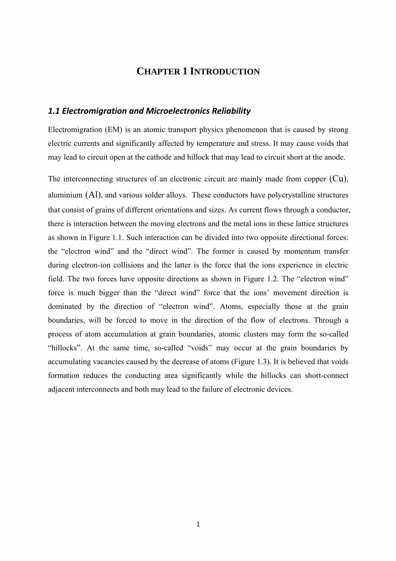
Figure 1.5: Components for standard SMP electronics packages (70’s - 80’s).. ........................ 4
Figure 1.6: Left: the structure schematic of a SMP component. Right: the structure schematic
of an area array packaging component.. ..................................................................................... 5
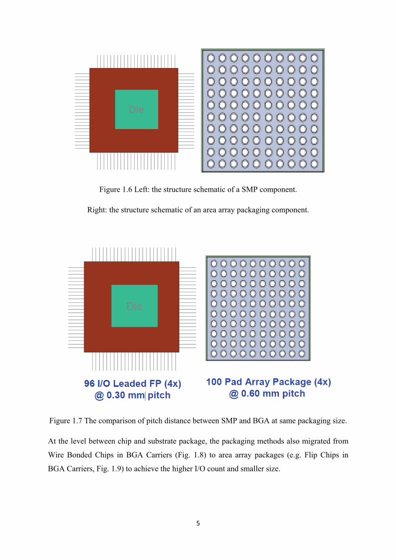
Figure 1.7: the comparison of pitch distance between SMP and BGA at same packaging size. 5
Figure 1.8: Left: the schematic of wire bond structure.Right: IBM’s organic BGA carrier built
by endicott interconnect, chips are attached by fine gold wire bonds. ....................................... 6
Figure 1.9: Left: the schematic of flip chip structure. Right: Intel 90nm Pentium 4
microprocessor in an organic flip chip ball grid array carrier.. .................................................. 6
Figure 1.10: IBM’s (EI’s) High Performance Chip Carrier (HPCC). ......................................... 7
Figure 1.11: The trend in flip chip package according to ITRS 2003. .. .................................... 8
Figure 2.1: SEM images of morphological on a eutectic SnPb solder bar due to EM after
applying 2.8 x 10⁴ A/cm2 at 150 ºC for 8 days: (a) The hillock at the anode (b) voids at the
cathode due to EM.. .................................................................................................................. 13
Figure 2.2: Photograph of failure site in 800- µm -long, 1.2- µm-wide, and 0.08-µm-thick
stripe under pure AC stressing and a SEM of the failure site. AC: J=1.0x10⁷ A/cm2, 25MHz,
T=250 ºC. .................................................................................................................................. 18
Figure 2.3: In pure AC condition, the void grows during the first half cycle in (a) and
decreases during the opposite current period in (b). As a result, the triple point becomes an
atomic flux blocker for particular direction .............................................................................. 18
Figure 2.4: Current density waveforms at different duty cycles (r) and peak current densities
(Jpeak);.. .................................................................................................................................... 20
Figure 2.5: Schematic diagram of current flow in the Blech structure. .................................... 22

viii
Figure 2.6: Schematic diagram of void nucleation at an interface site of weak adhesion. ....... 30
Figure 2.7: Grain boundary structure, 264 fixed atoms, 510 free and 9 layers stacked in z-
direction.. .................................................................................................................................. 34
Figure 2.8: Trace of atomic trajectory where any atoms that move beyond inter atomic
distance between nearest neighbors.. ........................................................................................ 35
Figure 2.9: The semi-infinite grain boundary proposed by Shatzkes and Llyod. ..................... 37
Figure 2.10: Vacancy concentration at the blocking boundary at x=0 for the semi-infinite line,
and the finite-line.. .................................................................................................................... 38
Figure 2.11: Vacancy concentration along the line at different time according to De Groot
SR’s analytic solution. .............................................................................................................. 39
Figure 2.12: Model of two grain boundaries intersecting at x=0 .............................................. 40
Figure 3.1: (a) Plan view of specimen geometry and (b) electrical setup. ................................ 49
Figure 3.2: (a) AFM image of sample topography and (b) SEM image of solder thin film
cross section. ............................................................................................................................. 50
Figure 3.3: Void distribution of sample 1 observed optically in transmission where the sample
is represented by the dark area and voids by the bright spots. .................................................. 51
Figure 3.4: SEM images of sample 1 at increasingly higher magnification scale (top to
bottom). The small red circle in the top left image is shown magnified in the bottom left
image. The scale bars in the micrographs from top down are 200, 20 and 10 microns
respectively. .............................................................................................................................. 52
Figure 3.5: Void and hillock distribution of sample 2 that are observed a) optically and b) by
SEM. ......................................................................................................................................... 53
Figure 3.6: The geometry of FEA model and the boundary conditions. .................................. 54
Figure 3.7: Mesh condition of simulation. ................................................................................ 55
Figure 3.8: Temperature distribution (°C) from a 3D model, which included solder, copper
substrate and glass slide for sample 1; the light blue line located in the centre of model is the
edge of glass slide.. ................................................................................................................... 56
Figure 3.9: Temperature (Unit: °C) distribution for solder film only for sample 1.. ................ 56
Figure 3.10: (a) Initial current density distribution (Unit: MA/m2). (b) Current density
distributions. The void has a size of two elements. (c) Current density distributions. The void

ix
has a size of eight elements. (d) Current density distributions. The void has a size of eighteen
elements.. .................................................................................................................................. 58
Figure 3.11: Highest current density as number of removed/dead elements increased.. .......... 59
Figure 3.12: Resistance changes as void grows in size. ........................................................... 59
Figure 3.13: Atomic flux distributions around the void. .. ....................................................... 61
Figure 3.14: The divergence of atomic flux at time 556 hours. ................................................ 61
Figure 3.15: Current density gradient distributions. ................................................................. 62
Figure 4.1: Flow Chart of the EM model. ................................................................................. 65
Figure 4.2: Components of stress.............................................................................................. 67
Figure 4.3: The schematic diagram of boundary conditions..................................................... 70
Figure 4.4: The normalized vacancy concentration distribution in (a) graph and (b) contour at
time: 10s, 100s, and 800s. .. ...................................................................................................... 71
Figure 4.5: The normalized vacancy concentration distribution coupled stress effect in (a)
graph and (b) contour at time: 10s, 100s, and 800s. ............................................................... 74
Figure 4.6: The Von Mises Stress distribution (Unit: Pa) at time: (a) 10s, (b) 100s, and (c)
800s. .......................................................................................................................................... 75
Figure 4.7: The hydrostatic stress distribution along with the Al strip at time 10s 100s and
800s.. ......................................................................................................................................... 75
Figure 4.8: Time to reach certain Von Mises Stress (a) 100 MPa and (b) 200 MPa at the
cathode shows the trend that it strongly depends on the inverse of the square of current
density. . ................................................................................................................................... 76
Figure 4.9: The normalized vacancy concentration distribution coupled thermal effect in (a)
graph and (b) contour at time: 10s, 100s, and 800s.. ................................................................ 78
Figure 4.10: The normalized vacancy concentration distribution coupled thermal effect
(reverse temperature loading) in (a) graph and (b) contour at time: 10s, 100s, and 800s.. ...... 78
Figure 4.11: Temperature distribution and deformation due to thermal expansion (Unit: °C,
deformation scaling factor: 100).. ............................................................................................. 79
Figure 4.12: Hydrostatic stress distribution (Unit: Pa).. ........................................................... 80
Figure 4.13: Hydrostatic stress gradient distribution (Unit: Pa/µm).. ...................................... 80
Figure 4.14: The normalized vacancy concentration distribution coupled thermal stress effect
in (a) graph and (b) contour at time: 10s, 100s, and 800s. ........................................................ 81

x
Figure 4.15: The normalized vacancy concentration distribution coupled thermal stress effect
(reverse temperature loading) in (a) graph and (b) contour at time: 10s, 100s, and 800s.. ...... 81
Figure 4.16: The relationship between voids growth and EM driving forces. ......................... 82
Figure 4.17: Procedure of void evolution judgement. .. ........................................................... 83
Figure 4.18: A 2-D testing structure and current density distribution (Unit: A/µm2). ............. 84
Figure 4.19: Voids evolution, red element indicates “dead element” (a) to (j) are time step 2
to time step 11.. .. ...................................................................................................................... 84
Figure 4.20: Current density distribution change due to voids evolution, (a) to (j) are time
step 2 to time step 11.. .............................................................................................................. 85
Figure 4.21: Structure, boundary condtion and mesh condtion and normalized vacancy
concentration distritbution at time 10s. ..................................................................................... 86
Figure 4.22: Voids growth at time (a) 17s (b) 33s (c) 42s (d) 48s (e) 51s (Red elements
represent the “dead elements”). ................................................................................................ 87
Figure 4.23: The recorded maximum vacancy concentration evolution at time (a) 17s (b) 33s
(c) 42s (d) 48s (e) 51s. .............................................................................................................. 87
Figure 4.24: The atomic flux at the material boundary. ........................................................... 88
Figure 4.25: Material boundary treatment method. .................................................................. 89
Figure 4.26: The schematic diagram of model, two tungsten lines are set to form a material
interface which should stops the atomic/vacancy flux due to low diffusivity of tungsten. .. ... 89
Figure 4.27: Shows the effect of blocking the convective flux at the material boundary on the
vacancy concentration. .............................................................................................................. 90
Figure 4.28: The schematic diagram of a via interconnecting structure and boundary
conditions in the numerical simulation. .................................................................................... 92
Figure 4.29: (a) Current density distribution of Blech model. (b) Temperature distribution of
Blech model. (c) Hydro-static stress distribution of Blech model. .. ........................................ 92
Figure 4.30: (a) Vacancy flux divergence distribution due to EM at time = 2000s. (b)
Vacancy flux divergence distribution due to TM at time = 2000s. (c) Vacancy flux
divergence distribution due to SM at time = 2000s. ................................................................. 93
Figure 4.31: The temperature gradient distribution (Unit: K). ................................................. 94
Figure 4.32: The structure, boundary condition and mesh condition. ...................................... 95
Figure 4.33: The current density distribution (Unit: A/µm2). .. ............................................... 95
xi
Figure 4.34: The temperature distribution (Unit: °C). .............................................................. 95
Figure 4.35: The displacement distribution (Unit: µm) and deformation (Deformation scaling
factor: 75) .. ............................................................................................................................... 96
Figure 4.36: The effective stress distribution (Unit: Pa) and deformation (Deformation scaling
factor: 75). ................................................................................................................................. 96
Figure 4.37: The temperature gradient distribution (Unit: °C/µm) ......................................... 97
Figure 4.38: The hydrostatic stress gradient distribution (Unit: Pa/µm) .. ............................... 98
Figure 4.39: The normalized vacancy distribution at time 10s.. ............................................... 98
Figure 4.40: The normalized vacancy distribution of bottom Al strip at time (a) 10s (b) 100s
and (c) 800s. .. ........................................................................................................................... 99
Figure 4.41: Voids growth at time (a) 17s (b) 33s (c) 42s (d) 48s (e) 51s (Red elements
represent the “dead elements”). .. ........................................................................................... 100
Figure 4.42: The recorded maximum vacancy concentration evolution at time (a) 17s (b) 33s
(c) 42s (d) 48s (e) 51s . .. ........................................................................................................ 100
Figure 4.43: The drift velocity distribution in value and in vector of thermal effect only (the
length of vector represents intensity of drift velocity). (a) drift velocity distribution (Unit:
µm/s), (b) vacancy flux vector and (c) atomic flux vector.. .. ................................................ 102
Figure 4.44: The normalized vacancy concentration distribution driven by (a) coupled self-
diffusion and electrical effects and (b) coupled self-diffusion, electrical effect and thermal
effects at time 10s. . .. ............................................................................................................. 103
Figure 4.45: The drift velocity distribution in value and in vector of thermal stress effect only
(the length of vector represents intensity of drift velocity). (a) drift velocity distribution (Unit:
µm/s), (b) vacancy flux vector and (c) atomic flux vector.. .. ................................................ 104
Figure 4.46: The normalized vacancy concentration distribution driven by (a) coupled self-
diffusion and electrical effects and (b) coupled self-diffusion, electrical effect and thermal
stress effects at time 10s.. .. .................................................................................................... 104
Figure 4.47: The normalized vacancy concentration distribution driven by (a) coupled self-
diffusion and electrical effects and (b) coupled self-diffusion, electrical effect, thermal effect,
thermal stress effects and back stress effect at time 10s.. .. .................................................... 106
Figure 5.1: SEM image of two-level Al (Cu) interconnect lines with W-plug vias on a Si
surface. The width of the line and the spacing between them is 0.5 µm.. .. ........................... 110

xii
Figure 5.2: Reduced wire width – less than the average grain size – improves wire reliability
with regard to EM. .. ............................................................................................................... 111
Figure 5.3: Reservoir effect: (a) a regular via structure without overhang (b) a via structure
with overhang. ........................................................................................................................ 113
Figure 5.4: Schematic cross section area of conductor. .. ....................................................... 114
Figure 5.5: Current density distributions of corners with different angles. (Units: A/m2). .. 116
Figure 5.6: Current crowding can be reduced by rearranging tungsten via array. .. ............... 116
Figure 5.7: The structure of a typical solder joint. .................................................................. 117
Figure 5.8: The cross section view of the current distribution of a typical solder joint. The
cycled area is the current crowding site. ................................................................................. 118
Figure 5.9: (a) Basic structure without current division, (b) 1/2 shunt structure, (c) 1/4 shunt
structure and (d) 1/8 shunt structure. ...................................................................................... 119
Figure 5.10: Top view of the current density distribution in solder joints (Unit: A/m2).. ..... 119
Figure 5.11: The top view of the current density (A/m2) distributions in solder bump ......... 120
Figure 5.12: The flow chart of modern IC design. ................................................................. 121
Figure 5.13: The flow chart of proposed EM-aware design process. ..................................... 122
Figure 5.14: The schematic diagram of the suggested current-driven routing stage.. ............ 123
Figure 5.15: The different current flow patterns within different net topologies. .................. 124
Figure 5.16: The schematic diagram of the suggested EM-Robust verification module. ....... 125
Figure 5.17: The schematic diagram of the suggested EM-Robust optimization module. ..... 126
Figure 5.18: (a) Net with “violating” area (pink area representing “violating” area is with
high current density) compare to (b) Optimization net (green areas are optimized by wire &
via-array sizing part, red areas are optimized by the addition of a support structure part).. ..127

xiii
List of Tables
Table 2.1: Parameters used in the calculations. ........................................................................ 38
Table 2.2: The contribution of the three terms in energy balance equation (Assuming the
substrate thickness is 300 µm and current density is 1MA/cm2). ............................................. 43
Table 3.1: Parameters for thermal analysis. .............................................................................. 55
Table 3.2: Parameters for diffusion-convection model. ............................................................ 60
Table 4.1: Parameters used in the calculations. .. ..................................................................... 71
Table 4.2: Time to reach certain Von Mises stress at the cathode with different current
densities..................................................................................................................................... 76
Table 4.3: Parameters used in modelling. ................................................................................. 86
Table 4.4: Maximum atomic flux divergences due to EM, TM and SM with initial atomic
concentration Cv0=1. ................................................................................................................. 93
Table 5.1: EM resistance comparison between pure Al and Al/Cu. The higher Blech product
value of Al/Cu alloy means it has higher EM resistance than pure Al.. ................................. 109
Table 5.2: Parameters. ............................................................................................................. 109
Table 5.3: The drift velocity comparison for different activation energy Ea.. ........................ 109

xiv
List of Publication
• X. Zhu, H. Kotadia, S. Xu, H. Lu, S. H. Mannan, C. Bailey, Y.C. Chan, Multi-Physics
Computer Simulation of the Electro-migration , proceedings of the International
Conference on Electronic Packaging Technology & High Density Packaging (ICEPT-
HDP 2011) in Shanghai, China 2011
• X. Zhu, H. Kotadia, S. Xu, H. Lu, S. H. Mannan, C. Bailey, Y.C. Chan, Progress in
the Development of an Electro-migration Modeling Methodology, proceedings of the
10th World Congress on Computational Mechanics (WCCM 2012) in São Paulo,
Brazil 2012
• Sha Xu; Xiaoxin Zhu; Kotadia, H.; Hua Lu; Mannan, S.H.; Bailey, C.; Chan, Y.C.,
Remedies to control electromigration: Effects of CNT doped Sn-Ag-Cuinterconnects,
proceedings of Electronic Components and Technology Conference (ECTC) in San
Diego, California, 2012.
• X. Zhu, H. Kotadia, S. Xu, H. Lu, S. H. Mannan, C. Bailey, Y.C. Chan, Modeling
Electro-migration for Microelectronics Design, Journal of Computational Science and
Technology, Special Issue on International Computational Mechanics Symposium
2012, JSME, 2013
• X. Zhu, H. Kotadia, S. Xu, H. Lu, S. H. Mannan, C. Bailey, Y.C. Chan,
Elemctromigration Aware Design for Nano-packaging, 2013 International Conference
on Nanotechnology, Beijing, China , 2013.
• X. Zhu, H. Kotadia, S. Xu, H. Lu, S. H. Mannan, C. Bailey, Y.C. Chan, Computer
Simulation of Electromigration and Interconnect Failure Prediction, 2013
International Conference on Electronic Packaging Technology, Daliang, China , 2013.
• X. Zhu, H. Kotadia, S. Xu, H. Lu, S. H. Mannan, C. Bailey, Y.C. Chan, Electro-
migration in Sn-Ag Solder Thin Films Under High Current Density, Thin Solid Films,
ELSEVIER, 2014.
• X. Zhu, H. Lu and C. Bailey, Modelling the Stress Effect During Metal Migration in
Electronic Interconnects, 2014 International Conference on Nanotechnology, Toronto,
Canada , 2014.
1
CHAPTER 1 INTRODUCTION
1.1 Electromigration and Microelectronics Reliability
Electromigration (EM) is an atomic transport physics phenomenon that is caused by strong
electric currents and significantly affected by temperature and stress. It may cause voids that
may lead to circuit open at the cathode and hillock that may lead to circuit short at the anode.
The interconnecting structures of an electronic circuit are mainly made from copper (Cu),
aluminium (Al), and various solder alloys. These conductors have polycrystalline structures
that consist of grains of different orientations and sizes. As current flows through a conductor,
there is interaction between the moving electrons and the metal ions in these lattice structures
as shown in Figure 1.1. Such interaction can be divided into two opposite directional forces:
the “electron wind” and the “direct wind”. The former is caused by momentum transfer
during electron-ion collisions and the latter is the force that the ions experience in electric
field. The two forces have opposite directions as shown in Figure 1.2. The “electron wind”
force is much bigger than the “direct wind” force that the ions’ movement direction is
dominated by the direction of “electron wind”. Atoms, especially those at the grain
boundaries, will be forced to move in the direction of the flow of electrons. Through a
process of atom accumulation at grain boundaries, atomic clusters may form the so-called
“hillocks”. At the same time, so-called “voids” may occur at the grain boundaries by
accumulating vacancies caused by the decrease of atoms (Figure 1.3). It is believed that voids
formation reduces the conducting area significantly while the hillocks can short-connect
adjacent interconnects and both may lead to the failure of electronic devices.

2
Figure 1.1 The polycrystalline structure of metal.
Figure 1.2 The driving force of EM is mainly the momentum transfer from conducting
electrons to diffusing ions.

3
Figure 1.3 Hillocks may appear at the anode and voids may appear at the cathode.
1.2 Electronic packaging and its trend
Modern electronics devices are mainly made of integrated circuits (IC), that are made from
semiconductors, passive components such as resistors and capacitors, and electric conductors
that connect them. Electronic packaging is the final manufacturing process transforming
semiconductor devices and other components into functional products for the end users that
provides electrical connections for signal transmission, power input, voltage control, thermal
dissipation and the physical protection required for reliability.
ICs are at the heart of most electronics devices. In 1965, Gordon Moore based on his
observation, proposed the famous Moore’s law that, every 18 months, the gate count of ICs
will be doubled and the input/output (I/O) count will be increased by half of its original count
[3] [4] [5]. Today, the electronics industry is still following Moore’s law due to continuous
development of innovative semiconductor technology. The impact of the IC technology on
packaging is profound. As ICs become more powerful and miniaturised, electronics
packaging has become more challenging if the full potential of the ICs can be realised.
Powerful ICs dissipate more heat, small miniaturised ICs require thinner interconnect
conductors, which demand higher manufacturing precision as well as higher current carrying
capability to accommodate increased current density.
From the very beginning Plated-Through-Hole Packages (PTH, 60’s - 70’s, Fig 1.4) to the
later Surface Mount Packages (SMP, 70’s - 80’s, Fig 1.5), the I/O counts increased from 64
to more than 200 but the lead pitch reduced from 100mm to 25mm. The short pitch lead was
recognized as a significant threat to the reliability of products and the perimeter leaded carrier
was recognized as being its physical limits in its lead pitch and package size. Therefore, for
pursuing higher I/O count, the area array I/O pads like Ball Grid Array (BGA) and Flip Chip
have been developed to meet the advanced requirements (Fig. 1.6). For example, with the
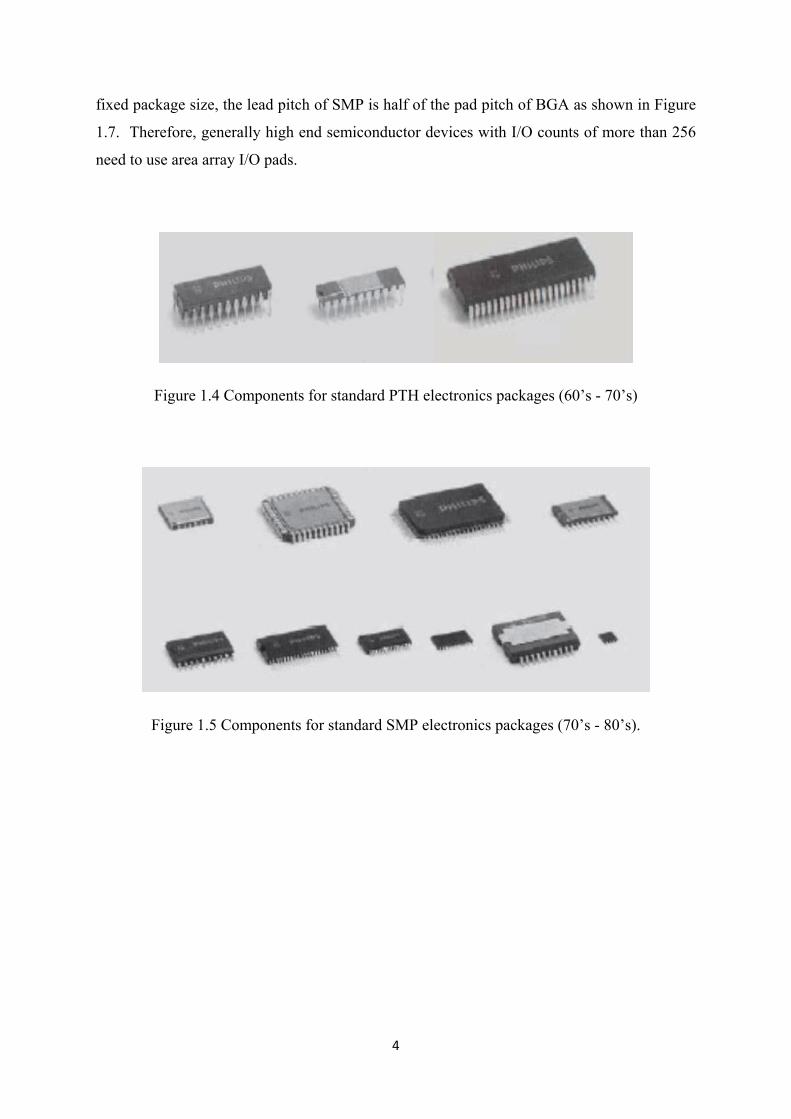
4
fixed package size, the lead pitch of SMP is half of the pad pitch of BGA as shown in Figure
1.7. Therefore, generally high end semiconductor devices with I/O counts of more than 256
need to use area array I/O pads.
Figure 1.4 Components for standard PTH electronics packages (60’s - 70’s)
Figure 1.5 Components for standard SMP electronics packages (70’s - 80’s).
5
Figure 1.6 Left: the structure schematic of a SMP component.
Right: the structure schematic of an area array packaging component.
Figure 1.7 The comparison of pitch distance between SMP and BGA at same packaging size.
At the level between chip and substrate package, the packaging methods also migrated from
Wire Bonded Chips in BGA Carriers (Fig. 1.8) to area array packages (e.g. Flip Chips in
BGA Carriers, Fig. 1.9) to achieve the higher I/O count and smaller size.

6
Figure 1.8 (a) The schematic of wire bond structure.
(b) IBM’s organic BGA carrier built by Endicott interconnect, chips are attached by fine gold
wire bonds.
Figure 1.9 (a) The schematic of flip chip structure.
(b) Intel 90nm Pentium 4 microprocessor in an organic flip chip ball grid array carrier.
In the early 1960’s, IBM first proposed the flip chip technology when the Controlled
Collapse Chip Connection (C4) process was developed. Along with the increase of I/O counts,
higher temperature (e.g. 300 °C) solder bumps (97Pb3Sn) were used in flip chip technology.
To avoid solder joint failures when high temperature solder materials are used, ceramic
carrier with its good CTE match are was adopted in the flip chip package. In order to prevent
moisture, IBM sealed the solder joints with an underfill (Fig. 1.10) composed of an organic
material such as an epoxy or silicone and found that amide-imide underfilled joints can
extend life time up to 10 times longer than the solder joints without underfill [6] [7].

7
Figure 1.10 IBM’s (EI’s) High Performance Chip Carrier (HPCC) [8].
Flip chip packaging has since been widely adopted and used by microelectronics
manufacturers. The typical flip chip integrated circuit is made up of solder joints and
interconnects, and hence the reliability of a flip chip IC mainly depends on the reliabilities of
solder joints and interconnects. Although the dimensions of solder joints and interconnects of
flip chip structure are in the order of microns , their size need to be further reduced to meet
the need of ultra-large-scale integration (ULSI), therefore the reliability of the IC structures
are deteriorating significantly due to the issue of EM. According to the 2003 International
Technology Roadmap for Semiconductors (ITRS) [9], the downsizing trend in flip chip
packaging will continue. Figure 1.11 shows the estimated trend in pad diameter, pad pitch,
line width. The diameter of a solder bump in 2007 was about 50 µm or less [10] and that was
expected to decrease to 20 µm [9]. If a current of 0.2 A passes through a solder bump with a
diameter of 50 µm, the current density is about 104 A/cm2. This current density is high
enough to cause EM damage at a device operation temperature of 100 ºC [2].

8
Figure 1.11 the trend in flip chip package according to ITRS 2003
In addition to the advancement in IC, new packaging methods such as stacked multichip, 3D
packaging, flexible interconnect, multi-layer thin substrate have provided new techniques in
further miniaturization. This means that downsizing trend of electronics devices can be
anticipated to continue and EM is going to become a serious near term challenge for
microelectronics manufacturers.
To reduce the risk of EM failure, one of the methods is to use more EM resistance materials
as interconnect. In the past 40 years, most interconnect conductors for ICs have been
manufactured from aluminium (1-2% Cu may be added to improve its EM resistance [8]).
Nowadays, copper has become an alternative to aluminium as the interconnect conductor in
IC manufacturing. Because relatively less data for copper is available, copper metallization
performance must be examined and discussed.
The geometry and properties of solder joints are very different from that of Al or Cu and EM
in solder joints have also become very important area because much smaller current density is
required to cause EM damage in solder joint than in Al or Cu conductors. Solder alloys have
relatively low melting point and different diffusion pathway compared to Al and Cu and are
sensitive to EM damage [11].

9
1.3 Aims and Objectives of this Research
The aim of this PhD study is to develop a multi-physics modelling methodology for
predicting metal migration for materials in electronic packaging, to understand EM process in
lead-free solder, and to study interconnect designs that reduce failure risk caused by EM. This
will be achieved through the following objectives:
• Review and document state of the art in the theory and computer simulation methods
in atomic migration in metal conductors
• Develop and implement a modeling methodology that couples the effects of electric
current, temperature and its gradient and stress gradient.
• Use computer simulation and experimental methods to help understand EM in thin
film solder materials and solder joints
• Use the computer simulation method to optimize EM-aware designs in
microelectronics devices
• Publish outputs from the work at international conferences and in academic journals.
1.4 Challenges and methodologies
It is now well known that EM is a multi-physics process which involves electrical, thermal
and mechanical effects at the macro scale and at the micro-scale EM is governed by
crystalline structure, lattice defect, grain boundary, free surface and other microstructures.
The root cause(s) are therefore complicated and very challenging to study. The method that is
used in this work is to use computer simulation method to model EM process at the
continuum level, which means that the effects of microstructures are assumed to be taken into
account via material property parameters in the governing equations of EM, which is
basically the equation that describes the diffusion of atomic vacancy in conductors. In the
numerical model, electrical, thermal and mechanical effects are all included and coupled
solutions are obtained. Void formation and evolution are not solved as a coupled phenomena.
Instead, they are modeled using EM simulation results plus a void formation criterion. The
voids that formed are used to modify the model geometry and vacancy distribution in the
altered geometry is solved again. Therefore, void formation and void evolution modelling
includes three phases: vacancy accumulation, void formation and void growth.

10
In the study of EM using experimental methods, one of the problems is that in test specimens,
temperature and/or stress gradients are present which makes analysis of results complicated.
By using thin metal film specimen and copper block as heat sink this problem can be solved.
1.5 Contribution of this Study
The contributions of this work in the area of EM are:
• A truly integrated computer simulation technique which couples all known physical
processes has been implemented and voids formation and growth caused by EM can
be predicted laying a foundation for accurate prediction of EM in complicated
interconnects.
• By using thin films, EM process in a lead free solder has been analyzed without the
effects of thermal and stress so that EM is caused by electric currents only.
• Proposed method of optimizing the design of interconnects so that EM risk can be
reduced.
The results of this research have been presented and published at a number of international
conferences:
• X. Zhu, H. Kotadia, S. Xu, H. Lu, S. H. Mannan, C. Bailey, Y.C. Chan, “Multi-
Physics Computer Simulation of the Electro-migration”, proceedings of the
International Conference on Electronic Packaging Technology & High Density
Packaging (ICEPT-HDP 2011) in Shanghai, China 2011.
• X. Zhu, H. Kotadia, S. Xu, H. Lu, S. H. Mannan, C. Bailey, Y.C. Chan, “Progress in
the Development of an Electro-migration Modeling Methodology”, proceedings of the
10th World Congress on Computational Mechanics (WCCM 2012) in São Paulo,
Brazil 2012.
• Sha Xu, Xiaoxin Zhu, Kotadia, H., Hua Lu; Mannan, S.H.; Bailey, C., Chan, Y.C.,
“Remedies to control electromigration: Effects of CNT doped Sn-Ag-
Cuinterconnects”, proceedings of Electronic Components and Technology Conference
(ECTC) in San Diego, California, 2012.
• X. Zhu, H. Kotadia, S. Xu, H. Lu, S. H. Mannan, C. Bailey, Y.C. Chan, “Modeling
Electro-migration for Microelectronics Design”, International Computational

11
Mechanics Symposium in Kobe, Japan 2012 (JSME-CMD ICMS 2012), key note
paper
• X. Zhu, H. Kotadia, S. Xu, H. Lu, S. H. Mannan, C. Bailey, Y.C. Chan, “Computer
Simulation of Electromigration and Interconnect Failure Prediction”, 2013
International Conference on Electronic Packaging Technology, Daliang, China , 2013.
• X. Zhu, H. Kotadia, S. Xu, H. Lu, S. H. Mannan, C. Bailey, Y.C. Chan,
“Elemctromigration Aware Design for Nano-packaging”, 2013 International
Conference on Nanotechnology, Beijing, China , 2013.
• 2013 R2i2 Electronics Conference: Connecting Research to Industry, Loughborough,
UK 2013
• X. Zhu, H. Lu and C. Bailey, Modelling the Stress Effect During Metal Migration in
Electronic Interconnects, 2014 International Conference on Nanotechnology, Toronto,
Canada , 2014.
Two journal papers have also been published:
• X. Zhu, H. Kotadia, S. Xu, H. Lu, S. H. Mannan, C. Bailey, Y.C. Chan, “Modeling
Electro-migration for Microelectronics Design”, Journal of Computational Science
and Technology, Special Issue on International Computational Mechanics
Symposium 2012, JSME, 2013
• X. Zhu, H. Kotadia, S. Xu, H. Lu, S. H. Mannan, C. Bailey, Y.C. Chan, “Electro-
migration in Sn-Ag Solder Thin Films Under High Current Density”, Thin Solid
Films, ELSEVIER, 2014.
1.6 The structure of the thesis
This thesis consists of 6 chapters. Chapter 1 introduces the EM, the state of the art of
electronic packaging technology, and its reliability issues in terms of EM. This is followed by
a brief introduction of this study and its contributions made in response to the challenges in
this research.
Chapter 2 reviews the relevant literature in aspects of EM and EM modeling respectively.
The EM modeling review introduces the history of numerical methods development in term
of EM and analyzes the contributions, progress and shortage of models.

12
Chapter 3 introduces a EM experiment with thin solder film and its relevatnt analysis. The
experiment aims to explore the EM behavior on a Pb free solder material.
Chapter 4 introduces the mathematical foundations and numerical techniques used in our
model. The EM model procedure involves following parts, diffusion-convection, heat transfer,
stress effect, and electrical effect which are described separately. The mathematical
techniques for implementation and validation are also described and explained. Last, a case
study is demonstrated to show the capablilty of the developed model.
Chapter 5 introduces EM aware design ideas. Relevant modelling analisys are used to
demonstrate the EM aware design methods. A EM aware design rules and standard procssing
are proposed and introduced in this chapter which will greatly help microelectronic designers
to avoid EM damage in their design.
Chapter 6 concludes the whole thesis and introduces the future work of EM modeling.

CHAP
2.1 ove
In this
research
approac
range fr
which r
thermom
reviewe
2.1.1 T
EM wa
topic di
use inte
caused
mechan
form at
Fig. 2.1
2.8 x 10
PTER 2 A
erview of
chapter, th
h work on
ches are dis
from simple
reflect the s
migration (
ed in this ch
The EM Ph
as firstly di
id not arous
egrated circ
by strong
nical stress.
the anode (
1 SEM ima
04 A/cm2 at
A REVIEW
R
f the chap
he phenome
this pheno
scussed in t
e one-dimen
state of the
(TM) and s
hapter.
henomeno
scovered by
se much aca
cuits (IC) c
electric cu
As atoms
(Fig. 2.1).
ages of morp
150 ºC for
W ON ELE
RESEARCH
ter
enon of EM
omenon are
this chapter
nsion to the
art of EM
stressmigrat
on
y the Frenc
ademic inter
commerciall
urrents in m
migrate, vo
phology on
8 days: (a)
du
13
ECTROM
H METHO
M, its impa
e reviewed
r but the foc
e more rece
M modeling.
tion (SM)
ch scientist
rest until 19
ly. EM is a
metal condu
oids form a
n a eutectic S
The hillock
ue to EM [1
MIGRATIO
ODOLOG
act on elec
d. Both exp
cus is on th
ent three-dim
Other atom
and EM aw
t Gerardin o
966 when th
an atomic m
uctors and
at the catho
SnPb solder
k at the anod
0].
ON PHEN
GY
ctrical inter
perimental
he computat
mensional s
mic migratio
ware desig
over 100 y
e electronic
migration p
affected b
ode and ext
r bar due to
de and (b) v
NOMENON
rconnects, a
and compu
tional meth
simulation m
on phenom
gns have al
years ago [1
cs industry b
phenomenon
by temperat
trusions or
EM after a
voids at the
N AND
and past
utational
hods that
methods
mena, i.e.
lso been
12]. The
began to
n that is
ture and
hillocks
applying
cathode

14
It has now been accepted that EM is caused by moment transfer from electrons to atoms. In a
current carrying metal, when an ion is out of its equilibrium position (activated state), it has a
larger effective scattering cross section. Under high current density, the collisions between
electrons and atoms result in significant amount of momentum transfer from electrons to the
ion and the accumulated effect may result in the ion jumping from its lattice point to another
neighboring point, if it happens to be a vacancy. The accumulated effect of this type of event
is the mass transport in conductor that may eventually cause voids at cathode and hillocks at
the anode in the conductor.
2.1.2 The Thermomigration Phenomenon
Thermomigration (TM) is another mass migration phenomenon which is driven by high
temperature gradient. Under a current flow or an external temperature load, the temperature
distribution may not be uniform due to the different thermal absorption and conduction
properties of materials. As a consequence, a large temperature gradient can be built up which
push atoms from high temperature position to low temperature position. In microelectronic
packaging, for example, it is possible that the heat accumulated at the chip side is larger than
that at the substrate side and this may lead to TM due to the different electrical resistances
and thermal capacities of individual parts within the flip chip interconnection structure. Most
time, TM is a byproduct of EM because of the imbalance of joule heating generated at
interconnection and most studies reported that the effect of TM cannot be individually
identified from EM. However, TM can happen even where there is no electrical current.
It has been reported that the initiation of TM in a SnPb solder bump would require a thermal
gradient of 1000-1200 °C /cm, and numerical simulation has demonstrated such a possibility
[13]. Several studies on the TM of Sn-Pb eutectic solder have been reported, where the
apparent segregation of Sn and Pb phases has been confirmed as being due to different
diffusivities [14] [15]. However, to our knowledge, data on the TM behavior of ultra-fine
interconnects (such as nano-interconnects) for some new materials (such as nano-composite
solders and nano-wires/tubes) is lacking, so It is crucial to establish and verify the atomic
migration behavior of TM for such materials.

15
2.1.3 The Stressmigration Phenomenon
The stressmigration is also a mass transport phenomenon which is driven by stress gradient.
In most cases, stress gradient is generated by temperature change in assemblies where there
exists mismatch of the coefficients of thermal expansion (CTE) between dissimilar materials.
It should be noted that the homologous temperatures of Cu, Al and relevant intermetallic
compounds (IMC), such as Cu6Sn5 and Cu3Sn, are low, and hence the interior thermal-
mechanical stresses cannot be effectively released in a short time in the same way as they can
be for the solder which has a high homologous temperature. Stress concentration and cycling
will augment the migration process and cause crack-related failures. SM induced voiding has
long been a standing issue for Cu and Al conductive traces inside the chip [16].
In many numerical studies, hydrostatic stress and hydrostatic stress gradient were used to
calculate the driving force for SM, areas with the most concentrated hydrostatic tensile stress
are thought to be the most probable areas where void nucleates [17] [18]. The relationship
between stress gradients with the locations of the voids was examined using both analytical
and numerical methods [19].The hydrostatic stress, σHS, was defined as the average of σxx, σyy,
σzz: = (2.1)
SM may happen during manufacturing, storage, testing and application period of a product’s
lifecycle but there has been no comprehensive SM study on microelectronic interconnects so
far. However, its potential importance should not be underestimated since the miniaturization
of electronic systems exposes components and interconnects to very high stress gradient
conditions and therefore increases the risk to SM failure. Furthermore, EM itself can create
stress gradient and therefore it is important to study SM in the EM research work.
2.1.4 EM and Conductor Materials
Since this study focuses on the EM issue of microelectronic devices, the interconnecting
structures in integrated circuits and flip chip structure in electronics packaging are the main
concern. Electrically conducting materials which are being used as interconnects are typically
selected based on various factors including their electrical resistivity, thermal conductivity,
EM resistance, thermal stability, adhesion to substrate, and availability of diffusion barriers.
Al is traditionally the most popular metal in IC manufacturing but Cu has become a
replacement of Al. The problem of Cu is that it can diffuse into Si substrates at high

16
temperatures [20]. Due to its higher electrical and thermal conductivity and better EM
resistance than Cu, Ag is also an attractive interconnect candidate [21] [22]. Along with
demonstration of deposition of Ag by evaporation, sputtering and electroplating [23] [24], it
was shown that a sputtered Ag metallization is probably more suitable for ULSI than
sputtered Cu in feature sizes below 50 nm [25]. However, Ag also has some defects to be
used as Ag lacks adequate adhesion to SiO2, [26], diffuses into Si at temperatures higher than
400°C [27] and agglomerates at elevated temperatures [28]. Since 2000, several authers
[20] [29] [30] reported that alloying of interconnect metals with additional elements can
make improvement of EM resistance. Therefore, researches about the effect of solute addition
(i.e., Cu) on the EM behaviour of Ag metallization have been investigated by several groups
[31] [32].
2.1.5 The Effects of Interfacial Chemical Reactions
Although interfacial chemical reactions are not included in atomic migration, interfacial
chemical reactions can speed up the failure process. The local temperature of interconnects
can increase dramatically with the current because of the joule heating phenomenon.
Unfortunately, most microelectronic equipment operates at a temperature about 100 °C, or
even higher in some unanticipated cases. Both internal and external heat may accelerate the
atomic diffusion process, since it is exponentially dependent on the temperature. Thereby, a
fast chemical interaction between solders and substrates can occur, and forms a substantial
amount of intermetallic compound (IMC). Research has confirmed that even current stressing
with a moderate current density could enhance the chemical reactions substantially [33]. It is
known that a thick layer of IMC is both hard and brittle, which has a negative effect on the
mechanical integrity of the interconnection. In particular, the IMC growth and evolution link
with some thermo-mechanical reliability issues due to volumetric shrinkage, Kirkendall void
formation, stress accumulation and the introduction of brittleness [34]. Atomic migration-
induced microstructural evolution in the interconnections, such as phase coarsening, is
another area of concern. However, the chemical reaction processes and their effects on the
reliability of microelectronic interconnects are insufficiently understood as well.
2.1.6 AC or DC?
EM experiments are usually carried out using DC currents. Realistic devices, however, rarely
operate under pure DC conditions and typical interconnect lines are often running with pulsed
17
current (PC), where PC includes both unipolar pulse current (UPC) and bipolar pulse current
or alternating current (BPC or AC). Idle time between pulses can vary between a fraction of a
nanosecond (during peak usage) and hours or even days, during low usage periods. Therefore,
it is important to investigate the EM under AC and PC conditions. In principle, the EM
should not happen under alternating current (AC or BPC) stressing because the net mean
momentum transfer between electrons and atoms is zero over a complete AC period. To
verify this, various models and experiments have been developed to investigate if the EM
exists under symmetric AC stressing. The results are quite different. Boon-Khim Liew [35] in
his work found the EM damage also happen under AC stressing even the frequency was over
1 MHz. The life time in his experiment (Al-2%Si film) under AC stressing is about 1000
longer than the same Al-2%Si film under DC stressing. This result was then confirmed by
various groups but the life time was varying from about 100 to about 10000 longer than DC
condition. The interesting discovery was the sites of void generation in all six
Boon-Khim Liew’s experiments were the middle point between the cathode and the anode as
Fig 2.2 shows [35]. The explanation for the life time of metal under AC stressing is much
longer than the DC condition is easily understood and well accepted that the reverse current
flow drives the backward atomic flux to heal the void then enhance prolongers the lifetime of
metal. But the reason for why EM cannot be eliminated even under very high frequency AC
conditions is still unknown. One possible explanation is the metal microstructure. As the Fig.
2.3 shows, when the atomic flux moves along with the grain boundary, the triple point
structure may block part of atomic flux of specific direction [35]. Another possible
explanation is the oxidation of the pre-void surfaces may prevent the atomic diffusion along
these surfaces and as a consequence a static growth of voids occurs [36]. Also Ki-Don Lee in
his work also concludes that the EM occuring under AC stressing could be results of
combination of thermomigration, back-stress and structure effects [37].

18
Figure 2.2 Photograph of failure site in 800 µm long, 1.2 µm wide, and 0.08 µm thick strip
under pure AC stressing and a SEM of the failure site. AC: J=1.0x10⁷ A/cm2, 25MHz, T=250
ºC [35].
Figure 2.3 In pure AC condition, the void grows during the first half cycle in (a) and
decreases during the opposite current period in (b). As a result, the triple point becomes an
atomic flux blocker for particular direction [35].

19
For determining the mean time to failure (MTTF) of metal under AC conditions, various
groups proposed various models. Ki-Don Lee in his work [37] used 100 kHz - 1.0 MHz AC
stressing at 275 ºC - 325 ºC and found that the EM effect did not fully recover during the
opposite polarity pulse current. The degree of EM recovery in the second half of the AC
period is found to be 70% to 90% of EM effect that developed in the first half of the period.
The MTTF is therefore longer than EM under DC stressing with the same amplitude and the
conductor resistance does not increase linearly with time. Based on this, Ting [38] introduced
a healing coefficient and describes the mean time to failure under AC stressing model as: = ( ∙ ∙( )∙ ) ( ) (2.2)
where r is the duty cycle ratio corresponding to the relative duration of positive and negative
periods, and are current density amplitude during the positive and the negative periods
respectively. Several studies [39] [40] [41] were carried out to determine the values for γ. L.
Doyen and his colleagues [42] expressed the healing coefficient γ as follows: = ∙( ) / (2.3)
The value they obtained for γ is about 0.59 for copper in the temperature range of 25 ºC to
125 ºC.
In Ki-Don Lee’s work [37] the time-averaged current density (Javg) and peak current density
(Jpeak) were introduced (Eq. 2.4 and Eq.2.5). = ( ) (2.4) = ∙ (2.5)
where T is the period of the cycle, J(t) is the time-dependent current density, r is the duty
cycle, and t is time. Figure 2.4 demonstrates several current density waveforms at different
duty cycle (r) and peak current density (Jpeak).

20
Figure 2.4 Current density waveforms at different duty cycles (r) and peak current densities
(Jpeak); for rectangular UPC, Javg = rdc·Jpeak; (a) DC: r = 1, Javg = Jpeak = 1Jo, (b) UPC-1: r =
0.5, Jpeak = 2Jo, Javg = 1Jo, (c) UPC-2: r = 0.25, Jpeak = 4Jo, Javg = 1Jo, (d) BPC: |∫ dt| = |
∫ dt|, Javg = 0 [37] [37].
Several studies have shown that Javg of PC can be treated as effective DC current density in
DC EM model [43] [44] [45]. For example, if Javg values of DC and PC are the same, as
shown in Fig. 2.2 (a)-(c) (where Javg of DC, UPC-1 and UPC-2 = 1Jo), Javg model predicts the
same EM lifetime. Ki-Don Lee in his work [37] also introduced two MTTF models for time-
averaged current density (Javg) and peak current density (Jpeak) respectively as: ∝ ( ( ) )∙ (2.6)
∝ ( ( ) )∙ ∙ (2.7)
where ( ) is the blech’s critical product, which is going to be discussed in the next
section. Ki-Don Lee [37] found that Jpeak model can better predict the short lead UPC EM
lifetime than the Javg model which is more suitable for the DC cases [46] [47] [48], and
concluded that during the off-time between low frequency pulse currents, mechanical back-
stress may reduce the stress gradient built by UPC and increase the EM lifetime of the short
leads.

21
2.2 EM Modelling Approaches
2.2.1 Empirical Approaches of EM Analysis
Since the discovery of EM, much work has been devoted to the understanding of its
mechanisms and impact. For the electronics manufacturing industry, the most important issue
is to control the impact of EM and create designs that will not fail because of EM. In 1967, J.
R. Black proposed the first model that predicts MTTF of electric conductors that are subject
to EM damage. He assumed the MTTF is inversely proportional to the momentum transfer
between thermally activated ions and conducting electrons (Eq. (2.8)): ∝ ∆ (2.8)
where is the density of conducting electrons, ∆ is the momentum transferred from an
electron to an ion, and is the density of thermally activated ions. He further assumed that
both electron density and momentum transfer are proportional to the current density, i.e. ∝ and ∆ ∝ , and the density of activated ions follows Arrhenius law as Eq. (2.9)
[49]. ∝ ( ) (2.9)
where Ea is the activation energy, T is the absolute temperature, and k is the Boltzmann’s
constant, and the mean time to the failure is described as Eq. (2.10) [50] [51]. = ( ) (2.10)
where A is a material and geometry constant. The Black’s equation (Eq. 2.10) is an empirical
model and the parameters therein must be determined by experiments. However, the
theoretical assumptions it assumes are that electron momentum transfer is the root cause of
EM and that atoms in activated state have the greatest chance of receiving momentum from
electrons. The implication of these assumptions is that the EM MTTF is sensitive to current
density, the temperature, and the material properties of the metal. For electronics designers,
these characteristics of EM point to the ways of creating EM-aware designs which will be
discussed later in this thesis.
Four years after Black described his work, J. C. Blair and his colleagues found that in their
experiments that the Black’s model could not fit all experimental results if the current density
exponent is 2 or any other constant [52]. Therefore, the Black’s model was modified to Eq.
22
(2.11) and the current density exponent should be treated as a parameter that is dependent on
material properties and conductor geometry [52]. = ( ) (2.11)
The reported value of n varies for different materials and structures but n=2 is still frequently
quoted in many EM reliability studies and is still being widely used in the electronics
manufacture industry today [53].
In the 1970s, another milestone of EM studying is I. A. Blech’s analysis on the EM in a
simple structure which consists of a short Al strip patterned on a baseline of TiN as shown in
Fig. 2.5 [54] [55] [56] [57] [58]. When an electric current is applied at the TiN baseline, the
electricity flow concentrates in the Al layer due to Al’s lower electrical resistivity. At suitable
current density (2.1 x 10⁸ A/cm2) and temperature (400 ºC) [10], Al atoms migrate from the
cathode to the anode and the consequence of EM can be observed directly as Al strip drift on
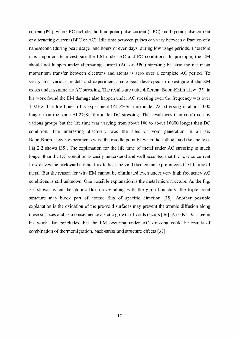
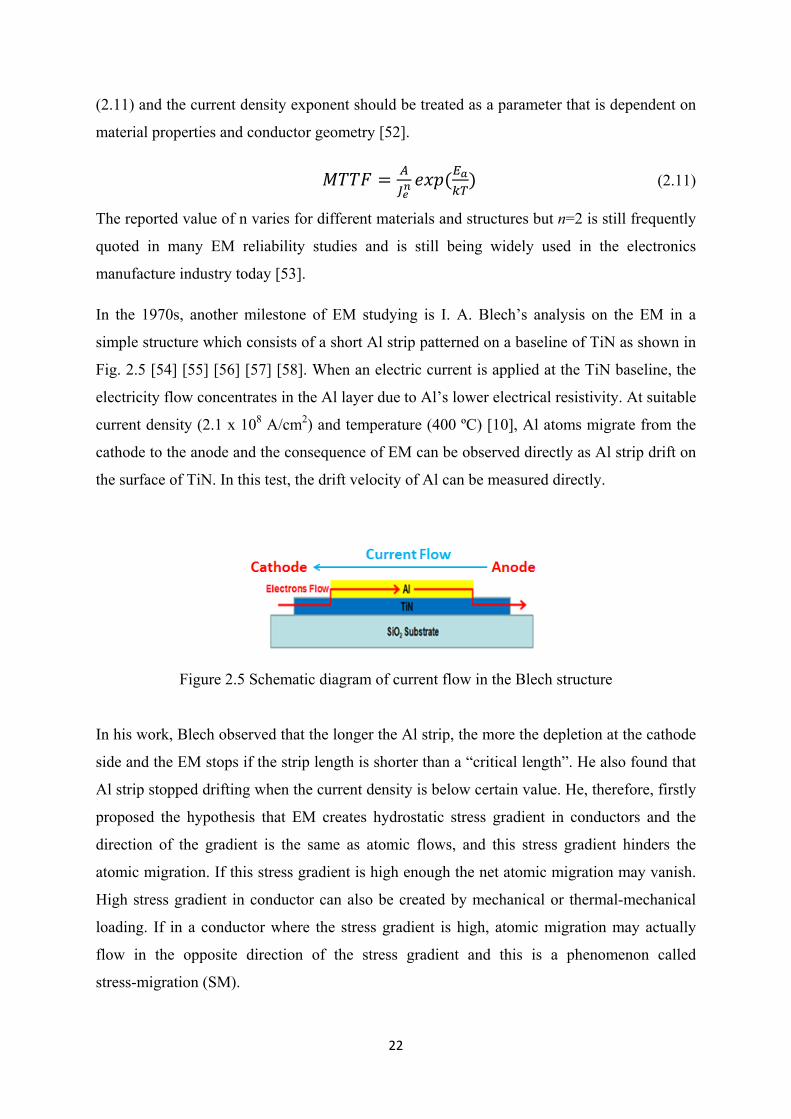
the surface of TiN. In this test, the drift velocity of Al can be measured directly.
Figure 2.5 Schematic diagram of current flow in the Blech structure
In his work, Blech observed that the longer the Al strip, the more the depletion at the cathode
side and the EM stops if the strip length is shorter than a “critical length”. He also found that
Al strip stopped drifting when the current density is below certain value. He, therefore, firstly
proposed the hypothesis that EM creates hydrostatic stress gradient in conductors and the
direction of the gradient is the same as atomic flows, and this stress gradient hinders the
atomic migration. If this stress gradient is high enough the net atomic migration may vanish.
High stress gradient in conductor can also be created by mechanical or thermal-mechanical
loading. If in a conductor where the stress gradient is high, atomic migration may actually
flow in the opposite direction of the stress gradient and this is a phenomenon called
stress-migration (SM).

23
Based on the Huntington and Grone’s work, the electrical force (Fem) of EM is given as
Eq. (2.12) [51]. = ∗ (2.12)
where Z* is the effective charge which represents the sign and the magnitude of the
momentum exchange, e is the elementary charge, E is the electric field. The mechanical force
Fme can be calculated from the gradient of chemical potential in a stressed solid (Eq. 2.13).
Clearly the force is proportional to the negative stress gradient. This means that atoms flow
from high stress region to low stress region under the influence of stress gradient. = − (2.13)
where is the hydrostatic stress, is the atomic volume. In a conductor where EM causes
significant mass migration, stress will develop in regions where atoms accumulate which
results in a stress gradient that is in the same direction as the direction of EM mass flow.
Metals can withstand limited level of stress and this means that stress gradient is dependent
on conductor length—the shorter the conductor length the higher the stress gradient.
Therefore, EM mass migration will be hindered or even stopped by the stress buildup
depending on the length of the conductor and the current density value.
I.A. Blech found that at a “critical length” the mechanical force offsets the electrical force
(Fem+Fme=0) and net mass flow becomes 0. From Eq. 2.12 and 2.13, the critical length can be
described as Eq. 2.14. = ∆∗ (2.14)
where is the critical length of the conductor, and ∆ is the difference between the
maximum downstream stress and the upstream stress. Eq. (2.14) can also be written as Eq.
(2.15). ( ∙ ) = ∆∗ (2.15)
where ( ∙ ) is called the critical product and can be used to define a material’s
resistance to EM damage [57] [58] [51] [59] [60]. The critical product of various materials
have been measured experimentally and used to scale the EM resistance of materials. For
fixed current density, EM stops if the conductor length is shorter than the critical length (and
the conductor becomes ‘immortal’).
Although the Black model and the Blech model are still widely used in the electronics
manufacturing industry for EM-aware designs, these models don’t offer much insight into the

24
EM process and their use is heavily affected by geometric and material factors. For better
understanding of the EM and more accurate lifetime prediction in complicated products,
better analysis methods must be developed so that information such as voids initiation and
growth time and location etc can be predicted.
2.2.2 Numerical Approaches of EM Analysis
EM is a complicated mass transport process that is dominated by current density but also
influenced by thermal and mechanical factors such as the temperature, temperature gradient,
and hydrostatic stress gradient. In mass transport processes where the dominant factor is
temperature gradient or hydrostatic stress gradient rather than current density, the process is
called thermomigration (TM) or stressmigration (SM) respectively. Examples of the study of
TM and SM can be found in Tan and Ye’s works [61] [62] but these two phenomena are not
the focus of this work.
Since EM is a directional atomic/vacancy diffusion under the influence of other physical
mechanisms, it can be described mathematically by a general diffusion equation (Eq. 2.16).
+ ∙ = (2.16a) + ∙ = (2.16b)
where and are the total atomic/vacancy flux vector respectively, and are the
atomic/vacancy concentration, and G is the atom/vacancy generation /annihilation source
term. The atom/vacancy distribution as a function of time can be obtained by solving Eq.
2.16a and 2.16b, if the source term and the expression for atom/vacancy flux are known. It is
worthy to note that the amounts of flux of atoms/vacancy are equivalent but flux direction
were opposite because the atoms movement can actually be considered as a process that the
atoms exchange the position with vacancies directionally as shown in Fig. 1.2. For a specific
problem, if more atoms are leaving than entering in a specific volume, voids will form, grow
and may lead to an open circuit eventually that also mean more vacancies are entering than
leaving in the same volume at the same time. If more atoms are entering than leaving,
extrusions (hillocks) will form and this may lead to short circuits if the extrusions make

25
contact with other conducting parts of the circuit which also equivalent to the process of more
vacancies are leaving than arriving in the same specific volume.
The flux of atomic/vacancy due to pure electrical effect can be expressed rather simply, using
an electrostatic analogue and Einstein's equation for diffusion in a potential field. = | ∗| (2.17a) = | ∗| (2.17b)
Eq. (2.16) and Eq. (2.17) can be combined to give Eq. (2.18).
− ∙ | ∗| = (2.18a) + ∙ | ∗| = (2.18b)
where is the resistivity, and are the diffusion coefficient for the appropriate
atomic/vacancy transport mechanism which can be given by = exp (− ) (2.19a) = exp (− ) (2.19b)
where and are the pre-exponential factor for atom/vacancy diffusivity respectively.
Equation (2.18) shows that EM-induced atomic/vacancy flux is directly proportional to the
current density, to the diffusion coefficient, and to the concentration of diffusing
atoms/vacancies. The vacancy diffusivity is typically calculated from the relation = at the free stress situation [63]. It is worthy noted that atomic diffusivity is dependent
on stress.
2.2.2.1 EM and Mechanical Stress Effect
After Blech had established the theoretical correlation between EM and mechanical stress,
Kirchheim [64], by considering a one dimensional model, added the hydrostatic stress
gradient to the total vacancy flux equation: = − ( − | ∗| + ) (2.20)
where is the diffusivity of vacancy, is the electrical resistivity of conductor, f (0<f<1) is
the vacancy relaxation factor, and is the vacancy volume. Thus, the continuity equation can
be written as

26
= − [− ( − | ∗| + )] − (2.21)
where is the equilibrium vacancy concentration, is the vacancy relaxation time. By
assuming that the volume change is (1 − ) due to the lattice relaxation as a vacancy
replaces an atom [65], Kirchheim described the equilibrium vacancy concentration in a grain
as: = ( ) (2.22)
where is the initial vacancy concentration. In addition, the volumetric strain in a grain
produced by vacancy generation can be described by the Eq. (2.23) [64]. ∆ = (1 − ) ∆ (2.23)
where V is the vacancy volume, ∆ is the volume change caused by vacancy, is the grain
boundary thickness, d is the grain diameter, and ∆ is the generated vacancy concentration.
Thus, the strain rate can be given by: = (1 − ) (2.24)
Based on the Hooke’s law, the relation between deviation of the vacancy concentration from
its equilibrium state and the stressing was established as Eq. (2.25). = (1 − ) (2.25)
where is the appropriate modulus. Equations (2.20) and (2.25) form a non-linear system
which can normally be solved numerically only. Kirchheim did, however, provided analytical
solutions for simple cases [64].
Similar to Kirchheim’s model, Clement [63] proposed a model to establish the relation
between the vacancy concentration and hydrostatic stress as = = (2.26)
where is the change in the volumetric strain due to deposition of atoms at grain boundaries,
is vacancy concentration at lattice site, is a parameter called applicable modulus which
depends on the elastic properties of conductor and adjacent material.
In another way, Sarychev [66] proposed a three-dimensional stress evolution model linked to
EM. In his model, the local volume change is assumed to be generated by vacancy migration

27
and generation due to atomic movement. The local volume change is then treated as an
analog of thermal strain. The stress fields can therefore be calculated as a result of volumetric
strain induced by EM. The volumetric strain is composed of two parts, is the volumetric
strain due to vacancy migration, and is the volumetric strain due to vacancy generation.
They can be described as
= ∙ (2.27) = (1 − ) (2.28)
where is the Kronecker’s symbol, = −( − ) is the vacancy generation rate. Thus,
the combined strain rate due to EM is = + = [ ∙ + (1 − ) ] (2.29)
The total volumetric strain rate due to EM is = [ ∙ + (1 − ) ] (2.30)
By analogy to thermal strain, the volumetric strain caused by the EM can be superimposed
onto the strains tensor with strains due to other loadings. Therefore, the total strain can be
described as = + + (2.31)
where is the total strain tensor, is the strain due to mechanical loading, is
the strain due to thermal load, and is the volumetric strain due to EM.
Compared to Kirchheim’s direct relation between lattice density and hydrostatic stress,
Sarychev’s model employed the idea that diffusion vacancy fluxes give rise to volumetric
strain which can be used to calculate stress fields and therefore to establish the relation
between ‘Back stress’ effect and EM was widely accepted and supported by various groups
such as Povirk [67], Rzepka [68], and Garikipati [69].
2.2.2.2 EM and Thermal Effect
Generally speaking, the temperature is determined by heat source in the environment, joule
heating in conductors, and the thermal conductivity of the materials. If joule heating is the
only heat source, the governing heat transfer equation can be described as Eq. (2.32) [70]. ( − ) = · ( ) (2.32)

28
where is the material density, is specific heat capacity, is joule heating rate, and
is the thermal conductivity.
As mentioned previously, temperature is a very important factor in EM process, as in other
activated processes that obey the Arrhenius laws. H. B. Huntington [71] found that one of the
driving forces in atomic migration is the temperature gradient and this driving force can be
written as Eq. (2.33). = ∗ (2.33)
where is the temperature gradient driving force, ∗ is the heat of transport, T and are
absolute temperature and temperature gradient respectively. Therefore, the total
atomic/vacancy flux equation that include the contribution from self-diffusion, electric
current, hydrostatic stress gradient, and temperature gradient can be described as: = − ( + | ∗| + ∗ − ) (2.34a) = − ( − | ∗| − ∗ + ) (2.34b)
where the drift velocity of EM, TM, SM can be defined as: = | ∗| (2.35a) = ∗
(2.35b)
= − (2.35c)
2.2.2.3 Generation /Annihilation Term
Vacancies in conductors can be generated and annihilated. In 1971, R. Rosenberg and
M. Ohring [72], proposed a one-dimensional continuity vacancy flux model that included a
vacancy generation/annihilation term: = − | ∗| − (2.36)
where the equilibrium vacancy density is defined in Eq. (2.20) by Kirchheim [73] [74].
It means that vacancies are annihilated if the vacancy concentration is greater than the
equilibrium value, or vacancies are produced if the vacancy concentration is less than the
equilibrium value. Substituting the Eq. (2.22) into the Eq. (2.36), the vacancy
generation/annihilation term is given by:

29
= − ( ) (2.37)
where c is the normalized vacancy concentration defined as c = Cv/Cvo.
Unlike the empirical models mentioned in 2.2.1, the vacancy flux based mathematical model
can take into account multiple physical processes and address the root cause of EM. In
principle, if material property parameters are known, vacancy distribution and evolution can
be solved numerically for given boundary and initial conditions. Since the multiple physical
processes are involved, the vacancy flux governing equation has to be solved numerically and
make a separate analysis for individual effect possible.
2.2.2.4 Void Nucleation
Vacancies are defects at atomic scale and voids in conductors that may lead to significant
damage to electric circuits. Many researchers support the hypothesis that void nucleation was
caused by the accumulation of vacancies at sites of vacancy flux divergence caused by EM. It
is believed that voids form when the vacancy concentration reaches a critical value [75] [76]
[74] [77] [78] [79] [80] [81]. However, R. Rosenberg [82] and W. D. Nix [83] reported that
in some cases an unrealistically high vacancy concentration is needed to trigger void
formation. Meanwhile, several research studies attempted to establish a relation between void
nucleation and mechanical stress by investigating the impact of mechanical stress on void
formation under various conditions [84] [85] [86] [87]. Gleixner and Nix [88] in their model
used hydrostatic stress as a metric for void growth but Kircheim [73] used the von-Misses
equivalent stress instead. Argon and et al. [89] combined the hydrostatic stress and von-
Misses stress to a new “de-cohesion critical stress” to describe void nucleation. The stress
criteria for void nucleation are still being discussed [73] [90] [91] [92] [93]. In addition,
several authors [94] [95] [96] [93] reported that voids may also form at pre-existing free
surfaces which could be resulted from contamination during fabrication stage. For example,
by assuming that a circular flaw of radius Rp is present in a volume (Fig. 2.6), Finn [94]
proposed the critical stress for void nucleation is given by Eq. (2.38a). = (2.38a)
where is the surface free energy of the metal. Clements and et al. [95] then reported the
void may extend beyond the flaw area and the critical stress is correlative with the void area
and then modified the equation to:
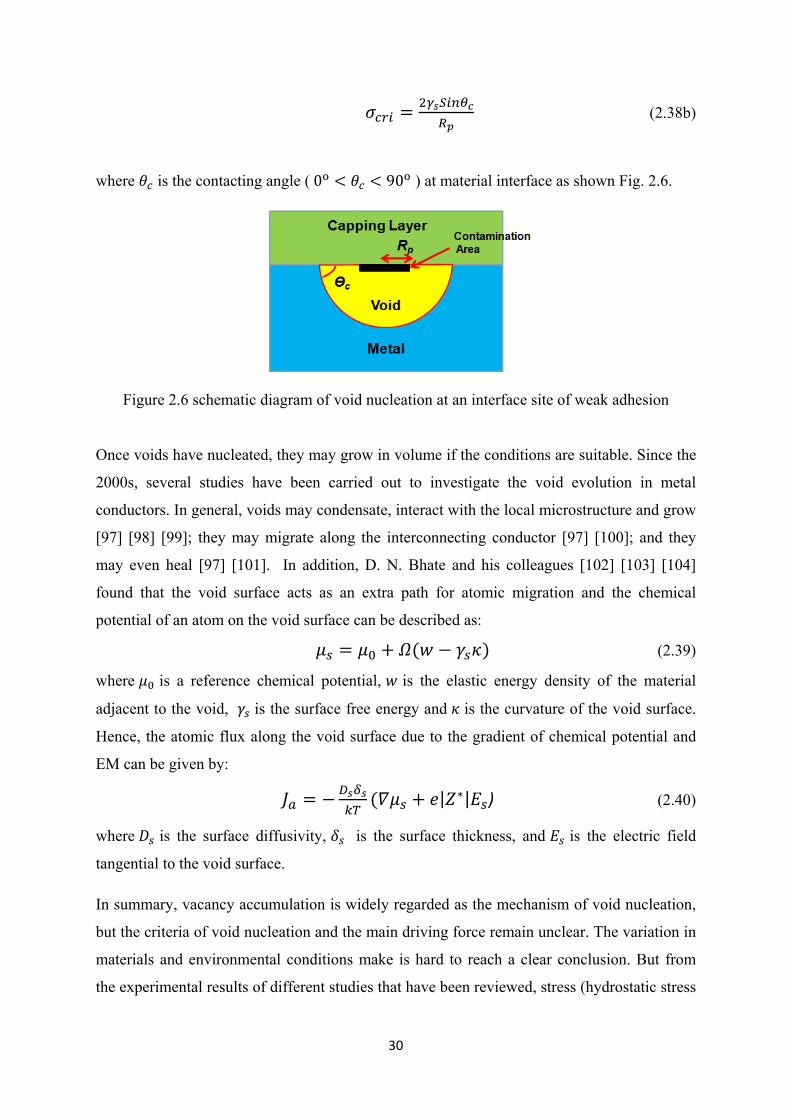
30
= (2.38b)
where is the contacting angle ( 0 < < 90 ) at material interface as shown Fig. 2.6.
Figure 2.6 schematic diagram of void nucleation at an interface site of weak adhesion
Once voids have nucleated, they may grow in volume if the conditions are suitable. Since the
2000s, several studies have been carried out to investigate the void evolution in metal
conductors. In general, voids may condensate, interact with the local microstructure and grow
[97] [98] [99]; they may migrate along the interconnecting conductor [97] [100]; and they
may even heal [97] [101]. In addition, D. N. Bhate and his colleagues [102] [103] [104]
found that the void surface acts as an extra path for atomic migration and the chemical
potential of an atom on the void surface can be described as: = + ( − ) (2.39)
where is a reference chemical potential, is the elastic energy density of the material
adjacent to the void, is the surface free energy and is the curvature of the void surface.
Hence, the atomic flux along the void surface due to the gradient of chemical potential and
EM can be given by: = − ( + | ∗| ) (2.40)
where is the surface diffusivity, is the surface thickness, and is the electric field
tangential to the void surface.
In summary, vacancy accumulation is widely regarded as the mechanism of void nucleation,
but the criteria of void nucleation and the main driving force remain unclear. The variation in
materials and environmental conditions make is hard to reach a clear conclusion. But from
the experimental results of different studies that have been reviewed, stress (hydrostatic stress

31
or von-Misses equivalent stress) criteria could be used more suitable to situations where the
stress is mainly caused by external forces and the vacancy concentration criteria should be
used where void nucleation is caused by several driving forces. Clements and several authors’
boundary condition on the other hand is more suitable to describe the special case where
there are pre-flaw areas in the sample, which is in fact a common situation in electronics
manufacturing [94] [95] [96] [93]. In our modelling work, the current density, stress and
vacancy concentration were used as the criteria of void nucleation and will be discussed in
section 4.3.4.
2.2.2.5 Damage Mechanics/Measurement
It’s important that the onset of EM damage can be described by some measurable or
calculable parameters in EM analysis. Since the 1960s, various studies were carried out to
measure the extent of EM damage. In laboratory tests and in applications, EM damage can be
defined according to the total void area, variation in ultrasonic wave propagation speed,
change in electrical conductivity, thermal resistance ratio, variation of density and etc. [105]
[106] [107] [108] [109] [110]. In earlier numerical analysis, plastic strain, plastic strain rate
or the energy have been used as primary damage metrics in EM damage analysis [111] [112]
[113] [114] [115] [116] [117] [118]. However, Dasgupta and et al. [119] in their work
demonstrated that the maximum plastic strain can localize at different location in the material
which may not match the site of void nucleation. Meanwhile, Solomon and Tolksdorf [120]
proved that the dissipated energy is not a reliable damage metric in the issue of EM.
Based on Valanis’s theory on “Entropy State”, C. Basaran [121] [122] and his colleagues
linked the extent of EM damage to the different degree of “disorder” in current carrying
conductor. This disorder can be described as a macroscopic measure of the number of ways
atoms can move in a given volume. Thus the greater the entropy, the more ways atoms can
move from their original position and the more severe the material degradation. The
relationship between the disorder and the entropy is given by: = (2.41)
where s is the entropy of system, W is the disorder parameter which gives the number of
micro states corresponding to given macro state. The relationship between entropy per unit
mass and the disorder parameters can be given by:

32
= = (2.42)
where R is the universal gas constant, is specific mass, and N0 is the Avogadro’s constant.
Eq. (2.42) can be rearranged as: = (2.43)
With the disorder parameter expression as the Eq. (2.43), the ratio of change in disorder
parameter can be used as degradation metric by the following relationship: = ∆ = (1 − ) (2.44)
where D is the damage parameter which varies from 0 (no damage) to 1 (complete damage) is
a scalar value used to map degradation of the conductor, is the damage criteron. More
information about derivation and experimental validation of this entropy model can be found
in [123] [124] [125] [126] [127] [128] [129] [130] [13] [131]. Entropy production during EM
process is given as: ∆ = ( : + : + : ) (2.45)
where : is joule heating generated entropy, : is mass diffusion produced
entropy, : is the viscoplastic deformation produced entropy. Rearrange Eq. (2.44) and
Eq. (2.45), the damage parameter evolution can be expressed as:
= (1 − ( : : : ) ) (2.46)
More details about parameter determination, special condition discussion and the relationship
between the damage parameter and the mechanic stress can be found in the papers by
Basaran et al [132].
Since EM has been discovered, how to measure/standardise the damage of EM is an open
question. The area of voids and electrical resistance change are two most widely accepted
methods. However these two values are typically not useful for measuring EM at the initial
stage, because these two values show no change for a long time as the directional movement
of vacancies has not condensed to voids. C. Basaran’s ‘disorder’ theory proposed a new
measurement for EM intensity which can also reflect the intensity of vacancy movement
rather than only void formation. The ‘disorder’ as a metric could be more accurate for EM
measurement but we have to note that the implement of ‘disorder’ in experiment is not as
easy and direct as measurement of electrical resistance and voids area for EM study.

33
2.2.2.6 Molecular Dynamics Model
EM can be studied at the atomic level using molecular dynamics (MD) and other atomistic
modeling methods [133] [134]. An example of this type of work is the study of EM failure
on Aluminium grain boundary by Tsutomu Shinzawa, and Toshiyuki Ohta in 1998 [135]. In
their work, the grain boundary diffusion for Al interconnection and the atomic motion near
the grain boundary were investigated and accurately calculated by using embedded atom
method (EAM). The potential energy Ei for one atom (j) is described as: = (∑ ) + ∑ (2.47) where F is embedding function, is the electron density contributed by atom (j), is two
body pair potential. To trace grain boundary diffusivity, they assumed grain boundary
structure with total 774 Al atoms in which 264 atoms are fixed at the both end and 510 atoms
are diffusible as shown in Fig. 2.7. To trace grain boundary diffusivity, mean-square
displacement (MSD) are descried as: = ∑ [ ( ) − (0)] (2.48)
where is number of atoms in the grain boundary region whose width is assmed to be 10A, and ( ) is i-th atom position at time t. then the diffusivity for grain boundary is given by: = → (2.49) Figures 2.8 shows the trace of atomic trajectories at temperature 700K when tensile strain in
y-direction is kept 2%. It is shown that the free atoms are restricted only near the grain
boundary. Tsutomu Shinzawa, and Toshiyuki Ohta [135] also verified that the atoms
diffusion is almost linearly proportional to the temperature and diffusion time and the grain
boundary diffusivity is highly dependent on the grain boundary structure.
A similar work was introduced by Mehmet Kadri Aydinol and his colleague to investigate the
wind force of EM on Al interconnects using non-equilibrium molecular dynamics (NEMD)
[136]. The EM wind force was calculated based on a theory using the pseudo-potential
formalism of the elements. For this purpose, some impurities were introduced into free atoms
of a structure which is quite similar as Fig. 2.8 to generate pseudo-potential which is

34
dependent on the type and distribution of the imperfections in the lattice. It was found that the
electromigration force on the impurity depends on the scattering power of the atom, which is
related to the chemical valence. They calculated the atomic jump frequency of aluminum
atoms in alloys containing impurity elements like Cu, Mg, Mn, Na, Sn and Ti. It was found
that the EM diffusion process was slowed down considerably, compared to pure Al, in alloys
containing elements Cu, Mn and Sn.
Figure 2.7 Grain boundary structure, 264 fixed atoms, 510 free and 9 layers stacked in z-
direction [135].

35
Figure 2.8. Trace of atomic trajectory where any atoms that move beyond inter atomic
distance between nearest neighbors [135].
2.2.3 EM Modelling Methodologies
The methodologies of EM modeling have been developing along with the construction of EM
theory. The atomic/vacancy flux models based on Eqs. (2.16) and (2.26) have been solved
using numerical techniques by many researchers to evaluate in details the influence of
temperature, stress, and geometry on EM and the techniques are still being developed and
improved. Most EM models are based on Finite Element Analysis (FEA) method, which is
used to calculate the basic physical quantities such as current density, temperature, and stress
etc. A simple example of using FEA in EM analysis is to use FEA to predict current density
distribution and then use Black’s equation to predtict conductor life-time. For example, C. C.
Yeh Everett and his colleagues [137], used this approach to analyze the current distribution
and life-time of solder bumps; and similarly Hieu and Salm [138] used current density
distribution to predict the failure location and the lifetime in the solder joint. While in these
examples only the electric currents were solved using FEA, in order to solve the

36
atomic/vacancy diffusion equation, multi-physics FEA techniques have to be used, which
will be discussed in following sections.
2.2.3.1 Atoms/Vacancies Condensation at Boundary
Considering a specific volume, passing through of a continuous steady state atoms/vacancies
flow does not result in EM damage because the atom/vacancy density does not change in
considering volume [10]. The vacancy left by atomic movement will be covered by following
atoms of atomic flow. Thus the EM damage only appearance when the atom/vacancy density
changes in the considering volume. That is to say the EM only happens when the divergence
of atomic/vacancy flux in a specific volume is non-zero. Such situation normally occurs at
material boundaries and grain boundaries. For example, at the interface between silicon (Si)
and aluminum (Al), the diffusion of Al atoms or vacancies from Si is negligible and vice
versa. When electrons enter Al from Si, the Al atoms that are displaced won’t have Al atoms
to replace them, and this causes accumulation of vacancy in Al. Conversely, extrusions will
be generated where the electrons are entering the Si from Al. Therefore, the studies for how
to handle the boundary and interface are crucial for EM modeling and will discuss in this
section.
Shatzkes and Lloyd were the first that rigorously derived the relation between the divergence
of vacancy flux at material boundary and interconnect lifetime [75]. In their 1D model, they
considered electrical effect only and assumed the influence of EM and diffusion only on the
vacancy flux, the continuity Eq. (11) along their 1D model can be written as: = − | ∗| (2.50)
where the source term G=0 was used. A semi-infinite line was assumed in their model as Fig.
2.9 under the boundary conditions:
(−∞, ) = (2.51) (0, ) = 0 (2.52)
which means that the vacancy concentration at x=−∞ is fixed at an initial equilibrium value
, and the material boundary is a perfect blocking boundary for vacancy flux. The solution
of Eq. (2.50) at the blocking boundary is given by Laplace transformation [75]. ( , ) = 1 + + 2[ (1 + ) + √ exp(− )] (2.53)

37
where = | ∗| (2.54)
Assuming that the failure criterion is when the vacancy concentration reaches a given critical
value Cvf significantly higher than the initial equilibrium value Cv0, and that β ≫ 0, then Eq.
(2.53) is approximated [75] by ≈ 4 = (| ∗| ) (2.55)
where is the time the vacancy concentration reaches the given critical value Cvf.
Substituting Eq. (2.19) into (2.55), the mean time to failure can be described as: = exp ( ) (2.56)
which is similar to the Black’s Eq. (2.11). It means, if considering the void nucleation is the
result of vacancy concentration reaches a given critical value, the mean time for failure is
proportional to the inverse square of current density.
Figure 2.9 the semi-infinite grain boundary proposed by Shatzkes and Llyod.
Kirchheim and Kaeber [74] proposed a new model of a finite line with blocking boundary
conditions at both ends of the line as:
(0, ) = (− , ) = 0 (2.57)
where L is the line length, so that the solution becomes:
( , ) = − ∑ (− + ∝ )∞ (2.58)
where = | ∗| (2.59)
They also provided the analytic solution which is determined by the term A0

38
= ( ) exp (2.60)
And = [ ( ) ( )( ) + (2.61) = + /4 (2.62)
With the = 3.4 and parameters in the Table 2.1, The results of the two boundary conditions
(semi-blocking and both end blocking) are compared in Fig (2.10).
Parameter Value
Dv0 0.052cm2/s
Ea 0.9eV
1.69x10⁻⁶Ω cm
Z* -5.0
Je 2 MA/cm2
L 100
T 573K
Table 2.1 parameters used in the calculations.
Figure 2.10 Vacancy concentration at the blocking boundary at x=0 for the semi-infinite line,
and the finite-line.

39
Figure (2.11) shows the vacancy concentration along the finite line at different times. This
analytic solution for a finite line has been used in this work to verify the numerical model that
is discussed in chapter 4.
Figure 2.11 Vacancy concentration along the line at different time according to De Groot
SR’s analytic solution [139]
From the Fig. 2.10, it can be seen that the solution for semi-infinite line and finite line agree
well for early two minutes and significantly deviate after. This is because there is a vacancy
concentration gradient developing in finite line which counters the vacancies drift when
vacancies drift from the anode to the cathode, As a result, the net vacancy flux is gradually
reduced to zero to reach the steady-state condition given by Eq. (2.58). However, the ten
minutes it took to reach vacancy saturation is a very short time compared to the typical failure
time of several hours) that has been observed in experiments. It is worthy to note that
Rosenberg and Ohring [72] in their modeling work also observed such a short time to reach
the steady-state condition. Their EM model also used Eq. (2.50) but included a source term: = − (2.63)
Substituting to the Eq. (2.50): = − | ∗| − (2.64)

40
Based on their experimental observations that the damage site caused by EM were generally
related to the site of significant change in the grain size [75], Rosenberg and Ohring built a
1D atomic/vacancy flux EM model in which they considered the intersection of two grains
forming a grain boundary (Fig. 2.12) [140]. Each grain can be characterized by their
respective vacancy diffusivity Dv, the activation energy Ea, and the equilibrium vacancy
concentration Cv. Based on this assumption, vacancy flux divergence can occur at the grain
boundary. At steady-state ( / = 0), the vacancy concentration and the flux are
continuous along the grain boundary interface: ( = 0) = ( = 0) (2.64)
And ( = 0) = ( = 0) (2.65)
Therefore, the solution of Eq. (2.64) for each grain [140]: (x) = ( ) = (0) exp(− ) , < 0 (2.66) (x) = ( ) = (0) exp(− ) , < 0 (2.67)
Where (0) is the vacancy saturation at x=0, given by (0) = [ | ∗| − 1] (2.68)
And = − | ∗| − [ | ∗| + ] / (2.69) = − | ∗| − [ | ∗| + ] / (2.70)
With their work, the vacancy saturation along the grain for different vacancy relaxation time
can be calculated.
Figure 2.12 Model of two grain boundaries intersecting at x=0.

41
However, the aforementioned models are based on the assumption that the cross section area
of conductor is constant and current density is evenly distributed throughout the length, thus
the temperature along the length is also constant that unintentionally eliminates the thermal
and stress effect. Therefore, the time scale to reach the vacancy saturation from these three
models is too short and the maximum vacancy saturation is very low.
2.2.3.2 Atomic/Vacancy Flux Divergence Based Analysis
Based on the atomic/vacancy flux equation Eq. (2.34), Dalleau and Weide-Zaage [141]
considered that the electrical resistivity of conductor is temperature dependent as = (1 +( − )), where is the temperature coefficient, and substituted Eq. (2.19b) into (2.34)
then derived the approximate atom/vacancy flux divergence (A/VFD) equations for the
respective driving forces: ( ) = ( − + ) ∙ | ∗| ∙ (2.71) ( ) = − + ∙ − ∗ ∙ + ∗ (− )
(2.72) ( ) = − ∙ ∙ + ( ) − −+ ( ) − (2.73)
where E is Young modulus, v is the Poisson ratio, , is the expansion coefficient of the
metallization.
Since the lifetime of a metal line is closely related to the void and hillock formation, the
A/VFD can determine the rate of void growth rate and therefore predict the lifetime. Dalleau
and Weide-Zaage used 3D coupled thermal and mechanical analysis for EM analysis [78].
They initially ran electrical-themal analysis to predict current density and temperature, and
the result of the analysis was then used as input for the thermo-mechanical analysis to
calculate hydrostatic stress. The results were then used to calculate the atomic flux
divergence. In their subsequent work, the method was also applied to real cases such as a
dual-damascene structure [142] [141]. Similarly, in 1999, Rzepka et al. proposed their 3D
EM model for interconnecting metal lines based on FEA [143]. In their work, they considered
surface tension due to the changes in surface curvature as one of the driving forces. By using

42
the thermal analysis routine of the commercial FEM software package ANSYS, all the
driving forces were calculated sequentially. Lee et al. [144] modeled both the heat flow and
the current density in a solder bump to explore the relation between the combined effects of
these two factors on the atomic flux. Liu et al. [145] used ANSYS and a separate diffusion-
convection equation solver to calculate the divergence of atomic vacancy caused by electric,
thermal, and stress effects to predict intensity of EM, and similarly, Cacho and his colleagues
used COMSOL in their work to solve the divergence of atomic vacancy and concluded that
the intensity of mechanical effect is as strong as the EM [146]. Li linked ANSYS and Matlab
to calculate the atomic/vacancy flux divergence [147]. He obtained the distribution of
temperature, current density, hydrostatic stress from ANSYS and calculated the atomic flux
divergence in Matlab which can complement the limitation of ANSYS and thus atomic flux
divergence can be calculated directly.
However, Tan and et al. in their work analyzed and validated the A/VFD method and found
that the two assumptions on which the A/VFD method is based on may make results
inaccurate [148]. Therefore, they discussed the assumptions and improved the A/VFD
method. Firstly, they pointed out that the thermal and stress part of A/VFD (Eqs. (2.72) and
(2.73)) are derived based on the energy balance equation: + − ( ) = 0 (2.74)
where Kfilm and kdie are the thermal conductivity of the metallic film and the dielectrics
respectively, Tfilm and Ts are the temperatures of the metallic film and the substrate, tfilm and
hdie are the thickness of metallic film and dielectrics respectively. The individual terms of this
energy balance equation stand for Joule heating due to electrical current, lateral heat
conduction along the plane of the film and vertical heat conduction through the dielectrics
into the substrate respectively. However, the third term was considered too small and
discarded in the derivations of Eqs. (2.72) and (2.73). Tan and his colleagues then used a
simple model of Cu film with different thicknesses to explore the significance of the third
term as shown in Table 2.2. The results show the vertical heat conduction through the
dielectrics into the substrate could be more important than the joule heating effect and in-
plane heat conduction.

43
Line Thickness
(µm)
First Term
( /μ )
Second
Term( /μ )
Third Term
( /μ )
Contribution by
third term of
energy balance
equation (%)
3 3.46x10⁶ 3.26x10⁶ 0.2x10⁶ 6.1
1 3.46x10⁶ 2.84x10⁶ 0.62x10⁶ 17.9
0.325 3.46x10⁶ 1.56x10⁶ 1.9x10⁶ 54.9
0.2 3.46x10⁶ 0.36x10⁶ 3.1x10⁶ 89.6
Table 2.2 The contribution of the three terms in energy balance equation (Assuming the
substrate thickness is 300 µm and current density is 1MA/cm2)
Moreover, in the derivation of Eq. (2.73), the relationship between the hydrostatic stress and
the temperature change is considered and expressed as: = ( + + ) = − ∆( ) ( − ) (2.75)
where is the stress-free temperature of the interconnect and ∆ is the difference of the
CTE between the interconnect metallization and the surrounding materials. Eq. (2.74) was
derived by assuming that the cross section of the metal film is an elongated ellipsoid.
However, Tan and et al. pointed out that the stress distribution is highly dependent on the
structure geometry and in most real cases are rectangular rather than ellipsoid and therefore,
the two assumptions may affect the accuracy of the A/VFD method when A/VFD is applied
to narrow interconnects. In their work, Tan pointed out that the divergence of the respective
atomic/vacancy fluxes can be derived based on the Green’s theorem [149] [150] [151]
without the above-mentioned assumptions: ( ) = ( − + ) ∙ | ∗| ∙ ∙ (− ) (2.76)
( ) = − ∙ − ∗ ∙ ∙ − − ∗ − ∙ ( )
(2.77)
( ) = − ∙ ∙ − ∙ + ∙ − ∙( ) (2.78)

44
Compared to the conventional A/VFD method, the new A/VFD method overcomes the
drawbacks stated above. The vertical heat conduction, geometry factor and the directions of
the respective driving forces are taken into account. Tan et al. also verified the new A/VFD
method in their subsequent work with a reservoir interconnect structures and proved the new
A/VFD method is more realistic than conventional A/VFD method [152].
2.2.3.2 Voids Formation and Evolution Simulation
The challenge of structure lifetime prediction is to predict the time, location and growth rate
of voids. One of FEA based methods is to calculate the distribution of A/VFD in each
element. This method requires the knowledge of the lifetime and proper time steps are
assigned to each iteration, and the element volumes are changed according to the atomic
volume changes that have been predicted by the A/VFD method. The model proposed by
Dalleau and Tan simulated the void formation by physically deleting elements [153] [141]
[142] [143] [154]. Sasagawa in his work then reported the smaller size of elements used in
this type of analysis gives more realistic results [154] [155] [156]. Therefore, he added a
procedure that changes the thickness of each element according to decreased volume of
atomic flux divergence at the end of iteration calculation.
In the work of Sasagawa and et al. [155] [156], the criterion was either when the temperature
exceeds the melting point of the metal due to Joule heating along with the decrease of lines’
width, or the thickness of the elements becomes smaller than a pre-defined threshold value.
In their work, they determined effective width at 2x10⁻³ times the initial thickness of line
based on their experimental measurement and successfully predicted the lifetime of test
structure. The Dalleau’s work used a different threshold for void formation [78] [79] [142].
They considered element to be a void when the atomic concentration reaches 10% of the
initial concentration (C/C0) and proposed a function f which can be used to correlate with the
lifetime as: = (2.79)
where f is a function of various physical parameters. Based on the pre-defined criterion (C/C0
≤ 10%) and specific function f, the lifetime can be obtained. Although the aforementioned
two void growth simulation methodologies have good accuracy to simulate the void growth
location and void shape, the structure lifetime prediction for these three simulations was not

45
so successful because the two criterion, however, have not been theoretically proved.
Therefore the lifetime prediction in the issue of EM is still a big challenge.
2.2.3.3 Other Void Simulation Methods
Level Set Method (LSM) is a numerical method that can be used to track the shape of
surfaces and interfaces [157] [158] [159]. It has been applied for topography simulations in
microelectronics simulation. In the case of EM, it has been used by several authors to
simulate the void shape evolution [157] [159] [159] [160] [161] [162] [163] [164]. Khenner
et al. proposed a level set formulation for two-dimensional grain boundary grooving due to
surface diffusion driven by EM and local curvature gradients [161] [165]. Based on
Khenner’s work, Nathan et al. [162] carried out analytical approach for drift velocity of EM
as: = (− ) (2.80)
and reported that the calculated drift velocity were highly consistent with the experimental
results. Using a similar approach Averbuch et al. [166] proposed another level set numerical
approach for surface velocity with considering curvature gradients and electrical effect: = ( − | ∗| ) (2.81)
where Ds is the surface diffusivity, is the surface thickness, is the surface free energy, is the curvature of the void surface, and is the surface component of the current density.
Based on Eq. (2.74), the finite difference discretization on a regular grid and a second-order
Runge Kutta time integration scheme [167] [161] [168] [163] was used for several initial void
shapes like elliptic, triangular, and square voids and found that under weak electric field a
random initial shape becomes circular and the void migrates along with the electric field and
under strong electric field the circular void becomes unstable and transform to slit-like shapes.
These results were in highly agreement with Xia’s work [169].
In addition, several EM models [170] [171] [172] [173]that are based on the Phase Field
method [174] were also reported to study on EM-induced stress evolution or failure
mechanism.
2.3 Conclusion

46
In this chapter, we reviewed EM phenomenon, its mechanism and some relevant factors
which may affect mass migration. We also reviewed and discussed various EM modelling
methodologies from early empirical ones to modern numerical ones in chronological order.
Literature review is a very important part of my modelling work which helps me understand
the mechanism of EM better. Many creative thoughts I got from previous EM studies inspired
me and also deeply affected my EM modelling work.

47
CHAPTER 3: EM IN THIN SOLDER FILM
3.1 Introduction
The aim of this chapter is to investigate EM behaviour in a solder material using
experimental observation and computer modelling.
As mentioned in Chapter 1, in flip chip technology, solder joints are used to attach
semiconductor chips to substrates or printed circuit boards. The solder joints are both
mechanical support of the assembly and electrical interconnects. The flip chip technology is
now widely used in advanced electronic products because it produces smaller packages, and
faster devices than, for example, wire bonding. However, a potential drawback of using
solder is that solder materials usually have worse EM resistance compared to copper,
aluminium, gold and other conductors that are also widely used in microelectronics
manufacturing. This is mainly due to its low melting point and its diffusion pathway.
Currently, each solder bump of flip chip structure carries an electric current of about
0.2 A-0.4 A, while the diameter of solder bumps is about 50 µm or less. This is believed to be
very close to solder alloys’ carrying capability. As the trend of further reduction in the size of
solder bump continues, the current density in solder bumps will increase to values of in
excess of 104 A/cm2 [10], which is considered to be a critical level for EM damage to occur
in solder. Therefore, EM is becoming an increasingly important reliability issue in flip chip
solder joints manufacturing and design.
Traditionally, eutectic SnPb or other lead containing solder alloys are used in manufacturing
but they have largely been replaced by lead-free solders because of the concern for the impact
of the toxicity of lead. Among all the lead-free solder candidates, SnAgCu and SnAg are two
of the most popular ones in the industry. Although a considerable amount of research has
been carried out to study the property and performance of Pb-free solders [10] [11], lead-free
solder is still not as well-understood as Pb containing solders simply because the latter have
been used and studied for several decades. The work described here is intended to contribute
to the understanding of EM process in lead-free solders by exploiting computer simulation
which was carried out by the University of Greenwich and experimental work which was
carried out by the King’s College, London.

48
In most studies of EM, particularly in those where high current densities are used, cannot
avoid rapid temperature increase due to joule heating. This means that the process is a
coupled TM and SM - Electromigration phenomenon and this complicates the analysis and is
not helpful in understanding EM. To reduce the effect of TM and SM, an ultra-thin film
structure has been used in our experiment based on two considerations. First, a structure with
a small crossing-sectional area to make the current density high enough is needed and the
structure should be able to cool down fast the raised temperature caused by joule heating.
Second, when TM and SM effect have been de-coupled, the EM damaging process will be
significantly prolonged. In ultra-thin structure it is easier to observe the EM damage with
such conditions.
To reduce the temperature even further, a heat sink with large mass was used to allow heat to
be dissipated rapidly from thin lead-free solder film and to keep temperatures constant so
that decoupling TM and SM from EM can be achieved [175] [176]. In the present work, large
temperature rises and thermal gradients are avoided by utilizing both thin film and large
thermal mass as heat sink. Computational simulation of the coupled thermal–electrical
problem confirmed that the effect of TM had been eliminated almost completely in this study.
3.2 Experimental Details
The set-up of the experiment consists of a thin film strip (average thickness 600 nm) of SnAg
alloy on a piece of glass, which in turn is mounted on a copper plate. Fig. 3.1 (a) shows a plan
view of the test set-up while Fig. 1 (b) shows a schematic cross section of the samples used.
The procedure of preparing the samples is as follows. Firstly, a Cr adhesion film with 5 ± 1
nm thickness is coated on a 150 µm thick glass cover slip using an evaporation technique (U-
300 Oerlikon) in vacuum (10-5 mbar). Next, a nominally (as measured by the evaporator) 305
± 5 nm thick eutectic Sn-Ag solder is deposited on top of the Cr using the same technique.
The 305 µm wide, 5 mm long solder strip geometry (long enough to eliminate back stress
effects on EM) was created by using a glass mask during the evaporation deposition process.
Next, the anode and cathode were connected by wires to the electrical instrumentation using
silver loaded epoxy adhesives so as not to disturb the delicate thin film on the glass substrate.
The approximate dimensions of the Ag loaded adhesive interconnects are 4 mm by 4 mm by
4mm each and they are placed away from the solder strip so as not to interfere with the
current flow patterns in the strip. Two sets of samples are connected in parallel to the power
supply; one was kept at room temperature (15 ± 2 °C) while the other is on a hotplate that is

heated
samples
the resi
increase
evidenc
Microsc
accelera
(AFM)
3.3 Exp
The sur
3.2 (a).
the roug
arise. A
then ex
shows t
separati
associat
partial c
to a tempe
s. The resis
istance incr
e indefinite
ce of EM da
copy (SEM
ating voltag
in tapping m
Figure
perimenta
rface profile
Apparently
ghness of t
As-prepared
amined by
the cross-se
ion betwee
ted with the
coalescence
rature of 3
stance of the
reases by 1
ely, solder
amage wou
M) using an
ge, and usin
mode using
3.1 (a) Plan
al Results
e of a specim
y, a random
the surface.
films were
SEM. The e
ection imag
n Ag and
e high hom
e of the thin
5 °C. Initia
e solder stri
10% from i
at the cath
uld be destro
n FEI Qua
ng a Bruker
g a Si tip.
n view of sp
men was an
m element h
It is expec
cross-sectio
evaporated
ge which in
Sn phases
ologous tem
n film and th
49
ally, a volta
rips is moni
its initial v
hode side o
oyed. Samp
antaFEG S
(ex-Veeco)
pecimen geo
nalysed usin
has been int
cted that lo
oned using
film had an
ndicates tha
. It is beli
mperature o
he formation
age of 740
itored and th
value. If th
of the sold
ples were ex
SEM in ba
) Caliber SP
ometry and
ng AFM an
troduced in
ocal concent
the ion bea
n average th
at the film
ieved that
of the Sn du
n of isolated
mV is app
he experim
he resistanc
der strip w
xamined by
ackscatter m
PM Atomic
(b) electrica
d the result
nto the expe
tration in cu
am milling t
hickness of 6
is amorpho
the roughn
uring deposi
d grains.
plied in bot
ment is termi
ce were allo
would melt
y Scanning E
mode with
c Force Mic
al setup
ts are shown
eriment resu
current dens
technique [1
636nm. Fig
ous and the
ness of the
ition, which
th set of
inated if
owed to
and the
Electron
20 kV
croscope
n in Fig.
ulting in
sity may
177] and
g. 3.2 (b)
ere is no
film is
h allows

Figure
In the c
was 85.
116 mA
densitie
Because
resistan
explain
cathode
transmi
The so
imperfe
to insist
the curr
cathode
3.2 (a) AFM
case of the r
.6 mA, whi
A. This is c
es in the s
e of the low
nce to rise b
ed by void
e to the ano
itted light th
older film t
ection of the
t on making
rent distribu
e’s bottom c
(a)
M image of
room tempe
ile for samp
caused by th
solder strip
wer current
by 10% wh
d formation
ode [178].
hrough the f
that is sho
e mask that
g more sym
ution asymm
corner.
sample topo
rature samp
ple 2, which
he specime
s, therefore
density and
hereas it too
in the sold
The distrib
film, and thi
own in Fig
is used in th
mmetric samp
metric so tha
50
ography and
section.
ple, i.e. sam
h was heate
en’s geomet
e, are 4.41
d lower tem
ok only 367
der strip ca
bution of v
is is shown
g. 3.3 is no
he sample p
ples becaus
at an unamb
d (b) SEM i
mple 1, the m
ed to 35 °C,
try variation
×104 and
mperature in
7 h for case
aused by EM
voids is mo
in Fig. (3) f
ot symmetr
preparation
se the asymm
biguous cur
(b)
image of so
measured ini
exhibited a
ns. The init
5.98×10⁴ A
n case 1, it
e 2. The res
M as atoms
ost clearly s
for sample
ric. This w
process. No
metry is of
rrent density
)
older thin fil
itial electric
an initial cu
tial average
A/cm2 respe
took 983 h
sistance rise
s migrate f
seen by loo
1.
was caused
o attempt w
interest as i
y peak occu
lm cross
c current
urrent of
e current
ectively.
h for the
e can be
from the
oking at
by the
was made
it makes
urs at the

51
=
Figure 3.3 Void distribution of sample 1 observed optically in transmission where the sample
is represented by the dark area and voids by the bright spots
The same sample is examined using SEM and the images are shown in Fig. 3.4. As expected,
it shows that voids formed at the cathode and hillocks formed at the anode . This is consistent
with EM theory that attributes the phenomenon to the effect of momentum transfer from
electrons to atoms [10]. Because of the asymmetric cathode geometry of the sample, the
maximum current density occurs at the bottom corner of the cathode and as voids in this
region form, the maximum current density location moves upwards (and diagonally initially)
accordingly. Away from the current density peaks, there are also zones of voids located
upwind and downwind from the central vertical strip and on the anode side, there is also a
pronounced hillock in the sharp bottom corner where there is an abrupt change in the current
density, and other hillocks scattered throughout the region. The hillocks bear a remarkable
similarity to tin whiskers as observed by K.S. Kim and et al. [179] [14], probably due to the
same underlying cause, i.e. a stress build-up in the bottom solder layers causing the
whisker/hillock to grow [10]. EDX analysis of the hillocks shows an absence of Ag. The
similarity to tin whiskers would also seem to prove that the atoms are carried within the bulk
of the solder rather than at the top surface of the solder, where atomic transport might have
been thought to be easier. The presence of an oxide layer on top of the solder may be
responsible for this.

Fig
botto
im
The opt
the cath
that the
they are
microst
again a
corners
gure 3.4 SEM
om). The sm
mage. The sc
tical transm
hode region
e latter two
e genuinely
tructure mig
a highly vo
but is less
M images o
mall red circ
cale bars in t
mission imag
as expected
arise from
y due to EM
ght have he
oided region
s distinct th
f sample 1 a
cle in the top
the microgr
r
ges of samp
d, but also s
imperfectio
M cannot be
lped voids
n, and a lin
han in samp
52
at increasin
p left image
raphs from t
respectively
ple 2 are sh
some in the
ons in the o
ruled out b
formation.
ne of voids
ple 1. Again
ngly higher m
e is shown m
top down ar
y.
hown in Fig
centre and
original film
because the
The sharp
s appears to
n, there are
magnificatio
magnified in
re 200, 20 a
. 3.5. Again
anode regio
m although
roughness
upper corne
o run diago
regions of
on scale (to
n the bottom
and 10 micr
n, voids are
ons. It is con
the possibi
of the film
er of the ca
onally betw
f voids upw
op to
m left
ons
e seen in
nsidered
ility that
m and the
athode is
ween the
wind and

53
downwind of the diagonal void line and, a hillock forms at the location of maximum current
density.
Figure 3.5 Void and hillock distribution of sample 2 that are observed a) optically and b) by
SEM
3.4 Coupled Electrical and Thermal Analysis
Temperature is a very important factor in EM analysis. In order to understand the temperature
distribution in the sample, 3D Finite Element analysis using the software package ANSYS
12.0 has been used for the thermal analysis of the thin film tests as described above. In Fig.
3.6 the model geometry and boundary conditions are shown. The Joule heat generation in the
solder strip, the losses of heat through air and the glass to the copper block have been taken
into account by using appropriate loading and boundary conditions. Fig 3.7 shows the FEA
mesh of the model. The material properties that have been used in the analysis are listed in
Table 3.1. The distribution of the temperature in sample 1 is shown in Fig. 3.8 and 3.9. The
predicted maximum temperature rise is 0.356 °C and 0.454 °C for sample 1 and sample 2
respectively. The maximum in-plane temperature gradient is 0.04 °C/cm. In this model, the
solder layer thickness is very small compared to other geometric dimensions (such as the
thickness of the copper block) of the model, the mesh resolution in the out-of-plane is not

54
high enough to compute the temperature gradient in that direction. Such low temperature
gradient level is confirmed by K.N.Tu and et al. [14] that TM effects can be ignored in this
experimental setup because the temperature gradient threshold value for TM is about of
1000 °C/cm.
The equivalent thermal simulation has also been carried out on a multi-physics software
package PHYSICA [180]; the results from PHYSICA are highly consistent with the results
from ANSYS. Because of low temperature gradient throughout the specimen, the stress
gradient from thermal expansion can also be considered as being de-coupled from the EM
phenomenon as well.
Figure 3.6 the geometry of FEA model and the boundary conditions.

55
Figure 3.7 Mesh condition of simulation
Given Parameters Values Ref.
Solder Strip Dimensions: L:5 mm / W:305 µm / T: 636 nm measured
Glass Dimensions: L:22 mm / W:22 mm / T: 150 µm measured
Copper Dimensions: L:125 mm / W:40 mm / T: 5 mm measured
Applied Voltage: 0.74 V measured
Current: 85.6 mA measured
Solder Thermal Conductivity:
Glass Thermal Conductivity:
50 W/(m.K)
0.96 W/(m.K)
[49]
Copper Thermal Conductivity:
Ambient Temperature:
Convection Coefficient:
400 W/(m.K)
15 °C
10 W/(m2.K)
[49]
Estimated
Estimated
Solder and Glass Emissivity: 0.94 [49]
Copper Emissivity: 1 [79]

Gap bet
Ther
betw
Figur
substra
F
tween the c
the glass su
rmal Condu
ween coppe
re 3.8 Temp
ate and glas
Figure 3.9 T
opper block
ubstrate:
uctance of ga
er and glass
Tab
perature dist
s slide for s
Temperature
k and
ap
:
ble 3.1 Param
tribution (°C
sample 1; th
edg
e (Unit: °C)
56
2.5×1
meters for t
C) from a 3D
he light blue
ge of glass s
) distribution
0.1 µm
05 W/(m2.K
thermal anal
D model, w
e line locate
lide.
n for solder
K)
lysis
which includ
d in the cen
r film only f
Est
Est
ded solder, c
ntre of mode
for sample 1
timated
timated
copper
el is the
1.

57
3.5 Evolution of Voids
Many authors have studied the link between the magnitude of current density and void
formation in EM, and the consensus is that in general the higher the current density, the
quicker voids form if other conditions are the same [10] [175] [181] [182]. In this work, void
evolution has been analysed using modelled current density distribution in solder film.
PHYSICA was used because it is relatively easy to implement the user routines on this
platform for the analysis.
Sample 1 has been used for the starting geometry in the computer simulations. When a 0.74V
bias was applied to the electrodes, maximum current crowding was observed at the bottom
corner position, which is thus the most likely site for the presence of the first voids to form.
The exact mechanism for void formation will depend on the microstructure of the thin film.
However, this is initially uniform across the sample and hence if void formation occurs
preferentially in one location over another, this relative probability depends on the local
current density and hence geometrical factors alone. When a void forms, the site of maximum
current crowding moves, most likely, to adjacent elements where the next voids are expected
to form. After the calculation of the current density distribution, the two elements with the
highest current density (and hence the highest atomic flux according to Eq. (2.16a) and
Eq. (2.34a)) were removed and then the current density distribution was re-calculated to
capture the effect of void evolution on the distribution.
The results showed that the elements with the highest current density always appears on the
top right corner of the growing void as shown in Fig. 3.10. By repeating the above mentioned
procedure of element removal and the current density distribution recalculation a number of
times, a diagonal line of voids formed. Experimental observation as shown in Fig. 3.10
shows that while such a line does form up to a distance of 50 microns in the experiment, it
does not continue to the edge of the strip. Instead the line of voids appears to curve back
towards the anode for 50 microns and then continue vertically upwards. Other voids also
form on both sides of this central line. This indicates that other mechanisms must come in to
play in order to explain these findings, and it is postulated in the next section that thermal
gradients, though small, may also play a role.

58
Figure 3.10 (a) Initial current density distribution (Unit: MA/m2). (b) Current density distributions. The void has a size of two elements. (c) Current density distributions. The void has a size of eight elements. (d) Current density distributions. The void has a size of eighteen
elements.
The void nucleation and evolution process appears to be very similar to that described by
Meyer MA and et al. [183]. During void evolution (the period from the formation of the first
void formed until the circuit opens), the highest current density and resistance increased
linearly followed by a sharp rise towards the end, matching the fourth stage as described by S.
W. Liang and et al. [182] as Fig. 3.11 and 3.12 show. The resistance matches the
experimentally observed rise of 10% when 80% of the contact is open, in rough agreement
with Fig. 3.4.

Fig
3.6 Di
The ato
tempera
[184] [1
changes
gure 3.11 H
ivergence
omic flux ve
ature gradie
185] [153]
s of atomic
Highest curre
Figure 3.1
of Atomi
ector is a co
ent and hyd
[186]. The
concentrati
ent density
12 Resistanc
c Flux
ombination
drostatic str
divergence
ion.
59
as number o
ce changes
of contribu
ress gradien
e of the ato
of removed
as void gro
utions from
nt as shown
mic flux is
/dead eleme
ws in size.
self-diffusio
n in Eqs. (
an indicati
ents increas
on, electric
(2.16a) and
ion of the l
sed.
current,
d (2.34a)
localised

60
Simulation work was carried out for mimicking atomic migration with the atomic flux
calculated from Eq. (2.34a). Assuming that all thermal gradients and hydro-static stress
gradient can be ignored in the experiment, Eq. (2.16a) and (2.34a) reduce to:
+ ∙ − + | ∗| =r (3.1)
For a given gradient in distribution, the atomic flux in the solder can be calculated. If there
is no source of vacancy, the divergence of this flux is responsible for the depletion or
accumulation of vacancy and therefore is the cause of the creation of voids and hillocks in
solder. By using the parameters listed in Table 3.2, the atomic flux of the electrical
component at the corner site is calculated and shown in Fig. (3.13). The atomic flux
divergence can be written as Eq. (3.2). Without considering the direct force of EM (the term
related to gradient of Ca), the divergences of atomic flux ( ) contributed by electrical part
can be written as Eq. (3.3) and the simulation results are depicted in Fig. (3.14).
( ) = − ∗ − ∙ + ∗ − ∙ (3.2)
( ) = − ∗ − ∙ (3.3)
Parameters Value Reference
Dimension As Table I measured
Temperature 15 °C / 35 °C measured
D0 (Initial Diffusivity) 0.027 m2/s [145]
Ea (activation energy) 0.8 eV [145]
Z (Effective Charge) -40 [145]
ρ (Resistivity) 3.35×10⁻⁷ Ωm (Sample 1)
/ 2.47×10⁻⁷ (Sample 2)
Ωm
measured
Table 3.2 Parameters for diffusion-convection model

Based o
at time
value al
Fi
on the resul
2.0x10⁶ sec
lso appears
Figure 3.1
gure 3.14 T
lts shown in
conds (556 h
s at the tip o
3 Atomic fl
The divergen
n Fig. 3.15,
hours) is 0.0
of the void.
61
flux distribu
nce of atom
the maximu
0548 and th
. If Ca = 20
utions aroun
mic flux at tim
um normali
he element w
% is assum
nd the void.
me 556 hou
ized diverge
with this ma
med to be th
urs.
ence of atom
aximum div
he criterion
mic flux
vergence
for void

formati
sensitiv
predicti
measure
3.7 EM
It shoul
current
by an a
fluxes c
excess v
region,
gradien
was mo
A/cm3.
A/cm3 i
role in p
on, voids w
ve to the a
ion of voi
ements.
M and Curr
ld also be
density [17
additional c
contributed
vacancy con
and is th
nt of the cur
odelled and
However,
is negligibl
present wor
will form a
activation e
id formatio
rent Dens
noted that
75] in the pr
current den
d by current
ncentration
he force wh
rrent density
the highest
K.N.Tu and
le [175], th
rk.
at around 2
energy Ea
on relies o
sity Gradie
several aut
resence of s
nsity gradien
t density an
in the high
hich drives
y [182]. In
t current de
d et al. con
herefore cur
= +
62
2000 hours
and diffus
on accuracy
ent
thors have
severe curre
nt term in
nd current
h current cro
the excess
n this work,
ensity gradi
ncluded that
rrent density
=
s. However
ivity an
y of activ
reported vo
ent crowdin
Eq. (3.4) w
density gra
owding regi
s vacancies
the current
ient has bee
t the curren
y gradients
(− ∗ ) +
r, void gro
nd therefor
ation energ
oid formatio
ng, and this
where, an
adient respe
on relative
to diffuse
t density gr
en found to
nt density g
are expect
+ ∆
owth rate is
re accuracy
gy and dif
on in areas
has been ex
nd are
ectively, ∆to the const
in the dire
radient (Fig
o be about 1
gradient bel
ted to play
s highly
y of the
ffusivity
s of low
xplained
vacancy
is the
tant flux
ection of
. (3.15))
1.81x10⁶
low 1010
a lesser
(3.4)

63
Figure 3.15 Current density gradient distributions
3.8 Conclusion
In this chapter, an experiment regarding EM was introduced. A very thin (600nm) Pb-free
solder film has been manufactured for investigating the pure electrical effect of EM
behaviour in the Pb-free solder. The experiment was designed in such a way that temperature
gradient and stress can be ignored. The film is very thin and therefore the out of plane stress
is negligible. By using ANSYS and PHYSICA, this experiment design was proved a success
also with regards to the temperature gradient effect on EM. A transparent glass substrate was
used the solder film and in this novel way, voids can be observed on both sides and the voids
evolution process had been checked and recorded by using SEM, AFM and electrical
resistance measurement regularly. Under a high current density stressing 6×10⁴ A/cm2, voids
appear at around 983 hours and the experiment was stopped when the electrical resistance
increased by 10% to avoid the specimen being burnt and evidence of EM destroyed. The first
voids appeared at the highest current density area and new voids basically appeared at the
new maximum current density area. Some voids formed at the middle of the specimen and it
can be explained by the existence of defects. A full current density analysis was used to
explain the void growth history. It was found that the appearance of the initial voids matched
what is expected but the voids evolution at a later stage does not match simulation result.
Other methods have been tried to address issue. For example, instead of using a critical
current density as the void formation criteria, critical current density gradient has been used
but no conclusive results have been obtained. Further experiments are therefore needed and
are being carried out by City University of Hong Kong.

64
CHAPTER 4: MULTI-PHYSICS MODEL DEVELOPMENT
AND IMPLEMENTATION
4.1 Introduction
EM process is a multi-physics process that involves electric conduction, heat transfer,
mechanical stress, and diffusions of atoms and voids. Therefore, numerical models should
include those physical processes in order to describe EM correctly. In this chapter, the EM
governing equations, the numerical solution techniques, and the implementation of them in a
multi-physics software package are presented.
4.2 Modelling Methodology
The physical processes that are present in EM are more often than not dependent on each
other. Attempt to analyse these processes is bound to be innacurate. In the computer
simulation research work that has been done to date by many researchers, not all of the
physical processes have been taken into account and this makes it difficult to compare the
simulation results with experimental results. In this chapter, a closely coupled multi-physics
modelling method has been proposed. It can be used to predict atomic/vacancy concentration
and void formation in metals where EM is affected by electrical, thermal, stress, and
geometry factors.
The method is outlined in the flow chart in Fig. 4.1. It describes the way EM is modelled
seamlessly, from electric current prediction to void formation. The model has been
implemented using the multi-physics software package PHYSICA [187], which is capable of
solving fluid flow, heat transfer, electric field and current distribution and general diffusion
equations simultaneously. In the following, the relevant mathematic foundation of
PHYSICA modules is described.
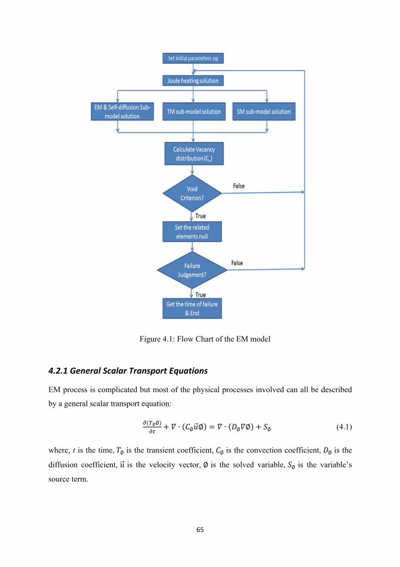
65
Figure 4.1: Flow Chart of the EM model
4.2.1 General Scalar Transport Equations
EM process is complicated but most of the physical processes involved can all be described
by a general scalar transport equation:
( ∅∅) + ∙ ( ∅ ∅) = ∙ ( ∅ ∅) + ∅ (4.1)
where, t is the time, ∅ is the transient coefficient, ∅ is the convection coefficient, ∅ is the
diffusion coefficient, is the velocity vector, ∅ is the solved variable, ∅ is the variable’s
source term.

66
4.2.2 Electric current and joule heating
Because the current density is the main driving force of EM, the current density calculation
must be included in this EM model. The relationship between the current density and the
electric field is = (4.2)
where is material conductivity, and can be calculated from electric potential ∅ as: = − (∅ ) (4.3)
Electromagnetic fields are governed by Maxwell’s equations [188]. In this work, only steady
state conduction is considered and the governing equation is the Laplace equation (Eq. 4.4) ∅ = ∅ = 0 (4.4)
This is a special case of the general equation (4.1).
4.2.3 Heat transfer
Temperature gradient affects atomic diffusion in solids and therefore affects EM. The
gradient can be obtained by solving the temperature distribution. The governing equation for
heat transfer is similar partial differential equation as general scalar transport equation (Eq.
4.1):
( ) + ∙ ( ℎ) = ∙ ( ℎ) + (4.5)
where h is the enthalpy and ℎ = and is the specific heat, is the density, is the
thermal conductivity. In EM analysis, the main heat source is joule heat generated in
conductors. Therefore, the heat source Sh can be written as:
= | | (4.6)
Thermal conduction in conducting metal occurs in solid and therefore the difference of
convection term can be ignored
67
4.2.4 Structural Mechanics Module
Another driving force for EM is the mechanical stress gradient which is typically generated
as the results of temperature change and the mismatch of thermal expansion coefficients of
two or more different materials. Stress is a second order tensor. Because it has six
independent components as Fig. 4.2, and in engineering it is often written as a pseudo vector:
Figure 4.2 Components of stress = ( ) (4.7)
Stress tensor satisfied the following equilibrium equation.
+ + + = 0 (4.8)
+ + + = 0 (4.9)
+ + + = 0 (4.10) = = = (4.11)

68
where bx, by and bz are body force components (such as gravity) per unit volume. Stress
components are not independent variables and therefore the above equations cannot be solved
directly. Stress is caused by deformation which is described by strain. Strain ε is a tensor but
it can be expressed as a pseudo vector which is defined in Eq. (4.12).
+++=
∈∈∈ (4.12)
In isotropic solids, the stress and strain vectors are linked by the following constitutive
relationship = (4.13)
where
[ ] = ( )( )1 − 0 0 01 − 0 0 01 − 0 0 00 0 0 0 00 0 0 0 00 0 0 0 0
(4.14)
and E and ν are the Young’s modulus and Poisson’s ratio respectively.
Eqs. (4.8)-(4.11) result in a set of partial differential equations with the displacement
components (u,v,w) as the independent variables [189] and they can be solved using Finite
Element method.
In EM analysis , hydrostatic stress and its gradient are used to calculate a driving force that is
caused by stress effect of EM ( Eqs. (2.34a) and (2.34b)), local regions where the highest
concentrated hydrostatic tensile stresses are located have been found to be the most probable
areas where voids nucleate [17] [190]. The hydrostatic stress is defined as the mean of the
three normal stress components as Eq. (2.1).
69
4.3 Implementation
In Chapter 2, Eqs. (2.16) and (2.34) show that the governing equation for atomic/vacancy
evolution is a form of the general scalar transport equation which includes “convection”
terms. Convection is usually caused by fluid flow. In a conductor, there is no real fluid flow
and this is therefore not a real diffusion-convection phenomenon in a single phase fluid. The
“velocity” is actually the drift velocity that is caused by the current density, temperature
gradient and the stress gradient. Interconnects in microelectronics are often made of more
than one materials. For example, aluminium/copper lines may be joined with titanium and
solder alloys are bonded to copper metallization. This means that the material constants in
Eq. (2.16) are not the same everywhere and drift velocity varies from one conductor to
another even in a 1D model. This means that some boundary conditions need to be changed
in PHYSICA.
The solution procedure has been implemented in PHYSICA as follows:
1. Apply voltage boundary condition to the model and solve for electric potential and
current density in the whole model. This is done in the PHYSICA’s Magneto
Hydrodynamics Module [187].
2. Apply thermal boundary conditions to the model, use Joule heat density that is
obtained from electric modelling as a heat source to calculate the temperature
distribution of the model. Thermal Transfer Module [187].
3. Apply mechanical boundary conditions and use the temperature obtained in the
thermal solution to predict stress and its gradient in the model. Structural Mechanics
Module [187] is used.
4. Code PHYSICA and make it be able to calculate drift velocity distribution (Eq.
(2.34)) and solve Eq. (2.16) to obtain vacancy distribution. Scalar module [187] is
used for this step.
5. Carry out voids evolution simulation if required. User routines [187] are used for this
calculation.
6. Repeat from step one for the next time step until the required time is reached, or if a
failure criteria is met.

70
4.3.1 One Dimensional Model with Pure Electrical Effect
The modeling started from the simplest scenario (electrical effect only) and a one
dimensional analysis was used. EM is assumed as a process controlled by a vacancy diffusion
mechanism, in which the diffusion takes place by vacancies switching lattice sites with
adjacent atoms. The relevant governing equations therefore are Eq. (2.16b) and (2.34b)
without the thermal and stress term which can be described as: = − ( − | ∗| ) (4.15)
A 100 µm long Al line with constant cross-section area was used in this analysis and the
computational domain was divided into 50 elements along the length. An electric potential
difference was applied at the two ends of the domain generating a uniform electric filed and a
constant current density. A block boundary condition for diffusion is assumed at both ends of
the conductor and the diffusion flux is zero at the ends. Fig. 4.3 shows the model
schematically. The EM drift velocity was calculated as 0.116 µm/s if the electric current and
the parameters in Table 4.1 are used. The vacancy concentration was defined and coded into
PHYSICA and normalized vacancy concentration (C=Cv/Cv0) distributions at time 10s, 100s
and 800s were calculated and shown in Fig. 4.4. The results were compared to an analytic
solution derived by R.L. de Orio and his colleagues [49] and the simulation results are
identical to the analytical results as described previously in section 2.2.3.1.
Figure 4.3 The schematic diagram of boundary conditions.
Parameter Value Reference

71
Dv0 0.052cm2/s [145]
Ea 0.9eV [146]
Z* -5.0 [146] ρ 1.69x10⁻⁶Ωcm [145]
E 69 Gpa [145]
v 0.33 [145]
f 0.6 [145]
Ω 1.66x10⁻²³ unit/cm3 [145]
J 2MA/cm2 -
T 573K -
Table 4.1 Parameters used in the calculations
Figure 4.4 The normalized vacancy concentration distribution in (a) graph and (b) contour at time: 10s, 100s, and 800s.
4.3.2 Back Stress Effect
Back stress in EM is caused by changes in atomic concentration. As atomic concentration
changed it gives rise to volume strain. As back stress develops, its gradient then generates an
atomic flux which is opposite to the original atomic flux that is caused by electric current.
The volumetric strain caused by EM can be treated in the same way as thermal strains but the
temperature change in thermal strain calculation is replaced by a measure of the change in
atomic concentration, which is determined by flux divergence. The stress field therefore can

72
be calculated as the result of volumetric strain which directly links to the divergence of
vacancy flux. All components of a stress tensor can be calculated and thus hydrostatic stress
is calculable. The vacancy flux with contribution from stress gradient can be described as: = − ( − | ∗| + ) (4.16)
The EM model is based on the assumption that the vacancies switch their site with atoms.
The vacancies’ relaxed volume is smaller than the atomic volume. Then at a grain boundary
or at a dislocation, a local volumetric strain can occur because of this change in volume.
Since diffusion-convection is a time dependent process, the volumetric strain rate can be
described as:
= ∙ (4.17)
where EMijε
is the volumetric strain due to vacancy flux divergence, ijδ is the Kroncker’s
symbol. By analogy to thermal strain, the volumetric strain caused by the EM is coded into
PHYSICA and superimposed onto the strains tensor with strain due to other possible loadings,
thus the total strain can be given by:
EMij
thermalij
mechij
totalij εεεε ++= (4.18)
where totalijε
represents the total strain tensor, mechijε
is the strain due to mechanical loading,
thermalijε
is the strain due to thermal loading.
For a confined metal Al line, for example the Al line covered by a heavy passivation layer as
Fig. 4.3 shows, the displacements at w direction are greatly restricted. Therefore, the strain at
w direction is assumed to be zero.
According to Eq. (4.12), the standard strains ( ijε) can be described as:
x
ux ∂
∂=ε , x
vy ∂
∂=ε , x
wz ∂
∂=ε (4.19)
x
v
y
uxy ∂
∂+∂∂=γ , x
w
z
uxz ∂
∂+∂∂=γ , x
w
z
uxz ∂
∂+∂∂=γ (4.20)

73
In the confined Al line, 0=== yxxzz γγε
, By using the strain-stress constitutive relationship
of Eq. (4.13) and (4.14) the total strain loading of Eq. (4.18) can be formulated as:
3)]([
1 em
zyxx TvE
εασσσε +Δ++−= (4.21)
3)]([
1 em
zxyy TvE
εασσσε +Δ++−= (4.22)
3)]([
1 em
yxzz TvE
εασσσε +Δ++−= (4.23)
where
03
)]([1 =+Δ++−=
em
yxzz TvE
εασσσε (4.24)
where E is young’s modulus, v is Poisson’s ratio, α is the coefficient of thermal expansion.
Thus the all components of the stress tensor ( xσ , yσ, zσ ) can be calculated as:
+Δ−+= )3
1()( em
yxz TEv εασσσ (4.25)
)3
1)(1()
1(
1 2em
yxx Tvv
v
E
v εασσε +Δ++−
−−= (4.26)
)3
1)(1()
1(
1 2em
xyy Tvv
v
E
v εασσε +Δ++−
−−= (4.27)
then
)]3
1)(1()1[(
)21)(1(em
yxx Tvvvvv
E εαεεσ +Δ+−+−×−+
= (4.28)
)]3
1)(1()1[(
)21)(1(em
xyy Tvvvvv
E εαεεσ +Δ+−+−×−+
= (4.29)
and hydrostatic stress can be calculated by Eq. (2.1)

74
We then added the stress effect to the diffusion model. The boundary conditions for stress
analysis were that the displacement u is fixed for the left boundary, the displacement v is
fixed for the both top and bottom surfaces and the displacement w is fixed for the surface at
the (Fig. 4.3). Using material properties listed in Table 4.1, the normalized vacancy
concentration distribution at time 10s, 100s and 800s then was calculated and shown in Fig.
4.5. Compared to the results of the EM process without the stress gradient effect, the
vacancy migration is slower and the vacancy flux divergence is greater. This can be
explained as follows. Under the influence of electric current, vacancies migrate to the
cathode (upside as Fig. 4.5 (b)) and create volumetric strain in the conductor. A tensile
stress field is created at the cathode (top in Fig 4.5 (b) and 4.6) and a compressive stress field
at the anode (bottom in Fig 4.5 (b) and 4.6). This stress field creates a stress gradient that
drives the vacancy in the direction that is opposite to the vacancy flux that is caused by the
flow of electric current.
The stress distributions are shown in Fig. 4.6. The maximum Von Mises stress that is
recorded at 800 seconds is 197 MPa. The relevant hydrostatic stress distributions are shown
in Fig. 4.7 and the maximum value is 282 MPa at 800 seconds. As shown in Fig. 4.7,
hydrostatic stress is in tension near the cathode side (left end in Fig. 4.7) and in compression
near the anode side (right end in fig. 4.7).
Figure 4.5 The normalized vacancy concentration distribution coupled stress effect in (a) graph and (b) contour at time: 10s, 100s, and 800s.

75
Figure 4.6. The Von Mises Stress distribution (Unit: Pa) at time: (a) 10s, (b) 100s, and (c) 800s.
Figure 4.7 The hydrostatic stress distribution along with the Al strip at time 10s 100s and 800s.
In EM process, the stress value in the conductor is related to the changes in atom/vacancy
density and vacancy accumulation leads to voids. This means the lifetime of a conductor may
be linked to a critical stress level. At different current densities, the time it takes for a stress
level to be reached, and therefore the lifetime of the conductor, will be different and by
investigating the relationship beteen current density and the time to critical stress helps
understand the relationship between lifetime and current density. It is found that the time, as
shown in Table 4.2, is strongly dependent the current density and this result is in accordance
with the Black’s experiments [185] which predicted the mean to failure (MTTF) of a metal

76
line model depends on the inverse of the square of current density as Eq. (2.10) as Fig. 4.8
shows.
Current
Density
2.0 MA/cm2 1.0 MA/cm2 0.5 MA/cm2
Time to
reach Von
Mises stress
of 100 MPa
83s 321s 1198s
Time to
reach Von
Mises stress
of 200 MPa
814s 3230s 12865s
Table 4.2 Time to reach certain Von Mises stress at the cathode with different current
densities.
Figure 4.8 Time to reach certain Von Mises Stress (a) 100 MPa and (b) 200 MPa at the
cathode shows the trend that it strongly depends on the inverse of the square of current
density.
Since Al alloys have yield strength ranging from 200 MPa to 600 MPa [132], we can assume
that the Von Mises caused by metal migration is likely to make Al line reach its yield
condition at the cathode and the anode so that the maximum stress is no higher than the yield
stress. That means the shorter Al line in yield condition is able to generate higher hydrostatic
stress gradient than longer Al line. Thus the driving force of stress effect is greater in shorter

77
Al line. The line may therefore be so short that the stress gradient can reduce the total flux to
zero. When this condition is met EM does not cause damage and the conductor becomes
‘immortal’. This is well in accordance with Blech’s observation [52] and the relevant analysis
is ongoing.
4.3.3 Thermal Effect and Thermally Induced Stress Effect.
The thermal effect (TM) in the EM process is caused by high temperature gradient. The
intensity of TM is determined by the intensity of temperature gradient. K.N. Tu [10] in his
work concluded that the minimum temperature value for TM to occur in Al and some solder
alloys about 1000-1200 °C /cm. The vacancy flux with the thermal effect only can be
described as: = − ( − | ∗| − ∗ ) (4.30)
The temperature distribution in conductors can be calculated using the HEAT TRANSFER
MODULE of PHYSICA, and temperature gradient can then be coded to be calculated for
each time step. A 500°C temperature difference was applied at the both ends of a 100µm long
conductor and the temperature gradient distribution was calculated. Because the temperature
distribution linear the gradient has a constant value of 5°C/µm (5000 °C/cm). The drift
velocity of thermal effect (Eq. (2.35b)) was calculated as 0.00565 µm/s if the material
properties in Table 4.1 are used and Q*=0.0094 eV [145]. The temperature gradient drives
vacancies to move from low temperature part to high temperature part of the conductor and
the combined drift velocity from EM and TM is Vtotal = (VEM+VTM ) = 0.12165 µm/s.
Therefore, the normalized vacancy distribution at 10s, 100s, 800s can be calculated as Fig.
4.9. It can be seen that the thermal effect indeed accelerates the mass migration process. If we
reverse the temperature gradient by appling 500°C temperature at the anode and 0°C at the
cathode, the total drift velocity Vtotal becames 0.11035 µm/s. The normalized vacancy
distributions at 10s, 100s, 800s then can be calculated as Fig. 4.10 and the results show that
mass migration is slower.

78
Figure 4.9 The normalized vacancy concentration distribution coupled thermal effect in (a) graph and (b) contour at time: 10s, 100s, and 800s.
Figure 4.10 The normalized vacancy concentration distribution coupled thermal effect (reverse temperature loading) in (a) graph and (b) contour at time: 10s, 100s, and 800s.
Apart from the back stress that is caused by EM, a high hydrostatic stress may also be
generated by the mismatch of the coefficients of thermal expansion (CTE) between dissimilar
materials. Because this kind of stress-based migration is related to temperature it is discussed
in this section. For coupling thermal induced stress effect, Eq. (4.17) were used as the total
vacancy flux. Back stress is ignored in this analysis Eqs. (4.22) - (4.24) are simplified to to:
TvE zyxx Δ++−= ασσσε )]([1
(4.31)
TvE zxyy Δ++−= ασσσε )]([1
(4.32)

79
TvE yxzz Δ++−= ασσσε )]([1
(4.33)
To demonstrate the effect of thermal stress on EM, the model that is shown in Fig. 4.3 is used.
The initial temperature of the model conductor is set at 50°C and a fixed temperature of
100°C is applied at the cathode (expansion will be expected), and a fixed 0°C temperature is
applied at the anode (contraction will be expected). Displacement constraints are applied so
that no rigid body motion is allowed. The thermal expansion coefficient is assumed to be
26x10-6/K and other material properties are shown in Table 4.1. The temperature distribution
and thermal expansion are shown in Fig. 4.11, the hydrostatic stress and hydrostatic stress
gradient are shown shown in Fig. 4.12 and Fig. 4.13 respectively.
Figure 4.11 Temperature distribution and deformation due to thermal expansion (Unit: °C,
deformation scaling factor: 100).

80
Figure 4.12 Hydrostatic stress distribution (Unit: Pa).
Figure 4.13 Hydrostatic stress gradient distribution (Unit: Pa/µm).
The average drift velocity of thermal stress effect therefore was recorded as -0.0089 µm/s and
the thermal expansion creates a compressive stress field at cathode and the thermal
contraction creates a tensile stress field at the anode. Thus the vacancices are pushed from the
anode to the cathode so the total drift velocity became Vtotal = (VEM -Vsm ) = 0.1249 µm/s.
Then the normalized vacancy distribution at time 10s, 100s, 800s can be calculated as
Fig. 4.14. If 100°C is applied at the anode (expansion will be expected), and 0°C is applied at
the cathode (contraction will be expected). The total drift velocity becames 0.1071 µm/s and
the vacancies are pushed from the cathode to the anode. The results of normalized vacancies
distribution are compared in Fig. 4.15. It is worth noting that the boundary condtions and
temperature loading in this section are not realistic. The temperature gradient cannot reach

81
such a high level in micro electronics devices and this analsys is only for demonstration and
validation.
Figure 4.14 The normalized vacancy concentration distribution coupled thermal stress effect
in (a) graph and (b) contour at time: 10s, 100s, and 800s.
Figure 4.15 The normalized vacancy concentration distribution coupled thermal stress effect
(reverse temperature loading) in (a) graph and (b) contour at time: 10s, 100s, and 800s.
4.3.4 Void Evolution
In this section, void formation and evolution/growth and how voids affect those main driving
forces in the EM process are introduced and modelled. It is easily understood that when
voids appear, the structure of conductor changes and thus the electrical resistance changes as
well. The voids caused by EM normally appear first at locations where are with the highest

82
current density. As voids grow and resistance increases at these locations, the most
“convenient” path of electron flow is blocked and electrons need to divert their way which
results in an overall higher resistance. The increase of voids area will also inevitably cause
the increase of current density, and this intensifies joule heating and raises the temperature
and these factors again accelerate the procedure of voids growth as Fig 4.16 shows.
Figure 4.16 The relationship between voids growth and EM driving forces
The method of voids evolution simulation that is used in this work is described in Fig. 4.17.
A critical atomic/vacancy concentration is chosen and when the atomic/vacancy
concentration in an element reaches the critical value, the electrical conductivity and thermal
conductivity of this is set to zero. The“dead elements” can not conduct electrons and heat and
the electron flow therefore will flow around the dead elemens, and there they behave just like
voids. It is worth noting that vacancy concentration is not the only variable that can be used
for voids formation criteria. In fact current density and stress have all been used in voids
formation analysis [76] [147]. In this work, maximum current density has also been used as a
void creation criterion
After the change of material properties for the dead elements has been made, the simulation
continues and new distribution of voids concentration and current density distribution are
obtained so that new dead elements are identified. This is repeated until required time or size
of voids is reached.

83
Figure 4.17 Procedure of void evolution judgement
A 2-D model conductor has been used to demonstrate the voids formation simulation
methods. The geometry of the model is shown in Fig. 4.18. The material properties in Table
4.1 are used and a 0.003V voltage stress is applied to the model. The simulated current
density distribution is shown in Fig. 4.18. The figure shows that the maximum current density
is 0.03 A/µm2 at the upper bend because the crossing section area is smaller than the bottom
bend. A current density of 0.03 A/µm2 is set as the critical value for voids creation. Fig. 4.19
and Fig. 4.20 shows the evolution of voids and current density distribution over a few pseudo
time steps. In Fig. 4.20, the growth of dark blue elements (“dead elements”) at the bends can
be seen. There is no current density passing through these dead elements and the locations of
the peak current density can be seen surrounding the voids, i.e. the “dead elements”.

84
Figure
Figure 4.18 A 2-D testing structure and current density distribution (Unit: A/µm2)
Figure 4.19 Voids evolution, red element indicates “dead element” (a) to (j) are time step 2 to
time step 11.

85
Figure 4.20 Current density distribution change due to voids evolution, (a) to (j) are time step
2 to time step 11.
Another corner structure with two materials (tungsten W and aluminium Al) has been used to
validate the void evolution function. The structure, boundary condition and mesh condition is
shown in Fig. 4.21. The parameters in Table 4.3 and a voltage 72 mV is applied to the model
to remain the average current density 2MA/cm2. The normalized vacancy concentration then
can be calculated and shown in Fig. 4.21 at time 10 seconds. From Fig. 4.21, the maximum
normalized vacancy concentration has been recorded at the material interface as the current
crowded at the corner and the highest drift velocity 0.251 µm/s also appears at the material
interface corner compared to the averge drift velocity 0.116 µm/s. If the normalized vacancy
concentration value 1.2 is selected as the critical value to form void, then the void growth
history can be calculated as Fig. 4.22 and the maximum normalized vacancy concentration
change as Fig. 4.23.

86
Figure 4.21 Structure, boundary condtion and mesh condtion and normalized vacancy
concentration distritbution at time 10s
Parameter Aluminum Tungsten Reference Dv0 5.2x10⁻² cm2/s 5.2x10⁻⁴ cm2/s [145] Activation Energy (Ea) 0.9 eV 1 eV Estimated Z* -30.0 -20.0 Estimated Q* 0.00094 eV 0.00094 eV [145] Atomic Volume (Ω) 2.48 x10⁻²⁹ m3/atom 2.48 x10⁻²⁹ m3/atom [145] Resistivity (ρ) 2.82x10⁻⁸ Ω*m 5.60x10⁻⁸ Ω*m [145] Thermal Conductivity 250 W/m*°C 173 W/m*°C [145] Specific Heat 870 J/ Kg* °C 170 J/ Kg* °C [145] Thermal Expansion Coefficient
22.2 x 10⁻⁶ / °C
4.3 x 10⁻⁶ / °C
[145]
Density 2.7 g/cm3 19.25 g/cm3 [145] Young’s Modulus 69 GPa 410 GPa [145] Poisson’s Ratio 0.334 0.284 [145]
Table 4.3 Parameters used in modelling

87
Figure 4.22 Voids growth at time (a) 17s (b) 33s (c) 42s (d) 48s (e) 51s (Red elements
represent the “dead elements”)
Figure 4.23 The recorded maximum vacancy concentration evolution at time (a) 17s (b) 33s
(c) 42s (d) 48s (e) 51s

88
From the Figs 4.19 and 4.22, It can be seen that the different critical value selection can make
voids growth completely different. Although vacancy concentration is the most direct
variable to reflect the void formation, there is currently no scientific proved critical value for
void formation to our best knowledge. The critical value should be a material dependent
value and needs to be scientifically measured. The critical value measurement is a interesting
and very useful research topic for improving the accuracy of EM modelling, but it is beyond
the range of this modelling work and therefore it will be one of our future works.
4.3.5 Convection-diffusion Boundary Conditions
One of crucial parts of EM modelling is to treat boundaries between two different materials.
Theoretically, the voids or extrusions always form near material interfaces due to the
different atomic diffusivity and other material properties. The difference of atomic flux
therefore exists at the material boundary and accumulates to form voids or hillocks. That is to
say the atomic flux becomes discontinuous at the boundaris as shown in Fig. 4.24.
Figure 4.24 The atomic flux at the material boundary

89
This type of boundary condition needs to be specially treated and coded in PHYSICA
because the default boundary condition does not stop atomic/vancacy flux that is caused by
algorithem of PHYSICA as the diffusion/convection flux at an internal face must remain
same to meet flux conservation law. To treat this special boundary condition, the source term
function of PHYSICA was used on the sites of expected voids and hillocks as shown in Fig.
4.24.
The method of applying source term function is to add/reduce equivalent atoms/vacancies to
adjacent elements of material boundary as shown in Fig. 4.25. The divergence of
atomic/vacancy flux ( ) can be calculated as: ≈ ( ( + ) − ( ))/ + ( + ) − ( ) / + ( ( + )− ( ))/ (4.34)
Figure 4.25 Material boundary treatment method
The model in section 4.3.1 are used to validate this boundary condition, we assume the
100µm Al line is set between two 50µm tungsten lines as Fig. 4.26 shows. Using paramters
in Table 4.3 and the normalized vacancy concentration distribution can be calculated as

90
shown in Fig 4.27. Since the diffusivity of tungsten is 100 times smaller than diffusivity of Al,
the convection/diffusion term of atomic/vacancy flux in tungsten is 100 times smaller than
that of Al. So, atomic/vacancy flux basically is stopped at the material interface and
atoms/vacancies are accumulated in Al line only rather than in whole conducting line. The
normalized vacancy concentration distribution in Al line (Fig. 4.27) is perfectly consistent
with the result in the section 4.3.1.
Fig. 4.26. The schematic diagram of model, two tungsten lines are set to form a material
interface which should stops the atomic/vacancy flux due to low diffusivity of tungsten.
Fig. 4.27. Shows the effect of blocking the convective flux at the material boundary on the
vacancy concentration.

91
4.3.6 Atomic/Vacancy Flux Divergence
Potentially, the reliability of a conductor that is subject to EM damage can be predicted using
elaborate multi-physics simulation as detailed above. For IC and packaging designers a
estimation of lifetime may be very useful already. Because voids formation is closely linked
to the divergence of vacancy flux, the calculation of this divergence can be used to estimate
the lifetime, or at least it can be used as a parameter for the comparison among different
designs. That is the reason of building the atomic/vacancy flux divergence model (A/VFD).
The A/VFD model, as introduced in section 2.2.3.2, is designed to measure the intensity of
individual EM effect (EM, TM, or SM) and can be used to calculate rough MTTF values.
Since the model does not consider the self-diffusion effect which typically slows EM process,
the A/VFD model can directly reflect the relation between electrical effect, thermal effect,
stress effect and voids formation. The MTTF calculated from A/VFD model is shorter than
realistic cases because there is no self-diffusion effect included. These characteristics are thus
perfect for microelectronics designers who need to build direct relationship between
indivudial physical effect and a pessimistic estimate estimation of MTTF.
Equations (2.76) and (2.78) are used to calculate the atom/vacancy flux divergence in a via
interconnecting structure (Fig. 4.28) in order to demonstrate this method and analyse the
relative strength of the EM driving forces in this typical structure in EM research. The
parameters in Table 4.3 were used and a voltage load of 0.3 V was applied to the structure.
The ambient temperature was assumed to be 20°C. The resulting current density, temperature
and hydro-static stress distributions are shown in Fig. 4.29. The highest current density is
about 6.18x10⁵ A/cm2 at material interfaces and geometric corners. The maximum
temperature at the center of tungsten is 183°C. The highest hydrostatic stress magnitude is
about 101 MPa which appears at the bottom of the structure and it's caused by the fixed
displacement boundary conditions. What is more interesting for EM analysis is the stress
concentration at the W/Al interfaces because that’s what is found in real IC designs. The
vacancy flux divergence ∙ due to electro-migration, thermo-migration and stress-
migration are shown in Table 4.4 and Fig. 4.30.

92
Figure 4.28 The schematic diagram of a via interconnecting structure and boundary conditions in the numerical simulation.
Figure 4.29 (a) Current density distribution of Blech model
(b) Temperature distribution of Blech model
(c) Hydro-static stress distribution of Blech model

93
From Table 4.4, it is found that the maximum vacancy flux divergence of EM (Jem) is
significantly greater than that of SM (Jth ) and TM (Js) and all maximum vacancy flux
divergences are located around the interfaces of materials. It could also be noted that the
maximum temperature gradient is about 1570 °C /cm (Fig. 4.31). This value just reaches the
criterion value of thermo-migration [10] [18]and this is why the TM contributes the least to
the circuit conductor damage among all EM possible effects for this structure. This analysis is
for demonstration of the methodology only. In order to determine accurately the void
nucleation site and time requires accurate activation energy Ea and diffusion coefficient Dv
data because they have significant effect on the calculation [145] [2] [1] [10].
Divergence Div Jem Div Jth Div Js Maximum 0.188 0.431x10⁻⁴ 0.505x10⁻¹ Minimum -0.188 -0.1435x10⁻³ -0.2668x10⁻¹
Table 4.4 Maximum atomic flux divergences due to EM, TM and SM with initial atomic concentration Cv0=1
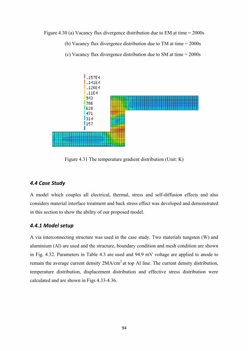
94
Figure 4.30 (a) Vacancy flux divergence distribution due to EM at time = 2000s
(b) Vacancy flux divergence distribution due to TM at time = 2000s
(c) Vacancy flux divergence distribution due to SM at time = 2000s
Figure 4.31 The temperature gradient distribution (Unit: K)
4.4 Case Study
A model which couples all electrical, thermal, stress and self-diffusion effects and also
considers material interface treatment and back stress effect was developed and demonstrated
in this section to show the ability of our proposed model.
4.4.1 Model setup
A via interconnecting structure was used in the case study. Two materials tungsten (W) and
aluminium (Al) are used and the structure, boundary condition and mesh condition are shown
in Fig. 4.32. Parameters in Table 4.3 are used and 94.9 mV voltage are applied to anode to
remain the average current density 2MA/cm2 at top Al line. The current density distribution,
temperature distribution, displacement distribution and effective stress distribution were
calculated and are shown in Figs 4.33-4.36.
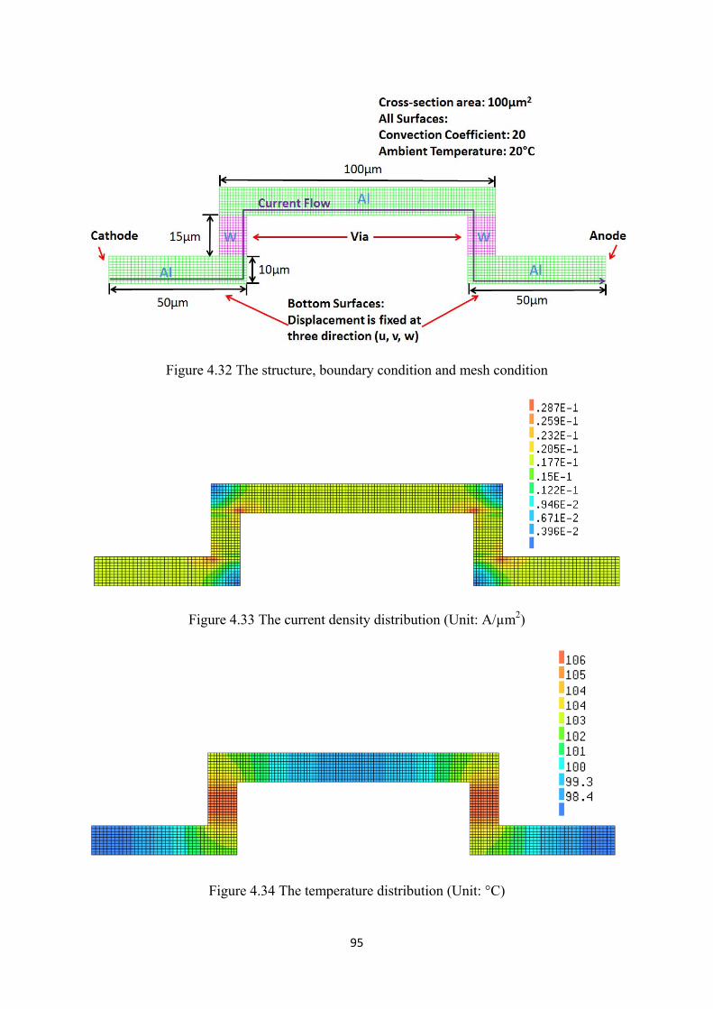
95
Figure 4.32 The structure, boundary condition and mesh condition
Figure 4.33 The current density distribution (Unit: A/µm2)
Figure 4.34 The temperature distribution (Unit: °C)

96
Figure 4.35 The displacement distribution (Unit: µm) and deformation (Deformation scaling
factor: 75)
Figure 4.36 The effective stress distribution (Unit: Pa) and deformation (Deformation scaling
factor: 75)
The maximum current density has been recorded at the top corners as Fig. 4.33 and tungsten
has been recorded with the maximum temperature due to tungsten’s higher electrical

97
resistance. The temperature gradient distribution and hydrostatic stress distribution were then
calculated as Figs. 4.37 and 4.38. As expected, the maximum current density, the highest
temperature gradient and the highest hydrostatic stress are recorded at the material interface
corners.
Figure 4.37 The temperature gradient distribution (Unit: °C/µm)
Figure 4.38 The hydrostatic stress gradient distribution (Unit: Pa/µm)
4.4.2 EM Analysis and Void Evolution
The EM analysis starts from the simplest scenario, electrical effect and self-diffusion effect
were coupled to be validated first. The equation (4.16) was used as governing equation and

98
the normalized vacancy distribution at time 10s, 100s, 800s are shown in Figs. 4.39 and 4.40.
Since the length of bottom Al strip is 100µm long which is same as the R.L. de Orio’s model
and parameters and current density used are also same as the R.L. de Orio’s analytic solution,
the vacancy distribution at the cathode and anode of the bottom Al strip (Fig. 4.39) is in
accordance with the data in Fig. 4.4.
Figure 4.39 The normalized vacancy distribution at time 10s.

99
Figure 4.40 The normalized vacancy distribution of bottom Al strip at time (a) 10s (b) 100s
and (c) 800s.
From Figure 4.39, it can be seen that the vacancy condensation appears at the cathode and
cathode side corner. Since the current density crowds at the cathode-side corner, the highest
drift velocity of the electrical effect at this corner has been recorded as the maximum value.
The normalized vacancy concentration value 1.2 is assumed as the critical value to form void
and relevant elements becomes “dead elements” when void formed, voids growth and
vacancy concentration distribution change then can be calculated as shown in Fig. 4.41 and
4.42 and the voids growth history highly agree with the data in Fig. 4.22.

100
Figure 4.41 Voids growth at time (a) 17s (b) 33s (c) 42s (d) 48s (e) 51s (Red elements
represent the “dead elements”)

101
Figure 4.42 The recorded maximum vacancy concentration evolution at time (a) 17s (b) 33s
(c) 42s (d) 48s (e) 51s
4.4.3 Analysis of Thermal Effects
Due to the low electrical conductivity of tungsten, the temperature within tungsten is higher
than the temperature within Al (Fig. 4.34). The temperature gradient distribution from Fig.
4.37 shows the peak temperature gradient value was recorded at both up corners because
there are with the highest current density which generates the most Joule heat. With the
paratmeters in Table 4.3, the drift velocity of thermal effect only can be calculated (Fig. 4.43)
and its relevant vacancy concentration change can be recorded as shown in Fig. 4.44. It is
worth noting that because the atoms always move from a high temperature area to a low
temperature area, the vacancy flux in this structure flows from top Al line into tungsten vias
at both corners as Fig.4.43 shows. The maximum temperature gradient was recorded at two
up corners as 0.73 °C/µm as Fig. 4.37 and therefore at both up corners the maximum drift
velocity of thermal effect was recorded as 0.0244 µm/s. That is to say, at the cathode side
corner, the thermal effect reduces the speed of vacancy accumulation and, at the anode side
corner, the thermal effect increase the speed of atoms accumulation.

102
Figure 4.43 The drift velocity distribution in value and in vector of thermal effect only (the length of vector represents intensity of drift velocity). (a) drift velocity distribution (Unit:
µm/s), (b) vacancy flux vector and (c) atomic flux vector.
Fig. 4.44 shows the vacancy distribution comparison between coupled self-diffusion and
electrical effects and coupled self-diffusion, electrical, and thermal effects at the time 10
seconds, we can see the vacancy concentration accumulation at cathode corner of thermal
coupled model is actually slower than that of non-thermal coupled model while the vacancy
concentration accumulation at anode corner of thermal coupled model is also slower than that
of non-thermal coupled model that means more atoms was pushed from tungsten side to Al
side.
We also used vacancy concentration value 1.2 as the critical value to simulate the voids
growth, the voids shape is same as shown in Fig. 4.41 but the time of voids formation is
much slower.

103
Figure 4.44 The normalized vacancy concentration distribution driven by (a) coupled self-diffusion and electrical effects and (b) coupled self-diffusion, electrical effect and thermal
effects at time 10s.
4.4.3 Analysis of Stress Effects
Since the thermal stress is partially dependent on the thermal effect, the thermal stress effect
shows a similar pattern as the thermal effect. As Fig. 4.38 shows, the maximum hydrostatic
stress gradient due to thermal expansion was recorded as 68.9 MPa/µm at the bottom Al lines
and 50.8 MPa/µm at up corners. Since the CTE of Al is much higher than CTE of tungsten,
the thermal expansion within the Al lines is greater than tungsten as shown in Figs. 4.35 and
4.36. Therefore, atoms were pushed from Al lines to tungsten vias and leave vacancies in Al
lines.

104
The maximum drift velocity of thermal stress effect was recorded as 0.294 µm/s at bottom Al
lines and 0.224 µm/s at up corners as shown in Fig. 4.45. It is interesting that the direction of
drift velocity of thermal stress effect at up corners shows separate phase, the direction of
outside elements’ drift velocity is from Al to tungsten and inside elements’ drift velocity is
from tungsten to Al. It can be explained by the compressive stress generated at both ends of
up Al lines while the tensile stress is generated at the up inside corners due to the thermal
expansion of top Al line as shown in Fig. 4.35.
Figure 4.45 The drift velocity distribution in value and in vector of thermal stress effect only (the length of vector represents intensity of drift velocity). (a) drift velocity distribution (Unit:
µm/s), (b) vacancy flux vector and (c) atomic flux vector.
Although the maximum drift velocity of the thermal stress effect at up corners is about ten
times greater than the thermal effect only, the opposite drift velocity of outside elements
offsets most of effective vacancy accumulating. The Fig. 4.46 shows the vacancy distribution
comparision between coupled self-diffusion and electrical effects and coupled self-diffusion,
electrical, and thermal stress effects at the time 10 seonds, the vacancy accumulation with

105
coupled thermal stress effect is just a little bit quicker and if we coupled thermal effect
together the thermal effect totally dominates the thermal stress effect.
The voids growth analysis also shows the same pattern as Fig. 4.41 by using normalized
vacancy concentration 1.2 as critical value.
Figure 4.46 the normalized vacancy concentration distribution driven by (a) coupled self-diffusion and electrical effects and (b) coupled self-diffusion, electrical effect and thermal
stress effects at time 10s.
The back stress effect was also coupled to the model and the vacancy accumulation at the
cathode corner was further retarded. Through comparison, we find that the contribution to the
void formation from high to low is electrical effect greater than thermal effect greater than

106
back stress effect greater than thermal stress effect for this via interconnecting structure.
However, the intensity of individual effects may perform very differnet in another specific
structure.
Figure 4.47 the normalized vacancy concentration distribution driven by (a) coupled self-diffusion and electrical effects and (b) coupled self-diffusion, electrical effect, thermal effect,
thermal stress effects and back stress effect at time 10s.
4.5 Conclusion
In this chapter, a new multi-physics simulation method has been proposed and implemented
in PHYSICA. This EM simulation method couples the thermal, stress (both external stress
and back stress), self-diffusion effects and void growth. It is the first model with the ability
to simulate the back stress effect to our best knowledge. We used an analytical solution
(electrical only effect) as the standard to compare the results of our model. We can conclude

107
that every individual part works well but the model is sensitive to the material properties such
as the activation energy. A via interconnecting structure is modelled to demonstrate the
numerical methods we used and the results highly consistent with realistic cases.
An atomic/vacancy divergence method has also been implemented on PHYSICA. This
method avoids the complexity of detailed EM analysis methods and can be used to analyse
the intensity of individual factors that contribute to EM damage. This method is very useful
for EM-aware microelectronics designer and can be used to estimate the MTTF of conductors
that are susceptible to EM failures.

108
CHAPTER 5: EM AWARE DESIGN
5.1 Introduction
The concern for potential failures caused by EM in microelectronics manufacture can be
addressed by a variety of design measures such as choosing conductor materials those are less
susceptible to damages caused by EM. EM-aware designs are those designs that have built-in
measures that mitigate the risk of EM failure. As EM is becoming a more and more important
issue, future EM-aware electronics designs need new tools and techniques. In this chapter, the
use of mathematical modeling method to analyze an interconnect design is presented. This
design reduces maximum current density in solder interconnects and therefore reduces the
risk of EM failure.
5.2 Design Factors
To talk about minimizing the damage of EM, we need to consider the factors which cause the
EM or may intensify the EM intensity. In this section, we will introduce these factors and
some possible optimizing ideas to mitigate the EM damage. Some ideas are also
demonstrated by our modelling analysis.
5.2.1 Material Selection
For a long time, Al-based metallization has been widely used in IC packaging because Al has
low resistivity, excellent adhesion to dielectrics can be easily deposited and can be dry etched.
However, R. Otten et al. [191] [192] [193] found that Al-Cu alloys can significantly improve
the EM resistance because of AlCu alloy’s higher activation energy as listed in Table 5.1.
Similarly, Lee, Hu, and Tu [194] found that adding Sn to Cu-metallization material can also
significantly increase activation energy and reduce EM drift velocity [194]. A material’s
susceptibility to EM damage can be described by drift velocity. If self-diffusion is ignored
and only electron-atom momentum transfer mechanism is considered, the drift velocity can
be described by Eq. (2.35a). If the parameters in Table 5.2 are used, the drift velocity value is
about 2.84 x10⁻¹⁵ m/s. If the activation energy Ea is reduced from 0.9eV to 0.7eV while other

109
parameters remain the same, the drift velocity increases to 5.07x10⁻¹⁵ m/s. Table 5.3 shows
how this improves the material’s resistance to EM.
Blech Product (A/cm)
Effective Charge
Number, Z*
Activation Energy Ea (eV) (373K - 473K)
Al 244 18 0.6 98Al2Cu 833 5 0.79
Table 5.1 EM resistance comparison between pure Al and AlCu. The higher Blech product value of AlCu alloy means it has higher EM resistance than pure Al.
+
Parameters Value T (Temperature) 310K
D0 (Pre-exponential Factor) 5.2 x 10⁻⁶ m2/s Ea (Activation Energy) 0.9eV Z* (Effective Charge) -5 Je (Current Density) 7.0 x10⁴ A/cm2
(Resistivity) 2.3 x 10⁻⁷ Ω*m Table 5.2 Parameters
Ea (eV) 0.9 0.7 v (m/s) 2.84 x 10⁻¹⁵ 5.07 x 10⁻¹²
Time for 1µm drift 11.2 years 54.8 hours Table 5.3 The drift velocity comparison for different activation energy Ea.
Local temperature of conductor appears in the exponent of Eq. (2.10) and this means that
temperature strongly impacts the lifetime of conductors. If conductors are kept at a low
temperature, EM will be greatly reduced because there is little atomic mobility of diffusion,
even though there is a driving force from electric current. Based on this point, selecting
materials with greater electrical and thermal conductivity are very helpful to reduce risks of
EM [195] [196].
5.2.2 Back Stress and Critical Length
The size of interconnect components may affect the intensity of EM. The regular interconnect
structure shown in Fig. 5.1 has many short segments. EM in such short segments tends to
induce back stress which retards atomic movement. The back stress is due to mechanical

stress b
for, the
section
short A
When s
thresho
length Llength, L < Lbecome
atomic
choosin
damage
Figu
As Hu e
cap laye
(higher
stress an
build up wh
atomic flow
2.2.1, the b
Al strips patt
strong curre
ld product L can be
, the con
es immortal
flow that is
ng conducto
e.
ure 5.1 SEMsurface. Th
et al. [198]
ers on top o
stiffness) b
nd therefore
hich causes
w towards t
back stress
terned on a
ents passed ( ∙ )
e defined (E
nductor wil
l. This happ
s driven by
or length in
M image of the width of
observed in
of the coppe
because suc
e enhance t
a reverse m
the anode un
was firstly
base line of
the Al stri
(Eq. 2.15)
Eq. 2.14). I
ll not suffe
pens becaus
electric cur
situations w
two-level Af the line an
n their work
er metal and
ch surface c
the reverse
110
migration pr
nder the inf
y recognized
f TiN as dep
ips, they fou
and if the
f the condu
er from EM
se the back
rrents. The c
where curren
Al (Cu) internd the spacin
k, Blech len
d by using d
coating can
migration.
rocess that
fluence of e
d by by Ble
picted in Fi
und a proce
e current de
uctor length
M damage
stress fully
critical leng
nt density c
rconnect lineng between
ngth can be
dielectrics w
n form a rig
reduces, or
lectron win
ech and Her
g. 2.5 [54]
ess and tech
ensity is a
h L is short
and the c
compensat
gth provides
cannot be re
es with W-pthem is 0.5
increased b
with a higher
gid wall wh
r even comp
nd. As ment
rring using
[55] [56] [5
chnology de
constant a
ter than the
conductor th
tes for the e
s us a good
educed to av
plug vias on5 µm [197].
by depositin
er Young’s m
hich increas
pensates
tioned in
a set of
57] [58].
ependent
a critical
e critical
i.e.
herefore
effective
rule for
void EM
n a Si
ng (stiff)
modulus
ses back

111
5.2.3 Bamboo Structure and Slotted Wires
Generally speaking, the reduction of wire width will generate higher current density and
temperature and both of them harm the reliability of wire. However, if the wire width is
reduced to below the average grain size of the wire material, the EM resistance of wire
increases, despite an increase in the current density. This apparent contradiction is caused by
the microstructure and diffusion path of metals. When grain size in a conductor is greater
than the width of the conductor, atoms diffuse quickly along those grain boundaries that are
more or less aligned with the current flow direction. In wires where line width is smaller than
grain size, the grain boundaries are more or less perpendicular forming a so called “bamboo
like structure” (Fig. 5.2). As the main material transport pathway, grain boundary diffusion in
this bamboo structure is therefore perpendicular to the current flow (also atomic flow), and
this results in slower material transport along the direction of electron flow.
Figure 5.2 Reduced wire width – less than the average grain size – improves wire reliability
with regard to EM.
Based on this material property, wire widths can be deliberately kept narrow enough to
maintain a bamboo structure to suppress EM. The wire material can be annealed selectively

112
during IC manufacturing processing in order to support the formation of bamboo structure
[190].
However, the maximum possible wire width for a bamboo structure is often still too narrow
for signal lines carrying large-magnitude currents in analog circuits or for power supply lines
[199]. In these circumstances, slotted wires which have rectangular holes have been
introduced. Hence, the widths of the individual metal structures in between the slots can have
a bamboo structure, while the total width of all the metal structures combined meets power
requirements.
5.2.4 Reservoir Effect
The theory of the so called “reservoir effect” is quite simple but it can significantly improve
the lifetime of via interconnecting part [200]. Under some circumstances we can increase the
metal-via layer overlap to enlarge the amount of interconnect material. The technique is
called “overhang” and its effect on time-to-failure is shown schematically in Fig. 5.3. The
overhang can be considered as a source of atoms and can continuously supply atoms to the
conducting part when directional atomic movement happens. It is worthy to note that
overhang should be put at the cathode side and it does not decrease EM but it prolongs the
lifetime of connecting part. The negative effect of overhang is that it increases the length of
the conductor which reduces possible back stress build-up. Therefore, the design of hangover
needs to be considered in conjunction with the effect of conductor length.

113
Figure 5.3 Reservoir effect: (a) a regular via structure without overhang (b) a via structure
with overhang.
5.3 Conductor Design and Optimization
To reduce EM risk, the first thing to do is to avoid excessive current crowding so that the
maximum current density can be kept low. This can be done through careful design of
conductor lay out as demonstrated later in this section. Because the temperature in conductors
is determined by the ambient temperature as well as the heat that’s generated by electricity
(Joule heat), the temperature and current density factors are closely linked, and by reducing
maximum current density, hotspot and temperature gradient can also be controlled. In
sections 5.3 and 5.4, the work is focused on designs that minimize the current crowding. The
design optimization process can be achieved by using numerical analysis method to predict
current density for conductors of a range of geometric shapes.
5.3.1 Interconnects Design and Optimization
According to the Blech product in Eq. (2.15), a relationship between the minimum cross
section area of a conductor and the maximum current density can be established. Based on
these relations, the minimum width and minimum height ℎ of the conductor can be
obtained (Fig. (5.4)).

114
Figure 5.4 schematic cross section area of conductor
= ∙ ( ), ∙ _ (5.1)
ℎ = ∙ ( ), ∙ ℎ _ (5.2)
where is the peak current under working condition, ( ) is the safe factor which can be
defined as the ratio of between the electrical conductivity at reference temperature and
the electrical conductivity at working temperature (T), , is the maximum current
density the conductor can sustain to meet the maximum Blech product and w and h are the
width and height needed for structure design respectively. According to the revised Black’s
model (Eq. (2.11)), an increase in temperature reduces the maximum permissible current
density in order to maintain a specific life time of the conductor. Hence, a temperature
scaling factor f(T) can be derived from Eq. (2.11) which takes this current-density reduction
into account (Eq. (5.3)). If the wire width/height variation and etch loss wetch/hetch during
manufacturing stage are also taken into account, the minimum width (Eq. (5.1)) and
minimum height ℎ (Eq. (5.2)) can be revised to yield Eqs. (5.4) and (5.5) respectively.
( ) = exp (− 1 − ) (5.3)
= ( ∙ ( ), ∙ + ) ∙ ( ) _ + ∙ ( ) (5.4)

115
ℎ = ( ∙ ( ), ∙ + ℎ ) ∙ ( ) ℎ _ + ℎ ∙ ( ) (5.5)
Based on similar theory, designers can improve the via array arrangement by replacing a
single via with a via array or adjusting the number of vias in a via array. The temperature
dependent number of vias Nvia(T) that are required within a via array can be obtained by: ( ) = _ ,( )∙ ( ) ∙ (5.6)
where is the equivalent current that the whole via array must sustain, _ ,( ) is
the maximum permissible current value of a single via at the reference temperature, g is the
inhomogeneity current flow factor which is characterized as the highest current density
through single via/lowest current density through single via within the via array. The
minimization of inhomogeneity of current flow will be covered in the next section.
5.3.2 Corner Angle and Via Arrangement
Current crowding is a major issue for microelectronics designers. Wire corners, vias, and
solder bumps are typical structures where serious current crowding may occur. Current
crowding generates high current density, high temperature, and great temperature gradients,
which contribute to EM and TM. Thus, homogenization of current density distribution is the
key to reduce atomic migration. In the following, a few cases will be shown and techniques
of current crowding reduction will be discussed.
To illustrate how current crowding in conductors with corners can be reduced, the electric
current density distributions in three cornered copper conductors have been modelled. The
electrical resistivity of copper is assumed to be 1.6x10⁻⁸ Ω*m, the total current load is 2A,
and the cross-section’s dimensions are 200µm x 200µm for all the models. The results are
shown in Fig. 5.5. The maximum current density for the three models are 1.79 x 10⁴ A/cm2
(90° angle), 9.86 x 10³ A/cm2 (45° angle), and 6.95 x 10³ A/cm2 (round) respectively. This
case shows how important the conductor geometry to current distribution.

116
Figure 5.5 Current density distributions of corners with different angles. (Units: A/m2)
A similar example is about the distribution of current density in tungsten vias. These vias are
widely used in semiconductor manufacturing are part of IC circuit. Due to the limited
ampacity of each individual via, an array of tungsten vias are usually used. As shown in
Fig. 5.6, by redistributing the vias, maximum current density can be reduced significantly.
These two examples show that if possible, conductors have round corners can greatly
minimize the EM intensity.
Figure 5.6 current crowding can be reduced by rearranging tungsten via array.

117
5.3.3 Mitigate Current Crowding in Solder Joint
Solder alloy has lower current carrying capacity than Al/Cu because it’s more susceptible to
EM due to its low melting point and the lattice diffusion being dominant over grain diffusion
and surface diffusion. Higher atom mobility is expected when lattice diffusion is strong [10].
In designing a solder interconnect, solder joint cross section must be large enough so that EM
does not cause significant damage. In the situation where solder joint dimensions are
restricted, there is the risk that current crowding cause local current density to rise above the
threshold for EM even if the average current density is below the threshold.
A solder joint model is shown in Fig. 5.7 and in Fig. 5.8 current crowding can be seen to
occur at solder joint corners of this model (cycled area). By reducing current density at these
current crowding locations, the reliability of solder joints can be improved. Under pure
electric loading, the lifetime of solder joint is inversely proportion to the square of current
density based on the Black’s model Eq. (2.10).
Figure 5.7 the structure of a typical solder joint
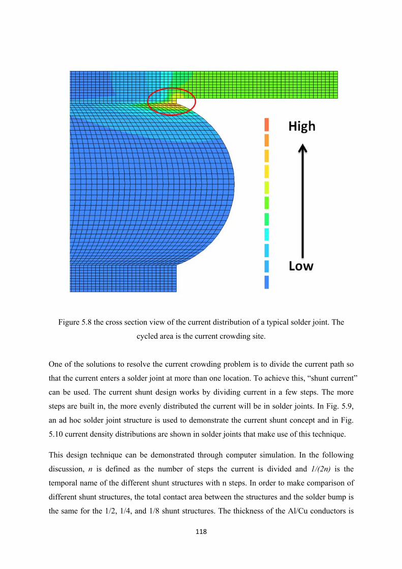
118
Figure 5.8 the cross section view of the current distribution of a typical solder joint. The
cycled area is the current crowding site.
One of the solutions to resolve the current crowding problem is to divide the current path so
that the current enters a solder joint at more than one location. To achieve this, “shunt current”
can be used. The current shunt design works by dividing current in a few steps. The more
steps are built in, the more evenly distributed the current will be in solder joints. In Fig. 5.9,
an ad hoc solder joint structure is used to demonstrate the current shunt concept and in Fig.
5.10 current density distributions are shown in solder joints that make use of this technique.
This design technique can be demonstrated through computer simulation. In the following
discussion, n is defined as the number of steps the current is divided and 1/(2n) is the
temporal name of the different shunt structures with n steps. In order to make comparison of
different shunt structures, the total contact area between the structures and the solder bump is
the same for the 1/2, 1/4, and 1/8 shunt structures. The thickness of the Al/Cu conductors is

119
kept constant and therefore the width of contacting area at each level, Wn, can be calculated
using Eq. (5.7) from WAl which is the cross section area of the thickest conductor in the 1/2,
1/4 and 1/8 structures. The solder bump in this study has a diameter of 500 µm.
= (5.7)
Figure 5.9 (a) Basic structure without current division, (b) 1/2 shunt structure, (c) 1/4 shunt
structure and (d) 1/8 shunt structure.

120
Figure 5.10 top view of the current density distribution in solder joints (Unit: A/m2).
The properties of copper and aluminium are listed in Table 5.2 and a current of 1.8 A is
applied to the solder joints. The current density distributions the solder interconnects are
shown in Fig. 5.10. The maximum current density of the solder bumps is 8.27 x 10² A/cm2,
3.54 x 10² A/cm2, 3.5 x 10² A/cm2, and 3.2 x 10² A/cm2 respectively. This means that the
maximum current density can be reduced by 57.3% if the 1/8 structure is adopted in the
design, and this may prolong the solder joint lifetime time by about five times according to
the Black’s model. The reduction in the maximum current density is the results of more even
current density distribution as shown in Fig. 5.11. These results show that the current shunt
design has great potential in reducing current crowding and enhancing solder joint EM
resistance.

121
Figure 5.11 the top view of the current density (A/m2) distributions in solder bump
5.4 EM-Aware Design Rule and Standard Processing
Modern IC design and manufacturing relies heavily on Electronic design automation (EDA)
[201] techniques that are implemented using various software tools. The use of EDA can
shorten the product development cycle and improve product performance. A typical IC
design using EDA techniques is shown in Fig. 5.12 [202] . However, EM as a serious threat
in future IC design has not been seriously considered and treated in IC EDA.

122
Figure 5.12 The flow chart of modern IC design [202].
In this section, an EM-aware IC design process will be introduced and suggested to be added
in the modern EDA process. Generally speaking, any designing effort to resist EM should be
made at the physical design stage of EDA because all circuit components and interconnecting
structures are placed and mapped at physical design stage as Fig. 5.12 shows. The proposed
EM-aware designing process is added between the step “placement” which means software
assigns exact locations for various circuit components within the chip’s core area and the step
“signal routing” which means software add wires or interconnecting structures needed to
properly connect the placed components while obeying all IC designing rules as Fig. 5.13.

123
Figure 5.13 The flow chart of proposed EM-aware design process.
As Fig. 5.13 shows, the proposed EM-aware design process includes three main modules:
the current-driven routing module, the EM-robust verification module and the EM-robust
optimization module. The current-driven routing applying EM-aware strategies to route the
power supply conductors of IC circuits. The EM-robust verification module is to determine if
the intensity of EM exceeds the maximum EM tolerance of the conductors under predefined
working environmental conditions (i.e. the working temperature) of the chip. EM-robust
optimization module is a process of combined EM optimization implementation that
optimizes the relevant designing structures which have been identified as EM “violating areas”
in the EM-robust verification process. In the following, the detailed working process and
mechanism of three modules will be introduced individually.
5.4.1 Current-Driven Routing Module
An schematic diagram of the suggested current-driven routing module is shown in Fig. 5.14.
The routing module is divided into three individual steps: (1) topology planning and pin
connection check. (2) calculating the required wire width and vias size and (3) the final
routing using the calculated wire and vias dimensions.

124
Figure 5.14 The schematic diagram of the suggested current-driven routing stage.
It is worth noting that a reference working temperature need to be estimated to calculate the
widths/heights of wires and the number of vias of via arrays (Eqs. (5.4)-(5.6)) before running
the current-driven routing module. In addition, the maximum current densities that are
allowed also need to be calculated in advance according to the planned wire length and Blech
products (Eq. (2.15)).
At the beginning of the current-driven routing module, the net topology need to be
determined by calculating an optimized routing tree based on Kirchhoff’s current law [203].
For example, the Fig. 5.15 shows two cases of different net topology with the same four
terminals but the intensity and direction of current flow are different for two cases as shown
in Fig. 5.15.

125
Figure 5.15 The different current flow patterns within different net topologies [204].
After the net topology is defined, the obtained net segment currents will be used to calculate
the minimum wire width/height and via arrays by using Eqs. (5.4)-(5.6). Since maximum
tolerant current densities have already been taken into account during this planning phase, the
detailed final routing with calculated layout size of wires and vias could then be calculated
and sent to next module.
5.4.2 EM-robust Verification Module
The task of EM-robust verification module is designed to validate that the intensity of EM
within the designed structure will remain at an acceptable level and the life time of the
designing structure can meet the designed requirements under predefined working
environment.
With the well planned wires and vias routing by current-driven routing module, various
analysis methods (i.e. finite element method) can be used to find out the most EM-
endangered areas of the interconnecting structures. The suggested analysis of EM-robust
verification should include the current density verification, thermal and TM analysis,
mechanical stress and SM analysis and voids growth and MTTF simulation as shown in Fig.
5.16. In the current density verification stage the current density distribution is calculated
and the life time of relevant structures is obtained. If the life time of the structures cannot

126
meet the requirement, those structures will be marked as “violating” and the structure will be
optimized by EM-robust optimization module. Similar mechanisms are applied to thermal
and TM analysis, stress and SM analysis and MTTF simulation. The life time of structures
that are being designed will be calculated and evaluated using TM model and SM model
respectively, the areas with high temperature gradient and hydrostatic stress gradient will be
marked as “violating” structures and will be improved by the EM-robust optimization module.
Figure 5.16 The schematic diagram of the suggested EM-Robust verification module.
It is worth noting that the type of EM analysis can be chosen case by case to meet the time
requirements. For some simple cases (i.e. the designing IC is supposed to work at a low
temperature environment), only current density verification analysis could be enough as the
TM will not be a problem. Also the atomic/vacancy divergence model can be used as an
analysis method in this module.

127
5.4.3 EM-robust Optimization Module
The major goals of the EM-robust optimization module are to adjust layout segments of
“violating” structures and homogenize the current density, temperature and hydrostatic stress
distribution. The module can be divided into three parts as shown in Fig. 5.17. In this module,
designing factors introduced in section 5.2 and 5.3 can be used to improve the EM resistance
of “violating” interconnecting structures. During the wires & via-array sizing, the size of
wires and number of via-array will be optimized without affecting neighbouring
interconnecting structures. If the space of “violating” areas is limited, the supporting
structures will be calculated and evaluated to add into the exist structures to mitigate the EM.
The final optimized layout will be generated by the layout decompaction and be sent back to
current-driven routing module to evaluate the EM robust of designing structures.
Figure 5.17 The schematic diagram of the suggested EM-Robust optimization module
An example of EM-roubust optimized structure is depicted in Fig. 5.18. The “violating” areas
are marked by EM-robust verification module and after calculating by EM-robust
optimization module, the width of wires is increased without affecting neighbouring
interconnecting structures and two polygons supporting structures are added to rectangle

128
corners to homogenize the current density. The final layout of structure then will be sent back
to the current-driven routing module to recalculate.
Figure 5.18 (a) net with “violating” area (pink area representing “violating” area is with high current density) compared to (b) optimization net (green areas are optimized by wire & via-
array sizing part, red areas are optimized by the addition of a support structure part).
In addition, conductor design techniques such as slotted wires, “overhang” structure and
“current shunt” structures can also be coded to this module and be used to improve the EM
resistance. With the increased understanding of the EM, we believe that more and more
optimizing methods will be proposed to mitigate EM threat in near future.
5.5 Conclusion
In this chapter, the factors that affect EM have been discussed. EM risk mitigation methods
that are based on the analysis of these factors have been discussed. Since one of the key
factors in the EM process is the current density, a new solder joint interconnect structure has
been proposed and its effect in reducing the maximum current density and EM intensity has
been demonstrated and verified using Finite Element method. A suggested EM-aware
designing rule has been proposed and it can be coded into EDA software to avoid EM failures
of microelectronics devices. The mechanism and standard process of the suggested EM-
aware designing rule have been introduced and discussed.
129
CHAPTER 6: CONCLUSION AND FUTURE WORK
6.1 Conclusion
EM is phenomenon that poses a great threat to electronics devices reliability. As
semiconductor product becomes ever more miniaturised and powerful, it will become a bottle
neck in electronics design because of the possible EM damage caused by high current density.
This research work has used numerical simulation to help understand EM and to help
electronics design engineers to create designs that are not susceptible to EM damage. The
work has been focused on the numerical modelling techniques of EM, the EM process in thin
solder films, and an interconnect design that reduces current crowding.
In this work, we reviewed and discussed various EM models from simple ones to
complicated ones in chronological order. A new multi-physics model was also proposed and
developed which includes all effects of EM as far as we know. That is finally to be able to
predict the atomic/vacancy distribution, voids growth and therefore to be able to predict the
MTTF of microelectronic structure. This new numerical model could be very useful to
understand and study mass migration for researchers and to provide a tool for
microelectronics designing in the issue of EM.
A very thin (600nm) Pb-free solder film has been manufactured for investigating the pure
electrical effect of EM behaviour in the solder. The experiment was designed in such a way
that temperature gradient and stress can be ignored. The film is very thin and therefore the
out of plane stress is negligible. By using ANSYS and PHYSICA, this experiment design
was proved a success also with regards to the temperature gradient effect on EM. A
transparent glass substrate was used the solder film and in this novel way, voids can be
observed on both sides and the voids evolution process had been checked and recorded by
using SEM, AFM and electrical resistance measurement regularly. Under a high current
density stressing 6×10⁴ A/cm2, voids appear at around 983 hours and the experiment was
stopped when the electrical resistance increased by 10% to avoid the specimen being burnt
and evidence of EM destroyed. The first voids appeared at the highest current density area
and new voids basically appeared at the new maximum current density area. Some voids
formed at the middle of the specimen and it can be explained by the existence of defects. A
full current density analysis was used to explain the void growth history. It was found that the
appearance of the initial voids quite match what is expected but the voids evolution at a later

130
stage does not match simulation result. Other methods have been tried to address issue. For
example, instead of using a critical current density as the void formation criteria, critical
current density gradient has been used but no conclusive results have been obtained. Further
work is needed.
A new multi-physics simulation method has been proposed implemented in PHYSICA. This
EM simulation method couples the thermal, stress (both external stress and back stress), self-
diffusion effects and voids growth. It is the first model with the ability to simulate the back
stress effect to our best knowledge. We used an analytical solution (electrical only effect) as
the standard to compare the results of our model. We can conclude the every individual part
works well but the model is sensitive to the material properties such as the activation energy.
A via interconnecting structure is modelled to demonstrate the numerical methods we used
and the results highly consistent with realistic cases.
An atomic/vacancy divergence method has also been used in this work. This method avoids
the complexity of detailed EM analysis methods and can be used to analyse the intensity of
individual factors that contribute to EM damage. This method is very useful for EM-aware
microelectronics designer and can be used to estimate the MTTF of conductors that are
susceptible to EM failures.
The factors that affect EM have been reviewed in the context of EM-aware design. EM risk
mitigation methods and design rules that are based on the analysis of these factors have been
discussed. Since one of the key factor in EM process is the current density, a new solder joint
interconnect structure has been proposed and its effect in reducing the maximum current
density and EM intensity has been demonstrated and verified using Finite Element method.
6.2 Future Work
Further work is required to study and characterize the EM behaviour and especially the EM
behaviour of Pb-free soldering materials which has replaced the traditional SnPb solder
material in most industrial sectors. One of the most important areas of work is to investigate
the methodology of parameters measurement because an accurate EM modelling is extremely
sensitive to the parameters used.
The numerical methods that have been developed in this work can provide lots of information
for electronics designers and manufacturers for EM resistance designs, but it is a

131
phenomenon that is still not well understood. The current simulation method cannot always
predict the correct void initiation and evolution yet. The mathematical model needs to be
developed further in order to capture more physical processes in current carrying conductors.
For example, at the moment, microstructure changes in conductors are not factored in.
Even in its current form, the numerical method can be improved further. For example, in the
voids evolution simulation, by using an iterative method the properties of a conductor can
change gradually as vacancy concentration increases.

132
REFERENCES
[1] A. a. p. section, "the International Technology Roadmap for Semiconductor (ITRS)," 2007.
[2] A. a. p. section, "2009 International technology roadmap for semiconductors," Semiconductor Industry Association, 2009.
[3] G. E. Moore, "Excerpts from A Conversation with Gordon Moore: Moore’s Law," Intel Corporation, 2005.
[4] G. E. Moore, "Moore's Law" Predicts the Future of Integrated Circuits," Computer History Museum, 1965.
[5] G. E. Moore., "Cramming more components onto integrated circuits," Electronics Magazine, vol. 38, no. 8, p. 4, 1965.
[6] D.J. Alcoe, T.E.Kindl, J.S.Kresge, J.P. Libous, C.L.Tytran-Palomaki, R.J.Stutzman, "A high Performance, Low Stress, Laminate Ball Grid Array Flip Chip Carrier," in Semiconductor Packaging Technologies Symposium, SEMICON West, 1999.
[7] R. Fillion, "Advanced Packaging Technology for Leading Edge Microelectronics and Flexible Electronics," GE Global Research, Ray Fillion, Advanced Packaging Technology for Leading Edge Microelectronics and Flexible Electronics, GE Global Research, http://people.ccmr.cornell.edu/~cober/mse542/page2/files/Fillion%20GE.pdf.. [Online]. Available: http://people.ccmr.cornell.edu/~cober/mse542/page2/files/Fillion%20GE.pdf. .
[8] I. Ames, F. M. d'Heurle abd R. Horstman, IBM J. Res. Dev., vol. 4, p. 461, 1970.
[9] I. section, "International technology roadmap for semiconductors," San Jose: Semiconductor Industry Association, 2003.
[10] K. Tu, Solder joint technology: materials, properties, and reliability, Springer Science, 2007.
[11] Hey, H.P.W. , Sinha A. K, Steenwyk S.D, Rana V.V.S., Yeh J. L, "Selective tungsten on aluminum for improved VLSI interconnects," in 1986 International Electron Devices Meeting, 1986.
[12] G. M., "C. R.," in AcadSci Paris, 53:727, 53:727, 1861.
[13] H. Ye, C. Basaran and D. C. Hopkins, "Thermomigration in Pb-Sn solder joints under Joule heating during electric current stressing, Applied Physics Letter," Applied Physics Letter, vol. 82, no. 7, pp. 1045-1047, 2003.
[14] Annie T. Huang, K. N. Tu, "Effect of the Combination of Electromigration and Thermomigration on Phase Migration and Partial Melting in Flip Chip Composite SnPb Solder Joints," J. of Appl. Phys., vol. 100, no. 033512, 2006.

133
[15] D. Yang, M.O. Alam, B.Y. Wu, Y. C. Chan, "Thermomigration in eutectic tin-lead flip chip solder joints," in 8th Electronics Packaging Technology Conference, pp. 565-569, Singapore, 2006.
[16] S. Brandenburg and S. Yeh, "Electromigration studies of flip chip bump solder joints," in the Surface Mount International Conference and Exhibition (SMI, San Jose, CA), 1998.
[17] Yuan Guangjie and Chen Leng, "Finite Element Simulation of Hydrostatic Stress in Copper Interconnects," Journal of Semiconductors, vol. 32, no. 5, 2011.
[18] L. T. Shi and K. N. Tu, "Finite-element Modelling of Stress Distribution and Migration in Interconnecting Studs of a Three Dimensional Multillevel Device Structure," Applied Physics Letter, vol. 65, no. 12, 1994.
[19] D.Ang, R.V.Ramanujan, "Hydrostatic stress and hydrostatic stress gradients in passivated copper interconnects," Materials Science and Engineering, pp. 157-165, 2006.
[20] F. Fantini, J. R. Lloyd, I. De Munari, and A. Scorzoni, Microelectron. Eng., vol. 40, 1998.
[21] M. Hauder, J. Gsto¨ttner, W. Hansch, and D. Schmitt-Landsiede, Appl. Phys. Lett., vol. 78, no. 838, 2001.
[22] M. Hauder, W. Hansch, J. Gsto¨ttner, and D. Schmitt-Landsiedel, Microelectron. Eng., vol. 60, no. 51, 2002.
[23] Alford TL, Adams D, Laursen T, Ullrich BM., "Encapsulation of Ag films on SiO2 by Ti reactions using Ag–Ti alloy/bilayer structures and an NH3 ambient.," Appl Phys Lett, vol. 68(23):3251–3, 1996.
[24] Manepalli R, Stepniak F, Bidstrup-Allen SA, Kohl P., "Silver metallization for advanced interconnects," IEEE Trans Adv Packag , no. 22(1), 1999.
[25] Hauder M, Gst€ottner J, Hansch W, Schmitt-Landsiedel D., "Scaling properties and electromigration resistance of sputtered Ag metallization lines.," Appl Phys Lett, vol. 78(6), 2001.
[26] Y. Wang and T. L. Alford, Appl. Phys. Lett., vol. 74, no. 52, 1999.
[27] L. Chen, Y. Zeng, P. Nyugen, and T. L. Alford, Mater. Chem. Phys., vol. 76, no. 224, 2002.
[28] T. L. Alford, L. Chen, and K. S. Gadre, Thin Solid Films , vol. 429, no. 248, 2003.
[29] D. G. Pierce and P. G. Brusius, Microelectron. Reliab. , vol. 37, no. 1053, 1997.
[30] E. Misra and T. L. Alford, Appl. Phys. Lett., vol. 172111, 2005.
[31] Shekhar Bhagat, N. David Theodore, Santhosh Chenna, and Terry Alford, "Effect of Copper Addition on Electromigration Behavior of Silver Metallization," Applied Physics Express, vol. 2,

134
2009.
[32] M. Hauder , W. Hansch, J. Gst€ottner, D. Schmitt-Landsiedel, "Ag metallization with high electromigration resistance for ULSI," Solid-State Electronics, vol. 47, pp. 1227-1231, 2003.
[33] M.O. Alam, B. Y. Wu, Y. C. Chan and K.N. Tu, "High electric current density-induced interfacial reactions in micro ball grid array (μBGA) solder joints," Acta Materialia, vol. 54, pp. 613-621., 2006.
[34] H. D .Blair, T. Y. Pan and J. M. Nicholson, "Intermetallic compounds growth on Ni, Au/Ni, and Pd/Ni substrates with Sn/Pb, Sn/Ag and Sn. Solders," in 48th Electronic Components & Technology Conference May 25-28, pp. 259-26, Seattle, Washington, USA, 1998.
[35] Boon-Khim Liew, Nathan W. Cheung, Chenming Hu, "Projecting Interconnect Electromigration Lifetime for Arbitrary Current Waveforms," IEEE Transactions on Electron Devices, vol. 37, no. 5, pp. 1343-1351, 1990.
[36] E. Castano, J. Maiz, P. Flinn, M. Madden, "In situ Observations of dc and ac electromigration in passivated Al lines," Appl. Phys. Lett., vol. 59, no. 1, pp. 129-131, 1991.
[37] K.-D. Lee, "Electromigration Recovery and Short Lead Effect under Bipolar- and Unipolar-Pulse Current," Vols. 978-1-4577-1680-5, no. Electromigration Recovery and Short Lead Effect under Bipolar- and Unipolar-Pulse Current, 2012.
[38] L. M. Ting, "AC Electromigration Characterisation and Modeling of Multilayered Interconnects," IEEE, Inter. Reliab. Physic Symp, pp. 311-316, 1994.
[39] J. Tao, "An Electromigration Failure Model for Interconnects Under Pulsed and Bidirectional Current Stressing," Electron Device Letters, vol. 41, no. 4, 1994.
[40] J. Tao, "Modelling Electromigration Lifetime Under Bidirectional Current Stress," Electron Device Letters, vol. 16, no. 11, 1995.
[41] P. Waltz, "Analyse et Modélisation de la Tenue àl’Electromigration des Interconnections en Régime Dynamique," Thèse de doctorat INSA Lyon, pp. 229-231, 1998.
[42] L. Doyen, X.Federspiel, D. Ney, "IMPROVED BIPOLAR ELECTROMIGRATION MODEL," in 44th Annual International Reliability Physics Symposium, San Jose, 2006.
[43] J. M. Towner, E. P. van de Ven, "Aluminum Electromigration Under Pulsed D.C. conditions," in Reliability Physics Symposium, 1983.
[44] L. Brooke, "Pulsed Current Electromigration Failure Model," in Reliability Physics Symposium, 1987.
[45] J. A. Maiz, "Characterization of electromigration under bidirectional (BC) and Pulsed

135
unidirectional (PDC) currents," in Reliability Physics Symposium, 1989.
[46] E. Petitprez, L. Doyen, D. Ney, "Temperature scaling of electromigration threshold product in Cu/low-k interconnects," in IRPS, 2009.
[47] K.-D. Lee, E. T. Ogawa, S. Yoon, X. Lu, P. S. Ho, "Electromigration reliability of dual-damascene Cu/porous methylsilsesquioxane low k interconnects," Applied Physics Letters, vol. 82, no. 13, p. 2032, 2003.
[48] P. C. Wang and R. G. Filippi, "Electromigration threshold in copper interconnects," Applied Physics Letters, vol. 78, no. 23, p. 3598, 2001.
[49] R.L. de Orio, H. Ceric, S. Selberherr, "Physically based models of electromigration: From Black’s equation to modern TCAD models," Microelecronics Reliability, pp. 775-789, 2010.
[50] J. R.Black, "Electromigration failure modes in aluminum metallization forsemiconductor devices," Proc IEEE Lett, vol. 57(9), no. 1578–94, 1969.
[51] H. B. Huntington and A. R. Grone, "Current-induced marker motion in gold wires," J. Phys. Chem. Solids, vol. 20, no. 76, 1961.
[52] Blair JC, Ghate PG, Haywood CT., "Concerning electromigration in thin films," Proc IEEE Lett, vol. 59, no. 1023–4, p. 59, 1971.
[53] Huntington, H.B and Grone,A.R., "J.Phys Chem. Solid," vol. 20, no. 76, 1961.
[54] B. I.A., "Electromigration in thin aluminum films on titanium nitride," J Appl Phys, vol. 47(4), no. 1203–8, 1976.
[55] Blech I. A. , Herring C. , "Stress generation by electromigration," Appl Phys Lett, vol. 29(3), no. 131–3, 1976.
[56] Blech I. A. , Tai KL., "Measurement of stress gradients generated by electromigration," Appl Phys Lett , vol. 30(8), no. 387–9, 1977.
[57] E. T. Ogawa, A. J. Bierwag, K.-D. Lee, H. Matsuhashi, P. R. Justinson, and et al., "Direct Observation of a Critical Length Effect in Dual-Damascene Cu/Oxide Interconnects," Appl. Phys. Lett., vol. 78, no. 18, pp. 2652-2645, 2001.
[58] D. Ney, X. Federspiel, V. Girault, O. Thomas, and P. Gergaud, "Stress-Induced Electromigration Backflow Effect in Copper Interconnects," Trans. Dev. Mater. Reliab., vol. 6, no. 2, pp. 175-180, 2006.
[59] L. Doyen, E. Petitprez, P. Waltz, X. Federspiel, L. Arnaud, and Y. Wouters, "Extensive Analysis of Resistance Evolution due to Electromigration Induced Degradation," J. Appl. Phys, vol. 104, p. 123521, 2008.

136
[60] A. S. Oates and M. H. Lin, "Void Nucleation and Growth Contributions to the Critical Current Density for Failure in Cu Vias," in Proc. Intl. Reliability Physics Symp., 2009.
[61] Tan, C. M., and A. Roy., " Investigation of the effect of temperature and stress gradients on accelerated EM test for Cu narrow interconnects," Thin Solid Films, vol. 504, pp. 288-293, 2006.
[62] Ye, H., C. Basaran, and D. Hopkins, "Thermomigration in Pb-Sn solder joints under joint heating during electric current stressing," Applied Physics Letters, vol. 82, pp. 1045-1047, 2003.
[63] J. J. Clement and C. V. Tompson, "Modelling electromigration-induced stress evolution in confined metal lines," J. Appl. Phys., vol. 78, no. 2, pp. 900-904, 1995.
[64] K. R, "Acta Metall Mater," Stress and electromigration in Al-lines of integrated circuits, vol. 40, no. 2, p. 309–23, 1992.
[65] Balluffi RW, and Granato AV., "Dislocations, vacancies and interstitials. In: Nabarro FNR (Ed.)," Dislocation in solids, vol. 40(2):309–23., p. 1–133, 1979.
[66] M. E. Sarychev and Y. V. Zhinikov, "General model for mechanical stress evolution during electromigration," J. Appl. Phys., vol. 86, no. 6, pp. 3068-3075, 1999.
[67] G. L. Povirk, "Numerical simulations of electromigration and stress-driven diffusion in polycrystalline interconnects," Proc. Mater. Res. Soc. Symp., vol. 473, pp. 337-342, 1997.
[68] S. Rzepka, M. A. Korhonen, E. R. Weber and C. Y. Li, "Three-dimensional finite element simulation of electro and sress migration effects in interconnect lines," Proc. Mater. Res. Soc. Symp, vol. 473, pp. 329-335, 1997.
[69] K. Garikipati, L. Bassman and M. Deal, "A lattice-based micromechanical continuum formulation for stress-driven mass transport in polycrystalline solids," J. Mech. Phys. Solids., vol. 49, no. 6, pp. 1209-1237, 2001.
[70] Wei Yao and Cemal Basaran, "Elecromigration analysis of solder joints under ac load: A mean time to failure model," Jounral of Applied Phyiscs, Vols. 111, (063703), 2012.
[71] R. E. Hummel and H. B. Huntington, "Electro- and thermotransport in metals and alloys," in Electro- and Thermo-Transp in Met and Alloys, Symp., Niagara Falls, NY, 1977.
[72] Rosenberg R. and Ohring M. , "Void formation and growth during electromigration in thin films," J. Appl. Phys., vol. 42(13):5671–9, 1971.
[73] R. Kircheim, "Stress and electromigration in Al-lines of integrated circuits," Acta Metallurgica et Materiala, Vols. 40 (2), 309–323., 1992.
[74] Kirchheim R. and Kaeber U., "Atomistic and computer modeling of metallization failure of

137
integrated circuit by electromigration," J. Appl. Phys., vol. 70, 1991.
[75] L. J. Shatzkes M, "A model for conductor failure considering diffusion concurrently with electromigration resulting in a current exponent of 2," J Appl Phys, vol. 59:3890, 1986.
[76] L. J., " Electromigration failure," J Appl Phys, Vols. 69(11):7601- 4, 1991.
[77] Sukharev V, Choudhury R, Park CW., "Physically-based simulation of the early and long-term failures in copper dual-damascene interconnects.," in Proc Intl Integrated Reliab Workshop , 2003.
[78] Dalleau D, Weide-Zaage K, "Three-dimensional voids simulation in chip metallization structures: a contribution to reliability evaluation," Microelectron Reliab., vol. 41, p. 1625–1630, 2001.
[79] Dalleau D, Weide-Zaage K, Danto Y, "Simulation of time depending void formation in copper, aluminum and tungsten plugged via structures," Microelectron Reliab., vol. 43:1821, 2003.
[80] Marcoux PJ, Merchant PP, Naroditsky V, Rehder WD., "A new 2d simulation model of electromigration," Hewlett–Packard J., vol. 79–84, 1989.
[81] Clement JJ, Lloyd JR., "Numerical investigations of the electromigration boundary value problem," J. Appl. Phys., Vols. 71(4):1729-31., 1992.
[82] Rosenberg R, Ohring M, "Void formation and growth during electromigration in thin films," J Appl Phys, Vols. 42(13):5671-9., 1971.
[83] Nix WD, Arzt E., "On void nucleation and growth in metal interconnect lines under electromigration conditions," Metall Trans A, Vols. 23:2007-13, 1992.
[84] Hull D, Rimmer DE., "The growth of grain–boundary voids under stress.," Philos Mag , Vols. 4:673-87., 1959.
[85] H. JE., "Nucleation of creep cavities in magnesium.," Trans Met AIME, Vols. 233:1509-16., 1965.
[86] Raj R, Ashby MF., "Intergranular fracture at elevated temperatures.," Acta Metall, Vols. 23:653-66., 1975.
[87] Hirth JP, Nix WD., "Analysis of cavity nucleation in solids subjected to external and internal stresses," Acta Metall, Vols. 33:359-68., 1985.
[88] Gleixner, R.J., Nix, W.D., "An analysis of void nucleation in passivated interconnect lines due to vacancy condensation and interface contamination.," in In: Materials Reliability in Microelectronics VI, San Francisco, CA, April 8–12, 1996, pp. 475–4, 1996.

138
[89] Argon, A.S., Im, J., Safoglu, R., "Cavity formation from inclusions in ductile fracture," Metallurgical Transactions A-Physical Metallurgy & Materials Science 6A, vol. 825–837., 1975.
[90] Korhonen MA, Borgesen P, Tu KN, Li C-Y, "Stress evolution due to electromigration in confined metal lines.," J Appl Phys, vol. 73:3790, 1993.
[91] C. J. J., "Reliability analysis for encapsulated interconnect lines under DC and pulsed DC current using a continuum electromigration transport model," J. Appl. Phys., Vols. 82(12):5991-6000., 1997.
[92] Basaran C, Lin M. , " Damage mechanics of electromigration in microelectronics copper interconnects," Int J Mater Struct Integrity , vol. 1:16–39., 2007.
[93] Ceric H, de Orio RL, Cervenka J, Selberherr S., "A comprehensive TCAD approach for assessing electromigration reliability of modern interconnects," IEEE Trans Mater Device Reliab, Vols. 9(1):9-19., 2009.
[94] F. PA., Mechanical stress in VLSI interconnections: origins, effects, measurement, and modeling., MRS Bull 1995:70-3, 1995.
[95] Clemens B. M., Gleixner R. J., Nix W. D., "Void nucleation on a contaminated patch," J. Mater Res , Vols. 12:2038-42, 1997.
[96] Gleixner R. J. , Clemens B. M., Nix W.D., "Void nucleation in passivated interconnect lines: effects of site geometries, interfaces, and interface, flaws.," J Mater Res, vol. 12:2081–90., 1997.
[97] Choi ZS, Mönig R, Thompson CV, "Dependence of the electromigration flux on the crystallographic orientations of different grains in polycrystalline copper interconnects," Appl Phys Lett , vol. 90:241913, 2007.
[98] Choi ZS, Mönig R, Thompson CV. , "Effects of microstructure on the formation, shape, and motion of voids during electromigration in passivated copper interconnects," J Mater Res, vol. 23(2):383–91, 2008.
[99] Arnaud L, Berger T, Reimbold G., "Evidence of grain-boundary versus interface diffusion in electromigration experiments in copper damascene interconnects," J Appl Phys, vol. 93(1):192–204, 2003.
[100] Vairagar AV, Mhaisalkar SG, Krishnamoorthy A., "Electromigration behavior of dual-damascene Cu interconnects – structure, width, and length dependences.," Microelectron Reliab, vol. 44:747–54., 200.
[101] Besser PR, Madden MC, Flinn PA., "In situ scanning electron microscopy observation of the dynamic behavior of electromigration voids in passivated aluminum lines," J Appl Phys, vol. 72(8):3792–7., 1992.

139
[102] M. WW., "Mass transport at interfaces in single component systems.," Metall Mater Trans A, vol. 26:1918–29, 1995.
[103] Bhate DN, Bower AF, Kumar A., "A phase field model for failure in interconnect lines due to coupled diffusion mechanisms.," J Mech Phys Solids, vol. 50:2057–83, 2002.
[104] Bhate DN, Kumar A, Bower AF, "Diffuse interface model for electromigration and stress voiding.," J Appl Phys, vol. 87(4):1712–21, 2000.
[105] Z. P. Bazant, "Why Continuum Damage is Nonlocal: Micromechanics Arguments," J. Enginnering Mechanics, ASCE, vol. 117, no. 5, pp. 1070-1087, 1991.
[106] J. L. Chaboche, "Continuum Damage Mechanics: Parts I and II," ASNE, Journal of Applied Mechanics, , vol. 55, pp. 59-72, 1988.
[107] C.L. Chow, and X. F. Chen, "An Anisotropic Model of Damage Mechanics Bassed on Endochronic Theory of Plasticity," Int. Journal of Fracture, vol. 55, pp. 115-130, 1992.
[108] J. Ju, "Isotropic and anisotropic DamageVariables in Continuum Damage Mechanics," Journal of Engineering Mechanics, vol. 116, no. 12, pp. 2764-2770, 1990.
[109] L. M. Kachanov, "Introduction to Continuum Damage Mechanis," in Martinus Nijhoff, The Netherlands,, 1986.
[110] L. M. Kachanov, "Time of the Rupture Process Under Creep Conditions," Lzv, Akad. Navk, Tech, Nauk. USSR, no. 8, pp. 26-31, 1958.
[111] K. D., "Damage Mechanics," Journal of Mechanics of Materials, vol. 8, pp. 117-197, 1989.
[112] L. J., A Course on Damage Mechanics, Springer-Verlag, Berlin. , 1996.
[113] H. B., Muhlhaus, R. de Borst, L.J. Shluys and J., Pamin, "A Thermodynamic Criteria for Damage," in presented at the 8th Int. Conf. of the Int. Assoc. for Comp. Meth. And Adv. , In Geo., Morgantown WV, 1994..
[114] S. Murakami, "Mechanical Modeling of Material Damage," ASME Journal of Applied Mechanics, vol. 55, pp. 280-286, 1998.
[115] E. T. Onat and F. A. Leckie, "Representation of Mechanical Behavior in the presence of Changing Internal Structure," ASME, Journal of Applied Mechanics, vol. 55, pp. 1-9, 1988.
[116] Y. N. Rabotnov, "Creep Problems in structural Members," North-Holland, Amesterdam, The Netherlands, , 1969..
[117] G. Z. Voyiadjis, and G. Thiagarajan, A Damage Cyclic Model for Metal Matrix Composites:, in Damage and Interface Debonding in Composites, Voyiadjis and Allen, Eds., New York, NY:

140
Elsevier, 1996.
[118] K. C. Valanis, "Irreversibility and Existence of Entropy," Int. J. Non-Linear Mechanics, vol. 6, pp. 337-360, 1971.
[119] A. Dasgupta, C. Oyan, D. Barker, and M. Pecht, "Solder Creep-Fatigue Analysis by an Energy-Partitioning Approach," ASME, Journal of Electronics Packaging, vol. 114, pp. 152-160, 1992.
[120] H. D. Solomon and E. D. Tolksdorf, "Energy Approach to the Fatigue of 60/40 Solder: Part II-Influence of Hold Time and Asymmetric Loading," ASME Journal of Electronics Packaging, vol. 188, pp. 67-71, 1996.
[121] C. Basaran, S. Nie, International Journal of Solids and Structures, vol. 44 (3–4) , p. 1099–1114, 2007.
[122] Y. Lee, C. Basaran, "A viscoplasticity model for solder alloys," in ASME 2010 International Mechanical Engineering Congress & Exposition IMECE, Vancover, British Columbia, Canada, 2010.
[123] C. Basaran, C.Y. Yan, Journal of Electronic Packaging , vol. 120 (4), p. 379–384, 1998.
[124] C. Basaran, L. Minghui, Y. Hua, "A Thermodynamic Model For Electrical Current Induced Damage," in IEEE, Piscataway, NJ, USA,, 2004.
[125] C. Basaran, S. Nie, International Journal of Damage Mechanics, vol. 13 (3), p. 205–223, 2004.
[126] C. Basaran, Y. Zhao, H. Tang, J. Gomez, "Journal of Electronic Packaging," 2005.
[127] C. Basaran, Minghui Lin, Shidong Li, "Computational Simulation of Electromigration Induced Damage in Copper Interconnects," 2007..
[128] C. Basaran, H. Ye, D.C. Hopkins, D. Frear, J.K. Lin, "Journal of Electronic Packaging," vol. 127 (2), p. 157–163, 2005.
[129] C. Basaran, M. Lin,, Mechanics of Materials , vol. 40 (1–2), p. 66–79, 2008.
[130] J. Gomez, C. Basaran, International Journal of Solids and Structures, vol. 42 (13), p. 3744–3772, 2005.
[131] Y. Zhao, C. Basaran, A. Cartwright, T. Dishongh, Mechanics of Materials , vol. 32, p. 161–173., 2000.
[132] C. Basaran, S. Li, M.F. Abdulhamid, Journal of Applied Physics, vol. 103 (12), p. 123520–123529, 2008.
[133] H. Ceric, R, Heinzl, Ch. Hollauer, T. Grasser and S. Selberherr, "Microstructure and Stress Aspects of Electromigration Modelling," in 8th International Workshop on Stress-Induced

141
Phenomena in Metallization, 2006.
[134] A. V. Vairagar, S.G. Mhaisakar, Ahila Krishnamoorthy, K.N. Tu, "In situ Ovservation of electromigration-induced void migration in dual-damascene Cu interconnect structures," Applied Physics Letters, vol. 85, no. 13, pp. 2502-2504, 2004.
[135] Tsutomu Shinzawa, and Toshiyuki Ohta, "Molecular Dynamics Simulation of Al grain boundary diffusion for electromigration failure analysis," IITC, vol. 98, pp. 30-32, 1998.
[136] Fatih G¨ur¸ca˘g S¸EN, Mehmet Kadri AYDINOL, "Non-Equilibrium Molecular Dynamics Simulation of Electromigration in Aluminum-Based Metallic Interconnects," Turkish J. Eng. Env. Sci., vol. 30, pp. 387-394, 2006.
[137] C. C. Yeh Everett, W. J. Choi and K. N. TU, "Current-crowding-induced electromigration failure in flip chip solder joint," Applied Physics Letter, vol. 80, 2002.
[138] Nguyen Van Hieu, Cora Salm, "Efect of current crowding on electromigration lifetime investigated by simulation and experiment," Comutational Materials Science, vol. 49, pp. 235-238, 2010.
[139] d. G. SR., "Theorie phenomenologique de L’Effet soret.," Physica, p. 699–707, 1942.
[140] O. M. Rosenberg R, "Void formation and growth during electromigration in thin films.," J Appl Phys, vol. 42:5671, 1971.
[141] Dalleau D, Weide-Zaage K, Danto Y., "Simulation of time depending void formation in copper, aluminum and tungsten plugged via metallization structures.," Microelectron Reliab., Vols. 43:1821-6., 2003.
[142] Weide-Zaage K, Dalleau D, Danto Y, Fremont H, "Dynamic void formation in a DD-copper-structure with different metallization geometry," Microelectron Reliab., vol. 47:319, 2007.
[143] Rzepka S, Meusel E, Korhonen MA, Li C-Y, "3-D finite element simulator for migration effects due to various driving forces in interconnect lines. In: AIP (ed) Stressinduced phenomena in metallization," in fifth international workshop, vol 491, pp 15, 1999.
[144] Tien-Yu Tom Lee, Taek-Yeong Lee, and King-NingTu, "A study of Electromigration in 3-D Flip Chip Solder Joint Using Numerical Simulation of Heat Flux and Current Density," IEEE Transactions on Components and Packaging Technologies, vol. 27(3), 2004.
[145] Yong Liu, Lihua, Liang, Scott Irving, TimwahLuk, "3D modelling of electromigration combined with thermal-mechanical effect for IC device and package," Microelectronics Reliability, vol. (48), pp. 811-824, 2008.
[146] F. Cacho, V.Fiori, C.Chappaz, C.Tavernier, H.Japuen, "Modeling of Electromigration Induced Failure Mechanism in Semiconductor Devices," in COMSOL Users Conference, 2007.

142
[147] Li W, Tan CM, "Enhanced finite element modelling of Cu electromigration using ANSYS and matlab.," Microelectron Reliab., vol. 47, p. 1497–1501, 2007.
[148] Cher Ming Tan, Wei Li, Zhenghao Gan, Yuejin Hou, Applications of Finite Element Methods for Reliability Studies on ULSI Interconnections, Springer, ISSN 1614-7839, 2011.
[149] K. E, Advanced engineering mathematics, 7th edn., New York: Wiley, 1993.
[150] Tan CM, Roy A, "Investigation of the effect of temperature and stress gradients on accelerated EM test for Cu narrow interconnects," Thin Solid Films, vol. 504:288, 2006.
[151] Tan CM, Li W, Tan KT, Low F, "Development of highly accelerated electromigration test," Microelectron Reliab., vol. 46:1638, 2006.
[152] Tan CM, Hou Y, Li W, "Revisit to the finite element modeling of electromigration for narrow interconnects," J Appl Phys , vol. 102:033705, 2007.
[153] Dalleau D, Weide-Zaage K, "Three-dimensional voids simulation in chip metallization structures: a contribution to reliability evaluation," Microelectron Reliab. , vol. 41:1625–30., 2001.
[154] Tan CM, Zhang G, Gan ZH, " Dynamic study of the physical process in the intrinsic line electromigration of deep-submicron copper and aluminum interconnects," IEEE Trans Dev Mater Reliab., vol. 4:450, 2004.
[155] Sasagawa K, Naito K, Saka M, Abe H, "A method to predict electromigration failure of metal lines," J Appl Phys, vol. 86:6043, 1999.
[156] Sasagawa K, Nakamura N, Saka M, Abe H, "Governing parameter for electromigration damage in the polycrystalline line covered with a passivation layer," J Appl Phys, vol. 91:1882, 2002.
[157] S. JA, Level set methods and fast marching methods: evolving interfaces in computational geometry, fluid mechanics, computer vision and materials science, Cambridge University Press, 1999.
[158] S. S. Ertl O, "A fast level set framework for large three-dimensional topography simulations.," Comput Phys Commun, vol. 180:1242–50., 2009.
[159] S. S. Ertl O, "Three-dimensional level set based bosch process simulations using ray tracing for flux calculation," Microelectron Eng, vol. 87:20–9, 2010.
[160] Khenner M, Averbuch A, Israeli M, Nathan M, "Numerical simulation of grainboundary grooving by level set method," J Comp Phys, vol. 170:764–84., 2001.
[161] Khenner M, Averbuch A, Israeli M, Nathan M, Glickman E, "Level set modeling of transient electromigration grooving," Comput Mater Sci , vol. 20:235–50, 2001.

143
[162] Nathan M, Glickman E, Khenner M, Averbuch A, Israeli M. , "Electromigration drift velocity in Cu interconnects modeled with the level set method," Appl Phys Lett, vol. 77(21):3355–7, 2000.
[163] Averbuch A, Israeli M, Ravve I, Yavneh I., " Computation for electromigration in interconnects of microelectronic devices," J Comp Phys , vol. 167:316–71, 2001.
[164] Cacho F, Fiori V, Doyen L, Chappaz C, Tavernier C, Jaouen H., "Electromigration induced failure mechanism: multiphysics model and correlation with experiments.," in Proc EuroSimE:1–6, 2008.
[165] Khenner M, Averbuch A, Israeli M, Nathan M. , "Numerical simulation of grainboundary grooving by level set method," J Comp Phys, vol. 170:764–84., 2001.
[166] Averbuch A, Israeli M, Ravve I, Yavneh I., "Computation for electromigration in interconnects of microelectronic devices," J Comp Phys, vol. 167:316–71, 2001.
[167] Khenner M, Averbuch A, Israeli M, Nathan M, Glickman E., "Level set modeling of transient electromigration grooving," Comput Mater Sci, vol. 20:235–50., 2001.
[168] Nathan M, Glickman E, Khenner M, Averbuch A, Israeli M., " Electromigration drift velocity in Cu interconnects modeled with the level set method," Appl Phys Lett , vol. 77(21):3355–7., 2000.
[169] Xia L, Bower AF, Suo Z, Shih CF. , "A finite element analysis of the motion and evolution of voids due to strain and electromigration induced surface diffusion," J Mech Phys Solids, vol. 45(9):1473–93., 1997.
[170] Ji-Hee Kim, Pil-Ryung Cha, Dong-Hee Yeon and Jong-Kyu Yoon, "A Phase Field Model for Electromigration-Induced Surface Evolution," Metals and Materials Internationl, vol. 9, no. 3, pp. 279-286, 2003.
[171] Takuya Uehara, Takahiro Tsujino and Nobutada Ohno, "Elasto-plastic simulation of stress evolution during grain growth using a phase field model," J. of Crystal Growth, vol. 300, pp. 530-537, 2007.
[172] Deepali N. Bhate, Allan F. Bower, Ashish Kumar, "A phase field model for failure in interconnect lines due to coupled diffusion mechanisms," Journal of Mechianics and Phyics of Solids, vol. 50, pp. 2057-2083, 2002.
[173] Mohan Mahadevan and R. Mark Bradley, "Phase field model of surface electromigration in single crystal metal thin films," Phyica D., pp. 201-213, 1999.
[174] Alain Karma and Wouter-Jan Rappel, "Phase-field method for computationally effcient modelling of solidiflcation with arbitrary interface kinetics," Physical Review E., vol. 53, no. 4, 1996.

144
[175] C. Y. Liu, Chih Chen, and K.N. Tu, "Electromigration in Sn–Pb Solder Strips as a Function of Alloy Composition," J. of Appl. Phys., vol. 88, p. 5703, 2000.
[176] Y.W. Lin, J. H. Ke, H. Y. Chuang, Y. S. Lai, and C. R. Kao, "Electromigration in Flip Chip Solder Joints under Extra High Current Density," J. of Appl. Phys., vol. 107, 2010.
[177] O. Mokhtari, R. Ashayer, M.P. Clode, S.H. Mannan, Y. Wang, E. Cabruja, G. Pellegrini, "Cross-section Preparation for Solder Joints and MEMS Type Device using Argon Ion Beam Milling," IEEE Trans. on Elec. Pack. Manuf., vol. Vol. 32, no. No. 4, pp. 265-271, 2009.
[178] G. T. T. B. D. M. Y. G. I. T. Lucile Arnaud, "Microstructure and electromigration in copper damascene lines," Microelectronics Reliability, vol. Vol. 40, no. Issue 1, pp. 77-86, 2000.
[179] K. S. Kim, C. H. Yu, S. W. Han, K. C. Yang, J. H. Kim, "Investigation of relation between intermetallic and tin whisker growths under ambient condition," Microelectronics Reliability, vol. 48, no. 1, pp. 111-118, 2008.
[180] P. Ltd, "3 Rowan Drive, Witney, Oxon, United Kingdom," http://www.physica.co.uk/.
[181] K.N. Tu, C.C. Yeh, C.Y. Liu and Chih Chen, "Effect of current crowding on vacancy diffusion and void formation in electromigration," Applied Physics Letters, vol. 76, 2000.
[182] S.W. Liang, Y.W. Chang, T.L. Shao, Chih Chen and K.N. Tu, "Effect of three-dimensional current and temperature distributions on void formation and propagation in flip-chip solder joints during electromigration," Applied Physics Letter, vol. 89, 2006.
[183] Meyer M.A., Herrmann M, Langer E, Zschech E, "In situ SEM Observation of Electromigration Phenomena in Fully Embedded Copper Interconnect Structures.," Micro-electron Eng., vol. 64, pp. 375-382, 2002.
[184] ShiNan Wang, Lihua Liang, Yong Liu, "Solder Joint Reliability under Electromigration and Thermal-Mechanical Load," in 2007 Electronic Components and Technology Conference, 2007.
[185] Black, J.R, " 148-159," in Proc. 6th Annual Reliability Physics Symp., IEEE, New York, 1967.
[186] E. Linger, L. Gignac, C. K. Hu and S. Kaldor, "In situ Study of Void Growth Kinetics in Electroplated Cu Lines," J. of Appl. Phys., vol. 92, no. 4, pp. 1803-1810, 2002.
[187] N. Croft, K.A. Pericleous and M. Cross, "PHYSICA: A multiphysics environment for complex flow processes," "Numerical Methods in Laminar and Turbulent Flow" by C. Taylor and P. Durbetaki, vol. 9, no. 2, 1995.
[188] D. J. Griffiths, Introduction to electrodynamics, (Third Edition), Prentice Hall, 1999.
[189] J. Lubliner, "Plasticity Theory", Dover Publications. ISBN 0-486-46290-0, 2008.

145
[190] J. Lienig, "Electromigration and Its Impact on Physical Design in Future Technologies," in ACM International Symposium on Physical Design (ISPD), 2013.
[191] Otten, R., Camposano, P., and Groeneveld, P. R, "Design automation for deepsubmicron: present and Future.," in Design, Automation and Test in Europe (DATE), pp. 650–657., 2002.
[192] M. C. Shine and F. M. d’Heurle, " Activation energy for electromigration in aluminum films alloyed with copper," IBM Journal of Research and Development, vol. Vol. 15, no. number 15, page 378., 1971.
[193] C. W. Park and et al., "Activation energy for electromigration in Cu films," Applied Physics Letters, vol. 59, no. issue: 2, page 175-177., 1991.
[194] K. L. Lee, C.-K. Hu, and K. N. Tu, J. Appl. Phys., vol. 78, pp. 4428 - 1995.
[195] Ch. S. Hau-Riege, "An introduction to Cu electromigration," Microel. Reliab., vol. 44, pp. 195-205, 2004.
[196] B. Li, T. D. Sullivan, T. C. Lee et al., "Reliability challenges for copper interconnects connects," Microel. Reliab., vol. 44, pp. 365-380, 2004.
[197] C. o. t. J. 1. i. o. I. J. R. Dev..
[198] C.-K. Hu, L. Gignac, R. Rosenberg, E. Liniger, J. Rubino, C., Sambucetti, A. Stamper A., Domenicucci, X. Chen, "Reduced Cu interface diffusion by CoWP surface coating," Microelectronic Engineering, vol. 70, pp. 406-411, 2003.
[199] L. Arnaud, G. Tartavel, T. Berger, D. Mariolle, Y. Gobil, I. Touet, "Microstructure and electromigration in copper damascene lines," in 37th Annual Reliability Physics Symposium (1999), 1999.
[200] H. V. Nguyen, C. Salm, R. Wenzel, A. J. Mouthaan, F. G. Kuper, "Simulation and experimental characterization of reservoir and via layout effects on electromigration lifetime," Microel. Reliab., vol. 42, pp. 1421-1425, 2002.
[201] K. S. Desai, "EDA Innovation through Merger and Acquisitions", 2006.
[202] N. Sherwani, "Algorithms for VLSI Physical Design Automation", Kluwer, ISBN 9780792383932, 1998.
[203] K. G. R., Vorlesungen ueber Mathematische Physik, Mechanik.
[204] Jens lienig, Goran Jerke, "Embedded Tutorial: Electromigration-Aware Physical Design of Integrated Circuits," in The 18th International Conference on VLSI Design held jointly with 4th International Conference on Embedded System Design (VLSID' 05), 2005.

146