computational model for re-entrant multiple hardware threads · pdf filecomputational model...
TRANSCRIPT

Computational Model for Re-entrant Multiple
Hardware Threads By
Rakhee Keswani
Bachelor of Engineering
Electronics and Communication Engineering
Osmania University, Hyderabad, INDIA, 2002
Submitted to the Department of Electrical Engineering and Computer Science and the
Faculty of the Graduate School of the University of Kansas
in partial fulfillment of the requirements for the degree of
Master of Science
Thesis Committee
Dr. David Andrews
s
Dr. Perry Alexander
Dr. Daniel Deavours Chairperson
Dr. James Stile
Date Accepted:

ABSTRACT One of the challenges faced by the embedded and real-time system designers is to
meet the system requirements rapidly and with low cost. An ideal way to meet these
requirements is to use commercial off-the shelf components (COTS). Creating COTS
components that are reusable in a wide range of applications is difficult. Custom
components made available by reconfigurable devices typically achieve higher
performance than COTS components but at higher development cost. However, a
large obstacle in realizing the potential advantages of reconfigurable components is
that programming these devices is still difficult. A high level-programming model is
needed that abstracts the FPGA and CPU components available in the hybrid chips.
The multi-threaded programming model has been developed in this thesis as a
convenient way to describe embedded applications and has many ideal properties that
may allow FPGA resources to be more fully utilized. This report will answer the
question of how to map a threaded programming model onto a computational model
for modern FPGAs.

© Copyright 2005 by Rakhee Keswani All Rights Reserved

Dedicated to my family

ACKNOWLEDGMENTS
I would like to thank Dr. Daniel Deavours, my advisor and committee chair,
for providing guidance during the work presented here. I would also like to
thank Dr. Perry Alexander and Dr. James Stiles for serving as members of my
thesis committee.
I would like to thank my family, for their support and encouragement during
my Masters. I am grateful to Sweatha Rao for her valuable suggestions and
support in the implementation of this project. I would like to convey special
regards to my friend Aparajitha Rachapudi for all the support she extended. I
would like to take this opportunity to thank Shalini Sodagam for helping me
out with the formatting of this report. Finally, I would like to thank my
roommates and friends for making my stay in Lawrence fun-filled and
memorable.

Table of Contents
1 Introduction 1 1.1 Objective 1 1.2 Approach 3
2 Background and Related Work 5 2.1 Handel-C 6 2.1 Streams-C 9 2.3 ECL 11 2.4 JHDL 14
3 Virtex-II ProTM Platform FPGAs 20 3.1 Achitecture: Array Overview 20 3.2 Summary of Features 22
4 Computational Model 23 4.1 Simple Transformations 24 4.2 Routing Transformations 25 4.3 Dual Transformations 27 4.4 FIFO Transformations 32
5 Factorial 34 5.1 Factorial Algorithm 34 5.2 Model of Computation Implementation 35 5.3 Model of computation: Building Blocks 37
5.3.1 Examples of Simple Transformations 37 5.3.2 Examples of Routing Transformations 41 5.3.3 Examples of Dual Transformations 43
5.4 Scheduling and Control Logic 49 6 Fibonacci 51
6.1 Fibonacci Algorithm 51 6.2 Model of Computation Implementation 52 6.3 Program of Computation: Building Blocks 56
6.3.1 Examples of Simple Transformations 56 6.3.2 Examples of Routing Transformations 57 6.3.3 Examples of Dual Transformations 59
6.4 Capacity and Scheduling 69
i
7 Results and Future Work 71 7.1 Simulation Results 71 7.2 Synthesis Report 73 7.3 Conclusion and Future Work 76
Bibliography 77
ii

List of Figures
Figure No.
Figure Name Page No.
1 FPGA Architecture 20 2 Simple Transformation 24 3 VHDL Pseudo Code, Routing Tansformation 25 4 Routing Transformation 26 5 VHDL Pseudo Code,Merge Transformation 26 6 Merge Transformation 27 7 General form of Dual Transformation 28 8 Linked List Example 30 9 FIFO Trnsformation 33 10 Factorial in C 34 11 Model Of Computation Factorial 35 12 Is_greaterthan_2 38 13 VHDL Pseudo Code,Is_greaterthan_2 38 14 Decrementer 39 15 VHDL Pseudo Code, Decrementer 39 16 Multiplier 40 17 VHDL Pseudo Code, Multiplier 40 18 Multiplexer 41 19 VHDL Pseudo Code, Multiplexer 41 20 Demultiplexer 42 21 VHDL Pseudo Code, Demultiplexer 42 22 Call-Return Block 43 23 Single-Port Distributed RAM 44 24 Call-Return Block(Call Only) 45 25 Call Only 45 26 Call-Return Block(Return Only) 46 27 Return Only 46
iii

28 Call-Return Block(Both Call and Return) 47 29 Both Call and Return 47 30 Call-Return Block 48 31 Fibonacci in C 51 32 Model of Computation Fibonacci 55 33 Adder 56 34 VHDL Pseudo Code,Adder 57
35 VHDL Pseudo Code,Non-Blocking Priority Router 58
36 Non-Blocking Priority Router 59 37 Communication Block 60 38 Communication Block(Request Only) 60 39 Request Only 61 40 Communication Block(Release Only) 61 41 Release Only 62 42 Both Request and Release 62 43 Communication Block 63 44 Send-Receive Block 64 45 Status Bits 65 46 Send-Receive Block(Send Only) 66 47 Send Only 66 48 Send-Receive Block(Receive Only) 67 49 Receive Only 67 50 Both Send and Receive at the Same Mailbox 68 51 Send-Receive Block 69 52 Breadth-First Search 70 53 Depth-First Search 70 54 Summary of Synthesis Report, Factorial 74 55 Summary of Synthesis Report, Fibonacci 75
iv

List of tables
Table Number
Table Name
Page Number
1 Factorial Results 72
2 Fibonacci Results 73
v

Chapter 1
Introduction
A primary requirement for many computing systems is to process large quantities of
data in the minimum time with minimum levels of power consumption.
Reconfigurable computing offers greater performance advantages over commodity
processing elements in the high-performance computing arena. However, a large
obstacle in realizing these potential advantages is that programming these devices in
such a way as to maximize the usage of available resources is still difficult. Today’s
high end FPGAs offers over 120,000 logic cells, 500 18x18 multipliers and 1200 I/O
pins and multiple RISC processor cores [1][8]. The next generation of FPGAs will
offer even greater number of resources. The outstanding issue is how to use these
resources efficiently to solve various engineering problems.
1.1 Objective
One of the traditional uses of reconfigurable devices is as a co-processor. The
majority of the general-purpose operations occur in the CPU and special instructions
such as loops are executed on FPGAs. With the increase in size and complexity of the
FPGAs, their capabilities also increase. The FPGAs available in today’s market can
perform more than just executing simple instructions and loops.
1
The high level of integration provided by todays processing technology has brought
new challenges in the design of digital systems, where entire systems consisting of
hardware and software are being integrated into single systems-on-chip. This trend
challenges EDA tool developers to provide tools that support the development of such
systems and provide the productivity improvements required to design such systems
in a cost-effective manner. Verilog and VHDL work very well for hardware
implementation flows but with the increase in system complexity there arises a need
for a new design language. Now the question arises if HDLs cannot work efficiently
then can the programming languages be used? But even the use of programming
languages has its own drawbacks. First, hardware circuits can execute operations with
a wide degree of concurrency. Conversely, software-programming languages like
C/C++ were conceived for uni-processor sequential execution. Second, detailed
timing of the operations is very important in hardware, because of performance and
interface requirements of the circuit being described. On the other hand, most
programming languages do not support timing constructs. Over the last decade, a few
research groups have tried to ease the mapping of hardware models in programming
languages into corresponding HDL models.
High-level languages (usually a variant of C or C++) are being used as tools
for abstracting details and for rapid development of programs that are implemented in
FPGAs. Examples include Streams-C [2], Esterel-C [3] and Handel C
[4][12][13][14]. All these languages try to help software engineers in applying their
skills across the CPU/FPGA boundaries. Unfortunately, current hybrid programming
2

models are still immature. What is lacking is a technology that allows for high levels
of concurrency of codes with dynamic control structures such as message passing and
blocking I/O [7][10][11].
The threaded programming model has emerged as a mechanism for handling
the interactions of concurrent, lightweight computations, and has been met with great
acceptance, as is demonstrated by the wide use of Pthreads [6], and new commodity
CPU hardware support for multi-threading. The research described in this thesis
addresses the question of how to efficiently map a threaded programming model onto
a computational model for modern FPGAs.
1.2 Approach
Instead of issuing a command from the processor to execute a special instruction, a
sequence of instructions, or a loop, in our approach the processor may issue a
command to the co-processor to start executing a hardware thread. The design is re-
entrant; so multiple threads can be executed simultaneously. Hardware threads can
create more hardware threads, or they could communicate with the processor to start
new software threads.
While there are many topics of interest that we could discuss, we focus on the
core components that enable this new computational model. The remaining thesis is
organized as follows. Chapter 2 discusses background and related work. Chapter 3
describes the Virtex II pro FPGA family that has been used to implement a prototype
3

of our approach. Chapter 4 discusses the model of computation and the components
that make up this model. In Chapter 5 and 6 we describe implementation of Factorial
and Fibonacci respectively. In Chapter 7 we discuss the results and future work that
can be done.
4
Chapter 2
Background and Related Work
Before attempting to synthesize hardware from a programming language like C or
C++, we need to extend the semantics by adding additional semantics. In particular,
concurrency, reactivity, communication mechanisms, and event handling semantics
need to be added. Also, a synthesizable subset of the language needs to be defined,
together with synthesis semantics for programming language constructs. With these
enhancements, it is possible to create C/C++ descriptions of hardware at the well-
understood RTL and behavioral levels of abstraction, providing an opportunity to
leverage existing, mature hardware-synthesis technology that has been developed in
the context of HDL based synthesis to create a C/C++ synthesis system. In this
Chapter we describe some of the extensions of C and Java.
Over the last decade, a few research groups have tried to ease the mapping of
hardware models in programming languages into corresponding HDL models. Most
approaches include both extended and restricted programming language constructs.
Extensions are needed to express concurrency, structural information and various
other types of constraints such as the timing constraints. Restrictions are motivated by
avoiding constructs with no hardware meaning such as print statements, as well as
avoiding constructs whose translation into hardware is difficult. Giving the required
extensions to C various languages have been defined such as HARDWAREC,
CONES, SYSTEMC [16], ECL, HANDLE-C, STREAMC, BACH-C and so on.
5

HARDWAREC is a fully synthesizable language with a C-like syntax and a cycle-
based semantic. It doesn’t support pointers, recursion and dynamic memory
allocation. CONES from AT&T Bell Laboratories is an automated synthesis system
that takes behavioral models written in a C-based language and produces gate-level
implementations. Here, the C model describes circuit behavior during each clock
cycle of sequential logic. This subset is very restricted and doesn’t contain unbounded
loops nor does pointers. SYSTEMC support a mixed synchronous and asynchronous
approach implemented as a C++ library. Other extensions include ECL from Cadence
based on C and Esterel, HANDLE-C and BACH-C originally based on OCCAM.
This chapter discusses the mechanisms of HANDLE-C, STREAMSC, ECL
and JHDL.
2.1 HANDEL-C [4][12][13] [14]
Handel-C is a programming language developed by Ian Page, Programming Research
Group (Oxford University/UK) and designed for compiling programs into hardware
images of FPGAs or ASICs. It is basically a small subset of C, extended with a few
constructs for configuring the hardware device and to support generation of efficient
hardware. It comprises all common expressions necessary to describe complex
algorithms, but lacks processor-oriented features like pointers and floating point
arithmetic. The programs are mapped into hardware at the netlist level, currently in
xnf or edif format. Handel-C is to hardware (gates) what “C” is to micro-assembly
6
code. The language is designed around a simple timing model that makes it very
accessible to system architects and software engineers.
Highlights
• High-level language based on ISO/ANSI-C for the implementation of
algorithms in hardware.
• Allows software engineers to design hardware without retraining
• Clean extensions for hardware design including flexible data widths,
• Parallelism and communications
Comparison of Handel-C with VHDL
Comparing Handel-C with VHDL shows that the aims of these languages are quite
different. VHDL is designed for hardware engineers who want to create sophisticated
circuits. It provides all constructs necessary to craft complex hardware designs. By
choosing the right elements and language constructs in the right order, the designer
can specify every single gate or flip-flop built and manipulates the propagation delays
of signals throughout the system. VHDL expects that the developer knows about low-
level hardware and about the gate-level effects of every single code sequence. This
quite easily distracts the designer from the actual algorithmic or functional subject.
7

In contrast to that, Handel-C is not designed to be a hardware description
language, but a high-level programming language with hardware output. It doesn't
provide highly specialized hardware features and allows only the design of digital,
synchronous circuits. Instead of trying to cover all potentially possible design
particularities, its focus is on fast prototyping and optimizing at the algorithmic level.
The low-level problems are hidden completely; the compiler does all the gate-level
decisions and optimization so that the programmer can focus his mind on the task he
wants to implement. As a consequence, hardware design using Handel-C resembles
more to programming than to hardware engineering.
Applications for Handel-C
Handel-C enables concurrent hardware and software application design within a
common C language environment. Celoxica’s rapid hardware prototyping capability
offers an unparalleled ability to design and build fully optimized applications, thus
boosting performance and reducing costs. This allows software engineers to reduce
development complexity and compress the time-to-market by directly participating in
the hardware design process. A number of recent projects developed under Handel-C
illustrate the language’s wide applications fit.
• Internet Security—DES encryption algorithm in hardware for SSL
acceleration
• Digital Music—MP3 decoding in reconfigurable hardware
8

• Internet Telephony—Voice-over-IP phone implementing H.323 and TCP/IP
in hardware
• Image Processing—Accelerating complex image processing algorithms in
FPGAs
2.2 STREAMS-C [2]
The Streams-C compiler synthesizes hardware circuits for reconfigurable FPGA-
based computers from parallel C programs. The Streams-C language consists of a
small number of libraries and intrinsic functions added to a synthesizable subset of C,
and supports a communicating process programming model. The processes may be
either software or hardware processes, or the compiler manages communication
among the processes transparently to the programmer. For the hardware processes,
the compiler generates RTL VHDL, targeting multiple FPGAs with dedicated
memories. For the software processes, a multi –threaded software program is
generated.
General Overview
The concept of stream-based computation is a fundamental formalism for high
performance embedded systems, which is characterized by streams of data produced
at high rate The Streams-C language, supports this kind of system with minimal
9
number of language extensions and library callable from a C program. The compiler
targets a combination of software and hardware.
For computation occurring in hardware, the compiler generates RTL VHDL
for a target FPGA board containing multiple FPGAs, external memories, and
interconnects. The language extensions, such as declaration for a process or stream,
allocate resources on the board for these objects. These extensions allow the
programmer to allocate registers on an FPGA and define register bit lengths, assign
variables to memories; define concurrent processes; define stream connections
between processes; and read/write streams to communicate data between processes.
The processes operate asynchronously and synchronize through stream operations,
which may occur within the body of the process. A distributed memory model is
followed, with local state belonging to each process and inter-process communication
via streams. The extensions include mapping directives to give the applications
developer control over the mapping of processes to hardware components and of
streams to communication media on the target application board.
A hardware streams library has been built for the Annapolis Microsystems
Wildforce accelerator board. The compiler, based on Napa C compiler and Malleable
Architecture Generator (MARGE), synthesizes hardware circuits from a C-language
program. Although the target is a synchronous set of circuits on multiple
communicating FPGAs, the C programmer does not have to be concerned with
synchronizing state machines, or other hardware timing events. The compiler
generated state machines control sequencing and loops. The hardware streams library
10

encapsulates the data flow synchronization between stream reader and writer. The
combination of compiler –generated computation nodes with the hardware streams
library allows applications developers to target FPGA boards from a high level
concurrent language.
A software library using POSIX threads provides concurrent processes and stream
support in software. Thus the software libraries support a dual function: when all
processes are mapped to software, the system provides a functional simulation
environment for the parallel program. When processes are mapped to a combination
of software and hardware, the software libraries are used for communication among
software processes and between software and hardware processes. Hardware libraries
are used for communication among hardware processes and for the hardware side of
communication to software processes.
2.3 ECL: Esterel-C Language [3]
The ECL (Esterel-C Language) project is a system-level specification research project
originating at Cadence Berkeley Laboratories. Luciano Lavagno, Roberto Passerone,
and Ellen Sentovich developed ECL. ECL is both a language and a compiler. It is
intended for system-level specification of communication blocks; it supports
asynchronous and synchronous communication blocks with a mix of control and data
parts, and implementation in a mix of hardware and software.
11
Overview
The basic syntax of an ECL program is C-like, with the addition of the module. A
module is like a subroutine, but may take special parameters called signals. The
signals behave as signals in Esterel or VHDL: they carry both “event” presence or
absence status information and a value. An orthogonal, “kernel” subset of Esterel
constructs is provided in ECL to manipulate the signals.
Background
Esterel is a language and compiler with synchronous semantics. This means that an
Esterel program has a global clock, and each module in the program reacts at each
“tick” of the global clock. All modules react simultaneously and instantaneously,
computing and emitting their outputs in “zero time”, and then are quiescent until the
next clock tick. This is classical finite state machine (FSM) behavior, but with a
description that is distributed and implicit, making it very efficient to write,
understands and compile into EFSMs (and hence either software or hardware). This
underlying FSM behavior implies that the well-developed set of algorithms pertaining
to FSMs can be applied to Esterel programs. Thus, one can perform property
verification, implementation
The Esterel language provides special constructs that make the specification
of complex control structures very natural. It is often referred to as a reactive
12
language, since it is intended for control-dominated systems where continuous
reaction to the environment is required. Broadcasting signals does communication,
and a number of constructs are provided for manipulating these signals and
supporting waiting, concurrency and signal pre-emption (e.g., a wait (signal), parallel,
abortion and suspension). The Esterel compiler resolves the internal communication
between modules, and creates a C program implementing the underlying FSM
behavior. A sophisticated graphical source-level debugger is provided with the
Esterel environment. While Esterel only provides a few simple data types, one can
create and use any legal C data types; however, this is separate from the Esterel
program, and must be defined separately by the designer. Pure C procedures and
functions can be defined by the user and called from an Esterel program, but again
definitions and code must be written by hand by the designer. ECL automates this
task, by automatically generating all the required declarations and definitions (“glue
code”).
Key Features
• ECL is a combination of C and Esterel-like reactive statements, giving the
designer a familiar language with a few new constructs to ease the
specification of control.
13
• ECL nicely handles mixed control/data specifications, with a control portion
that has fully synchronous semantics, and a data portion that has the familiar
C semantics.
• The control portion is equivalent to an EFSM, permitting the use of existing
powerful techniques for optimization, analysis, and synthesis of FSMs. In
particular, logic synthesis and optimization can be applied to reduce size or
improve speed, implicit state exploration techniques can be used for
optimization and functional analysis, and synthesis techniques used to create
implementations in hardware or software.
• ECL compilation involves a choice when splitting the code to the reactive part
(fully synthesizable) and the data part (software-only, and possibly preserving
the form of the incoming code). An ECL prototype compiler is currently
implemented and under test on industrial examples.
2.4 JHDL-Java Based Hardware Description Language [15]
General Overview
JHDL is a language developed with the intent of elegantly embodying the run-time
reconfiguration paradigm in a commonly used programming environment. This
approach allows the user to describe netlist, simulate, and execute full run-time
reconfigurable systems, all with a single Java description. Java is used to implement a
14

simulation kernel that models hardware execution with a set of classes such as
"Wire", "Synchronous", "Combinational Logic", and so forth. The dynamic
creation/destruction of these objects is exploited to model run-time hardware
reconfiguration. Furthermore, the component classes provide built-in hierarchical
netlisting. Finally, the system is bundled into wrapper classes that can either perform
the computation by running the simulation kernel, or by making device driver calls to
load a corresponding circuit into an FPGA system. Thus, software simulation and
hardware execution are performed with the same piece of code, enabling a true
codesign methodology.
Available appendages to the JHDL circuit model include a set of tools for
debugging, simulating, testing and interfacing to the circuit, both as it exists in
simulation ("in software",) and while the program is executing on an FPGA ("in
hardware.") These appendages interact with the JHDL circuit model through three
well-defined APIs:
• Circuit Structure and Circuit State APIs allow for the creation of netlisters and
other specialized viewers (e.g. schematics, waveforms, memory viewers,
hierarchy browsers, etc.)
• Simulator APIs allow tools to control execution of the simulator (for both
simulation and hardware execution) as well as receive key feedback from the
simulator.
15
These features allow designers to quickly and easily design, debug and deploy custom
configurable computing machine (CCM) applications -- either a stand-alone (no
computer interface), or with an accompanying runtime user interface (UI.)
JHDL is an exploratory attempt to identify the key features and functionality
of good FPGA tools. The design of an FPGA system has three major arenas:
• The structure or organization of the circuits.
• The layout of the circuits.
• The interface of the FPGA circuits with the host application software.
All traditional FPGA tools present some method for designing the circuit
structure. A few of these also permit the user to perform the layout of the circuit;
more often, circuit layout must be performed with a separate, non-integrated tool. But
almost no tools provide a way to naturally interface the running hardware platform
with the software running on the host machine. This last issue is important: FPGA-
based systems typically operate in tandem with a general-purpose host
microprocessor and it is important to simulate the entire system, including the host
computer system and its application software in conjunction with the FPGA design to
ensure that the entire application works as desired.
16
Features of JHDL
In its current state JHDL includes:
• a library that supports Xilinx 4K, Virtex, and Virtex II series devices.
• a graphical debugging tool that allows designers to simulate, debug and
hierarchically navigate their designs. This tool can display a schematic view
annotated with simulation or execution data, provide a waveform view of any
desired signals, and allows the designer to invoke any public methods
implemented by the circuit class (via Java reflection).
• a schematic generator that can automatically create a high-quality schematic
view of a JHDL description.
• an EDIF 2.0 netlist class that generates output compatible with current Xilinx
M2 place and route software.
• an EDIF parser allowing the user to import externally-generated designs and
modules into JHDL.
• simulation models and transparent run-time support for the Annapolis
Microsystems WildForce platform and the SLAAC1 platform.
• a table-based state-machine generator.
• facilities for instrumenting both simulation and hardware execution to
streamline the circuit verification process.
• a graphical floorplanner (under development) that will be used cooperatively
with the schematic view to manually floor-plan designs.
17

In addition to these specific design aids, JHDL provides a unified design
environment where a single, user interface can be used for both simulation and
execution. This allows the designer to request either simulation or execution (or a
mixture of the two) using the exact same commands for both. This is a big advantage
for designers because they can learn a single debugging environment that works for
both simulation and execution in contrast with current systems where execution and
simulation environments are distinct and very different. Moreover, this is what makes
it possible to use the same program for both software simulation and hardware
execution.
JHDL Advantages
• JHDL is free, has an open source, is easy to set-up and configure.
• JHDL is based on a popular language and requires no language extensions for
circuit design.
• The CCM control paradigm is CCM independent, adopting the object-instance
construction metaphor from object-oriented languages. The abstraction will
work with any standard CCM.
• JHDL supports both partial and global configuration and demonstration
applications from ATR have been implemented to show this capability.
• A JHDL application description serves as both simulation and execution for
CCM applications. No code modifications are required and switching between
18
software simulation and hardware execution on the CCM requires the setting
of a single boolean-variable.
Limitations
Currently, JHDL doesn't support all forms of digital systems design that you may be
familiar with. In particular, asynchronous loops are unsupported and, if they exist in
your circuit, will result in a simulator error message to the effect that "xxx not on
propagate list".
19

Chapter 3
Virtex-II ProTM Platform FPGAs [1]
With the development of Intellectual Property cores now provided by companies like
Xilinx and Altera, and the increased capabilities of FPGA and CPLD devices, entire
systems can now be built on a single silicon die (System on a Chip). The system can
be customized or configurable eliminating the economic disadvantage and
inflexibility associated with ASIC customized designs. The configurable processor is
a highly integrated device, with a dedicated processor and programmable logic on a
single configurable chip. These platforms represent a robust environment for
development of wide ranging and changing application requirements. The Virtex-II
Pro Platform FPGA solution is one of the most technically sophisticated silicon
developed by Xilinx in collaboration with IBM and Mindspeed. [1]
3.1 Architecture: Array Overview
Figure 1: FPGA Architecture [1] [8]
20
Virtex-II Pro devices are user-programmable gate arrays with various
configurable elements and embedded blocks optimized for high-density and high-
performance system designs. Virtex-II Pro devices implement the following
functionality:
Embedded high-speed serial transceivers enable data bit rate up to 3.125 Gb/s
per channel.
Embedded IBM PowerPC 405 RISC processor blocks with clock speeds up to
400 MHz.
SelectIO-Ultra blocks provide the interface between package pins and the
internal configurable logic.
Configurable Logic Blocks (CLBs) provide functional elements for
combinatorial and synchronous logic, including basic storage elements.
Block SelectRAM+ memory modules provide large 18 Kb storage elements of
True Dual-Port RAM
Embedded multiplier blocks are 18-bit x 18-bit dedicated multipliers.
Digital Clock Manager (DCM) blocks provide self-calibrating, fully digital
solutions for clock distribution delay compensation, clock multiplication and
division, and coarse- and fine-grained clock phase shifting.
The Virtex-II Pro solution offers a powerful paradigm for complex embedded
systems found in signal processing, industrial control, image processing, networking,
communications and aeronautical applications
21

3.2 Summary of Features
The important architectural features of this platform are listed below.
• A PowerPC core and programmable logic (FPGA) on the same silicon die
providing the advantageous of:
o reduced area
o numerous programmable I/O ports
o ability to create processor-based architectures with required peripherals
for any specific application
o reduced system development and debug time
• Programmable logic to implement user defined functions.
The advantages for platform FPGA implementations include customizing of
functionality, ease of design reuse and ability to fix design bugs. This reconfigurable
platform is essential for the computational model. We chose Virtex-II pro platform
because of these features and also availability.
22

Chapter 4
Computational Model
In this Chapter we propose a computational model that addresses the issues outlined
in Chapter one. This new computational model can be easily mapped from a threaded
programming model and tends to both fully utilize the available resources of the
reconfigurable devices and provide high levels of concurrency. This technique will be
able to solve proportionally larger problems at greater speeds.
A computational model is defined informally as a systematic, coherent
framework for computation. This computational model is made of basic structures,
which we call transformations. There are four basic transformations in our design. A
transformation is roughly analogous to a machine instruction or a set of instructions.
In a high level language, several machine instructions are used to represent a single
statement. Similarly many transformations can be used to construct a high-level
program statement.
The four types or categories of transformations used in this computational
model are: simple transformations, routing transformations, dual transformations and
first-in- first-out (FIFO) transformations. Each of these transformations is described
in detail below.
23

4.1 Simple Transformations
A simple transformation involves two registers, A and B and some function f: A→B.
The set of functions that f could be is constrained by the capabilities of hardware and
timing requirements. Initially, the active state of the thread is contained in register A.
The thread state that is being used is called the active state.
After some number of cycles (typically one), the transformation f is completed and
the state of the thread is placed in B. Simple transformations make up the primary
data computations in the system.
Figure 2 shows a simple transformation. Example of a machine instruction
analogous to a simple transformation is A= add(A, B), that is the contents of the
register A is updated with the sum of contents of register A and register B. Note that
in general the registers may contain other data that is not acted upon by f.
B
f
A
ADD
A
Figure2: Simple Transformation
24

Simple transformations may also be state machines that take one or more than
one cycles to complete. When the machine terminates, the thread state is moved from
A to B, and the state machine restarts when a new thread is placed in register A.
Sequences of these simple transformations can be chained together to form a
pipelined computation. Pipelines are the fundamental construct that provides
concurrency within this computational model.
4.2 Routing Transformations
Routers are structures that route thread states between other transformations. They
are analogous to, but different from, branch instructions in traditional processes.
Figure 4 gives a simple example of a route transformation, which is analogous to the
simple if-then construct. Based on the thread state, the thread is routed one way or the
other. This type of router can be trivially realized as a demultiplexer.
VHDL Pseudo Code
process(input,selector) begin if (selector ='0') then output 1 <= input; else output 2 <=input; end if; end process;
Figure 3: VHDL Pseudo Code, Routing Transformation
25
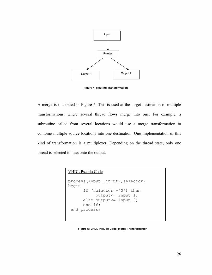
Figure 4: Routing Transformation
A merge is illustrated in Figure 6. This is used at the target destination of multiple
transformations, where several thread flows merge into one. For example, a
subroutine called from several locations would use a merge transformation to
combine multiple source locations into one destination. One implementation of this
kind of transformation is a multiplexer. Depending on the thread state, only one
thread is selected to pass onto the output.
Figure 5: VHDL Pseudo Code, Merge Transformation
VHDL Pseudo Code
process(input1,input2,selector) begin if (selector ='0') then output<= input 1; else output<= input 2; end if; end process;
Output 2
Router
Input
Output 1
26

Figure 6: Merge Transformation
In general, some threads may attempt to use the same resources at the same time,
causing deadlock, thus some sort of flow-control is necessary. One adequate approach
is to use a simple control mechanism involving a valid bit and pause signal. A valid
bit and a pause signal are associated with all incoming thread. The valid bit defines
whether the signal carries some valid data or not. When a transformation such as
merge cannot accept a thread, the pause signal is asserted. Naturally some kind of
logic must be used for these pause signals, and if used in a cycle, then must be used
carefully to avoid deadlock.
4.3 Dual Transformations
In this subsection we describe the dual transformation, which we believe is a novel
structure, and is the technology that enables us to model re-entrant concurrent
hardware threads with complex control structures found in most programming
languages.
Input 1 Input 2
Router
Output
27

Dual Transformations are difficult to describe in abstract, so it is best to
illustrate with several examples.
Examples of Dual transformations
Consider the case in which a thread is going to invoke a function or subroutine (see
Figure 7). To do this the thread is placed at the input of port A. The active thread state
is placed on the stack via a RAM write. At the output of port A, a new thread is
created which contains the parameters to the function and some return information,
such as the address of the RAM where the entry was stored, say r. This is analogous
to the Call machine instruction found o nearly all microprocessors. After performing
the transformations in the subroutine, the thread is routed to the input of port B. The
calling thread is retrieved from the “stack” through a RAM read according to the
value of r. The state of the thread is appended with the function return value and is
emitted at the output of port B. This is analogous to the Return machine instruction.
The thread then continues its path of execution. In this transformation the use of port
A and port B can occur simultaneously.
28
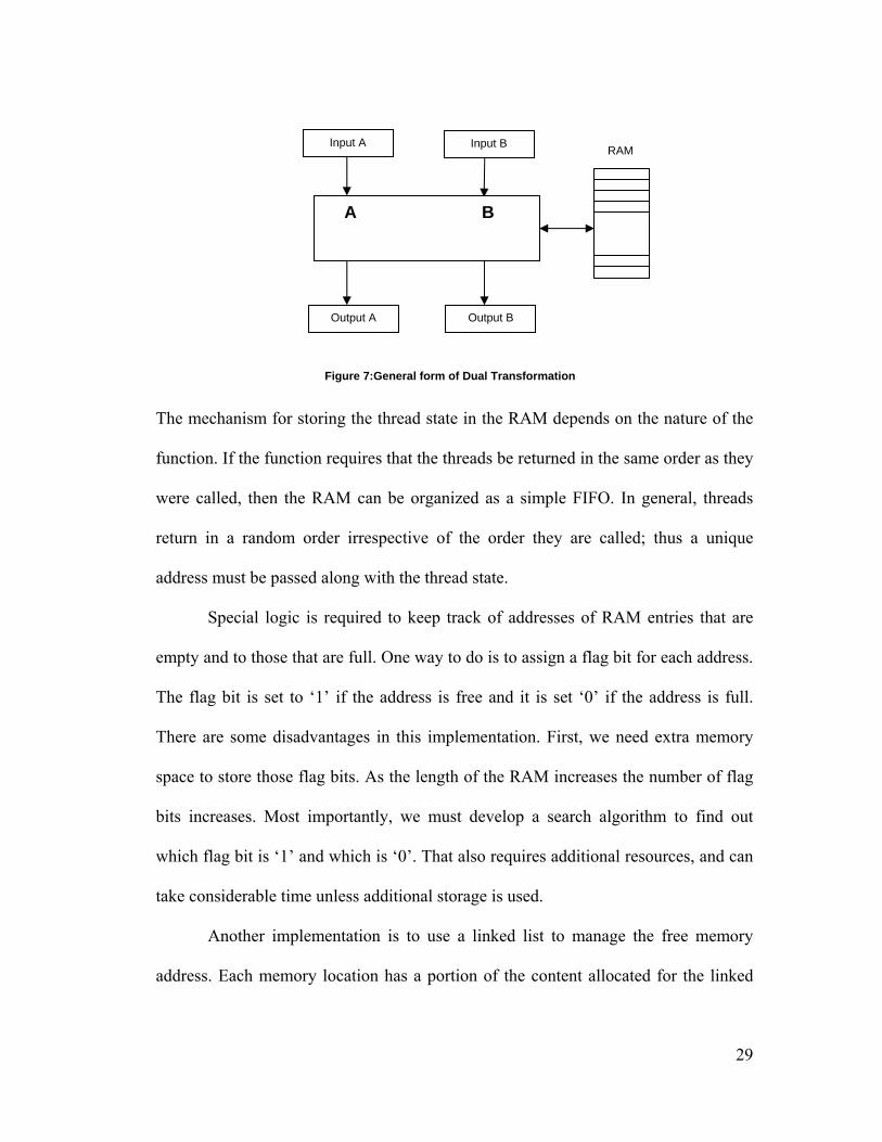
The mechanism for storing the thread state in the RAM depends on the nature of the
function. If the function requires that the threads be returned in the same order as they
were called, then the RAM can be organized as a simple FIFO. In general, threads
return in a random order irrespective of the order they are called; thus a unique
address must be passed along with the thread state.
Special logic is required to keep track of addresses of RAM entries that are
empty and to those that are full. One way to do is to assign a flag bit for each address.
The flag bit is set to ‘1’ if the address is free and it is set ‘0’ if the address is full.
There are some disadvantages in this implementation. First, we need extra memory
space to store those flag bits. As the length of the RAM increases the number of flag
bits increases. Most importantly, we must develop a search algorithm to find out
which flag bit is ‘1’ and which is ‘0’. That also requires additional resources, and can
take considerable time unless additional storage is used.
Another implementation is to use a linked list to manage the free memory
address. Each memory location has a portion of the content allocated for the linked
Input A Input B
A B
Output A
RAM
Output B
Figure 7:General form of Dual Transformation
29
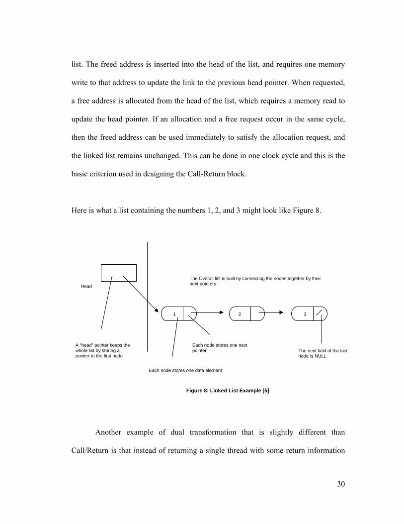
list. The freed address is inserted into the head of the list, and requires one memory
write to that address to update the link to the previous head pointer. When requested,
a free address is allocated from the head of the list, which requires a memory read to
update the head pointer. If an allocation and a free request occur in the same cycle,
then the freed address can be used immediately to satisfy the allocation request, and
the linked list remains unchanged. This can be done in one clock cycle and this is the
basic criterion used in designing the Call-Return block.
Here is what a list containing the numbers 1, 2, and 3 might look like Figure 8.
1 2 3
The Overall list is built by connecting the nodes together by their next pointers. Head
Each node stores one data element
Each node stores one next pointer The next field of the last
node is NULL
A “head” pointer keeps the whole list by storing a pointer to the first node
Figure 8: Linked List Example [5]
Another example of dual transformation that is slightly different than
Call/Return is that instead of returning a single thread with some return information
30

many threads are returned. One thread invokes the subroutine by placing an active
thread state at the input of port A, it is placed in the stack but instead of one thread
being omitted from the output of port A, a number of threads are emitted. After all
these threads complete they return at the input of port B and only one thread that was
placed on the stack is emitted out and continues its path of execution. This is
analogous to a DOALL statement, which facilitates parallelism.
Another use of dual transformation is FIFO pipes for message passing. Messages are
added through one port of the FIFO and removed from another. Special care must be
taken when considering the boundary conditions, such as when a thread writes to a
full-queue and when a thread reads from an empty queue.
Another example of dual transformation is in interprocess communication with
mailboxes. A sender can leave a message for a receiver in a particular mailbox
through a RAM write and the corresponding receiver can retrieve its message from
that mailbox through a RAM read. An example of message passing dual
transformation (Send- Receive block) is described in Section 6.3.3.2.
The blocking I/O transformation is an unusual type of dual transformation.
When a blocking I/O operation is requested at the input of port A, the thread is placed
on the stack and instead of a new thread being issued on the output of port A, an I/O
request is sent. When the reply to the I/O request is received at the input of the port B,
the thread is removed from the stack, combined with the results of the I/O operation
and emitted out from output of port B. That requires some way of associating the I/O
response with the thread ID making the request, which is often the case.
31

The dual transformations can be used for semaphores. A register within the
semaphore transformation may hold the value of the semaphore and a RAM can be
used to hold the state of blocked thread. A WAIT and POST command corresponds to
threads entering ports A and B. When a thread enters the input of port A it issues a
WAIT command and checks the state of the semaphore in the register. If the
semaphore is free then the thread continues its path of execution. If the semaphore is
in use by some other thread, then the thread is placed on the RAM. The entering of
the thread at the input of port B causes the POST command to be issued and
depending on the return information, a blocked thread is retrieved from the RAM and
emitted at the output of port B.
4.4 FIFO Transformations
The last transformations we discuss are the FIFO transformations. Since the registers
are limited in capacity, it may sometimes make sense to store the thread state in RAM
when it is inactive; i.e. is when it is not being used.
The FIFO transformations just like the route transformations do not change
the thread state. Figure 9 illustrates the FIFO transformations. If a part of a thread is
inactive, that is it does not read or write, it is a waste of resources to carry it further
through various transformations so it is placed in a FIFO and when the other part of
the thread completes its transformations, the inactive part of the thread is removed
32
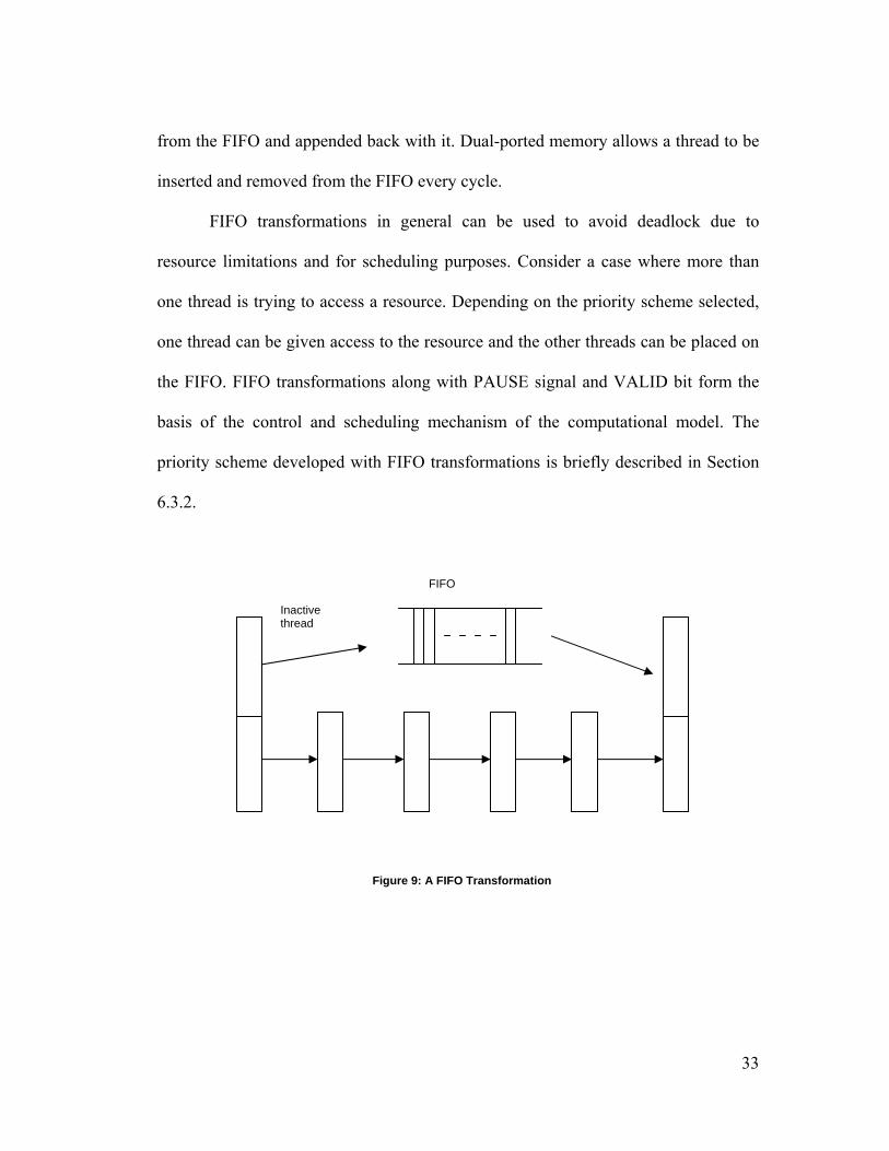
from the FIFO and appended back with it. Dual-ported memory allows a thread to be
inserted and removed from the FIFO every cycle.
FIFO transformations in general can be used to avoid deadlock due to
resource limitations and for scheduling purposes. Consider a case where more than
one thread is trying to access a resource. Depending on the priority scheme selected,
one thread can be given access to the resource and the other threads can be placed on
the FIFO. FIFO transformations along with PAUSE signal and VALID bit form the
basis of the control and scheduling mechanism of the computational model. The
priority scheme developed with FIFO transformations is briefly described in Section
6.3.2.
FIFO
Figure 9: A FIFO Transformation
Inactive thread
33
Chapter 5
Factorial
In this Chapter, we present a small example, a recursive computation of factorial. We
begin by describing the algorithm in high-level language and then describe the model
of computation.
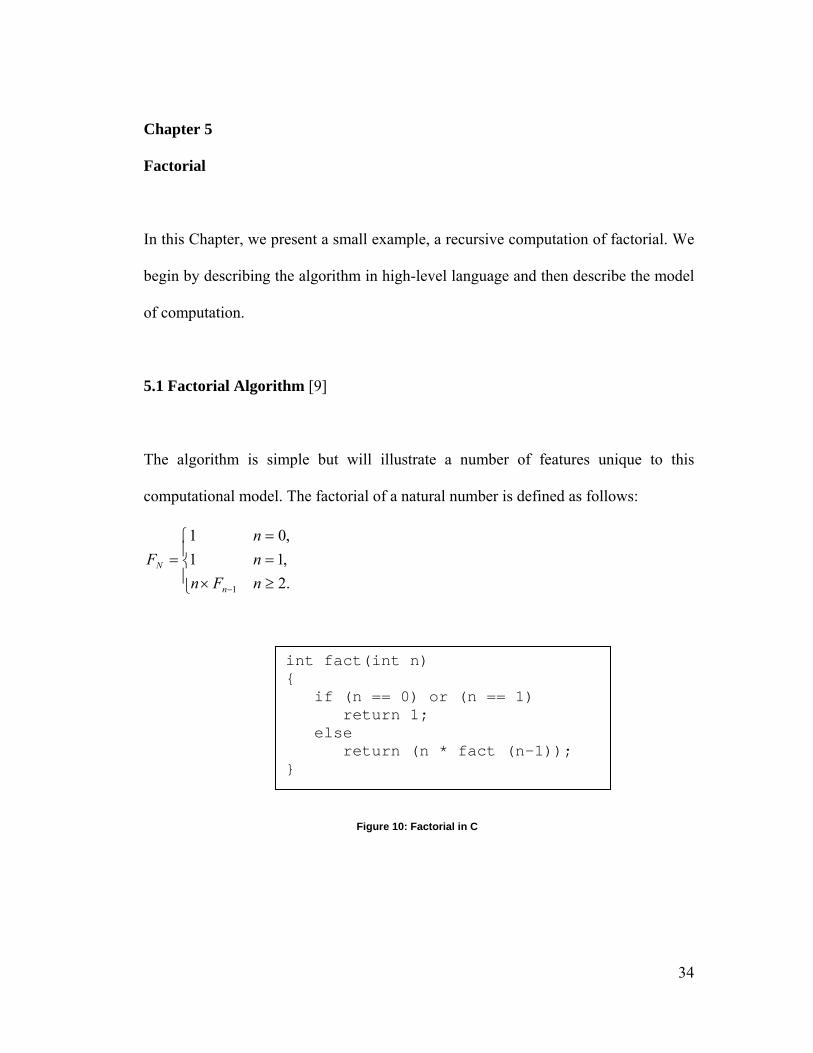
5.1 Factorial Algorithm [9]
The algorithm is simple but will illustrate a number of features unique to this
computational model. The factorial of a natural number is defined as follows:
⎪⎩
⎪⎨
⎧
≥×==
=
− .2,11,01
1 nFnnn
F
n
N
int fact(int n) { if (n == 0) or (n == 1) return 1; else return (n * fact (n-1)); }
Figure 10: Factorial in C
34
A naïve implementation of the factorial function is given above and is an example
often used to teach recursion. It is for that purpose that we selected to implement the
factorial function in our computational model.
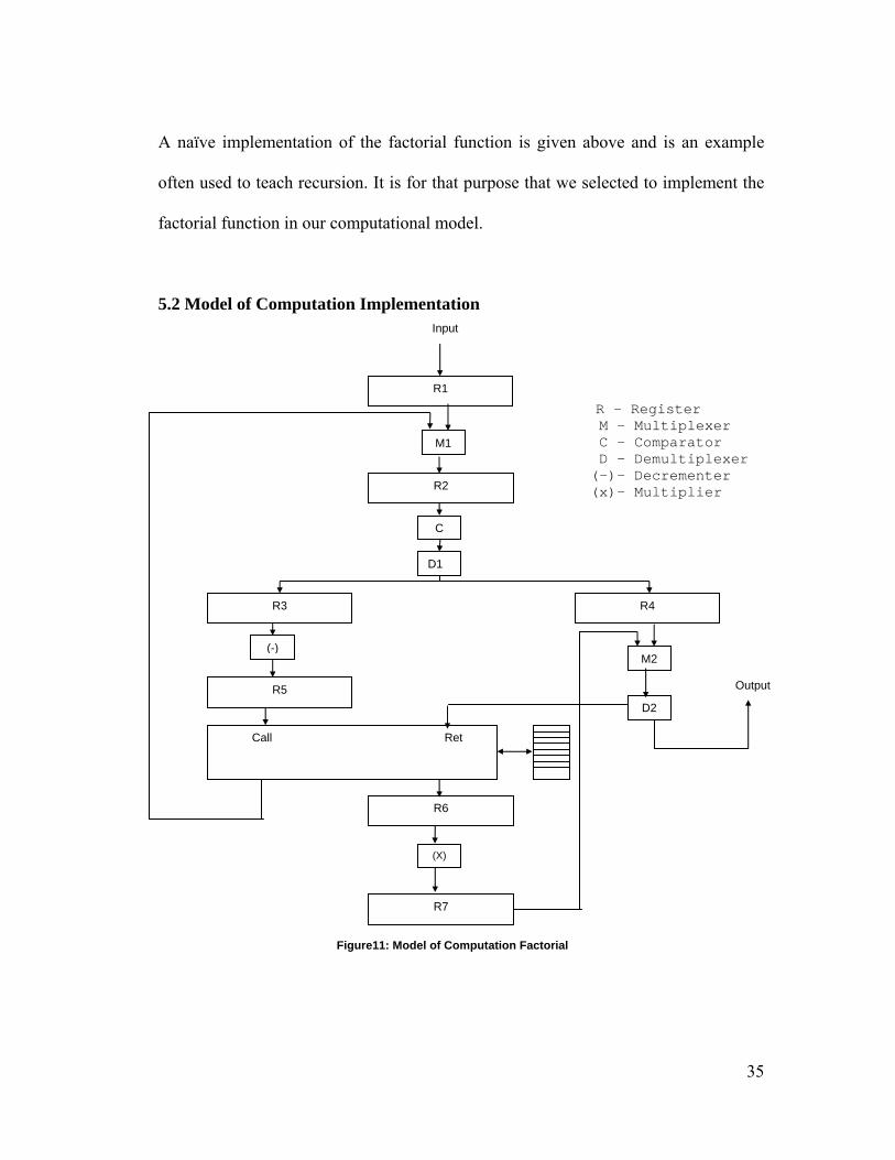
5.2 Model of Computation Implementation Input
R1
R5
Call Ret
C
D1
(-) M2
D2
(X)
R7
R2
R4 R3
R6
Output
R - Register M - Multiplexer C - Comparator D - Demultiplexer (-)- Decrementer (x)- Multiplier
M1
Figure11: Model of Computation Factorial
35

Figure 11 graphically represents a high-level view of our implementation of the
computation for the factorial function. In this section we will describe how it works.
Placing a valid thread on the input line labeled inputdata performs the call to the
function fact. The line inputdata is a bus that consists of data bits and control bits.
The data bits contain the return address information and the value to compute, x and
the valid bit. The line labeled outputdata returns the computation result.
When a thread enters the module, it first passes through a router; M1,
described in the Section 5.3.2.1.Which thread is chosen by the router depends on the
scheduling policy (blocking priority). Scheduling policies are described in detail in
Section 5.4. Once the thread is emitted from M1, it is placed in a register R1. In the
next cycle, the thread undergoes a test for x Є {0, 1, 2} and the boolean result s is
passed to another router. Depending on the value of s the router routes the thread to
the right (s=0) or to the left (s =1).
We need to follow two potential execution paths, one when s=0 and the other
when s=1.When s =0 the algorithm is trivial. The value that is returned is nothing but
the same value of computation, x. When s=1, then x > 2 and the algorithm is no
longer trivial. A part of the thread that contains x is passed through a decrementer and
the decremented value is appended to the thread. This thread then enters a dual
transformation and invokes a subroutine call. The databus of the thread is placed on
the RAM and a new thread is emitted out containing return information and the new
value of computation. This process repeats until s=0 and the thread is routed the other
way (left). The thread then invokes the return function. The thread carries some return
36

information (return address) with it. This return information is used to retrieve the
stored thread. The returned data is passed through a multiplier (x) and the product is
stored in a register R7. This thread again invokes the return function. This continues
until all the threads associated with a value of computation are retrieved, multiplied
and the result obtained. Then the thread containing the result is sent out at the output
port of the model.
5.3 Model of Computation: Building Blocks
The basic blocks in this program are registers, multiplexers, demultiplexers and the
call-return block. Of all these building blocks the call-return block is the most
significant one and allows us to fully implementing recursion. We will discuss each
of these modules in detail in this subsection.
5.3.1 Examples of Simple Transformations
In this subsection we describe some of the examples of simple transformations, which
we used in the Factorial program.
37
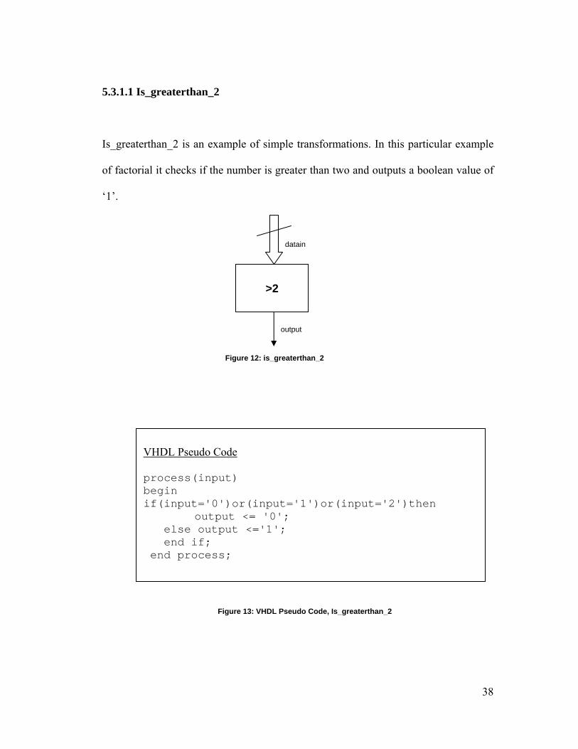
5.3.1.1 Is_greaterthan_2
Is_greaterthan_2 is an example of simple transformations. In this particular example
of factorial it checks if the number is greater than two and outputs a boolean value of
‘1’.
output
>2
datain
Figure 12: is_greaterthan_2
VHDL Pseudo Code process(input) begin if(input='0')or(input='1')or(input='2')then
output <= '0'; else output <='1'; end if; end process;
Figure 13: VHDL Pseudo Code, Is_greaterthan_2
38

5.3.1.2 Decrementer
Decrementer is also an example of simple transformation. The input is decremented
by one and transformed to the output.
Figure 15: VHDL Pseudo Code, Decrementer
Figure 15: VHDL Pseudo Code, Decrementer
dataout
datain
(- 1 )
underflow_error
Figure 14: Decrementer
VHDL Pseudo Code
process(input) begin if(input='0')then underflow_error <= '1'; else output <= input - '1'; end if; end process;
39

4.3.1.3 Multiplier
Another example of simple transformations is the multiplier. The two inputs are
multiplied and their product is transformed to the output.
Output
Multiplier
Input 2
Input 1
Figure 16: Multiplier
VHDL Pseudo Code
output <= input 1 * input 2;
Figure 17: VHDL Pseudo Code, Multiplier
40

5.3.2 Examples of Routing Transformations
5.3.2.1 Multiplexers
Multiplexers are basically selection devices. It is an example of routing
transformations Depending on the thread state, only one thread is selected to pass
onto the output.
Fi Figure 19: VHDL Pseudo Code, Multiplexer
Figure 18: Multiplexer
Output
Multiplexer
Input 1 Input 2
Selector
VHDL Pseudo Code
process(input 1,input 2,selector) begin if (selector ='0') then output <= input 1; else output <= input 2; end if; end process;
41

5.3.2.2 Demultiplexers
Demultiplexer is another example of routing transformations. Depending on the
condition the input is routed to one output or another.
Figure 21: VHDL Pseudo Code, Demultiplexer
Output 1
Demultiplexer
Input
Selector
Output 2
Figure 20: Demultiplexer
VHDL Pseudo Code
process(input,selector) begin if (selector ='0') then output 1 <= input; else output 2 <= input; end if; end process;
42

5.3.3 Example of Dual Transformations
5.3.3.1 Call-Return Block
In the factorial program, the call-return block is the most significant block and is an
ideal example for dual transformation. The data placed on the input line of the call is
written on the RAM and a new thread is emitted out containing return information
and the new value of computation. A thread with some return information is placed
on the input of the return function. This return information is used to retrieve the
stored data from the RAM.
Call Return
Figure 22: Call-Return Block
As discussed in Chapter 4, an efficient way to implement this design is to implement
the RAM as a linked list. The RAM used in this design is a single port distributed
select RAM.
The following are characteristics of the Distributed SelectRAM [1]
• A write operation requires only one clock edge.
43
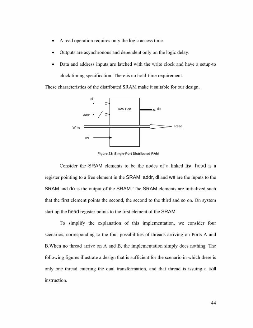
• A read operation requires only the logic access time.
• Outputs are asynchronous and dependent only on the logic delay.
• Data and address inputs are latched with the write clock and have a setup-to
clock timing specification. There is no hold-time requirement.
These characteristics of the distributed SRAM make it suitable for our design.
di
Consider the SRAM elements to be the nodes of a linked list. head is a
register pointing to a free element in the SRAM. addr, di and we are the inputs to the
SRAM and do is the output of the SRAM. The SRAM elements are initialized such
that the first element points the second, the second to the third and so on. On system
start up the head register points to the first element of the SRAM.
To simplify the explanation of this implementation, we consider four
scenarios, corresponding to the four possibilities of threads arriving on Ports A and
B.When no thread arrive on A and B, the implementation simply does nothing. The
following figures illustrate a design that is sufficient for the scenario in which there is
only one thread entering the dual transformation, and that thread is issuing a call
instruction.
R/W Port do addr
Write Read
we
Figure 23: Single-Port Distributed RAM
44
we SRAM di do addr
Head
call_data
call output address
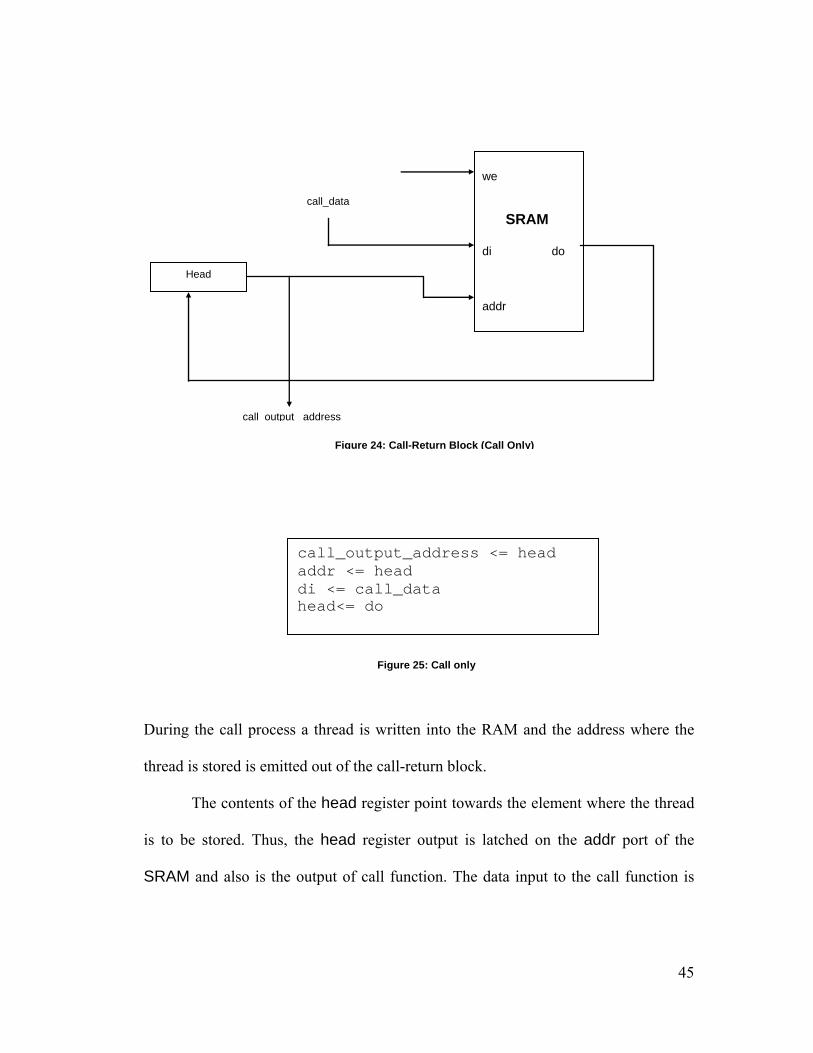
Figure 24: Call-Return Block (Call Only)
call_output_address <= head addr <= head di <= call_data head<= do
Figure 25: Call only
During the call process a thread is written into the RAM and the address where the
thread is stored is emitted out of the call-return block.
The contents of the head register point towards the element where the thread
is to be stored. Thus, the head register output is latched on the addr port of the
SRAM and also is the output of call function. The data input to the call function is
45

latched on the di port of the SRAM and the do of the SRAM updates the head
register, i.e., now head points to the next free address.
Figures 26 and 27 illustrate the scenario where a thread enters the dual
transformation, Call-Return Block and invokes a return instruction.
we SRAM di do addr
Head
return_data
return_input_address
Figure 26: Call-Return Block (Return Only)
addr<= return_input_address return_data<= do di<=head head<= return_input_address
Figure 27: Return Only
During the return process a thread with some return information is placed on the input
of the return function and this information is used to retrieve the stored thread.
The return_input address is latched on the addr port of the SRAM and the
data read from the port do is placed on the signal return data. The contents of the
46
head register are latched on the di port and then it is updated with the return input
address.
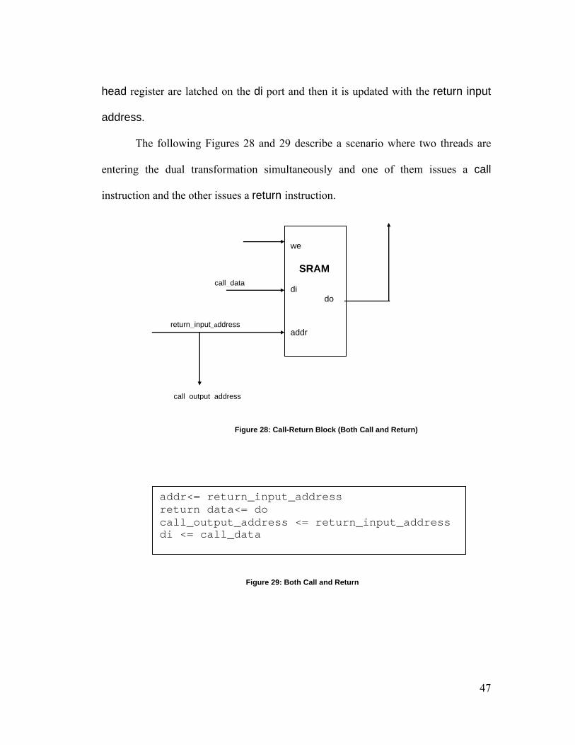
The following Figures 28 and 29 describe a scenario where two threads are
entering the dual transformation simultaneously and one of them issues a call
instruction and the other issues a return instruction.
we SRAM di
do addr
call_data
return_input_address
call_output_address
Figure 28: Call-Return Block (Both Call and Return)
addr<= return_input_address return data<= do call_output_address <= return_input_address di <= call_data
Figure 29: Both Call and Return
47

When both call and return take place at the same time a thread is written into the
RAM and the address is emitted out of the call output port. Simultaneously at the
return output port a stored thread is retrieved.
This is one of the simplest cases of Call-Return. The address from which the
stored thread is retrieved is written into during the call process. Both the call and the
return simultaneously are possible in one clock cycle because of the use of
Distributed Select RAM.
The return_input address is latched on the addr port of the SRAM and the data
read from the port do is placed on the signal return data. The call data is latched on
the di port of the SRAM. Since the recently freed element is written to the call
output address is same as the return input address.
Figure 30 shows the hardware of the Call-Return Block. return_data
call_ output_address
0 mux
mux
mux
mux
Head 01
1
0
10
1
Head in
Head out
call_data
return_input_ address
we SRAM di do addr
Figure 30: Call-Return Block
48

5.4 Scheduling and Control Logic
Deadlocks can be caused when more than one thread competes for the use of a
transformation. Prudent use of FIFO and good capacity planning can be used to avoid
deadlock. In the discussion below, we have assumed that deadlocks occur only
because of capacity limitations but there are many other reasons that cause deadlocks
such as incorrect programming and software faults in the compiler.
Deadlocks depend on the scheduling policies used in the transformations
particularly the routing transformations. For the factorial example described in
Section 5.2, a scheduling policy is required at the two routers, M1 and M2 where
there is a possibility that more than one thread can compete for its use.
A round robin strategy would guarantee fairness, but might cause exponential
growth in the number of threads. Another strategy is to give preference to one source
of threads over the other. We have implemented the scheduling in the routers in such
a way that only one thread is given priority and the other thread must wait for the first
thread to run to completion. These routers are called blocking priority routers, since
one thread is given priority over the other and the lower priority thread is blocked.
Another technique to resolve priority is to use non-blocking priority routers. Non-
blocking priority routers use a FIFO to store the lower priority thread. We discuss
this technique in detail in Section 6.3.2.1.
The Factorial program utilizes the valid/pause signals to manage control flow
between connected transformations and registers. When a transformation or a register
49

is in use by one thread and another thread tries to access it a Pause signal is asserted
by the transformation to the new thread asking it to hold and wait till it is free to
accept it. If all the transformations are asserting a Pause signal, the system goes into
deadlock.
50
Chapter 6
Fibonacci
In this chapter, we begin with a brief introduction to the Fibonacci algorithm in
Section 6.1 and then proceed to describe the model of computation in Section 6.2 and
the building blocks in Section 6.3.
6.1 Fibonacci Algorithm [9]
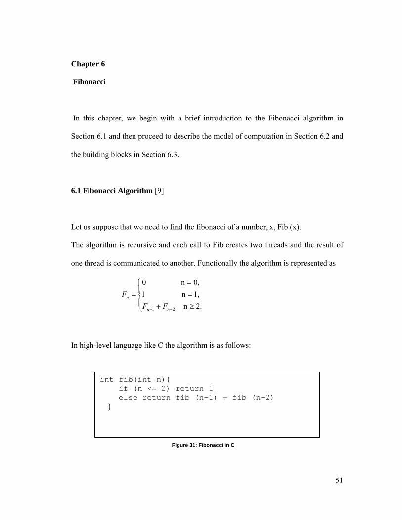
Let us suppose that we need to find the fibonacci of a number, x, Fib (x).
The algorithm is recursive and each call to Fib creates two threads and the result of
one thread is communicated to another. Functionally the algorithm is represented as
⎪⎩
⎪⎨
⎧
≥+==
=
−− 2.n 1,n 10,n 0
21 nn
n
FFF
In high-level language like C the algorithm is as follows:
int fib(int n){ if (n <= 2) return 1
else return fib (n-1) + fib (n-2) }
Figure 31: Fibonacci in C
51
This algorithm is modeled closely after the recursive definition. Implementation of
the model of computation of fibonacci is more complex than the factorial because the
fibonacci function refers to itself twice.
6.2 Model of Computation Implementation
Figure 32 illustrates the graphical implementation of the model of computation for the
fibonacci program. Placing a valid thread on the input line labeled inputdata
performs the call to the function fib. The line is a bus, which consists of data bits and
control bits. The data bits contain the return address information and the value to
compute, x and also specify whether the thread is valid or not. The line labeled
outputdata returns the computation result.
When the thread enters the module, it first passes through a blocking priority
router, called BP. Once the thread is emitted from BP, it passes through a non-
blocking priority router(NBP1) and then the selected thread is placed in a register
R1. In the next cycle, the thread undergoes a test for x Є {1, 2} and the boolean result
s is placed to another router. Depending on the value of s the router routes the thread
to the right (s=1) or to the left(s=0).
If s=1, then neither the value of x nor the value of s are relevant, so they are
simply dropped. For illustration, we show that a register is used to contain the value
1, but in practice, this could be hard coded into that portion of the thread state.
Next, the thread competes with another thread for the services of another 2-3
router. It is likely that preference is given to this thread. Based on part of the return
52
information r.dest, the thread is routed to the transformation that issued the call. The
return information ‘r’ is made up of two fields: r.dest and r.index. The router uses
r.dest to route to the calling information. The field r.index may be used by the
calling transformation to look up the calling thread state in a RAM. We’ll discuss this
shortly.
Backing up to D1, if s=0, then x>2 and the algorithm is no longer trivial.
First, the thread enters a dual transformation to get a communication channel. The
communication block is explained in Section 5.3.3.1. If none are available, the thread
blocks. The dual transformation uses the RAM labeled stk. Once a communication
channel is received, the value of the channel is given by p, and the thread state is
augmented to hold this value. The left port of the dual transformation performs the
function get_pipe_channel ( ).
Next, the thread forks into two threads. Note that for illustration we show this
happening in one cycle, but in fact this can be performed in the same cycle that shows
the previous transformation. Now there are two threads with nearly identical states.
We label these threads, left and right based on their position in the figure. The left
thread does not have the value r because analysis shows that the thread does not
return, so r is never referenced, and thus it may be dropped. The thread on the right
does eventually return, so that thread retains the value of r.
Both threads then perform a subtraction and place the result in a temporary
variable. The value of x is no longer used, so the threads no longer need to maintain
its value. Next, both the threads call fib and pass the parameters x-1 and x-2. The
53

only state that needs to be in the left stack is the value of p and the states that need to
be stored in the right stack are the values of p and r. On the left, the value r.dest is set
to 1, which is the unique return value for this particular transformation, and the index
of the array in which p is stored is emitted in r.index. When the thread returns, the
value r.index is used to match the return value, stored in t2, with the communication
channel p. A similar event happens to the right, with r.dest set to 2.
Once the left thread return, the return value (t2) is sent via a mailbox p. Use of
get_pipe_channel ( ) ensures that the channel will be empty. Once the message is
sent, the thread terminates. On the right, the return value is also placed in t2, and then
the thread tries to read the value sent through mailbox p. If no value is sent, the thread
is stored on the stack in location p. Once the message is sent, the dual transformation
emits the thread together with the received message placed in t3. In the next step the
thread releases the communication channel. When that’s complete, the two values t2
and t3 are added. When the addition is complete, the result is stored in t4 and the
value is returned.
54

i
Figure 32: Model of Computation Fibonacc
55
6.3 Program of Computation: Building Blocks
The basic blocks in this program of computation are registers, multiplexers,
demultiplexers, adders, the call-return block, the communication block, non-blocking
priority routers and the send-receive block. Of all these building blocks the send-
receive block has not yet been discussed and is an ideal example of message passing
dual transformation.
Registers, multiplexers, demultiplexers and decrementers were discussed in Chapter
5.We will discuss the remaining blocks in this subsection.
6.3.1 Examples of Simple Transformations
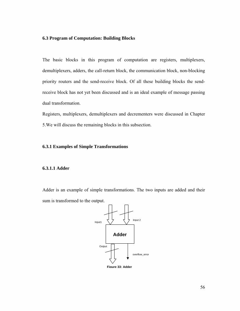
6.3.1.1 Adder
Adder is an example of simple transformations. The two inputs are added and their
sum is transformed to the output.
Figure 33: Adder
Output
Adder
Input 2
overflow_error
Input1
56

VHDL Pseudo Code
process(input1,input2) begin output_temp <= input1 + input2; end process; process(input1,input2) begin if(input1=/’0’)and (input2=/’0’) then if(output_temp =’0’) then overflow_error<=’1’; else overflow_error<=’0’; end if; end if; end process; output<=output_temp;
Figure 34: VHDL Pseudo Code, Adder with Overflow Error Check
6.3.2 Examples of Routing Transformations
6.3.2.1 Non-Blocking Priority Router
In Chapter 5, we described a scheduling policy where, if more than one thread tries to
access a routing transformation, we give priority to one of the threads over the other
thread. The routing transformation is hence called a blocking priority router. However
this might lead to computational errors. To avoid this kind of error we suggest
another kind of a router, which has a FIFO along with the router. This is called the
57

non-blocking priority router. In this router the thread that is given the higher priority
is routed to the next transformation and the one thread that has a lower priority is
placed in the FIFO.
The scheduling policy used by us is given in the following VHDL code. Consider the
two inputs of the ROUTER to be input1, input2 and FIFOOUT and the outputs to
be output and FIFOIN.
VHDL Pseudo Code
OUTPUT_Selection:process(select,input1,input2,FIFOOUT)begin case select is when "000" =>output<=(others=>'0'); when "001" =>output<= FIFOOUT; when "010" =>output<= input2; when "011" =>output<= input2; when "100" =>output<= input1; when "101" =>output<= input1; when "110" =>output<= input1; FIFOIN <=input2; when "111" =>FIFOIN <=input2; output<= input1; when others=>NULL; end case; end process;
Figure 35: VHDL Pseudo Code, Non-Blocking Priority Router
58

FIFO
Output
ROUTER
n Fifoout
Fifoin n
n
nn
Input 2 Input 1
select
FIFO
Figure 3 6: Non-Blocking Priority Router
6.3.3 Example of Dual Transformations
6.3.3.1 Communication Block
In the fibonacci program, the communication block is one of the most significant
blocks and is a good example for dual transformation. On a request instruction a
channel number is emitted out of request port and on a release instruction a channel is
released.
59

Request Release
Figure 37: Communication Block
This block is similar to the Call-Return Block discussed in Chapter 5.Consider
the SRAM elements to be the nodes of a linked list. head is a register pointing to the
free element in the SRAM. addr, di and we are the inputs to the SRAM and do is the
output of the SRAM. Data is read from the SRAM only when there is a thread issuing
a request instruction. The SRAM elements are initialized such that the first element
points the second, the second to the third and so on. On system start up the head
register points to the first element of the SRAM.
Figures 38 and illustrate the scenario where a thread issues a request and no thread
issues a release.
we SRAM di do addr
Head
channel number Figure 38:Communication Block (Request Only)
60

Channel_number<= head addr <= head head<= do
Figure 39:Request Only
During the request process a channel_number is emitted out of the communication
block.The value of the head register points towards the first free element of the
RAM. The head register output is the output of request function. The do of the
SRAM updates the head register, i.e., now head points to the next free address.
Next we consider a case in which no thread requests a channel and one thread
releases a channel. This is shown in Figures 40 and 41.
head
release_channel
we SRAM di do addr
Figure 40: Communication Block (Release Only)
61
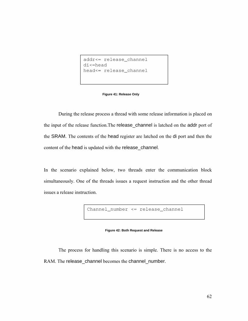
addr<= release_channel di<=head head<= release_channel
Figure 41: Release Only
During the release process a thread with some release information is placed on
the input of the release function.The release_channel is latched on the addr port of
the SRAM. The contents of the head register are latched on the di port and then the
content of the head is updated with the release_channel.
In the scenario explained below, two threads enter the communication block
simultaneously. One of the threads issues a request instruction and the other thread
issues a release instruction.
Channel_number <= release_channel
Figure 42: Both Request and Release
The process for handling this scenario is simple. There is no access to the
RAM. The release_channel becomes the channel_number.
62

Figure 43 shows the hardware of the Communication Block.
0
mux
mux
muxmux
Head 10
1
0
1
0
1
Head in
Head out
channel data
release_channel
channel_number
we SRAM di do addr
Figure 43: Communication Block
6.3.3.2 Send-Receive Block
In the example of fibonacci design, the most significant block is the Send-Receive
block. This block is used for message passing and is an example of dual
transformations. The function of message system is to allow threads to communicate
among themselves in a more organized way than shared memory. Indirect
communication [6] is one of the ways in which threads that communicate refer to
each other. With indirect communication, the messages are sent to and received from
“mailboxes”. A mailbox is an object into which messages or threads can be placed
63

and from which messages and threads can be removed. Each mailbox has a unique
identification.
In our design this unique identification is called the channel number and is provided
by the communication block discussed before. Communication is possible between
two threads only if they share a mailbox. The Send and Receive primitive are
defined as follows:
Send (A, message) – Send a message to mailbox A
message=Receive (A) – Receive a message from mailbox A
Send Receive
Figure 44: Send-Receive Block
The mailbox is implemented using a Distributed SelectRAM, explained in
Section 6.3.3.1. The mailbox can be empty or full. At the system start-up the RAM
elements are empty and therefore are all initialized with all zeroes. The two least
significant bits of the data written into the RAM are the status bits and describe the
status of the data in the RAM that is whether it is empty or contains a message or
contains a thread. Figure 45 shows the status bits.
64
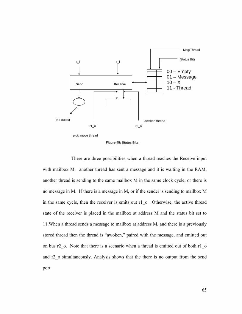
There are three possibilities when a thread reaches the Receive input
with mailbox M: another thread has sent a message and it is waiting in the RAM,
another thread is sending to the same mailbox M in the same clock cycle, or there is
no message in M. If there is a message in M, or if the sender is sending to mailbox M
in the same cycle, then the receiver is emits out r1_o. Otherwise, the active thread
state of the receiver is placed in the mailbox at address M and the status bit set to
11.When a thread sends a message to mailbox at address M, and there is a previously
stored thread then the thread is “awoken,” paired with the message, and emitted out
on bus r2_o. Note that there is a scenario when a thread is emitted out of both r1_o
and r2_o simultaneously. Analysis shows that the there is no output from the send
port.
Figure 45: Status Bits
Send Receive
r1_o
r_is_i Status Bits
00 – Empty 01 – Message 10 – X 11 - Thread
Msg/Thread
No output awaken thread r2_o
picknmove thread
65

Next, we describe the working of the Send/Receive block in detail under the scenario
where there is a sending thread and no receive thread.
we SRAM di do addr
1 0
empty
msg
LSB
Figure 46: Send-Receive Block (Send Only)
send( s.msg, s.addr) if ( M[s.addr].status == empty) then M[s.addr] <= s.msg M[s.addr].status <= msg else if ( M[s.addr].status == thread) then r2_o.msg <= s.msg r2_o.data<= M[s.addr].data M[s.addr].status <= empty else ERROR
Figure 47: Send Only
During the send process, depending on the status either a message is written
into the RAM for the receiver to receive, or a receiving thread previously stored by
the receiver is awaken, paired with the message and removed from the RAM. If there
66

is a previously stored message in the mailbox (status bits 01) then an error is
generated, when some other sending thread sends a message to it.
During the receive process depending on the status either a thread is written into the
RAM for the sender to awaken it or a message stored by the sender is retrieved out of
the RAM. This is illustrated in Figures 48 and 49.
we SRAM di do addr
1 0
empty
thread
LSB
Figure 48: Send-Receive Block (Receive Only)
receive(r.thread, r.addr) if (M[r.addr].status == empty) then M[r.addr] <= r.thread M[r.addr].status <= thread else if (M[r.addr].status == msg) then r1_o.msg<= M[r.addr].msg M[r.addr].status <= empty else ERROR
Figure 49: Receive Only
67
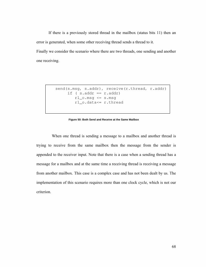
If there is a previously stored thread in the mailbox (status bits 11) then an
error is generated, when some other receiving thread sends a thread to it.
Finally we consider the scenario where there are two threads, one sending and another
one receiving.
send(s.msg, s.addr), receive(r.thread, r.addr) if ( s.addr == r.addr) r1_o.msg <= s.msg r1_o.data<= r.thread
Figure 50: Both Send and Receive at the Same Mailbox
When one thread is sending a message to a mailbox and another thread is
trying to receive from the same mailbox then the message from the sender is
appended to the receiver input. Note that there is a case when a sending thread has a
message for a mailbox and at the same time a receiving thread is receiving a message
from another mailbox. This case is a complex case and has not been dealt by us. The
implementation of this scenario requires more than one clock cycle, which is not our
criterion.
68

Figure 51 shows the hardware for the send-receive block.
0
mux
we
SRAM addr do
di
1
s.addr
1
0
r.addr1
0 empty
msg
1
0
empty
thread
ux m
mux
mux
Figure 51: Send-Receive Block
6.4 Capacity and Scheduling
In the Fibonacci program, the number of threads is exponential in the size of x, which
can quickly overwhelm the capacity of modern FPGAs. However, by studying the
behavior and straightforward use of transformations and thread scheduling, we can
easily manage the complexity and maintain high utilization of the system.
In our example, we have not provided the details for resolving competition
between recursive calls. In particular, the 3-1-merge transformation at the top of the
model needs to be defined. One possibility is a round robin approach, which
69
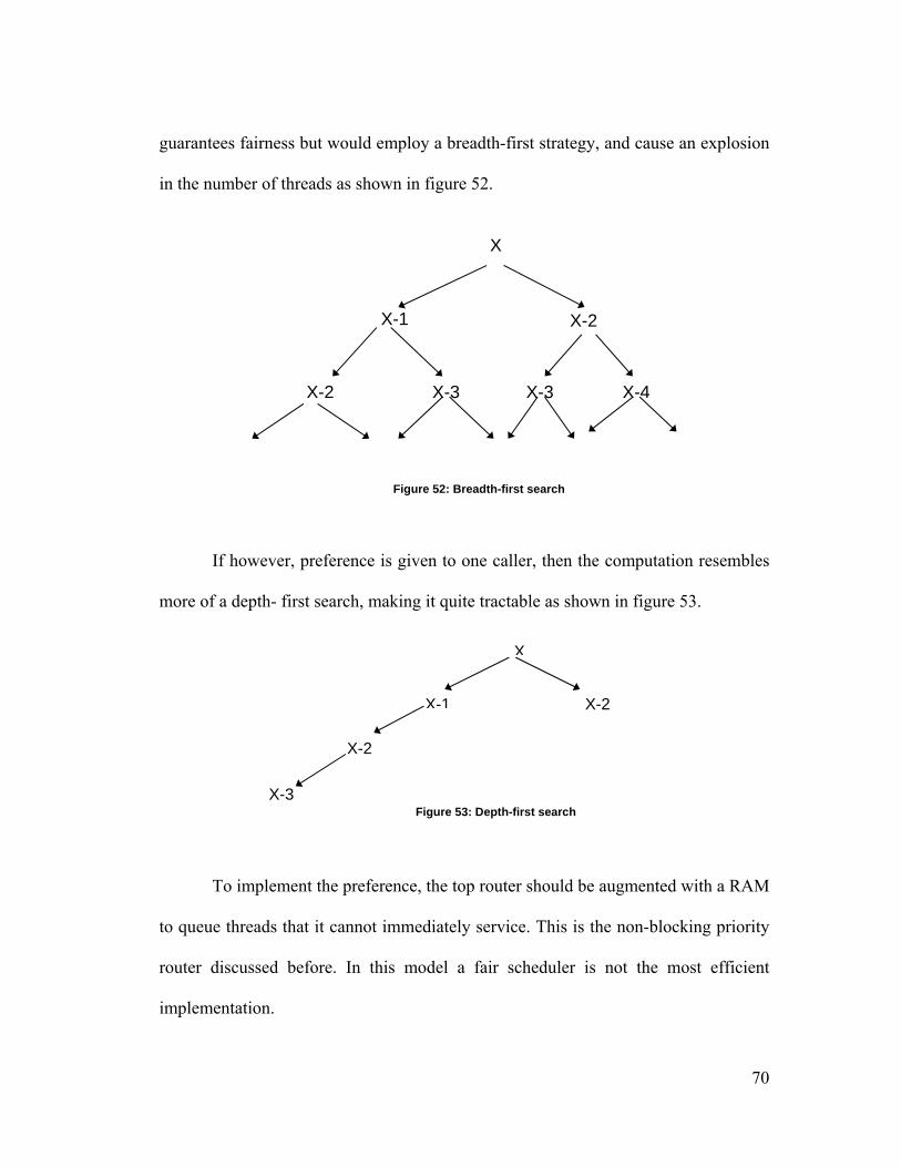
guarantees fairness but would employ a breadth-first strategy, and cause an explosion
in the number of threads as shown in figure 52.
X
X-1 X-2
X-2 X-3 X-3 X-4
Figure 52: Breadth-first search
If however, preference is given to one caller, then the computation resembles
more of a depth- first search, making it quite tractable as shown in figure 53.
X
X-2 X-1
X-2
X-3 Figure 53: Depth-first search
To implement the preference, the top router should be augmented with a RAM
to queue threads that it cannot immediately service. This is the non-blocking priority
router discussed before. In this model a fair scheduler is not the most efficient
implementation.
70
Chapter 7
Results and Future Work
In this chapter, we describe the simulation and synthesis results. The VHDL Code for
factorial and fibonacci is simulated using Modelsim XE II 5.8c and synthesized using
Xilinx ISE 6.3i.
7.1 Simulation Results
Table 1 shows the results from the factorial example. The column named input
indicates the values that are presented to the Factorial program. Note that the
implementation allows for multiple threads to be actively executing at the same time.
In the case where multiple threads were presented, we show the values and the cycle
number in which they start and end the program.
71

Input
Input Cycle Number
Output
Output Cycle Number
2 1 2 3 3 1 6 8 4 1 24 13 5 1 120 18 6 1 720 23 7 1 5040 28 8 1 40320 33 9 1 362880 38 10 1 3628800 43 1,7 1,2 1,5040 3,29 2,10 1,2 2,362880 3,44 1,8,2 1,2,3 1,2,40320 3,5,34 1,10,2,5 1,2,3,4 1,2,120,362880 3,5,21,44
Table 1: Factorial Results
Observations:
The time taken to obtain the factorial of a number is independent of the number of
threads. This is because of the scheduling policy used by us. We opted for blocking
priority in which a new thread is blocked until an old thread has completed its
execution.
Table 2 shows the results for the Fibonacci.
72
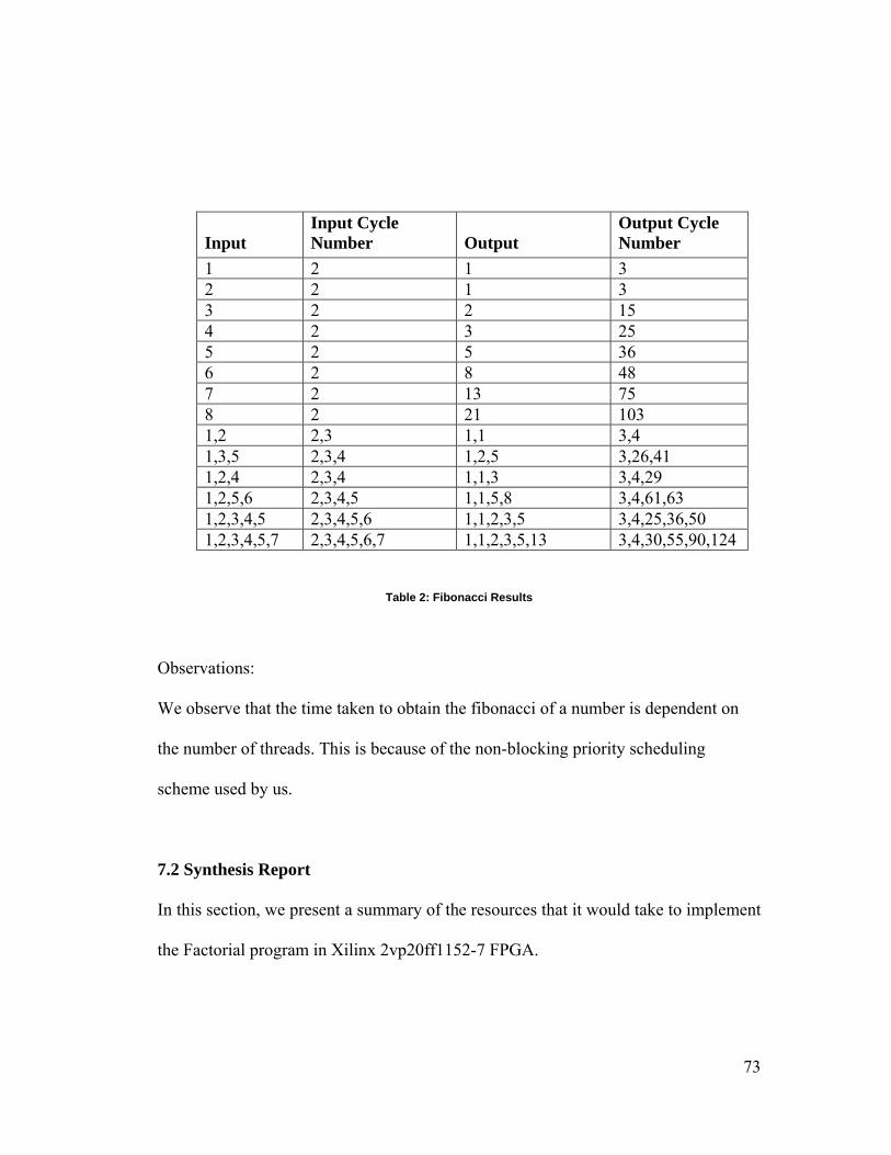
Input
Input Cycle Number
Output
Output Cycle Number
1 2 1 3 2 2 1 3 3 2 2 15 4 2 3 25 5 2 5 36 6 2 8 48 7 2 13 75 8 2 21 103 1,2 2,3 1,1 3,4 1,3,5 2,3,4 1,2,5 3,26,41 1,2,4 2,3,4 1,1,3 3,4,29 1,2,5,6 2,3,4,5 1,1,5,8 3,4,61,63 1,2,3,4,5 2,3,4,5,6 1,1,2,3,5 3,4,25,36,50 1,2,3,4,5,7 2,3,4,5,6,7 1,1,2,3,5,13 3,4,30,55,90,124
Table 2: Fibonacci Results
Observations:
We observe that the time taken to obtain the fibonacci of a number is dependent on
the number of threads. This is because of the non-blocking priority scheduling
scheme used by us.
7.2 Synthesis Report
In this section, we present a summary of the resources that it would take to implement
the Factorial program in Xilinx 2vp20ff1152-7 FPGA.
73
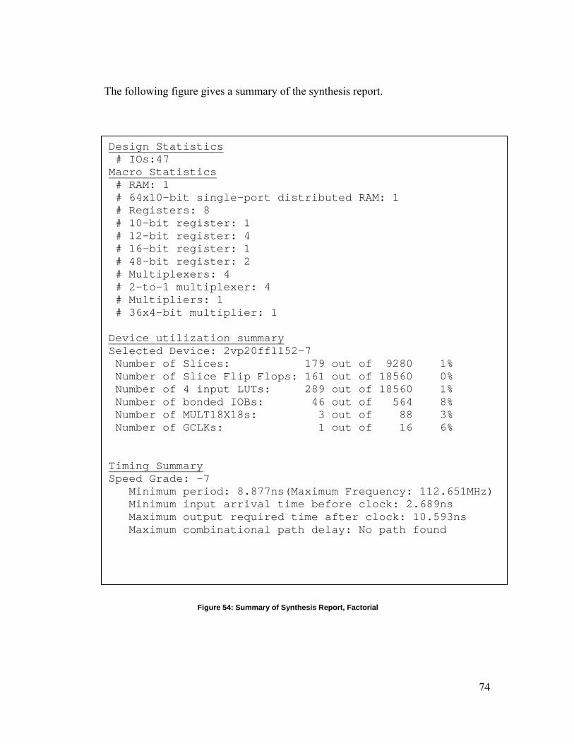
The following figure gives a summary of the synthesis report.
The following figure gives a summary of the synthesis report when the Fibonacci
program is synthesized for Xilinx 2vp20ff1152-7 FPGA.
Design Statistics # IOs:47 Macro Statistics # RAM: 1 # 64x10-bit single-port distributed RAM: 1 # Registers: 8 # 10-bit register: 1 # 12-bit register: 4 # 16-bit register: 1 # 48-bit register: 2 # Multiplexers: 4 # 2-to-1 multiplexer: 4 # Multipliers: 1 # 36x4-bit multiplier: 1 Device utilization summary Selected Device: 2vp20ff1152-7 Number of Slices: 179 out of 9280 1% Number of Slice Flip Flops: 161 out of 18560 0% Number of 4 input LUTs: 289 out of 18560 1% Number of bonded IOBs: 46 out of 564 8% Number of MULT18X18s: 3 out of 88 3% Number of GCLKs: 1 out of 16 6% Timing SummarySpeed Grade: -7 Minimum period: 8.877ns(Maximum Frequency: 112.651MHz) Minimum input arrival time before clock: 2.689ns Maximum output required time after clock: 10.593ns Maximum combinational path delay: No path found
Figure 54: Summary of Synthesis Report, Factorial
74
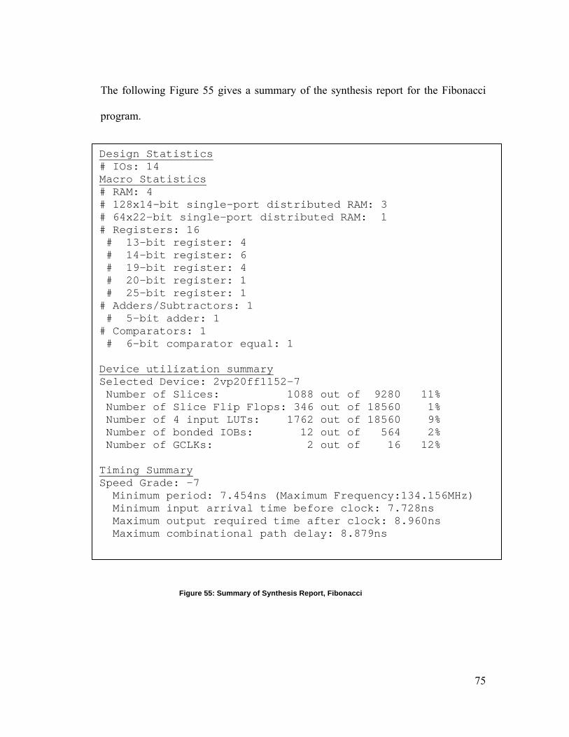
The following Figure 55 gives a summary of the synthesis report for the Fibonacci
program.
Design Statistics # IOs: 14 Macro Statistics # RAM: 4 # 128x14-bit single-port distributed RAM: 3 # 64x22-bit single-port distributed RAM: 1 # Registers: 16 # 13-bit register: 4 # 14-bit register: 6 # 19-bit register: 4 # 20-bit register: 1 # 25-bit register: 1 # Adders/Subtractors: 1 # 5-bit adder: 1 # Comparators: 1 # 6-bit comparator equal: 1 Device utilization summarySelected Device: 2vp20ff1152-7 Number of Slices: 1088 out of 9280 11% Number of Slice Flip Flops: 346 out of 18560 1% Number of 4 input LUTs: 1762 out of 18560 9% Number of bonded IOBs: 12 out of 564 2% Number of GCLKs: 2 out of 16 12% Timing SummarySpeed Grade: -7 Minimum period: 7.454ns (Maximum Frequency:134.156MHz) Minimum input arrival time before clock: 7.728ns Maximum output required time after clock: 8.960ns Maximum combinational path delay: 8.879ns
Figure 55: Summary of Synthesis Report, Fibonacci
75
7.3 Future Work
In the summary of the synthesis report we see that 11% of the CLBs were
used. This is number is quiet modest but can still be reduced by using
BlockRAM instead of Distributed SelectRAM.
The programs were limited to input sizes that were small. Increase in the input
size would increase the number of resources used.
The next step to improve this computational model will be to implement
pointers to functions to include memory management capabilities.
7.4 Conclusion
The Computational model developed by us has the following features
Fully recursive
Allows high-level concurrency
Implements complex constructs such as call-return subroutine and
message passing
Utilizes modest resources
There is now a computational model that allows reconfigurable logic to provide an
excellent base for design and implementation of various complex algorithms such as
genetic algorithms in hardware. The emerging high-level synthesis technology with
this computational model raises the level of abstraction for FPGA programming from
gate-level parallelism and will help the system designers to bridge the gap between
hardware and software.
76
Bibliography
1. Virtex-II Pro Platform FPGA Handbook
2. Streams-C. Webpage: http://www.streams-c.lanl.gov/index.shtml
3. Jan Frigo, Maya Gokhale, Los Alamos NationalLaboratory Dominique
Lavenier-
Luciano Lavagno Ellen Sentovich Cadence Berkeley Laboratories,” ECL: A
Specification Environment for System-Level Design”.
4. Handel-C. Webpage: http://www.celoxica.com/techlib/files/CEL-
W0307171L48-63.pdf
5. Linked List. Webpage: http://cslibrary.stanford.edu/103/LinkedListBasics.pdf
6. Silberschatz, Galvin and Gagne, Operating System Concepts, Sixth Edition
7. David Andrews, Douglas Niehaus, and Peter Ashenden, “Programming
Models for Hybrid FPGA/CPU Computational Components”. IEEE
Computer, January 2004
8. http://www.xilinx.com/
9. Yedidyah Langsam, Moshe J. Augenstein and Aaron M.Tenenbaum, Data
Structures Using C and C++, Second Edition
10. David Andrews, Douglas Niehaus, razali Jidin, Michael Finley, Wesley Peck,
Michael Frisbie, Jorge Ortiz, Ed Komp and Peter Ashenden, “Programming
Models for Hybrid FPGA-CPU Computational Components: A Missing
Link”, IEEE Micro, July/August 2004(Vol. 24, No.4), pp.42-53
77

11. Razali Jidin, David Andrews and Douglas Niehaus, “Implementing
Multithreaded System Support for Hybrid FPGA/CPU Computational
Components”,Pro.Int’l Conference On Engineering of Reconfigurable
Systems and Algorithms, CSREA Press, June 2004.pp. 116-122
12. Kavi Arya, “Handel-C: A New Paradigm in Embedded Systems”
13. Christian Peter, Oxford University Computing Laboratory, UK,“Overview:
Hardware Compilation and the Handel-C language”
14. www.celoxica.com
15. www.jhdl.com
16. www.systemc.org
78