comparison of nmos and pmos hot carrier effects from 300 to 77 k
TRANSCRIPT
268 IEEE TRANSACTIONS ON ELECTRON DEVICES, VOL. 44, NO. 2, FEBRUARY 1997
Comparison of NMOS and PMOS HotCarrier Effects From 300 to 77 K
Miryeong Song, Kenneth P. MacWilliams,Member, IEEE, and Jason C. S. Woo
Abstract—Since hot carrier effects can pose a potential limitto device scaling, hot-carrier-induced device degradation hasbeen one of the major concerns in modern device technology.Currently, there is a great interest in pursuing low-temperatureoperation of MOS devices since it offers many advantages com-pared to room temperature operation. Also, low-temperatureoperation is often required for space applications. However,low-temperature operation exacerbates hot carrier reliability ofMOS devices. Even though hot carrier effects are significantlyworse at low temperature, most of the studies on hot-carrier-induced device degradation were done at room temperatureand little has been done at low temperature. In this work,hot-carrier-induced device degradation is characterized from77 K to room temperature for both NMOS and PMOS deviceswith the emphasis on low-temperature behavior of hot carrierdegradation. For NMOS devices, the worst case bias conditionfor hot carrier effects is found to be a function of temperature. Itis also determined that one of the primary reasons for the greatreduction on hot carrier device lifetime at low temperature is thata given amount of damage simply induces a greater reduction ondevice performance at low temperature. For PMOS devices, theinitial damage appears similar for both room temperature and77 K; however, subsequent annealing indicates that the damagemechanism at 77 K differs markedly from that at 300 K. Hotcarrier stressing on PMOS devices at low temperature appearsto induce hole generation and substantial interface state creationupon annealing unlike 300 K stressed devices. This finding mayhave serious reliability implications for PMOS devices operatedat cryogenic temperatures.
I. INTRODUCTION
SINCE hot carrier effect can pose a serious constraint ondevice scaling, hot carrier reliability is one of the major
concerns in modern device technology. Many researchers havestudied hot carrier effects along with various structures torelieve hot carrier problems in MOS technology [1]–[5]. How-ever, most of the studies were done at room temperature andlittle has been done for the study of hot carrier effects for low-temperature operation. Low-temperature operation of MOSdevices, which offers many advantages over room temperature,is being pursued for both space and commercial applications.At low-temperature hot carrier effects are exacerbated due tothe increase in hot carrier damage and the impact on deviceparameters with a given amount of damage.
Manuscript received September 29, 1995; revised August 21, 1996. Thereview of this paper was arranged by Editor G. W. Neudeck.
M. Song is with the Department of Electronics Engineering, HannamUniversity, Taejon, Korea.
K. P. MacWilliams is with Novellus Systems, Inc., San Jose, CA 95134USA.
J. C. S. Woo is with the Department of Electrical Engineering, Universityof California, Los Angeles, CA 90024 USA.
Publisher Item Identifier S 0018-9383(97)00899-X.
In this work, hot carrier effects in both p- and n-channel MOS devices are studied with the emphasis onlow-temperature behavior. Based on the experimental data, acomprehensive discussion of hot carrier degradation behaviorover wide temperature range is presented. A thoroughinvestigation of hot carrier degradation as a function oftemperature and bias is performed from 77 K to roomtemperature. The worst case bias condition for NMOS changesfrom maximum substrate current at roomtemperature to maximum gate bias (i.e., ) at lowtemperature which is in contradiction with the conventionalroom temperature model [3], [4]. It is also determined that oneof the primary reasons for the great reduction on hot carrierdevice lifetime at low temperature is that a given amount ofdamage (induced at high or low temperature) simply inducesa greater reduction on device performance at low temperature.
The study of PMOS hot carrier effects at 77 K haverevealed several findings. First, the worst case bias conditionat room temperature ( for maximum gate current) seemsto be unchanged with decreasing temperature. One of theprimary findings shows that PMOS devices aged at lowtemperatures and warmed to room temperature can undergo adrastic rebound-like effect that reduces device drive and causeslarge threshold voltage shifts. Charge pumping measurements[6] are used to measure the different behaviors with 77and 300 K hot carrier stressing. Although the initial damageappears similar (same increase and shift with stresstime), subsequent annealing and characterization indicate thatthe damage mechanism at 77 K differs markedly from that at300 K. This finding may have serious reliability implicationsfor PMOS devices operated at cryogenic temperatures.
II. EXPERIMENTS
The devices used for the study were fabricated using P-welltechnology with conventional npolysilicon gate and 250̊Agate oxide. All n-channel devices received nLDD phospho-rus implants of cm prior to 0.15- m sidewall spacerformation. Both a shallow boron implant for control and adeep phosphorus implant for punch-through prevention wereused. The P source/drain implants were performed using BFat a dose of cm and an energy of 40 keV. TEOSwas used as the interlevel dielectric in the backend process.
Hot carrier DC stressing was performed on packaged de-vices using HP4145B in a Lakeshore MTD150 cryotest sys-tem at various gate and drain biases. Both source and sub-strate were grounded during stressing. Linear transconduc-tance ( ) and linear drain current () were measured with
0018–9383/97$10.00 1997 IEEE

SONG et al.: COMPARISON OF NMOS AND PMOS HOT CARRIER EFFECTS 269
Fig. 1. NMOS device lifetime versus 1/temperature comparing lifetimebetweenVg@Ibmax andVgmax (Vg = Vd) stress condition as a functionof temperature.W=L = 11=0:875.
(a)
(b)
Fig. 2. �Gm(%) versus stress time. The NMOS devices were stressed at(a) 300 K, and (b) 77 K withVd = 7 V. W=L = 11=0:75.
mV. Device lifetime for NMOS was defined asthe time required to cause a 10% reduction in the peakvalue of . For PMOS, and threshold voltage ( )were measured at drain bias of mV. Chargepumping measurements on PMOS devices were performed at
Fig. 3. Transconductance versus temperature. The NMOS device wasstressed at 77 K withVd = 7 V andVg@Ibmax for 1000 s.W=L = 11=0:75.
Fig. 4. Linear drain current (Id) versus temperature.Id was measured atVg = 5 V andVd = 100 mV. The NMOS device was stressed only once at77 K with Vd = 7 V andVg@Ibmax for 1000 s.W=L = 11=0:75.
room temperature using a 500 kHz triangular wave with anamplitude of 3 V peak to peak.
III. NMOS HOT CARRIER EFFECTS
NMOS hot carrier device lifetime is a strong functionof temperature and the degradation mechanism also changeswith temperature. Fig. 1 shows a plot of device lifetime(10% ) versus temperature from 77 K to room tem-perature for 11-m/0.875- m devices stressed under both
( ) and condition with V.The activation energy ( ) changes with temperature in bothstress conditions indicating fundamental changes in the dom-inant damage mechanism. The dominant damage mechanism

270 IEEE TRANSACTIONS ON ELECTRON DEVICES, VOL. 44, NO. 2, FEBRUARY 1997
(a)
(b)
Fig. 5. PMOS (a) gate current and substrate current versus gate bias at roomtemperature. (b) Evolution of�Vth during hot carrier stressing (Vd = �7:5V) at room temperature.W=L = 25=1.
at low temperature is believed to be electron trapping andit changes to interface state generation as the temperatureincreases. This is consistent with the fact that the interfacestate generation decreases and electron trapping is enhancedat low temperature [7]. Fig. 1 also demonstrates that thereexists a cross over temperature (200 K) at which the worstbias condition switches from to as thetemperature decreases from room temperature. Below200K, hot carrier degradation does not scale with the substratecurrent and the degradation is worse at higher gate bias than
condition.It has been shown that the time evolution of hot carrier
device degradation obeys different power law relationshipsdepending on the gate bias at room temperature [2]. Doyleet al. [2] claims that the gradient for stress,which is associated predominantly with electron trapping, isalways smaller than the gradient for stress, whichis predominantly associated with interface state generation atroom temperature. This is consistent with our room temper-ature data as shown in Fig. 2(a). However, the degradationbehavior at low temperature does not show the same power lawrelationships observed at room temperature. From Fig. 2(b), it
(a)
(b)
Fig. 6. PMOS (a) gate current and substrate current versus gate bias at 77K. (b) Evolution of�Vth during hot carrier stressing (Vd = �7:5 V) at 77K. W=L = 25=1.
can be seen that both stress conditions result in similar slopeson the lifetime plot at 77 K even though the lifetime differencebetween the two stress conditions is appreciable. The slopeobserved at 77 K is relatively small (0.18) indicating thedominant damaging mechanism is interface trapped chargescreated by hot electrons in both and stress [2].Similar behaviors is observed for the devices stressed below
200 K.Fig. 3 shows that the large difference in hot carrier device
lifetime between room temperature and liquid nitrogen tem-perature is not only due to the increased hot carrier damage atlow temperature but also due to the fact that a given amountof damage causes greater reduction in device parameters atlow temperature. Initial measurements were performedas a function of temperature prior to hot carrier stressing(Fig. 3). The initial increases with decreasing temperaturedue to the reduced phonon scattering at low temperatureuntil carrier freeze-out becomes significant at100 K. Thedevice was stressed at 77 K under condition for 1000 safter the initial measurements. Next, values weremeasured from 77 K to room temperature immediately afterthe hot carrier stress at 77 K. As shown, the reduction in
values is much larger at lower temperature with the given

SONG et al.: COMPARISON OF NMOS AND PMOS HOT CARRIER EFFECTS 271
(a)
(b)
Fig. 7. PMOS (a) drain current and (b) linear transconductance (Gm) before(“fresh”) and after 77 K hot carrier stress. Two high-temperature annealswere performed as shown in Table I. All measurements performed at roomtemperature.W=L = 6=1.
amount of damage. For example, the hot carrier stress whichinduces a of 4% at room temperature causes a 25%reduction in at 77 K. The same behavior is observedeven after a complete warm-up cycle as shown in Fig. 3 andafter several days at room temperature. In addition, the linearcurrent degradation with a given amount of damage shows thesame behavior as the degradation (Fig. 4). With a givenamount of hot carrier damage, the linear current degradation ismuch worse at low temperature. This larger impact on deviceperformance at low temperature with given amount of hotcarrier damage is observed regardless of the hot carrier stressconditions (temperature or bias) that created the damage.
One of the reasons for the larger impact on device per-formance at low temperature with a given amount of hotcarrier damage is the increase in the role of Coulombicscattering at low temperature. At low temperature, inversioncharges are closer to the interface and are subjected to thelarger influence of surface scattering mechanisms. Mobilitymeasurements using the split C–V technique show that thedegradation of mobility with a given amount of interfacedamage is much larger at low temperature [8].
Another factor in increased device degradation at low tem-perature is that the inversion Fermi level lies closer the conduc-tion band at low temperature, and the band gap increases withdecreasing temperature. For example, the inversion Fermi levelat room temperature is eV and eV at
(a)
(b)
Fig. 8. PMOS (a) drain current and (b) linear transconductance (Gm) before(“fresh”) and after 300 K hot carrier stress. Two high-temperature annealswere performed as shown in Table I. All measurements performed at roomtemperature.W=L = 6=1:.
77 K where is intrinsic Fermi level of silicon. Therefore,hot-carrier-induced interface states, if they are located veryclose to the conduction band, will have impact on deviceperformance only at temperatures low enough to have theinversion Fermi level above the energy level of the interfacestate.
Also, when the carriers freeze out at low temperature, hot-carrier-induced interface charges can have significant changein mobile carrier concentration in the freeze-out region. There-fore, hot-carrier-induced device degradation is a very sensitivefunction of the location and the magnitude of hot carrierdamage, particularly at low temperature.
IV. PMOS HOT CARRIER EFFECTS
In PMOS, even though holes are the majority currentcarriers in the device, no hot-hole gate current or hot-holetrapping has been observed [9]. The barrier height for hole atthe interface is 4.7 eV, which is much higher than for electrons.Also, the mean free path for holes is shorter than electrons.Therefore, trapping of electrons near the drain is the dominantdamage mechanism in hot carrier stressed PMOS devices. Thetrapped electrons caused by hot carrier stress tend to increase
and drain current from channel length shortening effects[10].
For PMOS devices, the initial damage appears similar forboth room temperature and 77 K. Figs. 5(a) and 6(a) show
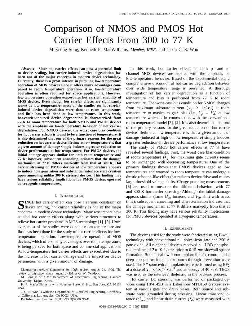
272 IEEE TRANSACTIONS ON ELECTRON DEVICES, VOL. 44, NO. 2, FEBRUARY 1997
TABLE I77 K (TOP) AND ROOM TEMPERATURE (BOTTOM) HOT-CARRIER STRESSEDDEVICE PARAMETERS.
ALL THE MEASUREMENTS PERFORMED AT ROOM TEMPERATURE FORCOMPARISON PURPOSE
gate and substrate current as a function of gate bias at roomtemperature and 77 K, respectively, with V. PMOShot carrier degradation at room temperature and 77 Kunder maximum gate ( ), maximum substrate current( ), and ( ) bias conditions are shownin Figs. 5(b) and 6(b), respectively. Threshold voltage ()is defined for a fixed current level in a given device (e.g.,
A m at mV). This power law relationshipof Fig. 5(b) at room temperature has been observed by otherresearchers [11] and is attributed to the logarithmic growthof filled traps from the drain toward the source junction[12]. The degradation is worst under stressing, whichis consistent with the work done by T.-C. Onget al. [13].Similar behavior has been observed for PMOS devices stressedat 77 K even though the degradation rate is much fasterat 77 K (Fig. 6). Unlike NMOS, ( ) stresscondition causes negligible hot carrier damage in PMOS atboth room temperature and 77 K.
Even though the initial degradation behavior of PMOSseems independent of temperature, subsequent annealing in-dicates that the damage mechanism at 77 K differs markedlyfrom that at 300 K. Fig. 7(a) and (b) shows the behavior of
and versus gate voltage for a given PMOS devicebefore hot carrier stressing (fresh), immediately after hotcarrier stressing at 77 K, and after an elevated temperatureanneal (95 C, 24 h and 120 C, 24 h). For subsequentcomparison purposes, all electrical measurements were per-formed at 300 K. The 6-m/1- m PMOSFET was hot carrierstressed at a drain bias of 7 V for 1600 s at 77 K.The gate potential was biased for maximum gate currentwhich occurred at V. After hot carrier testing and
characterization at 77 K, the device was left unbiased, warmedto temperature, and then followed by 300 K characterization.Note that immediately after hot carrier stressing at 77 K, thepositive voltage shift in and increase in follow thecharacteristic room temperature behavior. However, after thetwo high-temperature anneals, the and the voltage at thepeak rebound negatively (1 V) well beyond their initialvalues, and the peak is reduced over its post stress value.The same degree of rebound and degradation shown in Fig. 7has been observed after hot carrier stressing at 77 K withextensive room temperature anneals.
As shown in Fig. 8(a) and (b), we also performed room tem-perature hot carrier stressing followed by similar anneals andcharacterization. Despite a higher temperature initial anneal,and increased anneal duration, no similar hot-carrier-inducedrebound in and reduction in occurred. Measurementsconsistently indicate that only a moderate amount of recovery( still positive) is observed with 300 K stressing andanneal. A slight rebound and small degradation havebeen found with PMOS room temperature hot carrier stressingby others [14]; however, very high gate potentials of 13 Vand extended high-temperature anneals (80C) were required.Even so, only small changes were observed (50 mV of )with room temperature stressing compared to our rebound ofover 1 V for much more moderate stressing at 77 K.
To further investigate the differences between 77 K stressingand 300 K stressing with annealing, subthreshold slope andcharge pumping measurements were taken. The device stressedat 77 K shows a worsening (increased) subthreshold slopeafter subsequent annealing, while the device stressed at 300 Kshows an improved (decreased) subthreshold slope (Table I).
SONG et al.: COMPARISON OF NMOS AND PMOS HOT CARRIER EFFECTS 273
(a)
(b)
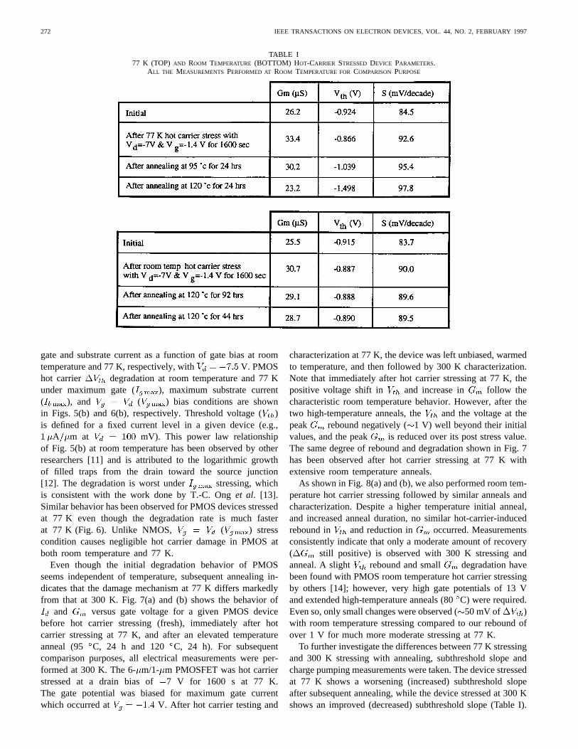
Fig. 9. Charge pumping measurements as a function of time and after hot carrier stress (a) at 77 K and (b) 300 K. Elevated temperature unbiasedanneals of Table I were performed at day 6 and day 11, respectively for the two stress conditions. All charge pumping measurements were performedat room temperature for comparison.
Also, as shown in Fig. 9, the room temperature stressed deviceshows an immediate, albeit small, increase in charge pumpingcurrent ( ) while the 77 K stressed device shows virtually noincrease in until after the elevated temperature anneal. Inaddition, the final maximum of is much larger for the 77 Kstressed device. Finally, there is a larger initial positive shiftin the value of the charge pumping characteristic forthe 300 K stressed device relative to the 77 K stressed device
( refers to the applied DC gate voltage about which thetriangular charge pumping wave varies). Using the relation [6]
(1)
274 IEEE TRANSACTIONS ON ELECTRON DEVICES, VOL. 44, NO. 2, FEBRUARY 1997
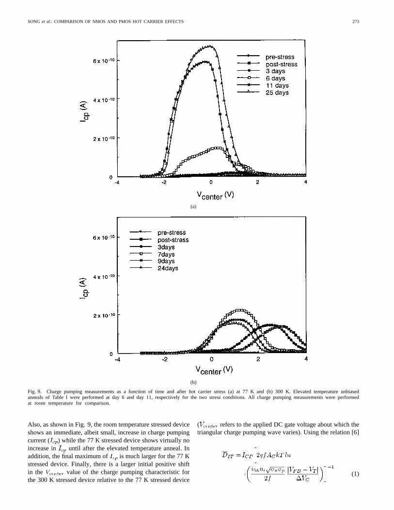
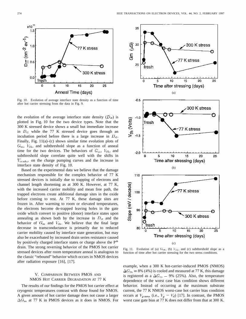
Fig. 10. Evolution of average interface state density as a function of timeafter hot carrier stressing from the data in Fig. 9.
the evolution of the average interface state density () isplotted in Fig. 10 for the two device types. Note that the300 K stressed device shows a small but immediate increasein while the 77 K stressed device goes through anincubation period before there is a large increase in.Finally, Fig. 11(a)–(c) shows similar time evolution plots of
, , and subthreshold slope as a function of annealtime for the two devices. The behaviors of , , andsubthreshold slope correlate quite well with the shifts in
on the charge pumping curves and the increase ininterface state density of Fig. 10.
Based on the experimental data we believe that the damagemechanism responsible for the complex behavior of 77 Kstressed devices is initially due to trapping of electrons andchannel length shortening as at 300 K. However, at 77 K,with the increased carrier mobility and mean free path, thetrapped electrons create additional damage sites in the oxidebefore coming to rest. At 77 K, these damage sites arefrozen in. After warming to room or elevated temperatures,the electrons become de-trapped leaving holes in the gateoxide which convert to positive (donor) interface states uponannealing as shown both by the increase in and thebehavior of and . We believe that the final largedecrease in transconductance is primarily due to reducedcarrier mobility caused by interface state generation, but mayalso be exacerbated by increased drain series resistance causedby positively charged interface states or charge above the Pdrain. The strong reversing behavior of the PMOS hot carrierstressed devices after room temperature anneal is analogous tothe classic “rebound” behavior which occurs in NMOS devicesafter radiation exposure [16], [17].
V. COMPARISON BETWEEN PMOS AND
NMOS HOT CARRIER DEGRADATION AT 77 K
The results of our findings for the PMOS hot carrier effect atcryogenic temperatures contrast with those found for NMOS.A given amount of hot carrier damage does not cause a larger
at 77 K in PMOS devices as it does in NMOS. For
(a)
(b)
(c)
Fig. 11. Evolution of (a)Gm, (b) Vth, and (c) subthreshold slope as afunction of time after hot carrier stressing for the two stress conditions.
example, when a 300 K hot-carrier-induced PMOS (NMOS)8% (4%) is cooled and measured at 77 K, this damage
is registered as a 9% (25%). Also, the temperaturedependence of the worst case bias condition shows differentbehavior. Instead of occurring at the maximum substratecurrent, the 77 K NMOS worst-case hot carrier bias conditionoccurs at (i.e., ) [17]. In contrast, the PMOSworst case gate bias at 77 K does not differ from that at 300 K.
SONG et al.: COMPARISON OF NMOS AND PMOS HOT CARRIER EFFECTS 275
However, the lack of change in worst-case hot carrier bias at77 K for PMOS devices does not appear to be in conflictwith the change in the NMOS worst-case bias condition. Foreach device type, the worst case 77 K bias conditions occurat the maximum gate current within the given bias range:
for NMOS and for PMOS. Even thoughthe origin of the gate current is different for each device type,electrons comprise the gate current [18] and hot carrier damageis worst at maximum gate current at low temperature for bothdevice types. At low temperature, electron trapping becomesthe dominant damaging mechanism and the electron trappingis closely related to the gate current. Therefore, gate currentappears to be the best metric for both P and NMOS hot carrierdegradation at 77 K.
VI. SUMMARY
For n-channel devices, the worst case bias condition forhot carrier effects is found to be a function of operatingtemperature. There exists a cross-over temperature, at whichthe worst bias condition changes from to . Theactivation energy, and thus the dominant damaging mechanismshows a clear transition near 200 K. One of the primaryfindings in this work is that the greatly reduced NMOS hotcarrier device lifetime at low temperature is simply due to thefact that a given amount of damage always induces a greaterreduction on device performance at low temperature.
For p-channel devices, hot carrier lifetime is much worseat low temperature, which is similar to n-channel devices.However, the worst case bias condition ( condition)does not change with temperature as with NMOS devices.A variety of hot carrier stresses, measurements, and annealshave shown that the PMOS hot carrier damage created at77 K is distinctly different from that created at 300 K.There is a strong rebound-like behavior of 77 K stressedPMOS devices with room temperature anneal which canresult in large threshold voltage shifts and markedly reduceddevice drive. The obvious pragmatic concern of this PMOSrebound-like effect is that the creation of latent damage at lowtemperature will suddenly reveal itself after warming to roomtemperature.
Based upon these findings and the results of NMOS hotcarrier stressing at 77 K, we believe that gate current may bethe best metric to employ for hot carrier modeling of bothdevice types at low temperatures.
ACKNOWLEDGMENT
The authors would like to thank G. Yabiku, S. Brown, C.Chang, and R. Hinojos for sample preparation and some ofthe device testing.
REFERENCES
[1] F.-C. Hsu and K.-Y. Chiu, “Evaluation of LDD MOSFET’s basedon hot-electron-induced degradation,”IEEE Electron Device Lett.,vol.EDL-5, p. 162, 1984.
[2] B. Doyle, M. Bourcerie, J.-C. Maretaux, and A. Boudou, “Interface statecreation and charge trapping in the medium-to-high gate voltage range(Vd=2 � Vg � Vd) during hot carrier stressing of n-MOS transistors,”IEEE Trans. Electron Devicesvol. 37, p. 744, 1990.
[3] C. Hu, S. C. Tam, F. C. Hsu, P. K. Ko, T. Y. Chan, and K. W.Terrill, “Hot-electron-induced MOSFET degradation-model, monitor,and improvement,”IEEE Trans. Electron Devices,vol. ED-32, p. 375,1985.
[4] E. Takeda and N. Suzuki, “An empirical model for device degradationdue to hot carrier injection,”IEEE Electron Device Lett.,vol. EDL-4,p. 111, 1983.
[5] K. K. Ng and G. W. Taylor, “Effects of hot carrier trapping in n-andp-channel MOSFET’s,”IEEE Trans. Electron Devices,vol. ED-30, p.871, 1983.
[6] G. Groeseneken, H. E. Maes, N. Beltran, and R. F. De Keersmaecker, “Areliable approach to charge-pumping measurements in MOS transistors,”IEEE Trans. Electron Devices,vol. ED-31, p. 42, 1984.
[7] P. Heremans, G. van den Bosch, R. Bellen, G. Groseneken, and H. E.Maes, “Understanding of the temperature dependence of channel hotcarrier degradation in the range 77 K to 300 K,” inTech. Dig.: Int.Electron Devices Meet.,1989, p. 67.
[8] M. Song, K. P. MacWilliams, J. Wang, J. C. S. Woo, and C. R.Viswanathan, “Temperature effects of hot-carrier-induced damage onNMOS device parameters and input referred noise,”IEEE ElectronDevice Lett.,submitted for publication.
[9] K. K. Ng and G. W. Taylor, “Effects of hot carrier trapping in n-andp-channel MOSFET’s,”IEEE Trans. Electron Devices,vol. ED-30, p.871, 1983.
[10] M. Koyanagi, A. G. Lewis, R. A. Martin, T.-Y. Huang, and J. Y. Chen,“Hot-electron-induced punchthrough (HEIP) effect in submicrometerPMOSFET’s,” IEEE Trans. Electron Devices,vol. ED-34, p. 839,1987.
[11] M. Brox, E. Wohlrab, and W. Weber, “A physical lifetime predictionmethod for hot carrier stressed P-MOS transistors,” inTech. Dig.: Int.Electron Devices Meet.,1991, p. 525.
[12] Q. Wang, M. Brox, W. H. Krautschneider, and W. Weber, “Explana-tion and model for the logarithmic time dependence of p-MOSFETdegradation,”IEEE Electron Device Lett.,vol. 12, p. 218, 1991.
[13] T.-C. Ong, K. Seki, P. K. Ko, and C. Hu, “P-MOSFET gate currentand device degradation,” inProc. Int. Reliab. Phys. Symp.,1989, p.178.
[14] Y. Pan, “The hot-carrier-induced degradation mechanisms of 0.8-�mLDD P-MOSFET with 850�C wet gate oxidation,” inProc. Int. Reliab.Phys. Symp.,1993, p. 43.
[15] P. S. Winokur and W. E. Boesch, Jr., “Annealing of MOS capacitorswith implications for test procedures to determine radiation hardness,”IEEE Trans. Nucl. Sci.,vol. NS-28, p. 4088, 1981.
[16] A. H. Johnson, “Super recovery of total dose damage in MOS devices,”IEEE Trans. Nucl. Sci.,vol. NS-31, p. 1427, 1984.
[17] M. Song, J. S. Cable, K. P. MacWilliams, and J. S. Woo, “Dependenceof LDD device optimization on stressing parameters at 77 K,” inTech.Dig.: Int. Electron Devices Meet.,1990, p. 223.
[18] I. Kato, H. Oka, S. Hijiya, and T. Nakamura, “1.5-�m gate CMOSoperated at 77 K,” inTech. Dig.: Int. Electron Devices Meet.,1984, p.601.
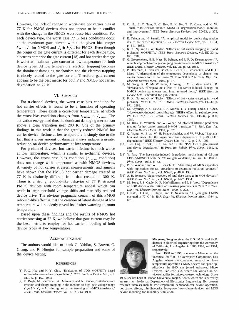
Miryeong Song received the B.S., M.S., and Ph.D.degrees in electrical engineering from the Universityof California, Los Angeles, in 1988, 1991, and 1994,respectively.
From 1988 to 1995, she was a Member of theTechnical Staff at The Aerospace Corporation, LosAngeles, where she conducted research on low-temperature operation CMOS devices for space ap-plications. In 1995, she joined Advanced MicroDevices, San Jose, CA, where she worked on de-vice reliability for microprocessor technology. Since
1996, she has been at Hannan University, Taejon, Korea, where she is currentlyan Assistant Professor, Department of Electronics Engineering. Her presentresearch interests include low-temperature semiconductor device operation,hot carrier effects, thin dielectrics, low-power/low-voltage devices, and MOSdevice modeling for reliability simulation.
276 IEEE TRANSACTIONS ON ELECTRON DEVICES, VOL. 44, NO. 2, FEBRUARY 1997
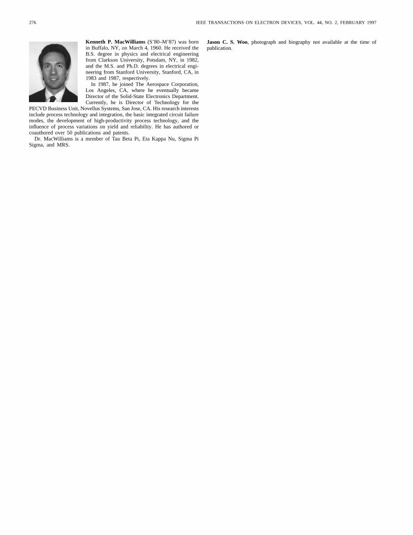
Kenneth P. MacWilliams (S’80–M’87) was bornin Buffalo, NY, on March 4, 1960. He received theB.S. degree in physics and electrical engineeringfrom Clarkson University, Potsdam, NY, in 1982,and the M.S. and Ph.D. degrees in electrical engi-neering from Stanford University, Stanford, CA, in1983 and 1987, respectively.
In 1987, he joined The Aerospace Corporation,Los Angeles, CA, where he eventually becameDirector of the Solid-State Electronics Department.Currently, he is Director of Technology for the
PECVD Business Unit, Novellus Systems, San Jose, CA. His research interestsinclude process technology and integration, the basic integrated circuit failuremodes, the development of high-productivity process technology, and theinfluence of process variations on yield and reliability. He has authored orcoauthored over 50 publications and patents.
Dr. MacWilliams is a member of Tau Beta Pi, Eta Kappa Nu, Sigma PiSigma, and MRS.
Jason C. S. Woo, photograph and biography not available at the time ofpublication.