1.2) operation of mos,pmos,nmos transistors
TRANSCRIPT

UNIT - 11.1) Introduction to VLSI Technology:
1.2) operation of MOS,PMOS,NMOS transistors


1.3) Fabrication of CMOS inverterBasic CMOS Technology
In early days of technology, the control gate of the MOS transistor was made withaluminum instead of polycrystalline silicon. It was difficult to align the metal over thechannel precisely; an offset in one direction or other would create a non-functioning ofthe transistor. To overcome these problems, the poly-silicon gate was introduced. Thispolysilicon would be deposited before source/drain diffusion. During the diffusion,source and drain regions are self-aligned with respect to the gate. This self-alignmentstructure reduces the device size. In addition, it eliminates the large overlap capacitancebetween gate and drain, while maintaining a continuous inversion layer between sourceand drain. In the case of metal gate process, Al deposition has to be carried out almost atthe end of fabrication because further high temperature processing would melt Al. In caseof self-aligned poly silicon gate technology, these restrictions are also circumvented.
Basic n-well CMOS processIn a standard n-well process, one of the first things made is the n-well in a p typesubstrate. Once the n-well is created, the active areas can be defined. The MOSFET isbuild within this active area. A very thin layer of silicon dioxide is grown on the surface.This will be used to insulate the gate from the surface. The thin layer of SiO2 is grownand covered with Si3N4. This will act as a mask during the subsequent channel stopimplant and field oxide growth. The channel stop implant is to prevent conductionbetween unrelated transistor source/drains. A thick additional layer oxide grows in bothdirections vertically where Si3N4 is absent. Layer of silicon dioxide under the polysilicongate (which will be created later) is known as gate oxide and that is not directly under thegate of a transistor is known as field oxide. The field oxide provides isolation betweentransistors. A threshold adjustment implant would be the next process step. This is carriedout to balance off the threshold voltage differences. The P-MOS results in a higher

©
threshold voltage level than nMOS with normal doping concentrations. With additionalnegative charges buried inside the channel, VT for pMOS could be controlled.
(a)
(b)Formation of n-well
Gate oxide covered with silicon nitride in the active areas
Polysilicon deposition is carried out and gate definition is then completed using the maskshown in fig (c). Note that the connection between two gate inputs in a CMOS inverter isachieved using the poly silicon. The source and drain diffusions for pMOS is carried outusing p-type diffusion. Boron is the most popular element used for this step. Similarly,source and drain diffusions for nMOS is carried out using n-type diffusion. Phosphorousand Arsenic can both be used for this step. Additional oxide is created, and then thecontact holes are cut in the oxide down to the diffusions and polysilicon. These contactscan be filled by metal permitted to flow into the holes. The drains of pMOS and nMOStransistors are connected by a metal line in order to take the output from the CMOSinverter.

(f)
Top view of Poly silicon mask
(d)
Poly silicon gate definition is completed
(e)
Transistor source/drain diffusion is completed
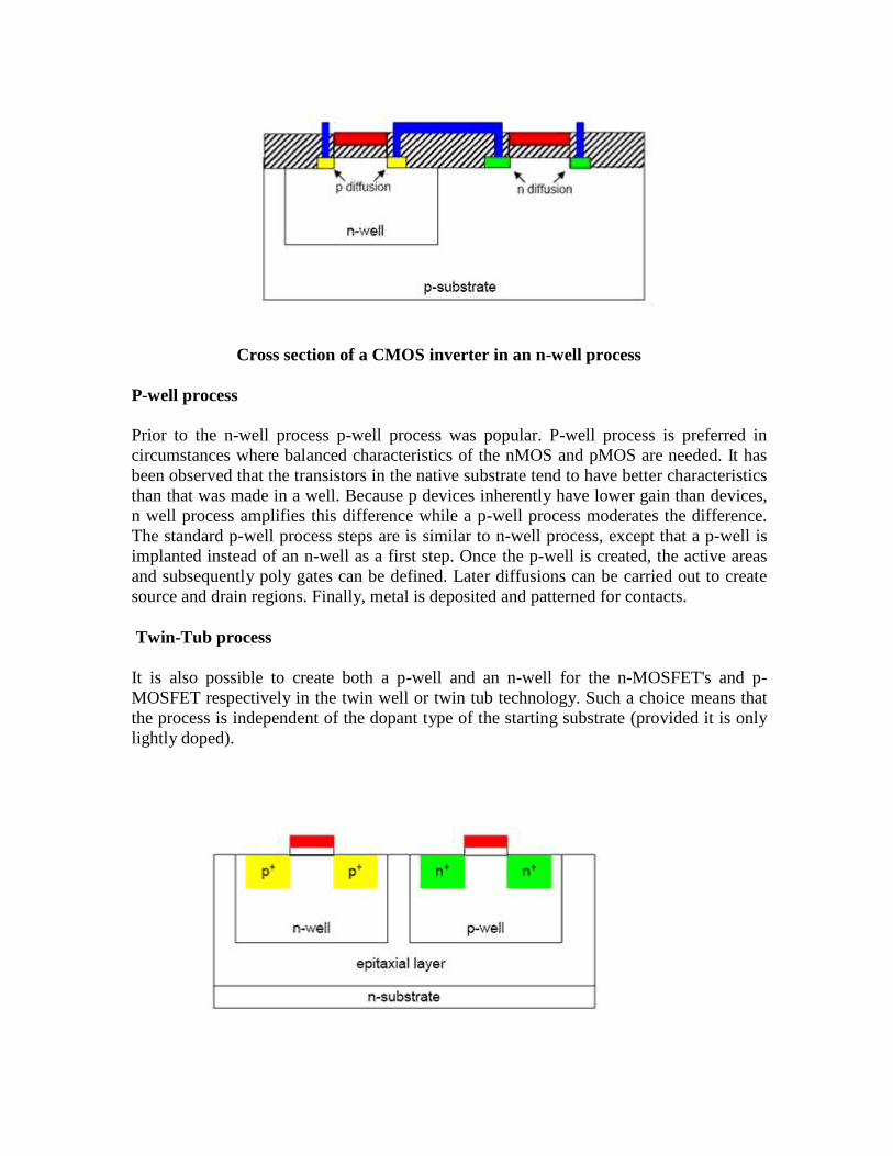
Cross section of a CMOS inverter in an n-well process
P-well process
Prior to the n-well process p-well process was popular. P-well process is preferred incircumstances where balanced characteristics of the nMOS and pMOS are needed. It hasbeen observed that the transistors in the native substrate tend to have better characteristicsthan that was made in a well. Because p devices inherently have lower gain than devices,n well process amplifies this difference while a p-well process moderates the difference.The standard p-well process steps are is similar to n-well process, except that a p-well isimplanted instead of an n-well as a first step. Once the p-well is created, the active areasand subsequently poly gates can be defined. Later diffusions can be carried out to createsource and drain regions. Finally, metal is deposited and patterned for contacts.
Twin-Tub process
It is also possible to create both a p-well and an n-well for the n-MOSFET's and p-MOSFET respectively in the twin well or twin tub technology. Such a choice means thatthe process is independent of the dopant type of the starting substrate (provided it is onlylightly doped).

A simplified sketch of twin-well CMOS process cross section


In lithography for micromachining, the photosensitive material used is typically aphotoresist (also called resist, other photosensitive polymers are also used). When resistis exposed to a radiation source of a specific a wavelength, the chemical resistance of theresist to developer solution changes. If the resist is placed in a developer solution afterselective exposure to a light source, it will etch away one of the two regions (exposed orunexposed). If the exposed material is etched away by the developer and the unexposedregion is resilient, the material is considered to be a positive resist (shown in figure 2a). Ifthe exposed material is resilient to the developer and the unexposed region is etchedaway, it is considered to be a negative resist (shown in figure 2b).

Figure 2: a) Pattern definition in positive resist, b) Pattern definition in negative resist

UNIT-2
Basic Electrical properties of MOS transistors


(b)Enhancement mode device:

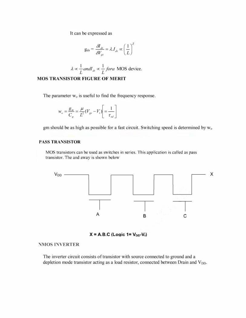

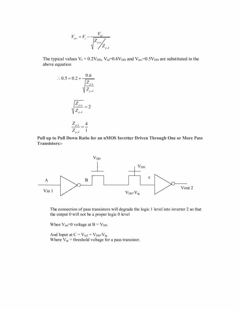
NMOS inverter
vout

NMOS inverter transfer characterstic