comparison of 4t and 6t finfet sram cells for subthreshold ... · with the spice approach, the...
TRANSCRIPT
IEEE TRANSACTIONS ON ELECTRON DEVICES, VOL. 58, NO. 3, MARCH 2011 609
Comparison of 4T and 6T FinFET SRAM Cells forSubthreshold Operation Considering Variability—A
Model-Based ApproachMing-Long Fan, Student Member, IEEE, Yu-Sheng Wu, Student Member, IEEE,
Vita Pi-Ho Hu, Student Member, IEEE, Chien-Yu Hsieh, Pin Su, Member, IEEE, and Ching-Te Chuang, Fellow, IEEE
Abstract—This paper investigates the cell stability of recentlyintroduced four-transistor (4T) and conventional six-transistor(6T) fin-shaped field-effect transistor static random access mem-ory (SRAM) cells operating in a subthreshold region using anefficient model-based approach to consider the impact of devicevariations. Compared with the 6T cell, this paper indicates that4T SRAM cells exhibit a better nominal READ static noise margin(RSNM) because of the reduced READ disturb. For 4T cells, thenearly ideal values of Vwrite,0 and Vwrite,1 guarantee the positivenominal WRITE static noise margin (WSNM) for selected cells.For half-selected cells on the selected bit line, a sufficient marginis observed between WRITE time (for selected cells) and WRITEdisturb (for half-selected cells). Using the established model-basedapproach, the variability of subthreshold 6T and 4T SRAM cellsis assessed with 1000 samples. Our results indicate that the 4Tdriverless cell with a larger μRSNM and a slightly worse σRSNMshows a comparable μ/σ ratio in RSNM with the 6T cell. Further-more, for a given cell area, 4T SRAM cells using relaxed devicedimensions with reduced σRSNM can outperform the 6T cell.For WRITE operation, 4T SRAM cells exhibit a superior WSNM,whereas the design margin between WRITE time and WRITE dis-turb needs to be carefully examined to ensure an adequate marginconsidering device variability.
Index Terms—Fin-shaped field-effect transistor (FinFET), staticnoise margin (SNM), subthreshold static random access memory(SRAM), variability.
I. INTRODUCTION
FOR ultralow-power applications in portable devices, im-planted medical instruments, and wireless body sensing
networks, operating circuits with the supply voltage Vdd belowthe threshold voltage VT has emerged as an effective solution toreduce power consumption [1]. However, the reduced Ion/Ioff
ratio and aggravated device variations in a subthreshold regimebecome serious concerns, particularly for static random accessmemory (SRAM) cells with minimum-size or sub-groundruledevices. The cell stability deteriorates with decreasing Vdd, and
Manuscript received June 30, 2010; revised October 16, 2010; acceptedNovember 21, 2010. Date of current version February 24, 2011. This work wassupported in part by the National Science Council of Taiwan under ContractNSC 99-2221-E-009-174, by the Ministry of Education in Taiwan under theAim for Top University Program, and by the Ministry of Economic Affairs inTaiwan under Contract 98-EC-17-A-01-S1-124. The review of this paper wasarranged by Editor S. Deleonibus.
The authors are with the Department of Electronics Engineering and theInstitute of Electronics, National Chiao Tung University, Hsinchu 300, Taiwan(e-mail: [email protected]).
Color versions of one or more of the figures in this paper are available onlineat http://ieeexplore.ieee.org.
Digital Object Identifier 10.1109/TED.2010.2096225
several novel bulk eight/ten-transistor cell structures have beenproposed to replace the conventional six-transistor (6T) SRAMcell for subthreshold applications [2]–[5].
Due to its superior gate control, a fin-shaped field-effecttransistor (FinFET) exhibits better subthreshold slope, reducedleakage current, and higher Ion/Ioff ratio. In addition, the useof a lightly-doped silicon fin improves the immunity to randomdopant fluctuation, making a FinFET a promising candidatefor emerging subthreshold SRAM applications [6], [7]. To as-sess and establish the feasibility of FinFET-based subthresholdSRAM cells, an extensive investigation considering the impactsof device variations on cell stability is required. Unlike bulkmetal–oxide–semiconductor field-effect transistor, the SPICEmodel for an extremely scaled FinFET device incorporatingcrucial quantum–mechanical effects is lacking. Therefore, tech-nology computer-aided design (TCAD) atomistic Monte Carlomixed-mode simulations considering various variation sourcesare often used to assess the statistical characteristics of SRAMcells [8]–[11]. However, limitations on the computational ef-ficiency, storage capacity, and sample size have hindered thefeasibility of quick assessment for SRAM cell design.
In this paper, a model-based approach is developed and em-ployed to efficiently investigate the impacts of device variationson the cell stability of four-transistor (4T)/6T subthresholdFinFET SRAM cells. The model is physically derived from thefundamental equations without fitting parameters. Comparedwith the SPICE approach, the model shows superior scalabilityand predictability. The remainder of this paper is organized asfollows: Section II describes the framework of our model-basedapproach used in this study. With the established methodol-ogy, two recently introduced 4T FinFET SRAM cells and theconventional 6T FinFET cell are compared in Section III. Theadvantages of 4T FinFET SRAM cells are demonstrated usingour model-based approach considering the impact of fin line-edge roughness (fin LER) on the cell stability. Finally, we drawthe conclusion in Section IV.
II. FRAMEWORK OF THE MODEL-BASED APPROACH
A. Atomistic TCAD Monte Carlo Simulation
To capture the atomic-level imperfections of each microscop-ically different device, sophisticated TCAD simulations [12]are needed. The discreteness of ionized dopant, ragged lineedge, and interface have been known to cause a mismatch in
0018-9383/$26.00 © 2011 IEEE
610 IEEE TRANSACTIONS ON ELECTRON DEVICES, VOL. 58, NO. 3, MARCH 2011
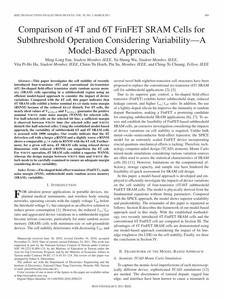
Fig. 1. Id–Vg characteristics of FinFET device considering fin LER. (Inset)Example of the FinFET samples with fin LER simulated in this work.
neighboring devices [13]. Among various local random varia-tion sources, LER-induced variation on the fin width (fin LER)of FinFET devices is the dominant variation source [8]. Hence,fin LER is considered in this paper to evaluate the robustness ofFinFET cell stability.
To simulate LER, rough line-edge patterns are generated bythe Fourier synthesis approach [14] with a correlation length of20 nm and a root-mean-square amplitude of 1.5 nm [8]. Atom-istic TCAD Monte Carlo simulations with 200 samples are thenperformed. Fig. 1 shows the Id–Vg subthreshold characteristicsof FinFET suffering from fin LER, and the inset illustrates oneof the simulated FinFET samples with fin LER.
B. Model Library Buildup
The analytical FinFET subthreshold drain-current model de-rived in [15] and [16] is used to bridge the gap between atom-istic TCAD and circuit-level simulations in this model-basedapproach. The proposed FinFET subthreshold drain-currentmodel has been shown to be capable of accurately describ-ing subthreshold drain-current characteristics for tied- andindependent-gate modes of operation [6]. In the subthresholdregion, the device Id–Vg characteristic can be described by thesubthreshold swing (S.S.) and the OFF-state current Ioff . Hence,the characteristic of each device with an irregular fin patterncan be captured by a set of effective fin width Wfin and gatework function (WF), which result in the same S.S. and Ioff
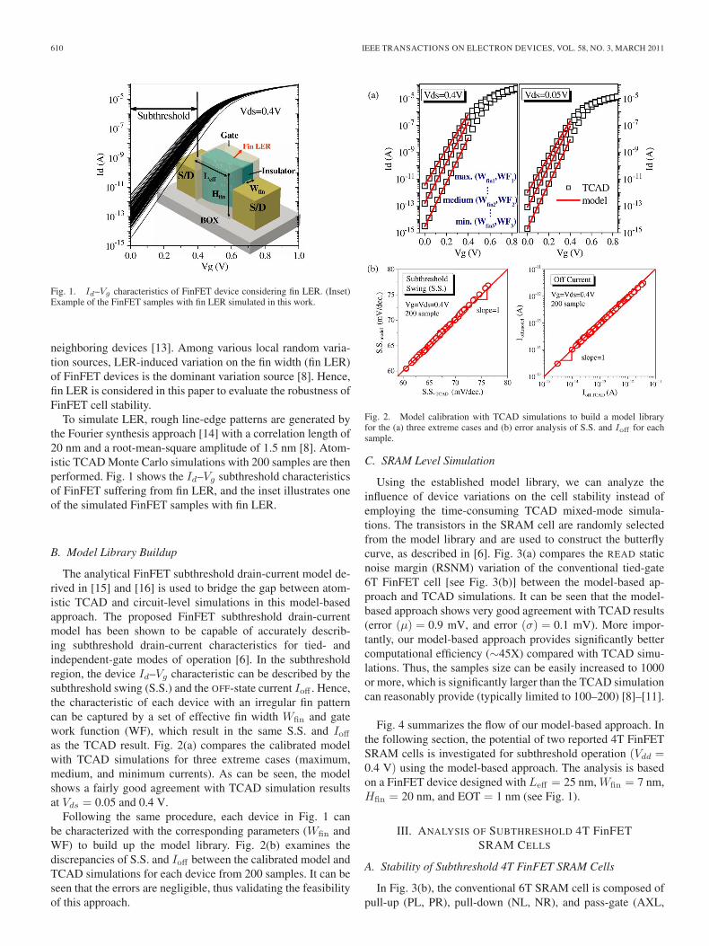
as the TCAD result. Fig. 2(a) compares the calibrated modelwith TCAD simulations for three extreme cases (maximum,medium, and minimum currents). As can be seen, the modelshows a fairly good agreement with TCAD simulation resultsat Vds = 0.05 and 0.4 V.
Following the same procedure, each device in Fig. 1 canbe characterized with the corresponding parameters (Wfin andWF) to build up the model library. Fig. 2(b) examines thediscrepancies of S.S. and Ioff between the calibrated model andTCAD simulations for each device from 200 samples. It can beseen that the errors are negligible, thus validating the feasibilityof this approach.
Fig. 2. Model calibration with TCAD simulations to build a model libraryfor the (a) three extreme cases and (b) error analysis of S.S. and Ioff for eachsample.
C. SRAM Level Simulation
Using the established model library, we can analyze theinfluence of device variations on the cell stability instead ofemploying the time-consuming TCAD mixed-mode simula-tions. The transistors in the SRAM cell are randomly selectedfrom the model library and are used to construct the butterflycurve, as described in [6]. Fig. 3(a) compares the READ staticnoise margin (RSNM) variation of the conventional tied-gate6T FinFET cell [see Fig. 3(b)] between the model-based ap-proach and TCAD simulations. It can be seen that the model-based approach shows very good agreement with TCAD results(error (μ) = 0.9 mV, and error (σ) = 0.1 mV). More impor-tantly, our model-based approach provides significantly bettercomputational efficiency (∼45X) compared with TCAD simu-lations. Thus, the samples size can be easily increased to 1000or more, which is significantly larger than the TCAD simulationcan reasonably provide (typically limited to 100–200) [8]–[11].
Fig. 4 summarizes the flow of our model-based approach. Inthe following section, the potential of two reported 4T FinFETSRAM cells is investigated for subthreshold operation (Vdd =0.4 V) using the model-based approach. The analysis is basedon a FinFET device designed with Leff = 25 nm, Wfin = 7 nm,Hfin = 20 nm, and EOT = 1 nm (see Fig. 1).
III. ANALYSIS OF SUBTHRESHOLD 4T FinFETSRAM CELLS
A. Stability of Subthreshold 4T FinFET SRAM Cells
In Fig. 3(b), the conventional 6T SRAM cell is composed ofpull-up (PL, PR), pull-down (NL, NR), and pass-gate (AXL,

FAN et al.: COMPARISON OF 4T AND 6T FINFET SRAM CELLS: MODEL-BASED APPROACH 611
Fig. 3. (a) Comparison of the RSNM variation between TCAD mixed-modesimulations and the model-based approach. (b) Schematic of the conventionaltied-gate 6T FinFET SRAM cell.
Fig. 4. Flow of the model-based approach to consider the impacts of devicevariations.
AXR) transistors. Pull-up and pull-down transistors form thecross-coupled inverter latch to store the data, and the cellis accessed by pass-gate devices. Due to the capability ofindependent-gate control, a single FinFET device has been pro-posed to replace the function of two traditional transistors [17]to reduce the transistor count and the circuit area. Similarly, theconventional 6T SRAM cell can also be reduced to 4T cells.Fig. 5 illustrates two types of recently introduced 4T FinFETSRAM cells reported in the literature [18].
The 4T loadless (LL) cell, as shown in Fig. 5(a), combinesthe function of the p-channel FET (PFET) pass-gate devicewith a PFET pull-up transistor using one single independent-gate controlled transistor (PL, PR). Notice that the source nodesof PL/PR are connected to the bit-line BL/BLB, which areprecharged to “High” (Vdd). The cell is activated when theword line (WL) goes to “Low.” Fig. 6(a) shows the READ
butterfly curve of 4T LL cell. As can be seen, the READ
disturb voltage Vread,0 of the 4T LL cell is negligibly smallas it is determined by the voltage divider effect betweenthe single-gate (SG)-mode pass-transistor PFET (one gate of
Fig. 5. Novel 4T SRAM cells using independent-gate control technique. (a)4T LL cell. (b) 4T DL cell [18].
Fig. 6. Comparison of butterfly curves for 4T LL cell with conventional 6TSRAM cell. (a) RSNM. (b) WSNM.
PL/PR) and the double-gate (DG)-mode pull-down n-channelFET (NFET) (tied-gate NL/NR). In addition, owing to thefully-conducting back gates (serving as pass-gate devices), thestrength of the front-gate devices of PL/PR (serving as pull-up devices) is enhanced, thus increasing the trip voltage ofthe cell. Compared with the conventional 6T cell, the 4T LLcell exhibits a better nominal RSNM. During WRITE operation,the virtual supply node VDL/VDR connecting to the low-going bit-line is pulled down to GND by the WRITE driver,thus facilitating the pull-down of the cell storage node. Assuch, Vwrite,0 becomes very low, resulting in a significantlylarger/better WSNM than that in the conventional 6T cell[see Fig. 6(b)].
In Fig. 5(b), the 4T driverless (DL) cell uses the back gatesof the pull-down transistors (NL, NR) as pass-gate transistors.
612 IEEE TRANSACTIONS ON ELECTRON DEVICES, VOL. 58, NO. 3, MARCH 2011
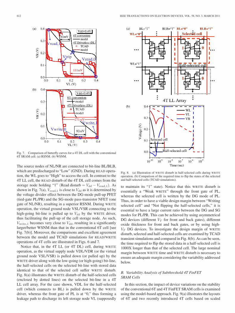
Fig. 7. Comparison of butterfly curves for a 4T DL cell with the conventional6T SRAM cell. (a) RSNM. (b) WSNM.
The source nodes of NL/NR are connected to bit-line BL/BLB,which are predischarged to “Low” (GND). During READ opera-tion, the WL goes to “High” to access the cell. In contrast to the4T LL cell, the READ disturb of the 4T DL cell comes from thestorage node holding “1” (Read disturb = Vdd − Vread,1). Asshown in Fig. 7(a), Vread,1 is close to Vdd as it is determined bythe voltage divider effect between the DG-mode pull-up PFET(tied-gate PL/PR) and the SG-mode pass-transistor NFET (onegate of NL/NR), resulting in a superior RSNM. During WRITE
operation, the virtual ground node VSL/VSR connecting to thehigh-going bit-line is pulled up to Vdd by the WRITE driver,thus facilitating the pull-up of the cell storage node. As such,Vwrite,1 becomes very close to Vdd, resulting in a significantlylarger/better WSNM than that in the conventional 6T cell [seeFig. 7(b)]. Moreover, the comparisons and excellent agreementbetween the model and TCAD simulations for READ/WRITE
operations of 4T cells are illustrated in Figs. 6 and 7.Notice that, in the 4T LL (or 4T DL) cell, during WRITE
operation, as the virtual supply node VDL/VDR (or the virtualground node VSL/VSR) is pulled down (or pulled up) by theWRITE driver along with the low-going (or high-going) bit-line,the half-selected cells on the selected bit-line with stored dataidentical to that of the selected cell suffer WRITE disturb.Fig. 8(a) illustrates the WRITE disturb of the half-selected cells(enclosed by dotted lines) on the selected bit-line in a 4TLL cell array. For the case shown, VDL for the half-selectedcell (which connects to BL) is pulled down by the WRITE
driver, whereas the front gate of PL is at “0,” thus forming aleakage path to discharge its left storage node VL (supposedly
Fig. 8. (a) Illustration of WRITE disturb in half-selected cells during WRITE
operation. (b) Comparison of the required time to flip the states of the selectedand half-selected cells (TCAD simulations).
to maintain its “1” state). Notice that this WRITE disturb isessentially a “Weak WRITE” through the front gate of PL,whereas the selected cell is written by the DG mode of PL.Thus, in order to have a viable design margin between “Writingselected cell” and “Not flipping the half-selected cells,” it isessential to have a large current ratio between the DG and SGmodes for PL/PR. This can be achieved by using asymmetricalDG devices (different VT for front and back gates), differentoxide thickness for front and back gates, or by using high-VT DG devices. To investigate the design margin of WRITE
disturb, selected and half-selected cells are examined by TCADtransient simulations and compared in Fig. 8(b). As can be seen,the time required to flip the stored data in a half-selected cell is1000X longer than that of the selected cell. The large nominalmargin between WRITE time and WRITE disturb is necessary toensure an adequate margin considering the variability addressedbelow.
B. Variability Analysis of Subthreshold 4T FinFETSRAM Cells
In this section, the impact of device variations on the stabilityof the conventional 6T and 4T FinFET SRAM cells is examinedusing the model-based approach. Fig. 9(a) illustrates the layoutsof 6T and two recently introduced 4T cells based on scaled

FAN et al.: COMPARISON OF 4T AND 6T FINFET SRAM CELLS: MODEL-BASED APPROACH 613
Fig. 9. (a) FinFET cell layouts for the conventional 6T, 4T LL, and 4TDL cells with identical device sizes. (b) and (c) RSNM/HSNM variabilitycomparisons of the cells [see (a)] with the same device sizes (Leff = 25 nmand Wfin = 7 nm).
design rules from the published 32-nm technologies [19] andthe scaling factor from the International Technology Roadmapfor Semiconductors roadmap. Compared with the 6T cell, the4T cells show 25% area reduction.
Fig. 9(b) illustrates the RSNM variability of the cells with1000 samples for the same device sizes. Owing to the worseelectrostatic integrity of independent-gate operation, 4T SRAMcells show broader dispersion, thus larger σRSNM. If we targetthe value of the μ/σ ratio to be 5–6 for robust cell design, thecalculated μ/σ ratio of the 4T DL cell, with a larger/better nom-inal RSNM and a slightly larger/worse σRSNM, is comparableto the 6T cell and meets the requirement. The hold static noisemargin (HSNM) variations are also assessed [see Fig. 9(c)] forvarious cells. It can be seen that HSNM, with a larger μHSNM,is better, as expected in general.
If the cells are compared based on the same cell area (chipdensity), 4T SRAM cells with fewer transistors have the flex-ibility of relaxing device size and the potential of reducing
Fig. 10. (a) FinFET cell layouts for the conventional 6T, 4T LL, and 4T DLcells with identical cell areas. (b) and (c) RSNM/HSNM variability compar-isons with the same cell area (4T cells with Leff = 32 nm and Wfin = 10 nm).
variations. Fig. 10(a) illustrates the layouts for 6T and relaxed4T SRAM cells with comparable cell areas. The transistorsize in 4T SRAM cells can be loosened from (Leff ,Wfin) =(25 nm, 7 nm) to (32 nm, 10 nm) with identical subthresholdslopes. In Fig. 10(b) and (c), the variability of RSNM/HSNMfor 6T and relaxed 4T SRAM cells is examined. As expected,the relaxed 4T cells exhibit a tighter distribution due to lessvariation sensitivity in the larger device. In addition, the calcu-lated μ/σ ratios of RSNM/HSNM increase and outperform the6T cell.
In Fig. 11(a)–(c), the WSNM variations are analyzed for the6T and reported 4T SRAM cells. For selected cells, the lowvalue of Vwrite,0 and the high value of Vwrite,1 for 4T LL andDL cells guarantee successful WRITE. 4T SRAM cells exhibita better WSNM than that for the conventional 6T cell [seeFig. 11(a)]. However, the WRITE disturb in the half-selectedcells on the selected bit-line may become a concern with device

614 IEEE TRANSACTIONS ON ELECTRON DEVICES, VOL. 58, NO. 3, MARCH 2011
Fig. 11. Direct-current transfer characteristics of (a) conventional 6T, (b) 4TLL, and (c) DL cells during WRITE with identical device sizes. (d) Transientanalysis of Write time and WRITE disturb for 4T LL and DL cells (TCADsimulations with 150 samples).
variations. Fig. 11(d) examines the WRITE time and WRITE
disturb of 4T SRAM cells using TCAD transient Monte Carlosimulations. As expected, the margin between WRITE timeand WRITE disturb decreases under the influence of devicevariations for 4T LL and DL cells. It can also be seen that the 4TLL cell exhibits a larger margin (about one order of magnitude
Fig. 12. Stored states in the worst-case half-selected cells with various WLpulsewidths for 4T (a) LL and (b) DL cells. (Inset) Timing diagrams.
difference between WRITE time and WRITE disturb) than the 4TDL cell.
Based on the analysis in Fig. 11(d), the WL pulse-widthshould be carefully controlled within the margin to maintainthe data storing in the half-selected cells. In Fig. 12, the worstcase (the tail of the distribution) of the half-selected cells fromFig. 11 is investigated. Fig. 12(a) and (b) illustrates the storedstates in the worst-case half-selected cells and the correspond-ing timing diagrams with various WL pulse-widths for 4TLL and DL cells, respectively. As can be seen in the timingdiagrams, in the 4T LL (or DL) cell, the WL goes to “Low”(or “High”) to activate the selected row and execute WRITE
operation. During the WL “ON” period, the stored states inthe half-selected cells suffer WRITE disturb. The activated WLpulse-width should be properly designed to avoid the flippingof the stored states in the half-selected cells. In Fig. 12, thevoltages in the stored nodes (VL/VR) of the worst-case half-selected cell at the tail of distribution are shown versus theWL pulse-width. It is found that the data stored in the worst-case half-selected cell are maintained if the WL pulse is chosenproperly.
IV. CONCLUSION
We have employed an efficient model-based approach to con-sider the impact of device variations on the FinFET SRAM cellstability. Specifically, the stability of two recently introduced4T FinFET SRAM cells has been investigated and comparedwith the conventional 6T cell in the subthreshold region. Owingto the reduced READ disturb, 4T SRAM cells exhibit a bet-ter nominal RSNM than the conventional 6T cell. Moreover,

FAN et al.: COMPARISON OF 4T AND 6T FINFET SRAM CELLS: MODEL-BASED APPROACH 615
the nearly ideal values of Vwrite,0 and Vwrite,1 guarantee thepositive WSNM for selected 4T LL and DL cells. For half-selected cells on the selected bit-line, the margin betweenWRITE time and WRITE disturb has been assessed by TCADsimulations. The variability of the 4T and conventional 6T cellshas also been assessed using the model-based approach with1000 samples for each case. Our results indicate that the 4TDL cell with a larger μRSNM and a slightly worse σRSNMshows a comparable μ/σ ratio in RSNM with the conventional6T cell. Furthermore, for a given cell area, 4T cells with fewertransistors have the flexibility of using relaxed device design.Thus, σRSNM can be reduced, and the μ/σ ratios in RSNMfor 4T cells can outperform the conventional 6T cell. ForWRITE operation, 4T SRAM cells show a superior WSNM forselected cells, whereas the margin between WRITE time(for selected cells) and WRITE disturb (for half-selected cellson selected bit-line) needs to be carefully examined to ensurean adequate margin under variability.
ACKNOWLEDGMENT
The authors would like to thank the National Center forHigh-Performance Computing in Taiwan for the use of com-putational facilities and software.
REFERENCES
[1] A. Wang, B. H. Calhoun, and A. P. Chandraksan, Sub-Threshold Designfor Ultra Low-Power Systems. New York: Springer-Verlag, 2006.
[2] T.-H. Kim, J. Liu, J. Keane, and C. H. Kim, “A high-density subthresholdSRAM with data-independent bitline leakage and virtual-ground replicascheme,” in Proc. ISSCC Tech. Dig., 2007, pp. 330–331.
[3] I. J. Chang, J.-J. Kim, S. P. Park, and K. Roy, “A 32 Kb 10T subthresholdSRAM array with bit-interleaving and differential read scheme in 90 nmCMOS,” in Proc. ISSCC Tech. Dig., 2008, pp. 388–389.
[4] J. P. Kulkarni, K. Kim, and K. Roy, “A 160 mV robust Schmitt triggerbased subthreshold SRAM,” IEEE J. Solid-State Circuits, vol. 42, no. 10,pp. 2303–2313, Oct. 2007.
[5] J. P. Kulkarni, K. Kim, S. P. Park, and K. Roy, “Process variation tolerantSRAM array for ultra low voltage applications,” in Proc. Des. Autom.Conf., 2008, pp. 108–113.
[6] M.-L. Fan, Y.-S. Wu, V. P.-H. Hu, P. Su, and C.-T. Chuang, “Investigationof cell stability and write ability of FinFET subthreshold SRAM usinganalytical SNM model,” IEEE Trans. Electron Devices, vol. 57, no. 6,pp. 1375–1381, Jun. 2010.
[7] J. Kim and K. Roy, “Double gate-MOSFET subthreshold circuit for ul-tralow power applications,” IEEE Trans. Electron Devices, vol. 51, no. 9,pp. 1468–1474, Sep. 2004.
[8] E. Baravelli, A. Dixit, R. Rooyackers, M. Jurczak, N. Speciale, andK. De Meyer, “Impact of line-edge roughness on FinFET matching per-formance,” IEEE Trans. Electron Devices, vol. 54, no. 9, pp. 2466–2474,Sep. 2007.
[9] K. Samsudin, B. Cheng, A. R. Brown, S. Roy, and A. Asenov, “Integrat-ing intrinsic parameter fluctuation description into BSIMSOI to forecastsub-15 nm UTB SOI based 6T SRAM operation,” Solid State Electron.,vol. 52, no. 1, pp. 86–93, Jan. 2006.
[10] E. Baravelli, L. De Marchi, and N. Speciale, “ VDD scalability of FinFETSRAMs: Robustness of different design options against LER-inducedvariations,” Solid State Electron., vol. 54, no. 9, pp. 909–918, Sep. 2010.
[11] C. Shin, M. H. Cho, Y. Tsukamoto, B.-Y. Nguyen, C. Mazure, B. Nikolic,and T.-J. K. Liu, “Performance and area scaling benefits of FD-SOI tech-nology for 6-T SRAM cells at the 22-nm node,” IEEE Trans. ElectronDevices, vol. 57, no. 6, pp. 1301–1309, Jun. 2010.
[12] Sentaurus TCAD, C2009-06 Manual, Sentaurus Device, 2009.[13] A. Asenov, A. R. Brown, J. H. Davies, S. Kaya, and G. Slavcheva,
“Simulation of intrinsic parameter fluctuations in decananometer andnanometer-scale MOSFETs,” IEEE Trans. Electron Devices, vol. 50,no. 9, pp. 1837–1852, Sep. 2003.
[14] A. Asenov, S. Kaya, and A. R. Brown, “Intrinsic parameter fluctuations indecananometer MOSFETs introduced by gate line edge roughness,” IEEETrans. Electron Devices, vol. 50, no. 5, pp. 1254–1260, May 2003.
[15] Y.-S. Wu and P. Su, “Sensitivity of multigate MOSFETs to processvariations—An assessment based on analytical solutions of 3-D Poisson’sequation,” IEEE Trans. Nanotechnol., vol. 7, no. 3, pp. 299–304,May 2008.
[16] Y.-S. Wu and P. Su, “Sensitivity of gate-all-around nanowire MOSFETsto process variations—A comparison with multigate MOSFETs,” IEEETrans. Electron Devices, vol. 55, no. 11, pp. 3042–3047, Nov. 2008.
[17] M.-H. Chiang, K. Kim, C.-T. Chuang, and C. Tretz, “High-densityreduced-stack logic circuit techniques using independent-gate controlleddouble-gate devices,” IEEE Trans. Electron Devices, vol. 53, no. 9,pp. 2370–2377, Sep. 2006.
[18] B. Giraud, A. Vladimirescu, and A. Amara, “A comparative study of 6Tand 4T SRAM cells in double-gate CMOS with statistical variation,” inProc. Int. Conf. Circuits Syst., 2007, pp. 3022–3025.
[19] X. Chen, S. Samavedam, V. Narayanan, K. Stein, C. Hobbs, C. Baiocco,W. Li, D. Jaeger, M. Zaleski, H. S. Yang, N. Kim, Y. Lee, D. Zhang,L. Kang, J. Chen, H. Zhuang, A. Sheikh, J. Wallner, M. Aquilino,J. Han, Z. Jin, J. Li, G. Massey, S. Kalpat, R. Jha, N. Moumen, R. Mo,S. Kirshnan, X. Wang, M. Chudzik, M. Chowdhury, D. Nair, C. Reddy,Y. W. Teh, C. Kothandaraman, D. Coolbaugh, S. Pandey, D. Tekleab,A. Thean, A. Thean, M. Sherony, C. Lage, J. Sudijono, R. Lindsay,J. H. Ku, M. Khare, and A. Steegen, “A cost effective 32 nm high-K/metal gate CMOS technology for low power applications with single-metal/gate-first process,” in VLSI Symp. Tech. Dig., 2008, pp. 88–89.
Ming-Long Fan (S’09) was born in Taichung,Taiwan, in 1983. He received the B.S. and theM.S. degrees from National Chiao Tung University,Hsinchu, Taiwan, in 2006 and 2008, respectively.He is currently working toward the Ph.D. degreein the Institute of Electronics, National Chiao TungUniversity.
His current research interests include the designand modeling of subthreshold static random accessmemory in scaled/exploratory technologies.
Yu-Sheng Wu (S’09) was born in Tainan, Taiwan,in 1982. He received the B.S. and M.S. degrees inelectronics engineering from National Chiao TungUniversity, Hsinchu, Taiwan, in 2004 and 2006,respectively. He is currently working toward thePh.D. degree in the Institute of Electronics, NationalChiao Tung University.
His current research interests include designand modeling of advanced complementarymetal–oxide–semiconductor devices.

616 IEEE TRANSACTIONS ON ELECTRON DEVICES, VOL. 58, NO. 3, MARCH 2011
Vita Pi-Ho Hu (S’09) was born in Changhua,Taiwan, in 1982. She received the B.S. degreefrom National Chiao Tung University, Hsinchu,Taiwan, in 2004. She is currently working toward thePh.D. degree in the Institute of Electronics, NationalChiao Tung University.
Her research interests include analysis and designof ultralow-power static random access memories innanoscaled technologies.
Chien-Yu Hsieh was born in Hsinchu, Taiwan, in1985. He received the B.S. degree from NationalChung Hsing University, Taichung, Taiwan, in 2008and the M.S. degree from National Chiao Tung Uni-versity, Hsinchu, in 2010.
Pin Su (S’98–M’02) received the B.S. and M.S. de-grees in electronics engineering from National ChiaoTung University, Hsinchu, Taiwan, and the Ph.D.degree from the Department of Electrical Engineer-ing and Computer Sciences, University of California,Berkeley.
From 1997 to 2003, he conducted his doctoral andpostdoctoral research in silicon-on-insulator (SOI)devices at Berkeley. He was also one of the majorcontributors to the unified BSIMSOI model, whichis the first industrial standard SOI metal–oxide–
semiconductor field-effect transistor model for circuit design. Since August2003, he has been with the Department of Electronics Engineering, NationalChiao Tung University, where he is currently an Associate Professor. He hasauthored or coauthored over 100 research papers in refereed journals andinternational conference proceedings. His research interests include silicon-based nanoelectronics, modeling and design for advanced complementary MOS(CMOS) devices, and device/circuit interaction and cooptimization in nano-CMOS.
Ching-Te Chuang (S’78–M’82–SM’91–F’94) re-ceived the B.S.E.E. degree from National TaiwanUniversity, Taipei, Taiwan, in 1975 and the Ph.D.degree in electrical engineering from the Universityof California, Berkeley, in 1982.
From 1977 to 1982 he was a Research Assistantwith the Electronics Research Laboratory, Univer-sity of California, Berkeley, working on bulk andsurface acoustic wave devices. He joined the IBMT. J. Watson Research Center, Yorktown Heights,NY, in 1982. From 1982 to 1986, he worked on
scaled bipolar devices, technology, and circuits. He studied the scaling proper-ties of epitaxial Schottky barrier diodes, did pioneering works on the perimetereffects of advanced double-poly self-aligned bipolar transistors, and designedthe first subnanosecond 5-kb bipolar emitter-coupled logic static random accessmemory (SRAM). From 1986 to 1988, he was the Manager of the Bipolar VeryLarge Scale Integration (VLSI) Design Group, working on low-power bipolarcircuits, high-speed high-density bipolar SRAMs, multigigabyte/second fiber-optic data-link circuits, and scaling issues for bipolar/bipolar complementarymetal–oxide–semiconductor devices and circuits. Since 1988, he has managedthe High-Performance Circuit Group, investigating high-performance logicand memory circuits. Since 1993, his group has been primarily responsiblefor the circuit design of IBM’s high-performance CMOS microprocessorsfor enterprise servers, PowerPC workstations, and game/media processors.Since 1996, he has been leading the efforts in evaluating and exploringscaled/emerging technologies, such as partially depleted/silicon on insulator(SOI), ultrathin body/SOI, strained-Si devices, hybrid orientation technology,and multigate/fin-shaped field-effect transistor devices, for high-performancelogic and SRAM applications. Since 1998, he has been responsible for theResearch VLSI Technology Circuit Codesign strategy and execution. His grouphas also been very active and visible in leakage/variation/degradation tolerantcircuit and SRAM design techniques. He took early retirement from IBM to joinNational Chiao Tung University, Hsinchu, Taiwan, as a Chair Professor with theDepartment of Electronics Engineering in February 2008. He has authored orcoauthored over 290 papers. He is the holder of 31 U.S. patents and has 14 thatare still pending.
Dr. Chuang served on the Device Technology Program Committee for theInternational Electron Devices Meeting in 1986 and 1987 and on the ProgramCommittee for Symposium on VLSI Circuits from 1992 to 2006. He wasthe Publication/Publicity Chairman for Symposium on VLSI Technology andSymposium on VLSI Circuits in 1993 and 1994, and the Best Student PaperAward Subcommittee Chairman for Symposium on VLSI Circuits from 2004to 2006. He was elected an IEEE Fellow in 1994 “For contributions to high-performance bipolar devices, circuits, and technology.” He has received oneOutstanding Technical Achievement Award, one Research Division Outstand-ing Contribution Award, five Research Division Awards, and twelve InventionAchievement Awards from IBM. He was the corecipient of the Best PaperAward at the 2000 IEEE International SOI Conference. He has received theOutstanding Scholar Award from Taiwan’s Foundation for the Advancementof Outstanding Scholarship for 2008–2013. He has authored many invitedpapers in international journals such as the International Journal of High-Speed Electronics, PROCEEDINGS OF IEEE, IEEE Circuits and DevicesMagazine, and the Microelectronics Journal. He has presented numerousplenary, invited, or tutorial papers/talks at international conferences such asthe International SOI Conference; Design Automation Conference (DAC);VLSI-Technology, System, and Application; International Solid-State CircuitsConference Microprocessor Design Workshop; VLSI Circuit Symposium ShortCourse; International Symposium on Quality Electronic Design; InternationalConference on Computer-Aided Design; Asia-Pacific Microwave Conference,VLSI-Design, Automation, and Test; International Symposium on Circuitsand Systems; Memory Technology, Design, and Testing; World Scientificand Engineering Academy and Society; VLSI Design/CAD Symposium; andInternational Variability Characterization Workshop.