comparative analysis of 32 bit carry look ahead adder...
TRANSCRIPT

International Journal of Science, Engineering and Technology Research (IJSETR), Volume 3, Issue 10, October 2014
ISSN: 2278 – 7798 All Rights Reserved © 2014 IJSETR 2768
COMPARATIVE ANALYSIS OF 32 BIT CARRY LOOK
AHEAD ADDER USING
HIGH SPEED CONSTANT DELAY LOGIC
V.Reethika Rao(1)
, Dr.K.Ragini(2)
PG Scholar, Dept of ECE, G. Narayanamma Institute of Technology and Science, Hyderabad, India. (1)
Assistant Professor, Dept of ECE, G. Narayanamma Institute of Technology and Science, Hyderabad, India. (2)
Abstract:
In this paper, high speed constant delay logic is
implemented for32 bit carry look ahead adder.
The objective of CD logic is to reduce power
dissipation and mainly speed in the critical path of
carry generation (longest path from first to last
carry output). The 32 bit CLA is implemented
with other logics and the results are tabulated and
compared. From the implementation results, the
low power and high speed CD logic shows better
power reduction and less delay by 40% than other
method. The PDP is therefore better than the
existing method. Simulation is done using H spice
2008.03 soft ware and the delay is checked using
CosmoScope z 2007.03 software.
1.0 INTRODUCTION
The main challenging areas in VLSI are performance,
cost, testing, area, reliability and power. The demand
for portable computing devices and communication
system are increasing rapidly. These applications
require low power dissipation. The main aim of these
devices is to generate low power with high fault
coverage. Generally power dissipation of a system in
test mode is more than in normal mode. The ability to
design, fabricate and test Application Specific
Integrated Circuits (ASICs) as well as FPGAs with
gate count of the order of a few tens of millions has
led to the development of complex embedded SOC.
Testing of integrated circuits is important to
ensure high level of quality in products. The Built-In-
Self-Test (BIST) is one of most popular test solutions
to test the embedded cores. Test pattern generation is
vital in any BIST circuit. Since off-chip
communication between the FPGA and a processor is
bound to be slower than on chip communication, in
order to minimize the time required for adjustment of
the parameters, the built in self test approach is
proposed for this method.
Analysis of power for testing:
Various sources of power dissipation in CMOS are,
Static Power Dissipation
Dynamic power Dissipation
Static Power Dissipation:
It is the power dissipated when there is no
switching activity within the circuit. Ideally, CMOS
circuit dissipates no static power, since there is no
direct path from VDD to GND. But practically MOS
transistor never acts as perfect switch. There is
always leakage current which flows when the input(s)
to and the outputs of a gate are not changing, leads to
static power dissipation. It is the short circuit current
that flows when VDD is connected to VSS during
International Journal of Science, Engineering and Technology Research (IJSETR), Volume 3, Issue 10, October 2014
ISSN: 2278 – 7798 All Rights Reserved © 2014 IJSETR 2769
transition between high to low or low to high at any
node.
The static power dissipation is given by
P static = V DD* I leakage (1)
Ileakage= is (eqV/kT-1) (2)
Where Vdd is the supply voltage
is is reverse saturation current
V is diode voltage
K is Boltzmann’s constant (1.38Ψ 10-23 J/K)
Q is electronic charge (1.602Ψ 10-19 C)
T is temperature
Dynamic Power Dissipation:
It is due to switching transient current and
charging & discharging of load capacitance.
Transient power consumption is due to the current
that flows only when the transistors of the devices are
switching from one logic state to another. The
average power consumption of internal circuit node i
can be given by
Pi=0.5Vdd2C0FiSif (3)
Where f is the clock frequency
C0 is load capacitance
The product of Fi and Si is called the weighted
switching activity of internal circuit node i.
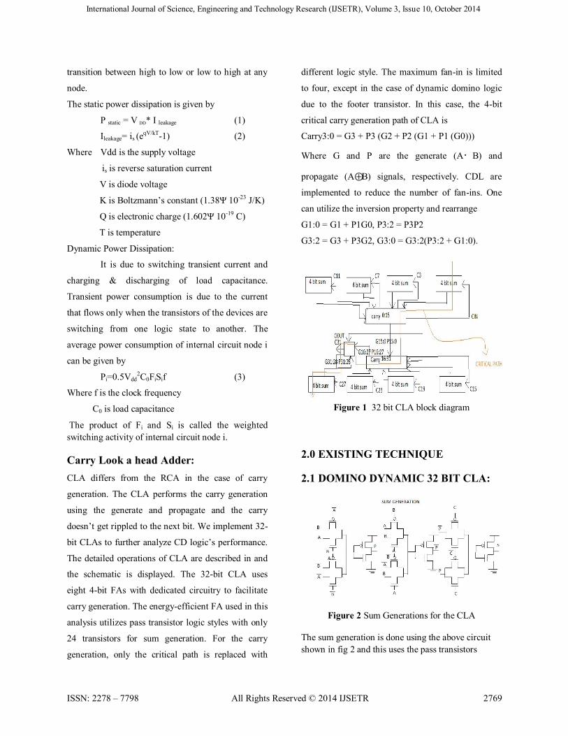
Carry Look a head Adder:
CLA differs from the RCA in the case of carry
generation. The CLA performs the carry generation
using the generate and propagate and the carry
doesn’t get rippled to the next bit. We implement 32-
bit CLAs to further analyze CD logic’s performance.
The detailed operations of CLA are described in and
the schematic is displayed. The 32-bit CLA uses
eight 4-bit FAs with dedicated circuitry to facilitate
carry generation. The energy-efficient FA used in this
analysis utilizes pass transistor logic styles with only
24 transistors for sum generation. For the carry
generation, only the critical path is replaced with
different logic style. The maximum fan-in is limited
to four, except in the case of dynamic domino logic
due to the footer transistor. In this case, the 4-bit
critical carry generation path of CLA is
Carry3:0 = G3 + P3 (G2 + P2 (G1 + P1 (G0)))
Where G and P are the generate (A・B) and
propagate (A⊕B) signals, respectively. CDL are
implemented to reduce the number of fan-ins. One
can utilize the inversion property and rearrange
G1:0 = G1 + P1G0, P3:2 = P3P2
G3:2 = G3 + P3G2, G3:0 = G3:2(P3:2 + G1:0).
Figure 1 32 bit CLA block diagram
2.0 EXISTING TECHNIQUE
2.1 DOMINO DYNAMIC 32 BIT CLA:
Figure 2 Sum Generations for the CLA
The sum generation is done using the above circuit
shown in fig 2 and this uses the pass transistors

International Journal of Science, Engineering and Technology Research (IJSETR), Volume 3, Issue 10, October 2014
ISSN: 2278 – 7798 All Rights Reserved © 2014 IJSETR 2770
Figure 3 4 bit Carry generations of Domino-dynamic
logic in 32 bit CLA
The fig 3 is for the carry generations in the domino-
dynamic logic. This logic carry isgenerated by the
generate ’G’ and propagate ’P’blocks.Where the
Propagate P= A XOR B
Generate G=A AND
The carry in is given to the first bit and the
carry to the next 4 bit block is generated by the above
circuit.The above circuit is implemented by the
equation given below
Carry3:0 = G3 + P3(G2 + P2(G1 + P1(G0))).

International Journal of Science, Engineering and Technology Research (IJSETR), Volume 3, Issue 10, October 2014
ISSN: 2278 – 7798 All Rights Reserved © 2014 IJSETR 2771
Figure 4. Output waveforms of domino dynamic 32
bit CLA.
The above fig 4 shows the output waveforms of the
32 bits of the outputs of every single 1 bit full adder
and each 4 bits are shown in separate window for the
clear view of the output waveforms and every sum
and carry out put are verified as full adder and the
frequency is trans wave up to 100nano seconds with
the supply voltage vdd=1.8v.
3. LATEST METHOD
Figure 5 CD logic carry circuit
Figure 6 CD logic sum circuit
3.1 CD Logic Operations
To mitigate the above-mentioned problems, CD logic
is proposed with a schematic shown in Fig. 7(a).
Timingblock(TB) creates an adjustable window
period to reduce the static power dissipation. Logic
Block (LB) helps to reduce the unwanted glitch and
also makes cascading CD logic feasible.A buffer
implemented in CD logic with schematics of TB and
LB is shown in fig 7(a) & (b).
When CLK is low, CD logic enters the
evaluation period and three scenarios can take place:
namely, the contention, C-Q delay, and D-Q delay
modes. The contention mode happens when CLK is
low while IN remains at logic "1." In this case, X is at
a nonzero voltage level which causes Out to
International Journal of Science, Engineering and Technology Research (IJSETR), Volume 3, Issue 10, October 2014
ISSN: 2278 – 7798 All Rights Reserved © 2014 IJSETR 2772
experience a temporary glitch. The duration of this
glitch is determined by the local window width,
which is determined by the delay between CLK and
CLK_d. When CLK_d becomes high, and if X
remains low, then Y rises to logic "1," and turns off
M1.Thus the contention period is over, and the
temporary glitch at Out is eliminated. C-Q delay
mode takes places when IN make a transition from
high to low before CLK becomes low. When CLK
becomes low, X rises to logic "1" and Y remains at
logic "0" for the entire evaluation cycle. The delay is
measured by the falling edge of both CLK and Out:
hence the name C-Q delay. D-Q delay mode utilizes
the pre-evaluated characteristic of CD logic to enable
high-performance operations. In this mode, CLK falls
from high to low before IN transit, hence X initially
rises to a nonzero voltage level. As soon as IN
become logic "0," while Y is still low, then X quickly
rises to logic "1.
Figure 7. (a) CD logic block diagram (b) buffer
4.0 RESULTS AND DISCUSSIONS
PROPOSED TECHNIQUE
CD 32 bit CLA:
Figure 8 Sum Generations for the CLA
The sum generation is done using the above circuit
shown in fig 8 and this uses the pass transistors
Figure 9 8 bit Carry generations of CD logic in 32
bit CLA
The fig 9 is for the carry generations in the CD logic.
This logic carry is generated by the generate ’G’ and
propagate ’P’blocks.
Where the Propagate P= A XOR B
Generate G=A AND B
The carry in is given to the first bit and the carry to
the next 4 bit block is generated by the above circuit.
The above circuit is implemented by the equation
given below
Carry3:0 = G3 + P3(G2 + P2(G1 + P1(G0)))

International Journal of Science, Engineering and Technology Research (IJSETR), Volume 3, Issue 10, October 2014
ISSN: 2278 – 7798 All Rights Reserved © 2014 IJSETR 2773
Figure 10 Simulated output waveforms of the CD
logic in 32 bit CLA
The outputs of the cla is presented above and with
each window showing the outputs of the 4 bits
each.the outputs are verified to be as that of a full
adder function and the outputs are plotted at the
voltage supply of vdd=1.8v of trans 100nsec.
The delay of the CD logic is thoroughly
enhanced and its speed increases and the power
consumption is also less.

International Journal of Science, Engineering and Technology Research (IJSETR), Volume 3, Issue 10, October 2014
ISSN: 2278 – 7798 All Rights Reserved © 2014 IJSETR 2774
Discussions on proposed CD logic:
Table 1 Simulation results of 32 bit CLA
Domino
dynamic
CD
logic
Avg
power(W)
2.03E-4 2E-4
Propagation
delay(sec)
176.67E-
12
105.45E-
12
Power
delay product
358.4E-
16
210.9E-16
The power of the pseudo dynamic logic is more as
the static power dissipation is present and the delay
of the pseudo is more compared to the other logics
and the delay of the CD logic style is less and power
consumption is less and the PDP of the CD logic is
best compared to domino dynamic logic.
5.0 CONCLUSIONS
CD logic is high performance logic style with the
self-reset circuitry. The timing block reduces the
contention and power consumption is reduced. The
delay is reduced in the critical path as the circuitry
has an advantage of pre-evaluation in the D-Q delay
mode and this reduces the delay.
In 32 bit CLA CD logic is 40.4% faster than domino
dynamic.PDP of 32 bit CLA is 41.4% and 59% of cd
logic. CD logic primarily concentrates on delay
improvement at the critical path and yields better
PDP.
REFERENCES
[1] Chuang.P, Li.D, and Sachdev.M, Design of a
64-bit low-energy high-performance adderusing
dynamic feedthroughlogic," in Circuits and Systems,
2009. ISCAS 2009.IEEE International Symposium
on, pp. 3038-3041, 2009.
[2] Ming-Bo Lin, “Introduction to VLSI Systems: A
Logic, Circuit, and System Perspective“, chapter
8,dynamiccircuits,pg no:401.
[3] Navarro-Botello.V, Montiel-Nelson.J.A, and
Nooshabadi.S, Low Power Arithmetic Circuit
inFeedthroughDyanmic CMOS Logic," 49th IEEE
International Midwest Symposium on Circuits and
Systems, vol. 1, pp. 709-712, 2006. 19, 22
[4]V.Navarro-Botello,Montiel
Nelson.J.A,andNooshabadi.S, Analysis of High-
Performance Fast FeedthroughLogic Families in
CMOS," Circuits and Systems II:Express Briefs,
IEEE Transactions on, vol. 54, no. 6, pp. 489-493,
2007.
[5] Nooshabadi.S and Montiel-Nelson.J.A, “Fast
feedthrough logic: A high-performance logic
family for GaAs,” IEEE Trans. Circuits Syst.I, Reg.
Papers, vol. 51, no. 11, pp. 2189–2203, Nov. 2004
[6] Zimmermann.R and Fichtner.W ,Low-power
logic styles : CMOS versus pass-transistor logic,
IEEE J.Solid-State Circuits vol.32,no.7, pp.1070-
1090, Jul.1997
[7] Friedman.VandLiu.S, \Dynamic logic
CMOS circuits," Solid-State Circuits, IEEE Journal
of,vol.19, pp. 263 -266, April 1984.