colourtelevision trainingmanual supplement …
TRANSCRIPT

COLOURTELEVISIONTRAININGMANUALSUPPLEMENT E2 —G CHASSIS
E3 —B CHASSIS
PIP(PICTURE IN PICTURE)ANDSVM(SCAN VELOCITYMODULATION)CIRCUIT ANALYSIS
A14800 WLY/89/l.000/SI REFERENCENO. WM-520058
SANYO ELECTRIC CO. .LTD.
JAPAN
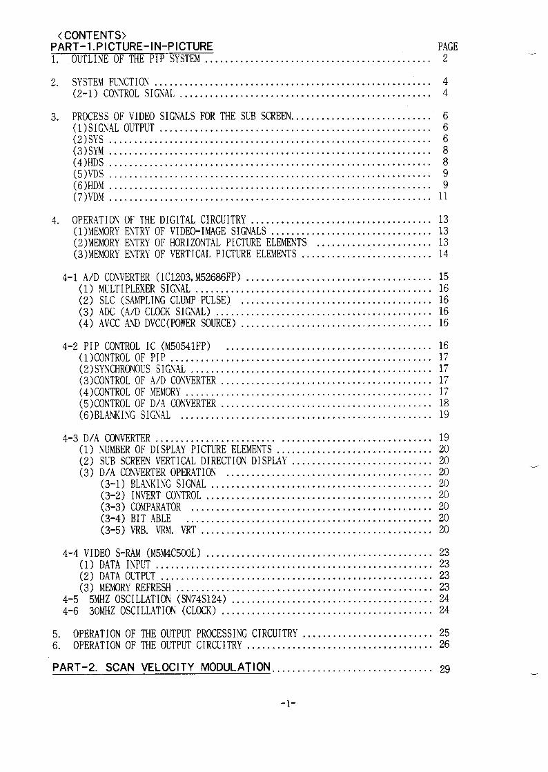
<CONTENTS>PART- l, PICTURE-IN-PICTURE1.
ATTm T Tim nv mm nrn r17rmm1
2.
3.
4,
uulLIIvE ur II-IDrir 3131 EIVI. . . . . . . . . . . . . . . . . . . . . . . . . . . . . . . . . . . . . . . . . . . . .
SYSTEMFUNCTION. . . . . . . . . . . . . . . . . . . . . . . . . . . . . . . . . . . . . . . . . . . . . . . . . . . . . . .(2-1) CONTROLSIGNAL. . . . . . . . . . . . . . . . . . . . . . . . . . . . . . . . . . . . . . . . . . . . . . . . . .
PROCESSOF VIDEOSIGNALSFORTHESUB SCREEN. . . . . . . . . . . . . . . . . . . . . . . . . . . .(l)SIGNAL OUTPUT. . . . . . . . . . . . . . . . . . . . . . . . . . . . . . . . . . . . . . . . . . . . . . . . . . . . . .(2)SYS . . . . . . . . . . . . . . . . . . . . . . . . . . . . . . . . . . . . . . . . . . . . . . . . . .(3) SYM::::::::::::::.. . . . . . . . . . . . . . . . . . . . . . . . . . . . . . . . . . . . . . . . . . . . . . . . .(4)HDS . . . . . . . . . . . . . . . . . . . . . . . . . . . . . . . . .,00 . . . . . . . . . .(5)vDs:::::::::: . . . . . . . . . . . . . . . . . . . . . . . . . . . . . . . . . . . . . . . . . . . . . . . . . . . . . .
. . . . . . . .
(6)HDM. . . . . . . . . . . . . . . . . . . ...0... . . . . . . . . . . . . . . . . . . . . . . . . . . . . . . . . . . . . . .(7)vDM . . . . . . . . . . . . . . . . . . . . . . . . . . . . . . . . . . . . . . . . . . . . . . . . . . . . . . . . . . . . . . . .
OPERATIONOF THEDIGITALCIRCUITRY. . . . . . . . . . . . . . . . . . . . . . . . . . . . . . . . . . . .(l) MEMOR~ENTRI’OF VIDEO-IMAGESIGNALS. . . . . . . , e. . . . . . . . , . . , , . . . . . . . . . .(2) MEMORY,ENTRYOF HORIZONTALPICTUREELEMENTS. . . . . . . .(3) MEMORIENTRYOF VERTICALPICTGREELEMENTS
. . . . . . . . . . . . . . .. . . . . . . . . . . . . . . . . . . . . . . . . .
4-1 A/DCONVERTER(IC1203, M52686FP)(1) MULTIPLEXERSIGNAL
. . . . . . . . . . . . . . . . . . . . . . . . . . . . . . . . . . . . .. . . . . . . . . . . . . . . . . . . . . . . . . . . . . . . . . . . . . . . . . . . . . . .
(2) SLC (SAMPLINGCLUMPPULSE) . . . . . . . . . . . . . . . . . . . . . . . . . . . . . . . . . . . . . .(3) ADC(A/DCLOCKSIGNAL). . . . . . . . . . . . . . . . . . . . . . . . . . . . . . . . . . . . . . . . . . .(4) AVCCANDDVCC(POWERSOURCE). . . . . . . . . . . . . . . . . . . . . . . . . . . . . . . . . . . . . .
4-2 PIP CONTROLIC (M50541FP) . . . . . . . . . . . . . . . . . . . . .(l)CONTROLoF Pip . . . . . . . . . . . . . : : : : : : : : : : : : : : : : : : . . . . . . . . . . . . . . . . . . . . .(2) SYNCHRONOWSIGNAL. . . . . . . . . . . . . . . . . . . . . . . . . . . . . . . . . . . . . . . . . . . . . . . .(3)coNTRoL oFA/DcoN\~ERTER. . . . . . . . . . . . . . . . . . . . . . . . . . . . . . . . . . . . . . . . . .(4)CONTROLOF MEMORY. . . . . . . . . . . . . . . . . . . . . . . . . . . . . . . . . . . . . . . . . . . . . . . . .(5)coNTRoL oFD/.AcoNwRTER . . . . . . . . . . . . . . . . . . . . . . . . . . . . . . . . . . . . . . . . . .(6) BLANKINGSIGNAL . . . . . . . . . . . . . . . . . . . . . . . . . . . . . . . . . . . . . . . . . . . . . . . . . .
4-3D/AcoNvERTER . . . . . . . . . . . . . . . . . . . . . . . . . . . .(1) WMBEROF DISPLAYPICTLREELEMENTS. . . .
. . . . . . . . . . . . . . . . . . . . . . . . . .
(2) SUB SCREENVERTICALDIRECTIONDISPLAY. . . . . . . . . . . . . . . . . . . . . . . . . . .
. . . . . . . . . . . . . . . . . . . . . . . . . . . .(3) D/ACOWERTEROPERATION. . . . . . . . . . . . . . . . . . . . . . . . . . . . . . . . . . . . . . . . .
(3-1)(3-2)(3-3)(3-4)(3-5)
BLi4VKINGSIGNAL. . . . . . . . . . . . . . . . . . . . . . . . . . . . . . . . . . . . . . . . . . . .INVERTCONTROL. . . . . . . . . . . . . . . . . . . . . . . . . . . . . . . . . . . . . . . . . . . . .COMPARATOR. . . . . . . . . . . . . . . . . . . . . . . . . . . . . . . . . . . . . . . . . . . . . . . .BIT .4BLE . . . . . . . . . . . . . . . . . . . . . . . . . . . . . . . . . . . . . . . . . . .VRB. WM. Vii::: . . . . . . . . ..0.... . . . . . . . . . . . . . . . . . . . . . . . . . . . .
4-4 VIDEOS-RAM(M5M4C500L). . . . . . . . . . . . . . . . . . . . . . . . . . . . . . . . . . . . . . . . . . . . .(l) DATAINPUT. . . . . . . . . . . . . . . . . . . . . . . . . . . . . . . . . . . . . . . . . . . . . . . . . . . . . . .(2) DATAOUTPUT. . . . . . . . . . . . . . . . . . . . . . . . . . . . . . . . . . . . . . . . . . . . . . . . . . . . . .(3) MEMORYREFRESH. . . . . . . . . . . . . . . . . . . . . . . . . . . . . . . . . . . . . . . . . . . . . . . . . . .
4-5 5MHZOSCILLATION(SN74S124) . . . . . . . . . . . . . . . . . . . . . . . . . . . . . . . . . . . . . . . .4-6 30MHZOSCILLATION(CLOCK). . . . . . . . . . . . . . . . . . . . . . . . . . . . . . . . . . . . . . . . . .
5. OPERATIONOF THEOUTPUTPRWESSINGCIRCUITRY. . . . . . . . . . . . . . . . . . . . . . . . . .6. OPERATIONOF THEOUTPUTCIRCLUTRY. . . . . . . . . . . . . . . . . . . . . . . . . . . . . . . . . . . . .
PART-2. SCAN VELOCITY Modulation . . . . . . . . . . . . . . . . . . . . . . . . . . . . . . . .
PAGE2
44
6668899
11
13131314
1516161616
16171’71’71’71819
192020202020202020
232323232424
2526
29
-1-
FOREWORDThis manual describes the SANYO PIP (Picture in picture) and SVM(scan velocity
modu Iat ion system) that have been introduced to the SANYO E2-G and E3-B chassis, for readersto understand the outline of them. In this manual, the process of the video signals andthe synchronous signals for PIP system are mainly explained. Those models that have adoptedthe systems are as follows; (At present in 1989)
E2-G chassis : CEP2149E3 chassis : CEP2559/2559S/2559TX
cEP3359T/3359Tx/3359 TxsCBP3359, CAP3359TX, CZP3359TX, CPP3359TX etc.Note: E2-G chassis has no SVM system.
1,OUTL INE OF THE PIP(PICTURE-IN-PI CTURE) SYSTEMFigure 1 shows a block diagram outline of the PIP system.
Fundamentally, the PIP system is a system that permits TV signal images now being receivedL (on a channel other than the channel to which the TV is set), or video image signals being
input from an external source, to be superimposed (the ‘ sub screen’ ) over one part of the TVscreen for display to the viewer. The video signals that are to be displayed on the subscreen are, first of all,R-Y and G-Y) signals atthe Y signals and the B-Yare converted to six-bitinscribed in the memory.
separated into luminance (Y) signals and color-d if ference (B-Y,the Y/C (luminance/chrominance) signal-processing circuitry. Afterand R-Y signals have each passed through the low-pass filter, theydigital data by the A/D (analog-to-digital) converter, and are
When the digital signals thus entered in the memory are taken out from the memory asa result of a command from the PIP controller (I C1201), those digital signals arereconverted to analog signals by the D/A (digital-to-analog) converter, but at this timethey are converted to Y, B-Y and R-Y signals in which the times for the horizontal andvertical dimensions of the screen (the sub screen, to be used for display of the reconvert-ed signals) are compressed to one-third. These analog signals are then input to the matrixcircuitry and are there converted to the individual RGB primary-color signals.
Signals (frame signals, to produce the frame of the sub screen) output from the PIPcontroller, and blanking signals (for superimposition of the sub screen onto the mainscreen), are both input to the matrix circuitry, where they are combined with the previously
L described reconverted primary-color signals, and these signals are then superimposed ontoone part of the TV screen. A block diagram of the PIP processing circuitry is shown inFigure 1,i
,
-2-

MA
INV
IDE
OIN
Q21
05Q
2106
Q21
07
IC21
01
1513
06S
P
Q21
02
–%=7
--m
PIP
bV
ideo
si@
for
PIP
IV
-SY
NC
~1Q
2131
4H
-SY
NC
rA/O Cof
w.
M52
666
FP
——
Q21
41Q
2142
Q21
UQ
2145
~
-nIC12
0ES
CK
LS
N74
S12
4*
5MH
2D
SC
Co
ntr
ol
Sip
ul
frc+
’11C
Pu
*L
-E
l-—
——
——
y—P
IPA
dre
saC
ON
TR
OL
ER
-1L
‘-:
~S
lc,s
ocM
5054
1W
M5M
4C50
0L6B
ITS
OA
TA
r‘r
-
6bit
sO
igit
dD
AT
A1
DA
Y
:mO
UT
PU
T+E
l-
F=5
?,Q
2163
Q21
62Q
2161
Q21
64Q
2160
cl-w
SIG
NA
L-Y
IC21
03
TA
7676
AP R-Y
B-Y
,—IQ
2162
}~
~D
AR
OA
B
VR
B,V
RM
,k71
T OJA ‘
,“-m
:
D/A
DIA
CO
NV
.C
ON
V,
CO
NV
.Y
R-Y
B-Y
M52
679~
M52
679F
PM
5267
9FP
IC12
06IC
1205
IC12
M
●-El
r’-
I1
FR
AM
ES
ION
AL
IIN
PU
TS
IGN
AL
SIP
ER
IWO
SE
Sl&
4AL
“11
I$—
—
wQ21
74IC
2106
SW
ITC
HA
N56
621C
2175
*
=
Q21
72
TE
xl:R
OB
-Y
-—r—
R-Y
I
BL
AN
XIN
OW
Y—
PIP
com
aS
IQN
AL
S=1
3=lF
UN
ll_U
E1G
7S
<F
ig.1
Blo
ckD
iagr
am>
(

Main Picture
IVIDEO SIGNAL
‘0’ MA’Np’’’”’+=~: ‘GB~W,’C~
BLANKING
MATRIXBLANKING
1-4 A ~
VIDEO SIGANLFOR PIP
e;= ~ ‘:: : ‘“E’
A/D CONVERTER
Fig,2 PIP SYSTEM BLOCK DIAGRAM
L
L
-4-

2. SYSTEM FUNCTIONSThe PIP controller (IC1201, M50541FP) can, as a result of control at the CPU (IC1701),
be used to perform the PIP functions described below.
2-1 CONTROL SIGNAL(1) PIP ON/OFF:
(2) LOCATE :
(3) FREEZE :
(4) SELECT :
The PIP ON/OFF signal functions to display or .----1 *L- mlm ------
display.The LOCATE signal moves the position (on thePIP screen display is presented.The FREEZE signal stops(’ freezes’ )the movingpresent a still-image display.The SELECT signal functions for selection of
GdIlL5i L[le rlr WJ WII
main screen) at which the
PIP screen display to
either TV broadcast signalsor external video signals as the signal source for the PIP screen display.
The control signals described above are controlled at the remote-control transmitter;signals that correspond to the various functions are emitted from the terminals of the CPU(ICI 701, MAB8461PW146) noted below in response to the act ivat ion of the various control keyson the remote-control transmitter.
~Pin No. lFunction ]Level lDescription I
25 STILL H: Still-image display IL: Ordinary-moving-image display
24 m : PIP ONON/OFF :: PIP OFF
23 LEF/RIG 22 23LL: PIP screen at upper left part of the main screen
22 fiP/BOT L H: PIP screen at lower left part of the main screenHL: PIP screen at upper right part of the main screenH H: PIP screen at lower right part of the main screen
21 SELECT H: TV broadcast signals are shown on PIP screen.L: Externally input video signals are shown on PIP screen.
<Table 1. IC1701 PIP control signal>
The SELECT function described above is performed as explained below.The selection is made whether to display, as the display images onTV broadcast signals (now being received by the TV set) or videoto the unit from an external source.The selection and switching to make possible either the TV broadcastreceived by the TV set)or video signals from an external source are made(IC1 391, LC4066B).The reason that each signal passes through two contacts with in the
the PIP screen, thesignals being input
signals (now beingby the switching IC
IC is in order tosufficiently maintain the degree of attenuation at the switch section (while OPEN), andto prevent the occurrence of signal leakage. External video signals follow the path 21-pinsocket (SKIRT input) to Q1381, IC1391(8) to IC1391(1 1); TV signals now being broadcastfollow the path IC101 (17), Q131, Q132, IC1391(4) to IC1391(1).The control-select signals from the CPU are input to IC1391 after passing through IC1701 pin(21), K17P(1), K21R(5), Q211O, K21Q (3), K13Q (3) and Q1391.
-5-
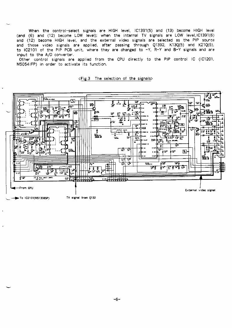
When the control-select signals(and (6) and (12) become LOW level);and (12) become HIGH level, and theand those video signals are applied,
are HIGH level, IC1391(5) and (13) become HIGH levelwhen the internal TV signals are LOW level, IC1391(6)external video signals are selected as the PIP sourceafter passing through Q1392, K13Q(5) and K210(5).
to IC2101 of the PIP PCB unit, where they are changed to -Y, R-Y and B-Y signals and’a~einput to the A/D converter.Other control signals are applied from the CPU directly to the PIP control IC (IC1201,
M50541FP) in order to activate its function.
<Fig.3 The selection of the signals>
fii-d-t
— I I *wi-- I
7L
m
#bak~’r l-1111 11 L II
!
k--From CPU IExtarnal vidao signal
- +To IC2101(M513O8SP) TV signal from Q132
-6-
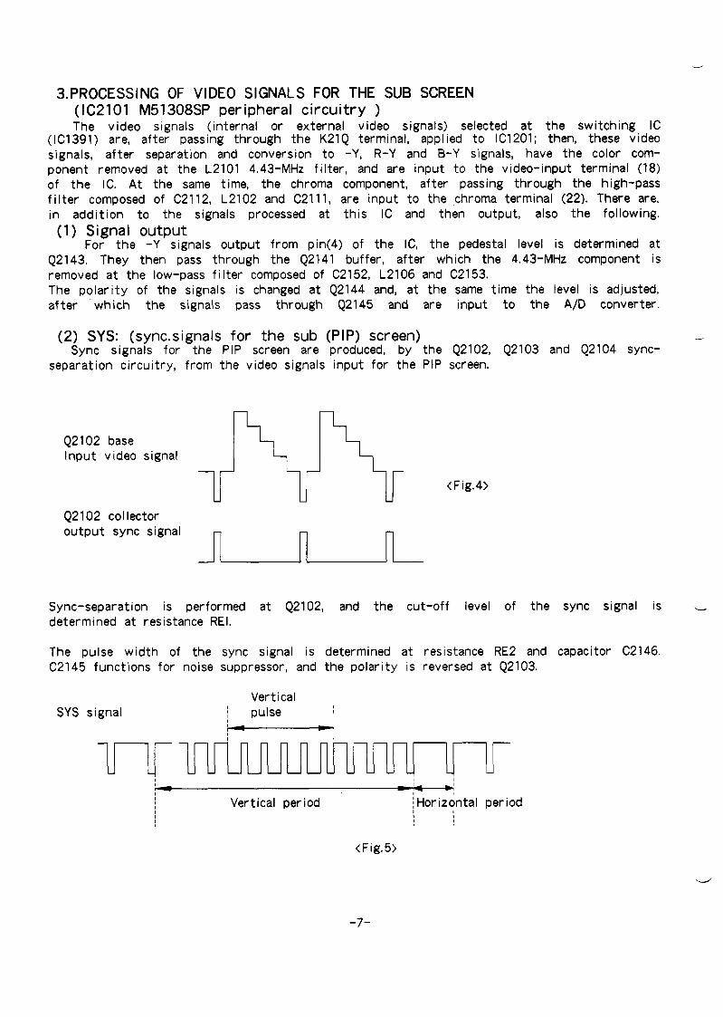
3. PROCESS ING OF VIDEO SIGNALS FOR THE SUB SCREEN(IC2101 M51308SP peripheral circuitry )The video signals (internal or external video signals) selected at the switching IC
(IC1391) are, after passing through the K21Q terminal, applied to IC1201; then, these videosignals, after separation and conversion to -Y, R-Y and B-Y signals, have the color com-ponent removed at the L2101 4.43-MHz filter, and are input to the video-input terminal (18)of the IC. At the same time, the chroma component, after passing through the high-passfilter composed of C2112, L2102 and C2111, are input to the chroma terminal (22). There are,in addition to the signals processed at this IC and then output, also the following.
(1) Signal outputFor the -Y signals output from pin(4) of the IC, the pedestal level is determined at
Q2143, They then pass through the Q2141 buffer, after which the 4.43-MHz component isremoved at the low-pass f i Iter composed of C2152, L2106 and C2153.The polarity of the signals is changed at Q2144 and, at the same time the level is adjusted,after which the signals pass through Q2145 and are input to the A/D converter,
(2) SYS: (sync. signals for the sub (PIP) screen)Sync signals for the PIP screen are produced, by the Q2102, Q2103 and Q2104 sync-
separation circuitry, from the video signals input for the PIP screen.
Q2102 baseInput video signal
Q2102 COIIectoroutput sync signal
<Fig.4)
n n nSync-separation is performed at Q2102, and the cut-off level of the sync signal is -determined at resistance REI.
The pulse width of the sync signal is determined at resistance RE2 and capacitor C2146.C2145 functions for noise suppressor, and the polarity is reversed at Q2103.
VerticalISYS signal I pulse II,
, I
m --“‘---1--‘- - L - - -
1 Vertical period !Horizontal period, 1
1I
<Fig.5>
-7-

<Fig.6 Processing of video signals for the sub screen>
“’’F’” 12R7 – =--IfF’mii
-L
t
.,4
External vidm
TV si~l for P
;!.
-1S=21 1’”11 I I -* I 1 *II
VidoO sifnd
for mm uictu
%FI’’”.D:W “.
1 - “’m’* an. It’s
:11111u!- :s% 1~1’
. . ,1
Control sogmls
*m CPU
<j;& w.
,.,
-1,.M,?L,n,.#m
:11111I I I
w;21M
m,
-1..,.U@,.
kK2
la
L
-8-

(3) S~M:(Sync signals for the main screen )Sync signals are produced directly from the video signals for the main screen, in the
same way as for the ~ signals; they are produced at Q2105, Q2106 and Q2107.When the same images are being shown on the main screen and the sub screen, ~S and ~Mbecome signals with exactly the same phase.
(4) ~: (Horizontal-sync signals for the sub (PIP) screen )The horizontal pulses output from pin (6) of IC2101 pass through pin (4) of the NAND IC
(IC21 02) after passing through Q2133, and are input to pin (12); they also passthrough pins (1) and (2) and are output to pin (3), where they are delayed by the time-constant of R2172, R2173 and C2171 and then output to pin (13),Then AND signals, which are the signals composed of the pin (12) input and the pin (13)input, are output to pin (1 1).
~S signal ,- ,
~<Fig.7>
These signals pass through Q2132 and are fed back to the pin (12) FBT terminal of IC2101,and their phase is adjusted at VR2105 and, as shown in the i Illustration, horizontalpulses delayed by time ‘ A are produced, As a result of this phase adjustment, it is thenpossible to ‘move ‘the position of the sub screen in the horizontal direction.
Q2133-COI Iector
IC2102 (LC4011) m-J--l-pin (12) input ~ ~
, I I ,, , I
IC2102 pin (11) output
I IIC2102 pin (13) input I t(I / ,,I, ,t I I
r ,, I, 1, 1I, 1I
I,, !
, I,
.. .......... .. ........................... ...... . ......... . ..... ..... ............. Operation level!1 1$, 1,,1
IC2101 (M51308) pin (12) input ~ ~I1
p ! lH pI ,
<Fig.8> ‘ ‘
—
—
-9-

—
(5)
m
~: (vertical-sync signals for the sub (PIP) screen)The vertical sync signals for the sub (PIP) screen are output from pin(13) of IC2101.
signal
l~r u u <Fig.9>+1 v- ......................ti.
-shaped into signals that have- been phase-adjustedafter which they are output to pin (12) and input to the
. IC1221 pin (1) input
L (IC1221 pin (9) input
fifi
I !
These vertical-sync signals, after passing through Q2131, are input to pin(1) of theIC1221 waveform-shaping circuitry; as shown in the i Ilustrat ion, they are then waveform
relative to the SYS sync signals,PIP controller.
(Fig.10 >
, I
IC1221 pin(12) output j I i-----(m- Output)
S% signal
The
L (6)
,,I
,
A I-
!
,
output of pin (12) becomes correspondent to the S~S signals, as shown above.
=M: (horizontal-sync signals for the main screen)The horizontal pulses supplied from IC101 are input to pin (1) of IC1222,
IC1222 pin (9)
IC1222 pin (12)
STS 1 ,
-1o-

<Fig.12 V= and ~ >
111111111- ’111 1111
-111111 a
Icl atW-IN
[VDS wave form circuitl
P:Ag:T
m. . . . .
—
-11-
—
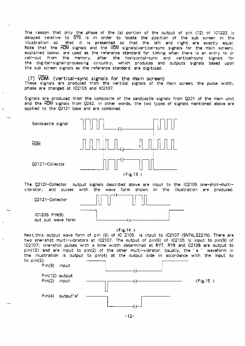
The reason that only the phase of the (a) portion of the output of pin (12) of IC1222 isdelayed relative to ~ is in order to locate the position of the sub screen in theillustration so that it is presented so that the left and right are exactly equal.Note that the ~M signals and the V~ signals(vertical-sync signals for the main screen),explained below, are used as the reference standard for timing when there is an entry to orcall-out from the memory, aft er the horizontal-sync and vertical-sync signals forthe digital-signal-processing circuitry, which produces and outputs signals based uponthe sub screen signals as the reference standard, are digitized.
(7) ~: (vertical-sync signals for the main screen)These signals are produced from the vertical signals of the main screen; the pulse width,phase are changed at IC2105 and IC2107.
Siiznals are croducedan~ the ~ signals
z applied to the Q2121
Sandcastle signal
=M
Q2121-Collector
The Q2121-Collector
from the composite of the sandcastle signals from Q221 of the main unitfrom Q242, In other words, the two types of signals mentioned above arebase and are combined.
u-u-11-~J-u-lrll/I
(I
Jl_l-lrm<Fig,13 >
output signals described above are input to the IC2105 one-shot-multi-vibrator, and pulses with the wave form shown in the illustration are produced.
Q2121 -Collectorm~
LIC1205 PIN(6)out put wave form ~,—~’
<Fig,14 >Next, this output wave form of pin (6) of IC 2105 is input to IC2107 (SN74LS221N). There aretwo one-shot multi-vibrators at IC2107. The output of pin(6) of IC2105 is input to pin(9) ofIC21 07; one-shot pulses with a time width determined at RY7, RY8 and C2108 are output topin(l 2) and are input to pin(2) of the other multi-vibrator. Usually, the ‘ a ‘ waveform inthe illustration is output to pin(4) at the output side in accordance with the input toto pin(2).
Pin(9) inputLf~
Pin(12) outputPin(2) input
~~
<Fig.15 >
Pin(4) output” a“
~r
-12-

In addition to the above, sync signals separated frompin(1) after passing through Q2107 and Q2128.
Q2107-E sync-separationoutput
Q2128-collector till ‘+-lI UUUL
Pin (4)
If the VTR
output”b” I
the video signals are applied to
~
1
r
<Fig.16> ~ I
sync signals (particularly the horizontal-sync signals) being input are disturbedor are small, the phase of the sandcastle signals is delayed, and, as shown in thei Ilustrat ion (the broken line portion of the(a) output in the illustration below), theupslope is delayed.When this happens, the phase relationship with ~M is not maintained and vertical jitteroccurs, and for that reason the pulses resulting from the sync signals input from pin(1) atthat time are given priority, thereby preventing output.
In addition, because vertical jitter occurs when ~ signals are not within the ‘ A’period of the illustration as a result of the relationship of ~M and VDIFl signals, the ~signals are maintained during that period.
Pin (4) output (a)~5 e,
Pin (4) output (b) \)
!
[~ j <Fig.17>/!
Although the output of pin(4) is usually (a), the phase deviates as shown by the broken lineof the (a) output in the illustration above if the sync signals (special types ofVTR signals, etc. ) are not normal. Because, at that time, the deviation of the phasefrom the S~ signals is of large magnitude, thus resulting in vertical jitter, the output ofpin(4) (b) is given priority at this time, and the (b) output signals are used.
-13-
—
312.5Hl-VERT, FIELD
23,5H :
f
I
, i I
n picture area
Range of imagesfor reproductionscreen.
(shaded area)of the PIP
I
T‘ p ““r”’(
< FIG.18> Range of video-imagesentered in the memory
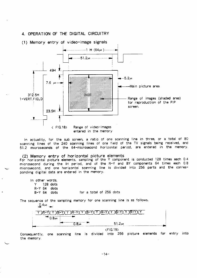
screen, a ratio of one or a total of 80In actuality, for the sub scanning Iine in three,scanning I ines of the 240 scanning lines of one field of the TV signals being received, and51,2 microseconds of the 64-microsecond horizontal period, are entered in the memory.
(2) Memory entry of horizontal picture elementsFor horizontal picture elements, sampling of’ the Y component is conducted 128 times each 0.4microsecond during the IH period, and of the R-Y and BY components 64 times each 0.8
L microsecond, and one horizontal scanning Iine is divided into 256 parts and the corres-
ponding digital data are entered in the memory.
,In other words,
Y 128 dotsR-Y 64 dots
s B-Y 64 dots for a total of 256 dots
The sequence of the sampling memory for one scanning line is as follows.JJ.4p5 *
Y -Y Y ~Y Y -Y Y B-YX Y XR-W-YX Y XR-Yx Y-~k{:8k~: x ..w& x x ,
,,
-14-
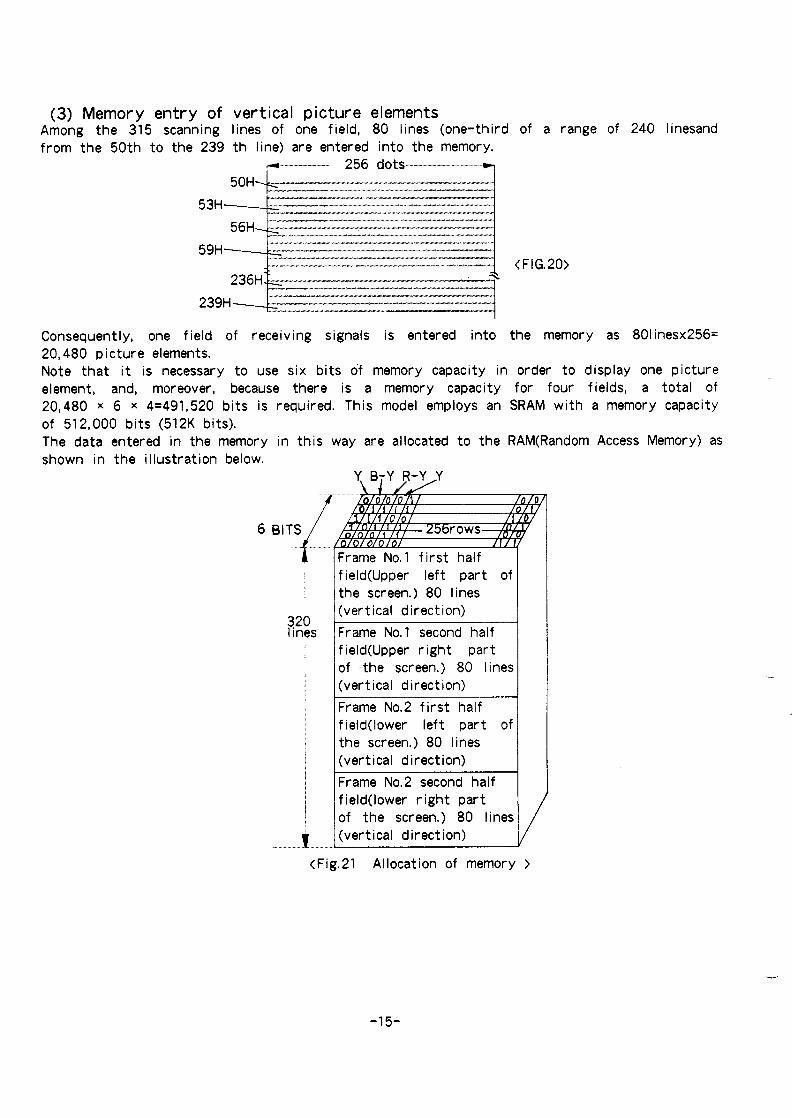
(3) Memory entry ofAmong the 315 scanningfrom the 50th to the 239
vertical picture elementslines of one field, 80 lines (one-third of a range of 240 linesandth Iine) are entered into the memory.
236HL ------%.-.—”/-,-....—.—-....”—...-
—n.——— “/.———..-..,,/,..—..——
Consequent Iy, one field of receiving signals is entered into20,480 picture elements.
<FIG!20>
the memory as 801inesx256’
Note that it is necessary to use six bits of memory capacity in order to display one pictureelement, and, moreover, because there is a memory capacity for four fields, a total of20,480 x 6 x 4=491,520 bits is required. This model employs an SRAM with a memory capacityof 512,000 bits (512K bits).The data entered in the memory in this way are allocated to the RAM(Random Access Memory) asshown in the illustration below.
Y B~Y R-Y .Y
6 BITS
field(Upper left part ofthe screen. ) 80 Iines(vertical direction)
Frame No.1 second halffield(Upper right partof the screen. ) 80 lines(vertical direction)
Frame No.2 first halffield(lower left part ofthe screen. ) 80 Iines(vertical direction)
Frame No,2 second halffield(lower right partof the screen. ) 80 Iines(vertical direction)
<Fig,21 Allocation of memory >
-15-

—
L
.
i
4-1 A/D CONVERTER ( ICI 203, M52686FP)The Y, R-Y and B-Y signals that were separated from the video signals at IC1201(M51308SP)are input to pins(6),(7) and (8) of the A/D converter (IC1203,M52686FP).They are AC-coupled, and DC bias is added at R1222,R1223 and R1224.These analog input signals are subjected to division by 64 (from the signal’s level 2.75V to3.75 V), and each individual input voltage is converted to a six-bit digital value.The Y, R-Y and B-Y signals that were converted to six-bit digital values are output toB1 -66(P insl 7-22).
‘M~-V input I
I1 MD conwrtu I“
[
Y
1
01010
6BITS
[
B-Y
o01010
[
Y
1
1
001
0[
Y
o01
01
1
6BITS 6BITS 6BITS 6BITSClulllpPUIS*
Multlpl*x*r I
i
<FIG.22> A/D CONVERTER
This output is output in the following sequence: Y+ B-Y+ Y +R-Y +Y +B-Y each as a six-bitdigital signal, and is stored in the SRAM(Static Random Access Memory).
(1) Multiplexer signalsThe multiplexer signals are signals that are output from the PIP controller (I C1201,M50541 FP); these signals function to determine the sampling order of conversion at the A/Dconverter.In other words, when MPX-Y is HIGH level, the Y signals are sampled and A/D converted. WhenMPX-R is HIGH level, the R-Y signals are sampled and A/D converted.When MPX-B is HIGH level, the B-Y signals are sampled and A/D converted .These MPX signalsare one after another converted to HIGH level in the sequence Y, R, Y, B and Y.
(2) SLC (pin 15): (sampling clamp pulses)The SCL pulses are output from IC1201 (M50541FP). These are signals that determine the
period of the pedestal level; when these signals are HIGH level, the signals input to theA/D converter are clamped.
-16-
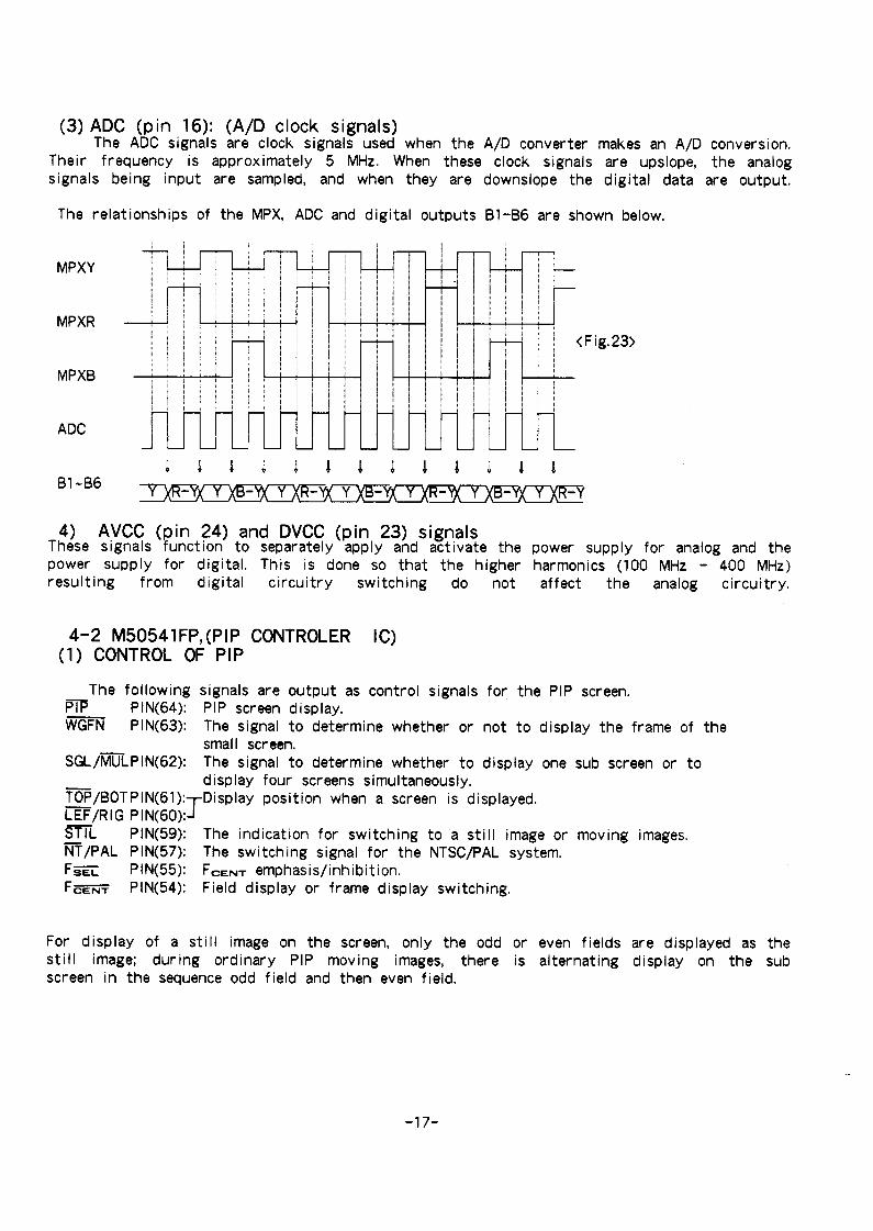
(3) ADC (pin 16): (A/D clock signals)The ADC signals are clock signals used when the A/D converter makes an A/D conversion.
Their frequency is approximately 5 MHz. When these clock signals are upslope, the analogsignals being input are sampled, and when they are downslope the digital data are output,
The relationships of the MPX, ADC and digital outputs B1-B6 are shown below.
MPXY
MPXR
MPXB
ADC
B1-B6
ig.23>
4) AVCC (pin 24) and DVCC (pin 23) signalsThese signals function to separately apply and activate the power supply for analog and thepower supply for digital. This is done so that the higher harmonics (100 MHz - 400 MHz)resulting from digital circuitry switching do not affect the analog circuitry.
4-2 M50541FP, (PIP CONTROLER IC)(1) CONTROL OF PIP
The followingPT PIN(64):m PIN(63):
SGL/~LP IN(62):
signals are output as control signals for the PIP screen.PIP screen display.The signal to determine whether or not to display the frame of thesmal I screen.The signal to determine whether to display one sub screen or todisplay four screens simultaneous y,
=P/BOTPlN(61): Display position when a screen is displayed.=/RIG p IN(60): T
~L PIN(59): The indication for switching to a still image or moving images.~T/PAL PIN(57): The switching signal for the NTSC/PAL system.F= PIN(55): Fc~~~ emphasis/inhibition,F= PIN(54): Field display or frame display switching,
For display of a still image on the screen, only the odd or even fields are displayed as thestill image; during ordinary PIP moving images, there is alternating display on the subscreen in the sequence odd field and then even field.
-17-

—
.
,-
(2) Sync signalsIn order to activate the PIP operation, sync signals ~S ~S and ~S, which are producedfrom the video signals for the sub screen, and sync signals ~, VDM, and HDM, which areproduced from the video signals for the main screen, are input to this IC,
The wave form for each of these signals is shown in the figures below.
“1111 - - - ,lA _ .1
~! !
+1 H --A
. T-1<FIG.24>
The phase relationships are as shown above. When there is a change of the phase relation-sip of ~S and VDS,or of SYM and VDM, the determination of odd and even fields changes andthe screen images become abnormal, and for that reason it is important for the phaserelationship to be maintained,Note that, even though the phase of ~S and HDS and of ~M and ~M change, only the positionin the lateral direction of the sub screen changes,
SYM ‘br~ - - “ .,_ J _ll
& ~~~-------1 v---- .--...-.-.........ti
<FIG.25)
(3) Control of the A/D converter (M52686P)The signals that control the A/D converter are MPXY,MPXR, MPXB, ADC and SCL; for
additional details, refer to section 4-1, All of the above signals are output fromM50541 P, and these signals are produced and emitted by SCLK, ~S, ~S and ~
(4) Control of the memory (M5M4C500L)The signals that control the memory are SIC, SOC, AO -A7, etc.
sic : This is the timing signal that enters the B1 - B6 data into the memory,Soc : This is the timing signal that takes out the DI - D6 data from the memory.AO-A7: These are the signals that designate the memory address; these signals
indicate the timing of SIC and SOC.
-18-
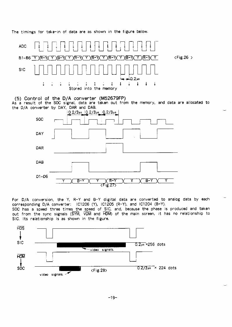
The timings for take-in of data are as shown in the figure below.
~~c FJ:J’JJJJJJJJJJJJJ_
SlcL +,
<Fig.26 >
(5) Control of the D/A converter (M52679FP)As a result of the SOC signal, data are taken out from the memory, and data are allocated tothe 13/A converter by DAY, DAR and DAB.
(). 2/3Ps ‘ 0. 2/3,F&..?2?Fs~~ ......
Soc -1.L7d7ru-uDAY
DAB
I L 1 1
D1-D6Y x B-Y x. Y x Y x B-Y x Y
For D/A conversion, the Y, R-Y and B-Y digital data are converted to analog data by each –correspond ing D/A converter: IC1206 (Y), IC1205 (R-Y), and IC1204 (B-Y).SOC has a speed three times the speed of S1C, and, because the phase is produced and taken——out from the sync signals (SYM, VDM and HDM) of the main screen, it has no relationship toSIC. Its relationship is as shown in the figure.
Slc
m
iSoc
‘video signals.
l~ru
~/ ~ x 224 dots
,/video signals.
-19-
.
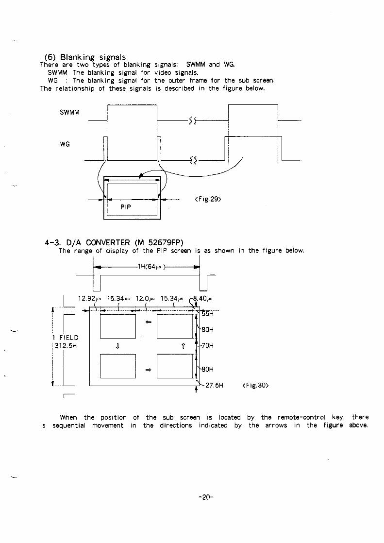
(6) Blanking signalsThere are two types of blanking
SWMM The blanking signal forWG : The blanking signal for
The relationship of these signals
r
signals: SWMM and WG.video signals.the outer frame for the sub screen.is described in the figure below.
1 I I
SWMM
WG
4-3. D/A CONVERTERThe range of display
(M 52679FP)of the PIP screen is as shown in the figure below.
~1H(64” )-4
.
.
I1 F’IELD312.5H
u u
2.92Ps 15.34Ps 12.OPS 15,34Pm+ .., 1.A.. J.. .....- ........1........+ J W ~
D “ ml: ~“’””
r--
When the positionis sequential movement
of the sub screen is locatedin the directions indicated by
<Fig.30>
by the remote-control key, therethe arrows in the figure above.
-20-
(1) Number of display picture elements in the horizontal direction of the subscreen.
For the sub screen, the number of picture elements are displayed:
Inscanning
Y :112 dotsR-Y :56 dotsB-Y :56 dotsFRAME :3+3 dotsTotal :230 dots
this way, for the horizontal direction (and including the frame display) oneI ine is displayed by 230 dots. In other words, there are 112 dots for the y
component (one dot every 0.133 microsecond). For the R-Y component and the B-Y component, thescreen is composed of picture elements of 56 dots each (one dot every 0.266 micro- second)for R-Y and B-Y.
(2) Sub-screen vertical direction displayThe video portion in the vertical direction is displayed by 78 scanning lines
and two scanning lined for the up/down frame portion.
(3) D/A converter operationThe digital signal data taken out from the memory by the SOC (the call-out clock
signal) are input to pins (18) - (13) of the D/A converters. Each of the individual D/Aconverters(l C1204, IC1205 and IC1206) perform sampling independently by DAB, DAR and DAY,and convert the signals. Because the operation of each of these three ICS is fundamental Iythe same, here we will explain only IC1206. The Y signals are sampled by DAY (the samplingclock signal) when input to pin(12); only the Y signals are taken into the converter, wherethey are converted to analog Y signals and then output to pin(4).
(3)-1. BLK: Pin (6) blanking signalsThese are signals that function to regulate whether or not the converted analog v
signals are output. Here, the analog signal for the period of the SWMM signal is output.
Blanking signal(SWMM)
* .....& . .
Analog signal output ,Analog signal is not output
(3)-2. INV (pin (7)): invert controlThis determines the polarity of Y signal output. When this signal is LOW level,positive-polarity signals are output.
(3)-3. COMP (pin (9)): comparateThis terminal performs phase correction between the Y, R-Y and B-Y signals; adjustmentis possible by the capacitor’ s capacity.
(3)-4. BE1 and BE2 (pins (19) and (20)): bit ableThese terminals select whether Dl, D3, D4 and D5 (among D1 - D6) will be used or not.Because al I six bits are used here, these terminals are connected to ground. (not used)
(3)-5. VRB, VRM and VRT (pins (1), (5), (8))These terminals are used to set the Y signal’reference voltage supplied from IC1203 M52686FP.
VRB: 3.25VVRM: 3.75VVRT: 4.25V
-21-
s analog value voltage by the standardThey are set to:
Fundmmtal clock
—--
08eillctal+o.zmw 45Mllz Vco O#clllQtOr
Ill”-—
<Fig,32 A/D, D/A Converter>
-22-

whiteThe Y
4,25V
3.75V
3.25V
For the Y signal, centered at 3.75V and with the black level 100% 3.25V and thelevel 100% 4.25V, conversion is to amplitude 1,OVP-P analog signal vOltage
signal is restored, maintaining the relationship described above.
VRT ~~~~~~----------------- whit e level 100%
VRM -
h.VRB - -- black level 100%
<Fig.33>
!
.w---I12b its ---~Digital dataD1-’D6
...........r
Y SIGNAL 1.OVPP!
T
k-- ~~ 15.34P .-’+
<Fig.34>
-23-
L
,
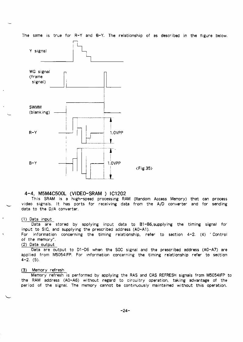
The same is true for R-Y and B-Y. The relationship of as described in the figure below.
Y signalhI’1t I
B-Y<Fig.35)
4-4, M5M4C500L (V IDEO-SRAM ) ICI 202This SRAM is a “high-speed processing RAM (Random Access Memory) that can process
video signals. It has ports for receiving data from the A/D converter and for sendingdata to the D/A converter.
(1) Data irmut. .Data are stored by applying input data to 61 -B6, supplying the timing signal for
input to SIC, and supplying the prescribed address (AO-A1 ).For information concerning the timing relationship, refer to section 4-2. (4) ‘ Controlof the memory”.(2) Data output
Data are output to D1-D6 when the SOC signal and the prescribed address (AO-A7) areapplied from M50541FP. For information concerning the timing relationship refer to section4-2, (5).
(3) Memory refreshMemory refresh is performed by applying the RAS and CAS REFRESH signals from M50541FP to
the RAM address (AO-A6) without regard to circuitry operation, taking advantage of theper iod of the signal. The memory cannot be continuously
L
maintained without this operation.
-24-

4-5. SN74S124 (5-MHZ VCO OSCILLATION CIRCUITRY) IC1208With the incorporated resistance and C1238 connected to pins 4 and 5 as the
time-constant, this circuitry oscillates 5 MHz. This is used mainly for display of thescreen, Adjustment is by VR1201. When this is changed, the amplitude in the lateraldirect ion of the sub screen video images is changed. VCOE is a sync signal produced basedupon ~ and VDM; the 5.O-MHZ phase is regulated by this signal.
VCOE
‘n--
...........64W ...–– .
-n
~ -— 7“i 5-MHZ osci IIat ion \ Reset per iod~period i
<Fig.36>
SCLK (5 MHz) is output from the pin (7) and is input to pin (11) of IC1201 M50541FP.R1202 and R1203 are for setting the bias of the oscillation circuitry. Q1202 functions todetect the level of VCOE as a result of changes of the thermal drift, etc., and appliesnegative feedback to pin (2). By doing so, changes of the thermal drift are suppressed, andchanges in the amplitude in the horizontal direction are also inhibited.
4-6, 30-MHZ OSCILLATORSOsci Ilation is performed by using the ceramic oscillator and one gate of IC1207
MC74HCU04DW. The reason for multiple connections of the gate is so as to maintain the 1:1pulse duty. This signal is the system’ s fundamental clock signal; it is emitted (togetherwith sync signals) when the M50541FP sub screen signals are taken in, and also functions toactivate other operations within the IC.
<Fig.37>
f
C1233I0EM47
1MHZ OSCK0272X0 ~
—
CL.K SIGNAL30. OMHZ
-25-
—
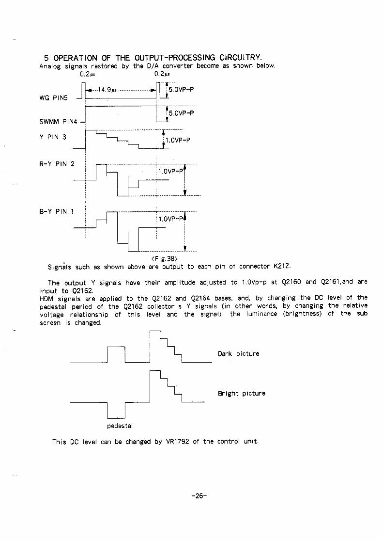
5 OPERAT 10N OF THE OUTPUT-PROCESSING CIRCUITRY.Analog signals restored by the D/A converter become as shown below.
0.2P o.2w
<Fig.38>Sign~ls such as shown above are output to each pin of connector K21Z.
—
The output Y signals have their amplitude adjusted to l. OVp-p at Q2160 and Q2161, and areinput to Q2162.HDM signals are applied to the Q2162 and Q2164 bases, and, by changing the DC level of thepedestal period of the Q2162 collector’ s Y signals (in other words, by changing the relativevoltage relationship of this level and the signal), the luminance (brightness) of the sub
screen is changed.
n
--nJ L ‘ark‘icture
1>
Bright picture
I I
pedestal
This DC level can be changed by VR1792 of the control unit.
—
-26-
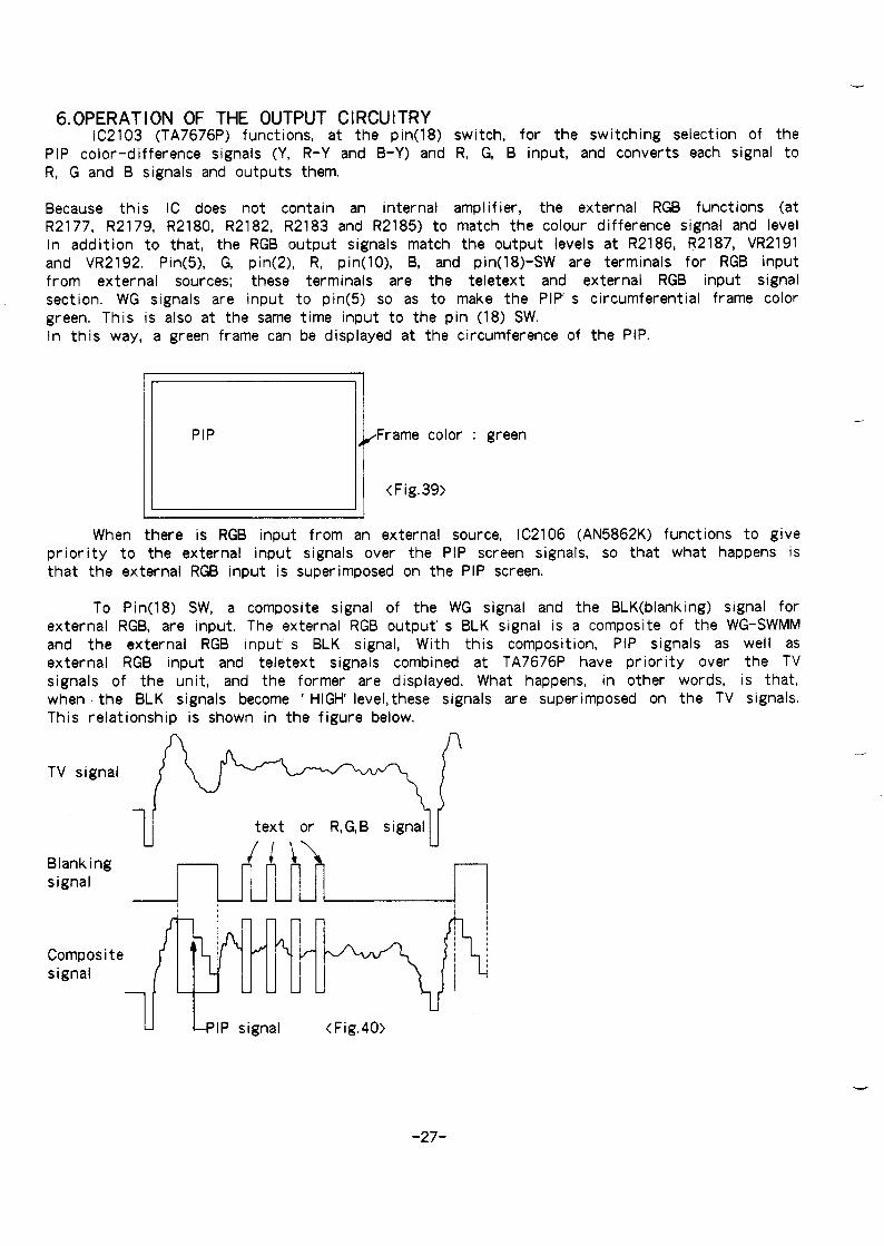
6. OPERATION OF THE OUTPUT CIRCUITRYIC2103 (TA7676P) functions, at the pin(18) switch, for the switching selection of the
PIP color-difference signals (Y, R-Y and B-Y) and R, G, B input, and converts each signal toR, G and B signals and outputs them.
Because this IC does not contain an internal amplifier, the external RGB functions (atR2177, R2179, R2180, R2182, R2183 and R2185) to match the colour difference signal and levelIn addition to that, the RGB output signals match the output levels at R2186, R2187, VR2191and VR2192. Pin(5), G, pin(2), R, pin(l O), B, and pin(18)-SW are terminals for RGB inputfrom external sources; these terminals are the teletext and external RGB input signalsection. WG signals are input to pin(5) so as to make the PIP s circumferential frame colorgreen. This is also at the same time input to the pin (18) SW.In this way, a green frame can be displayed at the circumference of the PIP.
PIP
f
Frame color : green
.~ ‘Fig-3g>When there is RGB input from an external source, IC2106 (AN5862K) functions to give
priority to the external input signals over the PIP screen signals, so that what happens isthat the external RGB input is superimposed on the PIP screen.
To Pin(18) SW, a composite signal of the WG signal and the BLK(blanking) signal forexternal RGB, are input, The external RGB output s BLK signal is a composite of the WG-SWMMand the external RGB input’ s BLK signal, With this composition, PIP signals as well asexternal RGB input and teletext signals combined at TA7676P have priority over the TVsignals of the unit, and the former are displayed. What happens, in other words, is that,when the BLK signals become ‘ HIGH Ievel, these signals are superimposed on the TV signals.This relationship is shown in the figure below.
TV signal
-[
Blankingsignal
Compositesignal /
text or R,G,B signal I
-!M_iDL
UIP signal <Fig.40>
-27-
L
41111 GI x
I I I
1 I 1 1
-1
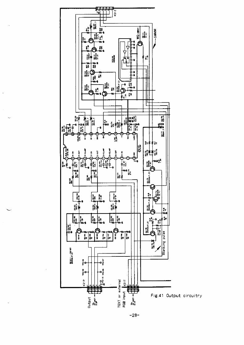
Fig.41 Output circuitry
-28-
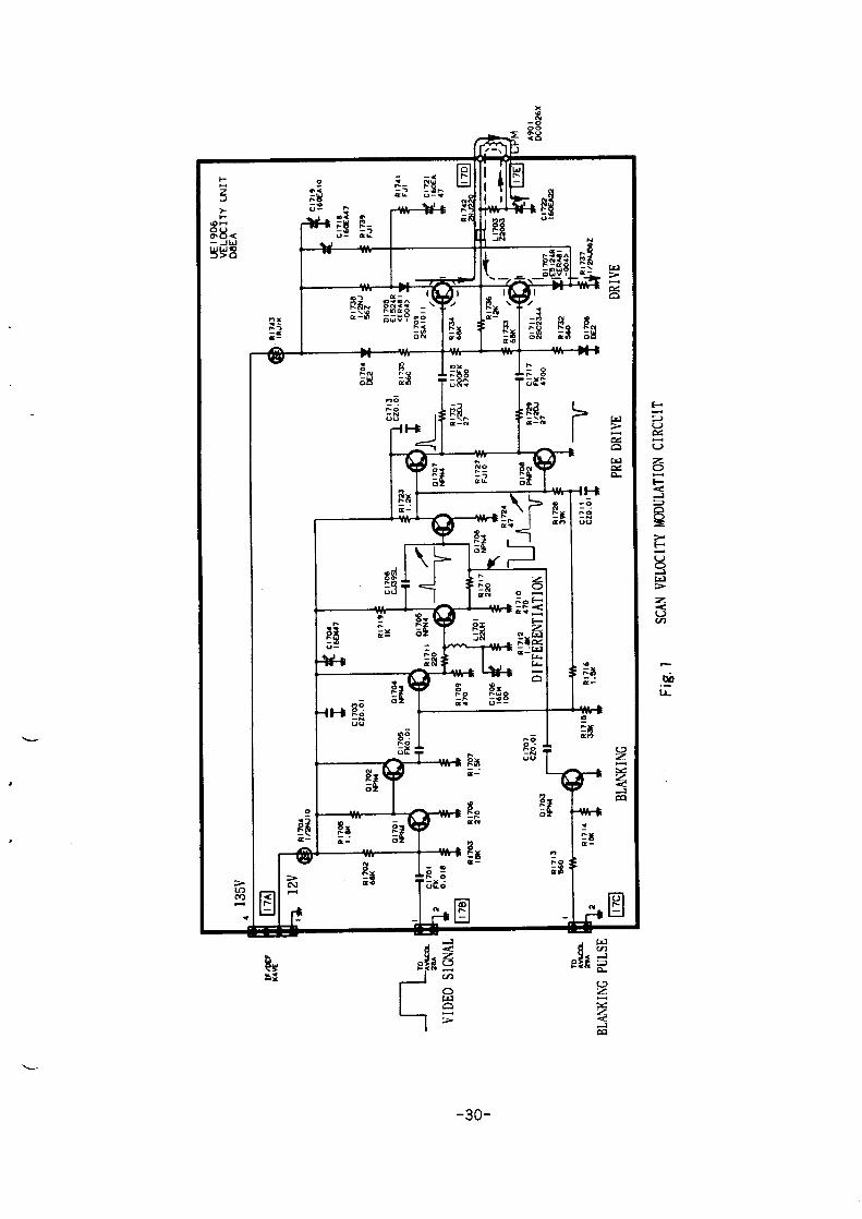
SCAN VELOCITY MODULATION CIRCUITRY (FOR E3-B CHASSIS)
(1) OUT LINESVM (Scan Velocity Modulation) is the circuitry to improve the picture resolution
by changing the electron beam scan velocity and, it can emphasis the brightness change of
the contour of the picture.The rapid scan velocity of the electron beam makes the period of activating the fluorescentface to be shorter and the brightness to be lower.The delayed scanning velocity makes the brightness of the fluorescent to be brighter.
Because this system is not to change the volume of the beam current itself, it does not
degrade the focus quality.
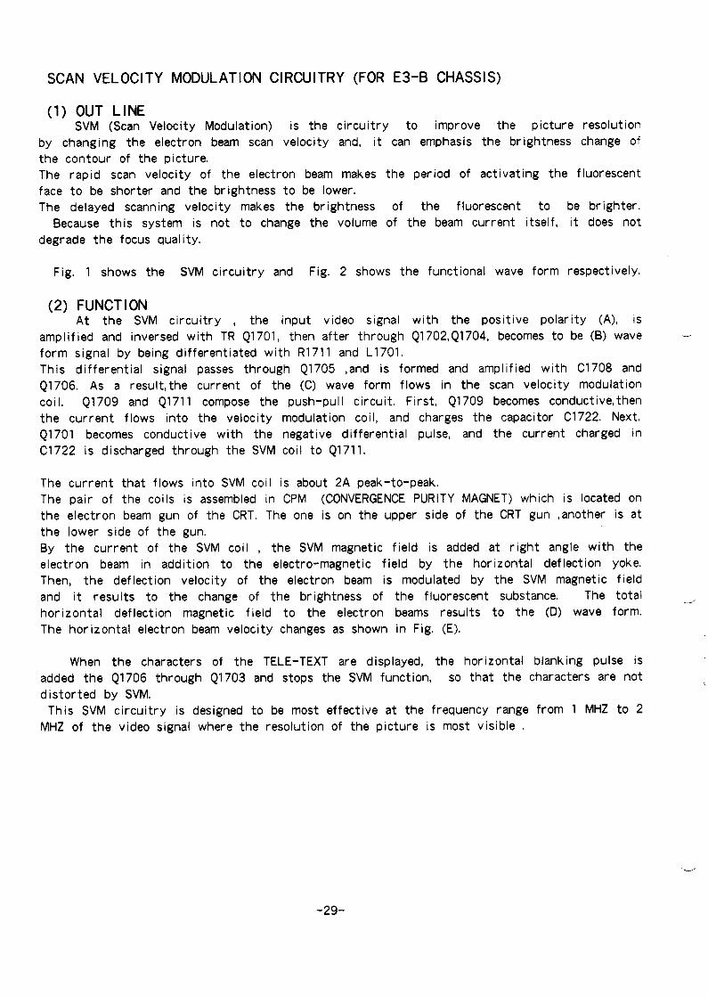
Fig. 1 shows the SVM circuitry and Fig. 2 shows the functional wave form respectively.
(2) FUNCTIONAt the SVM circuitry , the input video signal with the positive polarity (A), is
amplified and inversed with TR Q1701, then after through Q1702,Q1704, becomes to be (B) wave —
form signal by being differentiated with R1711 and L1701.This differential signal passes through Q1705 ,and is formed and amplified with C1708 and
Q1706. As a result, the current of the (C) wave form flows in the scan velocity modulation
coil. Q1709 and Q1711 compose the push-pull circuit. First, Q1709 becomes conduct ive, then
the current flows into the velocity modulation coil, and charges the capacitor C1722. Next,Q1701 becomes conductive with the negative differential pulse, and the current thawed inC1722 is discharged through the SVM coil to Q1711.
The current that flows into SVM coi I is about 2A peak-to-peak.The pair of the coils is assembled in CPM (CONVERGENCEPURITY MAGNET) which is located on
the electron beam gun of the CRT. The one is on the upper side of the CRT gun ,another is atthe lower side of the gun.By the current of the SVM coil , the SVM magnetic field is added at right angle with theelectron beam in addition to the electro-magnetic field by the horizontal deflection yoke.Then, the deflection velocity of the electron beam is modulated by the SVM magnetic field
and it results to the change of the brightness of the f Iuorescent substance. The total _horizontal deflection magnetic field to the electron beams results to the (D) wave form.The horizontal electron beam velocity changes as shown in Fig. (E).
When the characters of the TELE-TEXT are displayed, the horizontal blanking pulse is
added the Q1706 through Q1703 and stops the SVM function, so that the characters are notdistorted by SVM.
This SVM circuitry is designed to be most effective at the frequency range from 1 MHZ to 2MHZ of the video signal where the resolution of the picture is most visible .
w
-29-
(L o I
-n,.
VID
EOS&
Al m Avu
n.
BLAN
KIN
GP~
LSI
..
(
l.E19
06
,13
5VV
ELO
CIT
YUN
ITD
8EA
m,
RI74
3IR
JIK
~12
VR
1704
l/2t4
Jto
1 x
C17
04
:17&
mI6
m47
C17
03
R&
702
::
Czo
.o
l00
m2
a
0170
1C
17C
5F
Ko
.o
l,,
*10,
.,(
15C
M1
-R
1703
R17
02R
I70
7,
.,”0170
4C
1708
C.D
%i
C17
13
,.R
1723
Czo
.o
l
1.2K
“Y
+
-.,7
$$L
W20
9R
1731
l/2o
J27
{OK
27
01.5
)(
nrC
1719
-16
0EA
I0
C17
1816
caA
47R
1738
0170
41/
2?4.
!06
zR
1739
FJ
I
R&
m
14
DI70
5:;
::::
-004
>
0170
92S
4101
1/-
IR
1736
“\6e
u-
wr
-
C17
0771
~2
Czo
.ol
~lo
0170
3D
IFFE
REN
TIAT
ION
.R
1713
.,I
540
h&
728
R17
18
ml
BLAN
KIN
GPR
ED
RIV
E
..C
1715
&&
K+
-it--
C!7
17F
K 4700
m,91
-#4
----
-
L17
03
izz
cv-*
rfM
33,-
,h
17E
0171
1~
_~=3
641- 01
707
C17
22
R17
32Im
lwfl
1~
-004
>
DR
IVE
$\ ) .MA
90I
0CO
026X
Fig,
1SC
ANV
EL
OC
ITYM
OD
UL
AT
ION
CIR
CU
IT

Fig.2 Scan Velocity Modulation wave forms
(a)
(b)
(c)
(d)
(e)
(f) -r,“,;
Video input signal!I
r Differentiated wave form
J;
I
I
I
Current wave form in~ ~VM ~oil
‘,./J
Horizontal deflection
magnetic field
/+Horizontal deflection velocity
+
The brightness change of
fluorescent substance on the CRT
-31-