cnfet: an alternative to conventional … performance of a cnfet based cccii is compared with the...
TRANSCRIPT

International Research Journal of Engineering and Technology (IRJET) e-ISSN: 2395 -0056
Volume: 03 Issue: 06 | June-2016 www.irjet.net p-ISSN: 2395-0072
© 2016, IRJET | Impact Factor value: 4.45 | ISO 9001:2008 Certified Journal | Page 2859
CNFET: AN ALTERNATIVE TO CONVENTIONAL MOS FOR ANALOG
APPLICATIONS.
Mohd Mohsin1, M Y Yasin2,Irshad Ali3,Umar Mohammad4
1,3,4M.Tech. Scholars, 2Faculty member, Department of Electronics and Communication Engineering,
IntegralUniversity, Lucknow, India
Abstract- Bulk CMOS has played a great role in VLSI,
because it yielded to the device scaling. Therefore, it was
considered as bench mark technology so far. But
unfortunately, it seems that the scaling of CMOS is almost
saturated, leaving thereby no much space for future.
Apparently, carbon nanotube FETs (CNTFET) show
potential to take up the challenge for future VLSI growth.
Literature shows that the CNTFETs are a good alternative.
They can cope up with further scaling and are said to be
low power device. In this paper, second generation current
controlled current conveyors (CCCII) based on both bulk
CMOS and CNTFETs are studied.A CCCII is an important
analog device and can be found as being used in numerous
applications on filters, oscillators, amplifiers etc. In this
paper we analyse the performance of bulk CMOS based
analog circuitsand compare it with thecorresponding
CNTFET based alternative. The study is performed by
simulating the two circuits on HSPICE involving the latest
device model parameters. Simulation results satisfactory.
Keywords: CNTFET and MOSFET, Current Conveyor,
CNTFET based CCCII, a Comparison between CMOS
based CCCII and CNFET based CCCII,
1. INTRODUCTION
Modern VLSI concentrates on application like
system on chip, portable electronic gadgets and
embedded systems, especially medical
implantations of VLSI. All such applications are
power sensitive applications. Power is already
considered as a design parameter [1]. Efforts are
required to reduce power as far as it is possible. So
far the MOSFET has been a device favouring the
VLSI upward growth because of it's ability to cope
with the harsh scaling. Device scaling also resulted
in scaling down the power of the circuits as well [2].
But it ispity that the scaling apparently seems to be
incapable to cope with scaling any further [2].
Therefore, the designers are looking for
alternatives so that the power and complexity
problems are successfully tackled. One such
alternative is to use carbon nanotubesas channel in
MOSFETS instead of the bulk silicon channel [6].
This results into a totally new device named as
carbon nanotube FET or CNTFET or CNFET. It is
expected that this incorporation of nanotubes may
add a few advantages to the conventional CMOS,
like reduced power, higher speed operation and
higher frequency of operation and reduced
parasites [6].
Silicon has so far been in use as an important
semiconductor material because of it’s striking
characteristics, and its importance is still
considered. Silicon bulk devices characteristics are
still considered as benchmark [3].Therefore it is
imperative to compare any new device
characteristics with the similar bulk silicon device.
In this paper, CNFETs are used in complementary
mode to design the second generation current
controlled current conveyor (CCCII), which is a
popular analog VLSI device. This device shows
remarkable performance in analog designs and
therefore it is considered here. The performance of
a CNFET based CCCII is compared with the normal
bulk CMOS based CCCII, and shows satisfactory
results.
2. CARBON NANOTUBE FET’s (CNFET’s):
Carbon nanotubes are cylindrical nanostructures
and exhibit some extraordinary electrical and
mechanical properties which mainly rely onits
layer structure. Multi wall structure are easier to
form but show inferior characteristics, however,

International Research Journal of Engineering and Technology (IRJET) e-ISSN: 2395 -0056
Volume: 03 Issue: 06 | June-2016 www.irjet.net p-ISSN: 2395-0072
© 2016, IRJET | Impact Factor value: 4.45 | ISO 9001:2008 Certified Journal | Page 2860
single wall structures are complicated but are
easier to handle and show good performance.
Carbon nanotube is basically made by wrapping a
honey comb sheet of carbon atoms. The way the
honeycomb sheet is wrapped up is described by
indices (n,m). The indices are unit vectors in two
direction at right angle in the graphene lattice.
These indices are responsible for determining the
electrical characteristics. Thus If m = 0, the
nanotubes are called zigzag nanotubes, and
if n = m, the nanotubes are
called armchair nanotubes. Otherwise, they are
called chiral. The diameter of an ideal nanotube
can be calculated from its (n,m) indices. The
symmetry and unique electronic structure of
graphene, strongly affect its electrical properties.
For a given (n,m) nanotube, if n = m, the nanotube
is metallic; if n − m is a multiple of 3, then the
nanotube is semiconducting with a small band gap,
otherwise the nanotube is a
moderate semiconductor. Thus all armchair
(n = m) nanotubes are metallic, and nanotubes
(6,4), (9,1), etc. are semiconducting [4]. Again the
n-type and p-type characteristics are generated by
suitable dopings done to the tubes. These tubes are
used as channels in MOSFETs (CNFETs). In a
CNFET the tubes are buried under gate region and
the portion of tubes outside gate area, are doped n-
type or p-type[8]. Once n channel/p-channel
CNFETs are available they can be used in a manner
similar to the conventional CMOS. However, to run
n-CNFET p-CNFET based circuits, the device
models and device parameters are required by a
simulation software. Here in this work we have
used HSPICE therefore we use the material
supplied by nano-Hub [7].
On the basis of operation of CNTFETsfall in mainly
two types.(i) Schottky barrier CNTFET transistor,
where the source and drain junctions are metal
contacted and transportation of electrons occurs by
tunnelling through a Schottky barrier at the source-
channel junction. These transistors use direct
contact of the metal with the nanotube in their
fabrication process; hence they have Schottky
Barrier at the metal Nanotube junction. This type
has some ambipolar properties that are more
appropriate for CMOS logic families and because of
Schottky barrier, the current of ON state is low. (ii)
Ballistic type CNTFET, where the channel of
transistor is intrinsic, whereas the source and drain
are have suitable doping. An electrostatic potential
barrier, prevents flowing of electrons through the
channel. By a positive gate voltage, the barrier is
passed down and current will flow across the
semiconducting nanotube, hence ballistic CNFET is
more appropriate for MOSFET like CNTs.
3. CURRENT CONTROLLED CURRENT
CONVEYOR II (CCCII);
CCCII is considered as an important building block
among various active devices. Most of the active
devices are made by proper arrangements of CCCII.
The CCCII is different from the other two current
conveyors in the sense that it has zero current at
node Y, i.e. this node act as the high impedance
voltage node. And this node Y act as the operational
amplifier input nodes. That’s why the node Y can be
used to sense voltage signals conveniently. This
gives an advantage of not loading the input signal.
Another difference is that the low impedance input
(node X) considers an input impedance RX. This
impedance can be used as a conventional resistor in
the circuit designing, and is observed as a hardware
optimising tool [5].
4. CCCII FEATURES
If a voltage is applied to terminal Y, an equal
potential will appear on the input terminal X.
1. The current in node Y is zero.
2. The current IX will be conveyed to output
terminal Z such that terminal Z has the
same characteristics, Iz = Ix, with high
output impedance.
3. Potential of X being set by that of Y is
independent of the current being forced
into port X.
4. Terminal Y exhibits an infinite input
impedance node.
International Research Journal of Engineering and Technology (IRJET) e-ISSN: 2395 -0056
Volume: 03 Issue: 06 | June-2016 www.irjet.net p-ISSN: 2395-0072
© 2016, IRJET | Impact Factor value: 4.45 | ISO 9001:2008 Certified Journal | Page 2861
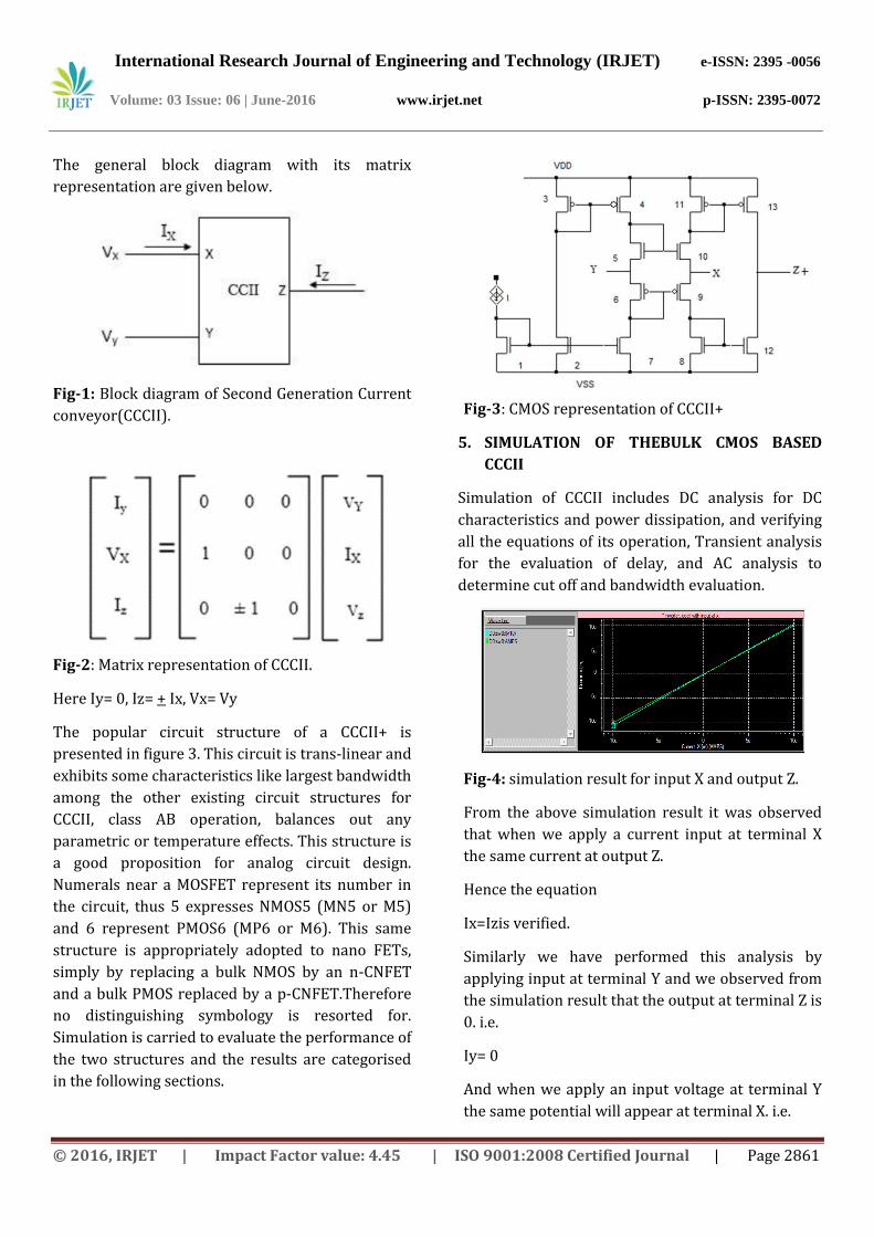
The general block diagram with its matrix
representation are given below.
Fig-1: Block diagram of Second Generation Current
conveyor(CCCII).
Fig-2: Matrix representation of CCCII.
Here Iy= 0, Iz= + Ix, Vx= Vy
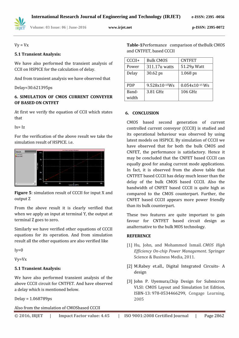
The popular circuit structure of a CCCII+ is
presented in figure 3. This circuit is trans-linear and
exhibits some characteristics like largest bandwidth
among the other existing circuit structures for
CCCII, class AB operation, balances out any
parametric or temperature effects. This structure is
a good proposition for analog circuit design.
Numerals near a MOSFET represent its number in
the circuit, thus 5 expresses NMOS5 (MN5 or M5)
and 6 represent PMOS6 (MP6 or M6). This same
structure is appropriately adopted to nano FETs,
simply by replacing a bulk NMOS by an n-CNFET
and a bulk PMOS replaced by a p-CNFET.Therefore
no distinguishing symbology is resorted for.
Simulation is carried to evaluate the performance of
the two structures and the results are categorised
in the following sections.
Fig-3: CMOS representation of CCCII+
5. SIMULATION OF THEBULK CMOS BASED
CCCII
Simulation of CCCII includes DC analysis for DC
characteristics and power dissipation, and verifying
all the equations of its operation, Transient analysis
for the evaluation of delay, and AC analysis to
determine cut off and bandwidth evaluation.
Fig-4: simulation result for input X and output Z.
From the above simulation result it was observed
that when we apply a current input at terminal X
the same current at output Z.
Hence the equation
Ix=Izis verified.
Similarly we have performed this analysis by
applying input at terminal Y and we observed from
the simulation result that the output at terminal Z is
0. i.e.
Iy= 0
And when we apply an input voltage at terminal Y
the same potential will appear at terminal X. i.e.
International Research Journal of Engineering and Technology (IRJET) e-ISSN: 2395 -0056
Volume: 03 Issue: 06 | June-2016 www.irjet.net p-ISSN: 2395-0072
© 2016, IRJET | Impact Factor value: 4.45 | ISO 9001:2008 Certified Journal | Page 2862
Vy = Vx
5.1 Transient Analysis:
We have also performed the transient analysis of
CCII on HSPICE for the calculation of delay.
And from transient analysis we have observed that
Delay=30.621395ps
6. SIMULATION OF CMOS CURRENT CONVEYER
OF BASED ON CNTFET
At first we verify the equation of CCII which states
that
Ix= Iz
For the verification of the above result we take the
simulation result of HSPICE. i.e.
Figure 5: simulation result of CCCII for input X and
output Z
From the above result it is clearly verified that
when we apply an input at terminal Y, the output at
terminal Z goes to zero.
Similarly we have verified other equations of CCCII
equations for its operation. And from simulation
result all the other equations are also verified like
Iy=0
Vy=Vx
5.1 Transient Analysis:
We have also performed transient analysis of the
above CCCII circuit for CNTFET. And have observed
a delay which is mentioned below.
Delay = 1.068789ps
Also from the simulation of CMOSbased CCCII
Table-1Performance comparison of theBulk CMOS
and CNTFET, based CCCII
CCCII+ Bulk CMOS CNTFET
Power 311.17u watts 51.29µ Watt
Delay 30.62 ps 1.068 ps
PDP 9.528x10⁻¹⁵Ws 0.054x10⁻¹⁵ Ws
Band-
width
3.81 GHz 106 GHz
6. CONCLUSION
CMOS based second generation of current
controlled current conveyor (CCCII) is studied and
its operational behaviour was observed by using
latest models on HSPICE. By simulation of CCCII we
have observed that for both the bulk CMOS and
CNFET, the performance is satisfactory. Hence it
may be concluded that the CNFET based CCCII can
equally good for analog current mode applications.
In fact, it is observed from the above table that
CNTFET based CCCII has delay much lesser than the
delay of the bulk CMOS based CCCII. Also the
bandwidth of CNFET based CCCII is quite high as
compared to the CMOS counterpart. Further, the
CNFET based CCCII appears more power friendly
than its bulk counterpart.
These two features are quite important to gain
favour for CNTFET based circuit design as
analternative to the bulk MOS technology.
REFERENCE
[1] Hu, John, and Mohammed Ismail. CMOS High
Efficiency On-chip Power Management. Springer
Science & Business Media, 2011.
[2] M.Rabey et.all., Digital Integrated Circuits- A
design
[3] John P. Uyemura,Chip Design for Submicron
VLSI: CMOS Layout and Simulation 1st Edition,
ISBN-13: 978-0534466299, Cengage Learning,
2005

International Research Journal of Engineering and Technology (IRJET) e-ISSN: 2395 -0056
Volume: 03 Issue: 06 | June-2016 www.irjet.net p-ISSN: 2395-0072
© 2016, IRJET | Impact Factor value: 4.45 | ISO 9001:2008 Certified Journal | Page 2863
[4] Lu, X.; Chen, Z. (2005). "Curved Pi-Conjugation,
Aromaticity, and the Related Chemistry of Small
Fullerenes (C60) and Single-Walled Carbon
Nanotubes". Chemical Reviews 105 (10): 3643–
3696. doi:10.1021/cr030093d.
[5] Mohd Yusuf Yasin, Bal Gopal, High Frequency
Oscillator Design Using a Single 45nm CMOS
Current Controlled Current Conveyor (CCCII+)
with Minimum Passive Components,
DOI:10.4236/cs.2011.22009, published
by Circuits and Systems, Vol.2 No.2, 2011
[6] Sethi, Rishika, and Gaurav Soni. "Power analysis
of Si MOSFET and CNFET based logic gates." Int.
J. Eng. Manag. Sci.(Alied Journals IJEMS)2.5
(2015).
[7] Ewels, Chris, et al. "Nitrogen and boron doping
in carbon-nanotubes"Doped Nanomaterials and
Nanodevices,3 (2007).
[8] Wiltshire, Joseph G., et al. "Chirality-dependent
boron-mediated growth of nitrogen-doped
single-walled carbon nanotubes." Physical
Review B 72.20 (2005): 205431.
BIOGRAPHIES
Mohd Mohsin is an M. Tech. scholar at Integral University, Lucknow, India. Currently he is working on a joint project with CSIR (Indian Institute of Toxicology& Research) Lucknow.
M Y Yasin is currently working as Asst. Professor in the Department of Electronics and Communication Engineering, Integral University, Lucknow, India. He received his PhD in Power minimization of electronic circuit building blocks in deep-submicron in 2014 from I.U., Lucknow. His research interest includes Low Power Circuits & system, Nano-electronics and Signal processing.
Irshad Ali is an M. Tech. scholar at Integral University, Lucknow, India. He has 3-year experience in Industrial Automation and has worked on several projects. Currently he is working on a joint project with CSIR (Indian Institute of Toxicology& Research) Lucknow.
Umar Mohammad is an M. Tech scholar at Integral University, Lucknow, India. He is interested and working on low voltage low power VLSI circuits.