click max31343 ±5ppm, i2c real-time clock with integrated
TRANSCRIPT

General Description The MAX31343 is a low-cost, extremely accurate, I2C re-al-time clock (RTC). The device incorporates a battery in-put and maintains accurate timekeeping when main power to the device is interrupted. The integration of the micro-electromechanical systems (MEMS) resonator enhances the long-term accuracy of the device and eliminates the external crystal requirement in the system. The MAX31343 is available in the 8-pin WLP and TDFN pack-ages. The RTC maintains seconds, minutes, hours, day, date, month, year, and century information. The date at the end of the month is automatically adjusted for months with fewer than 31 days, including corrections for leap year up to year 2199. The clock operates in the 24-hour for-mat. Other features including two programmable time-of-day alarms, interrupt output, uncompensated programma-ble clock output, and temperature-compensated program-mable square-wave output. Address and data are trans-ferred serially through an I2C bidirectional bus. A voltage reference and comparator circuit monitors the status of VCC to detect power failures and automatically switch to the backup supply when necessary. See the Typical Ap-plication Circuit for more details.
Applications ● Industrial ● Action Cameras ● Communications ● Handheld Instrumentation ● Power Meters ● Wearables
Benefits and Features ● Highly Accurate RTC with Integrated MEMS
Resonator Completely Manages All Timekeeping Functions • Complete Clock Calendar Functionality Including
Seconds, Minutes, Hours, Day, Date, Month, Year, and Century with Leap-Year Compensation up to Year 2199
• Timekeeping Accuracy ±5ppm (±0.432 second/day) from -40°C to +85°C
• Two Time-of-Day Alarms • Temperature-Compensated Programmable Square-
Wave Output • Uncompensated Programmable Clock Outputs • Automatically Switch over to Backup Battery or
Supercapacitor on Power-Fail • Digital Temperature Sensor with ±3°C Accuracy • +1.6V to +5.5V Supply Voltage
● 64-Byte RAM for User Data Storage ● Simple Serial Interface Connects to Most
Microcontrollers • I2C Interface
● Battery-Backup Input for Continuous Timekeeping ● Low-Power Operation Extends Battery-Backup
Runtime ● Operating Temperature Range: -40°C to +85°C ● 2.1mm x 2.3mm, 8-Pin WLP Package ● 4mm x 3mm, 8-Pin TDFN Package ● Underwriters Laboratories® (UL) Recognized
Click here to ask an associate for production status of specific part numbers.
MAX31343 ±5ppm, I2C Real-Time Clock with IntegratedMEMS Oscillator
EVALUATION KIT AVAILABLE
Ordering Information appears at end of data sheet.Underwriters Laboratories Inc. is a registered certification mark ofUnderwriters Laboratories Inc.
19-100717; Rev 5; 11/21
© 2021 Analog Devices, Inc. All rights reserved. Trademarks and registered trademarks are the property of their respective owners.
One Analog Way, Wilmington, MA 01887 U.S.A. | Tel: 781.329.4700 | © 2021 Analog Devices, Inc. All rights reserved.
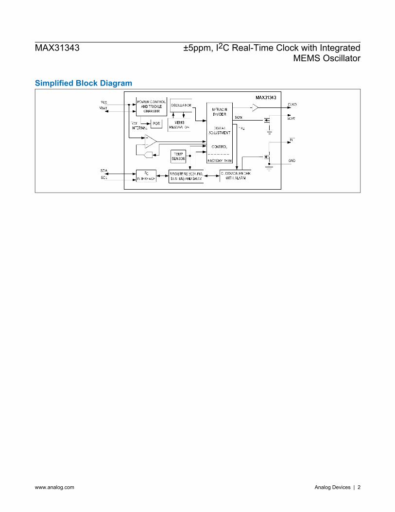
Simplified Block Diagram
I2C INTERFACE
REGISTE RS (CONFIG, STATUS) AND SRAM
CLOCK/CALENDAR WITH ALARM
TEMP SENSOR
N/FRAC-N DIVIDE R
DIGITA L ADJUSTMENT
CONTROL
FACTORY TRIM
INT
CLKO
SDA
SCL
POWER CONTROL AND TRICKLE
CHARGER
VCCVBAT
GND
MEMS RESONATOR
OSCILLATOR
MMAAXX3311334433
PORVCC INTERNA L 1Hz
SQW SQW
MAX31343 ±5ppm, I2C Real-Time Clock with IntegratedMEMS Oscillator
www.analog.com Analog Devices | 2
TABLE OF CONTENTS General Description . . . . . . . . . . . . . . . . . . . . . . . . . . . . . . . . . . . . . . . . . . . . . . . . . . . . . . . . . . . . . . . . . . . . . . . . . . . . . . 1 Applications . . . . . . . . . . . . . . . . . . . . . . . . . . . . . . . . . . . . . . . . . . . . . . . . . . . . . . . . . . . . . . . . . . . . . . . . . . . . . . . . . . . . 1 Benefits and Features . . . . . . . . . . . . . . . . . . . . . . . . . . . . . . . . . . . . . . . . . . . . . . . . . . . . . . . . . . . . . . . . . . . . . . . . . . . . 1 Simplified Block Diagram . . . . . . . . . . . . . . . . . . . . . . . . . . . . . . . . . . . . . . . . . . . . . . . . . . . . . . . . . . . . . . . . . . . . . . . . . 2 Absolute Maximum Ratings . . . . . . . . . . . . . . . . . . . . . . . . . . . . . . . . . . . . . . . . . . . . . . . . . . . . . . . . . . . . . . . . . . . . . . . . 7 Package Information . . . . . . . . . . . . . . . . . . . . . . . . . . . . . . . . . . . . . . . . . . . . . . . . . . . . . . . . . . . . . . . . . . . . . . . . . . . . . 7
8 WLP . . . . . . . . . . . . . . . . . . . . . . . . . . . . . . . . . . . . . . . . . . . . . . . . . . . . . . . . . . . . . . . . . . . . . . . . . . . . . . . . . . . . . . 7 8 TDFN . . . . . . . . . . . . . . . . . . . . . . . . . . . . . . . . . . . . . . . . . . . . . . . . . . . . . . . . . . . . . . . . . . . . . . . . . . . . . . . . . . . . . 7
Electrical Characteristics . . . . . . . . . . . . . . . . . . . . . . . . . . . . . . . . . . . . . . . . . . . . . . . . . . . . . . . . . . . . . . . . . . . . . . . . . 8 Typical Operating Characteristics . . . . . . . . . . . . . . . . . . . . . . . . . . . . . . . . . . . . . . . . . . . . . . . . . . . . . . . . . . . . . . . . . 11 Pin Configurations . . . . . . . . . . . . . . . . . . . . . . . . . . . . . . . . . . . . . . . . . . . . . . . . . . . . . . . . . . . . . . . . . . . . . . . . . . . . . . 12
8 WLP . . . . . . . . . . . . . . . . . . . . . . . . . . . . . . . . . . . . . . . . . . . . . . . . . . . . . . . . . . . . . . . . . . . . . . . . . . . . . . . . . . . . . 12 8 TDFN . . . . . . . . . . . . . . . . . . . . . . . . . . . . . . . . . . . . . . . . . . . . . . . . . . . . . . . . . . . . . . . . . . . . . . . . . . . . . . . . . . . . 12
Pin Description . . . . . . . . . . . . . . . . . . . . . . . . . . . . . . . . . . . . . . . . . . . . . . . . . . . . . . . . . . . . . . . . . . . . . . . . . . . . . . . . 13 Functional Block Diagram . . . . . . . . . . . . . . . . . . . . . . . . . . . . . . . . . . . . . . . . . . . . . . . . . . . . . . . . . . . . . . . . . . . . . . . . 13 Detailed Description . . . . . . . . . . . . . . . . . . . . . . . . . . . . . . . . . . . . . . . . . . . . . . . . . . . . . . . . . . . . . . . . . . . . . . . . . . . . 14
High-Accuracy Time Base . . . . . . . . . . . . . . . . . . . . . . . . . . . . . . . . . . . . . . . . . . . . . . . . . . . . . . . . . . . . . . . . . . . . . 14 Supply Operation . . . . . . . . . . . . . . . . . . . . . . . . . . . . . . . . . . . . . . . . . . . . . . . . . . . . . . . . . . . . . . . . . . . . . . . . . . . . 14 Power-Fail Interrupt Output . . . . . . . . . . . . . . . . . . . . . . . . . . . . . . . . . . . . . . . . . . . . . . . . . . . . . . . . . . . . . . . . . . . . 14 Real-Time Clock (RTC) . . . . . . . . . . . . . . . . . . . . . . . . . . . . . . . . . . . . . . . . . . . . . . . . . . . . . . . . . . . . . . . . . . . . . . . 14 Address Map . . . . . . . . . . . . . . . . . . . . . . . . . . . . . . . . . . . . . . . . . . . . . . . . . . . . . . . . . . . . . . . . . . . . . . . . . . . . . . . 15 RTC, Alarm, and Timer Registers . . . . . . . . . . . . . . . . . . . . . . . . . . . . . . . . . . . . . . . . . . . . . . . . . . . . . . . . . . . . . . . 15 Clock and Calendar . . . . . . . . . . . . . . . . . . . . . . . . . . . . . . . . . . . . . . . . . . . . . . . . . . . . . . . . . . . . . . . . . . . . . . . . . . 16 Alarms . . . . . . . . . . . . . . . . . . . . . . . . . . . . . . . . . . . . . . . . . . . . . . . . . . . . . . . . . . . . . . . . . . . . . . . . . . . . . . . . . . . . 16 Power Management . . . . . . . . . . . . . . . . . . . . . . . . . . . . . . . . . . . . . . . . . . . . . . . . . . . . . . . . . . . . . . . . . . . . . . . . . . 17 Trickle Charger . . . . . . . . . . . . . . . . . . . . . . . . . . . . . . . . . . . . . . . . . . . . . . . . . . . . . . . . . . . . . . . . . . . . . . . . . . . . . . 18 Temperature Sensor . . . . . . . . . . . . . . . . . . . . . . . . . . . . . . . . . . . . . . . . . . . . . . . . . . . . . . . . . . . . . . . . . . . . . . . . . 18 Interrupts Status and Output . . . . . . . . . . . . . . . . . . . . . . . . . . . . . . . . . . . . . . . . . . . . . . . . . . . . . . . . . . . . . . . . . . . 18 Data-Retention Mode . . . . . . . . . . . . . . . . . . . . . . . . . . . . . . . . . . . . . . . . . . . . . . . . . . . . . . . . . . . . . . . . . . . . . . . . . 18 Countdown Timer . . . . . . . . . . . . . . . . . . . . . . . . . . . . . . . . . . . . . . . . . . . . . . . . . . . . . . . . . . . . . . . . . . . . . . . . . . . . 19 Timing Diagram . . . . . . . . . . . . . . . . . . . . . . . . . . . . . . . . . . . . . . . . . . . . . . . . . . . . . . . . . . . . . . . . . . . . . . . . . . . . . 19 I2C Serial Port Operation . . . . . . . . . . . . . . . . . . . . . . . . . . . . . . . . . . . . . . . . . . . . . . . . . . . . . . . . . . . . . . . . . . . . . . 20 I2C Slave Address . . . . . . . . . . . . . . . . . . . . . . . . . . . . . . . . . . . . . . . . . . . . . . . . . . . . . . . . . . . . . . . . . . . . . . . . . . . 20 I2C Definitions . . . . . . . . . . . . . . . . . . . . . . . . . . . . . . . . . . . . . . . . . . . . . . . . . . . . . . . . . . . . . . . . . . . . . . . . . . . . . . 20 I2C Communication . . . . . . . . . . . . . . . . . . . . . . . . . . . . . . . . . . . . . . . . . . . . . . . . . . . . . . . . . . . . . . . . . . . . . . . . . . 22
Register Map . . . . . . . . . . . . . . . . . . . . . . . . . . . . . . . . . . . . . . . . . . . . . . . . . . . . . . . . . . . . . . . . . . . . . . . . . . . . . . . . . . 23 RC18 Register Map . . . . . . . . . . . . . . . . . . . . . . . . . . . . . . . . . . . . . . . . . . . . . . . . . . . . . . . . . . . . . . . . . . . . . . . . . . 23 Register Details . . . . . . . . . . . . . . . . . . . . . . . . . . . . . . . . . . . . . . . . . . . . . . . . . . . . . . . . . . . . . . . . . . . . . . . . . . . . . 25
Applications Information . . . . . . . . . . . . . . . . . . . . . . . . . . . . . . . . . . . . . . . . . . . . . . . . . . . . . . . . . . . . . . . . . . . . . . . . . 39
MAX31343 ±5ppm, I2C Real-Time Clock with IntegratedMEMS Oscillator
www.analog.com Analog Devices | 3

TABLE OF CONTENTS (CONTINUED) Power-Supply Decoupling . . . . . . . . . . . . . . . . . . . . . . . . . . . . . . . . . . . . . . . . . . . . . . . . . . . . . . . . . . . . . . . . . . . . . 39 Using Open-Drain Outputs . . . . . . . . . . . . . . . . . . . . . . . . . . . . . . . . . . . . . . . . . . . . . . . . . . . . . . . . . . . . . . . . . . . . . 39 SDA and SCL Pullup Resistors . . . . . . . . . . . . . . . . . . . . . . . . . . . . . . . . . . . . . . . . . . . . . . . . . . . . . . . . . . . . . . . . . 39 Handling . . . . . . . . . . . . . . . . . . . . . . . . . . . . . . . . . . . . . . . . . . . . . . . . . . . . . . . . . . . . . . . . . . . . . . . . . . . . . . . . . . . 39
Typical Application Circuit . . . . . . . . . . . . . . . . . . . . . . . . . . . . . . . . . . . . . . . . . . . . . . . . . . . . . . . . . . . . . . . . . . . . . . . . 39 Ordering Information . . . . . . . . . . . . . . . . . . . . . . . . . . . . . . . . . . . . . . . . . . . . . . . . . . . . . . . . . . . . . . . . . . . . . . . . . . . . 39 Revision History . . . . . . . . . . . . . . . . . . . . . . . . . . . . . . . . . . . . . . . . . . . . . . . . . . . . . . . . . . . . . . . . . . . . . . . . . . . . . . . 40
MAX31343 ±5ppm, I2C Real-Time Clock with IntegratedMEMS Oscillator
www.analog.com Analog Devices | 4

LIST OF FIGURES Figure 1. Trickle Charger Block Diagram . . . . . . . . . . . . . . . . . . . . . . . . . . . . . . . . . . . . . . . . . . . . . . . . . . . . . . . . . . . . 18 Figure 2. I2C Timing . . . . . . . . . . . . . . . . . . . . . . . . . . . . . . . . . . . . . . . . . . . . . . . . . . . . . . . . . . . . . . . . . . . . . . . . . . . . 19 Figure 3. I2C Slave Address . . . . . . . . . . . . . . . . . . . . . . . . . . . . . . . . . . . . . . . . . . . . . . . . . . . . . . . . . . . . . . . . . . . . . . 20 Figure 4. I2C Transactions . . . . . . . . . . . . . . . . . . . . . . . . . . . . . . . . . . . . . . . . . . . . . . . . . . . . . . . . . . . . . . . . . . . . . . . 22
MAX31343 ±5ppm, I2C Real-Time Clock with IntegratedMEMS Oscillator
www.analog.com Analog Devices | 5
LIST OF TABLES Table 1. Status and Configuration Registers . . . . . . . . . . . . . . . . . . . . . . . . . . . . . . . . . . . . . . . . . . . . . . . . . . . . . . . . . . 15 Table 2. RTC, Alarm, and Timer Registers . . . . . . . . . . . . . . . . . . . . . . . . . . . . . . . . . . . . . . . . . . . . . . . . . . . . . . . . . . . 15 Table 3. Alarm1 Register Mask Bits . . . . . . . . . . . . . . . . . . . . . . . . . . . . . . . . . . . . . . . . . . . . . . . . . . . . . . . . . . . . . . . . 16 Table 4. Alarm2 Register Mask Bits . . . . . . . . . . . . . . . . . . . . . . . . . . . . . . . . . . . . . . . . . . . . . . . . . . . . . . . . . . . . . . . . 16 Table 5. Power Management . . . . . . . . . . . . . . . . . . . . . . . . . . . . . . . . . . . . . . . . . . . . . . . . . . . . . . . . . . . . . . . . . . . . . 17 Table 6. Countdown Timer Setting . . . . . . . . . . . . . . . . . . . . . . . . . . . . . . . . . . . . . . . . . . . . . . . . . . . . . . . . . . . . . . . . . 19
MAX31343 ±5ppm, I2C Real-Time Clock with IntegratedMEMS Oscillator
www.analog.com Analog Devices | 6

Absolute Maximum Ratings Voltage Range on Any Pin Relative to GND ......... -0.3V to +6.0V Operating Temperature Range ............................ -40°C to +85°C Storage Temperature Range .............................. -55°C to +125°C
Junction Temperature .......................................................+150°C Lead Temperature (soldering, 10s) ...................................+300°C Soldering Temperature (reflow) ........................................+260°C
Stresses beyond those listed under “Absolute Maximum Ratings” may cause permanent damage to the device. These are stress ratings only, and functional operation of the device at these or any other conditions beyond those indicated in the operational sections of the specifications is not implied. Exposure to absolute maximum rating conditions for extended periods may affect device reliability.
Package Information
8 WLP Package Code K82A2+1 Outline Number 21-100336 Land Pattern Number N/A Thermal Resistance, Four-Layer Board: Junction to Ambient (θJA) 109.1°C/W Junction to Case (θJC) N/A
8 TDFN Package Code T834MKY+1 Outline Number 21-100322 Land Pattern Number 90-100121 Thermal Resistance, Four-Layer Board: Junction to Ambient (θJA) 47.44°C/W Junction to Case (θJC) 2.65°C/W
For the latest package outline information and land patterns (footprints), go to www.maximintegrated.com/packages. Note that a “+”, “#”, or “-” in the package code indicates RoHS status only. Package drawings may show a different suffix character, but the drawing pertains to the package regardless of RoHS status. Package thermal resistances were obtained using the method described in JEDEC specification JESD51-7, using a four-layer board. For detailed information on package thermal considerations, refer to www.maximintegrated.com/thermal-tutorial.
MAX31343 ±5ppm, I2C Real-Time Clock with IntegratedMEMS Oscillator
www.analog.com Analog Devices | 7
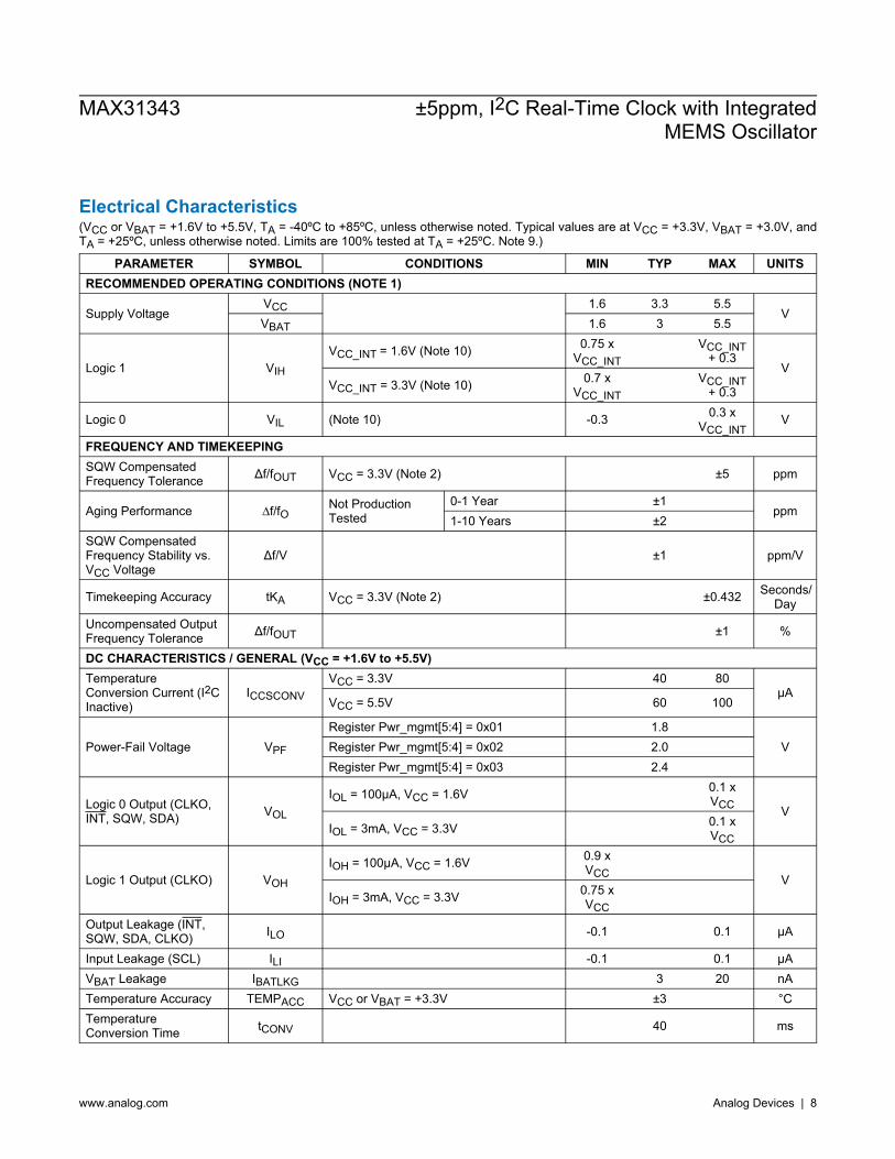
Electrical Characteristics (VCC or VBAT = +1.6V to +5.5V, TA = -40ºC to +85ºC, unless otherwise noted. Typical values are at VCC = +3.3V, VBAT = +3.0V, and TA = +25ºC, unless otherwise noted. Limits are 100% tested at TA = +25ºC. Note 9.)
PARAMETER SYMBOL CONDITIONS MIN TYP MAX UNITS RECOMMENDED OPERATING CONDITIONS (NOTE 1)
Supply Voltage VCC 1.6 3.3 5.5
V VBAT 1.6 3 5.5
Logic 1 VIH
VCC_INT = 1.6V (Note 10) 0.75 x VCC_INT
VCC_INT + 0.3
V VCC_INT = 3.3V (Note 10) 0.7 x
VCC_INT VCC_INT
+ 0.3
Logic 0 VIL (Note 10) -0.3 0.3 x VCC_INT
V
FREQUENCY AND TIMEKEEPING SQW Compensated Frequency Tolerance Δf/fOUT VCC = 3.3V (Note 2) ±5 ppm
Aging Performance ∆f/fO Not Production Tested
0-1 Year ±1 ppm
1-10 Years ±2 SQW Compensated Frequency Stability vs. VCC Voltage
Δf/V ±1 ppm/V
Timekeeping Accuracy tKA VCC = 3.3V (Note 2) ±0.432 Seconds/Day
Uncompensated Output Frequency Tolerance Δf/fOUT ±1 %
DC CHARACTERISTICS / GENERAL (VCC = +1.6V to +5.5V) Temperature Conversion Current (I2C Inactive)
ICCSCONV VCC = 3.3V 40 80
µA VCC = 5.5V 60 100
Power-Fail Voltage VPF
Register Pwr_mgmt[5:4] = 0x01 1.8 V Register Pwr_mgmt[5:4] = 0x02 2.0
Register Pwr_mgmt[5:4] = 0x03 2.4
Logic 0 Output (CLKO, INT, SQW, SDA) VOL
IOL = 100µA, VCC = 1.6V 0.1 x VCC V
IOL = 3mA, VCC = 3.3V 0.1 x VCC
Logic 1 Output (CLKO) VOH
IOH = 100μA, VCC = 1.6V 0.9 x VCC V
IOH = 3mA, VCC = 3.3V 0.75 x VCC
Output Leakage (INT, SQW, SDA, CLKO) ILO -0.1 0.1 µA
Input Leakage (SCL) ILI -0.1 0.1 µA VBAT Leakage IBATLKG 3 20 nA Temperature Accuracy TEMPACC VCC or VBAT = +3.3V ±3 °C Temperature Conversion Time tCONV 40 ms
MAX31343 ±5ppm, I2C Real-Time Clock with IntegratedMEMS Oscillator
www.analog.com Analog Devices | 8
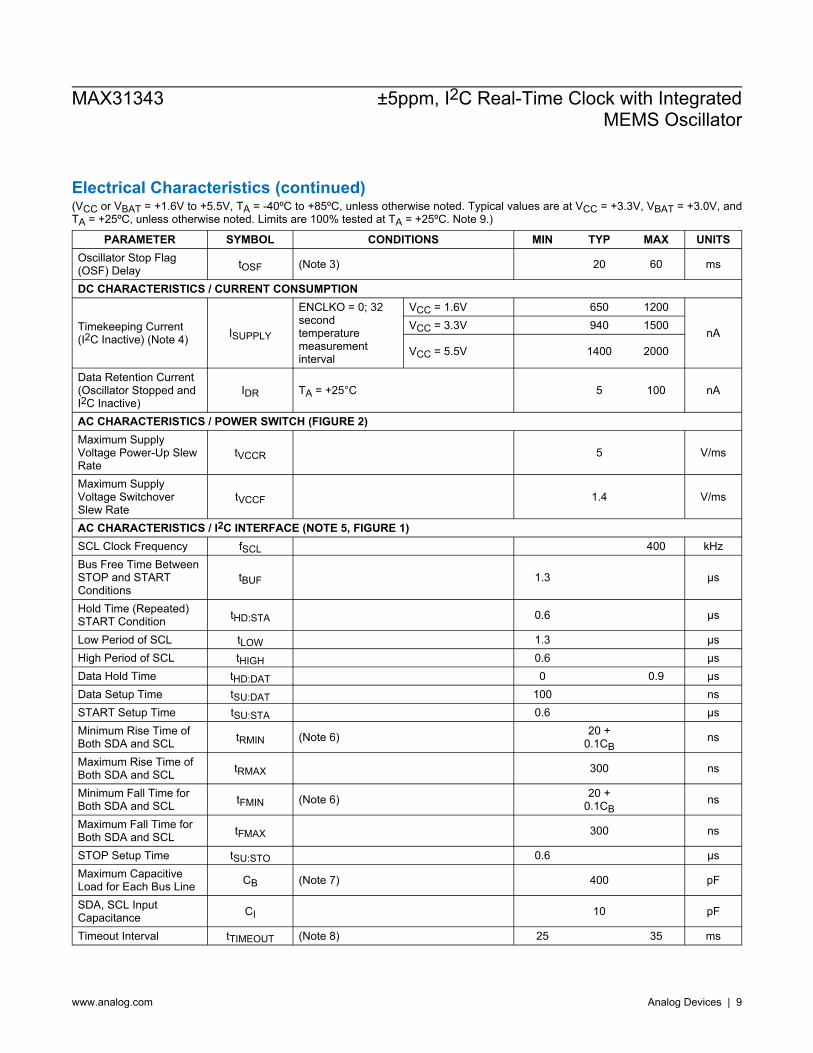
Electrical Characteristics (continued) (VCC or VBAT = +1.6V to +5.5V, TA = -40ºC to +85ºC, unless otherwise noted. Typical values are at VCC = +3.3V, VBAT = +3.0V, and TA = +25ºC, unless otherwise noted. Limits are 100% tested at TA = +25ºC. Note 9.)
PARAMETER SYMBOL CONDITIONS MIN TYP MAX UNITS Oscillator Stop Flag (OSF) Delay tOSF (Note 3) 20 60 ms
DC CHARACTERISTICS / CURRENT CONSUMPTION
Timekeeping Current (I2C Inactive) (Note 4) ISUPPLY
ENCLKO = 0; 32 second temperature measurement interval
VCC = 1.6V 650 1200
nA VCC = 3.3V 940 1500
VCC = 5.5V 1400 2000
Data Retention Current (Oscillator Stopped and I2C Inactive)
IDR TA = +25°C 5 100 nA
AC CHARACTERISTICS / POWER SWITCH (FIGURE 2) Maximum Supply Voltage Power-Up Slew Rate
tVCCR 5 V/ms
Maximum Supply Voltage Switchover Slew Rate
tVCCF 1.4 V/ms
AC CHARACTERISTICS / I2C INTERFACE (NOTE 5, FIGURE 1) SCL Clock Frequency fSCL 400 kHz Bus Free Time Between STOP and START Conditions
tBUF 1.3 μs
Hold Time (Repeated) START Condition tHD:STA 0.6 μs
Low Period of SCL tLOW 1.3 μs High Period of SCL tHIGH 0.6 μs Data Hold Time tHD:DAT 0 0.9 μs Data Setup Time tSU:DAT 100 ns START Setup Time tSU:STA 0.6 μs Minimum Rise Time of Both SDA and SCL tRMIN (Note 6) 20 +
0.1CB ns
Maximum Rise Time of Both SDA and SCL tRMAX 300 ns
Minimum Fall Time for Both SDA and SCL tFMIN (Note 6) 20 +
0.1CB ns
Maximum Fall Time for Both SDA and SCL tFMAX 300 ns
STOP Setup Time tSU:STO 0.6 μs Maximum Capacitive Load for Each Bus Line CB (Note 7) 400 pF
SDA, SCL Input Capacitance CI 10 pF
Timeout Interval tTIMEOUT (Note 8) 25 35 ms
MAX31343 ±5ppm, I2C Real-Time Clock with IntegratedMEMS Oscillator
www.analog.com Analog Devices | 9

Note 1: All voltages are referenced to ground. Note 2: Frequency accuracy is measured over 512s interval. Note 3: The parameter tOSF is the period of time the oscillator must be stopped for the OSF flag to be set. Note 4: Includes the temperature conversion current (averaged). Note 5: Interface timing shown is for fast-mode (400kHz) operation. This device is also backward-compatible with standard mode I2C
timing. Note 6: Guaranteed by design; not 100% production tested. Note 7: CB: Total capacitance of one bus line in picofarads. Note 8: The MAX31343 can detect any single SCL clock held low longer than tTIMEOUTMIN. The device I2C interface is in reset
state and can receive a new START condition when SCL is held low for at least tTIMEOUTMAX. Once the device detects this condition, the SDA output is released. The oscillator must be running for this function to work.
Note 9: Limits at -40ºC and +85ºC are guaranteed by design and characterization. Note 10: VCC_INT is the active internal supply. VCC_INT = VBAT when VCC < VPF and VCC < VBAT; VCC_INT = VCC in all other
conditions in Power Management Auto mode (see Table 5).
MAX31343 ±5ppm, I2C Real-Time Clock with IntegratedMEMS Oscillator
www.analog.com Analog Devices | 10
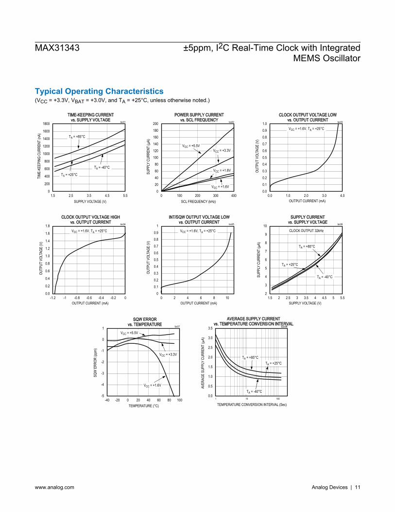
Typical Operating Characteristics (VCC = +3.3V, VBAT = +3.0V, and TA = +25°C, unless otherwise noted.)
MAX31343 ±5ppm, I2C Real-Time Clock with IntegratedMEMS Oscillator
www.analog.com Analog Devices | 11

Pin Configurations
8 WLP
A3 A2 A1
+
TOP VIEW
A4
VCCINTSQW CLKO
B3 B2 B1B4
SDAVBAT SCLGND
MAX31343MAX31343
8 TDFN
++
3mm x 4mm3mm x 4mm
TOP VIEW
8SCL
7SDA
6VBAT
5GND
4
SQW
3
INT
2
VCC
1
CLKO
MAX31343MAX31343
MAX31343 ±5ppm, I2C Real-Time Clock with IntegratedMEMS Oscillator
www.analog.com Analog Devices | 12
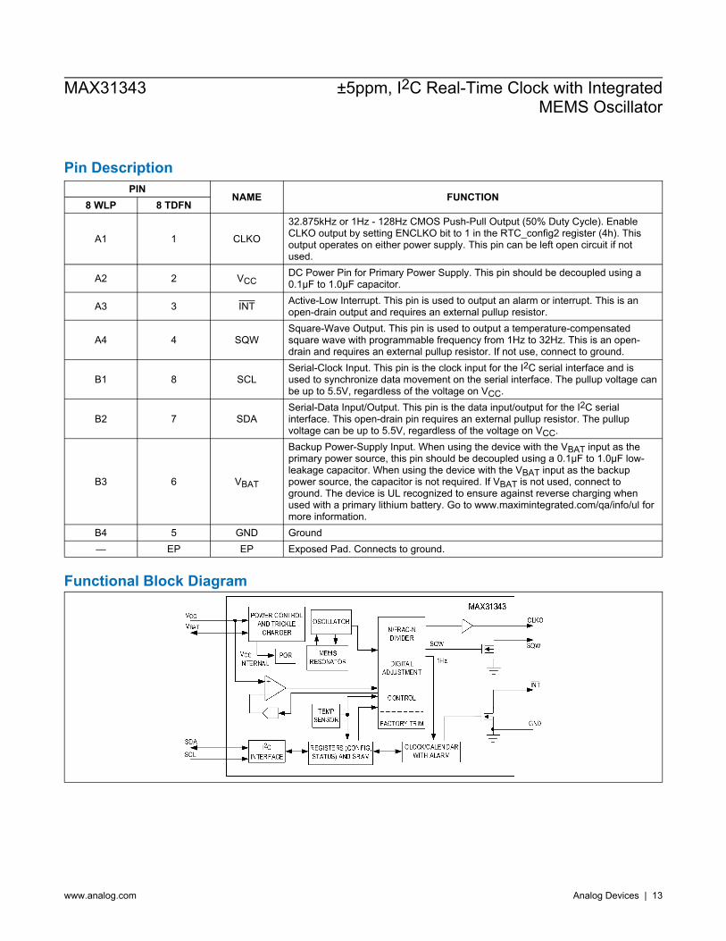
Pin Description PIN
NAME FUNCTION 8 WLP 8 TDFN
A1 1 CLKO
32.875kHz or 1Hz - 128Hz CMOS Push-Pull Output (50% Duty Cycle). Enable CLKO output by setting ENCLKO bit to 1 in the RTC_config2 register (4h). This output operates on either power supply. This pin can be left open circuit if not used.
A2 2 VCC DC Power Pin for Primary Power Supply. This pin should be decoupled using a 0.1μF to 1.0μF capacitor.
A3 3 INT Active-Low Interrupt. This pin is used to output an alarm or interrupt. This is an open-drain output and requires an external pullup resistor.
A4 4 SQW Square-Wave Output. This pin is used to output a temperature-compensated square wave with programmable frequency from 1Hz to 32Hz. This is an open-drain and requires an external pullup resistor. If not use, connect to ground.
B1 8 SCL Serial-Clock Input. This pin is the clock input for the I2C serial interface and is used to synchronize data movement on the serial interface. The pullup voltage can be up to 5.5V, regardless of the voltage on VCC.
B2 7 SDA Serial-Data Input/Output. This pin is the data input/output for the I2C serial interface. This open-drain pin requires an external pullup resistor. The pullup voltage can be up to 5.5V, regardless of the voltage on VCC.
B3 6 VBAT
Backup Power-Supply Input. When using the device with the VBAT input as the primary power source, this pin should be decoupled using a 0.1μF to 1.0μF low-leakage capacitor. When using the device with the VBAT input as the backup power source, the capacitor is not required. If VBAT is not used, connect to ground. The device is UL recognized to ensure against reverse charging when used with a primary lithium battery. Go to www.maximintegrated.com/qa/info/ul for more information.
B4 5 GND Ground — EP EP Exposed Pad. Connects to ground.
Functional Block Diagram
I2C INTERFACE
REGISTE RS (CONFIG, STATUS) AND SRAM
CLOCK/CALENDAR WITH ALARM
TEMP SENSOR
N/FRAC-N DIVIDE R
DIGITA L ADJUSTMENT
CONTROL
FACTORY TRIM
INT
CLKO
SDA
SCL
POWER CONTROL AND TRICKLE
CHARGER
VCCVBAT
GND
MEMS RESONATOR
OSCILLATOR
MMAAXX3311334433
PORVCC INTERNA L 1Hz
SQW SQW
MAX31343 ±5ppm, I2C Real-Time Clock with IntegratedMEMS Oscillator
www.analog.com Analog Devices | 13
Detailed Description The MAX31343 is a serial real-time clock (RTC) driven by an internal temperature-compensated microelectromechanical systems (MEMS) resonator. The oscillator provides a stable and accurate reference clock and maintains the RTC to within ±0.432 seconds-per-day accuracy from -40°C to +85°C. The RTC is a low-power clock/calendar with two programmable alarms. INT provides an interrupt signal due to alarm1 or alarm2 conditions. SQW outputs programmable temperature compensated square wave. Pin CLKO is an uncompensated output. The clock/calendar provides seconds, minutes, hours, day, date, month, year, and century information. The date at the end of the month is automatically adjusted for months with fewer than 31 days, including corrections for leap year up to year 2199. The clock operates in the 24-hour format. The internal registers are accessible though an I2C bus interface. An internal comparator circuit monitors the level of VCC to detect power failures and to automatically switch to the backup supply when necessary.
High-Accuracy Time Base The temperature sensor, oscillator, and digital adjustment controller logic form the highly accurate time base. The controller reads the output of the on-chip temperature sensor and adjusts the final compensated SQW output to maintain the required accuracy. The device is trimmed at the factory to maintain a tight accuracy over the operating temperature range. The device has options to manually set the rate of temperature compensation through TTSINT bits in register TS_config (0x1C), or allow the system to adjust the rate automatically. Aging is the change in the internally compensated oscillation frequency. Unlike most crystal-based RTCs, the MAX31343 has very good aging performance. It is less than ±1ppm for zero to one year, and less than ±2ppm for one to ten years.
Supply Operation There are several modes of operation that affect the amount of supply current that is drawn. While the serial interface is active, the active supply current is shown in the POWER SUPPLY CURRENT vs. SCL FREQUENCY plot. When the serial interface is inactive, the timekeeping current ISUPPLY (which includes the averaged temperature-conversion current) is used. The temperature-conversion current ICCSCONV is specified since the system must be able to support the periodic higher current pulse and still maintain a valid voltage level. The data-retention current IDR is the current drawn by the device when major internal blocks (including oscillator) are powered down except the I2C interface (DATA_RET = 1). This mode can be used to minimize current consumption when maintaining time and date information is not necessary (e.g., while the end system is waiting to be shipped to a customer).
Power-Fail Interrupt Output When VCC falls below VPF, an internal power-fail signal is generated, which forces INT low if power-fail interrupt is enabled.
Real-Time Clock (RTC) With the 1Hz source from the temperature-compensated oscillator, the RTC provides seconds, minutes, hours, day, date, month, year, and century information. The date at the end of the month is automatically adjusted for months with fewer than 31 days, including corrections for leap year up to year 2199. The clock operates in the 24-hour format. The clock provides two programmable time-of-day alarms. INT can be enabled to generate an interrupt due to any of alarm1, alarm2, timer, temperature sense or power-fail condition. The SQW output generates a temperature-compensated square wave.
MAX31343 ±5ppm, I2C Real-Time Clock with IntegratedMEMS Oscillator
www.analog.com Analog Devices | 14

Address Map Table 1 shows the Status register and various RTC configuration registers. The Interrupt Enable (Int_en) register contains an enable bit for each of the interrupt bits. Disable Oscillator Flag (DOSF) is used to enable or disable the indication of the oscillator status through OSF flag. When an interrupt occurs, if the corresponding enable bit for that type of interrupt has been asserted, the corresponding bit in the Status register bit will be set. A read of the Status register will clear any of the flags that were set by interrupts.
Table 1. Status and Configuration Registers ADDR NAME B7 B6 B5 B4 B3 B2 B1 B0 0x00 Status PSDECT OSF PFAIL TSF TIF A2F A1F 0x01 Int_en DOSF PFAILE TSIE TIE A2IE A1IE 0x02 RTC_reset SWRST 0x03 RTC_config1 DATARET I2C_TIMEOUT ENOSC RESERVED 0x04 RTC_config2 ENCLKO CLKO_HZ[3:0] SQW_HZ[2:0] 0x05 Timer_config TE TPAUSE TRPT TFS[1:0]
RTC, Alarm, and Timer Registers Table 2 shows the address map for the device's RTC, alarm, and timer registers. During a multibyte access, when the address pointer reaches the end of the register space (5Dh), it wraps around to location 00h. On an I2C START or address pointer incrementing to location 06h, the current time is transferred to a second set of registers. The time information is read from these secondary registers, while the clock can continue to run. This eliminates the need to reread the registers in case the main registers update during a read.
Table 2. RTC, Alarm, and Timer Registers ADDR NAME B7 B6 B5 B4 B3 B2 B1 B0
0x06 Seconds sec_10[2:0] seconds[3:0] 0x07 Minutes min_10[2:0] minutes[3:0] 0x08 Hours hr_10[1:0] hour[3:0] 0x09 Day day[2:0] 0x0A Date date_10[1:0] date[3:0] 0x0B Month century month_10 month[3:0] 0x0C Year year_10[3:0] year[3:0] 0x0D Alm1_sec A1M1 sec_10[2:0] seconds[3:0] 0x0E Alm1_min A1M2 min_10[2:0] minutes[3:0] 0x0F Alm1_hrs A1M3 hr_10[1:0] hour[3:0] 0x10 Alm1day_date A1M4 DY_DT date_10[1:0] day_date[3:0] 0x11 Alm1_mon A1M5 A1M6 month_10 month[3:0] 0x12 Alm1_year year_10[3:0] year[3:0] 0x13 Alm2_min A2M2 min_10[2:0] minutes[3:0] 0x14 Alm2_hrs A2M3 hr_10[1:0] hour[3:0] 0x15 Alm2day_date A2M4 DY_DT date_10[1:0] day_date[3:0] 0x16 Timer_count count[7:0] 0x17 Time_init count[7:0]
MAX31343 ±5ppm, I2C Real-Time Clock with IntegratedMEMS Oscillator
www.analog.com Analog Devices | 15

Clock and Calendar The time and calendar information is obtained by reading the appropriate register bytes. Table 2 shows the RTC registers. The time and calendar data are set or initialized by writing the appropriate register bytes. Time will be updated 1 second after user sets the timer registers. The contents of the time and calendar registers are in the binary-coded decimal (BCD) format. The device runs in 24-hour mode. The century bit (bit 7 of the Month register) is toggled when the Years register overflows from 99 to 00. The day-of-week register increments at midnight. Values that correspond to the day of week are user-defined but must be sequential (i.e., if 1 equals Sunday, then 2 equals Monday, and so on). Illogical time and date entries result in undefined operation. When reading or writing the time and date registers, secondary buffers are used to prevent errors when the internal registers update. When reading the time and date registers, the secondary buffers are synchronized to the internal registers on any I2C START and when the register pointer rolls over to zero. The time information is read from these secondary registers, while the clock continues to run. This eliminates the need to reread the registers in case the main registers update during a read.
Alarms The device contains two time-of-day/date alarms. Alarm 1 can be set by writing to registers 0Dh–12h. Alarm 2 can be set by writing to registers 13h–15h. See Table 3 and Table 4. The alarms can be programmed by the A1IE and A2IE bits in Int_en register to activate the INT output on an alarm match condition. Bit 7 of each of the time-of-day/date alarm registers and bit 6 of Alm1_mon register are mask bits (Table 3). When all the mask bits for each alarm are logic 0, an alarm only occurs when the values in the timekeeping registers match the corresponding values stored in the time-of-day, date, month, and year alarm registers. The alarms can also be programmed to repeat every second, minute, hour, day, or date. Table 3 and Table 4 show the possible settings. Configurations not listed in the table result in illogical operation. The DY_DT bit (bit 6 of the alarm day/date registers) controls whether the alarm value stored in bits 0–5 of that register represents the day of the week or the date of the month. If DY_DT is written to logic 0, the alarm is the result of a match with date of the month. If DY_DT is written to logic 1, the alarm is the result of a match with day of the week. Disable alarms before programming alarm registers, then enable them 1 second after alarm configured.
Table 3. Alarm1 Register Mask Bits DY/DT ALARM 1 REGISTER MASK BITS ALARM RATE
A1M6 A1M5 A1M4 A1M3 A1M2 A1M1 X 1 1 1 1 1 1 Alarm once a second X 1 1 1 1 1 0 Alarm when seconds match X 1 1 1 1 0 0 Alarm when minutes and seconds match X 1 1 1 0 0 0 Alarm when hours, minutes, and seconds match 0 1 1 0 0 0 0 Alarm when dates, hours, minutes, and seconds match 0 1 0 0 0 0 0 Alarm when months, dates, hours, minutes, and seconds match 0 0 0 0 0 0 0 Alarm when years, months, dates, hours, minutes, and seconds match 1 1 1 0 0 0 0 Alarm when days, hours, minutes, and seconds match
Table 4. Alarm2 Register Mask Bits DY/DT ALARM 2 REGISTER MASK BITS ALARM RATE
A2M4 A2M3 A2M2 Alarm once per minute (00 seconds of every minute) X 1 1 1 Alarm when minutes match X 1 1 0 Alarm when hours and minutes match X 1 0 0 Alarm when dates, hours, and minutes match 0 0 0 0 Alarm when days, hours, and minutes match 1 0 0 0 Alarm when days, hours, and minutes match
MAX31343 ±5ppm, I2C Real-Time Clock with IntegratedMEMS Oscillator
www.analog.com Analog Devices | 16
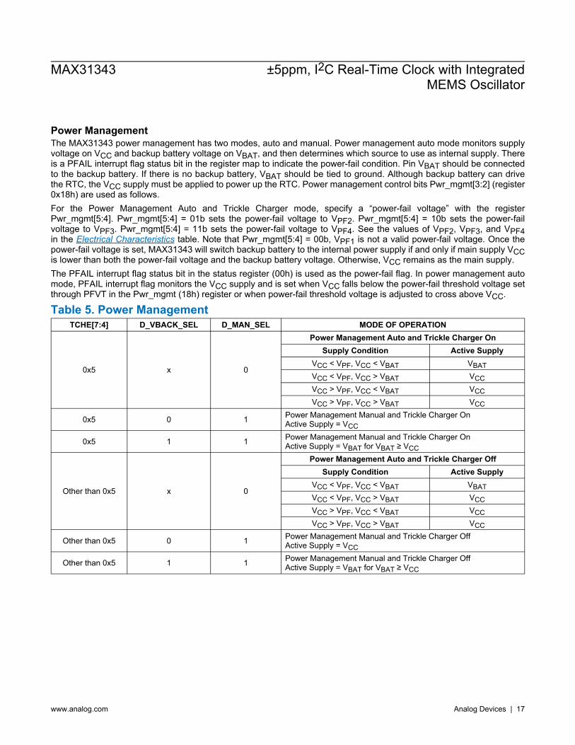
Power Management The MAX31343 power management has two modes, auto and manual. Power management auto mode monitors supply voltage on VCC and backup battery voltage on VBAT, and then determines which source to use as internal supply. There is a PFAIL interrupt flag status bit in the register map to indicate the power-fail condition. Pin VBAT should be connected to the backup battery. If there is no backup battery, VBAT should be tied to ground. Although backup battery can drive the RTC, the VCC supply must be applied to power up the RTC. Power management control bits Pwr_mgmt[3:2] (register 0x18h) are used as follows. For the Power Management Auto and Trickle Charger mode, specify a “power-fail voltage” with the register Pwr_mgmt[5:4]. Pwr_mgmt[5:4] = 01b sets the power-fail voltage to VPF2. Pwr_mgmt[5:4] = 10b sets the power-fail voltage to VPF3. Pwr_mgmt[5:4] = 11b sets the power-fail voltage to VPF4. See the values of VPF2, VPF3, and VPF4 in the Electrical Characteristics table. Note that Pwr_mgmt[5:4] = 00b, VPF1 is not a valid power-fail voltage. Once the power-fail voltage is set, MAX31343 will switch backup battery to the internal power supply if and only if main supply VCC is lower than both the power-fail voltage and the backup battery voltage. Otherwise, VCC remains as the main supply. The PFAIL interrupt flag status bit in the status register (00h) is used as the power-fail flag. In power management auto mode, PFAIL interrupt flag monitors the VCC supply and is set when VCC falls below the power-fail threshold voltage set through PFVT in the Pwr_mgmt (18h) register or when power-fail threshold voltage is adjusted to cross above VCC.
Table 5. Power Management TCHE[7:4] D_VBACK_SEL D_MAN_SEL MODE OF OPERATION
0x5 x 0
Power Management Auto and Trickle Charger On Supply Condition Active Supply
VCC < VPF, VCC < VBAT VBAT VCC < VPF, VCC > VBAT VCC VCC > VPF, VCC < VBAT VCC VCC > VPF, VCC > VBAT VCC
0x5 0 1 Power Management Manual and Trickle Charger On Active Supply = VCC
0x5 1 1 Power Management Manual and Trickle Charger On Active Supply = VBAT for VBAT ≥ VCC
Other than 0x5 x 0
Power Management Auto and Trickle Charger Off Supply Condition Active Supply
VCC < VPF, VCC < VBAT VBAT VCC < VPF, VCC > VBAT VCC VCC > VPF, VCC < VBAT VCC VCC > VPF, VCC > VBAT VCC
Other than 0x5 0 1 Power Management Manual and Trickle Charger Off Active Supply = VCC
Other than 0x5 1 1 Power Management Manual and Trickle Charger Off Active Supply = VBAT for VBAT ≥ VCC
MAX31343 ±5ppm, I2C Real-Time Clock with IntegratedMEMS Oscillator
www.analog.com Analog Devices | 17
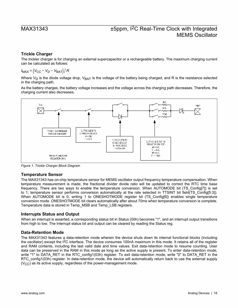
Trickle Charger The trickler charger is for charging an external supercapacitor or a rechargeable battery. The maximum charging current can be calculated as follows:
IMAX = (VCC − VD − VBAT) / R Where VD is the diode voltage drop, VBAT is the voltage of the battery being charged, and R is the resistance selected in the charging path. As the battery charges, the battery voltage increases and the voltage across the charging path decreases. Therefore, the charging current also decreases.
3kΩ
6kΩ
11kΩ
TCHE = 0x5 ENABLESTRICKLE CHA RGER
D_TRICKLE BIT2DIODE SE LECT0 = W/O DIODE1 = W DIODE
D_TRICKLE BITS[1 :0]RESISTOR SELECT
00 = 3kΩ 01 = 3kΩ10 = 6kΩ
11 = 11kΩ
D_TRICKLE BIT3CHARGER SE LECT
0 = ON1 = OFF
TRICKLE CHA RGER REGISTE R (19H)
VCC VBAT
Figure 1. Trickle Charger Block Diagram
Temperature Sensor The MAX31343 has on-chip temperature sensor for MEMS oscillator output frequency temperature compensation. When temperature measurement is made, the fractional divider divide ratio will be updated to correct the RTC time base frequency. There are two ways to enable the temperature conversion. When AUTOMODE bit (TS_Config[7]) is set to 1, temperature sensor performs conversion automatically at the rate selected in TTSINT bit field(TS_Config[5:3]). When AUTOMODE bit is 0, writing 1 to ONESHOTMODE register bit (TS_Config[6]) enables single temperature conversion mode. ONESHOTMODE bit clears automatically after about 70ms when temperature conversion is complete. Temperature data is stored in Temp_MSB and Temp_LSB registers.
Interrupts Status and Output When an interrupt is asserted, a corresponding status bit in Status (00h) becomes "1", and an interrupt output transitions from high to low. The Interrupt status bit and output can be cleared by reading the Status reg.
Data-Retention Mode The MAX31343 features a data-retention mode wherein the device shuts down its internal functional blocks (including the oscillator) except the I2C interface. The device consumes 100nA maximum in this mode. It retains all of the register and RAM contents, including the last valid date and time values. Exit data-retention mode to resume counting. User data can be preserved in the RAM in this mode as long as the active supply is present. To enter data-retention mode, write "1" to DATA_RET in the RTC_config1(03h) register. To exit data-retention mode, write "0" to DATA_RET in the RTC_config1(03h) register. In data-retention mode, the device will automatically return back to use the external supply (VCC) as its active supply, regardless of the power-management mode.
MAX31343 ±5ppm, I2C Real-Time Clock with IntegratedMEMS Oscillator
www.analog.com Analog Devices | 18
Countdown Timer The MAX31343 features a countdown timer with a pause function. The timer can be configured by writing into registers Timer_config (05h) and Timer_init (17h). The Timer_init register should be loaded with the initial value from which the timer would start counting down. The Timer_config register allows these configuration options: ● Select the frequency of the timer using the TFS[1:0] field. ● Start/stop the timer using the TE (Timer Enable) bit. ● Enable/disable the timer repeat function using the TRPT bit. This function reloads and restarts the timer with the
same init value once it counts down to zero. ● Pause/resume the countdown at any time when the timer is enabled using the TPAUSE bit (explained below). The timer can be programmed to assert the INT output (see Table 6) whenever it counts down to zero. This can be enabled/disabled using the TIE bit in register Int_en register (01h). The TPAUSE bit is only valid when TE = 1. This bit must be reset to 0 whenever TE is reset to 0. Table 6 highlights the steps to be used for various use cases involving TE and TPAUSE. Typical use cases: ● Countdown timer without pause: Step 1 -> Step 2 -> Step 1 and so on ● Countdown timer with pause: Step 1 -> Step 2 -> Step 3a -> Step 3b -> Step 1 and so on
Table 6. Countdown Timer Setting SEQUENCE TE TPAUSE ACTION
Step 1 0 0 Countdown timer is reset, and ready for next countdown operation. Timer_init can be programmed in this state.
Step 2 1 0 Countdown timer starts counting down from the value programmed in Timer_init Step 3a
(Optional) 1 1 Countdown timer is paused, and is ready to start counting down when TPAUSE is programmed back to ‘0’. Contents of the countdown timer are preserved in this state.
Step 3b If 3a is true 1 0 Countdown timer is brought out of pause state, and starts counting down from the paused value.
0 1 Not allowed
Timing Diagram
SCL
NOTE:NOTE: TIMING IS REFERENCED TO VILMAX AND VIHMIN.
SDA
STOP START REPEATEDSTART
tBUF
tHD:STA
tHD:DAT tSU:DAT
tSU:STO
tHD:STAtSP
tSU:STAtHIGH
tR
tFtLOW
Figure 2. I2C Timing
MAX31343 ±5ppm, I2C Real-Time Clock with IntegratedMEMS Oscillator
www.analog.com Analog Devices | 19
I2C Serial Port Operation
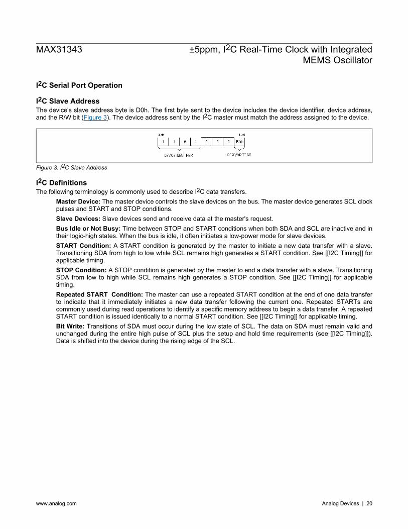
I2C Slave Address The device's slave address byte is D0h. The first byte sent to the device includes the device identifier, device address, and the R/W bit (Figure 3). The device address sent by the I2C master must match the address assigned to the device.
R/W
Figure 3. I2C Slave Address
I2C Definitions The following terminology is commonly used to describe I2C data transfers.
Master Device: The master device controls the slave devices on the bus. The master device generates SCL clock pulses and START and STOP conditions. Slave Devices: Slave devices send and receive data at the master's request. Bus Idle or Not Busy: Time between STOP and START conditions when both SDA and SCL are inactive and in their logic-high states. When the bus is idle, it often initiates a low-power mode for slave devices. START Condition: A START condition is generated by the master to initiate a new data transfer with a slave. Transitioning SDA from high to low while SCL remains high generates a START condition. See [[I2C Timing]] for applicable timing. STOP Condition: A STOP condition is generated by the master to end a data transfer with a slave. Transitioning SDA from low to high while SCL remains high generates a STOP condition. See [[I2C Timing]] for applicable timing. Repeated START Condition: The master can use a repeated START condition at the end of one data transfer to indicate that it immediately initiates a new data transfer following the current one. Repeated STARTs are commonly used during read operations to identify a specific memory address to begin a data transfer. A repeated START condition is issued identically to a normal START condition. See [[I2C Timing]] for applicable timing. Bit Write: Transitions of SDA must occur during the low state of SCL. The data on SDA must remain valid and unchanged during the entire high pulse of SCL plus the setup and hold time requirements (see [[I2C Timing]]). Data is shifted into the device during the rising edge of the SCL.
MAX31343 ±5ppm, I2C Real-Time Clock with IntegratedMEMS Oscillator
www.analog.com Analog Devices | 20

Bit Read: At the end of a write operation, the master must release the SDA bus line for the proper amount of setup time (see [[I2C Timing]]) before the next rising edge of SCL during a bit read. The device shifts out each bit of data on SDA at the falling edge of the previous SCL pulse and the data bit is valid at the rising edge of the current SCL pulse. Remember that the master generates all SCL clock pulses including when it is reading bits from the slave. Acknowledge (ACK and NACK): An acknowledge (ACK) or not acknowledge (NACK) is always the ninth bit transmitted during a byte transfer. The device receiving data (the master during a read or the slave during a write operation) performs an ACK by trans- mitting a 0 during the ninth bit. A device performs a NACK by transmitting a 1 during the ninth bit. Timing for the ACK and NACK is identical to all other bit writes. An ACK is the acknowledgment that the device is properly receiving data. A NACK is used to terminate a read sequence or as an indication that the device is not receiving data. Byte Write: A byte write consists of 8 bits of information transferred from the master to the slave (most significant bit first) plus a 1-bit acknowledgment from the slave to the master. The 8 bits transmitted by the master are done according to the bit write definition and the acknowledgment is read using the bit read definition. Byte Read: A byte read is an 8-bit information transfer from the slave to the master plus a 1-bit ACK or NACK from the master to the slave. The 8 bits of information that are transferred (most significant bit first) from the slave to the master are read by the master using the bit read definition, and the master transmits an ACK using the bit write definition to receive additional data bytes. The master must NACK the last byte read to terminate communication so the slave returns control of SDA to the master. Slave Address Byte: Each slave on the I2C bus responds to a slave address byte sent immediately following a START condition. The slave address byte contains the slave address in the most significant 7 bits and the R/W bit in the least significant bit. The device's slave address is D0h and cannot be modified by the user. When the R/W bit is 0 (such as in D0h), the master is indicating it writes data to the slave. If R/W = 1 (D1h in this case), the master is indicating it wants to read from the slave. If an incorrect slave address is written, the device assumes the master is communicating with another I2C device and ignore the communication until the next START condition is sent. Memory Address: During an I2C write operation, the master must transmit a memory address to identify the memory location where the slave is to store the data. The memory address is always the second byte transmitted during a write operation following the slave address byte.
MAX31343 ±5ppm, I2C Real-Time Clock with IntegratedMEMS Oscillator
www.analog.com Analog Devices | 21

I2C Communication See Figure 4 for an I2C communication example.
SLAV E ADDRE SS
START
START
1 1 0 1 0 0 0 R/W SLAV E ACK
SLAV E ACK
SLAV E ACK STOP
MSB LSB MSB LSB MSB LSB
b7 b6 b5 b4 b3 b2 b1 b0
READ/WRITE REGISTE R ADDRESS
b7 b6 b5 b4 b3 b2 b1 b0
DATA
SINGLE BYTE W RITE-WRITE CONFIGURATION REGISTERTO 0Ah
MULTIBYTE WRITE-WRITE DATE REGISTERTO "02" AND MONTHREGISTE R TO "11"
SINGLE BYTE READ-READ CONFIGURATION REGIS TER
MULTIBYTE READ-READ ALARM 2 HOURSAND DATE VALUES
START SLAV E ACK
SLAV E ACK
REPEATED START
D1hSLAV E
ACKMAS TER
NACK STOP1 1 0 1 0 0 0 0 0 0 0 0 0 0 1 1
03h
1 1 0 1 0 0 0 1 VALUE
SLAV E ACK1 1 0 1 0 0 0 0 0 0 0 0 0 0 1 1
D0h 03h
STOP
START SLAV E ACK
SLAV E ACK1 1 0 1 0 0 0 0 0 0 0 0 1 0 1 0
D0h 0AhSLAV E
ACK
DATA
MAS TER NACK STOPVALUE
DATA
02h
0AhEXAMPLE I2C TRANS ACTIONS
TYPICAL I2C WRITE TRANSACTION
0 0 0 0 1 0 1 0
0 0 0 0 0 0 1 0
D0h
A)
C)
B)
D)
SLAV E ACK
SLAV E ACK
REPEATED START
D1hSLAV E
ACKMAS TER
ACK1 1 0 1 0 0 0 1 VALUE
DATA
START SLAV E ACK
SLAV E ACK1 1 0 1 0 0 0 0 0 0 0 1 0 1 0 0
D0h 14h
SLAV E ACK STOP
11h
0 0 0 1 0 0 0 1
Figure 4. I2C Transactions
Writing a Single Byte to a Slave: The master must generate a START condition, write the slave address byte (R/W = 0), write the memory address, write the byte of data, and generate a STOP condition. Remember the master must read the slave's acknowledgment during all byte write operations. Writing Multiple Bytes to a Slave: To write multiple bytes to a slave, the master generates a START con- dition, writes the slave address byte (R/W = 0), writes the starting memory address, writes multiple data bytes, and generates a STOP condition. Reading a Single Byte from a Slave: Unlike the write operation that uses the specified memory address byte to define where the data is to be written, the read operation occurs at the present value of the memory address counter. To read a single byte from the slave, the master generates a START condition, writes the slave address byte with R/W = 1, reads the data byte with a NACK to indicate the end of the transfer, and generates a STOP condition. However, since requiring the master to keep track of the memory address counter is impractical, use the method for manipulating the address counter for reads. Manipulating the Address Counter for Reads: A dummy write cycle can be used to force the address counter to a particular value. To do this the master generates a START condition, writes the slave address byte (R/W = 0), writes the memory address where it desires to read, generates a repeated START condition, writes the slave address byte (R/W = 1), reads data with ACK or NACK as applicable, and generates a STOP condition. See Figure 4 for a read example using the repeated START condition to specify the starting memory location. Reading Multiple Bytes from a Slave: The read operation can be used to read multiple bytes with a single transfer. When reading bytes from the slave, the master simply ACKs the data byte if it desires to read another byte before terminating the transaction. After the master reads the last byte it must NACK to indicate the end of the transfer and then it generates a STOP condition.
MAX31343 ±5ppm, I2C Real-Time Clock with IntegratedMEMS Oscillator
www.analog.com Analog Devices | 22
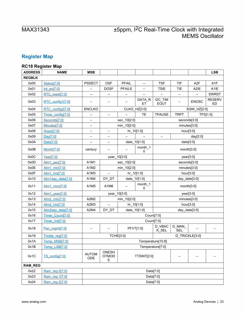
Register Map
RC18 Register Map ADDRESS NAME MSB LSB REGBLK
0x00 Status[7:0] PSDECT OSF PFAIL – TSF TIF A2F A1F 0x01 Int_en[7:0] – DOSF PFAILE – TSIE TIE A2IE A1IE 0x02 RTC_reset[7:0] – – – – – – – SWRST
0x03 RTC_config1[7:0] – – – DATA_RET
I2C_TIMEOUT – ENOSC RESERV
ED 0x04 RTC_config2[7:0] ENCLKO CLKO_HZ[3:0] SQW_HZ[2:0] 0x05 Timer_config[7:0] – – – TE TPAUSE TRPT TFS[1:0] 0x06 Seconds[7:0] – sec_10[2:0] seconds[3:0] 0x07 Minutes[7:0] – min_10[2:0] minutes[3:0] 0x08 Hours[7:0] – – hr_10[1:0] hour[3:0] 0x09 Day[7:0] – – – – – day[2:0] 0x0A Date[7:0] – – date_10[1:0] date[3:0]
0x0B Month[7:0] century – – month_10 month[3:0]
0x0C Year[7:0] year_10[3:0] year[3:0] 0x0D Alm1_sec[7:0] A1M1 sec_10[2:0] seconds[3:0] 0x0E Alm1_min[7:0] A1M2 min_10[2:0] minutes[3:0] 0x0F Alm1_hrs[7:0] A1M3 – hr_10[1:0] hour[3:0] 0x10 Alm1day_date[7:0] A1M4 DY_DT date_10[1:0] day_date[3:0]
0x11 Alm1_mon[7:0] A1M5 A1M6 – month_10 month[3:0]
0x12 Alm1_year[7:0] year_10[3:0] year[3:0] 0x13 Alm2_min[7:0] A2M2 min_10[2:0] minutes[3:0] 0x14 Alm2_hrs[7:0] A2M3 – hr_10[1:0] hour[3:0] 0x15 Alm2day_date[7:0] A2M4 DY_DT date_10[1:0] day_date[3:0] 0x16 Timer_Count[7:0] Count[7:0] 0x17 Timer_Init[7:0] Count[7:0]
0x18 Pwr_mgmt[7:0] – – PFVT[1:0] D_VBACK_SEL
D_MAN_SEL – –
0x19 Trickle_reg[7:0] TCHE[3:0] D_TRICKLE[3:0] 0x1A Temp_MSB[7:0] Temperature[15:8] 0x1B Temp_LSB[7:0] Temperature[7:0]
0x1C TS_config[7:0] AUTOMODE
ONESHOTMOD
E TTSINT[2:0] – – –
RAM_REG 0x22 Ram_reg 0[7:0] Data[7:0] 0x23 Ram_reg 1[7:0] Data[7:0] 0x24 Ram_reg 2[7:0] Data[7:0]
MAX31343 ±5ppm, I2C Real-Time Clock with IntegratedMEMS Oscillator
www.analog.com Analog Devices | 23

ADDRESS NAME MSB LSB 0x25 Ram_reg 3[7:0] Data[7:0] 0x26 Ram_reg 4[7:0] Data[7:0] 0x27 Ram_reg 5[7:0] Data[7:0] 0x28 Ram_reg 6[7:0] Data[7:0] 0x29 Ram_reg 7[7:0] Data[7:0] 0x2A Ram_reg 8[7:0] Data[7:0] 0x2B Ram_reg 9[7:0] Data[7:0] 0x2C Ram_reg 10[7:0] Data[7:0] 0x2D Ram_reg 11[7:0] Data[7:0] 0x2E Ram_reg 12[7:0] Data[7:0] 0x2F Ram_reg 13[7:0] Data[7:0] 0x30 Ram_reg 14[7:0] Data[7:0] 0x31 Ram_reg 15[7:0] Data[7:0] 0x32 Ram_reg 16[7:0] Data[7:0] 0x33 Ram_reg 17[7:0] Data[7:0] 0x34 Ram_reg 18[7:0] Data[7:0] 0x35 Ram_reg 19[7:0] Data[7:0] 0x36 Ram_reg 20[7:0] Data[7:0] 0x37 Ram_reg 21[7:0] Data[7:0] 0x38 Ram_reg 22[7:0] Data[7:0] 0x39 Ram_reg 23[7:0] Data[7:0] 0x3A Ram_reg 24[7:0] Data[7:0] 0x3B Ram_reg 25[7:0] Data[7:0] 0x3C Ram_reg 26[7:0] Data[7:0] 0x3D Ram_reg 27[7:0] Data[7:0] 0x3E Ram_reg 28[7:0] Data[7:0] 0x3F Ram_reg 29[7:0] Data[7:0] 0x40 Ram_reg 30[7:0] Data[7:0] 0x41 Ram_reg 31[7:0] Data[7:0] 0x42 Ram_reg 32[7:0] Data[7:0] 0x43 Ram_reg 33[7:0] Data[7:0] 0x44 Ram_reg 34[7:0] Data[7:0] 0x45 Ram_reg 35[7:0] Data[7:0] 0x46 Ram_reg 36[7:0] Data[7:0] 0x47 Ram_reg 37[7:0] Data[7:0] 0x48 Ram_reg 38[7:0] Data[7:0] 0x49 Ram_reg 39[7:0] Data[7:0] 0x4A Ram_reg 40[7:0] Data[7:0] 0x4B Ram_reg 41[7:0] Data[7:0] 0x4D Ram_reg 43[7:0] Data[7:0] 0x4E Ram_reg 44[7:0] Data[7:0] 0x4F Ram_reg 45[7:0] Data[7:0]
MAX31343 ±5ppm, I2C Real-Time Clock with IntegratedMEMS Oscillator
www.analog.com Analog Devices | 24
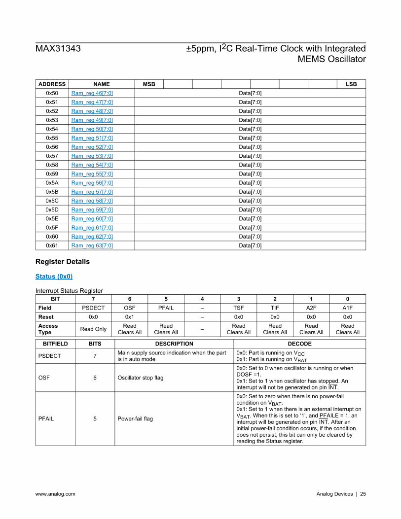
ADDRESS NAME MSB LSB 0x50 Ram_reg 46[7:0] Data[7:0] 0x51 Ram_reg 47[7:0] Data[7:0] 0x52 Ram_reg 48[7:0] Data[7:0] 0x53 Ram_reg 49[7:0] Data[7:0] 0x54 Ram_reg 50[7:0] Data[7:0] 0x55 Ram_reg 51[7:0] Data[7:0] 0x56 Ram_reg 52[7:0] Data[7:0] 0x57 Ram_reg 53[7:0] Data[7:0] 0x58 Ram_reg 54[7:0] Data[7:0] 0x59 Ram_reg 55[7:0] Data[7:0] 0x5A Ram_reg 56[7:0] Data[7:0] 0x5B Ram_reg 57[7:0] Data[7:0] 0x5C Ram_reg 58[7:0] Data[7:0] 0x5D Ram_reg 59[7:0] Data[7:0] 0x5E Ram_reg 60[7:0] Data[7:0] 0x5F Ram_reg 61[7:0] Data[7:0] 0x60 Ram_reg 62[7:0] Data[7:0] 0x61 Ram_reg 63[7:0] Data[7:0]
Register Details
Status (0x0)
Interrupt Status Register BIT 7 6 5 4 3 2 1 0
Field PSDECT OSF PFAIL – TSF TIF A2F A1F Reset 0x0 0x1 – 0x0 0x0 0x0 0x0 Access Type Read Only Read
Clears All Read
Clears All – Read Clears All
Read Clears All
Read Clears All
Read Clears All
BITFIELD BITS DESCRIPTION DECODE
PSDECT 7 Main supply source indication when the part is in auto mode
0x0: Part is running on VCC 0x1: Part is running on VBAT
OSF 6 Oscillator stop flag
0x0: Set to 0 when oscillator is running or when DOSF =1. 0x1: Set to 1 when oscillator has stopped. An interrupt will not be generated on pin INT.
PFAIL 5 Power-fail flag
0x0: Set to zero when there is no power-fail condition on VBAT. 0x1: Set to 1 when there is an external interrupt on VBAT. When this is set to ‘1’, and PFAILE = 1, an interrupt will be generated on pin INT. After an initial power-fail condition occurs, if the condition does not persist, this bit can only be cleared by reading the Status register.
MAX31343 ±5ppm, I2C Real-Time Clock with IntegratedMEMS Oscillator
www.analog.com Analog Devices | 25

BITFIELD BITS DESCRIPTION DECODE
TSF 3 Temp sense data flag: Indicates when user requested temp measurement is ready.(Only applicable in oneshot mode )
0x0: TS data not ready 0x1: Set to 1 when TS data ready. When this is set to ‘1’, and TSIE = 1, an interrupt will be generated on pin INT.
TIF 2 Timer interrupt flag
0x0: Set to zero when count down timer is not zero. 0x1: Set to 1 when countdown timer reaches to zero. When this is set to ‘1’, and TIE = 1, an interrupt will be generated on pin INT.
A2F 1 Alarm2 interrupt flag
0x0: Set to zero when RTC time doesn't match to alarm2 register. 0x1: Set to 1 when RTC time matches the alarm2 register.
When this bit is set, and A2IE = 1, an interrupt will be generated on INT.
A1F 0 Alarm1 Interrupt flag 0x0: When set to zero resets the digital block. 0x1: When set one then device is not on reset mode.
Int_en (0x1)
Interrupt Enable Register BIT 7 6 5 4 3 2 1 0
Field – DOSF PFAILE – TSIE TIE A2IE A1IE Reset – 0x0 0x0 – 0x0 0x0 0x0 0x0 Access Type – Write, Read Write, Read – Write, Read Write, Read Write, Read Write, Read
BITFIELD BITS DESCRIPTION DECODE
DOSF 6 Disable oscillator flag 0x0: Allow the OSF to indicate the oscillator status. 0x1: Disable the oscillator flag, irrespective of the oscillator status.
PFAILE 5 Power fail Interrupt enable
0x0: When set to zero, analog interrupt function is disabled. 0x1: When set to one, analog interrupt function is enabled.
TSIE 3 Temp sense ready flag enable 0x0: Disable temp sense ready function 0x1: Enable temp sense ready function
TIE 2 Timer interrupt enable 0x0: Disable timer interrupt function 0x1: Enable timer interrupt function
A2IE 1 Alarm2 interrupt enable 0x0: Disable alarm2 interrupt function 0x1: Enable alarm2 interrupt function
A1IE 0 Alarm1 interrupt enable 0x0: Disable alarm1 interrupt function 0x1: Enable alarm1 interrupt function
RTC_reset (0x2)
RTC Software Reset Register
MAX31343 ±5ppm, I2C Real-Time Clock with IntegratedMEMS Oscillator
www.analog.com Analog Devices | 26
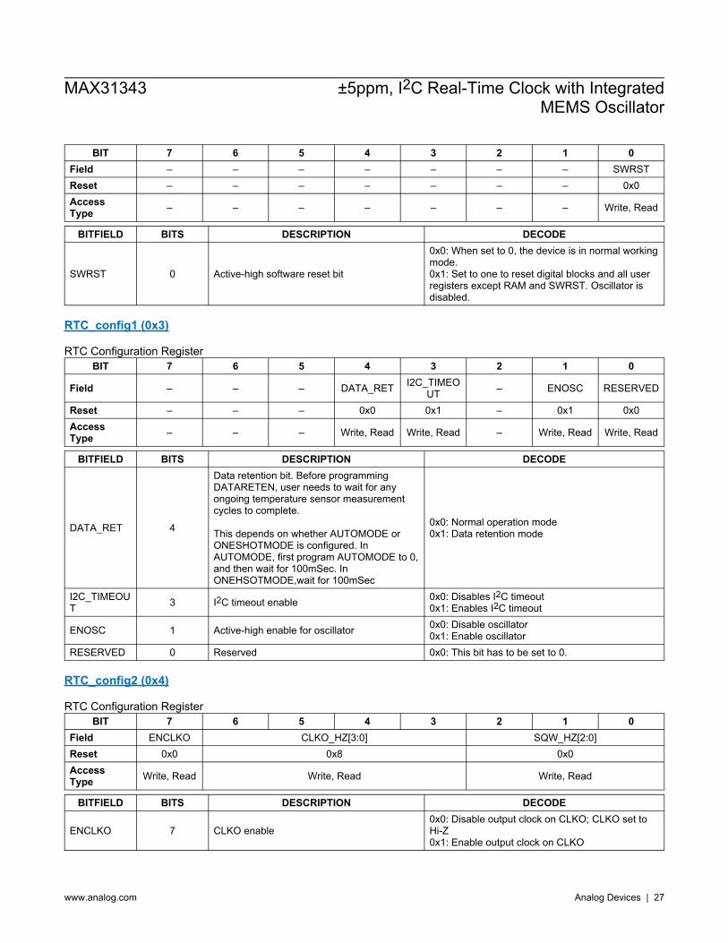
BIT 7 6 5 4 3 2 1 0 Field – – – – – – – SWRST Reset – – – – – – – 0x0 Access Type – – – – – – – Write, Read
BITFIELD BITS DESCRIPTION DECODE
SWRST 0 Active-high software reset bit
0x0: When set to 0, the device is in normal working mode. 0x1: Set to one to reset digital blocks and all user registers except RAM and SWRST. Oscillator is disabled.
RTC_config1 (0x3)
RTC Configuration Register BIT 7 6 5 4 3 2 1 0
Field – – – DATA_RET I2C_TIMEOUT – ENOSC RESERVED
Reset – – – 0x0 0x1 – 0x1 0x0 Access Type – – – Write, Read Write, Read – Write, Read Write, Read
BITFIELD BITS DESCRIPTION DECODE
DATA_RET 4
Data retention bit. Before programming DATARETEN, user needs to wait for any ongoing temperature sensor measurement cycles to complete.
This depends on whether AUTOMODE or ONESHOTMODE is configured. In AUTOMODE, first program AUTOMODE to 0, and then wait for 100mSec. In ONEHSOTMODE,wait for 100mSec
0x0: Normal operation mode 0x1: Data retention mode
I2C_TIMEOUT 3 I2C timeout enable 0x0: Disables I2C timeout
0x1: Enables I2C timeout
ENOSC 1 Active-high enable for oscillator 0x0: Disable oscillator 0x1: Enable oscillator
RESERVED 0 Reserved 0x0: This bit has to be set to 0.
RTC_config2 (0x4)
RTC Configuration Register BIT 7 6 5 4 3 2 1 0
Field ENCLKO CLKO_HZ[3:0] SQW_HZ[2:0] Reset 0x0 0x8 0x0 Access Type Write, Read Write, Read Write, Read
BITFIELD BITS DESCRIPTION DECODE
ENCLKO 7 CLKO enable 0x0: Disable output clock on CLKO; CLKO set to Hi-Z 0x1: Enable output clock on CLKO
MAX31343 ±5ppm, I2C Real-Time Clock with IntegratedMEMS Oscillator
www.analog.com Analog Devices | 27
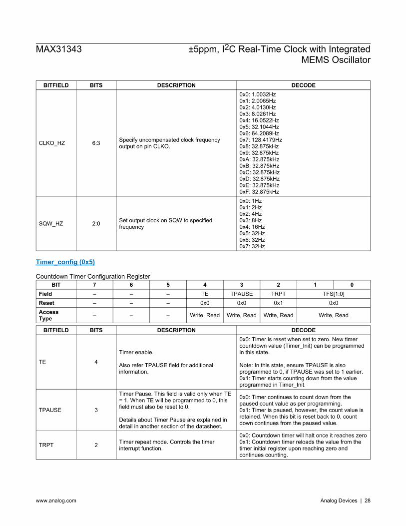
BITFIELD BITS DESCRIPTION DECODE
CLKO_HZ 6:3 Specify uncompensated clock frequency output on pin CLKO.
0x0: 1.0032Hz 0x1: 2.0065Hz 0x2: 4.0130Hz 0x3: 8.0261Hz 0x4: 16.0522Hz 0x5: 32.1044Hz 0x6: 64.2089Hz 0x7: 128.4179Hz 0x8: 32.875kHz 0x9: 32.875kHz 0xA: 32.875kHz 0xB: 32.875kHz 0xC: 32.875kHz 0xD: 32.875kHz 0xE: 32.875kHz 0xF: 32.875kHz
SQW_HZ 2:0 Set output clock on SQW to specified frequency
0x0: 1Hz 0x1: 2Hz 0x2: 4Hz 0x3: 8Hz 0x4: 16Hz 0x5: 32Hz 0x6: 32Hz 0x7: 32Hz
Timer_config (0x5)
Countdown Timer Configuration Register BIT 7 6 5 4 3 2 1 0
Field – – – TE TPAUSE TRPT TFS[1:0] Reset – – – 0x0 0x0 0x1 0x0 Access Type – – – Write, Read Write, Read Write, Read Write, Read
BITFIELD BITS DESCRIPTION DECODE
TE 4
Timer enable.
Also refer TPAUSE field for additional information.
0x0: Timer is reset when set to zero. New timer countdown value (Timer_Init) can be programmed in this state.
Note: In this state, ensure TPAUSE is also programmed to 0, if TPAUSE was set to 1 earlier. 0x1: Timer starts counting down from the value programmed in Timer_Init.
TPAUSE 3
Timer Pause. This field is valid only when TE = 1. When TE will be programmed to 0, this field must also be reset to 0.
Details about Timer Pause are explained in detail in another section of the datasheet.
0x0: Timer continues to count down from the paused count value as per programming. 0x1: Timer is paused, however, the count value is retained. When this bit is reset back to 0, count down continues from the paused value.
TRPT 2 Timer repeat mode. Controls the timer interrupt function.
0x0: Countdown timer will halt once it reaches zero 0x1: Countdown timer reloads the value from the timer initial register upon reaching zero and continues counting.
MAX31343 ±5ppm, I2C Real-Time Clock with IntegratedMEMS Oscillator
www.analog.com Analog Devices | 28

BITFIELD BITS DESCRIPTION DECODE
TFS 1:0 Timer frequency selection
0x0: 1024Hz 0x1: 256Hz 0x2: 64Hz 0x3: 16Hz
Seconds (0x6)
Seconds Configuration Register BIT 7 6 5 4 3 2 1 0
Field – sec_10[2:0] seconds[3:0] Reset – 0x0 0x0 Access Type – Write, Read Write, Read
BITFIELD BITS DESCRIPTION sec_10 6:4 RTC seconds in multiples of 10 seconds 3:0 RTC seconds value.
Minutes (0x7)
Minutes Configuration Register BIT 7 6 5 4 3 2 1 0
Field – min_10[2:0] minutes[3:0] Reset – 0x0 0x0 Access Type – Write, Read Write, Read
BITFIELD BITS DESCRIPTION min_10 6:4 RTC minutes in multiples of 10 minutes 3:0 RTC minutes value
Hours (0x8)
Hours Configuration Register BIT 7 6 5 4 3 2 1 0
Field – – hr_10[1:0] hour[3:0] Reset – – 0x0 0x0 Access Type – – Write, Read Write, Read
BITFIELD BITS DESCRIPTION hr_10 5:4 RTC hours in multiples of 10 hour 3:0 RTC hours value
Day (0x9)
Day Configuration Register
MAX31343 ±5ppm, I2C Real-Time Clock with IntegratedMEMS Oscillator
www.analog.com Analog Devices | 29
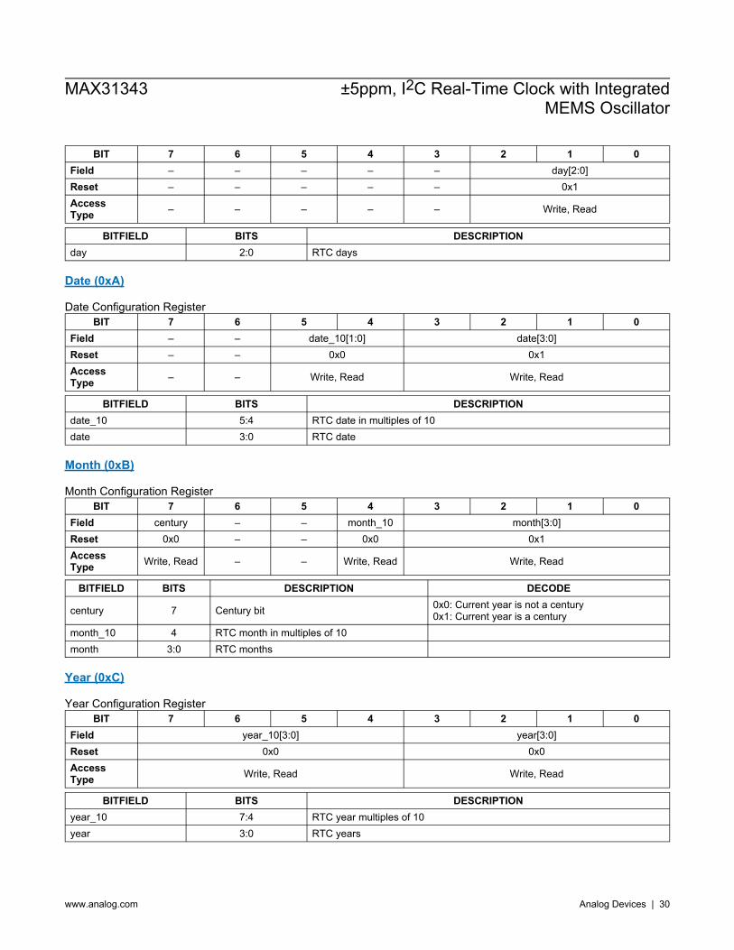
BIT 7 6 5 4 3 2 1 0 Field – – – – – day[2:0] Reset – – – – – 0x1 Access Type – – – – – Write, Read
BITFIELD BITS DESCRIPTION day 2:0 RTC days
Date (0xA)
Date Configuration Register BIT 7 6 5 4 3 2 1 0
Field – – date_10[1:0] date[3:0] Reset – – 0x0 0x1 Access Type – – Write, Read Write, Read
BITFIELD BITS DESCRIPTION date_10 5:4 RTC date in multiples of 10 date 3:0 RTC date
Month (0xB)
Month Configuration Register BIT 7 6 5 4 3 2 1 0
Field century – – month_10 month[3:0] Reset 0x0 – – 0x0 0x1 Access Type Write, Read – – Write, Read Write, Read
BITFIELD BITS DESCRIPTION DECODE
century 7 Century bit 0x0: Current year is not a century 0x1: Current year is a century
month_10 4 RTC month in multiples of 10 month 3:0 RTC months
Year (0xC)
Year Configuration Register BIT 7 6 5 4 3 2 1 0
Field year_10[3:0] year[3:0] Reset 0x0 0x0 Access Type Write, Read Write, Read
BITFIELD BITS DESCRIPTION year_10 7:4 RTC year multiples of 10 year 3:0 RTC years
MAX31343 ±5ppm, I2C Real-Time Clock with IntegratedMEMS Oscillator
www.analog.com Analog Devices | 30

Alm1_sec (0xD)
DY_DT A1M6 A1M5 A1M4 A1M3 A1M2 A1M1 ALARM RATE x 1 1 1 1 1 1 Once per sec x 1 1 1 1 1 0 Sec match x 1 1 1 1 0 0 Min and sec match x 1 1 1 0 0 0 Hour, min, and sec match 0 1 1 0 0 0 0 Date and Time match 0 1 0 0 0 0 0 Month, Date, and Time match 0 0 0 0 0 0 0 Year, Month, Date, and Time match 1 1 1 0 0 0 0 Day and Time match
Alarm 1 can be set by writing to registers 0Dh - 12h. See register map. The alarm can be programmed by the A1IE bit in Int_en reg (01h) register to activate the INT output on an alarm match condition. Bit 7 of each of the time-of-day/ date alarm registers, and Bit 7 & 6 of month alarm register are mask bits. When all the mask bits of each alarm are logic 0, an alarm only occurs when the values in the timekeeping registers match the corresponding values stored in the time-of-day/date alarm registers. The alarm can also be programmed to repeat every second, minute, hour, day, date, month, or year. Table above, shows the possible settings. Configurations not listed in the table result in illogical operation. The DY_DT bit (bit 6 of the alarm day/date registers) control whether the alarm value stored in bits 0-5 that register reflects the day of the week or the date of the month. If DY_DT is written to logic 0, the alarm is the result of a match with date of the month. If DY_DT is written to logic 1, the alarm is the result of a match with day of the week.
BIT 7 6 5 4 3 2 1 0 Field A1M1 sec_10[2:0] seconds[3:0] Reset 0x0 0x0 0x0 Access Type Write, Read Write, Read Write, Read
BITFIELD BITS DESCRIPTION A1M1 7 Alarm1 mask bit for seconds sec_10 6:4 Alarm1 seconds in multiples of 10 seconds 3:0 Alarm1 seconds
Alm1_min (0xE)
Alarm1 Minutes Configuration Register BIT 7 6 5 4 3 2 1 0
Field A1M2 min_10[2:0] minutes[3:0] Reset 0x0 0x0 0x0 Access Type Write, Read Write, Read Write, Read
BITFIELD BITS DESCRIPTION A1M2 7 Alarm1 mask bit for minutes min_10 6:4 Alarm1 minutes in multiples of 10 minutes 3:0 Alarm1 minutes
Alm1_hrs (0xF)
Alarm1 Hours Configuration Register
MAX31343 ±5ppm, I2C Real-Time Clock with IntegratedMEMS Oscillator
www.analog.com Analog Devices | 31
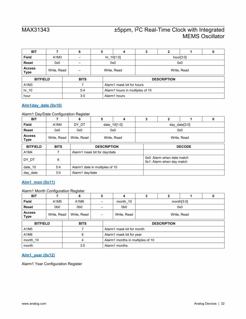
BIT 7 6 5 4 3 2 1 0 Field A1M3 – hr_10[1:0] hour[3:0] Reset 0x0 – 0x0 0x0 Access Type Write, Read – Write, Read Write, Read
BITFIELD BITS DESCRIPTION A1M3 7 Alarm1 mask bit for hours hr_10 5:4 Alarm1 hours in multiples of 10 hour 3:0 Alarm1 hours
Alm1day_date (0x10)
Alarm1 Day/Date Configuration Register BIT 7 6 5 4 3 2 1 0
Field A1M4 DY_DT date_10[1:0] day_date[3:0] Reset 0x0 0x0 0x0 0x0 Access Type Write, Read Write, Read Write, Read Write, Read
BITFIELD BITS DESCRIPTION DECODE A1M4 7 Alarm1 mask bit for day/date
DY_DT 6 0x0: Alarm when date match 0x1: Alarm when day match
date_10 5:4 Alarm1 date in multiples of 10 day_date 3:0 Alarm1 day/date
Alm1_mon (0x11)
Alarm1 Month Configuration Register BIT 7 6 5 4 3 2 1 0
Field A1M5 A1M6 – month_10 month[3:0] Reset 0b0 0b0 – 0b0 0x0 Access Type Write, Read Write, Read – Write, Read Write, Read
BITFIELD BITS DESCRIPTION A1M5 7 Alarm1 mask bit for month A1M6 6 Alarm1 mask bit for year month_10 4 Alarm1 months in multiples of 10 month 3:0 Alarm1 months
Alm1_year (0x12)
Alarm1 Year Configuration Register
MAX31343 ±5ppm, I2C Real-Time Clock with IntegratedMEMS Oscillator
www.analog.com Analog Devices | 32

BIT 7 6 5 4 3 2 1 0 Field year_10[3:0] year[3:0] Reset 0x0 0x0 Access Type Write, Read Write, Read
BITFIELD BITS DESCRIPTION year_10 7:4 Alarm1 year in multiples of 10 year 3:0 Alarm1 years
Alm2_min (0x13)
Alarm 2 can be set by writing to registers 13h - 15h. See register map. The alarm can be programmed by the A2IE bit in Int_en reg (01h) register to activate the INT output on an alarm match condition. Bit 7 of each of the time-of-day/ date alarm registers are mask bits. When all the mask bits of each alarm are logic 0, an alarm only occurs when the values in the timekeeping registers match the corresponding values stored in the time-of-day/date alarm registers. The alarm can also be programmed to repeat every minute, hour, day, or date. Table below, shows the possible settings. Configurations not listed in the table result in illogical operation. The DY_DT bit (bit 6 of the alarm day/date registers) control whether the alarm value stored in bits 0-5 that register reflects the day of the week or the date of the month. If DY_DT is written to logic 0, the alarm is the result of a match with date of the month. If DY_DT is written to logic 1, the alarm is the result of a match with day of the week. DY_DT A2M4 A2M3 A2M2 ALARM RATE x 1 1 1 Once per minute x 1 1 0 Minute match x 1 0 0 Hour and minute match 0 0 0 0 Date, hour, and minute match 1 0 0 0 Day, hour, and minute match
BIT 7 6 5 4 3 2 1 0 Field A2M2 min_10[2:0] minutes[3:0] Reset 0x0 0x0 0x0 Access Type Write, Read Write, Read Write, Read
BITFIELD BITS DESCRIPTION A2M2 7 Alarm2 mask bit for minutes min_10 6:4 Alarm2 minutes in multiples of 10 minutes 3:0 Alarm2 minutes
Alm2_hrs (0x14)
Alarm2 Hours Configuration Register BIT 7 6 5 4 3 2 1 0
Field A2M3 – hr_10[1:0] hour[3:0] Reset 0x0 – 0x0 0x0 Access Type Write, Read – Write, Read Write, Read
BITFIELD BITS DESCRIPTION A2M3 7 Alarm2 mask bit for hours
MAX31343 ±5ppm, I2C Real-Time Clock with IntegratedMEMS Oscillator
www.analog.com Analog Devices | 33
BITFIELD BITS DESCRIPTION hr_10 5:4 Alarm2 hours in multiples of 10 hour 3:0 Alarm2 hours
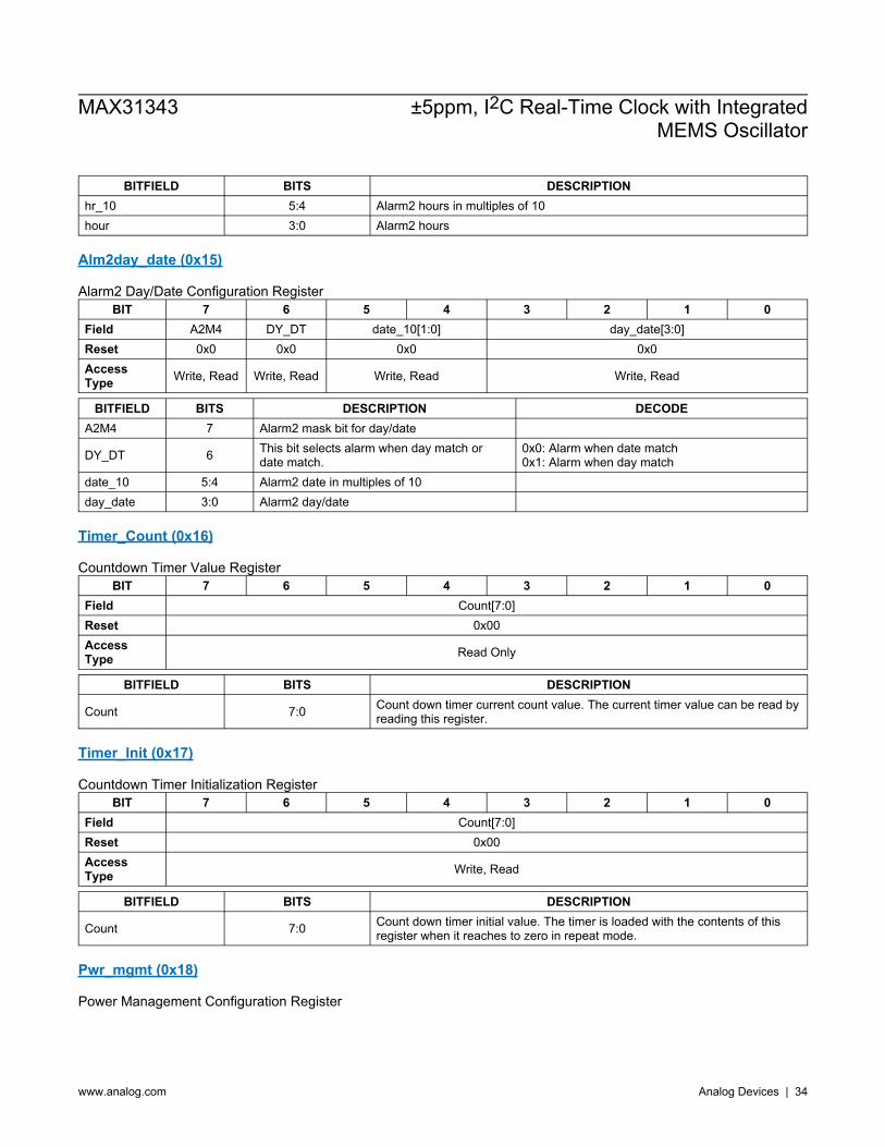
Alm2day_date (0x15)
Alarm2 Day/Date Configuration Register BIT 7 6 5 4 3 2 1 0
Field A2M4 DY_DT date_10[1:0] day_date[3:0] Reset 0x0 0x0 0x0 0x0 Access Type Write, Read Write, Read Write, Read Write, Read
BITFIELD BITS DESCRIPTION DECODE A2M4 7 Alarm2 mask bit for day/date
DY_DT 6 This bit selects alarm when day match or date match.
0x0: Alarm when date match 0x1: Alarm when day match
date_10 5:4 Alarm2 date in multiples of 10 day_date 3:0 Alarm2 day/date
Timer_Count (0x16)
Countdown Timer Value Register BIT 7 6 5 4 3 2 1 0
Field Count[7:0] Reset 0x00 Access Type Read Only
BITFIELD BITS DESCRIPTION
Count 7:0 Count down timer current count value. The current timer value can be read by reading this register.
Timer_Init (0x17)
Countdown Timer Initialization Register BIT 7 6 5 4 3 2 1 0
Field Count[7:0] Reset 0x00 Access Type Write, Read
BITFIELD BITS DESCRIPTION
Count 7:0 Count down timer initial value. The timer is loaded with the contents of this register when it reaches to zero in repeat mode.
Pwr_mgmt (0x18)
Power Management Configuration Register
MAX31343 ±5ppm, I2C Real-Time Clock with IntegratedMEMS Oscillator
www.analog.com Analog Devices | 34
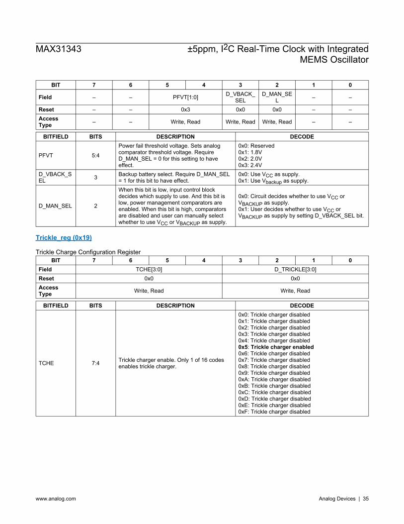
BIT 7 6 5 4 3 2 1 0
Field – – PFVT[1:0] D_VBACK_SEL
D_MAN_SEL – –
Reset – – 0x3 0x0 0x0 – – Access Type – – Write, Read Write, Read Write, Read – –
BITFIELD BITS DESCRIPTION DECODE
PFVT 5:4
Power fail threshold voltage. Sets analog comparator threshold voltage. Require D_MAN_SEL = 0 for this setting to have effect.
0x0: Reserved 0x1: 1.8V 0x2: 2.0V 0x3: 2.4V
D_VBACK_SEL 3 Backup battery select. Require D_MAN_SEL
= 1 for this bit to have effect. 0x0: Use VCC as supply. 0x1: Use Vbackup as supply.
D_MAN_SEL 2
When this bit is low, input control block decides which supply to use. And this bit is low, power management comparators are enabled. When this bit is high, comparators are disabled and user can manually select whether to use VCC or VBACKUP as supply.
0x0: Circuit decides whether to use VCC or VBACKUP as supply. 0x1: User decides whether to use VCC or VBACKUP as supply by setting D_VBACK_SEL bit.
Trickle_reg (0x19)
Trickle Charge Configuration Register BIT 7 6 5 4 3 2 1 0
Field TCHE[3:0] D_TRICKLE[3:0] Reset 0x0 0x0 Access Type Write, Read Write, Read
BITFIELD BITS DESCRIPTION DECODE
TCHE 7:4 Trickle charger enable. Only 1 of 16 codes enables trickle charger.
0x0: Trickle charger disabled 0x1: Trickle charger disabled 0x2: Trickle charger disabled 0x3: Trickle charger disabled 0x4: Trickle charger disabled 0x5: Trickle charger enabled 0x6: Trickle charger disabled 0x7: Trickle charger disabled 0x8: Trickle charger disabled 0x9: Trickle charger disabled 0xA: Trickle charger disabled 0xB: Trickle charger disabled 0xC: Trickle charger disabled 0xD: Trickle charger disabled 0xE: Trickle charger disabled 0xF: Trickle charger disabled
MAX31343 ±5ppm, I2C Real-Time Clock with IntegratedMEMS Oscillator
www.analog.com Analog Devices | 35
BITFIELD BITS DESCRIPTION DECODE
D_TRICKLE 3:0 Sets the charging path for trickle charger. Must set TCHE to 0x5 to enable the setting below.
0x0: 3KΩ in series with a Schottky diode 0x1: 3KΩ in series with a Schottky diode 0x2: 6KΩ in series with a Schottky diode 0x3: 11KΩ in series with a Schottky diode 0x4: 3KΩ in series with a diode+Schottky diode 0x5: 3KΩ in series with a diode+Schottky diode 0x6: 6KΩ in series with a diode+Schottky diode 0x7: 11KΩ in series with a diode+Schottky diode 0x8: No Connection 0x9: No Connection 0xA: No Connection 0xB: No Connection 0xC: No Connection 0xD: No Connection 0xE: No Connection 0xF: No Connection
Temp_MSB (0x1A)
Temperature sensor measurement is stored as a 10-bit two’s complement number in two-byte temperature register. SIGN bit indicates if the temperature is positive or negative. When SIGN bit is 1, it represents negative temperature, and it has a weight of -128. Bit [5:0] are redundant. Bit 6 of Temperature [15:0] is LSB and has a weight of 0.25. Table below represent weight of each bit from Bit 6 to Bit 14. Temperature Register Definition MSB LSB D15 D14 D13 D12 D11 D10 D9 D8 D7 D6 D5 D4 D3 D2 D1 D0 SIGN 64ºC 32ºC 16ºC 8ºC 4ºC 2ºC 1ºC 0.5ºC 0.25ºC 0 0 0 0 0 0
Temperature Format Examples TEMPERATURE (°C) Temp MSB [15:8] Temp LSB [7:0] 85ºC 0101 0101 0000 0000 84.75ºC 0101 0100 1100 0000 0ºC 0000 0000 0000 0000 -0.25ºC 1111 1111 1100 0000 -40ºC 1101 1000 0000 0000
Assuming user reads Temp_MSB and Temp_LSB registers as Temp_MSB = 8'b01010100, Temp_LSB = 8'b11000000. Per Table above, Bit 15 = 0 means positive temperature, 64X1 + 32X0 + 16X1 + 8X0 + 4X1 + 2X0 + 1X0 = 84ºC, 0.5X1 + 0.25X1 = 0.75ºC. Hence, temperature = 84.75ºC.
BIT 7 6 5 4 3 2 1 0 Field Temperature[15:8] Reset Access Type Read Only
BITFIELD BITS DESCRIPTION
Temperature 7:0 MSB of the 16-bit temperature register
MAX31343 ±5ppm, I2C Real-Time Clock with IntegratedMEMS Oscillator
www.analog.com Analog Devices | 36

Temp_LSB (0x1B)
Temperature Value LSB Register BIT 7 6 5 4 3 2 1 0
Field Temperature[7:0] Reset Access Type Read Only
BITFIELD BITS DESCRIPTION Temperature 7:0 LSB of the 16-bit temperature register.
TS_config (0x1C)
Temperature Sensor Configuration Register BIT 7 6 5 4 3 2 1 0
Field AUTOMODE
ONESHOTMODE TTSINT[2:0] – – –
Reset 0x1 0x0 0x5 – – – Access Type Write, Read Write, Read Write, Read – – –
BITFIELD BITS DESCRIPTION DECODE
AUTOMODE 7
Automatic mode of temperature measurement. This mode is valid only when ONESHOTMODE = 0.
In this mode, temperature measurement interval is decided by TTSINT.
After each temperature measurement request, the divider ratio will be modified for temperature compensation.
0x0: Automatic measurement mode disabled 0x1: Automatic measurement mode enabled
ONESHOTMODE 6
One-shot user-requested temperature measurement in real-time. AUTOMODE must be 0 in one-shot measurement mode.
When this bit is set, divider ratio is updated (compensated) after temperature measurement. This bit is self-cleared after temperature measurement complete; writes to this bit before it has been cleared have no effect.
0x0: No temperature measurement requested 0x1: Temperature measurement requested
TTSINT 5:3 Set temperature measurement interval to specified time for automatic mode of temperature measurement and compensation
0x0: 1sec 0x1: 2sec 0x2: 4sec 0x3: 8sec 0x4: 16sec 0x5: 32sec 0x6: 64sec 0x7: 128sec
Ram_reg (0x22, 0x23, 0x24, 0x25, 0x26, 0x27, 0x28, 0x29, 0x2A, 0x2B, 0x2C, 0x2D, 0x2E, 0x2F, 0x30, 0x31, 0x32, 0x33, 0x34, 0x35, 0x36, 0x37, 0x38, 0x39, 0x3A, 0x3B, 0x3C, 0x3D, 0x3E, 0x3F, 0x40, 0x41, 0x42,
MAX31343 ±5ppm, I2C Real-Time Clock with IntegratedMEMS Oscillator
www.analog.com Analog Devices | 37

0x43, 0x44, 0x45, 0x46, 0x47, 0x48, 0x49, 0x4A, 0x4B, 0x4C, 0x4D, 0x4E, 0x4F, 0x50, 0x51, 0x52, 0x53, 0x54, 0x55, 0x56, 0x57, 0x58, 0x59, 0x5A, 0x5B, 0x5C, 0x5D, 0x5E, 0x5F, 0x60, 0x61)
BIT 7 6 5 4 3 2 1 0 Field Data[7:0] Reset Access Type Write, Read
BITFIELD BITS DESCRIPTION Data 7:0 RAM data byte
MAX31343 ±5ppm, I2C Real-Time Clock with IntegratedMEMS Oscillator
www.analog.com Analog Devices | 38
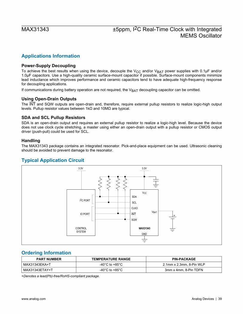
Applications Information
Power-Supply Decoupling To achieve the best results when using the device, decouple the VCC and/or VBAT power supplies with 0.1μF and/or 1.0μF capacitors. Use a high-quality ceramic surface-mount capacitor if possible. Surface-mount components minimize lead inductance which improves performance and ceramic capacitors tend to have adequate high-frequency response for decoupling applications. If communications during battery operation are not required, the VBAT decoupling capacitor can be omitted.
Using Open-Drain Outputs The INT and SQW outputs are open-drain and, therefore, require external pullup resistors to realize logic-high output levels. Pullup resistor values between 1kΩ and 10MΩ are typical.
SDA and SCL Pullup Resistors SDA is an open-drain output and requires an external pullup resistor to realize a logic-high level. Because the device does not use clock cycle stretching, a master using either an open-drain output with a pullup resistor or CMOS output driver (push-pull) could be used for SCL.
Handling The MAX31343 package contains an integrated resonator. Pick-and-place equipment can be used. Ultrasonic cleaning should be avoided to prevent damage to the resonator.
Typical Application Circuit
SDA
SCL
CLKO
INT
SQW
VBAT
I2C PORT
IO PORT
CONTROL SYSTEM
3.3V 3.3V
MAX31343MAX31343
VCC
GND
Ordering Information PART NUMBER TEMPERATURE RANGE PIN-PACKAGE
MAX31343EKA+T -40°C to +85°C 2.1mm x 2.3mm, 8-Pin WLP MAX31343ETAY+T -40°C to +85°C 3mm x 4mm, 8-Pin TDFN
+Denotes a lead(Pb)-free/RoHS-compliant package.
MAX31343 ±5ppm, I2C Real-Time Clock with IntegratedMEMS Oscillator
www.analog.com Analog Devices | 39
Revision History REVISION NUMBER
REVISION DATE DESCRIPTION PAGES
CHANGED 0 12/19 Initial release —
1 4/20 Updated aging performance, frequency accuracy, package dimensions, and storage temperature; updated Data-Retention Mode section; updated Figure 4 1, 6-8, 13, 17, 38
2 9/20 Updated Ordering Information table 38 3 6/21 Updated Package Information and Electrical Characteristics table 6, 8 4 10/21 Updated Electrical Characteristics table and Register Map 6, 9, 26 5 11/21 Updated Table 2 and Register Map 14, 22, 28, 31, 33
Information furnished by Analog Devices is believed to be accurate and reliable. However, no responsibility is assumed by Analog Devices for its use, nor for any infringements of patents or other rights of third parties that may result from its use. Specifications subject to change without notice. No license is granted by implication or otherwise under any patent or patent rights of Analog Devices. Trademarks and registered trademarks are the property of their respective owners.
MAX31343 ±5ppm, I2C Real-Time Clock with IntegratedMEMS Oscillator
w w w . a n a l o g . c o m Analog Devices | 40

Mouser Electronics
Authorized Distributor
Click to View Pricing, Inventory, Delivery & Lifecycle Information: Maxim Integrated:
MAX31343EKA+ MAX31343EKA+T MAX31343ETAY+T MAX31343ETAY+