real-time clock module (i2c bus) - diodes incorporated pt0322-8 06/16/15 3 pt7c4311 real-time clock...
TRANSCRIPT
|||||||||||||||||||||||||||||||||||||||||||||||||||||||||||||||||||||||||||||||||||||||||||||||||||||||||||||||||||||||||||||||||||||||||||||||||||||||||||||||||||||||||||||||||||||||||||||||||||||||||||||||||||||||||||||||||||||||||||||||||||||||||||||||||||||||||||||||||||||||||||||||||||||||||||||||||||||||||||||||||||||||
Real-time Clock Module (I2C Bus)
2015-06-0002 PT0322-8 06/16/15
1
PT7C4311
Features
Support I2C-Bus (High speed mode 400kHz)
Includes time (Hour/Minute/Second) and calendar
(Century/Year/Month/Date/Day) counter functions
Year 2000 compliant
Automatic switch-over and deselect circuitry
Time keeping voltage: 1.2V to 5.5V
Software clock calibration
56 bytes of general purpose RAM
Ultra-low battery supply current of 0.3A
Low operating current of 70A
Battery or super cap back-up
Operating temperature: -40°C to 85°C
Automatic leap year compensation
Special software programmable output
Description
The PT7C4311 serial real-time clock is a low-power
clock/calendar with a programmable square-wave output.
Address and data are transferred serially via a 2-wire
bidirectional bus. The clock/calendar provides seconds,
minutes, hours, day, date, month, and year information.
The date at the end of the month is automatically
adjusted for months with fewer than 31 days, including
corrections for leap year. The clock operates in the 24-
hour format indicator.
Table 1 shows the basic functions of PT7C4311. More
details are shown in section: overview of functions.
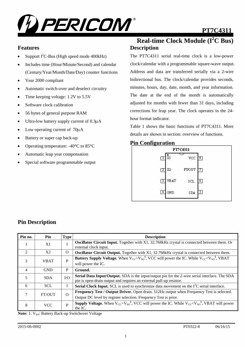
Pin Configuration
Pin Description
Pin no. Pin Type Description
1 X1 I Oscillator Circuit Input. Together with X1, 32.768kHz crystal is connected between them. Or
external clock input.
2 X2 O Oscillator Circuit Output. Together with X1, 32.768kHz crystal is connected between them.
3 VBAT P Battery Supply Voltage. When VCC>VSO
1, VCC will power the IC. While VCC<VSO
1, VBAT
will power the IC.
4 GND P Ground.
5 SDA I/O Serial Data Input/Output. SDA is the input/output pin for the 2-wire serial interface. The SDA
pin is open-drain output and requires an external pull-up resistor.
6 SCL I Serial Clock Input. SCL is used to synchronize data movement on the I2C serial interface.
7 FT/OUT O Frequency Test / Output Driver. Open drain. 512Hz output when Frequency Test is selected.
Output DC level by register selection. Frequency Test is prior.
8 VCC P Supply Voltage. When VCC>VSO
1, VCC will power the IC. While VCC<VSO
1, VBAT will power
the IC.
Note: 1. VSO: Battery Back-up Switchover Voltage
|||||||||||||||||||||||||||||||||||||||||||||||||||||||||||||||||||||||||||||||||||||||||||||||||||||||||||||||||||||||||||||||||||||||||||||||||||||||||||||||||||||||||||||||||||||||||||||||||||||||||||||||||||||||||||||||||||||||||||||||||||||||||||||||||||||||||||||||||||||||||||||||||||||||||||||||||||||||||||||||||||||||
2015-06-0002 PT0322-8 06/16/15
2
PT7C4311
Real-time Clock Module (I2C Bus)
Table 1. Basic functions of PT7C4311
Item Function PT7C4311
1 Oscillator
Source: Crystal: 32.768kHz
Oscillator enable/disable
Oscillator fail detect -
2 Time
Time display 12-hour -
24-hour
Century bit
Time count chain enable/disable -
3 Programmable square wave output (Hz) 512Hz
4 Programmable high/low level output
5 Communication 2-wire I2C bus
6 RAM 568
7 Battery backup
8 Clock calibration
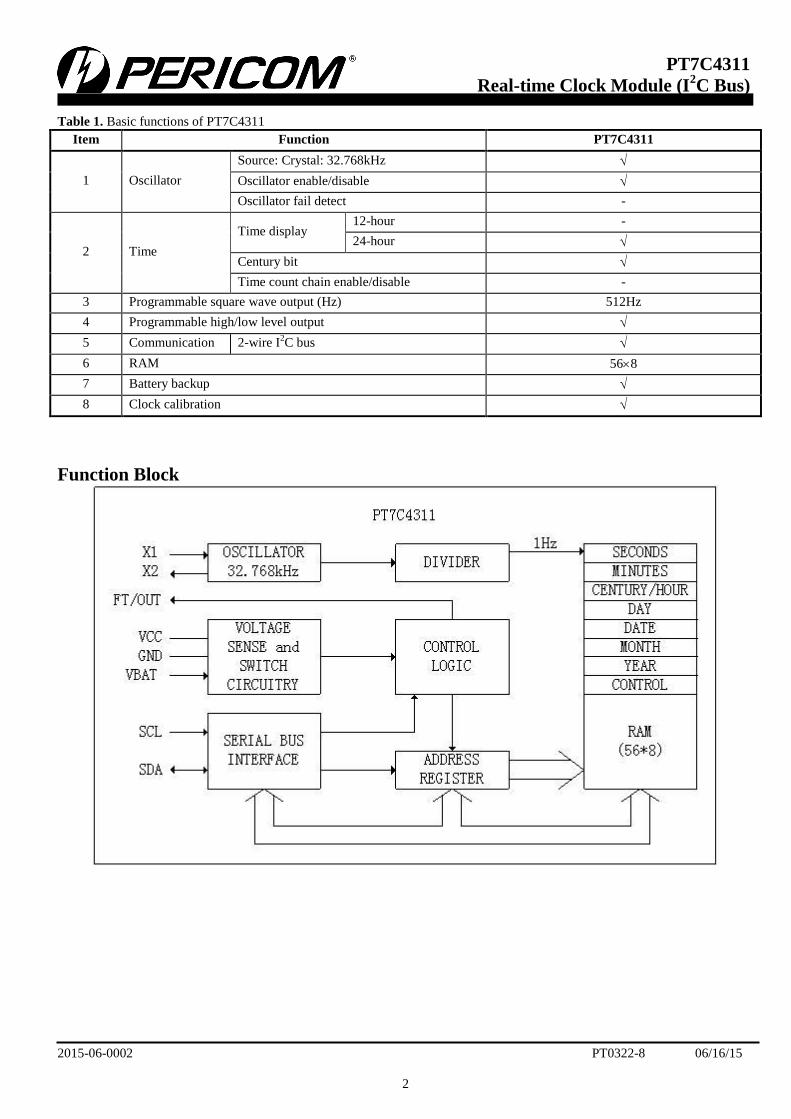
Function Block
|||||||||||||||||||||||||||||||||||||||||||||||||||||||||||||||||||||||||||||||||||||||||||||||||||||||||||||||||||||||||||||||||||||||||||||||||||||||||||||||||||||||||||||||||||||||||||||||||||||||||||||||||||||||||||||||||||||||||||||||||||||||||||||||||||||||||||||||||||||||||||||||||||||||||||||||||||||||||||||||||||||||
2015-06-0002 PT0322-8 06/16/15
3
PT7C4311
Real-time Clock Module (I2C Bus)
Maximum Ratings
Storage Temperature ............................................................................................................... -55oCto +125oC
Ambient Temperature with Power Applied ...................................................................... -40oCto +85oC
Supply Voltage to Ground Potential (Vcc to GND) ...................................................... -0.3V to +7.0V
DC Input (All Other Inputs except Vcc & GND) ........................................................... -0.3V to +7.0V
DC Output Voltage ................................................................................................................. -0.3V to +7.0V
Power Dissipation .................................................................................................................... 250mW
Output Current .......................................................................................................................... 20mA
Note:
Stresses greater than those listed under MAXIMUM RATINGS may cause permanent damage to the device. This is a stress rating
only and functional operation of the device at these or any other conditions above those indicated in the operational sections of
this specification is not implied. Exposure to absolute maximum rating conditions for extended periods may affect reliability.
Recommended Operating Conditions
Symbol Description Min Type Max Unit
VCC
Timing data and RAM data maintaining voltage 1.2 - 5.5
V
Timing data writing voltage 1.5 - 5.5
Timing data reading voltage 1.5 - 5.5
RAM data writing voltage 3.0 - 5.5
RAM data reading voltage 1.5 - 5.5
VIH Input high level 0.7 VCC - VCC+0.3
VIL Input low level -0.3 - 0.3 VCC
TA Operating temperature -40 - 85 ºC
|||||||||||||||||||||||||||||||||||||||||||||||||||||||||||||||||||||||||||||||||||||||||||||||||||||||||||||||||||||||||||||||||||||||||||||||||||||||||||||||||||||||||||||||||||||||||||||||||||||||||||||||||||||||||||||||||||||||||||||||||||||||||||||||||||||||||||||||||||||||||||||||||||||||||||||||||||||||||||||||||||||||
2015-06-0002 PT0322-8 06/16/15
4
PT7C4311
Real-time Clock Module (I2C Bus)
DC Electrical Characteristics
(Unless otherwise specified, VCC = 1.5 ~ 5.5 V, TA = -40 °C to +85 °C.)
Sym. Description Pin Condition Min Typ Max Unit
VCC
Timing data and RAM data
maintaining voltage VCC - 1.2 - 5.5
V Timing data writing voltage VCC - 1.5 - 5.5
Timing data reading voltage VCC - 1.5 - 5.5
RAM data writing voltage VCC - 3.0 - 5.5
RAM data reading voltage VCC 1.5 - 5.5
VBAT1
Supply voltage VBAT - 2.0 3 3.56 V
VSO2 Battery Back-up Switchover
Voltage3,4
- -
VBAT -
0.80
VBAT -
0.50
VBAT -
0.305
V
ICC Current consumption VCC Switch freq. = 400kHz - 70 150 A
IST Standby current VCC SDA, SCL = VCC – 0.3V - 25 80 A
IBAT Current consumption VBAT OSC on, VCC = 0V, VBAT = 3V,
TA=25°C - 300 800 nA
VIL Low-level input voltage - - -0.3 - 0.3VCC
V VIH High-level input voltage - - 0.7VCC -
VCC
+0.5
VOL
Low-level output voltage SDA IOL = 3mA - - 0.4
V Pull-up Supply voltage
(Open drain)
FT/
OUT - - - 5.5
IIL Input leakage current SCL 0<VIN<VCC - - 1 A
IOZ Output current when OFF SDA 0<VOUT<VCC - - 1 A
Note:
1. After switchover (VSO), VBAT (min) can be 2.0V for crystal with RS=40k.
2. Switch-over and deselect point.
3. Valid for Ambient Operating Temperature: TA = -40 to 85°C; VCC = 2.0 to 5.5V (except where noted). VCC fall time should
not exceed 5 mV/μs.
4. All voltages referenced to GND.
5. In 3.3V application, if initial battery voltage is ≥ 3.4V, it may be necessary to reduce battery voltage (i.e., through wave
soldering the battery) in order to avoid inadvertent switchover/reselection for VCC – 10% operation.
6. For rechargeable backup, VBAT (max) may be considered to be VCC.
|||||||||||||||||||||||||||||||||||||||||||||||||||||||||||||||||||||||||||||||||||||||||||||||||||||||||||||||||||||||||||||||||||||||||||||||||||||||||||||||||||||||||||||||||||||||||||||||||||||||||||||||||||||||||||||||||||||||||||||||||||||||||||||||||||||||||||||||||||||||||||||||||||||||||||||||||||||||||||||||||||||||
2015-06-0002 PT0322-8 06/16/15
5
PT7C4311
Real-time Clock Module (I2C Bus)
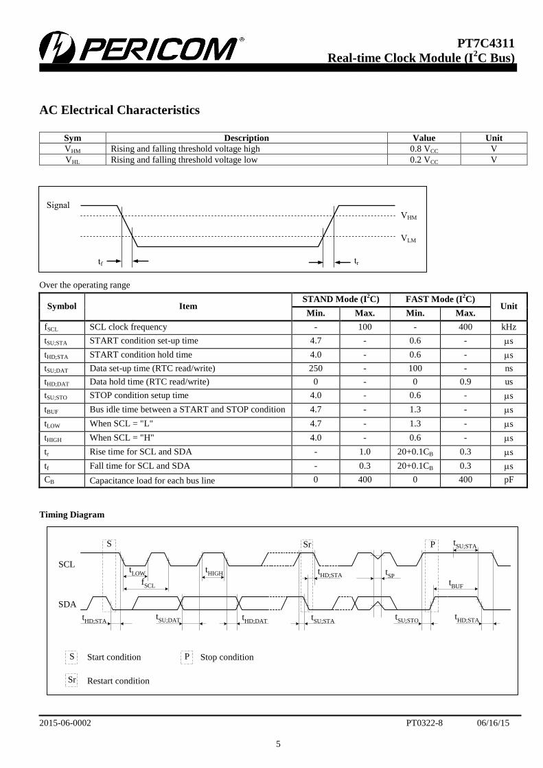
AC Electrical Characteristics
Sym Description Value Unit
VHM Rising and falling threshold voltage high 0.8 VCC V
VHL Rising and falling threshold voltage low 0.2 VCC V
Over the operating range
Symbol Item STAND Mode (I
2C) FAST Mode (I
2C)
Unit Min. Max. Min. Max.
fSCL SCL clock frequency - 100 - 400 kHz
tSU;STA START condition set-up time 4.7 - 0.6 - s
tHD;STA START condition hold time 4.0 - 0.6 - s
tSU;DAT Data set-up time (RTC read/write) 250 - 100 - ns
tHD;DAT Data hold time (RTC read/write) 0 - 0 0.9 us
tSU;STO STOP condition setup time 4.0 - 0.6 - s
tBUF Bus idle time between a START and STOP condition 4.7 - 1.3 - s
tLOW When SCL = "L" 4.7 - 1.3 - s
tHIGH When SCL = "H" 4.0 - 0.6 - s
tr Rise time for SCL and SDA - 1.0 20+0.1CB 0.3 s
tf Fall time for SCL and SDA - 0.3 20+0.1CB 0.3 s
CB Capacitance load for each bus line 0 400 0 400 pF
Timing Diagram
Signal
tf tr
VHM
VLM
S Sr P
tHD;STA t
SP
tSU;DATt
HD;STAtHD;DAT
tSU;STA
tSU;STO
SCL
SDA
tBUF
tHD;STA
tSU;STA
fSCL
tLOW
tHIGH
Sr
S PStart condition
Restart condition
Stop condition
|||||||||||||||||||||||||||||||||||||||||||||||||||||||||||||||||||||||||||||||||||||||||||||||||||||||||||||||||||||||||||||||||||||||||||||||||||||||||||||||||||||||||||||||||||||||||||||||||||||||||||||||||||||||||||||||||||||||||||||||||||||||||||||||||||||||||||||||||||||||||||||||||||||||||||||||||||||||||||||||||||||||
2015-06-0002 PT0322-8 06/16/15
6
PT7C4311
Real-time Clock Module (I2C Bus)
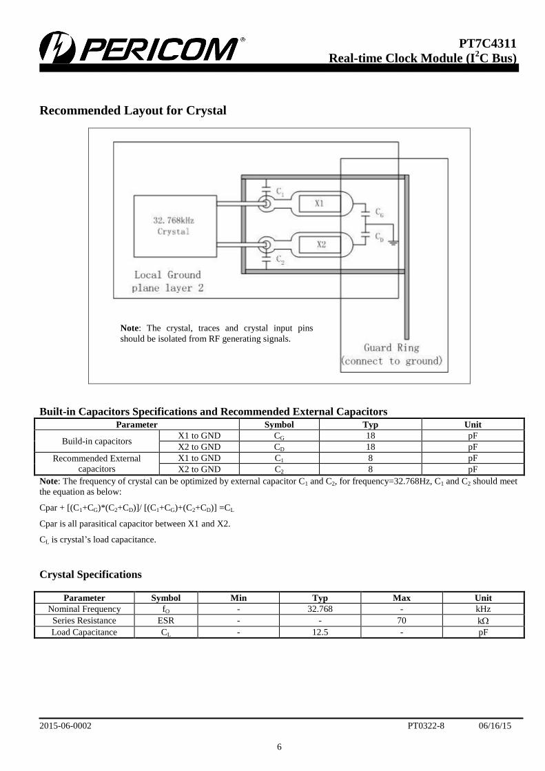
Recommended Layout for Crystal
Built-in Capacitors Specifications and Recommended External Capacitors
Parameter Symbol Typ Unit
Build-in capacitors X1 to GND CG 18 pF
X2 to GND CD 18 pF
Recommended External
capacitors
X1 to GND C1 8 pF
X2 to GND C2 8 pF
Note: The frequency of crystal can be optimized by external capacitor C1 and C2, for frequency=32.768Hz, C1 and C2 should meet
the equation as below:
Cpar + [(C1+CG)*(C2+CD)]/ [(C1+CG)+(C2+CD)] =CL
Cpar is all parasitical capacitor between X1 and X2.
CL is crystal’s load capacitance.
Crystal Specifications
Parameter Symbol Min Typ Max Unit
Nominal Frequency fO - 32.768 - kHz
Series Resistance ESR - - 70 k
Load Capacitance CL - 12.5 - pF
Note: The crystal, traces and crystal input pins
should be isolated from RF generating signals.

|||||||||||||||||||||||||||||||||||||||||||||||||||||||||||||||||||||||||||||||||||||||||||||||||||||||||||||||||||||||||||||||||||||||||||||||||||||||||||||||||||||||||||||||||||||||||||||||||||||||||||||||||||||||||||||||||||||||||||||||||||||||||||||||||||||||||||||||||||||||||||||||||||||||||||||||||||||||||||||||||||||||
2015-06-0002 PT0322-8 06/16/15
7
PT7C4311
Real-time Clock Module (I2C Bus)
Function Description
Overview of Functions
1. Clock function
CPU can read or write data including the year (last two digits), month, date, day, hour, minute, and second. Any (two-digit) year
that is a multiple of 4 is treated as a leap year and calculated automatically as such until the year 2100.
2. Interface with CPU
2-wire I2C interface. The PT7C4311 continually monitors VCC for an out of tolerance condition. Should VCC fall below VSO, the
device terminates an access in progress and resets the device address counter. Inputs to the device will not be recognized at this
time to prevent erroneous data from being written to the device from an out of tolerance system. When VCC falls below VSO, the
device automatically switches from battery to VCC at VSO and recognizes inputs.
3. Oscillator enable/disable
Oscillator and time count chain can be enabled or disabled at the same time by ST bit.
4. Calibration function
With the calibration bits properly set, accuracy PT7C4311 can be improved to better than ±2 ppm at 25°C.
Registers
1. Allocation of registers
Addr.
(hex) *1 Function
Register definition
Bit 7 Bit 6 Bit 5 Bit 4 Bit 3 Bit 2 Bit 1 Bit 0
00 Seconds (00-59) ST*2
S40 S20 S10 S8 S4 S2 S1
01 Minutes (00-59) M40 M20 M10 M8 M4 M2 M1
02 Hours (00-23) CEB*3
CB*3
H20 H10 H8 H4 H2 H1
03 Days of the week (01-07) W4 W2 W1
04 Dates (01-31) D20 D10 D8 D4 D2 D1
05 Months (01-12) *8
MO10 MO8 MO4 MO2 MO1
06 Years (00-99) Y80 Y40 Y20 Y10 Y8 Y4 Y2 Y1
07 Control*8
OUT*4
FT*5
S*6
Calibration*7

|||||||||||||||||||||||||||||||||||||||||||||||||||||||||||||||||||||||||||||||||||||||||||||||||||||||||||||||||||||||||||||||||||||||||||||||||||||||||||||||||||||||||||||||||||||||||||||||||||||||||||||||||||||||||||||||||||||||||||||||||||||||||||||||||||||||||||||||||||||||||||||||||||||||||||||||||||||||||||||||||||||||
2015-06-0002 PT0322-8 06/16/15
8
PT7C4311
Real-time Clock Module (I2C Bus)
08~3F RAM
Caution points:
*1. PT7C4311 uses 6 bits for address. That is if write data to 41H, the data will be written to 01H address register.
*2. Stop bit. When this bit is set to 1, oscillator and time count chain are both stopped.
*3. CEB: Century Enable Bit. CB: Century Bit.
*4. Control FT/OUT pin output DC level when 512Hz square wave is disabled.
*5. Frequency Test. 512Hz square wave output is enabled at FT/OUT pin, which is using for frequency test.
*6. Sign Bit. “1” indicates positive calibration; “0”indicates negative calibration.
*7. Using for modifying count frequency. If 20ppm is wanted to slow down the count frequency, 10 (01010) should be loaded.
*8. Initialize the control and status register to 10000000 if calibration function is not required.
2. Control and status register
Addr.
(hex) Description D7 D6 D5 D4 D3 D2 D1 D0
07 Control OUT FT S Calibration
(default) 1 0 1 Undefined Undefined Undefined Undefined Undefined
a) OUT
OUT: Set pin 7 output DC level..
OUT Data Description
Read / Write 1 Set high level at pin 7.
Default
0 Set low level at pin 7.
b) 512Hz output
FT: 512Hz square wave output Enable bit, using for Frequency Test.
FT Data Description
Read / Write 0 Disable 512Hz output at pin 7.
Default
1 Enable 512Hz output at pin 7.
c) Calibration bits
S: Sign bit.
S Data Description
Read / Write 1 Indicate positive calibration.
Default
0 Indicate negative calibration.
Calibration:
Calibration occurs within a 64minute cycle. The first 62 minutes in the cycle may, once per minute, have one second either
shortened by 128 or lengthened by 256 oscillator cycles. If a binary '1' is loaded into the register, only the first 2
minutes in the 64 minute cycle will be modified; if a binary 6 is loaded, the first 12 will be affected, and so on. Therefore, each
calibration step has the effect of adding 512 or subtracting 256 oscillator cycles for every 125,829,120 actual oscillator cycles, that
is +4.068 or –2.034 ppm of adjustment per calibration step in the calibration register. Assuming that the oscillator is in fact
running at exactly 32,768Hz, each of the 31 increments in the Calibration byte would represent +10.7 or –5.35 seconds per month
which corresponds to a total range of +5.5 or –2.75 minutes per month.
For example, a reading of 512.01024Hz would indicate a +20 ppm oscillator frequency error, requiring a –10 (XX001010) to be
loaded into the Calibration Byte for correction.
|||||||||||||||||||||||||||||||||||||||||||||||||||||||||||||||||||||||||||||||||||||||||||||||||||||||||||||||||||||||||||||||||||||||||||||||||||||||||||||||||||||||||||||||||||||||||||||||||||||||||||||||||||||||||||||||||||||||||||||||||||||||||||||||||||||||||||||||||||||||||||||||||||||||||||||||||||||||||||||||||||||||
2015-06-0002 PT0322-8 06/16/15
9
PT7C4311
Real-time Clock Module (I2C Bus)
Clock calibration
、
3. Time Counter
Time digit display (in BCD code):
Second digits: Range from 00 to 59 and carried to minute digits when incremented from 59 to 00.
Minute digits: Range from 00 to 59 and carried to hour digits when incremented from 59 to 00.
Hour digits: See description on the /12, 24 bit. Carried to day and day-of-the-week digits when incremented from 11 p.m. to
12 a.m. or 23 to 00.
Addr.
(hex) Description D7 D6 D5 D4 D3 D2 D1 D0
00 Seconds ST
S40 S20 S10 S8 S4 S2 S1
(default) 0 Undefined Undefined Undefined Undefined Undefined Undefined Undefined
01 Minutes
*2 M40 M20 M10 M8 M4 M2 M1
(default) 0 Undefined Undefined Undefined Undefined Undefined Undefined Undefined
02 Hours CEB
*3 CB
*3 H20 H10 H8 H4 H2 H1
(default) 1 1 Undefined Undefined Undefined Undefined Undefined Undefined
* Note 1: ST bit: Stop oscillation and time count chain.
* Note 2: Do not care.
* Note 3: Century Enable Bit and Century Bit.
4. Days of the week Counter
The day counter is a divide-by-7 counter that counts from 01 to 07 and up 07 before starting again from 01. Values that
correspond to the day of week are user defined but must be sequential (i.e., if 1 equals Sunday, then 2 equals Monday, and so on).
Illogical time and date entries result in undefined operation.
Addr.
(hex) Description D7 D6 D5 D4 D3 D2 D1 D0
03 Days of the week W4 W2 W1
(default) Undefined Undefined Undefined Undefined Undefined Undefined Undefined Undefined
5. Calendar Counter
The data format is BCD format.
Day digits: Range from 1 to 31 (for January, March, May, July, August, October and December).
Range from 1 to 30 (for April, June, September and November).
Range from 1 to 29 (for February in leap years).
Range from 1 to 28 (for February in ordinary years).
Carried to month digits when cycled to 1.
Month digits: Range from 1 to 12 and carried to year digits when cycled to 1.
|||||||||||||||||||||||||||||||||||||||||||||||||||||||||||||||||||||||||||||||||||||||||||||||||||||||||||||||||||||||||||||||||||||||||||||||||||||||||||||||||||||||||||||||||||||||||||||||||||||||||||||||||||||||||||||||||||||||||||||||||||||||||||||||||||||||||||||||||||||||||||||||||||||||||||||||||||||||||||||||||||||||
2015-06-0002 PT0322-8 06/16/15
10
PT7C4311
Real-time Clock Module (I2C Bus)
Year digits: Range from 00 to 99 and 00, 04, 08, … , 92 and 96 are counted as leap years.
Addr.
(hex) Description D7 D6 D5 D4 D3 D2 D1 D0
04 Dates (01-31) D20 D10 D8 D4 D2 D1
(default) Undefined Undefined Undefined Undefined Undefined Undefined Undefined Undefined
05 Months (01-12) M10 M8 M4 M2 M1
(default) Undefined Undefined Undefined Undefined Undefined Undefined Undefined Undefined
06 Years (00-99) Y80 Y40 Y20 Y10 Y8 Y4 Y2 Y1
(default) Undefined Undefined Undefined Undefined Undefined Undefined Undefined Undefined
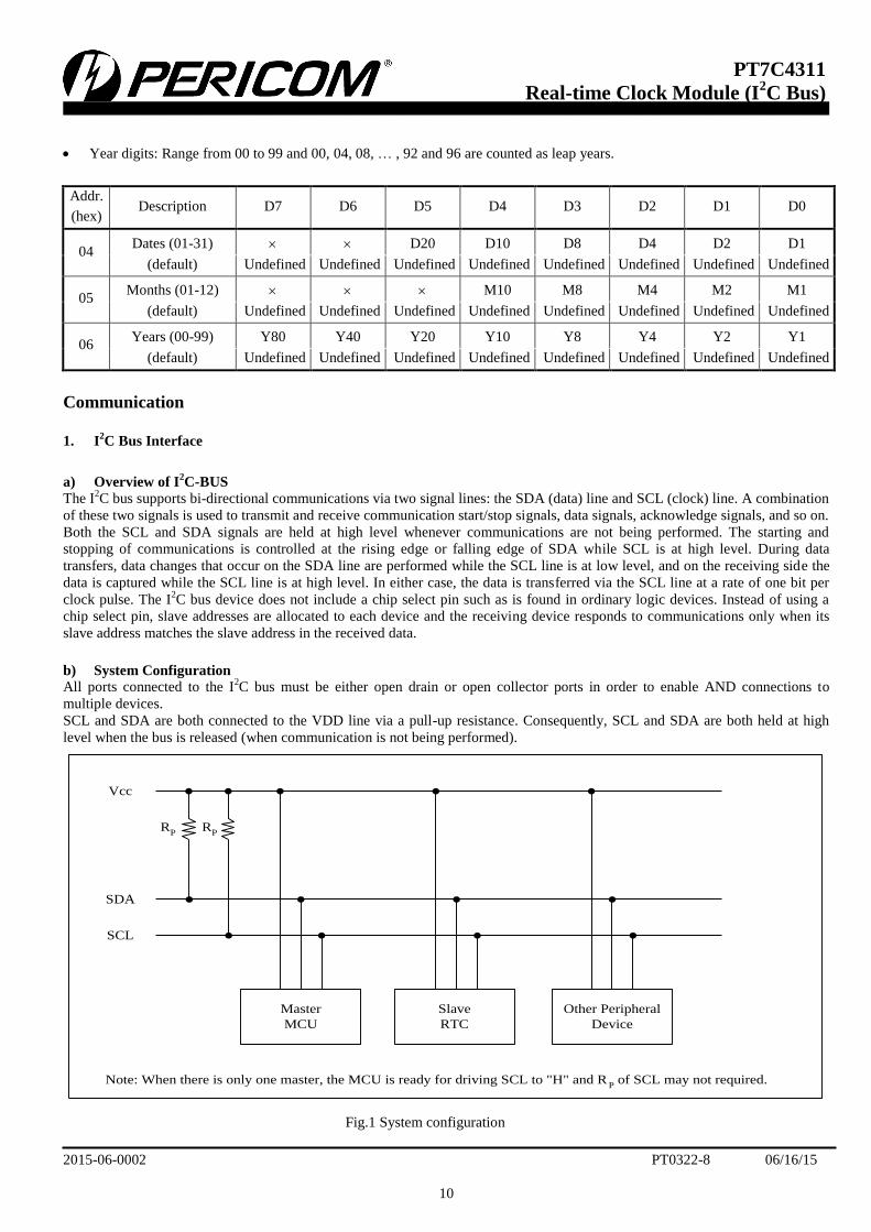
Communication
1. I
2C Bus Interface
a) Overview of I2C-BUS
The I2C bus supports bi-directional communications via two signal lines: the SDA (data) line and SCL (clock) line. A combination
of these two signals is used to transmit and receive communication start/stop signals, data signals, acknowledge signals, and so on.
Both the SCL and SDA signals are held at high level whenever communications are not being performed. The starting and
stopping of communications is controlled at the rising edge or falling edge of SDA while SCL is at high level. During data
transfers, data changes that occur on the SDA line are performed while the SCL line is at low level, and on the receiving side the
data is captured while the SCL line is at high level. In either case, the data is transferred via the SCL line at a rate of one bit per
clock pulse. The I2C bus device does not include a chip select pin such as is found in ordinary logic devices. Instead of using a
chip select pin, slave addresses are allocated to each device and the receiving device responds to communications only when its
slave address matches the slave address in the received data.
b) System Configuration
All ports connected to the I2C bus must be either open drain or open collector ports in order to enable AND connections to
multiple devices.
SCL and SDA are both connected to the VDD line via a pull-up resistance. Consequently, SCL and SDA are both held at high
level when the bus is released (when communication is not being performed).
Master
MCU
Slave
RTC
Other Peripheral
Device
Vcc
SDA
SCL
Note: When there is only one master, the MCU is ready for driving SCL to "H" and RP of SCL may not required.
RP
RP
Fig.1 System configuration
|||||||||||||||||||||||||||||||||||||||||||||||||||||||||||||||||||||||||||||||||||||||||||||||||||||||||||||||||||||||||||||||||||||||||||||||||||||||||||||||||||||||||||||||||||||||||||||||||||||||||||||||||||||||||||||||||||||||||||||||||||||||||||||||||||||||||||||||||||||||||||||||||||||||||||||||||||||||||||||||||||||||
2015-06-0002 PT0322-8 06/16/15
11
PT7C4311
Real-time Clock Module (I2C Bus)
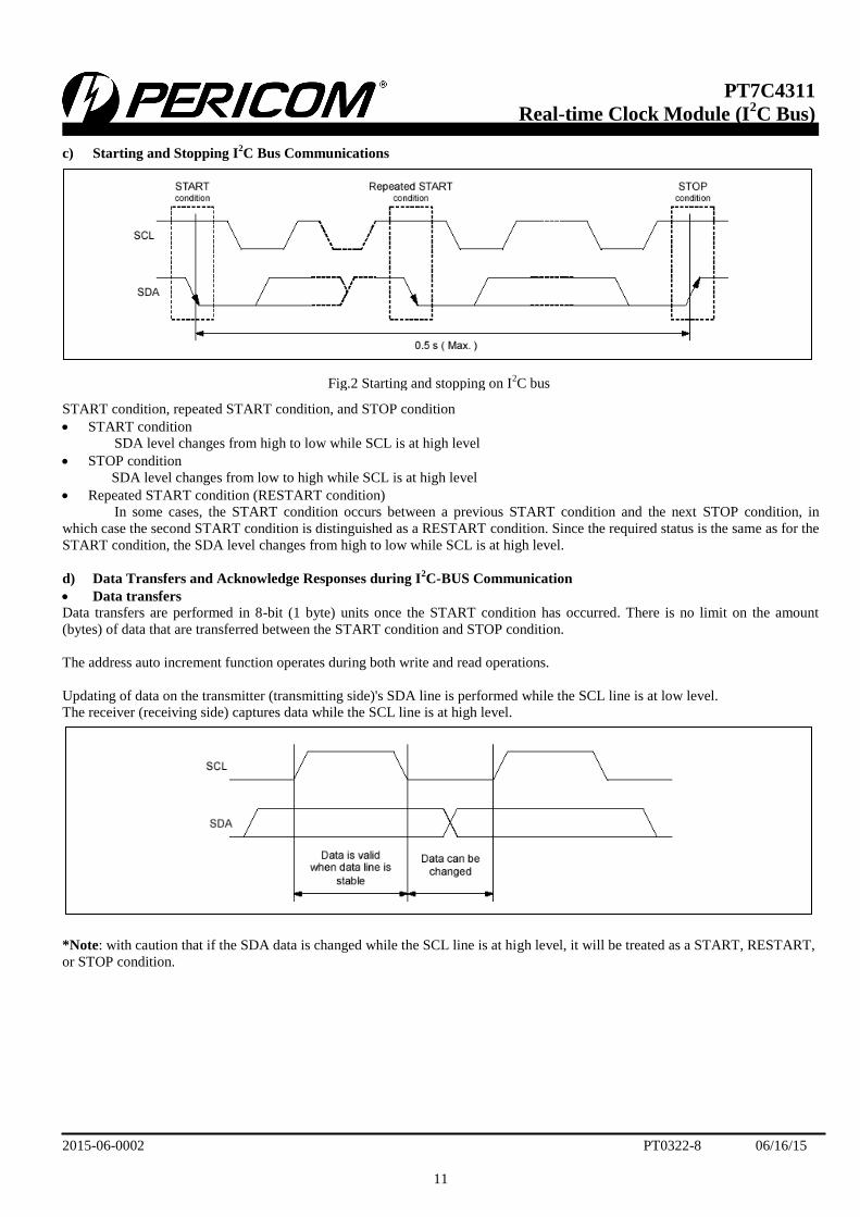
c) Starting and Stopping I2C Bus Communications
START condition, repeated START condition, and STOP condition
START condition
SDA level changes from high to low while SCL is at high level
STOP condition
SDA level changes from low to high while SCL is at high level
Repeated START condition (RESTART condition)
In some cases, the START condition occurs between a previous START condition and the next STOP condition, in
which case the second START condition is distinguished as a RESTART condition. Since the required status is the same as for the
START condition, the SDA level changes from high to low while SCL is at high level.
d) Data Transfers and Acknowledge Responses during I2C-BUS Communication
Data transfers
Data transfers are performed in 8-bit (1 byte) units once the START condition has occurred. There is no limit on the amount
(bytes) of data that are transferred between the START condition and STOP condition.
The address auto increment function operates during both write and read operations.
Updating of data on the transmitter (transmitting side)'s SDA line is performed while the SCL line is at low level.
The receiver (receiving side) captures data while the SCL line is at high level.
*Note: with caution that if the SDA data is changed while the SCL line is at high level, it will be treated as a START, RESTART,
or STOP condition.
Fig.2 Starting and stopping on I2C bus
|||||||||||||||||||||||||||||||||||||||||||||||||||||||||||||||||||||||||||||||||||||||||||||||||||||||||||||||||||||||||||||||||||||||||||||||||||||||||||||||||||||||||||||||||||||||||||||||||||||||||||||||||||||||||||||||||||||||||||||||||||||||||||||||||||||||||||||||||||||||||||||||||||||||||||||||||||||||||||||||||||||||
2015-06-0002 PT0322-8 06/16/15
12
PT7C4311
Real-time Clock Module (I2C Bus)
Data acknowledge response (ACK signal)
When transferring data, the receiver generates a confirmation response (ACK signal, low active) each time an 8-bit data segment
is received. If there is no ACK signal from the receiver, it indicates that normal communication has not been established. (This
does not include instances where the master device intentionally does not generate an ACK signal.)
Immediately after the falling edge of the clock pulse corresponding to the 8th bit of data on the SCL line, the transmitter releases
the SDA line and the receiver sets the SDA line to low (= acknowledge) level.
After transmitting the ACK signal, if the Master remains the receiver for transfer of the next byte, the SDA is released at the
falling edge of the clock corresponding to the 9th bit of data on the SCL line. Data transfer resumes when the Master becomes the
transmitter.
When the Master is the receiver, if the Master does not send an ACK signal in response to the last byte sent from the slave, that
indicates to the transmitter that data transfer has ended. At that point, the transmitter continues to release the SDA and awaits a
STOP condition from the Master.
e) Slave Address
The I2C bus device does not include a chip select pin such as is found in ordinary logic devices. Instead of using a chip select pin,
slave addresses are allocated to each device.
All communications begin with transmitting the [START condition] + [slave address (+ R/W specification)]. The receiving device
responds to this communication only when the specified slave address it has received matches its own slave address.
Slave addresses have a fixed length of 7 bits. See table for the details.
An R/W bit is added to each 7-bit slave address during 8-bit transfers.
Operation Transfer data Slave address
R / W bit
bit 7 bit 6 bit 5 bit 4 bit 3 bit 2 bit 1 bit 0
Read D1 h 1 1 0 1 0 0 0
1 (= Read)
Write D0 h 0 (= Write)
2. I2C Bus’s Basic Transfer Format
SCL from Master 1 2 8 9
SDA from transmitter
(sending side)
SDA from receiver
(receiving side)
Release SDA
Low active
ACK signal
S Start indication P Stop indication
Sr Restart indication
A RTC Acknowledge
A Master Acknowledge
|||||||||||||||||||||||||||||||||||||||||||||||||||||||||||||||||||||||||||||||||||||||||||||||||||||||||||||||||||||||||||||||||||||||||||||||||||||||||||||||||||||||||||||||||||||||||||||||||||||||||||||||||||||||||||||||||||||||||||||||||||||||||||||||||||||||||||||||||||||||||||||||||||||||||||||||||||||||||||||||||||||||
2015-06-0002 PT0322-8 06/16/15
13
PT7C4311
Real-time Clock Module (I2C Bus)
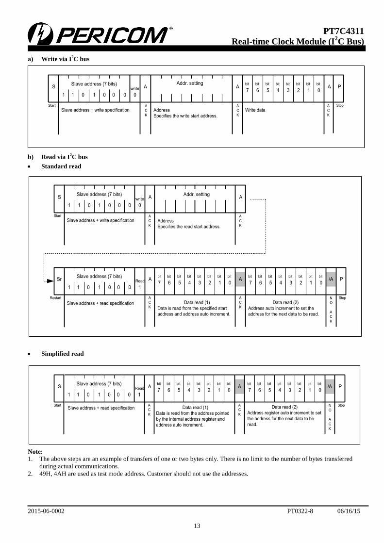
a) Write via I2C bus
b) Read via I2C bus
Standard read
Simplified read
Note: 1. The above steps are an example of transfers of one or two bytes only. There is no limit to the number of bytes transferred
during actual communications.
2. 49H, 4AH are used as test mode address. Customer should not use the addresses.
Slave address (7 bits)
1 1 0 1 0 0 0 0
writeAddr. setting
Slave address + write specification Address
Specifies the write start address.
Abit
7 6 5 4 3 2 1 0
bit bit bit bit bit bit bitA P
Write data
S A
A
C
K
A
C
K
A
C
K
Start Stop
Slave address (7 bits)
1 1 0 1 0 0 0 0
write
Slave address + write specification Address
Specifies the read start address.
Addr. settingAS
Slave address (7 bits)
1 1 0 1 0 0 0 1
Read
Slave address + read specification Data read (1)
Data is read from the specified start
address and address auto increment.
Abit
7 6 5 4 3 2 1 0
bit bit bit bit bit bit bit/A PSr
7 6 5 4 3 2 1 0
bit bit bit bit bit bit bitbit
Data read (2)
Address auto increment to set the
address for the next data to be read.
A
C
K
N
O
A
C
K
A
A
C
K
A
C
K
A
C
K
A
Start
StopRestart
Data read (2)
Address register auto increment to set
the address for the next data to be
read.
Data read (1)
Data is read from the address pointed
by the internal address register and
address auto increment.
Slave address (7 bits)
1 1 0 1 0 0 0 1
Read Abit
7 6 5 4 3 2 1 0
bit bit bit bit bit bit bit/A PS
7 6 5 4 3 2 1 0
bit bit bit bit bit bit bitbit
A
C
K
N
O
A
C
K
A
C
K
A
StopStartSlave address + read specification
|||||||||||||||||||||||||||||||||||||||||||||||||||||||||||||||||||||||||||||||||||||||||||||||||||||||||||||||||||||||||||||||||||||||||||||||||||||||||||||||||||||||||||||||||||||||||||||||||||||||||||||||||||||||||||||||||||||||||||||||||||||||||||||||||||||||||||||||||||||||||||||||||||||||||||||||||||||||||||||||||||||||
2015-06-0002 PT0322-8 06/16/15
14
PT7C4311
Real-time Clock Module (I2C Bus)
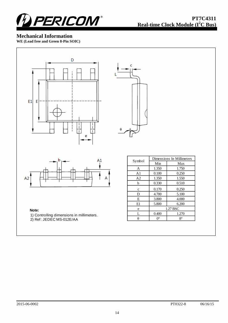
Mechanical Information WE (Lead free and Green 8-Pin SOIC)
Min Max
A 1.350 1.750
A1 0.100 0.250
A2 1.350 1.550
b 0.330 0.510
c 0.170 0.250
D 4.700 5.100
E 3.800 4.000
E1 5.800 6.200
e
L 0.400 1.270
θ 0° 8°
SymbolDimensions In Millimeters
1.27 BSCNote:
1) Controlling dimensions in millimeters.2) Ref : JEDEC MS-012E/AA

|||||||||||||||||||||||||||||||||||||||||||||||||||||||||||||||||||||||||||||||||||||||||||||||||||||||||||||||||||||||||||||||||||||||||||||||||||||||||||||||||||||||||||||||||||||||||||||||||||||||||||||||||||||||||||||||||||||||||||||||||||||||||||||||||||||||||||||||||||||||||||||||||||||||||||||||||||||||||||||||||||||||
2015-06-0002 PT0322-8 06/16/15
15
PT7C4311
Real-time Clock Module (I2C Bus)
ZEE (Lead free and Green 8-Pin TDFN)
SYMBOL MIN. MAXA 0.700 0.800A1 0.000 0.500A3D 1.924 2.076E 2.924 3.076D1 1.400 1.600E1 1.400 1.600kb 0.200 0.300eL 0.224 0.376
PKG. DIMENSIONS(MM)
0.203REF
0.200MIN
0.500TYP
Note:
Ref: JEDEC MO-229
|||||||||||||||||||||||||||||||||||||||||||||||||||||||||||||||||||||||||||||||||||||||||||||||||||||||||||||||||||||||||||||||||||||||||||||||||||||||||||||||||||||||||||||||||||||||||||||||||||||||||||||||||||||||||||||||||||||||||||||||||||||||||||||||||||||||||||||||||||||||||||||||||||||||||||||||||||||||||||||||||||||||
2015-06-0002 PT0322-8 06/16/15
16
PT7C4311
Real-time Clock Module (I2C Bus)
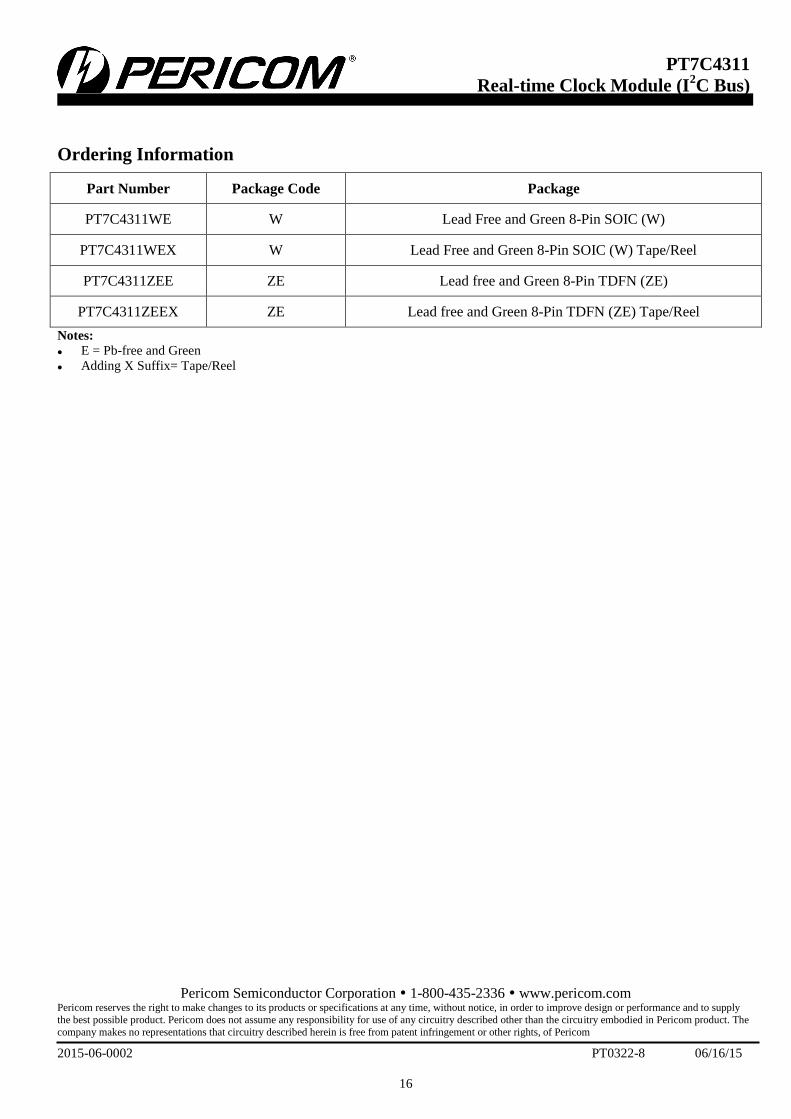
Ordering Information
Part Number Package Code Package
PT7C4311WE W Lead Free and Green 8-Pin SOIC (W)
PT7C4311WEX W Lead Free and Green 8-Pin SOIC (W) Tape/Reel
PT7C4311ZEE ZE Lead free and Green 8-Pin TDFN (ZE)
PT7C4311ZEEX ZE Lead free and Green 8-Pin TDFN (ZE) Tape/Reel
Notes:
E = Pb-free and Green
Adding X Suffix= Tape/Reel
Pericom Semiconductor Corporation 1-800-435-2336 www.pericom.com Pericom reserves the right to make changes to its products or specifications at any time, without notice, in order to improve design or performance and to supply
the best possible product. Pericom does not assume any responsibility for use of any circuitry described other than the circuitry embodied in Pericom product. The
company makes no representations that circuitry described herein is free from patent infringement or other rights, of Pericom