circuit theory 2nd year elect. ﺔ 0b 9/2010 · page 1 of 4 - ﺔﻴﺟﺫﻮﻤﻧ ﺔﺑﺎﺟﺇ...
TRANSCRIPT

Page 1 of 4 - إجابة نموذجية ASSIUT UNIVERSITY FACULTY OF ENGINEERING DEPT. OF ELECTRICAL ENG.
CIRCUIT THEORY 2BFirst Term Examination, 2009/2010
2nd Year Elect. 0B ۱۹۹۷ ،۲۰۰٤ ةالئح(جميع الطلبة(
1BTime: 3 Hours .درجة ۱۰۰االمتحان مكون من أربع صفحات، اإلجابة فى نفس ورقة األسئلة، النهاية العظمى
.اإلجابة النهائية يجب أن تكون مكتوبة فى المكان المخصص لها ولن يلتفت لغير ذلكQuestion 1: a) The op-amp in the circuit of Fig.a is ideal. Calculate the following: (10 Marks)
b) The switch in the circuit of Fig. (b) has been in position a for a long time. At t=0 it moves to position b. Calculate the following: (10 Marks)
c) The circuit of Fig. (c) operates at radian frequency ω = 100 rad/sec. Find the
mutual inductance M, the reflected impedance Zr and the input impedance at port a-b. (6 Marks)
-
+
Vo
Fig. (a)
3KΩ 3 KΩ
1 V + _
2 KΩ
I3
I1
I2
1 KΩ
0.2 V + _
2 KΩ I4
I1 0.4 mA
I2
0
I3
0.5 mA
I4
0.9 mA
Vo - 3.7 V
+
_ 28V
Fig. (b)
+
_ 20V
+
_ vo(t)
24KΩ
0.2H b t=0 12KΩ a
4KΩ
8nF +
_ vC(t)
iL(t)
iC(t)
vC(0+) 26 V
iL(0+) 0.5 mA
vo(0-) 20 V
vo(0+) 22 V
ic(0+) - 0.5 mA
100µF
Fig. (c)
4H
b
300 Ω
a
1H
k=0.75
Zin 154.4∠30.3°Ω
Zr 27-j36 = 45∠-53.1°Ω
M 1.5 H
Page 2 of 4 - إجابة نموذجية
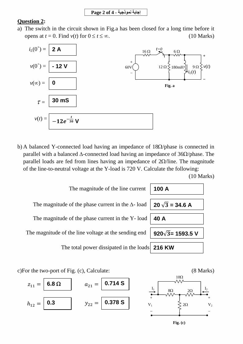
Question 2: a) The switch in the circuit shown in Fig.a has been closed for a long time before it
opens at t = 0. Find v(t) for 0 ≤ t ≤ ∞. (10 Marks)
b) A balanced Y-connected load having an impedance of 18Ω/phase is connected in
parallel with a balanced ∆-connected load having an impedance of 36Ω/phase. The parallel loads are fed from lines having an impedance of 2Ω/line. The magnitude of the line-to-neutral voltage at the Y-load is 720 V. Calculate the following:
(10 Marks)
c)For the two-port of Fig. (c), Calculate: (8 Marks)
IAB
v(0+) =
τ =
v(∞) =
v(t) =
The magnitude of the line current
100 A
𝑎21 =
iL(0+) =
+
_ 60V
Fig. a
9 Ω v(t)
t=0 6 Ω
180mH
16 Ω
12 Ω
+
_ iL(t)
The total power dissipated in the loads 216 KW
The magnitude of the phase current in the ∆- load
20 √𝟑 = 34.6 A
The magnitude of the phase current in the Y- load
40 A
The magnitude of the line voltage at the sending end
920√𝟑= 1593.5 V
2Ω 8Ω
Fig. (c)
2Ω
I1 I2
+
_ V1
+
_ V2
10Ω
𝑧11 =
ℎ12 = 𝑦22 =
2 A
- 12 V
0
30 mS
−𝟏𝟐𝒆−𝒕𝟑𝟎 V
6.8 Ω
0.3 0.378 S
0.714 S
Page 3 of 4 - إجابة نموذجية
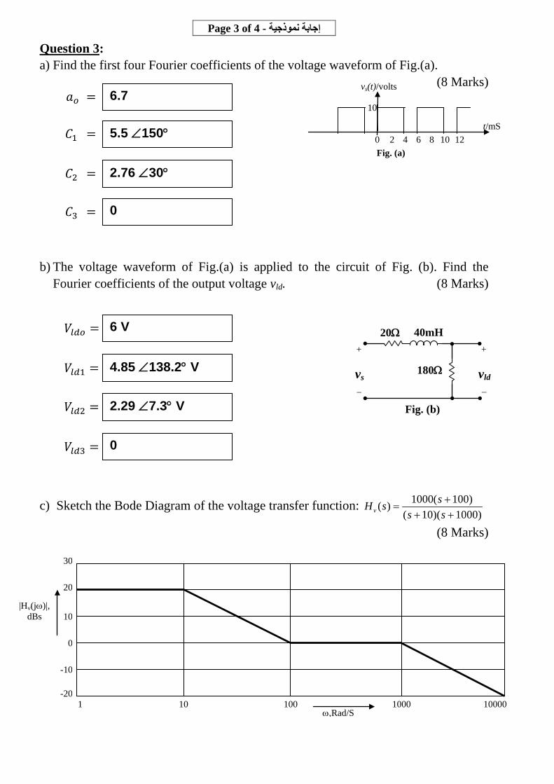
Question 3: a) Find the first four Fourier coefficients of the voltage waveform of Fig.(a). (8 Marks) b) The voltage waveform of Fig.(a) is applied to the circuit of Fig. (b). Find the
Fourier coefficients of the output voltage vld. (8 Marks) c) Sketch the Bode Diagram of the voltage transfer function:
)1000)(10()100(1000)(
+++
=ss
ssHv
(8 Marks)
1 10 100 1000 10000 ω,Rad/S
30
20
10
0
-10
-20
|Hv(jω)|, dBs
t/mS
vs(t)/volts
Fig. (a)
10
0 2 4 6 8 10 12
40mH
+
_ vld
Fig. (b)
180Ω
20Ω +
_ vs
𝑎𝑜 =
𝐶2 =
𝐶3 =
𝑉𝑙𝑑𝑜 =
𝑉𝑙𝑑2 =
𝑉𝑙𝑑3 =
6.7
𝐶1 = 5.5 ∠150°
2.76 ∠30°
0
6 V
4.85 ∠138.2° V
2.29 ∠7.3° V
0
𝑉𝑙𝑑1 =

Page 4 of 4 - إجابة نموذجية
Question 4: a) Find the voltage transfer function and its poles
and zeros for the circuit of Fig.a. (10 Marks)
b) The switch in the circuit shown in Fig.b has been opened for a long time before it closes at t = 0. Find vc(t) for t ≥ 0. (12 Marks)
******************** أطيب التمنيات بالتوفيق********************
مجدى مفيد دوس. د.أ
𝑯𝒗(𝒔) =𝟏𝟎𝟒
𝒔𝟐 + 𝟏𝟎𝟎𝒔 + 𝟏𝟎𝟒
Poles: -50 + j 86.6, -50 - j 86.6 Zeros: ∞, ∞
𝑽𝑪(𝒔) =𝟏𝟐𝟎
𝒔(𝒔𝟐 + 𝟒𝒔 + 𝟑)
𝒗𝑪(𝒕) = [𝟒𝟎 − 𝟔𝟎𝒆−𝒕 + 𝟐𝟎𝒆−𝟑𝒕]𝒖(𝒕) 𝑽
= 𝟏𝟐𝟎𝒔(𝒔+𝟏)(𝒔+𝟑)
= 𝟒𝟎
𝒔− 𝟔𝟎
𝒔+𝟏+ 𝟐𝟎
𝒔+𝟑
V=40 V
1H
1/3 F
+
_ vc
4Ω
Fig. (b)
+
_
t=0
Vin
+
_
Vout
1H
100µF 100Ω
Fig.(a)
+
_

Model Answer-Page 1 of 4 ASSIUT UNIVERSITY FACULTY OF ENGINEERING DEPT. OF ELECTRICAL ENG.
E222 CIRCUIT THEORY First Term Examination, 2010/2011
2nd Year Elect. 0B ۱۹۹۷ ،۲۰۰٤ ةالئح(جميع الطلبة(
1BTime: 3 Hours .درجة ۱۰۰ االمتحان مكون من أربع صفحات، اإلجابة فى نفس ورقة األسئلة، النهاية العظمى
.اإلجابة النهائية يجب أن تكون مكتوبة فى المكان المخصص لها ولن يلتفت لغير ذلكQuestion 1: a) The voltage waveform vg shown in
Fig.(a-1) is applied to the circuit of Fig.(a-2). Sketch vo and v1 versus t, assuming ideal op-amp. (10 Marks)
b) The switch in the circuit shown in Fig.b has been opened for a long time before it
closes at t = 0. Find io(t) for 0 ≤ t ≤ ∞. (10 Marks)
io(0+) =
τ =
io(∞) =
io(t) =
iL(0+) =
+
_ 90V
Fig. b
t=0
20 Ω
10 H
30 Ω
60 Ω iL(t)
io(t)
20 Ω
-
+
vo
Fig. (a-2)
28 KΩ
vg + _
2 KΩ
v1
+10V
-8V
Fig. (a-1)
t/mS
vg(t)/volts
1.0
0 2 4 6 8 10 12
1.5
0.5
-1.0 -0.5
-1.5
t/mS
vo(t)/volts
10
0 2 4 6 8 10 12
15
5
-10 -5
-15
t/mS
v1(t)/volts
0.4
0 2 4 6 8 10 12
0.6
0.2
-0.4 -0.2
-0.6
-0.27
1 A
0.5 A
1.5 A
0.5 S
1.5 - e-2t A, 0 ≤ t ≤ ∞
Model Answer-Page 2 of 4
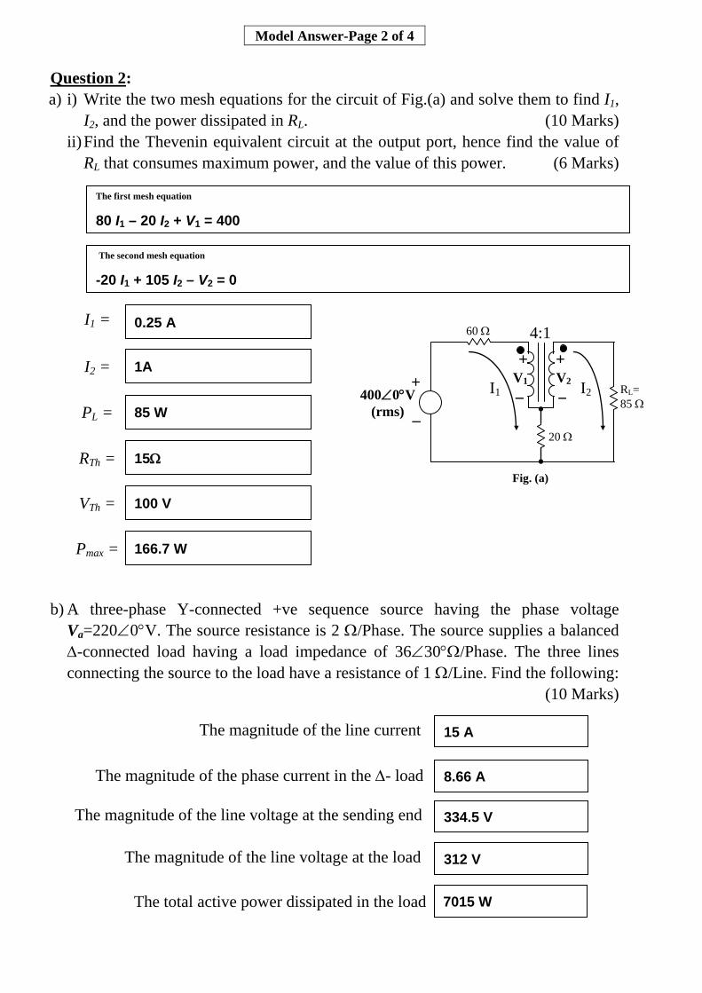
Question 2: a) i) Write the two mesh equations for the circuit of Fig.(a) and solve them to find I1,
I2, and the power dissipated in RL. (10 Marks) ii) Find the Thevenin equivalent circuit at the output port, hence find the value of
RL that consumes maximum power, and the value of this power. (6 Marks) b) A three-phase Y-connected +ve sequence source having the phase voltage
Va=220∠0°V. The source resistance is 2 Ω/Phase. The source supplies a balanced ∆-connected load having a load impedance of 36∠30°Ω/Phase. The three lines connecting the source to the load have a resistance of 1 Ω/Line. Find the following:
(10 Marks)
PL = 85 W
RTh = 15Ω
VTh = 100 V
IAB The magnitude of the line current
15 A
The magnitude of the phase current in the ∆- load
8.66 A
The first mesh equation 80 I1 – 20 I2 + V1 = 400
The second mesh equation -20 I1 + 105 I2 – V2 = 0
I2 = 1A
I1 = 0.25 A
Pmax = 166.7 W
The total active power dissipated in the load 7015 W
The magnitude of the line voltage at the sending end
334.5 V
The magnitude of the line voltage at the load
312 V
Fig. (a)
_ RL= 85 Ω
+
4:1
400∠0°V (rms)
20 Ω
60 Ω
I1 I2
+ +
_ _ V1 V2
Model Answer-Page 3 of 4
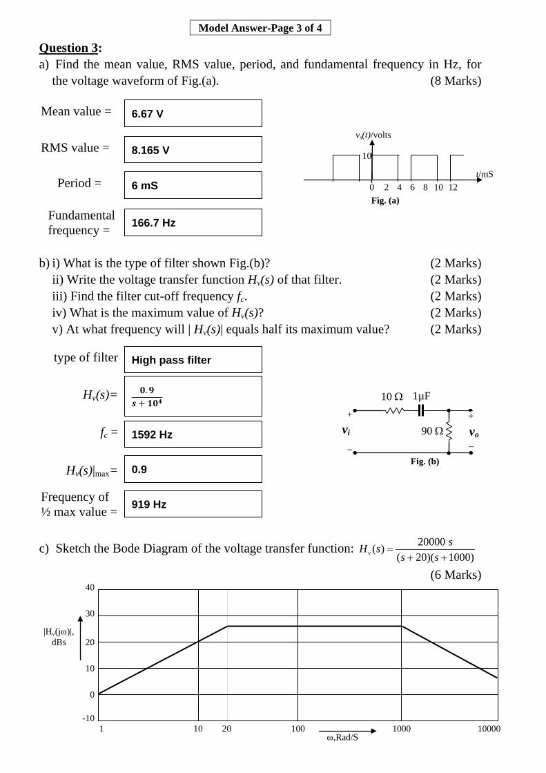
Question 3: a) Find the mean value, RMS value, period, and fundamental frequency in Hz, for
the voltage waveform of Fig.(a). (8 Marks) b) i) What is the type of filter shown Fig.(b)? (2 Marks) ii) Write the voltage transfer function Hv(s) of that filter. (2 Marks) iii) Find the filter cut-off frequency fc. (2 Marks) iv) What is the maximum value of Hv(s)? (2 Marks) v) At what frequency will | Hv(s)| equals half its maximum value? (2 Marks) c) Sketch the Bode Diagram of the voltage transfer function:
)1000)(20(20000)(
++=
ssssHv
(6 Marks)
1 10 100 1000 10000 ω,Rad/S
40
30
20
10
0
-10
|Hv(jω)|, dBs
t/mS
vs(t)/volts
Fig. (a)
10
0 2 4 6 8 10 12
Mean value =
RMS value =
Period =
Fundamental frequency =
type of filter
Hv(s)=
fc =
Hv(s)|max=
Frequency of ½ max value =
vi
1µF 10 Ω
Fig. (b)
+
_
+
_ vo 90 Ω
6.67 V
8.165 V
6 mS
166.7 Hz
High pass filter
𝟎.𝟗𝒔 + 𝟏𝟎𝟒
1592 Hz
0.9
919 Hz
20

Model Answer-Page 4 of 4
Question 4: a) Find the s-domain expression of the input impedance seen
looking into the terminals a, b of the circuit of Fig.(a). Find also the poles and zeros of that impedance. (10 Marks)
b) The switch in the circuit of Fig. (b) is
moved from (a) to (b) at t = 0. Find the following currents and voltages:
(12 Marks) c) The a-parameters of a certain two-port are a11= 3, a12= 10 Ω, a21= 0.5 S, a22= 2.
Find the h-parameters. (8 Marks)
******************** التمنيات بالتوفيق أطيب******************** مجدى مفيد دوس. د.أ
ℎ12 = ℎ11 =
ℎ21 = ℎ22 =
1H 1F 1Ω
Fig.(a)
a
b
1F 1Ω
Zin(s) =
𝟐𝐬𝟐 + 𝟑𝐬 + 𝟏𝟐𝐬(𝐬𝟐 + 𝐬 + 𝟏)
Poles
0, (-0.5 + j 0.866), (-0.5 - j 0.866)
Zeros
-0.5, -1, ∞
+
_ 10V
Fig. (b)
+
_ 5V
+
_ vR
+
_ vC 5 Ω
5 Ω
iC iR
iL + _ vL t=0
(a) (b)
iR(0-) 2 A
ic(0+)
1 A
iL(0+)
2 A
vL (0+)
5 V
vR(∞) 10 V
iR(0+) 1 A
5 Ω
0.5 0.25 S
-0.5

إجابة نموذجية Page 1 of 4
ASSIUT UNIVERSITY FACULTY OF ENGINEERING DEPT. OF ELECTRICAL ENG.
E222 CIRCUIT THEORY 2BFirst Term Examination, 2011/2012
2 Und U Year Elect. 0B ۲۰۰٤،۱۹۹۷الئحة (جميع الطلبة(
1BTime: 3 Hours
.درجة ۱۰۰العظمى االمتحان مكون من أربع صفحات، اإلجابة فى نفس ورقة األسئلة، النهاية
.اإلجابة النهائية يجب أن تكون مكتوبة فى المكان المخصص لها ولن يلتفت لغير ذلك
Question 1: a) The op-amp in the non-inverting amplifier of Fig.a is ideal. Find the i1, i2, v1, i3, vo,
and io. (12 Marks)
b) The switch in the circuit shown in Fig.b has been in
position (a) for a long time before it moves to (b) at t = 0. After 5 mSec, the inductance current iL dropped to 80% of its initial value. Find the value of L.
(12 Marks)
i1 = 0.1 mA
i2 = 0.2 mA
v1= 4 V
vo = 8 V
i3 = 0.2 mA
40KΩ
Fig.a
2V + _
-
+
20KΩ +15 V
-15 V
vo
10V + _
5V + _
10KΩ
10KΩ
4KΩ
20KΩ
20KΩ
v1 io
i1
i2
i3
io = 0.4 mA
+
_ 30V
Fig. b
t=0 60 Ω
L iL(t)
40 Ω (a) (b)
+
_ 10V
𝒊(𝒕) = 𝟎.𝟐𝟓 + 𝟎.𝟐𝟓𝒆−𝒕/𝝉
𝒊(𝟓𝐦𝐒) = 𝟎.𝟐𝟓𝟏 + 𝒆−𝟓𝝉 = 𝟎.𝟒 𝐀
iL(0+) = iL(∞) =
τ =
L =
0.5 A
0.25 A
9.788 mS
392 mH

إجابة نموذجية Page 2 of 4 Question 2: a) A three-phase ∆-connected +ve sequence source having the phase voltage
Vab=220∠0°V. The source resistance is 1 Ω / Phase. The source supplies an unbalanced ∆-connected resistive load having Rab = 10Ω, Rbc = 9Ω and Rca = 21Ω. The three lines connecting the source to the load have negligible resistance. The load power is measured using the two wattmeter method. The first wattmeter W1 is connected between lines A and B, while the second one W2 is connected between lines C and B. Find the following: (12 Marks)
The phase current at the load =
The Line current =
The line voltage at the load =
The reading of W1 =
The reading of W2 = The total power dissipated in the load =
b) i) Find the voltage transfer function of the
circuit of Fig.(b). (6 Marks) ii) Find the poles and zeros of the transfer
function. (4 Marks) iii) Find the magnitude of the transfer function at
ω = 5 Rad/Sec. (2 Marks)
IAB
IA
VAB
20∠0° A
26.46∠-19.1° A
200∠0° V
5 KW
5.35 KW
10.35 KW
Poles: - 4.23 , - 15.77 S-1
Zeros: 0, ∞
|Hv(j5)| = 0.308
𝑯𝒗(𝒔) =𝟐𝟎𝒔
𝟑𝒔𝟐 + 𝟔𝟎𝒔 + 𝟐𝟎𝟎
(2s + 10)I1 + s I2 = 2 V1 S I1 + (2s + 20)I2 = 0
5 Ω 0.5 H
1 H
Fig. (b)
+
_ V1
+
_ V2 1 H 10Ω
إجابة نموذجية Page 3 of 4
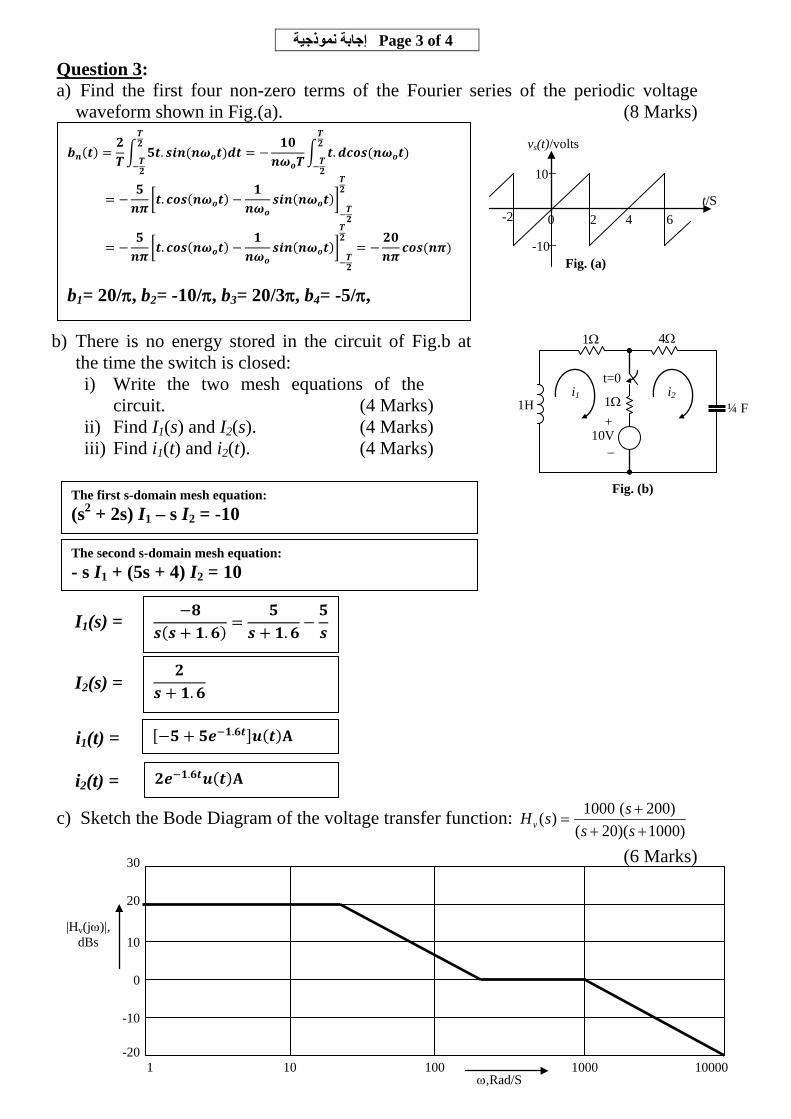
Question 3: a) Find the first four non-zero terms of the Fourier series of the periodic voltage
waveform shown in Fig.(a). (8 Marks)
b) There is no energy stored in the circuit of Fig.b at the time the switch is closed: i) Write the two mesh equations of the
circuit. (4 Marks) ii) Find I1(s) and I2(s). (4 Marks) iii) Find i1(t) and i2(t). (4 Marks)
c) Sketch the Bode Diagram of the voltage transfer function: )1000)(20(
)200(1000)(+++
=ssssHv
(6 Marks)
1 10 100 1000 10000 ω,Rad/S
30
20
10
0
-10
-20
|Hv(jω)|, dBs
¼ F
Fig. (b)
4Ω 1Ω
t=0
1H
10V
+
_
1Ω i1 i2
The first s-domain mesh equation: (s2 + 2s) I1 – s I2 = -10
The second s-domain mesh equation: - s I1 + (5s + 4) I2 = 10
𝒃𝒏(𝒕) =𝟐𝑻 𝟓𝒕. 𝒔𝒊𝒏(𝒏𝝎𝒐𝒕)𝒅𝒕𝑻𝟐
−𝑻𝟐
= −𝟏𝟎
𝒏𝝎𝒐𝑻 𝒕.𝒅𝒄𝒐𝒔(𝒏𝝎𝒐𝒕)𝑻𝟐
−𝑻𝟐
= −𝟓𝒏𝝅
𝒕. 𝒄𝒐𝒔(𝒏𝝎𝒐𝒕) −𝟏
𝒏𝝎𝒐𝒔𝒊𝒏(𝒏𝝎𝒐𝒕)
−𝑻𝟐
𝑻𝟐
= −𝟓𝒏𝝅
𝒕. 𝒄𝒐𝒔(𝒏𝝎𝒐𝒕) −𝟏
𝒏𝝎𝒐𝒔𝒊𝒏(𝒏𝝎𝒐𝒕)
−𝑻𝟐
𝑻𝟐
= −𝟐𝟎𝒏𝝅
𝒄𝒐𝒔(𝒏𝝅)
b1= 20/π, b2= -10/π, b3= 20/3π, b4= -5/π,
t/S
vs(t)/volts
Fig. (a)
10
0 -2 2 4 6
-10
𝟐𝒔 + 𝟏.𝟔
I2(s) =
−𝟖𝒔(𝒔 + 𝟏.𝟔) =
𝟓𝒔 + 𝟏.𝟔
−𝟓𝒔
I1(s) =
𝟐𝒆−𝟏.𝟔𝒕𝒖(𝒕)𝐀 i2(t) =
[−𝟓 + 𝟓𝒆−𝟏.𝟔𝒕]𝒖(𝒕)𝐀 i1(t) =

إجابة نموذجية Page 4 of 4
Question 4: a) The switch in the circuit of Fig. (a) has been open a
long time before closing at t = 0. i) Find iL(0+), iL(∞), vL(0+), 𝑑𝑖𝐿
𝑑𝑡(0+). (8 Marks)
ii) Write the differential equation of iL(t). (2 Marks) iii) Write the characteristic equation and find its
roots. (4 Marks) iv) The constants in the solution for iL(t). (2 Marks) v) Find iL(t) for t ≥ 0. (2 Marks)
b) Find the h parameters of the circuit shown in
Fig.(b). (8 Marks)
******************** أطيب التمنيات بالتوفيق******************** مجدى مفيد دوس. د.أ
ℎ12 = ℎ11 =
ℎ21 = ℎ22 =
iL(0+) 0
iL(∞) 2 A
+
_ 40V
Fig. (a)
20 Ω iL t=0
500 µF 0.8H
𝒅𝒊𝑳𝒅𝒕
(𝟎+) 𝑽𝑳(𝟎+)𝑳
= 𝟓𝟎 𝐀/𝐒
𝒅𝟐𝒊𝒅𝒕𝟐
+𝟏𝑹𝑪
.𝒅𝒊𝒅𝒕
+𝟏𝑳𝑪
. 𝒊 =𝟐𝑳𝑪
the differential equation of iL(t)
the characteristic equation
s2 + 100 s + 2500 = 0
roots of the characteristic equation s1 = s2 = -50
The constants D1 = -50, D2 = -2
iL(t) = 2 – (50 t + 2) e-50t
Fig.(b)
I2
45Ω
+ -
90Ω 30 Ia
+
_
V1
30Ω
80Ω
I1
+
_
V2 Ia
60 Ω 0.333
8.8 mS -0.21
vL(0+) 40 V

Model Answer-Page 1 of 4
ASSIUT UNIVERSITY FACULTY OF ENGINEERING DEPT. OF ELECTRICAL ENG.
E222 CIRCUIT THEORY First Term Examination, 2012/2013
2nd Year Elect.
Time: 3 Hours
.درجة ۱۰۰االمتحان مكون من أربع صفحات، اإلجابة فى نفس ورقة األسئلة، النهاية العظمى
.وخطوات الحل تكون فى الصفحة المقابلةاإلجابة النهائية يجب أن تكون مكتوبة فى المكان المخصص لها
Question #1: (12 Points) The two op amps in the circuit in Fig.1 are ideal. Calculate vo1, vo2, io1 and io2. Question #2: (16 Points) The voltage waveform shown in Fig.2(a) is applied to the circuit of Fig.2(b). The initial voltage on the capacitor is zero. Calculate and sketch vo(t).
vo1 = 2.125 V
vo2 = 2.5 V
io1= 0.25 mA
Io2 = 1.75 mA
vo(0+) = 0
vo(∞)1 = 10 V
τ = 1 mS
vo(t) = 10(1 – e-t) V 0 <= t <= 1 mS
500Ω
Fig.1
+
-
+15 V
-15 V
vo1
2V io1
+
-
+15 V
-15 V
2KΩ
1KΩ
500Ω
vo2
2KΩ 1V io2
Fig.2(b)
10 KΩ
100 nF
+
_ vo
+
_ vs
Fig.2(a)
10
0
-10
t/mS
vs(t)/volts
2 4 5 1 3 6 7 8
vo(t) = -10 + 16.3 e-(t-1) V 1mS <= t <= ∞
vo(1mS) = 6.3 V
vo(∞) = -10 V
10 8 6 4 2
-2 -4 -6 -8
-10
t/mS
vo(t)/volts
2 4 5 1 3 6 7 8 0
6.3V

Model Answer-Page 2 of 4
Question #3: (10 Points) The voltage response for the circuit in Fig.3 is known to be v(t) = D1te-500t + D2e-500t , t ≥ 0. The initial current in the inductor (Io) is -10 mA, and the initial voltage on the capacitor (Vo) is 8 V. The inductor has an inductance of 4 H. a) Find the values of R, C, D1 and D2. b) Find iC(t) for t ≥ 0+.
Question #4: (12 Points) A three-phase Y-connected +ve sequence source having the phase voltage Va=260∠0°V. The source resistance is 1 Ω/Phase. The source supplies a balanced ∆-connected load having an impedance of (27 + j15) Ω/Phase. The three lines connecting the source to the load have a resistance of 2 Ω/Line. Find the following: The Line current =
The phase current at the load =
The line voltage at the load =
The phase voltage at the source terminals =
The line voltage at the source terminals =
The total power dissipated in the load =
418.6∠31.8° V
Va
IAB
VAB
20∠-22.6° A
11.55∠7.4° A
356.7∠36.4° V
241.7∠1.8° V
IA
Vab
10.8 KW
iC(t) = -3 t e-500t + 2x10⁻³ e-500t A
+
_ Vo
Fig.3
Io C L R
+
_ v
iC
R = 1 KΩ
C = 1 µF
D1 = 6000 V/S
D2 = 8 V

Model Answer-Page 3 of 4
Question #5: (12 Points) The sinusoidal voltage source in the circuit of Fig.5 is operating at a frequency of 200 Krad/s. The coefficient of coupling is adjusted until the peak amplitude of i1 is pure real. a) What is the value of k? b) What is the peak amplitude of i1 if vg = 112 cos(2 x 10⁵ t) V ? Question #6: (12 Points) Find the voltage transfer function and its poles and zeros for the circuit of Fig.6. If we consider this circuit as a bandpass filter, find approximate values for its magnitude transfer function at ω = 0 and at its central frequency. Find also the value of its bandwidth.
𝒊𝟏 =𝒗𝒈
𝟐𝟎𝟎 + 𝒋𝟐𝟎𝟎 + 𝟔𝟒𝒌𝟐(𝟑 − 𝒋𝟒)
Zr = 64 k2(3 - j4)
4 x 64 k2 = 200 k = 0.88
i1(peak) = 0.32 A
104 rad/s BW =
+
_ Vi
Fig.6
1KΩ
0.1µF 1 mH
+
_
Vo Poles: -5 ± j 99.87 Krad/s
Hv(s) = 𝟏𝟎𝟒𝒔𝒔𝟐 + 𝟏𝟎𝟒𝒔 + 𝟏𝟎𝟏𝟎
Zeros: 0, ∞
|Hv(0)| = 0
|Hv(jωo)| = 1
200 Ω k
1 mH
Fig.5
4 mH 12.5 nF
300 Ω
+
_ vg
i1

Model Answer-Page 4 of 4
Question #7: (12 Points) There is no energy stored in the circuit of Fig.7 at the time the current source is energized. Use the Laplace Transform to find the nodal voltages.
Question #8: (6 Points) A periodic voltage having a period of 10π µS is given by the following Fourier series:
𝑣𝑔 = 150∑ 1𝑛
sin 𝑛𝜋2
cos𝑛𝜔𝑜𝑡 V∞𝑛=1,3,5,…
This periodic voltage is applied to the circuit shown in Fig.8. Find the amplitude and phase angle of the first three components of vo. Question #9: (8 Points) Find the s-domain expressions for the a parameters of the two-port circuit shown in Fig.9.
******************** أطيب التمنيات بالتوفيق******************** مجدى مفيد دوس. د.أ
𝒂𝟏𝟐 = 𝒂𝟏𝟏 =
𝒂𝟐𝟏 = 𝒂𝟐𝟐 = Fig.9
- I2
+
_
V1
1 F
4 Ω
I1
+
_
V2
1 H
Eq. (1):
V1(s) =
Eq. (2):
V2(s) =
v1(t) = v2(t) =
1H
4F 0.25Ω
+
_ v1
+
_ v2 4Ω 5u(t) A
Fig.7
+
_ vg
Fig.8
6KΩ
10 mH
+
_
vo
𝒗𝒐 =𝒋𝟐𝒏
𝟔 + 𝒋𝟐𝒏𝒗𝒈
ωo = 2π/T = 200 Krad/s vg = 150 cos ωot - 50 cos 3ωot + 30 cos 5ωot
Vo1 = Vo3 = Vo5 =
(s + 4)V1 – 4 V2 = 20
-V1 + (4s2 + 4s + 1) V2 = 0
𝟐𝟎(𝒔𝟐 + 𝒔 + 𝟎.𝟐𝟓)𝒔(𝒔𝟐 + 𝟓𝒔 + 𝟒.𝟐𝟓)
𝟓𝒔(𝒔𝟐 + 𝟓𝒔 + 𝟒.𝟐𝟓)
1.18 - 16.38e-1.09t + 35.2e-3.91t 1.18 – 1.63e-1.09t + 0.45e-3.91t
47.43∠71.6° V 35.34∠-135° V 25.73∠31° V
𝟏 +𝟏𝟒𝒔
𝒔 +𝟏𝟒
+𝟏𝒔
𝟏𝟒
𝒔𝟒
+ 𝟏

Model Answer Page 1 of 4
ASSIUT UNIVERSITY FACULTY OF ENGINEERING DEPT. OF ELECTRICAL ENG.
E222 CIRCUIT THEORY First Term Examination, 2013/2014
2nd
Year Elect.
.درجة ۱۰۰االمتحان مكون من أربع صفحات، اإلجابة فى نفس ورقة األسئلة، النهاية العظمى .وخطوات الحل تكون فى الصفحة المقابلةمكتوبة فى المكان المخصص لها اإلجابة النهائية يجب أن تكون
UAttempt all questions, full mark: 100 Points U UTime: 3 Hours UQuestion #1 U: (12 Points) The nonlinear device (D) used in the circuit of Fig.1 has a characteristic given by:
id = Ieαvd , where vd > 0 and id > 0. Assuming ideal operational amplifier, and that the nonlinear device is operating with positive values of vd and id,
a) find an expression relating vout to vin. (8 Points) b) if I = 0.5 µA, α = 40 V-1 and R = 1 KΩ, find vout
for vin = 5 V. (4 Points)
UQuestion #2U: (14 Points) The two switches (a) and (b) in the circuit of Fig.2 operate simultaneously. Prior to t=0 switch (a) was open and switch (b) was close for a long time. At t=0, switch (a) is closed and switch (b) is opened.
a) Find vC(0+), iC(0+), vC(∞), iC(∞), and the time constant τ. (10 Points) b) Find vC(t) and iC(t) for t≥0. (4 Points)
UHint U: use the superposition theorem.
vout (for vin = 5 V) = - 230 mV
vC(0+) = 0 vC(∞) = 15 V
vC(t) = 15(1- e-2t) V
Fig.1
-
+
+15 V
-15 V
vout
+ - vd
R
id
vin
D
Fig.2
5 Ω
0.1F
10 Ω
8 Ω +
_ 10V
+
_ vC 1A
t=0
t=0
(a)
(b)
𝒗𝒐𝒖𝒕 = −𝟏∝ 𝐥𝐧
𝒗𝒊𝒏𝑹𝑰
iC(0+) = 3 A iC(∞) = 0 τ = 0.5 S
iC(t) = 3 e-2t A
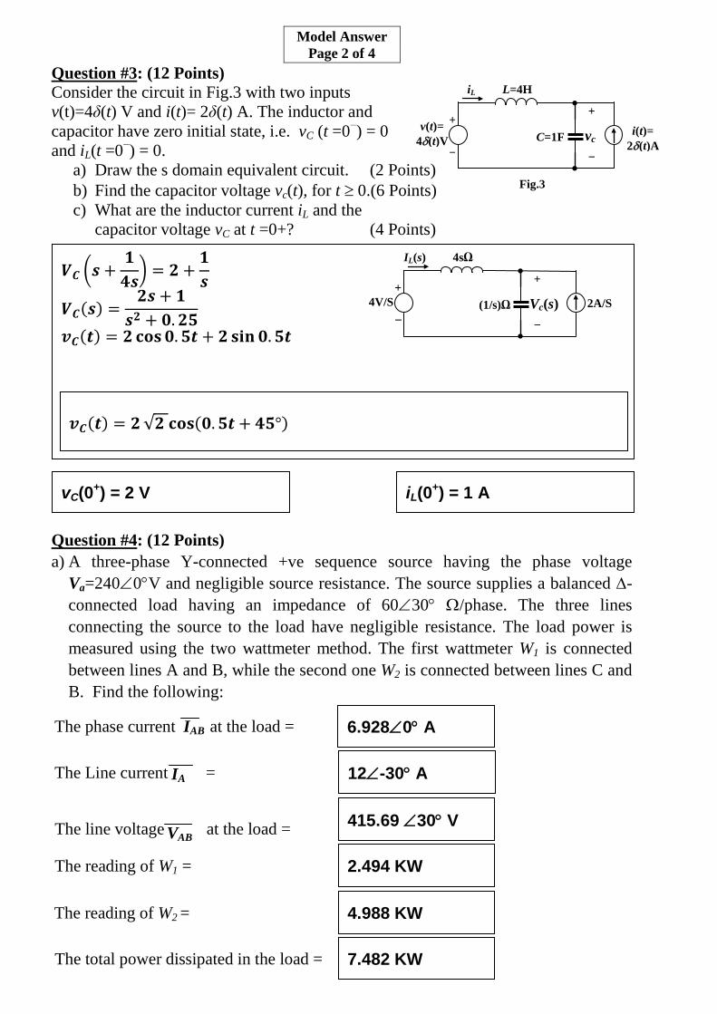
Model Answer Page 2 of 4
Question #3Consider the circuit in Fig.3 with two inputs v(t)=4δ(t) V and i(t)= 2δ(t) A. The inductor and capacitor have zero initial state, i.e. vC (t =0−) = 0 and iL(t =0−) = 0.
: (12 Points)
a) Draw the s domain equivalent circuit. (2 Points) b) Find the capacitor voltage vc(t), for t ≥ 0.(6 Points) c) What are the inductor current iL and the
capacitor voltage vC at t =0+? (4 Points) Question #4a) A three-phase Y-connected +ve sequence source having the phase voltage
Va=240∠0°V and negligible source resistance. The source supplies a balanced ∆-connected load having an impedance of 60∠30° Ω/phase. The three lines connecting the source to the load have negligible resistance. The load power is measured using the two wattmeter method. The first wattmeter W1 is connected between lines A and B, while the second one W2 is connected between lines C and B. Find the following:
: (12 Points)
vC(0+) = 2 V iL(0+) = 1 A
415.69 ∠30° V
Fig.3
C=1F
L=4H
+
_ vc
iL
i(t)= 2δ(t)A
+
_
v(t)= 4δ(t)V
12∠-30° A The Line current = IA
2.494 KW The reading of W1 =
4.988 KW The reading of W2 =
7.482 KW The total power dissipated in the load =
The line voltage at the load = VAB
6.928∠0° A The phase current at the load = IAB
𝑽𝑪 𝒔 +𝟏𝟒𝒔 = 𝟐 +
𝟏𝒔
𝑽𝑪(𝒔) =𝟐𝒔 + 𝟏
𝒔𝟐 + 𝟎.𝟐𝟓
𝒗𝑪(𝒕) = 𝟐 𝐜𝐨𝐬𝟎.𝟓𝒕 + 𝟐 𝐬𝐢𝐧 𝟎.𝟓𝒕
𝒗𝑪(𝒕) = 𝟐√𝟐 𝐜𝐨𝐬(𝟎.𝟓𝒕 + 𝟒𝟓°)
(1/s)Ω
4sΩ IL(s)
2A/S
+
_ 4V/S
+
_ Vc(s)

Model Answer Page 3 of 4
Question #5Consider the circuit of Fig.5, the operational amplifier is ideal. It is required to:
: (14 Points)
a) Find an expression for the voltage transfer function Hv(s) = Vout(s)/Vin(s). (6 points)
b) Compute the numerical values of poles and zeros of the transfer function. (4 points)
c) If the input is a sinusoidal waveform given by: vin(t) = 10 cos(104t + 30°) V; give the expression for the output vout(t). (4 points)
UQuestion #6U: (12 Points) a) A series RLC band-pass filter has
a center, or resonant, frequency of 50 kHz and a quality factor of 4. Find the band-width, the upper cutoff frequency, and the lower cut-off frequency. (6 Points)
b) Use a 5 nF capacitor to design the filter. Draw the circuit diagram and specify the values of R and L. (6 Points)
Poles: - 5 – j 10 Krad/S, - 5 + j 10 Krad/S
Hv(s) = − 𝟏𝑹𝟏𝑪𝟐
𝒔
𝒔𝟐 + 𝟏𝑹𝟐
𝟏𝑪𝟏+ 𝟏𝑪𝟐 𝒔 + 𝟏
𝑹𝟏𝑹𝟐𝑪𝟏𝑪𝟐
=−𝟏.𝟓𝟔𝟐𝟓 × 𝟏𝟎𝟒𝒔
𝒔𝟐 + 𝟏𝟎𝟒𝒔 + 𝟏.𝟐𝟓 × 𝟏𝟎𝟖
Zeros: 0, ∞
Fig.5
-
+
vout
C1 2nF vin
C2 8nF
R2 62.5KΩ
R1 8KΩ
Vout(t) = 15.1585 cos(104t - 135.96°) V
The circuit diagram
C L
+
_ Vo
+
_ Vi
R
BW = 12.5 KHz
R = 159.2 Ω
f1 = 44.14 KHz f2 = 56.64 KHz
L = 2.026 mH
Model Answer Page 4 of 4
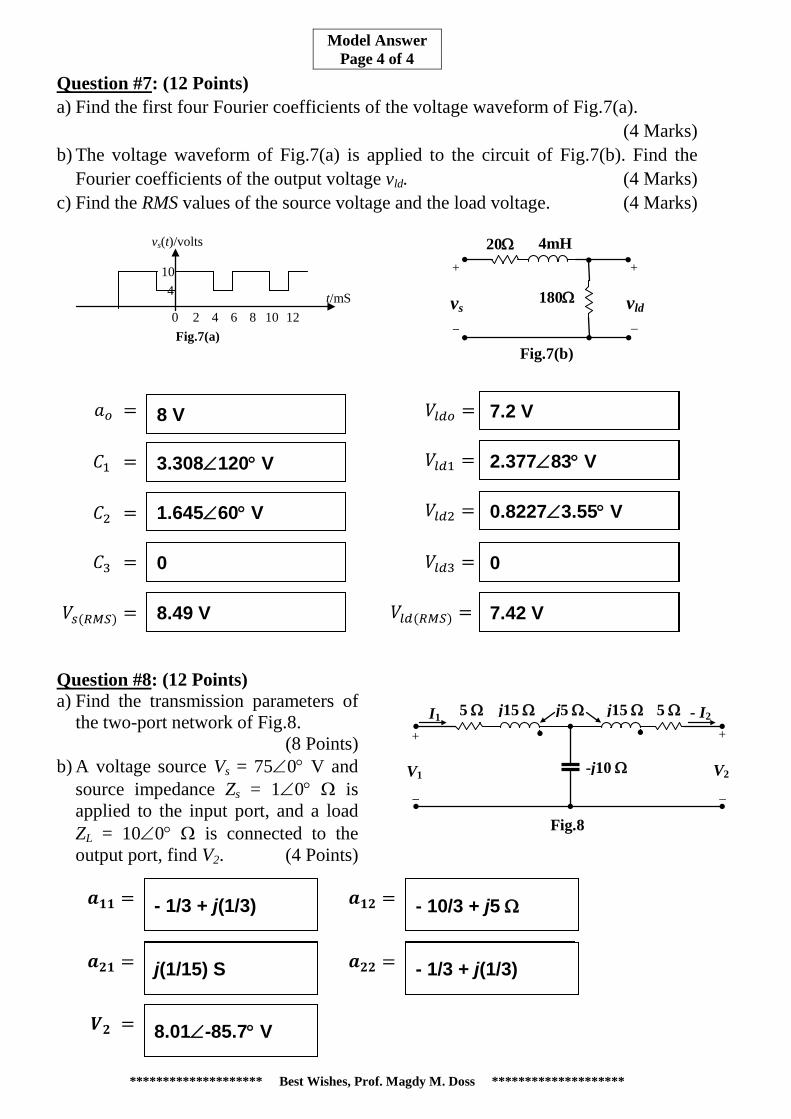
Question #7: (12 Points) a) Find the first four Fourier coefficients of the voltage waveform of Fig.7(a). (4 Marks) b) The voltage waveform of Fig.7(a) is applied to the circuit of Fig.7(b). Find the
Fourier coefficients of the output voltage vld. (4 Marks) c) Find the RMS values of the source voltage and the load voltage. (4 Marks) Question #8: (12 Points) a) Find the transmission parameters of
the two-port network of Fig.8. (8 Points) b) A voltage source Vs = 75∠0° V and
source impedance Zs = 1∠0° Ω is applied to the input port, and a load ZL = 10∠0° Ω is connected to the output port, find V2. (4 Points)
******************** Best Wishes, Prof. Magdy M. Doss ********************
𝒂𝟏𝟐 = 𝒂𝟏𝟏 =
𝒂𝟐𝟏 = 𝒂𝟐𝟐 =
Fig.8
- I2
+
_ V1
5 Ω I1
+
_
V2
5 Ω j15 Ω j15 Ω j5 Ω
-j10 Ω
𝑽𝟐 =
𝐶1 =
𝑎𝑜 =
𝐶2 =
𝐶3 =
𝑉𝑙𝑑1 =
𝑉𝑙𝑑𝑜 =
𝑉𝑙𝑑2 =
𝑉𝑙𝑑3 =
t/mS
vs(t)/volts
Fig.7(a)
10
0 2 4 6 8 10 12
4
𝑉𝑙𝑑(𝑅𝑀𝑆) = 𝑉𝑠(𝑅𝑀𝑆) =
4mH
+
_ vld
Fig.7(b)
180Ω
20Ω +
_ vs
8 V
3.308∠120° V
1.645∠60° V
0
8.49 V 7.42 V
0
0.8227∠3.55° V
2.377∠83° V
7.2 V
- 1/3 + j(1/3)
j(1/15) S
8.01∠-85.7° V
- 10/3 + j5 Ω
- 1/3 + j(1/3)


