christoph adelmann imec, 3001 leuven, belgium abstract
TRANSCRIPT

On the extraction of resistivity and area of nanoscale interconnect
lines by temperature-dependent resistance measurements
Christoph Adelmann∗
Imec, 3001 Leuven, Belgium
Abstract
Several issues concerning the applicability of the temperature coefficient of the resistivity (TCR)
method to scaled interconnect lines are discussed. The central approximation of the TCR method,
i.e. the substitution of the interconnect wire TCR by the bulk TCR becomes doubtful when
the resistivity of the conductor metal is strongly increased by finite size effects. Semiclassical
calculations for thin films show that the TCR deviates from bulk values when the surface roughness
scattering contribution to the total resistivity becomes significant with respect to grain boundary
scattering, an effect that might become even more important in nanowires due to their larger
surface-to-volume ration. In addition, the TCR method is redeveloped to account for line width
roughness. It is shown that for rough wires, the TCR method yields the harmonic average of the
cross-sectional area as well as, to first order, the accurate value of the resistivity at the extracted
area. Finally, the effect of a conductive barrier or liner layer on the TCR method is discussed. It
is shown that the liner or barrier parallel conductance can only be neglected when it is lower than
about 5 to 10% of the total conductance. It is furthermore shown that neglecting the liner/barrier
parallel conductance leads mainly to an overestimation of the cross-sectional area of the center
conductor whereas its resistivity is less affected.
Keywords: Interconnects; resistivity; temperature coefficient of resistivity
∗Electronic address: [email protected]
1
arX
iv:1
812.
0137
9v1
[co
nd-m
at.m
trl-
sci]
4 D
ec 2
018
I. INTRODUCTION
Interconnects are fundamental elements of any microelectronic circuit since they dis-
tribute signals as well as provide power and grounding for various components of the circuit.
The continuing miniaturization of microelectronic circuits following Moore’s law relies cru-
cially on the scaling of the interconnect pitch [1–3]. In recent technology nodes, interconnect
wires have reached critical dimensions around 20 nm and, in the near future, dimensions of
10 nm and below are potentially envisaged. At such scales, the interconnect resistance per
unit length, a key performance parameter, increases strongly not only due to the smaller
cross-sectional area but also due to a degraded conductor conductivity [4]. This effect is due
to augmented scattering of the charge carriers by surfaces [5–7] as well as grain boundaries
[8, 9], as grain sizes are typically reduced in narrower interconnect lines. Moreover, low-
conductivity barrier and liner layers, required to ensure interconnect reliability, occupy an
increasing wire volume fraction, increasing the overall line resistance further. Therefore, the
interconnect performance has become a key constraint for the overall circuit performance,
limiting further progress in circuit miniaturization [2, 10, 11]. To mitigate this effect, al-
ternatives to Cu as conductor materials have been researched with increasing intensity for
several years [11–14]. Ideal alternative metals show a much weaker thickness dependence
of the resistivity than Cu and allow for reliable operation without the need for barrier and
liner layers.
While the final performance of an interconnect is determined by the line resistance, the
understanding of the interconnect behavior often requires the measurements of the resistivity
(or the conductivity) of the conductor material. While the experimental determination of
the resistivity of thin metallic films from sheet resistances is straightforward when the film
thickness is known, the determination of the resistivity of narrow metallic wires is more
complex as the accurate measurement of the cross-sectional wire area is often difficult. The
physical area of interconnects can e.g. be determined by transmission-electron microscopy
(TEM). However, the low throughput of TEM does not allow for a statistical assessment of
the resistivity for large arrays of interconnect wires. Moreover, the accuracy of this method is
reduced at decreasing wire dimensions. For narrow wires, the relative line width roughness
(LWR) with respect to the line width is typically degraded, leading to issues caused by
projection effects in TEM and a complex averaging behavior.
2

For this reason, a method was proposed for the simultaneous determination of the cross-
sectional area and the resistivity of interconnect wires using temperature-dependent mea-
surements of the interconnect resistance [15–17]. Since the method is based on the tempera-
ture coefficient of the resistivity (TCR), it is often referred to as the TCR method. However,
the method was originally proposed for interconnect line widths of the order of 100 nm and
above and its applicability to sub-20-nm-wide interconnects is unclear. Two critical issues
arise for scaled lines: first, the validity of the main approximation in the TCR method in
presence of strong surface and grain boundary scattering remains to be clarified. In addition,
lithographic and patterning limitations have led to increasing relative LWR, as mentioned
above. Therefore, the validity of the TCR method for rough lines with an area-dependent
resistivity needs to be assessed. Moreover, the volume fraction of interconnect lines occu-
pied by barrier and liner layers increases steadily. While historically the contribution of the
barrier and liner layer to the conductance could be neglected, this becomes more and more
questionable in current and future technology nodes. It is therefore of interest to under-
stand under which conditions the barrier/liner contribution can be safely neglected and the
TCR method can be applied to extract an accurate cross-sectional area and resistivity of
the center conductor.
The paper is organized as follows. First, the TCR method will be derived in Sec. II and its
main approximation will be discussed. A semiclassical thin film resistivity model will then
be introduced in Sec. III that allows for an assessment of the thickness- and temperature-
dependent resistivity as well as a qualitative discussion of the validity of the TCR method
for scaled interconnects. Subsequently, the TCR method will be rederived in Sec. IV for
rough interconnect lines and finally, the influence of the presence of conductive barrier and
liner layers will be discussed in Sec. V.
II. THE TCR METHOD
The TCR method is based on the measurement of the temperature dependence of the
resistance of an interconnect wire described by Pouillet’s law
R = ρL/A. (1)
3
Here, ρ is the resistivity of the conductor material in the wire whereas L and A are its
length and cross-sectional area, respectively. The variation of the resistance as a function of
temperature can then be expressed by the total derivative
dR
dT=
d
dT
(ρL
A
)=dρ
dT
L
A+dL
dT
ρ
A− dA
dT
ρL
A2. (2)
The first term, (dρ/dT )(L/A), describes the resistance change due to the temperature de-
pendence of the resistivity of the conductor, whereas the other two terms describe effects
of thermal expansion. While thermal expansion has been historically included in the TCR
method [16], its contribution to the total resistance change is typically small (∼ 1%) since
relative resistivity changes (1/ρ)(dρ/dT ) are of the order of 10−3 K−1 whereas thermal ex-
pansion coefficients are of the order of 10−5 K−1. Therefore, thermal expansion effects will
be neglected in the following. In all formulas below, thermal expansion effects can however
be easily reintroduced by simply subtracting them from dR/dT . Equation (2) then reduces
todR
dT=L
A
dρ
dT. (3)
Here, dρdT
denotes the TCR of the interconnect line under test. Generally, it should be
considered as unknown. However, in certain cases, it can be assumed that the TCR of the
interconnect line is equal to the bulk TCR, i.e.
dρ
dT≡ dρ
dT
∣∣∣∣bulk
, (4)
independently of the wire area A. This is the main assumption of the TCR method. Equa-
tion (3) then becomesdR
dT=L
A
dρ
dT
∣∣∣∣bulk
. (5)
Equations (1) and (5) lead to a set of two equations with two unknown variables, ρ and
A, as the length of the line is typically known. The system can be easily solved, resulting in
A = Ldρ
dT
∣∣∣∣bulk
(dR
dT
)−1; (6)
ρ = Rdρ
dT
∣∣∣∣bulk
(dR
dT
)−1. (7)
Hence, both resistivity and cross-sectional area can be determined simultaneously from
measurements of the line resistance as well as its temperature dependence. To distinguish
4
the area determined by the TCR method and that measured by physical characterization
(e.g. TEM), the former is typically called the electrical area whereas the latter is called
the physical area. It is clear from the above derivation that a key requirement for the
applicability of the TCR method is the validity of the approximation in Eq. (4).
III. THE TCR METHOD IN METALLIC NANOWIRES
The key approximation of the TCR method requires that the temperature dependence of
the resistivity of nanowires is equal to that of the bulk metal in the measured temperature
window [cf. Eq. (4)]. This is equivalent to the assumption that the combined effects that
increase the resistivity with respect to the bulk are independent of temperature, i.e. the
resistivity can be written as
ρ(T ) = ρ(0) + ρbulk(T ). (8)
For sufficiently pure nonmagnetic metallic systems, the bulk resistivity is determined by
electron-phonon scattering following the Bloch–Gruneisen law
ρ (T ) = ρ(0) + CT 5
∫ ΘDT
0
x5
(ex − 1) (1− e−x)dx, (9)
which is of the form of Eq. (8). Here, ρ(0) describes the residual resistivity at 0 K, e.g.
due to scattering by impurities. ΘD is the Debye temperature of the phonon system and
C a prefactor that can e.g. be determined from the bulk room-temperature resistivity. In
a sufficiently narrow temperature range around room temperature, the resistivity depends
linearly on temperature and can be described by a temperature-independent TCR.
When the TCR method was initially developed for large wire widths, deviations of in-
terconnect and bulk resistivity were essentially only due to impurity scattering [15–17]. In
this case, Eq. (8) can be considered as a special case of Matthiessen’s rule since impurity
scattering has typically been observed to be independent of temperature. Experimentally,
Matthiessen’s rule has been found to be valid in sufficiently pure metallic thick films, i.e.
for sufficiently large residual resistance ratios, leading to a temperature-independent ρ(0) as
in Eq. (9). Therefore, the validity of Eq. (4) has been linked to the validity of Matthiessen’s
rule [15–17].
However, additional scattering mechanisms may strongly contribute to the resistivity of
metallic nanowires with widths of 20 nm and below, in particular surface roughness scatter-
5
ing as well as grain boundary scattering. Moreover, the physics of electron-phonon scattering
may be altered in nanowires. It is therefore imperative to understand whether relations such
as Eq. (8) and more specifically Eq. (9) also hold in scaled nanowires. It should be noted
that this does not necessarily require the validity of Matthiessen’s rule for all scattering con-
tributions. The total scattering rate 1/τ = f(τSR, τGB, τi, τe−ph) can be formally written as a
function of τSR, τGB, τi, and τe−ph, the scattering times due to surface roughness (SR), grain
boundaries (GB), impurities (i) and the electron–phonon interaction (e–ph), respectively. A
minimum requirement for the applicability of the approximation in Eq. (4) is then that the
scattering rate can be written as 1/τ = f(τSS, τGB, τi)+1/τe−ph as long as f(τSS, τGB, τi) is in-
dependent of temperature and the electron–phonon interaction is bulk-like. In the following,
this will be discussed in more detail.
A. Temperature dependence of resistivity in nanowires and thin films
The temperature dependence of the resistivity has been studied for several metallic
nanowire [18–22] and thin film [23–29] systems where the cross-sectional area or the thick-
ness were determined by physical characterization methods. Typically, an increase of the
TCR with respect to the bulk metals has been observed for nanowires. For thin films, the
situation is more diverse and both bulk-like [24, 25], as well as higher-than-bulk [26–29] and
lower-than-bulk TCR values [23] have been observed. Most measurements were consistent
with the Bloch–Gruneisen law in Eq. (9) with an approximately linear temperature depen-
dence of the resistivity ∝ T/ΘD above typically 100 K, albeit in case of an increased TCR
with lower apparent Debye temperatures.
The underlying physics of the apparent reduction of the Debye temperature in metallic
nanostructures has been discussed in terms of surface effects on the phonon band structure.
Indeed, surface-sensitive phonon spectroscopy has demonstrated a reduction of the Debye
temperature due to the presence of the surface and the resulting change in bonding geometry
[30–32]. In nanowires, the surface-to-volume ratio is large and therefore, the reduction of
the surface Debye temperature may affect the Bloch–Gruneisen resistivity. However, as
already pointed out in Refs. [24, 25] and discussed in more detail below, surface scattering
as described in the original Fuchs-Sontheimer theory [5, 6] also results in an increase in
TCR. These two contributions are difficult to separate in practice. Thermal conductivity
6

measurements of metallic nanowires have frequently reported violations of the Wiedemann–
Franz law or at least Lorenz numbers that deviate strongly from bulk values [19, 22, 33]. Ab
initio calculations of the electron–phonon interaction in nanowires have been reported but
only for very small wires, much below realistic dimensions [34, 35]. Thus, finite size effects
on the electron–phonon interaction in metallic nanowires still need to be better understood
to clarify this issue.
The observation of bulk-like TCR in thin films [24, 25] indicates that the central approx-
imation in Eq. (4) does not necessary fail in metallic structures with reduced dimension.
Moreover, the TCR method has led to electrical cross-sectional areas of Cu and Ru inter-
connect wires with cross-sectional areas down to < 100 nm2 that are reasonably consistent
with physical cross-sectional areas deduced from TEM [36, 37]. However, the generalization
of such results to any metallic interconnect system appears doubtful.
B. Temperature-dependent semiclassical thin film resistivity modeling
To shed some light on the issue, quantitative models for the temperature dependence
of metallic nanowires or thin films are necessary. Currently, there is no well-established
tractable model for the temperature dependence of the resistivity in nanowires. Semiclas-
sical approaches [38] still require further quantitative verification while ab initio methods
have been successful to describe quantum effects in ultrasmall nanowires but are limited to
low temperatures or treat finite temperatures via a heuristic mean free path [39–42]. The
resistivity of thin films has typically been modeled by semiclassical models, such as the
one originally derived by Mayadas and Shatzkes [9] based on the original work of Fuchs
and Sondheimer [5, 6] as well as quantum models for surface scattering [43–45]. Despite
its many approximations, the semiclassical model of Mayadas and Shatzkes [9] has the ad-
vantage to treat both surface roughness and grain boundary scattering simultaneously in a
unified framework without the need to assume the validity of Matthiessen’s rule. In this
model, the resistivity of a metallic thin film with height h is given by
ρtf =
1
ρGB
− 6
πκρ0(1− p)
π/2∫0
dφ
∞∫1
dtcos2 φ
H2
7
×(
1
t3− 1
t5
)1− e−κHt
1− pe−κHt
]−1(10)
with ρ0 the bulk resistivity of the metal, λ the mean free path of the charge carriers in
the metal, g the linear intercept length between grain boundaries (the “grain size”), 0 ≤
R ≤ 1 the grain boundary reflection coefficient, 0 ≤ p ≤ 1 a phenomenological parameter
that describes the degree of specular scattering at the nanowire surfaces, and the following
abbreviations
ρGB = ρ0[1− 3α/2 + 3α2 − 3α3 ln (1 + 1/α)
]−1; (11)
H = 1 +α
cosφ√
1− 1/t2; (12)
α =λ
g
2R
1−R; (13)
κ =h
λ. (14)
Equation (10) does not depend explicitly on temperature but implicitly via the temper-
ature dependence of λ and ρ0. However, it has been recognized that the product λ × ρ0
is a function of the morphology of the Fermi surface only and can therefore be assumed
to be independent of temperature [46–49] when kBT EF with kBT the thermal and EF
the Fermi energy. As this is true for relevant metals at room temperature, it can thus be
assumed that
λ(T )× ρ0(T ) = C0. (15)
For the bulk resistivity of sufficiently pure metals, the temperature-dependent resistivity is
given by the Bloch–Gruneisen law in Eq. (9) with ρ0(0) ≈ 0. This allows for the calculation of
the temperature dependence of λ (as values of C0 are available in the literature for numerous
elemental metals [47, 48]) and therefore for the calculation of the temperature dependence
of the resistivity.
Marom and Eizenberg have derived analytical expressions of the TCR based on the
Mayadas–Shatzkes model [46]. In practice, it is more convenient to directly calculate nu-
merically the temperature dependence of the resistivity via Eqs. (9) and (10) and obtain
the TCR by numerical differentiation. Calculations of the temperature dependence of the
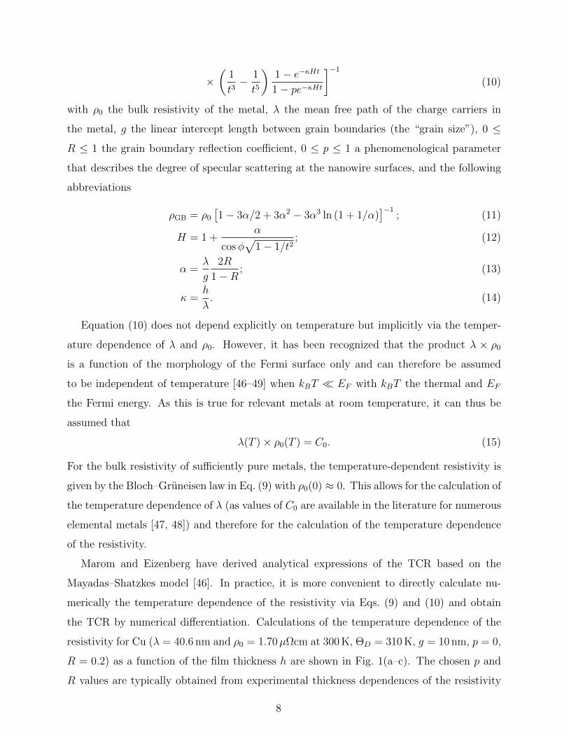
resistivity for Cu (λ = 40.6 nm and ρ0 = 1.70µΩcm at 300 K, ΘD = 310 K, g = 10 nm, p = 0,
R = 0.2) as a function of the film thickness h are shown in Fig. 1(a–c). The chosen p and
R values are typically obtained from experimental thickness dependences of the resistivity
8
0.0 0.2 0.4 0.6 0.8 1.0
7
8
0 100 200 300 400 5000
1
2
3
0 100 200 300 400 5000
10
20
0 10 20 30 40 506
7
8
9
0 100 200 300 400 5000
1
2
3
4
0 100 200 300 400 5000
10
20
0 100 200 300 400 5000
10
20
Temperature (K)
Res
isti
vity
(µΩ
cm)
Temperature (K)
Res
isti
vity
(µΩ
cm)h = 2 nm
(a)
(b)
(d)
(e)
(c)
(f)
Film thickness (nm)
TCR
(1
0-3
µΩ
cm/K
)
Res
isti
vity
(µΩ
cm)
Res
isti
vity
(µΩ
cm)
Temperature (K) Temperature (K) p
TCR
(1
0-3
µΩ
cm/K
)
p = 1.0
p = 0.8
p = 0.6
p = 0.4
p = 0.2
p = 0.0p = 0.0p = 0.2
p = 1.0
Cu bulk TCR
Cu bulk TCR
h = 3 nm
h = 5 nm
h = 10 nmh = 20 nmh = 50 nm
h = 2 nm
h = 3 nm
h = 5 nm
h = 50 nmh = 10 nm
p = 0.6
FIG. 1: (a) Calculated temperature dependence of the resistivity of Cu thin films as a function
of the film thickness using Eq. (10) with λ = 40.6 nm and ρ0 = 1.70µΩcm at 300 K, ΘD = 310 K,
g = 10 nm, p = 0, R = 0.2. (b) Temperature-dependent part of the Cu thin film resistivity,
ρ(T )−ρ(0). (c) TCR at 300 K calculated from the data in (a) and (b). (d) Calculated temperature
dependence of the resistivity of a 3 nm thick Cu film as a function of the surface scattering parameter
p using Eq. (10). The same materials parameters as in (a) were used. (f) Temperature-dependent
part of the 3 nm Cu thin film resistivity in (d), ρ(T )− ρ(0) and (f) TCR at 300 K as a function of
p. For comparison, the bulk Ru TCR value is also shown [dashed lines in (c) and (f)] [50].
[4] with the Mayadas–Shatzkes model. The total calculated resistivity in Fig. 1(a) indicates
a strong increase of the resistivity with decreasing thickness, as expected. By contrast, the
temperature dependent part of the resistivity, ρ(T ) − ρ(0), in Fig. 1(b) and the extracted
TCR value at 300 K in 1(c) are bulk-like [50] for thicker films but increase for thicknesses
below 10 nm. To elucidate this behavior further, the Cu thin film resistivity was calculated
for a thickness of h = 3 nm as a function of the surface roughness scattering parameter p.
The total calculated resistivity in Fig. 1(d) increases with decreasing p since this enhances
the contribution of surface roughness scattering. The temperature dependent part of the
resistivity, ρ(T )− ρ(0), in Fig. 1(e) and the extracted TCR value at 300 K in 1(f) also show
a strong dependence on p. For specular p ∼ 1, the TCR is bulk-like and increases rapidly
with decreasing p. Moreover, additional simulations (not shown) indicate that the TCR
decreases again towards the bulk value when the grain boundary scattering is enhanced by
increasing R or decreasing g. This indicates that it is essentially the ratio of surface and
9
0.0 0.2 0.4 0.6 0.8 1.0
30
40
50
p
TCR
(1
0-3
µΩ
cm/K
)Ru bulk TCR
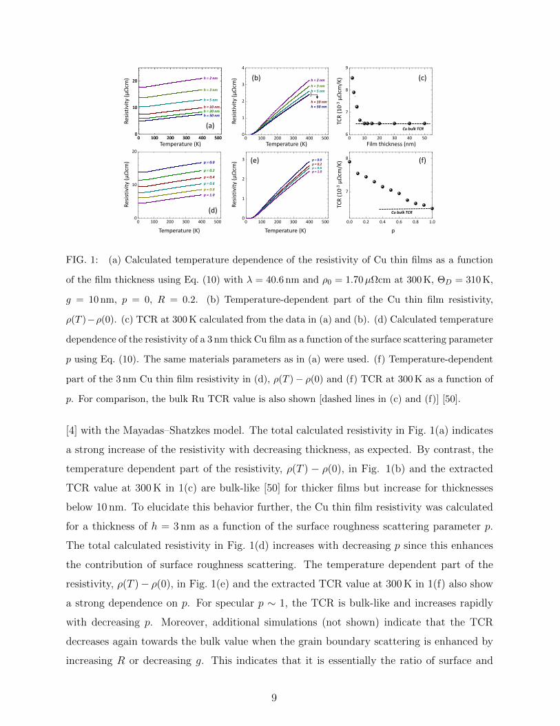
FIG. 2: (a) Calculated room-temperature TCR of a 3 nm thick Ru film for different values of the
surface scattering parameter p following Eq. (10) with λ = 6.6 nm and ρ0 = 7.6µΩcm at 300 K,
ΘD = 420 K, g = 10 nm, R = 0.5. The thin film TCR is equal to the bulk TCR (dashed line) for
all values of p.
grain boundary scattering that determines the TCR, which can be attributed to the “renor-
malization” of the (effective) mean free path due to grain boundary scattering, as discussed
in detail in Ref. [9].
Figure 2 show the calculated TCR at 300 K for Ru (λ = 6.6 nm and ρ0 = 7.6 ΘD = 420 K,
µΩcm at 300 K, g = h, R = 0.5). As for Cu, the experimentally determined R value for
Ru is used [48]. In contrast to Cu, p has no influence on the TCR for the chosen set of
parameters. This can be linked to the shorter mean free path λ of Ru as well as the higher
R, which increases the relative importance of grain boundary scattering and renders surface
roughness scattering negligible. These results are consistent with the experiments and the
discussion in Ref. [48], which has also reported that surface scattering in Ru thin films is
negligible even for p = 0. The results are also consistent with initial experiments on Ru thin
films indicating bulk TCR values for Ru films as thin as 3 nm (not shown). This will be the
topic of a forthcoming publication [51].
The data indicate that the TCR within such semiclassical models is influenced mainly
by the ratio of surface roughness and grain boundary scattering. When grain boundary
scattering dominates, the TCR is bulk-like. However, when the effect of surface scattering
becomes non-negligible, the TCR starts to deviate from its bulk value. Since the Mayadas–
10

Shatzkes model does not obey Matthiessen’s rule for surface roughness and grain boundary
scattering, the individual contributions cannot be regarded separately and the relative im-
portance of surface scattering needs to be deduced from an evaluation of Eq. (10), e.g. by
comparing resistivities calculated for p = 1 and p = 0. Note that the value of p as such does
not determine the importance of surface roughness scattering. In particular, p = 0 does not
necessarily indicate strong surface roughness scattering. For typical thin films with g ≈ h,
grain boundary scattering is generally dominant for Cu and Ru even with p = 0 [48] and
calculated TCR values are within a few % of the bulk value even for ultrathin films of 3 nm
thickness. However, attempts to increase the grain size, e.g. by thermal annealing (lead-
ing to recrystallization and/or grain growth), may change this picture. It should also be
mentioned that for ultrathin films or ultranarrow wires, the surface roughness may become
comparable to the film thickness or wire width at the limit of film closure or wire continuity,
and the used model might lose its applicability [52]. In general, alternative metals with short
mean free path and high grain boundary reflection coefficient R (which is correlated with
higher cohesive energy [53] and thus improved expected electromigration resistance) should
however show less tendency for an increase in TCR than Cu. A more detailed discussion
can be found in Ref. [46].
The above results indicate that the ratio of surface to grain boundary scattering deter-
mines the deviation of the thin film TCR from bulk values. One might assume that a similar
relation also holds qualitatively for nanowires. Due to the larger surface-to-volume ratio,
surface scattering can be expected to have a larger impact for nanowires than for thin films,
as qualitatively argued in Ref. [38]. In absence of a comprehensive quantitative model for
temperature-dependent nanowire resistivities, the TCR measured for thin films might be
used as a proxy for the expected nanowire TCR. When the TCR of thin films is strongly en-
hanced with respect to the bulk value, one can assume that the TCR of nanowires might also
deviate. By contrast, a bulk-like thin film TCR might not necessarily indicate a bulk-like
nanowire TCR. A potential improvement could the usage of measured thin film TCR values
to determine cross-sectional area and resistivity of nanowires of the same material. However,
in absence of a predictive model for nanowire resistivity (and the rather simplistic nature of
the semiclassical thin film models), it is currently not possible to verify the accuracy of this
approach.
Finally, in its derivation, the Mayadas-Shatzkes model assumes the validity of
11

Matthiessen’s rule for grain boundary and phonon scatting (but not for surface roughness
scattering) [9]. As argued above, this is a reasonable assumption for sufficiently pure films.
However, in presence of strong disorder, Matthiessen’s rule has been reported to be violated,
leading to a much weaker temperature dependence of the resistivity and even to zero or neg-
ative TCR values [54, 55]. This suggests that the low thin film TCR values reported in
Ref. [23] might be due to large disorder in the films. Such effects cannot be described within
the Mayadas-Shatzkes model and their quantification is rather difficult, leading to further
potential complications of the determination of TCR values of thin films and nanowires.
The experimental reports mentioned above however suggest that the disorder in current
nanowire (and interconnect) structures is sufficiently low so that disorder effects might be
neglected.
IV. THE TCR METHOD FOR A ROUGH INTERCONNECT LINE
A. Model derivation and discussion
An additional complication that affects the application of the TCR method to scaled
interconnect lines stems from an increased LWR due to lithography and patterning limita-
tions. The derivation of the TCR method in Eqs. (6) and (7) relies on the assumption of
a single uniform cross-sectional area A of the interconnect wire. However, in scaled inter-
connects, this assumption ceases to be obviously justified. This is even more the case for
experimental patterning schemes [36, 37]. In such cases, the 3σ LWR may not be negligible
anymore with respect to the average line width 〈w〉. Therefore, it is of interest to redevelop
the TCR equations by assuming a cross-sectional area that varies along the wire.
A rough interconnect line can be described by a series of small differential resistive ele-
ments of length d` and resistance dR so that the total resistance of the line with length L
is given by R =∫ L0dR. Assuming that each element can be described by Pouillet’s law in
Eq. (1), dR = (ρ[A(`)]/A(`)) d`. Here, A(`) is the cross-sectional area of the element and
ρ[A(`)] its resistivity. Note that the resistivity depends in general on the cross-sectional area
of the element due to finite size effects as discussed above. The resistance of the line can
then be written as
R =
∫ L
0
ρ[A(`)]
A(`)d`. (16)
12
Neglecting thermal expansion effects, the total derivative of the resistance with respect
to the temperature is given by
dR
dT=
∫ L
0
dρ[A(`)]
dT
1
A(`)d`. (17)
Within the approximation of Eq. (4), dρ[A(`)]/dT is independent of the cross-sectional area
and thus
dR
dT=
dρ
dT
∣∣∣∣bulk
∫ L
0
1
A(`)d`
=dρ
dT
∣∣∣∣bulk
L
〈A〉H, (18)
with 〈A〉H = L/(∫ L
01/A(`)d`
)the harmonic mean of the area function A(`).
This shows that the TCR method yields the harmonic mean of the cross-sectional area
for a rough line. The harmonic mean is always smaller than or equal to the arithmetic mean
〈A〉A; in the limit of a uniform area, harmonic and arithmetic means become equal, i.e.
limσ2→0(〈A〉A − 〈A〉H) = 0 with σ2 the variance of the area distribution.
Equation (16) cannot be evaluated for a general ρ[A(`)] and therefore the resistivity
cannot be determined in a straightforward way as in Eq. (7). However, a Taylor expansion
of ρ[A(`)] around 〈A〉H can be used to approximate the area dependence of the resistivity.
Thus,
ρ[A(`)] = ρ (〈A〉H) +dρ
dA
∣∣∣∣〈A〉H
(A(`)− 〈A〉H)
+1
2
d2ρ
dA2
∣∣∣∣〈A〉H
(A(`)− 〈A〉H)2 + . . .
≡ 〈ρ〉+ ξ (A(`)− 〈A〉H)
+1
2η (A(`)− 〈A〉H)2 + . . . (19)
with 〈ρ〉 the resistivity at the harmonic mean of A(`). ξ and η denote the first and second
derivatives of ρ(A) at 〈A〉H , respectively. In a first-order approximation, the resistance in
Eq. (16) then becomes
R =
∫ L
0
ρ(`)
A(`)d` ≈
∫ L
0
〈ρ〉+ ξ (A(`)− 〈A〉H)
A(`)d`
=〈ρ〉L〈A〉H
+ Lξ − ξ 〈A〉H∫ L
0
1
A(`)d`
=〈ρ〉L〈A〉H
(20)
13

Solving the system of Eqs. (18) and (20) leads then to the first-order TCR equations for
rough lines, analogously to Eqs. (6) and (7):
〈A〉H = Ldρ
dT
∣∣∣∣bulk
(dR
dT
)−1; (21)
ρ (〈A〉H) = Rdρ
dT
∣∣∣∣bulk
(dR
dT
)−1. (22)
The TCR method yields thus the harmonic mean of the cross-sectional area 〈A〉H and to
first order the resistivity at 〈A〉H . Therefore, the resistivity vs. area curve extracted by the
TCR method from a set of rough wires with different 〈A〉H represent quantitatively (to first
order) the area dependence of the resistivity ρ(A).
The accuracy of the first-order Taylor expansion can be tested by calculating the second-
order correction to Eq. (20), leading to
∆R =η
2
∫ L
0
(A(`)− 〈A〉H)2
A(`)d`
=η
2(L 〈A〉A − 2L 〈A〉H + L 〈A〉H)
=Lη
2(〈A〉A − 〈A〉H) . (23)
Thus, the correction is proportional to the second derivative of ρ(A) as well as the difference
between arithmetic and harmonic means of A(`). Note that for uniform lines, 〈A〉A =
〈A〉H ≡ A as well as ∆R = 0 and Eqs. (21) and (22) turn into Eqs. (6) and (7).
The second-order correction ∆R cannot be evaluated for a general A(`). However, since
〈A〉A ≥ 〈A〉H ≥ 0, an upper limit is given by
∆R ≤ Lη
2〈A〉A (24)
Practically, the upper limit of the second-order correction could e.g. be estimated by the
apparent physical cross-sectional area (e.g. measured by TEM) as an estimator of 〈A〉Aand the second derivative of the obtained ρ(A) curve. For small Cu and Ru wires, ηCu ∼
10−4 µΩcm/nm4 and ηRu ∼ 10−5 µΩcm/nm4, respectively. For a very rough wire with an
arithmetic average area of 100 nm2 (and a harmonic average area of ∼ 0 nm2), the correction
is thus below 10 Ω/µm for Ru and 100 Ω/µm for Cu. Typical line resistances for 100 nm2
cross-sectional area are above 1 kΩ/µm and thus the corrections are small to negligible even
in such an extreme case. The corrections are not expected to depend strongly on the cross-
sectional area as η decreases rapidly with increasing cross-sectional area or line width. As
14
shown in the next section, 〈A〉A− 〈A〉H 〈A〉A for realistic LWRs and thus the real values
of ∆R will be much smaller. Therefore, second-order corrections can typically be neglected.
B. Case study: truncated Gaussian LWR statistics
The variability of the dimensions of an interconnect wire is typically described by the
rms LWR as well as a lateral correlation length (or the roughness power spectrum). As the
correlation length is not expected to affect much the resistivity of the conductor as long as
Pouillet’s law remains applicable, it is mainly of interest to understand the dependence of
the electrical cross-sectional area determined by TCR, 〈A〉H , on the LWR.
Let us consider a rectangular interconnect line with width w, height h, and area A = w×h.
The width w is treated as a stochastic variable characterized by a probability function that
can be described by an arithmetic mean 〈w〉 and a variance σ2w. For simplicity, it is assumed
that the line height h does not vary along the line and thus 〈A〉A = 〈w〉×h and σ2A = σ2
w×h2.
The line height variation with an average height of 〈h〉 and a variance σ2h can however be
easily included in the model using 〈A〉A = 〈w〉 × 〈h〉 and σ2A = σ2
w × 〈h〉2 + σ2
h × 〈w〉2.
Experimentally, the line width has been found to follow a Gaussian distribution [56]. The
probability function for the cross-sectional area is then
P (A) =1√
2πσ2A
exp
(−(A− 〈A〉A)2
2σ2A
)(25)
and the harmonic average of the area can then be calculated by
〈A〉H =
(∫ ∞−∞
P (A)
AdA
)−1. (26)
From a mathematical viewpoint, the usage of Gaussian statistics is somewhat problematic
since a Gaussian has a finite probability at A = 0 and therefore the harmonic average of the
area is always zero. In practice however, for interconnects with high yield, Gaussian statistics
can be assumed to be obeyed only in a certain window around the mean line width with
a rapid falloff to zero probability outside. This means that Eq. (26) can be approximately
written as
〈A〉H =
(∫ 〈A〉A+c
〈A〉A−c
P (A)
AdA
)−1, (27)
with a suitably chosen cutoff c. If 〈A〉A σA, the divergence of P (A)/A at A = 0 is slow
and 〈A〉H does not depend critically on the choice of c.
15
0 2 4 6 8 10160
170
180
190
200
LWR (3σ, nm)
Elec
tric
al a
rea,
<A
>H
(nm
2)
= 10 nmh = 20 nmw
A A
FIG. 3: Harmonic area average, 〈A〉H , assuming a truncated Gaussian distribution for the inter-
connect line width as a function of the 3σ LWR. The mean line width 〈w〉 was 10 nm and the line
height h was fixed at 20 nm, as discussed in the text, i.e. the mean cross-sectional area (arithmetic
mean) was 200 nm2 (dashed line).
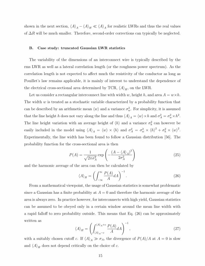
Figure 3 shows the calculated value of 〈A〉H for a line with an average width of 〈w〉 =
10 nm and a fixed height of h = 20 nm as a function of the 3σ LWR under the above
assumptions. Here, the cutoff was chosen as 〈A〉A− c = 0.1 nm2. As expected, the choice of
the cutoff close to zero had negligible influence on 〈A〉H .
One can see that an increasing 3σ LWR leads to a reduction of 〈A〉H with respect to
〈A〉A = 200 nm2. However, rather large values of 3σ ≈ 8 nm are required for a 10% reduction
of 〈A〉H with respect to 〈A〉A. In real interconnects, variations of the line height will lead to
larger area variances and to larger deviations, as discussed above. Nonetheless, the above
case study shows that the TCR method can be expected to lead to accurate mean line areas
if the 3σ LWR is much smaller than the average line width, which is typically the case for
interconnects with high yield.
V. THE TCR METHOD FOR AN INTERCONNECT LINE WITH A CONDUC-
TIVE LINER
In scaled interconnects, the volume available for the center conductor (commonly Cu)
is increasingly reduced because barrier and liner layers are difficult to scale. In former
technology nodes, TaN/Ta was used as the barrier/liner combination occupying typically
16

a volume fraction of less than 10%. With a Cu resistivity close to the bulk value and
much larger Ta and TaN resistivities, the contribution of the liner and barrier to the line
conductivity was negligible. In this case, barrier and liner could be treated as insulators
from an electrical point of view and the TCR method could be used to extract area and
resistivity of the center conductor.
However, in future (Cu-based) technology nodes, the volume fraction occupied by barrier
and liner(s) may reach several 10% at line widths of the order of 10 nm. In addition,
lower resistivity liners, such as Co and Ru have been introduced. Therefore, the parallel
conductance due to barriers and liners may not be negligible and may affect the TCR analysis
of the interconnect wire. It is evident that the extraction of four unknown parameters, i.e.
the resistivities of the center conductor, ρcc, and the liner, ρli, as well as their (electrical)
areas, Acc and Ali, is not possible from the two available measurements, R and dR/dT .
Therefore, an accurate TCR analysis of interconnects with a significant contribution of the
barrier/liner combination to the conductance is not possible without further knowledge,
e.g. of the resistivity and the area of the liner. However, the conditions, under which the
assumption of an “insulating” barrier/liner is valid and the TCR method yields accurate
values for the resistivity and area of the center conductor can be discussed. Within such
an approach, when approximate values for resistance, resistivity, and area ratios of center
conductor and barrier/liner are available, approximate correction factors can be calculated
and errors due to the presence of barrier and liner can be estimated.
The resistance of an interconnect line consisting of two parallel conductors, i.e. the center
conductor with resistance Rcc and a barrier/liner with resistance Rli is given by
R =
(1
Rcc
+1
Rli
)−1=
RccRli
Rcc +Rli
. (28)
The total derivative of the resistance with respect to the temperature is then
dR
dT=
∂R
∂Rcc
dRcc
dT+
∂R
∂Rli
dRli
dT
=R2
li
(Rcc +Rli)2
dRcc
dT+
R2cc
(Rcc +Rli)2
dRli
dT
=R2
R2cc
dRcc
dT+R2
R2li
dRli
dT. (29)
17
In principle, when all necessary information about the liner properties (Ali, ρli, dρli/dT )
is available, Eqs. (28) and (29) can be solved to deduce Acc and ρcc in the same TCR
approximation as above. However, this will be rarely the case in practice and therefore
explicit formulae for Acc and ρcc are only of limited interest. By contrast, for current
interconnects, the contribution of the liner to the total line conductance will still be rather
small. In such cases, one can then ask the question, under which conditions the liner
contribution is sufficiently small to lead to acceptable errors in the extraction of Acc and ρcc
when the parallel conductance of barrier/liner is neglected. To this aim, Rli can be treated
as a “perturbation”, leading to appropriate correction factors for the TCR Eqs. (6) and (7).
Although the correction factors may not be accurately quantifiable in practice, approximate
values can be determined when the liner resistance can be estimated and the accuracy of
the TCR method can be semi-quantitatively assessed.
For a weak liner contribution, it can be assumed that Rcc Rli and all quadratic terms
in Rcc/Rli can be neglected. Thus, the total differential in Eq. (29) becomes
dR
dT=
R2li
(Rcc +Rli)2
dRcc
dT+
R2cc
(Rcc +Rli)2
dRli
dT(30)
≈ Rcc1
(1 +Rcc/Rli)2
1
ρcc
dρccdT
+R2
cc
Rli
1
(1 +Rcc/Rli)2
1
ρli
dρlidT
. (31)
A further quantitative analysis of the above equations to obtain electrical areas of the center
conductor and/or the liner requires the knowledge of the TCR of the liner, dRli/dT or
alternatively dρli/dT . Some quantitative insight in the effect of the liner can be gained
from two different approximations. For many pure bulk metals, values of (1/ρ)(dρ/dT )
are of the same order of magnitude. For example, (1/ρ)(dρ/dT ) at 0 C is 0.0043 K−1 for
Cu, 0.0056 K−1 for Co, or 0.0045 K−1 for Ru [50]. Therefore, one can assume that the
relative temperature derivatives of the resistivities of center conductor and liner are equal,
i.e. (1/ρcc)(dρcc/dT ) = (1/ρli)(dρli/dT ). In addition, for “highly defective” (or impure)
layers, one can often assume dρ/dT ∼ 0 [23] since Matthiessen’s rule is violated in this case.
This amounts to neglecting the second term ∝ dρli/dT in Eq. (31).
Assuming dρli/dT = 0, Eq. (30) can be combined with Pouillet’s law in Eq. (1) to obtain
the electrical area of the center conductor, leading to
18

Acc = αLdρccdT
∣∣∣∣bulk
(dR
dT
)−1, (32)
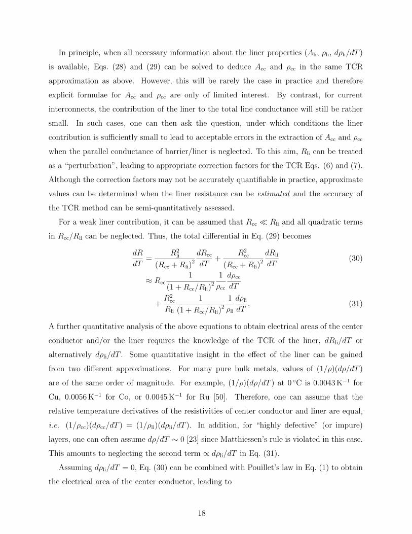
with the correction factor due to the contribution due to the liner
α =1
(1 +Rcc/Rli)2 . (33)
For small Rcc/Rli . 0.1, the relation can be approximated as α ≈ 1− 2Rcc/Rli.
Alternatively, one can assume that the relative temperature derivatives of the resistivities
of center conductor and liner are equal, i.e. (1/ρcc)(dρcc/dT ) = (1/ρli)(dρli/dT ). This leads
to the same equation of the electrical area of the center conductor as in Eq. (32), albeit with
a correction factor of
α =1 + R2
cc
R2li
Acc
Ali
(1 +Rcc/Rli)2 . (34)
Here, Acc and Ali are the cross-sectional areas of the center conductor and the liner, respec-
tively.
In all relevant cases, when the liner resistivity is smaller than that of the center conductor,
α ≤ 1. Therefore, ignoring the contribution of the liner to the total line resistance, i.e.
assuming α = 1, leads to an overestimation of the area of the center conductor. Of course,
the correction factor α cannot be calculated in the general case as Rcc and Rli are a priori
unknown. However, Eq. (32) can be used to estimate the error of the electrical area when a
reasonable estimate of the liner and center conductor resistances can be obtained (consistent
with the total measured resistance). An example plot of the correction factor α as a function
of Rcc/Rli is shown in Fig. 4. The figure shows the correction factors derived from Eqs. (33)
and (34) for Acc/Ali = 1.5. It is clear from Eqs. (33) and (34) that absolute values of Rcc and
Rli do not affect α, which depends only on the ratio. The graph shows that corrections start
to become considerable (of the order of 20%) when the liner contribution approaches 10%
of the total conductance of the line, rather independent of the approximation of Eqs. (30)
and (31).
In the second step, the resistivity of the center conductor will be assessed in presence of
the barrier/liner. Eq. (28) can be approximated to first order as
R =RccRli
Rcc +Rli
≈ Rcc
(1− Rcc
Rli
). (35)
19
0.01 0.1 10.0
0.2
0.4
0.6
0.8
1.0
Rcc/Rli
Are
a co
rrec
tio
n f
acto
r α
dρli/dT = 0
(1/ρcc)(dρcc/dT)
= (1/ρli)(dρli/dT)
FIG. 4: Electric area correction factor α assuming dρli/dT = 0 (black dots) and assuming equal
relative TCR values of center conductor and liner, i.e. (1/ρcc)(dρcc/dT ) = (1/ρli)(dρli/dT ) (blue
dots).
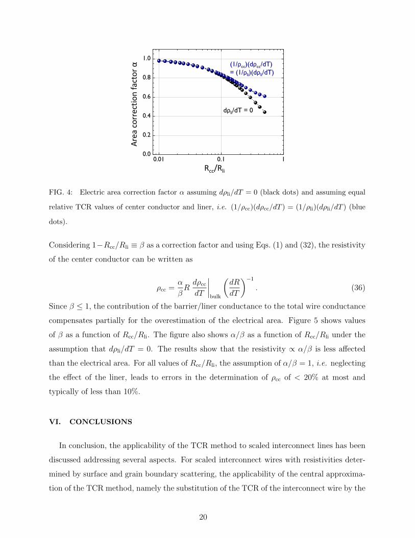
Considering 1−Rcc/Rli ≡ β as a correction factor and using Eqs. (1) and (32), the resistivity
of the center conductor can be written as
ρcc =α
βRdρccdT
∣∣∣∣bulk
(dR
dT
)−1. (36)
Since β ≤ 1, the contribution of the barrier/liner conductance to the total wire conductance
compensates partially for the overestimation of the electrical area. Figure 5 shows values
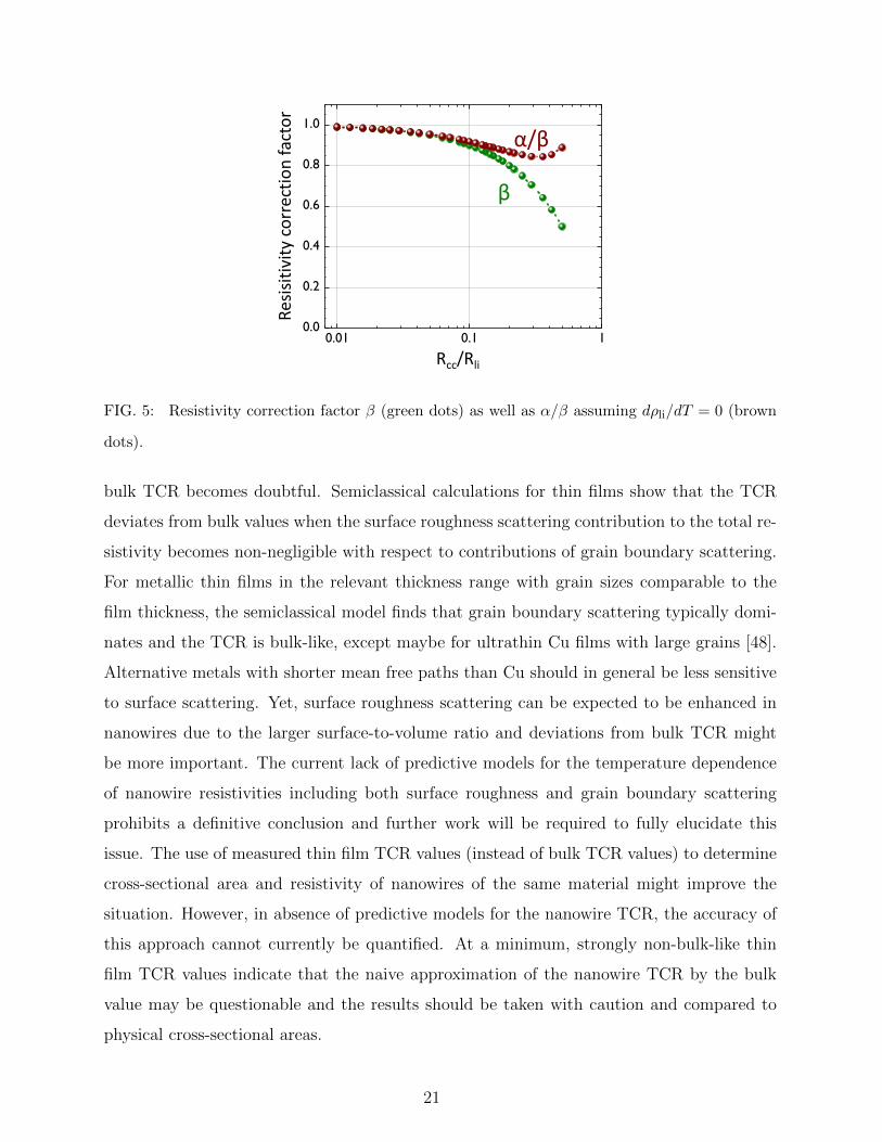
of β as a function of Rcc/Rli. The figure also shows α/β as a function of Rcc/Rli under the
assumption that dρli/dT = 0. The results show that the resistivity ∝ α/β is less affected
than the electrical area. For all values of Rcc/Rli, the assumption of α/β = 1, i.e. neglecting
the effect of the liner, leads to errors in the determination of ρcc of < 20% at most and
typically of less than 10%.
VI. CONCLUSIONS
In conclusion, the applicability of the TCR method to scaled interconnect lines has been
discussed addressing several aspects. For scaled interconnect wires with resistivities deter-
mined by surface and grain boundary scattering, the applicability of the central approxima-
tion of the TCR method, namely the substitution of the TCR of the interconnect wire by the
20
0.01 0.1 10.0
0.2
0.4
0.6
0.8
1.0
Rcc/Rli
Res
isit
ivit
yco
rrec
tio
n f
acto
r
β
α/β
FIG. 5: Resistivity correction factor β (green dots) as well as α/β assuming dρli/dT = 0 (brown
dots).
bulk TCR becomes doubtful. Semiclassical calculations for thin films show that the TCR
deviates from bulk values when the surface roughness scattering contribution to the total re-
sistivity becomes non-negligible with respect to contributions of grain boundary scattering.
For metallic thin films in the relevant thickness range with grain sizes comparable to the
film thickness, the semiclassical model finds that grain boundary scattering typically domi-
nates and the TCR is bulk-like, except maybe for ultrathin Cu films with large grains [48].
Alternative metals with shorter mean free paths than Cu should in general be less sensitive
to surface scattering. Yet, surface roughness scattering can be expected to be enhanced in
nanowires due to the larger surface-to-volume ratio and deviations from bulk TCR might
be more important. The current lack of predictive models for the temperature dependence
of nanowire resistivities including both surface roughness and grain boundary scattering
prohibits a definitive conclusion and further work will be required to fully elucidate this
issue. The use of measured thin film TCR values (instead of bulk TCR values) to determine
cross-sectional area and resistivity of nanowires of the same material might improve the
situation. However, in absence of predictive models for the nanowire TCR, the accuracy of
this approach cannot currently be quantified. At a minimum, strongly non-bulk-like thin
film TCR values indicate that the naive approximation of the nanowire TCR by the bulk
value may be questionable and the results should be taken with caution and compared to
physical cross-sectional areas.
21
In addition, to assess whether it can also be applied to rough interconnect lines, the
TCR method has been rederived with an area that is allowed to vary along the line and
an area-dependent resistivity that therefore also varies along the line. In such a case, it is
shown that the TCR method yields the harmonic average of the area distribution function
as well as, to first order, the correct value for the resistivity at the extracted area. A case
study for Gaussian roughness indicates that the harmonic average is within a few % of the
arithmetic average for 3σ LWR values that are comparable to what is achieved by current
patterning techniques. Thus, the results of the TCR method are not expected to be affected
for scaled interconnect lines with good yield.
Finally, the effect of a conductive barrier/liner layer on the TCR method has been dis-
cussed. The cross-sectional areas and resistivities of barrier/liner and center conductor can-
not be determined independently by the TCR method. While the effect of the barrier/liner
parallel conductance can be corrected for if it is accurately known, this will be the case only
in rare situations. In current technology nodes, the contribution of the barrier and liners
to the total conductance is still rather small and it can thus be treated as “perturbation”
of the conductance of the center conductor. For such a case, the conditions, under which
the assumption of a negligible barrier/liner contribution (“insulating” barrier/liner) is valid,
have been derived. Within this model, approximate correction factors can be calculated
when approximate values for resistance, resistivity, and area ratios of center conductor and
barrier/liner are known. The results show that neglecting barrier/liner resistance leads to
an overestimation of the center conductor area that is approximately twice the relative con-
ductivity contribution. An accuracy in cross-sectional area of 10% thus requires that the
barrier/liner contributes less than 5% to the total interconnect conductance. By contrast,
the resistivity is less affected and remains typically within 10% of the center conductor value
even for relatively large relative barrier/liner conductance.
Acknowledgement
The author would like to thank Shibesh Dutta (imec), Florin Ciubotaru (imec), Kristof
Moors (University of Luxembourg) and Christian Witt (GlobalFoundries) for many valu-
able discussions. This work has been supported by imec’s industrial affiliate program on
22

nanointerconnects.
[1] Meindl, J.D., Beyond Moore’s Law: the interconnect era. Comp. Sci. Engineer. 5, 20–24
(2003). DOI: 10.1109/MCISE.2003.1166548
[2] Clarke, J.S., George, C., Jezewski, C., Maestre Caro, A., Michalak, D., Torres, J. Process
technology scaling in an increasingly interconnect dominated world. 2014 IEEE Symp. VLSI
Technol. Techn. Dig., pp. 1–2 (2014). DOI: 10.1109/VLSIT.2014.6894407
[3] Baklanov, M.R., Adelmann, C., Zhao, L., de Gendt, S. Advanced interconnects: materi-
als, processing, and reliability. ECS J. Solid State Sci. Technol. 4, Y1–Y4 (2015). DOI:
10.1149/2.0271501jss
[4] Josell, D., Brongersma, S.H., Tokei, Z. Size-dependent resistivity in nanoscale interconnects.
Ann. Rev. Mater. Res. 39, 231–254 (2009). DOI: 10.1146/annurev-matsci-082908-145415
[5] Fuchs, K., The conductivity of thin metallic films according to the electron the-
ory of metals. Mathem. Proc. Cambridge Philos. Soc. 34, 100–108 (1938). DOI:
10.1017/S0305004100019952
[6] Sondheimer, E.H. The mean free path of electrons in metals. Adv. Phys. 1, 1–42 (1952). DOI:
10.1080/00018730110102187
[7] Soffer, S.B. Statistical model for the size effect in electrical conduction. J. Appl. Phys. 38,
1710–1715 (1967). DOI: 10.1063/1.1709746
[8] Mayadas, A.F., Shatzkes, M., Janak, J.F. Electrical resistivity model for polycrystalline films:
the case of specular reflection at external surfaces. Appl. Phys. Lett. 14, 345–347 (1969). DOI:
10.1063/1.1652680
[9] Mayadas, A.F., Shatzkes, M. Electrical-resistivity model for polycrystalline films: the case
of arbitrary reflection at external surfaces. Phys. Rev. B 1, 1382–1389 (1970). DOI:
10.1103/PhysRevB.1.1382
[10] Iwai, H., CMOS downsizing toward sub-10 nm. Solid-State Electronics 48, 497–503 (2004).
DOI: 10.1016/j.sse.2003.09.034
[11] Tokei, Z., Ciofi, I., Roussel, P., Debacker, P., Raghavan, P., van der Veen, M.H., Jourdan,
N., Wilson, C.J., Gonzalez, V.V., Adelmann, C., Wen, L., Croes, K., Varela Pedreira, O.,
Moors, K., Krishtab, M., Armini, S., Bommels, J. On-chip interconnect trends, challenges
23

and solutions: how to keep RC and reliability under control. 2016 IEEE Symp. VLSI Technol.
Techn. Dig., pp. 1–2 (2016). DOI: 10.1109/VLSIT.2016.7573426
[12] Kapur, P., McVittie, J.P., Saraswat, K.C. Technology and reliability constrained future copper
interconnects. I. Resistance modeling. IEEE Trans. Electron Devices 49, 590–597 (2002). DOI:
10.1109/16.992867
[13] Adelmann, C., Wen, L.G., Peter, A.P., Siew, Y.K., Croes, K., Swerts, J., Popovici, M.,
Sankaran, K., Pourtois, G., Elshocht, S.V., Bommels, J., Tokei, Z. Alternative metals for
advanced interconnects. Proc. 2014 IEEE Intern. Interconnect Technol. Conf. (IITC), pp.
173–176 (2014). DOI: 10.1109/IITC.2014.6831863
[14] Pan, C., Naeemi, A. A proposal for a novel hybrid interconnect technology for the end of the
roadmap. IEEE Electron Device Lett. 35, 250–252 (2014). DOI: 10.1109/LED.2013.2291783
[15] Schafft, H.A., Mayo, S., Jones, S.N., Suehle, J.S. An electrical method for determining the
thickness of metal films and the cross-sectional area of metal lines. Proc. 1994 IEEE Intern.
Integr. Reliab. Workshop (IRWS), 5–11 (1994). DOI: 10.1109/IRWS.1994.515820
[16] Li, H., Jin, S., Proost, J., Van Hove, M., Froyen, L., Maex, K. A new approach for the mea-
surement of resistivity and cross-sectional area of an aluminium interconnect line: principle
and applications. In Cheung, R., Klein, J., Tsubouchi, K., Murakami, M., Kobayashi, N., eds.
Advanced Metallization and Interconnect Systems for ULSI Applications in 1997, pp. 197–203
(Materials Research Society, Warrendale, PA, 1998). ISBN: 978-1558994126
[17] Schuster, C.E., Vangel, M.G., Schafft, H.A. Improved estimation of the resistivity of pure
copper and electrical determination of thin copper film dimensions. Microelectron. Reliab. 41,
239 (2001). DOI: 10.1016/S0026-2714(00)00227-4
[18] Bid, A., Bora, A., Raychaudhuri, A.K. Temperature dependence of the resistance of metallic
nanowires of diameter >15 nm: applicability of Bloch-Gruneisen theorem. Phys. Rev. B 74,
035426 (2006). DOI: 10.1103/PhysRevB.74.035426
[19] Ou, M.N., Yang, T.J., Harutyunyan, S.R., Chen, Y.Y., Chen, C.D., Lai, S.J. Electrical
and thermal transport in single nickel nanowire. Appl. Phys. Lett. 92, 063101 (2008). DOI:
10.1063/1.2839572
[20] Yoneoka, S., Lee, J., Liger, M., Yama, G., Kodama, T., Gunji, M., Provine, J., Howe,
R.T., Goodson, K.E., Kenny, T.W. Electrical and thermal conduction in atomic layer
deposition nanobridges down to 7 nm thickness. Nano Lett. 12, 683–686 (2012). DOI:
24
10.1021/nl203548w
[21] Kolesnik-Gray, M.M., Hansel, S., Boese, M., Krstic, V. Impact of surface and twin-boundary
scattering on the electrical transport properties of Ag nanowires. Solid State Commun. 202,
48–51 (2015). DOI: 10.1016/j.ssc.2014.11.006
[22] Cheng, Z., Liu, L., Xu, S., Lu, M., Wang, X. Temperature dependence of electrical and thermal
conduction in single silver nanowire. Sci. Rep. 5, 10718 (2015). DOI: 10.1038/srep10718
[23] Belser R.B., Hicklin, W.H. Temperature coefficients of resistance of metallic films in the tem-
perature range 25 to 600 C. J. Appl. Phys. 30, 313–322 (1959). DOI: 10.1063/1.1735158
[24] van Attekum, P.M.T.M., Woerlee, P.H., Verkade, G.C., Hoeben, A.A.M. Influence of grain
boundaries and surface Debye temperature on the electrical resistance of thin gold films. Phys.
Rev. B 29, 645–650 (1984). DOI: 10.1103/PhysRevB.29.645
[25] De Vries, J.W.C. Temperature and thickness dependence of the resistivity of thin polycrystalline
aluminium, cobalt, nickel, palladium, silver and gold films. Thin Solid Films 167, 25–32 (1988).
DOI: 10.1016/0040-6090(88)90478-6
[26] Kim, S., Suhl, H., Schuller, I.K. Surface phonon scattering in the electrical resistivity on Co/Ni
superlattices. Phys. Rev. Lett. 78, 322–325 (1997). DOI: 10.1103/PhysRevLett.78.322
[27] Steinlesberger, G., Engelhardt, M., Schindler, G., Steinhogl, von Glasow, W.A.,
Mosig, K., Bertagnolli, E. Electrical assessment of copper damascene interconnects
down to sub-50 nm feature sizes. Microelectron. Eng. 64, 409–416 (2002). DOI:
10.1016/S0167-9317(02)00815-8
[28] Kastle, G., Boyen, H.-G., Schroder, A., Plettl, A., Ziemann, P. Size effect of the resistivity of
thin epitaxial gold films. Phys. Rev. B 70, 165414 (2004). DOI: 10.1103/PhysRevB.70.165414
[29] Ma, W., Zhang, X., Takahashi, K. Electrical properties and reduced Debye tempera-
ture of polycrystalline thin gold films. J. Phys. D: Appl. Phys. 43, 465301 (2010). DOI:
10.1088/0022-3727/43/46/465301
[30] van Delft, F.C.M.J.M., Koster van Groos, M.J., Graaff, R.A.G.D., Langeveld, A.D.V.,
Nieuwenhuys, B.E. Determination of surface Debye temperatures by LEED. Surf. Sci. 189190,
695–703 (1987). DOI: 10.1016/S0039-6028(87)80502-2
[31] Kiguchi, M., Yokoyama, T., Matsumura, D., Kondoh, H., Endo, O., Ohta, T. Surface struc-
tures and thermal vibrations of Ni and Cu thin films studied by extended x-ray-absorption fine
structure. Phys. Rev. B 61, 14020–14027 (2000). DOI: 10.1103/PhysRevB.61.14020
25

[32] Carles, R., Benzo, P., Pecassou, B., Bonafos, C. Vibrational density of states and thermo-
dynamics at the nanoscale: the 3D–2D transition in gold nanostructures. Sci. Rep. 6, 39164
(2016). DOI’: 10.1038/srep39164
[33] Volklein, F., Reith, H., Cornelius, T.W., Rauber, M., Neumann, R. The experimental inves-
tigation of thermal conductivity and the Wiedemann–Franz law for single metallic nanowires.
Nanotechnology 20 325706 (2009). DOI: 10.1088/0957-4484/20/32/325706
[34] Verstraete, M.J., Gonze, X. Phonon band structure and electron-phonon interactions in metal-
lic nanowires. Phys. Rev. B 74, 153408 (2006). DOI: 10.1103/PhysRevB.74.153408
[35] Simbeck, A.J., Lanzillo, N., Kharche, N., Verstraete, M.J., Nayak, S.K. Aluminum conducts
better than copper at the atomic scale: a first-principles study of metallic atomic wires. ACS
Nano 6, 10449–10455 (2012). DOI: 10.1021/nn303950b
[36] Dutta, S., Kundu, S., Gupta, A., Jamieson, G., Gomez Granados, J.F., Bommels, J., Wilson,
C.J., Tokei, Z., Adelmann, C. Highly scaled ruthenium interconnects. IEEE Electron Device
Lett. 38, 949–951 (2017). DOI: 10.1109/LED.2017.2709248
[37] Dutta, S., Kundu, S., Wen, L., Jamieson, G., Croes, K., Gupta, A., Bommels, J., Wilson,
C.J., Adelmann, C., Tokei, Z. Ruthenium interconnects with 58 nm2 cross-section area using
a metal-spacer process. Proc. 2017 IEEE Intern. Interconnect Technol. Conf. (IITC), pp. 1–3
(2017). DOI: 10.1109/IITC-AMC.2017.7968937
[38] Dutta, S., Moors, K., Vandemaele, M., Adelmann, C. Finite size effects in highly
scaled ruthenium interconnects. IEEE Electron Device Lett. 39, 268–271 (2018). DOI:
10.1109/LED.2017.2788889
[39] Zhou, Y., Sreekala, S., Ajayan, P.M., Nayak, S.K. Resistance of copper nanowires and compar-
ison with carbon nanotube bundles for interconnect applications using first principles calcula-
tions. J. Phys.: Condens. Matter 20, 095209 (2008). DOI: 10.1088/0953-8984/20/9/095209
[40] Jones, S.L.T., Sanchez–Soares, A., Plombon, J.J., Kaushik, A.P., Nagle, R.E., Clarke, J.S.,
Greer, J.C. Electron transport properties of sub-3-nm diameter copper nanowires. Phys. Rev.
B 92, 115413 (2015). DOI: 10.1103/PhysRevB.92.115413
[41] Hegde, G., Bowen, R.C., Rodder, M.S. Lower limits of line resistance in nanocrystalline back
end of line Cu interconnects. Appl. Phys. Lett. 109, 193106 (2016). DOI: 10.1063/1.4967196
[42] Lanzillo, N.A. Ab initio evaluation of electron transport properties of Pt, Rh, Ir, and Pd
nanowires for advanced interconnect applications. J. Appl. Phys. 121, 175104 (2017). DOI:
26
10.1063/1.4983072
[43] Tesanovic, Z., Jaric, M.V., Maekawa, S. Quantum transport and surface scattering. Phys. Rev.
Lett. 57, 2760–2763 (1986). DOI: 10.1103/PhysRevLett.57.2760
[44] Sheng, L., Xing, D.Y., Wang, Z.D. Transport theory in metallic films: crossover
from the classical to the quantum regime. Phys. Rev. B 51, 7325–7328 (1995). DOI:
10.1103/PhysRevB.51.7325
[45] Zhou, T., Gall, D. Resistivity scaling due to electron surface scattering in thin metal layers.
Phys. Rev. B 97, 165406 (2018). DOI: 10.1103/PhysRevB.97.165406
[46] Marom H., Eizenberg, M. The temperature dependence of resistivity in thin metal films. J.
Appl. Phys. 96, 3319–3323 (2004). DOI: 10.1063/1.1784552
[47] Gall, D. Electron mean free path in elemental metals. J. Appl. Phys. 119, 085101 (2016). DOI:
10.1063/1.4942216
[48] Dutta, S., Sankaran, K., Moors, K., Pourtois, G., Van Elshocht, S., Bommels, J., Vandervorst,
W., Tokei, Z., Adelmann, C. Thickness dependence of the resistivity of platinum-group metal
thin films. J. Appl. Phys. 122, 025107 (2017). DOI: 10.1063/1.4992089
[49] Zheng, P., Gall, D. The anisotropic size effect of the electrical resistivity of metal thin films:
tungsten. J. Appl. Phys. 122, 135301 (2017). DOI: 10.1063/1.5004118
[50] Bass, J. Pure metal resistivities at T = 273 .2 K. In Hellwege, K.H., Olsen, J.L., eds. Electri-
cal resistivity, Kondo and spin fluctuation systems, spin glasses and thermopower. Landolt-
Bornstein – Group III Condensed Matter, Vol. 15a, Sec. 1.2.1 (Springer, Berlin, Heidelberg).
DOI: 10.1007/10307022 3
[51] Siniscalchi, M., Mertens, S., Witters, T., Meersschaut, J., Adelmann C. Temperature coeffi-
cents of the resistivity of alternative metal thin films, unpublished.
[52] Zhou, T., Zheng, P., Pandey, S.C., Sundararaman, R., Gall, D. The electrical resistivity of
rough thin films: a model based on electron reflection at discrete step edges. J. Appl. Phys.
123, 155107 (2018. DOI: 10.1063/1.5020577
[53] Zhu, Y.F., Lang, X.Y., Zheng, W.T., Jiang, Q. Electron scattering and electrical conductance
in polycrystalline metallic films and wires: impact of grain boundary scattering related to
melting point. ACS Nano 4, 3781–3788 (2010). DOI: 10.1021/nn101014k
[54] Mooij, J.H. Electrical conduction in concentrated disordered transition metal alloys. phys. stat.
sol. (a) 17, 521–530 (1973). DOI: 10.1002/pssa.2210170217
27
[55] Tsuei, C.C. Nonuniversality of the Mooij correlation—the temperature coefficient of elec-
trical resistivity of disordered metals. Phys. Rev. Lett. 57, 1943–1946 (1986). DOI:
10.1103/PhysRevLett.57.1943
[56] Leunissen, L.H.A., Lorusso, G.F., Ercken, M., Croon, J.A., Yang, H., Azordegan, A., DiBiase,
T. Full spectral analysis of line width roughness. Proc. SPIE 5752, 499–510 (2005). DOI:
10.1117/12.600185
28