choice based credit system - gct.ac.in
TRANSCRIPT

GOVERNMENT COLLEGE OF TECHNOLOGY
COIMBATORE-641 013
DEPARTMENT OF ELECTRONICS AND COMMUNICATION ENGINEERING
CHOICE BASED CREDIT SYSTEM DURING 2016 ONWARDS
BRANCH: M.E. – VLSI DESIGN - FULL TIME
SYLLABUS
VISION OF THE INSTITUTION
To emerge as a centre of excellence and eminence by imparting futuristic technical
education in keeping with global standards, making our students technologically competent
and ethically strong so that they can readily contribute to the rapid advancement of society
and mankind.
MISSION OF THE INSTITUTION
To achieve Academic excellence through innovative teaching and learning practices.
To enhance employability and entrepreneurship.
To improve the research competence to address societal needs.
To inculcate a culture that supports and reinforces ethical, professional behaviours for
a harmonious and prosperous society.
VISION OF THE DEPARTMENT
The vision of ECE department is to become pioneer in higher learning and research and to
produce creative solution to societal needs.
MISSION OF THE DEPARTMENT
1. To provide excellence in education, research and public service.
2. To provide quality education and to make the students entrepreneur and employable.
3. Continuous upgradation of techniques for reaching heights of excellence in a global
perspectives.
PROGRAM OUTCOMES
Ability to
1. Acquire in-depth knowledge in the field of VLSI Design with an ability to evaluate
and analyse the existing knowledge for enhancement

2. Analyse critical complex engineering problems and provide solutions through
research
3. Identity the areas for the development of Electronic hardware design for the benefit of
the society
4. Extract information pertinent to challenging problems through literature survey and
by applying appropriate research methodologies, techniques and tools to the
development of technological knowledge
5. Select, learn and apply appropriate techniques, resources and modern engineering
tools to complex engineering activities with an understanding of limitations
6. Understand group dynamics, recognise opportunities and contribute positively to
multidisciplinary work to achieve common goals for further learning
7. Demonstrate engineering principles and apply the same to manage projects efficiently
as a team after considering economical and financial factors
8. Communicate with engineering community and society regarding complex
engineering activities effectively through reports, design documentation and
presentations
9. Engage with commitment in life-long learning independently to improve knowledge
and competence
10. Acquire professional and intellectual integrity, professional code and conduct, ethics
of research and scholarship by considering the research outcomes to the community
for sustainable development of society
11. Observe and examine critically the outcomes and make corrective measures, and learn
from mistakes without depending on external feedback
PROGRAM EDUCATIONAL OBJECTIVES:
1. Acquire indepth knowledge, analyse and solve complex problems through research in the
field of electronics after considering public health, safety, cultural and societal needs
2. Apply the acquired research skills using modern tools and techniques to solve the challenging
problems in multidisciplinary areas
3. Apply the learnt engineering principles for project and finance management and communicate
with society effectively
4. Acquire professional and intellectual integrity, ethics of research for sustainable development
of society through independent and lifelong learning

CHOICE BASED CREDIT SYSTEM
CURRICULUM FOR CANDIDATES ADMITTED
DURING 2016 ONWARDS
BRANCH: M.E.(VLSI DESIGN)-FULL TIME
M.E VLSI DESIGN 2016 REGULATION
Code
No
Course
Code
Course Name Hours/ Week Minimum Marks Lecture Tutorial Practical Credits CA FE TOTAL CAT
Semester I
Theory
1 16VLFC01 Applied
Mathematics
3 2 - 4 50 50 100 FC
2 16VLPC01 Advanced
Digital System
Design
3 0 - 3 50 50 100 PC
3 16VLPC02 Digital CMOS
VLSI Design
3 0 - 3 50 50 100 PC
4 16VLPC03 VLSI Design
automation
3 0 - 3 50 50 100 PC
5 Professional
Elective – I 3 0 - 3 50 50 100 PE
Practical
6 16VLPC04 VLSI Design
Laboratory
- - 4 2 50 50 100 PC
Total Hrs
15 2 4 18 300 300 600
*One Credit course
16VLOC01-Seminar and Technical Writing
Code
No
Course
Code
Course Name Hours/ Week Minimum Marks Lecture Tutorial Practical Credits CA FE TOTAL CAT
Semester II
Theory
1 16VLPC05 Analog VLSI 3 0 - 3 50 50 100 PC
2 16VLPC06 Low Power
VLSI Design
3 0 - 3 50 50 100 PC
3 16VLPC07 VLSI Signal
Processing
3 0 - 3 50 50 100 PC
4 16VLPC08 ASIC Design 3 0 - 3 50 50 100 PC
5 Professional
Elective - II
3 0 - 3 50 50 100 PE
6 Professional
Elective - III
3 0 - 3 50 50 100 PE
Practical
7 16VLPC09 System Level
Design
Laboratory
- - 4 2 50 50 100 PC
Total Hrs
18 0 4 20 350 350 700

Code
No
Course
Code
Course Name Hours/ Week Minimum Marks Lecture Tutorial Practical Credits CA FE TOTAL CAT
Semester III
Theory
1 Professional
Elective - IV
3 0 - 3 50 50 100 PE
2 Professional
Elective - V
3 0 - 3 50 50 100 PE
3 Professional
Elective - VI
3 0 - 3 50 50 100 PE
Practical
4 16VLEE01 Project Phase-I - - 12 6 100 100 200 EEC
Total Hrs
9 0 6 15 250 250 500
Code
No
Course
Code
Course Name Hours/ Week Minimum Marks Lecture Tutorial Practical Credits CA FE TOTAL CAT
Semester IV
Practical
1 16VLEE02 Project Phase-
II - - 24 12 200 200 400 EEC
Total Hrs
0 0 24 12 200 200 400

CURRICULUM FOR CANDIDATES ADMITTED
DURING 2016 ONWARDS
BRANCH: M.E.(VLSI DESIGN)-PART TIME
Code
No
Course
Code
Course Name Hours/ Week Minimum Marks Lecture Tutorial Practical Credits CA FE TOTAL CAT
Semester I
Theory
1 16VLFC01 Applied
Mathematics
3 2 - 4 50 50 100 FC
2 16VLPC01 Advanced
Digital System
Design
3 2 - 4 50 50 100 PC
3 16VLPC02 Digital CMOS
VLSI Design
3 0 - 3 50 50 100 PC
Total Hrs
9 4 0 11 150 150 300
Code
No
Course
Code
Course Name Hours/ Week Minimum Marks Lecture Tutorial Practical Credits CA FE TOTAL CAT
Semester II
Theory
1 16VLPC05 Analog VLSI 3 0 - 3 50 50 100 PC
2 16VLPC06 Low Power
VLSI
3 0 - 3 50 50 100 PC
3 16VLPC07 VLSI Signal
Processing
3 0 - 3 50 50 100 PC
Total Hrs
9 0 0 9 150 150 300

Code
No
Course
Code
Course Name Hours/ Week Minimum Marks Lecture Tutorial Practical Credits CA FE TOTAL CAT
Semester III
Theory
1 16VLPC03 VLSI Design
automation
3 0 - 3 50 50 100 PC
2 Professional
Elective - I
3 0 - 3 50 50 100 PE
Practical
3 16VLPC04 VLSI Design
Laboratory
- - 4 2 50 50 100 PC
Total Hrs
6 0 4 8 150 150 300
Code
No
Course
Code
Course Name Hours/ Week Minimum Marks Lecture Tutorial Practical Credits CA FE TOTAL CAT
Semester IV
1 16VLPC08 ASIC Design 3 0 - 3 50 50 100 PC
2 Professional
Elective - II
3 0 - 3 50 50 100 PE
3 Professional
Elective - III
3 0 - 3 50 50 100 PE
Practical
4 16VLPC09 System Level
Design
Laboratory
- - 4 2 50 50 100 PC
Total Hrs
9 0 4 11 200 200 400
Code
No
Course
Code
Course Name Hours/ Week Minimum Marks Lecture Tutorial Practical Credits CA FE TOTAL CAT
Semester V
Theory
1 Professional
Elective - IV
3 0 - 3 50 50 100 PE
2 Professional
Elective - V
3 0 - 3 50 50 100 PE
3 Professional
Elective - VI
3 0 - 3 50 50 100 PE
Practical
4 16VLEE01 Project Phase-I - - 12 6 100 100 200 EEC
Total Hrs
9 0 12 15 250 250 500

Code
No
Course
Code
Course Name Hours/ Week Minimum Marks
Lecture Tutorial Practica
l
Credit
s
CA FE TOTA
L
CAT
Semester VI
Practical
1 16VLEE02 Project Phase -
II
- - 24 12 200 200 400 EEC
Total Hrs
0 0 24 12 200 200 400

LIST OF PROFESSIONAL ELECTIVES
Code
No
Course
Code
Course Name Hours/ Week Minimum Marks Lecture Tutorial Practical Credits CA FE TOTAL
1 16VLPE01 Image and
Video
Processing
3 0 - 3 50 50 100
2 16VLPE02 Mixed Signal
Circuits and
Interfacing
3 0 - 3 50 50 100
3 16VLPE03 RF system
Design
3 0 - 3 50 50 100
4 16VLPE04 Microsensors
and MEMS
3 0 - 3 50 50 100
5 16VLPE05 Graph Theory
and
Optimization
Techniques
3 0 - 3 50 50 100
6 16VLPE06 Neural
Networks
3 0 - 3 50 50 100
7 16VLPE07 Electronic
Packaging
Technologies
3 0 - 3 50 50 100
8 16VLPE08 Nano electronics 3 0 - 3 50 50 100
9 16VLPE09 Real Time
Operating
System
3 0 - 3 50 50 100
10 16VLPE10 Embedded
controllers
3 0 - 3 50 50 100
11 16VLPE11 High
performance
computer
networks
3 0 - 3 50 50 100
12 16VLPE12 Analysis and
Design of
Analog
Integrated
Circuits.
3 0 - 3 50 50 100
13 16VLPE13 DSP Integrated
Circuits
3 0 - 3 50 50 100
14 16VLPE14 Hardware
software co-
design
3 0 - 3 50 50 100
15 16VLPE15 Design of
semiconductor
memories
3 0 - 3 50 50 100
16 16VLPE16 System on chip 3 0 - 3 50 50 100
17 16VLPE17 Reconfigurable
architecture for
VLSI
3 0 - 3 50 50 100

18 16VLPE18 VLSI
interconnects
and its design
techniques
3 0 - 3 50 50 100
19 16VLPE19 VLSI for
wireless
communication
3 0 - 3 50 50 100
20 16VLPE20 Testing and
testability
3 0 - 3 50 50 100

CREDIT SUMMARY-VLSI DESIGN
S.No.
Subject
Area
Credits per Semester
Credits
Total
% of
Total
Credits
Total
No. of
subjects I II III IV
1 FC 4 - - - 4 6 1
2 PC 11 14 - - 25 39 9
3 PE 3 6 9 - 18 28 6
4 EEC - - 6 12 18 28 2
TOTAL 18 20 15 12 65
FC – Foundation Course
PC-Professional Core
PE-Professional Elective
EEC-Employment Enhancement Course
CREDIT SUMMARY-VLSI Design-PART TIME
S.No.
Subject
Area
Credits per Semester
Credits
Total
% of
Total
Credits
Total
No. of
subjects I II III IV V VI
1 FC 4 - - - - - 4 6 1
2 PC 6 9 5 5 - - 25 39 9
3 PE - - 3 6 9 - 18 28 6
4 EEC - - - - 6 12 18 28 2
TOTAL 10 9 8 11 15 12 65
FC – Foundation Course
PC-Professional Core
PE-Professional Elective
EEC-Employment Enhancement Course

DEPARTMENT OF ECE
VLSI DESIGN
16VLFC01 APPLIED MATHEMATICS
L
3
T
2
P
0
C
4
CORE/ ELECTIVE COURSE: Core
PREREQUISITES:
Basics of algebra, differential and integral formulae.
COURSE ASSESSMENT METHODS: Both continuous and semester-end assessment.
COURSE OBJECTIVES:
To acquire knowledge of solving problems on matrix theory, discrete and continuous distributions.
To develop an understanding of discrete and continuous random processes.
To acquire knowledge of linear programming problems.
To familiarize with queuing models.
COURSE OUTCOMES:
Upon completion of this course, the students will have an ability to:
CO1:Gain the skill of finding eigen values using QR algorithm and the knowledge of discrete
and continuous distributions along with functions of random variables.
CO2:Develop discrete and continuous random processes including Markov processes and
also solutions of Linear Programming problems.
CO3:Understand probability values for various queuing models in situations of single or
many service terminals available.
TOPICS COVERED:
LINEAR ALGEBRA (9)
Vector spaces – norms – Inner Products – Eigen values using QR transformations – QR factorization -
generalized eigenvectors– singular value decomposition and applications - pseudo inverse – least square
approximations –To eplitz matrices and some applications.
ONE DIMENSIONAL RANDOM VARIABLES (9)
Random variables - Probability function – moments – moment generating functions and their properties –
Binomial, Poisson, Geometric, Uniform, Exponential, Gamma and Normal distributions – Function of a
Random Variable.
RANDOM PROCESSES (9)
Classification – Auto correlation - Cross correlation - Stationary random process – Markov process –- Markov
chain - Poisson process – Gaussian process.
LINEAR PROGRAMMING (9)
Formulation – Graphical solution – Simplex method – Two phase method - Transportation and Assignment

PO1 PO2 PO3 PO4 PO5 PO6 PO7 PO8 PO9 PO10 PO11
CO1 1 - - 1 2 - - - 1 - -
CO2 - 3 - 1 - - - - 1 - -
CO3 1 - - 1 2 - - - 1 - -
Models.
QUEUEING MODELS (9)
Characteristic and representation of queuing models- Model I:[(M/M/1): (“/FIFO)], Model II: [(M/M/S):(“/FIFO)],Model III:[(M/M/1): (N/FIFO)], Model IV: [(M/M/S):(N/FIFO)].
TOTAL:60 PERIODS
Reference Books:
1.Bronson, R.Matrix Operation, Schaum’s outline series, McGraw Hill, New york (1989).
2. Oliver C. Ibe, “Fundamentals of Applied Probability and Random Processes, Academic Press, (An imprint
of Elsevier), 2010.
3. Taha H.A. “Operations Research: An introduction” Ninth Edition, Pearson Education, Asia, New Delhi
2012.
4.Sankara Rao, K. “Introduction to partial differential equations” Prentice Hall of India, pvt, Ltd, New Delhi, 1997.
5.Andrews, L.C. and Philips. R. L. “Mathematical Techniques for engineering and scientists”, Printice Hall of India, 2006.
6. O’Neil P.V. “Advanced Engineering Mathematics”, (Thomson Asia pvt ltd, Singapore) 2007, cengage learning India private limited..

16VLPC01 ADVANCED DIGITAL SYSTEM DESIGN
L
3
T
0
P
0
C
3
CORE/ ELECTIVE COURSE: Core
PREREQUISITES:
Digital Electronics, Programmable devices.
COURSE ASSESSMENT METHODS: Both continuous and semester-end assessment.
COURSE OBJECTIVES:
To get knowledge on Verilog HDL programming and ability to design digital systems.
To design and analyze the clocked synchronous and asynchronous sequential Circuits.
To get knowledge on Fault diagnosis and Testability algorithms.
COURSE OUTCOMES:
Upon completion of the course, the students will have:
CO1:Knowledge on Verilog HDL programming and ability to design digital systems.
CO2:Ability to design and analyze the clocked synchronous and asynchronous sequential
Circuits.
CO3:Knowledge on Fault diagnosis and Testability algorithms.
TOPICS COVERED:
SYSTEM DESIGN USING VERILOG HDL (9)
Hardware Modeling with Verilog HDL – Logic System, Data Types and Operators for Modeling in
Verilog HDL - Behavioral Descriptions in Verilog HDL – HDL Based Synthesis – Synthesis of Finite
State Machines – Structural modeling – Compilation and Simulation of Verilog code –Test bench -
Realization of combinational and sequential circuits using Verilog HDL.
SYNCHRONOUS SEQUENTIAL CIRCUIT DESIGN (9)
Analysis of clocked synchronous sequential circuits and modeling - State diagram, state table, state
assignment and reduction - Design of synchronous sequential circuits - Design of Iterative circuits -
ASM chart and realization using ASM.
ASYNCHRONOUS SEQUENTIAL CIRCUIT DESIGN (9)
Analysis of asynchronous sequential circuit – flow table reduction – Races - state assignment-
transition table and problems in transition table- Design of asynchronous sequential circuit - Static,
dynamic and essential Hazards – Data synchronizers – Mixed operating mode asynchronous circuits.
FAULT DIAGNOSIS AND TESTABILITY ALGORITHMS (9)
Fault table method- Path sensitization method – Boolean difference method - D algorithm - Tolerance
techniques – The compact algorithm – Fault in PLA – Test generation - DFT schemes – Built in self
test.
SYNCHRONOUS DESIGN USING PROGRAMMABLE DEVICES (9)
Programming logic device families – Designing a synchronous sequential circuit using PLA/PAL –
Realization of finite state machine using PLD – FPGA – Xilinx FPGA-Xilinx 4000.
TOTAL:60PERIODS

Reference Books:
1.Charles H.Roth Jr “Fundamentals of Logic Design” Thomson Learning 2004, 7th edition 2014.
2. Nripendra N Biswas “Logic Design Theory” Prentice Hall of India,2010.
3. Parag K. Lala “Fault Tolerant and Fault Testable Hardware Design” B SPublications,2002.
4. Parag K. Lala “Digital system Design using PLD” B S Publications,2003.
5. M.D.Ciletti ,Modeling, Synthesis and Rapid Prototyping with the Verilog HDL, Prentice Hall,
1999.
6. M.G. Arnold, Verilog Digital – Computer Design, Prentice Hall (PTR), 1999.
7. S. Palnitkar, Verilog HDL – A Guide to Digital Design and Synthesis, Pearson , 2003.
PO1 PO2 PO3 PO4 PO5 PO6 PO7 PO8 PO9 PO10 PO11
CO1 2 1 3 2 2 1 2 2 - - 1
CO2 2 1 1 2 2 - 2 2 - - 1
CO3 1 1 1 2 3 - 3 1 - - 1

16VLPC02 DIGITAL CMOS VLSI DESIGN
L
3
T
0
P
0
C
3
CORE/ ELECTIVE COURSE: Core
PREREQUISITES:
Basics of Digital System Design.
COURSE ASSESSMENT METHODS: Both continuous and semester-end assessment.
COURSE OBJECTIVES:
To learn basic concepts of MOS transistor and inverters.
To design combinational and sequential logic circuits.
To gain knowledge in arithmetic building blocks and memory architectures.
COURSE OUTCOMES:
Upon completion of this course, the students will have ability: CO1:To understand basic concepts of MOS transistor and CMOS logic.
CO2:To design CMOS combinational sequential logic circuits.
CO3:Togain knowledge in arithmetic building blocks and memory architectures.
TOPICS COVERED:
MOS TRANSISTOR PRINCIPLES AND CMOS INVERTER (9)
MOSFET Transistor Characteristic under Static and Dynamic Conditions, MOS Transistor Secondary
Effects, CMOS Inverter - Static Characteristic, Dynamic Characteristic, Power, Energy, and Energy
Delay parameters.
COMBINATIONAL LOGIC CIRCUITS (9)
Static CMOS Design – Complementary CMOS, Ratioed Logic, Pass-Transistor Logic. Dynamic CMOS
Design – Dynamic Logic: Basic Principles, Speed and Power Dissipation of Dynamic Logic, Issues in
Dynamic Design, Cascading Dynamic Gates.
SEQUENTIAL LOGIC CIRCUITS (9)
Timing metrics for sequential circuits, Static Latches and Registers, Dynamic Latches and Registers,
Pipelines, Pulse and sense amplifier based Registers, Non-Bistable Sequential Circuits.
ARITHMETIC BUILDING BLOCKS AND MEMORY ARCHITECTURES (9)
Data path circuits, Architectures for Adders, Multipliers, Shifters, Speed and Area Tradeoffs, Array
Subsystems: SRAM, DRAM, ROM.
ARCHITECTURE DESCRIPTION (9)
Introduction,Power distribution, Input/Output, Clock, Hardware Description Languages, Verilog HDL:
Behavioral modeling, Structural gate modeling, Switch modeling, Basic constructs, FSM, High-level
synthesis.
TOTAL:45 PERIODS

Reference Books:
1. Jan M Rabaey, Anantha Chandrakasan, B Nikolic, Digital Integrated Circuits: A Design
Perspective,Second Edition, 2003, Prentice Hall of India.
2. Niel H.E. Weste, David Harris, Ayan Banerjee, CMOS VLSI Design- A circuits and Systems
Perspective, Third Edition, 2013, Pearson education.
3. Chris Spear, Systemverilog for Verification, Springer, 2006.
4. Wayne Wolf, Modern VLSI Design, PHI Learning Private Limited, New Delhi, 2011.
5. Sung-Mo Kang and Yusuf Leblebici, CMOS Digital Integrated Circuits, McGraw Hill, 3rd
Edition, 2011.
PO1 PO2 PO3 PO4 PO5 PO6 PO7 PO8 PO9 PO10 PO11
CO1 3 3 3 2 2 1 - - 1 - -
CO2 3 2 3 2 1 - 1 - - - 1
CO3 3 3 2 2 2 1 1 - 1 - 1

16VLPC03 VLSI DESIGN AUTOMATION
L
3
T
0
P
0
C
3
CORE/ ELECTIVE COURSE: Core
PREREQUISITES:
Data Structures.
COURSE ASSESSMENT METHODS: Both continuous and semester-end assessment.
COURSE OBJECTIVES:
To acquire knowledge on VLSI Design methodologies & CAD tools.
To analyze the design trade off in various partitioning, placement and floor planning in VLSI
Design Automation.
To analyze the different global routing Algorithm and acquire knowledge about logical synthesis.
COURSE OUTCOMES:
Upon completion of this course, the students will have:
CO1: Knowledge on VLSI Design methodologies & CAD tools.
CO2: An ability to analyze the design trade off in various partitioning, placement and floor
planning in VLSI Design Automation.
CO3: An ability to analyze the different global routing Algorithm and acquire knowledge about
logical synthesis.
TOPICS COVERED
VLSI DESIGN METHODOLOGIES (9)
Introduction to VLSI Design Methodologies: VLSI Design Cycle - New trends in VLSI design Cycle-
Physical Design – New trends in physical design cycle – Design styles - VLSI Design Automation Tools -
Algorithmic graph theory and computational complexity - Tractable and intractable problems.
PARTITIONING & PLACEMENT (9)
Partitioning – Problem formulation – Group migration Algorithms – KL,FM Algorithms, Placement –
Simulation based algorithm – Simulated annealing, Force directed algorithm, Partition based algorithms –
Breuer’s Algorithm, Terminal propagation Algorithm, Floor planning – Slicing floor plan, Constrained
Based Floor planning – Pin assignment.
ROUTING (9)
Routing - Grid routing – Maze routing Algorithms, Global routing – Shortest path based Algorithm,
Steiner free based Algorithm, Detailed routing – Left edge Algorithm, Greedy channel Routing – Over
the cell routing, clock routing.
SIMULATION (9)
Simulation – Gate level modeling and Simulation – Switch level modeling and simulation – Switch level
modeling and simulation - Combinational Logic Synthesis – Binary decision diagrams – Two level logic
Synthesis.

MODELING AND SYNTHESIS (9)
High level synthesis – Hardware models – Internal representation – Allocation assignment and scheduling
– High level transformation.
TOTAL:45 PERIODS
Reference Books:
1.N.A Sherwani, “ Algorithms for VLSI Physical Design Automation “, Kluwer Academic Publishers, 2007.
2.S.H. Gerez,“ Algorithms for VLSI Design Automation”, John Wiley & Sons, 2008.
PO1 PO2 PO3 PO4 PO5 PO6 PO7 PO8 PO9 PO10 PO11
CO1 2 3 2 2 3 2 1 2 3 3 -
CO2 2 3 2 2 3 2 1 2 3 3 -
CO3 2 3 2 2 3 3 1 3 3 3 -

16VLPC04 VLSI DESIGN LABORATORY
L
0
T
0
P
4
C
2
CORE/ ELECTIVE COURSE: Core
PREREQUISITES:
VLSI
COURSE ASSESSMENT METHODS: Both continuous and semester-end assessment.
COURSE OBJECTIVES:
To acquire Knowledge on modelling and synthesis of digital system design using HDL
programming languages.
To Implement the design using FPGA/CPLD devices.
To get exposure to critical path time calculations and RTL modules.
COURSE OUTCOMES:
Upon completion of the course, the students will have:
CO1: Knowledge on modelling and synthesis of digital system design using HDL programming
languages.
CO2: Ability to design using FPGA/CPLD devices.
CO3:An exposure to critical path time calculations and RTL modules.
TOPICS COVERED
VLSI Front End Design programs
Programming can be done using any HDL complier, Verification of the Functionality of the
module using functional Simulator, Timing Simulation for Critical Path time Calculation, Synthesis of
module, Place & Route and implementation of design using FPGA/CPLD Devices.
1. Design and Simulation of Half and Full adders, Serial Binary Adder, Multi Precision Adder,
Carry Look Ahead Adder.
2. Design of 4-bit binary, BCD counters (synchronous/ asynchronous reset).
3. Design of a N- bit shift register of Serial- in Serial –out, Serial in parallel out, Parallel in Serial
out and Parallel in Parallel Out.
4. Design of Sequence Detector (Finite State Machine- Mealy and Moore Machines).
5. Design of 4- Bit Multiplier and 4-bit Divider.
6. Design of ALU to Perform – ADD, SUB, AND, OR, 1’s compliment, 2’s Compliment, Multiplication and Division.
7. Design of Finite State Machine.
8. System Implementation (LCD Interfacing / Keypad Interfacing)
9. Design of Memories
TOTAL : 45 PERIODS
Reference Books:
1. Charles Roth Jr.H., “Fundamentals of Logic Design”, Australia cengage learning,2014,7th
edition.
2. Samir Palnitkar, “Verilog HDL-A guide to Digital Design and synthesis second edition

Pearson”, Education in South Asia 2013.
3. “The design warrior guide to FPGA’s, devices, Tools and flows”. Clive Maxfield,2011.
4. Altera Corporation-“Standard Cell ASIC to FPGA Design Methodology and Guidelines”, April
2009.
PO1 PO2 PO3 PO4 PO5 PO6 PO7 PO8 PO9 PO10 PO11
CO1 3 3 - 3 2 - 3 - - - -
CO2 3 3 2 3 2 - 3 - - - -
CO3 3 3 - 2 2 - 3 - - - -

16VLPC05 ANALOG VLSI
L
3
T
0
P
0
C
3
CORE/ ELECTIVE COURSE: Core
PREREQUISITES:
Digital CMOS VLSI design.
COURSE ASSESSMENT METHODS: Both continuous and semester-end assessment.
COURSE OBJECTIVES:
To understand analog transistor fundamentals,circuits and amplifiers of CMOS FET.
To gain knowledge analog filters and converters.
To test the analog circuits and to apply their knowledge to build common analog blocks.
COURSE OUTCOMES:
Upon completion of this course, the students will be able to: CO1:understand analog transistor fundamentals,circuits and amplifiers of CMOS FET.
CO2:gain knowledge analog filters and converters.
CO3:test the analog circuits and to apply their knowledge to build common analog blocks.
TOPICS COVERED
BASIC MOS DEVICE PHYSICS (9)
MOS Device Models- Review of Small Signal MOS Transistor Models-basic CMOS circuits-basic gain
stage –super MOS transistor –Primitive analog cells - BICMOS Technology- fabrication, layout, design
rules-Passive IC components: capacitor, resistor, inductor, transformer.
BASIC ANALOG CIRCUITS AND AMPLIFIERS: (9)
Current sources and sinks - Current mirrors/amplifiers - Voltage and current references, Comparator,
Multiplier. AMPLIFIERS- MOS and BJT inverting amplifier - Improving performance of inverting
amplifier - CMOS and BJT differential amplifiers - Characterization of Op-Amp - The BJT two stage op-
amp - The CMOS two stage op-amp -Op-amps with output stage, Folded cascode op-amp,
Transconductance Amplifier- Instrumentation amplifier.
NOISE AND FILTERS: (9)
Noise Spectrum, Sources, Types, Thermal and Flicker noise, Representation in circuits, Noise Bandwidth,
Noise Figure. Low pass filters - High pass filters – Band Pass filters – Switched capacitor filters - Phase
Locked Loops.
D/A AND A/D CONVERTERS: (9)
Ideal A/D and D/A converters, Quantization noise, Signed codes, Performance limitations. D/A converter:
Current scaling, Voltage scaling and Charge scaling D/A converters - Serial D/A converters - Serial A/D
converters, Parallel - High performance A/D converters.
ANALOG VLSI TESTING AND SYSTEMS: (9)
FAULT modelling and simulation - BIST – Analog VLSI for Vision - System Design Issues - An
Integrated Image Acquisition, Smoothing and Segmentation Focal Plane Processor.

TOTAL:45 PERIODS
Reference Books:
1. Behzad Razavi, Design of Analog CMOS Integrated Circuits, McGraw Hill, 2nd Edition 2002.
2. Gray, P.R., Hurst, P.J., Lewis, S.H., and Meyer, R.G., Analysis and Design of Analog Integrated
Circuits, John Wiley, 5th Edition, 2001.
3. Mohammed Ismail, Analog VLSI signal and Information processing, McGraw-Hill, 1994.
4. John L. Wyatt et.al, Analog VLSI Systems for Image Acquisition and Fast Early Vision
Processing, International Journal of Computer Vision.
PO1 PO2 PO3 PO4 PO5 PO6 PO7 PO8 PO9 PO10 PO11
CO1 3 2 3 2 3 2 1 - - 2 -
CO2 3 3 2 3 2 1 2 - - 1 -
CO3 3 3 3 2 1 1 1 - - 2 -

16VLPC06 LOW POWER VLSI DESIGN
L
3
T
0
P
0
C
3
CORE/ ELECTIVE COURSE: Core
PREREQUISITES:
Digital CMOS VLSI design.
COURSE ASSESSMENT METHODS: Both continuous and semester-end assessment.
COURSE OBJECTIVES:
To be aware of power consumption , power dissipation in CMOS device and get exposed to logic
level power optimization.
To gain Knowledge on low power design and power estimation techniques in CMOS circuits.
To Understand the synthesis and software design for low power .
COURSE OUTCOMES:
Upon completion of the course, the students will have: CO1: Awareness of power consumption , power dissipation in CMOS device and get exposed
to logic level power optimization.
CO2: Knowledge on low power design and power estimation techniques in CMOS circuits.
CO3: Understanding of the synthesis and software design for low power.
TOPICS COVERED:
POWER DISSIPATION IN CMOS (9)
Hierarchy of limits of power – Sources of power consumption – Physics of power dissipation in
CMOS FET devices- Basic principle of low power design.
POWER OPTIMIZATION (9)
Logical level power optimization – Circuit level low power design – Circuit techniques for reducing
power consumption in adders and multipliers.
DESIGN OF LOW POWER CMOS CIRCUITS (9)
Computer Arithmetic techniques for low power systems – Reducing power consumption in
memories – Low power clock, Interconnect and layout design – Advanced techniques – Special
techniques.
POWER ESTIMATION (9)
Power estimation techniques – Logic level power estimation – Simulation power analysis –
Probabilistic power analysis.
SYNTHESIS AND SOFTWARE DESIGN FOR LOW POWER (9)
Synthesis for low power –Behavioral level transforms- Software design for low power.
TOTAL : 45 PERIODS
Reference Books:
1. K.Roy and S.C. Prasad ,” Low Power CMOS VLSI” circuit design, Wiley, 2009.
2. Dimitrios Soudris, Chirstian Pignet, Costas Goutis, “Designing CMOS circuits for low
power”, Springer US 2010.

3. B. Kuo and J.H Lou, “Low voltage CMOS VLSI Circuits”, Wiley 2014.
4. Gary K.Yeap, “Practical Low Power Digital VLSI Design”, Springer Science and business
media,2012.
5. James B. Kuo, Shin – chia Lin, Low voltage “SOI CMOS VLSI" Devices and Circuits. John
Wiley and sons, inc2004.
PO1 PO2 PO3 PO4 PO5 PO6 PO7 PO8 PO9 PO10 PO11
CO1 3 2 2 2 2 - - - 2 - -
CO2 3 2 - 2 2 - - - 2 - -
CO3 2 2 2 - 3 - 2 1 2 - -

16VLPC07 VLSI SIGNAL PROCESSING
L
3
T
0
P
0
C
3
CORE/ ELECTIVE COURSE: Core
PREREQUISITES:
Digital signal processing.
VLSI Architecture.
COURSE ASSESSMENT METHODS: Both continuous and semester-end assessment.
COURSE OBJECTIVE:
To improve the performance of the existing FIR filter structures to suit VLSI designs.
To design efficient IIR filter structures and Bit level architectures suitable for VLSI Designs.
To modify the clocking styles, synchronous and Asynchronous protocols suitable for VLSI
Architectures.
COURSE OUTCOMES:
Upon completion of this course the students will have:
CO1 : Ability to improve the performance of the existing FIR filter structures to suit VLSI
designs.
CO2 : Ability to design efficient IIR filter structures and Bit level architectures suitable for
VLSIdesigns.
CO3 : Ability to modify the clocking styles, synchronous and Asynchronous protocols suitable
for VLSI Architectures.
TOPICS COVERED:
INTRODUCTION TO DSP SYSTEMS, PIPELINING AND PARALLEL PROCESSING OF FIR
FILTERS (9)
Introduction to DSP systems – Typical DSP algorithms, Data flow and Dependence graphs - critical path,
Loop bound, iteration bound, Longest path matrix algorithm,Pipelining and Parallel processing of FIR
filters, Pipelining and Parallel processing for low power.
RETIMING, ALGORITHMIC STRENGTH REDUCTION (9)
Retiming – definitions and properties, Unfolding – an algorithm for unfolding, properties of unfolding,
sample period reduction and parallel processing application, Algorithmic strength reduction in filters and
transforms – 2-parallel FIR filter, 2-parallel fast FIR filter, DCT architecture, rank-order filters, Odd-
Even merge-sort architecture, parallel rank-order filters.
FAST CONVOLUTION, PIPELINING AND PARALLEL PROCESSING OF IIR FILTERS
(9) Fast convolution – Cook-Toom algorithm, modified Cook-Toom algorithm, Pipelined and parallel
recursive filters – Look-Ahead pipelining in first-order IIR filters, Look-Ahead pipelining with power-of-
2 decomposition, Clustered look-ahead pipelining, Parallel processing of IIR filters, combined pipelining
and parallel processing of IIR filters.

PO1 PO2 PO3 PO4 PO5 PO6 PO7 PO8 PO9 PO10 PO11
CO1 2 - 1 - 1 1 - 1 1 - -
CO2 2 - 1 - 1 1 1 - - - 1
CO3 2 - 1 - 1 1 - 1 - - 1
BIT-LEVEL ARITHMETIC ARCHITECTURES (9)
Bit-level arithmetic architectures – parallel multipliers with sign extension, parallel carry-ripple and
carry-save multipliers, Design of Lyon’s bit-serial multipliers using Horner’s rule, bit-serial FIR filter,
CSD representation, CSD multiplication using Horner’s rule for precision improvement, Distributed Arithmetic fundamentals and FIR filters.
NUMERICAL STRENGTH REDUCTION, SYNCHRONOUS, WAVE AND ASYNCHRONOUS
PIPELINING (9)
Numerical strength reduction – subexpression elimination, multiple constant multiplication, iterative
matching, synchronous pipelining and clocking styles, clock skew in edge-triggered single phase
clocking, two-phase clocking, wave pipelining, Asynchronous pipelining, bundled data versus dual rail
protocol.
TOTAL:45 PERIODS
Reference Books:
1. Keshab K. Parhi, “ VLSI Digital Signal Processing Systems, Design and implementation “, Wiley, Interscience, 2007.
2. U. Meyer – Baese, “ Digital Signal Processing with Field Programmable Gate Arrays”, Springer, Second Edition, 2004.
3. Kung S. Y, H. J. While House, T. Kailath, ”VLSI and Modern Signal Processing”, Prentice Hall,1985.
4. Jose E. France, Yannis Tsividis“Design of Analog – Digital VLSI Circuits for Telecommunications
and Signal Processing”, Prentice Hall, 1994. 5. Medisetti V. K, “VLSI Digital Signal Processing”, IEEE Press (NY), USA,1995..

16VLPC08 ASIC DESIGN
L
3
T
0
P
0
C
3
CORE/ ELECTIVE COURSE:Elective
PREREQUISTES:
VLSI Technology.
COURSE ASSESSMENT METHODS: Both continuous and semester-end assessment.
COURSE OBJECTIVES
To Gain the fundamentals of ASIC design.
To Gain Knowledge on programmable ASIC s.
To Gain Knowledge in the logical synthesis , simulation and testing aspects of ASIC
COURSE OUTCOMES:
After completing this course, the students will have:
CO1: Sufficient theoretical knowledge for carrying out the ASIC design.
CO2: Knowledge about programmable ASIC s.
CO3:Knowledge in the logical synthesis , simulation and testing
aspects of ASIC .
TOPICS COVERED:
OVERVIEW OF ASIC AND PLD (9)
Types of ASICs - Design flow – CAD tools used in ASIC Design – Programming Technologies: Antifuse
– static RAM – EPROM and EEPROM technology, Programmable Logic Devices : ROMs and EPROMs
– PLA –PAL. Gate Arrays – CPLDs and FPGA.
PROGRAMMABLE ASIC s (9)
Programmable ASIC cells for ACTEL and XILNX -DC & AC inputs and outputs-ACTEL and XILINX–programmable ASIC architecture-Clock and Power inputs – Architecture and I/O blocks -Xilinx XC
4000- FLEX 8000/10000, ACTEL’s ACT-1,2,3 and their speed performance, Altera MAX 5000 and
7000 - Altera MAX 9000 – Spartan II and Virtex II FPGAs - Apex and Cyclone FPGAs.
ASIC PHYSICAL DESIGN (9)
System partition Partitioning - Partitioning methods – Interconnect delay models and measurement of
delay - Floor planning - Placement – Routing : Global routing - Detailed routing - Special routing.
LOGIC SYNTHESIS, SIMULATION AND TESTING (9)
Design systems - Logic Synthesis - Verilog and VHDL synthesis - Types of simulation -Boundary scan
test - Fault simulation - Automatic test pattern generation.
HIGH PERFORMANCE ALGORITHMS FOR ASICS/ SOCS. (9)
DAA and computation of FFT and DCT. High performance filters using delta-sigma modulators. Case
Studies: Digital camera, SDRAM, High speed data standards.
TOTAL : 45 PERIODS

Reference Books:
1. M.J.S.Smith, " Application - Specific Integrated Circuits", Pearson,200
2. Steve Kilts, “Advanced FPGA Design,” Wiley Inter-Science.
3. Roger Woods, John McAllister, Dr. Ying Yi, Gaye Lightbod, “FPGA-based Implementation of Signal
Processing Systems”, Wiley, 2008.
4. Mohammed Ismail and Terri Fiez, "Analog VLSI Signal and Information Processing ", Mc Graw
Hill, 1994.
5. Douglas J. Smith, HDL Chip Design, Madison, AL, USA: Doone Publications, 1996.
6. Jose E. France, Yannis Tsividis, "Design of Analog - Digital VLSI Circuits for Telecommunication
and Signal Processing", Prentice Hall,1994.
PO1 PO2 PO3 PO4 PO5 PO6 PO7 PO8 PO9 PO10 PO11
CO1 1 - - - - - 2 2 2 2 3
CO2 3 2 2 1 1 - - 2 2 2 3
CO3 1 3 - - - - 2 2 2 2 3

16VLPC09 SYSTEM LEVEL DESIGN LABORATORY
L
0
T
0
P
4
C
2
CORE/ ELECTIVE COURSE: core
PREREQUISITES:
Analog IC Design.
Digital CMOS VLSI Design.
Advanced Digital System Design.
COURSE ASSESSMENT METHODS: Both continuous and semester-end assessment.
COURSE OBJECTIVES:
To analyze analog, digital and mixed signal circuits.
To gain knowledge on different facets of VLSI design using CAD tools.
Hands on experience on VLSI based experiments using simulation and synthesis tools.
COURSE OUTCOMES:
At the end of the course the student will be able to/ have an:
CO1:Analyze analog, digital and mixed signal circuits.
CO2:Gain knowledge on different facets of VLSI design using CAD tools.
CO3:Hands on experience on VLSI based experiments using simulation and synthesis tools.
TOPICS COVERED: Analog Circuits:
1. AN INVERTER
2. MOS DIFFERENTIAL AMPLIFIER
3. COMMON SOURCE AMPLIFIER & COMMON DRAIN AMPLIFIER
4. OPERATIONAL AMPLIFIER
Mixed Signal Circuits:
5. R-2R DAC
6. SAR BASED ADC
7. PLL
Digital Signal/Circuits:
8. GCD-computer (4-bit)
9. Booth multiplier (4-bit)
10. 4-pt FFT/IFFT
Hardware Co-Simulation using FPGA kits:
11. CORDIC for Sin Θ/Cos Θ & Sin-1Θ/Cos-1Θ
12. Adders & Multipliers
13. Edge Detection
Tools: CADENCE / TANNER /Mentor/Synopsis/HDL Simulation and Synthesis tools.
TOTAL : 45 PERIODS
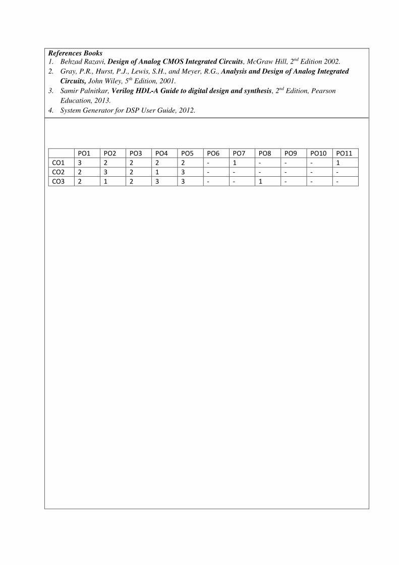
References Books 1. Behzad Razavi, Design of Analog CMOS Integrated Circuits, McGraw Hill, 2nd Edition 2002.
2. Gray, P.R., Hurst, P.J., Lewis, S.H., and Meyer, R.G., Analysis and Design of Analog Integrated
Circuits, John Wiley, 5th Edition, 2001.
3. Samir Palnitkar, Verilog HDL-A Guide to digital design and synthesis, 2nd Edition, Pearson
Education, 2013.
4. System Generator for DSP User Guide, 2012.
PO1 PO2 PO3 PO4 PO5 PO6 PO7 PO8 PO9 PO10 PO11
CO1 3 2 2 2 2 - 1 - - - 1
CO2 2 3 2 1 3 - - - - - -
CO3 2 1 2 3 3 - - 1 - - -

16VLPE01 IMAGE AND VIDEO PROCESSING
(Common to Applied Electronics)
L
3
T
0
P
0
C
3
CORE/ ELECTIVE COURSE: Elective
PREREQUISITES:
Digital Signal Processing.
COURSE ASSESSMENT METHODS: Both continuous and semester-end assessment.
COURSE OBJECTIVES:
To gain knowledge on the basics of digital imaging.
To get exposure to various image processing techniques.
To get exposure to video processing.
COURSE OUTCOMES:
Upon completion of this course, the students will have:
CO1: Knowledge on the basics of digital imaging.
CO2: Exposure to various image processing techniques.
CO3: Exposure to video processing.
TOPICS COVERED:
DIGITAL IMAGE PROCESSING FUNDAMENTALS (9)
Image Processing Systems- Elements of visual perception- Image sensing and acquisition- Image
sampling and quantization. Pixel relationships- Statistical properties- Histogram, mean, Standard
deviation-. Color Image Fundamentals, Chromaticity diagram. Color models- Image file formats, Image
transforms, Discrete fourier transform- Discrete cosine transform- wavelet transform.
IMAGE ENHANCEMENT AND RESTORATION (9)
Enhancement in spatial domain- Basic gray level transforms- Histogram processing- Spatial Filtering-
Enhancement in frequency domain- Image restoration- Degradation model- Noise models- Spatial Filters-
Frequency domain filters.
IMAGE SEGMENTATION AND REPRESENTATION (9)
Detection of discontinuities- Point, Line and Edge detection- Gradient operators- Thresholding- Region
based segmentation- Representation schemes- Chain codes- Polygon approximation- Boundary
descriptors- Simple descriptors- Shape number- Fourier descriptors.
VIDEO FUNDAMENTALS (9)
Basic concepts and Terminology-Monochrome Analog video – Color in Video – Anlog video standards –
Digital video basics – Analog-to Digital conversion – Color representation and chroma sub sampling –
Digital video formats and standards Video sampling rate and standards conversion.

PO1 PO2 PO3 PO4 PO5 PO6 PO7 PO8 PO9 PO10 PO11
CO1 2 3 2 2 3 2 1 1 1 3 -
CO2 3 3 2 2 3 3 1 1 3 3 -
CO3 3 3 2 2 3 3 1 1 3 3 -
VIDEO OBJECT EXTRACTION (9)
Back ground subtraction – Frame difference – Static and dynamic background modeling – Optical flow
techniques – Handling occlusion – Scale and appearance changes – Shadow removal.
TOTAL: 45 PERIODS
Reference Books :
1. Rafael C. Gonzalez, Richard E. Woods, “Digital Image Processing”, Pearson Education, Inc.,
Second Edition, 2004.
2. Anil K. Jain, “Fundamentals of Digital Image Processing”, Prentice Hall of India, 2002.
3. Oges Marques, “Practical Image and Video Processing Using MATLAB”, Wiley-IEEE Press,
2011.
4. A.Bovik, “Handbook of Image and Video processing”, 2nd Edition, Academic press, 2005.
5. Mark Nixon and Alberto Aguado, “Feature Extraction and Image Processing”, Academic Press,
2008.
6. Rafael C. Gonzalez, Richard E. Woods, Steven Eddins, “Digital Image Processing using
MATLAB”, Pearson Education, Inc., 2004.
7. Jayaraman S, Esakkirajan S and Veerakumar J, “Digital Image Processing”, Tata McGraw Hill
Education pvt ltd, 2010.

16VLPE02 MIXED SIGNAL CIRCUITS AND INTERFACING
(Common to Applied Electronics)
L
3
T
0
P
0
C
3
CORE/ ELECTIVE COURSE: Core
PREREQUISITES:
A-D & D-A Converters.
COURSE ASSESSMENT METHODS: Both continuous and semester-end assessment.
COURSE OBJECTIVES:
To gain basic knowledge on Sample and Hold Architecture.
To acquire knowledge on various A-D & D-A converters Architecture.
To gain Knowledge on Building Blocks & Precision Techniques.
COURSE OUTCOMES:
Upon completion of this course the students will have:
CO 1: basic knowledge on Sample and Hold Architecture.
CO 2: knowledge on various A-D & D-A converters Architecture.
CO 3: Knowledge on Building Blocks & Precision Techniques.
TOPICS COVERED:
SAMPLE-AND-HOLD ARCHITECTURES (9)
Introduction to Data conversion and Processing- Sampling Switches-MOS, Diode Switches-
Improvements in MOS Switch Performance-Conventional Open-Loop and Closed-Loop Architecture,
Open-Loop Architecture with Miller Capacitance, Multiplexed-Input Architectures, Recycling
Architecture, Switched-Capacitor Architecture, Current-Mode Architecture.
DIGITAL-TO-ANALOG CONVERTER ARCHITECTURES (9)
Basic principles-General Considerations-Performance Metrics-Reference Multiplication and Division-
Switching and Logical Functions in DACs-Resistor-Ladder DAC Architectures, Current-Steering
Architectures.
ANALOG-TO-DIGITAL CONVERTER ARCHITECTURES (9)
General Considerations- Performance Metrics- Flash Architectures, Two-Step Architectures,
Interpolative and Folding Architectures, Pipelined Architectures, Successive Approximation
Architectures, Interleaved Architectures.
BUILDING BLOCKS OF DATA CONVERSION SYSTEMS (9)
Amplifiers- Open-Loop Amplifiers, Closed-Loop Amplifiers, Operational Amplifiers, Gain Boosting
Techniques, Common-Mode Feedback. Comparators- Bipolar Comparators, CMOS Comparators,

BiCMOS Comparators.
PRECISION TECHNIQUES (9)
Comparator Offset Cancellation- Input, Output and multistage Offset Storage, Comparators Using Offset-
Cancelled Latches- Op Amp Offset Cancellation- Calibration Techniques- DAC and ADC Calibration
Techniques.
TOTAL: 45 PERIODS
Reference Books:
1. BehzadRazavi,“PrinciplesofDataConversionSystemDesign”, JohnWiley&Sons,2011.
2. SundaramNatarajan,“MicroelectronicsAnalysis&design”,McGrawHill2006.
3. R.JBaker,“CMOSMixedSignalCircuitDesign”,WileyInterscience,2nd Edition,2009.
4. B.Razavi,“DesignofAnalogCMOSIntegratedCircuits”,McGrawHill,2005.
5. DavidA. Johns and Ken Martin, “Analog Integrated Circuit Design”,WileyIndia,2008.
PO1 PO2 PO3 PO4 PO5 PO6 PO7 PO8 PO9 PO10 PO11
CO1 3 1 2 2 2 - 2 1 1 2 2
CO2 3 - 2 - - - - - - - -
CO3 3 3 1 - 2 - 1 - 1 - -

16VLPE03 RF SYSTEM DESIGN
(Common to Applied Electronics)
L
3
T
0
P
0
C
3
CORE/ ELECTIVE COURSE: Elective
PREREQUISITES:
Transmission Lines,RF System.
COURSE ASSESSMENT METHODS: Both continuous and semester-end assessment.
COURSE OBJECTIVES:
To gain knowledge on issues in designing RFIC and concepts of transistors.
To gain knowledge on integrated circuits design using Passive components.
To gain knowledge on RF Amplifiers and RF Mixers designs.
COURSE OUTCOMES:
Upon completion of this course, the students will have:
CO1 : Detailed Knowledge on issues in designing RFIC and concepts of transistors.
CO2 : Ability to design integrated circuits using Passive components.
CO3 : Detailed Knowledge on RF Amplifiers and RF Mixers designs.
TOPICS COVERED:
ISSUES IN RFIC DESIGN, NOISE, LINEARITY, and FILTERING: (9)
Lower frequency analog design and microwave design versus radio frequency integrated circuit design -
Impedance levels for microwave and low-frequency analog design- noise - linearity and distortion in RF
Circuits - dynamic range - filtering issue.
REVIEW OF TECHNOLOGY : (9)
Small -signal model of bipolar transistor - high frequency effects - noise in bipolar transistors - base shot
noise-noise sources in the transistor model - bipolar transistor design considerations-CMOS transistor.-
impedance matching - tapped capacitors and inductors - the concept of mutual inductance - tuning a
transformer - bandwidth of an impedance transformation network-quality factor of an LC resonator.
DESIGN OF PASSIVE CIRCUIT ELEMENTS IN IC TECHNOLOGIES: (9)
Technology backend and metallization in IC technologies - sheet resistance and skin effect -parasitic
capacitance and inductance -current handling in metal lines-design of inductors and transformers -
characterization of inductor-layout of spiral inductors - on-chip transmission lines - high frequency
measurements of on-chip passives and common De-Embedding techniques-packaging.
LNA AND POWER AMPLIFIER: (9)
Basic amplifiers - amplifiers with feedback - noise in amplifiers - linearity in amplifiers - differential pair
and other differential amplifiers-low-voltage topologies for LNAs and the use of on-chip transformers -
DC bias networks - temperature effects - broad band LNA design. Power amplifier: power capability -
efficiency calculations - matching considerations - Class A,B,C.D.E.F,G,H and S amplifiers -summary of
amplifier classes for RF Integrated circuits - AC load line - matching to achieve desired power -

PO1 PO2 PO3 PO4 PO5 PO6 PO7 PO8 PO9 PO10 PO11
CO1 3 - - - 1 1 1 1 - - 1
CO2 2 3 - - 1 - - 1 - - 1
CO3 1 - 1 1 1 1 - 1 1 - -
packaging -effects and implications of non linearity - linearization techniques - CMOS power amplifier
example.
MIXERS: (9)
Mixing with nonlinearity - basic mixer operation - controlled transconductance mixer - double-
balancedmixer - mixer with switching of upper quad - analysis of switching modulator-mixer noise -
linearity - improving isolation - image reject and single -sideband mixers-alternative mixer designs -
general design comments-CMOS mixers.
TOTAL:45 PERIODS
Reference Books:
1. John Rogers and Calvin Plett, “Radio Frequency Integrated Circuit Design”, Artech House, 2002.
2. Stephan A Mass, “Non-Linear Microwave and RF circuits”, Artech House.
3. Ferri Losee, “RF Systems, Components and Circuits handbook”, Artech house, 2002.
4. Larson LE, “RF and Microwave Circuit for Wireless Applications”, Artech House, 1997.

16VLPE04 MICROSENSORS AND MEMS
(Common to Applied Electronics)
L
3
T
0
P
0
C
3
CORE/ ELECTIVE COURSE: Elective
PREREQUISITES:
Basic science, Basic engineering.
COURSE ASSESSMENT METHODS: Both continuous and semester-end assessment.
COURSE OBJECTIVES:
To understand the microfabrication process, MEMS materials and various system issues.
To acquire basic knowledge on electrical and mechanical concepts of MEMS.
To acquire knowledge on various types of microsensors.
To introduce the concepts of optical and RF MEMS and various case studies.
COURSE OUTCOMES:
Upon completion of this course, the students will have: CO 1: Knowledge on microfabrication process, MEMS materials and various system
issues.
CO 2: Basic knowledge on electrical and mechanical concepts of MEMS.
CO 3: Knowledge on various types of microsensors.
CO 4: Introduction to optical and RF MEMS and various case studies.
TOPICS COVERED:
MICROFABRICATION AND MATERIALS (9)
Introduction – Evolution of MEMS – Microsensors and actuators – Microfabrication – Lithography,
Etching, Deposition, Oxidation, Diffusion - MEMS materials – Metals – Physical and chemical
properties, Metallization – Semiconductors – Electrical and chemical properties, Growth and Deposition
– Bulk and Surface micromachining.
ELECTRICAL AND MECHANICAL CONCEPTS (9)
Conductivity and resistivity – Elasticity – Stress and strain – Isotropic and Anisotropic materials –
Bending of beams – types, Deflection – Pure bending – Torsional deflections – intrinsic stress –
Resonance – Viscosity - Surface tension.
MEMS ISSUES AND CASE STUDIES (9)
Circuit and System issues – Electronics, Feedback systems and Noises. Case studies – Commercial
pressure sensor, MEMS magnetic actuators, Capacitive accelerometer.
TYPES OF MICROSENSORS (9)
Introduction – Thermal sensors, Radiation sensors, Mechanical sensors – Pressure microsensors and Flow
microsensors, Magnetic sensors, Bio(Chemical) sensors – SAW-IDT microsensor – fabrication –
applications – Strain, Temperature, Pressure and Humidity sensor.
OPTICAL AND RF MEMS (9)
Optical MEMS – Passive MEMS optical components – Lenses, Mirrors – Active actuators for optical
MEMS – Translation and rotation motion – RF MEMS – Basics - Sample case studies of optical and RF
MEMS.

PO1 PO2 PO3 PO4 PO5 PO6 PO7 PO8 PO9 PO10 PO11
CO1 3 - - - - - - - - - -
CO2 2 - - - - - - - - - -
CO3 3 - - - - - - - - - -
CO4 1 - - - - - - - 2 - -
TOTAL: 45 PERIODS
Reference Books:
1. Stephen Santuria,”Microsystems Design”, Kluwer publishers, 2000. 2. Julian w. Gardner, Vijay K. Varadan, Osama O. Awadelkarim, "Micro Sensors MEMS and Smart
Devices", John Wiley & Son LTD, 2002.
3. Chang Liu, "Foundations of MEMS", Pearson Education Inc., 2006.
4. Nadim Maluf,” An introduction to Micro electro mechanical system design”, Artech House, 2000.
5. Mohamed Gad-el-Hak, editor,”The MEMS Handbook”, CRC press Baco Raton, 2000. 6. Tai Ran Hsu,”MEMS & Micro systems Design and Manufacture” Tata McGraw Hill, New Delhi,
2002.
7. James J.Allen, "Micro Electro Mechanical System Design", CRC Press Publisher, 2010.

16VLPE05 GRAPH THEORY AND OPTIMIZATION TECHNIQUES
(Common to Applied Electronics)
L
3
T
0
P
0
C
3
CORE/ ELECTIVE COURSE: Elective
PREREQUISITES:
NIL
COURSE ASSESSMENT METHODS: Both continuous and semester-end assessment.
COURSE OBJECTIVES:
To solve problems in graphs and trees.
To implement the appropriate graph theoretic algorithms for the given problem.
To solve the optimization problem using linear and non-linear programming.
COURSE OUTCOMES:
Upon completion of this course the students will have: CO 1: An ability to solve problems in graphs and trees.
CO 2: An ability to apply graph theoretic algorithms for the given problem.
CO 3: An ability to solve the optimization problem using linear and non-linear programming.
TOPICS COVERED:
GRAPHS AND TREES (9)
Basic definitions and examples of graph - Subgraphs – Isomorphism - Operations on Graphs –
Hamiltonian path and Euler graph - Connectivity – Matrix representation of graphs – Directed graphs
Trees – properties of trees – Spanning tree.
GRAPH COLORING (9)
Planar graphs – Different representation, Graph duality – Geometric dual and Combinatorial dual - Graph
coloring – Chromatic number - Chromatic partitioning – Coverings – Matchings - Four color problem –
Regularization of a planar graph.
GRAPH THEORETIC ALGORITHMS (9)
Computer representation of a graph - Some basic algorithms for graph – Shortest path algorithms for
specified vertex to another vertex and all pairs of vertices – Minimal spanning tree algorithm – Kruskal
and Prim’s algorithm – Depth first and breadth first search algorithms..
CLASSICAL OPTIMIZATION AND LINEAR PROGRAMMING (9)
Single variable optimization – Multivariable optimization with various constraints – Lagrange’s method, Kuhn-Tucker condition – Linear Programming – Simplex method – Unbounded and infinite number of
solutions – Duality in linear programming – Transportation problem
NON-LINEAR PROGRAMMING (9)
Elimination methods – Unrestricted search, Fibonacci method, Golden section method – Unconstrained
minimization – Direct search methods - Random search methods and Grid search methods, Indirect
search methods – Steepest descent method and conjugate gradient method.
TOTAL: 45 PERIODS

PO1 PO2 PO3 PO4 PO5 PO6 PO7 PO8 PO9 PO10 PO11
CO1 1 3 1 - - - - - - - -
CO2 - 2 1 - - - - - - - -
CO3 1 2 2 - - - - - - - -
ReferenceBooks: 1. Narsingh Deo, “Graph Theory with Applications to Engineering and Computer Science,” PHI,
2004.
2. Rao S.S., “Engineering Optimizations: Theory and Practice”, New Age International Pvt. Ltd.,
4th Edition, 2009.
3. Douglas B. West, “Introduction to Graph Theory”, Prentice Hall of India, 2001. 4. Robin J. Wilson, “Introduction to Graph Theory”, Pearson Education 4th edition, 2007.
5. Kalyanmoy Deb, “Optimization for Engineering Design – Algorithms and Design”, PHI, 2012.
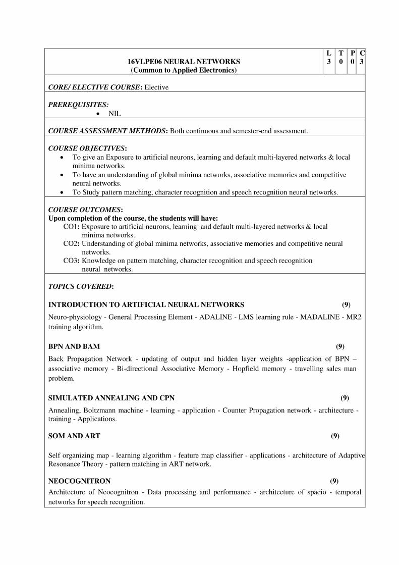
16VLPE06 NEURAL NETWORKS
(Common to Applied Electronics)
L
3
T
0
P
0
C
3
CORE/ ELECTIVE COURSE: Elective
PREREQUISITES:
NIL
COURSE ASSESSMENT METHODS: Both continuous and semester-end assessment.
COURSE OBJECTIVES:
To give an Exposure to artificial neurons, learning and default multi-layered networks & local
minima networks.
To have an understanding of global minima networks, associative memories and competitive
neural networks.
To Study pattern matching, character recognition and speech recognition neural networks.
COURSE OUTCOMES:
Upon completion of the course, the students will have: CO1: Exposure to artificial neurons, learning and default multi-layered networks & local
minima networks.
CO2: Understanding of global minima networks, associative memories and competitive neural
networks.
CO3: Knowledge on pattern matching, character recognition and speech recognition
neural networks.
TOPICS COVERED:
INTRODUCTION TO ARTIFICIAL NEURAL NETWORKS (9)
Neuro-physiology - General Processing Element - ADALINE - LMS learning rule - MADALINE - MR2
training algorithm.
BPN AND BAM (9)
Back Propagation Network - updating of output and hidden layer weights -application of BPN –
associative memory - Bi-directional Associative Memory - Hopfield memory - travelling sales man
problem.
SIMULATED ANNEALING AND CPN (9)
Annealing, Boltzmann machine - learning - application - Counter Propagation network - architecture -
training - Applications.
SOM AND ART (9)
Self organizing map - learning algorithm - feature map classifier - applications - architecture of Adaptive
Resonance Theory - pattern matching in ART network.
NEOCOGNITRON (9)
Architecture of Neocognitron - Data processing and performance - architecture of spacio - temporal
networks for speech recognition.

TOTAL:45 PERIODS
Reference Books:
1. J.A. Freeman and B.M.Skapura , "Neural Networks, Algorithms Applications and
ProgrammingTechniques", Pearson 2011.
2. Laurene Fausett, "Fundamentals of Neural Networks: Architecture, Algorithms
andApplications",Pearson education India 2006.
3. Simon Haykin, “Neural Networks & Learning Machines” third edition Pearson Education 2011.
PO1 PO2 PO3 PO4 PO5 PO6 PO7 PO8 PO9 PO10 PO11
CO1 3 2 - 2 2 - - - - - -
CO2 3 2 - 2 2 - - - - - -
CO3 3 3 - 2 2 - - - - - -

16VLPE07 ELECTRONIC PACKAGING TECHNOLOGIES
(Common to Applied Electronics)
L
3
T
0
P
0
C
3
CORE/ ELECTIVE COURSE: Elective
PREREQUISITES:
NIL
COURSE ASSESSMENT METHODS: Both continuous and semester-end assessment.
COURSE OBJECTIVES:
To Exposure on IC Packaging with the associated issues like thermal, speed, signal and integrity
power etc.
To Knowledge on the appropriate packaging styles and design procedures .
To Knowledge on CAD used in designing wiring boards.
COURSE OUTCOMES:
Upon completion of the course students will have CO1: Exposure on IC Packaging with associated issues like thermal, speed, signal and
integrity power etc.
CO2: Knowledge on the appropriate packaging styles and design procedures.
CO3: Knowledge on CAD used in designing wiring boards.
TOPICS COVERED:
OVERVIEW OF ELECTRONIC SYSTEMS PACKAGING (9)
Introduction of an Electronic system and history of semiconductors - Products and levels of packaging -
Packaging aspects of handheld products - Definition of PWB - Basics of Semiconductor and Process
flowchart - Wafer fabrication, inspection and testing - Wafer packaging; Packaging evolution; Chip
connection choices, Wire bonding - TAB and flip chip.
SEMICONDUCTOR PACKAGES (9)
Single chip packages or modules (SCM) - Commonly used packages and advanced packages - Materials in
packages; Thermal mismatch in packages; Multichip modules (MCM)-types; System-in-package (SIP);
Packaging roadmaps; Hybrid circuits; Electrical Design considerations in systems packaging, Resistive,
Capacitive and Inductive Parasitics - Layout guidelines and the Reflection problem - Interconnection.
CAD FOR PRINTED WIRING BOARDS (9)
Benefits from CAD; Introduction to DFM, DFR & DFT, Components of a CAD package and its highlights -
Beginning a circuit design with schematic work and component, layout, DFM check, list and design rules;
Design for Reliability, Printed Wiring Board Technologies: Board-level packaging aspects, Review of CAD
output files for PCB fabrication; Photo plotting and mask generation, Process flow-chart; Vias; PWB
substrates; Surface preparation, Photoresist and application methods; UV exposure and developing; Printing
technologies for PWBs, PWB etching; PWB etching; Resist stripping; Screen-printing technology, through-
hole manufacture process steps; Panel and pattern plating methods, Solder mask for PWBs; Multilayer
PWBs; Introduction to, microvias, Microvia technology and Sequential build-up technology process flow for
high-density, interconnects.

SURFACE MOUNT TECHNOLOGY AND THERMAL CONSIDERATIONS (9)
SMD benefits; Design issues; Introduction to soldering, Reflow and Wave Soldering methods to attach
SMDs, Solders; Wetting of solders; Flux and its properties; Defects in wave soldering, Vapour phase
soldering, BGA soldering and De-soldering/Repair; SMT failures, SMT failure library and Tin Whisker, Tin-
lead and lead-free solders; Phase diagrams; Thermal profiles for reflow soldering; Lead freevAlloys, Lead-
free solder considerations; Green electronics; RoHS compliance and e-waste recycling, Issues, Thermal
Design considerations in systems packaging (L. Umanand, Thermal Design considerations in systems
packaging.
EMBEDDED PASSIVES TECHNOLOGY (9)
Introduction to embedded passives - Need for embedded passives - Design Library; Embedded resistor
processes - Embedded capacitors - Processes for embedding capacitors.
TOTAL: 45 PERIODS
Reference Books:
1. Tummala, Rao R., Fundamentals of Microsystems Packaging, McGraw Hill Reference Book 2001.
2. Blackwell (Ed), The electronic packaging handbook, CRC Press1999.
3. Tummala, Rao R, Microelectronics packaging handbook, McGraw Hill 1997.
4. Bosshart, Printed Circuit Boards Design and Technology, Tata McGraw Hill 2002.
5. William D. Brown, “Advanced Electronic Packaging”, IEEE Press, 1999.
PO1 PO2 PO3 PO4 PO5 PO6 PO7 PO8 PO9 PO10 PO11
CO1 2 1 1 2 2 1 2 2 - - 1
CO2 2 1 1 2 2 - 2 2 - - 1
CO3 1 1 1 2 3 - 3 1 - - 1

16VLPE08 NANO ELECTRONICS
(Common to Applied Electronics)
L
3
T
0
P
0
C
3
CORE/ ELECTIVE COURSE: Elective
PREREQUISITES:
Semiconductor theory.
COURSE ASSESSMENT METHODS: Both continuous and semester-end assessment.
COURSE OBJECTIVES:
To gain knowledge in particles, waves and materials for Nano Electronics.
To understand growth, fabrication and measurement techniques for nanostructures.
To gain knowledge on Nano Structure and Devices.
COURSE OUTCOMES:
Upon completion of this course the students will have:
CO 1: Depth knowledge in particles, waves and materials for Nano Electronics.
CO 2: An ability to understand growth, fabrication and measurement techniques for
nanostructures.
CO3: Knowledge on Nano Structure and Devices.
TOPICS COVERED:
PARTICLES, WAVES AND WAVE MECHANICS (9)
Introduction -Classical particles -Classical waves -Wave–particle duality -Wave mechanics-The
Schrodinger wave equation-Wave mechanics of particles-Atoms and atomic orbitals.
MATERIALS FOR NANO ELECTRONICS
(9)
Introduction -Semiconductors -Crystal lattices: bonding in crystals -Electron energy bands -
Semiconductor heterostructures - Lattice-matched and pseudomorphic heterostructures - Organic
semiconductors -Carbon nonmaterial: nanotubes and fullerenes.
GROWTH, FABRICATIONAND MEASUREMENT TECHNIQUES FOR NANO STRUCTURES
(9)
Bulk crystal and heterostructure growth -Nanolithography, etching, and other means for fabrication of
nanostructures and nanodevices -Techniques for characterization of nanostructures -Spontaneous
formation and ordering of nanostructures -Clusters and nanocrystals -Methods of nanotube growth -
Chemical and biological methods for nanoscale fabrication -Fabrication of nanoelectromechanical
systems.
ELECTRON TRANSPORT IN SEMICONDUCTORS AND NANOSTRUCTURES (9)
Time and length scales of the electrons in solids -Statistics of the electrons in solids and nanostructures -
The density of states of electrons in nanostructures -Electron transport in nanostructures. Electrons in
traditional low-dimensional structures- Electrons in quantum wells -Electrons in quantum wires -
Electrons in quantum dots.
NANOSTRUCTURE DEVICE (9) Resonant-tunneling diodes - Field-effect transistors -Single-electron-transfer devices -Potential-effect
transistors -Light-emitting diodes and lasers -Nanoelectromechanical system devices -dot cellular
automata.

PO1 PO2 PO3 PO4 PO5 PO6 PO7 PO8 PO9 PO10 PO11
CO1 3 1 2 1 3 2 - 1 1 - 1
CO2 2 2 1 1 2 - 2 - 1 1 2
CO3 1 1 3 2 2 1 - 1 1 - 1
TOTAL: 45 PERIODS
Reference Books: 1. Vladimir V. Mitin, Viatcheslav A. Kochelap, Michael A. Stroscio, “Introduction to Nan electronics:
Science, Nanotechnology, Engineering, and Applications”, Cambridge University Press 2011.
2. Supriyo Datta,“Lessonsfrom Nanoelectronics: A New Perspective on Transport”, World Scientific 2012.
3. George W. Hanson, “Fundamentals of Nanoelectronics”, Pearson 2009.
4. Mircea Dragoman, Daniela Dragoman, “Nanoelectronics: principles and devices”, CRC Press 2006.
5. Karl Goser, Peter Glösekötter, Jan Dienstuhl,“Nanoelectronics and Nanosystems: From
Transistors to Molecular and Quantum Devices“, Springer 2004.
6. Mark A. Reed, Takhee Lee, “Molecular nanoelectronics”, American Scientific Publishers 2003.
7. Jaap Hoekstra, “Introduction to Nan electronic Single-Electron Circuit Design”, Pan Stanford Publishing 2010.
8. W. Ranier,“Nano Electronics and Information Technology”, John Wiley & Sons 2012.

16VLPE09 REAL TIME OPERATING SYSTEM
(Common to Applied Electronics)
L
3
T
0
P
0
C
3
CORE/ ELECTIVE COURSE: Elective
PREREQUISITES:
Operating System.
COURSE ASSESSMENT METHODS: Both continuous and semester-end assessment..
COURSE OBJECTIVES:
To learn issues related to the design and analysis of systems with real time Constraints and
features of Real time OS.
To learn about various Uniprocessor and Multiprocessor scheduling mechanisms.
To get knowledge on real time communication protocols.
COURSE OUTCOMES:
Upon completion of this course, the students will have: CO1: Knowledge on issues related to the design and analysis of systems with real time
Constraints and features of Real time OS.
CO2: Ability to analyze various Uniprocessor and multiprocessor scheduling mechanism.
CO3: Knowledge on real time communication protocols.
TOPICS COVERED:
INTRODUCTION TO REAL TIME OPERATING SYSTEM (9)
Introduction to Real time computing Concepts; Example of real time applications-Structure of a real time
system-Characterization of real time systems and tasks- Hard and Soft timing constraints -Design
challenges- Performance metrics -Prediction of Execution time: Source code analysis, Micro -architecture
level analysis, Cache and pipeline issues -Programming Languages for Real -Time System.
REVIEW OF RTOS (9)
Real time OS-Threads and Tasks-Structure of Microkernel-Time services-Scheduling Mechanisms
Communication and Synchronization-Event Notification and Software interrupt.
TASK SCHEDULING AND ALGORITHMS (9)
Task assignment and Scheduling -Task allocation algorithms- Single processor and Multiprocessor task
scheduling- Clock driven and Priority based scheduling algorithms -Fault tolerant Scheduling.
REAL TIME PROTOCOLS (9)
Real Time Communication Network-Topologies and architecture issues-protocols-contension based,
token based, polled bus, deadline based protocol, Fault tolerant routing.RTP and RTCP.
REAL TIME DATABASES (9)
Real time Databases-Transaction priorities-Concurrency control issues-Disk scheduling algorithms-Two
phase approach to improve predictability.
TOTAL : 45 PERIODS

PO1 PO2 PO3 PO4 PO5 PO6 PO7 PO8 PO9 PO10 PO11
CO1 3 3 2 2 2 2 - 1 2 2 -
CO2 3 3 2 2 2 2 - 1 2 3 -
CO3 3 3 2 2 2 2 - 1 2 2 -
Reference Books:
1. Jane W.S. Liu, Real Time Operating Systems, Pearson Education India, 2000.
2. Philip A. Laplante and Seppo J. Ovaska, “Real Time Operating Systems Design and Analysis: Tools
for the Practitioner’’ IV Edition IEEE Press, Wiley,2013.
3. C.M. Krishna, Kang G. Shin – “ Real Time Operating Systems”, International Edition, McGraw Hill Companies, Inc., New York, 2013.

16VLPE10 EMBEDDED CONTROLLERS
L
3
T
0
P
0
C
3
CORE/ ELECTIVE COURSE: Elective
PREREQUISITES:
NIL
COURSE ASSESSMENT METHODS: Both continuous and semester-end assessment.
COURSE OBJECTIVES: • To learn about the designing of an embedded system for commercial applications.
• To learn the features, architecture and programming of PIC microcontrollers.
• To learn the features, architecture and programming of MSP430 microcontrollers.
• Interfacing Input/output devices with the PIC and MSP430 microcontroller.
COURSE OUTCOMES:
Upon completion of this course, the students will have: CO1:Ability to design and develop embedded systems for a given problem.
CO2:Ability to develop embedded system for entertainment, communication and medical applications.
CO3:Ability build and trouble shoot embedded systems.
TOPICS COVERED:
8-BIT CONTROLLER (9)
Microprocessors and microcontrollers, introducing PIC 16F877- architecture, memory technologies, timing
circuits, power-up and reset, parallel ports, ADC, interrupt, serial peripheral buses (UART, I2C, SPI), PWM,
counters and timers, instruction set and assembly language programming.
PIC DEVELOPMENT TOOLS AND PROGRAMMING (9)
Software development tools- editor, assembler, compiler, cross-compiler and simulator, Hardware
development tools- development board, device programmer, in-circuit emulator and debuggers.
Embedded C Programming, data types and variables, data type modifiers, storage Class modifiers, C
statements, structures and operations, pointers, libraries, in-line assembly programming, optimizing and
testing embedded C programs.
PERIPHERAL INTERFACING WITH PIC MICROCONTROLLER (9)
Human and physical interfaces- switches to keyboard, LED display, liquid crystal display, Actuators and
sensors, PWM, serial communication protocols (UART, I2C, SPI), programming interrupt, timers and
counter.
16-BIT CONTROLLER (9)
MSP430 – Introduction to Architecture - Embedded C Programming in MSP430 – GPIO Pins &
Configuration Timers, Capture, & PWM DAC- ADCs –Memory System-Flash Memory-DMA.
MSP 430 Interfacing (9)
USCI Port –SPI mode - I2C Mode-UART Mode & RS232 Low Power Mode Operation- Interfacing- Input
Devices-Output Devices-DC Motor-Stepper Motor- Alarm interface- AC Devices.
TOTAL: 45 PERIODS

PO1 PO2 PO3 PO4 PO5 PO6 PO7 PO8 PO9 PO10 PO11
CO1 2 - 2 - 1 - - - 2 - -
CO2 1 - 3 - 2 - - - 2 - -
CO3 - - - 2 2 1 1 - - - 3
Reference Books:
1. Kirk Zurell, "C programming for Embedded Systems", CRC Press, 2000.
2. Dogan Ibrahim, "Advanced PIC microcontroller projects in C", Newnes publication, 2012.
3. Tim Wilmshurst, "Designing Embedded Systems with PIC microcontrollers-Principles and
Applications", Newnes Publications, 2007.
4. Muhammad Ali Mazidi, Rolin McKinlay, Danny Causey, "PIC Microcontroller and Embedded Systems:
Using Assembly and C for PIC18", Prentice hall publications, 2007.
5. Martin Bates, "Interfacing PIC microcontrollers-Embedded Design by Interactive Simulation", Newnes
Publication, 2006.
6. John H. Davies“MSP430 Microcontrollers Basics”, Elsevier Limited 2008. 7. Steven Barrett, Daniel Pack ,”Microcontroller Programming and Interfacing TI MSP430, Part 1”,
Morgan and Claypool,2011.

16VLPE11 HIGH PERFORMANCE COMPUTER NETWORKS
L
3
T
0
P
0
C
3
CORE/ ELECTIVE COURSE: Elective
PREREQUISITE
Knowledge in Computer Networks
COURSE ASSESSMENT METHODS: Both continuous and semester-end assessment
COURSE OBJECTIVES:
To ensure a comprehensive understanding of high speed computer network architectures
To study mathematical models related to network performance analysis.
To focus on current and emerging networking Technologies.
COURSE OUTCOMES:
The upon completion of this course students will have ability:
CO1:To design and implement network protocols in HPCN.
CO2:To analyze performance of network related issues using mathematical models.
CO3:To compare the various methods of providing connection-oriented services over
an advanced network with reference to MPLS, VPN.
TOPICS COVERED:
SWITCHING NETWORKS (9)
Switching – Packet switching - Ethernet, Token Ring, FDDI, DQDB, Frame Relay, SMDS, Circuit Switched
– SONET, DWDM, DSL, Intelligent Networks – CATV, ATM – Features, Addressing Signaling & Routing,
Header Structure, ATM Adaptation layer, Management control, BISDN, Internetworking with ATM.
MULTIMEDIA NETWORKING APPLICATIONS (9)
Streaming stored Audio and Video, Best effort service, protocols for real time interactive applications,
Beyond best effort, scheduling and policing mechanism, integrated services, RSVP- differentiated services.
ADVANCED NETWORKS CONCEPTS (9)
VPN-Remote-Access VPN, site-to-site VPN, Tunneling to PPP, Security in VPN.MPLS-operation, Routing,
Tunneling and use of FEC, Traffic Engineering, and MPLS based VPN, overlay networks-P2P connections.-
IPv4 vs V6.
PACKET QUEUES AND DELAY ANALYSIS (9)
Little‟s theorem, Birth and Death process, queueing discipline- Control & stability -, Markovian FIFO
queueing system, Non-markovian - Pollaczek-Khinchin formula and M/G/1, M/D/1, self-similar models and
Batch-arrival model, Networks of Queues – Burke‟s theorem and Jackson Theorem.
NETWORK SECURITY AND MANAGEMENT (9)
Principles of cryptography – Elliptic-AES- Authentication – integrity – key distribution and certification –
Access control and: fire walls – DoS-attacks and counter measures – security in many layers. Infrastructure
for network management – The internet standard management framework – SMI, MIB, SNMP, Security and
administration – ASN.1.

PO1 PO2 PO3 PO4 PO5 PO6 PO7 PO8 PO9 PO10 PO11
CO1 1 - 3 - - 1 - - 2 - -
CO2 1 - - - 3 - - - 2 - -
CO3 - - - 2 - - - 1 1 - -
TOTAL: 45 PERIODS
Reference Books:
1. Aunurag Kumar, D. Manjunath, Joy Kuri, “Communication Networking”, Morgan Kaufmann Publishers, 2011.
2. J.F. Kurose & K.W. Ross, “Computer Networking- A Top Down Approach Featuring the Internet”, Pearson Education, 2nd Edition, 2003.
3. Nader F.Mir, “Computer and Communication Networks”, Pearson Education, 2009. 4. Walrand .J. Varatya, “High Performance Communication Network”, Morgan Kaufmann –
Harcourt Asia Pvt. Ltd., 2nd Edition, 2000.
5. Hersent Gurle & Petit, “IP Telephony, Packet Pored Multimedia Communication Systems”, Pearson Education 2003.
6. Fred Halsall and Lingana Gouda Kulkarni, “Computer Networking and the Internet”, Fifth Edition, Pearson Education, 2012.
7. Larry L.Peterson & Bruce S.David, “Computer Networks: A System Approach”- Morgan Kaufmann
Publisher, 1996.

16VLPE12 ANALYSIS AND DESIGN OF ANALOG INTEGRATED CIRCUITS
L
3
T
0
P
0
C
3
CORE/ ELECTIVE COURSE: Core
PREREQUISITES:
Analog integrated circuits.
COURSE ASSESSMENT METHODS: Both continuous and semester-end assessment.
COURSE OBJECTIVES:
To acquire knowledge on circuit configuration for linear integrated circuits and multiple
transistor amplifier.
To analyze nonlinear analog circuits.
To analyze and design Operational amplifier.
COURSE OUTCOMES:
Upon completion of this course, the students will have: CO1: Knowledge on circuit configuration for linear integrated circuits and multiple transistor
amplifiers.
CO2: Ability to analyze nonlinear analog circuits.
CO3: Ability to analyze and design Operational amplifier.
TOPICS COVERED:
CIRCUIT CONFIGURATION FOR LINEAR IC (9)
Current Sources-General Properties-Simple Current Mirror with beta helper-Simple current mirror with
degeneration-Cascode Current Mirror-Wilson Current MIRROR- Widlar current source-Supply
Insensitive Biasing-Temperature Insensitive Biasing. Output Stages - Emitter and source followers, Push
pull output stages.
SINGLE TRANSISTOR AND MULTIPLE TRANSISTOR AMPLIFIER (9)
Basic single transistor amplifier stages -CE, CB, CC configuration- Multiple transistor amplifier stage –active cascode configuration, differential pairs – Emitter coupled pair.
OPERATIONAL AMPLIFIER (9)
Analysis of operational amplifier circuit, Slew rate model and High Frequency Analysis - Operational
Amplifier noise.
NON LINEAR ANALOG CIRCUITS (9)
Precision Rectification-Analysis of four quadrant and variable trans conductance multiplier-Application
of Gilbert cell. Balanced Modulator - Closed loop analysis of PLL - Voltage Controlled Oscillator.
ANALOG DESIGN WITH MOS TECHNOLOGY (9)
MOS Current Mirror-Simple, Cascode, Widlar and Wilson Current source-MOS Supply Insensitive
Biasing. MOS amplifier, source coupled pair and basic two stage MOS opamps.
TOTAL:45 PERIODS

Reference Books:
1.Schaumount, Patrick, “A Practical Introduction to Hardware/ Software Co-Design”,2013.
2.Ralf Niemann, “Hardware/Software Co-Design for Data Flow Dominated Embedded Systems”,
Kluwer Academic Pub, 2015.
3.Jorgen Staunstrup, Wayne Wolf, ”Hardware/Software Co-Design: Principles and Practice”, Kluwer Academic Pub, 2015.
4.Giovanni De Micheli, Rolf Ernst Morgon,” Reading in Hardware/Software Co-Design“
Kaufmann Publishers, 2001.
PO1 PO2 PO3 PO4 PO5 PO6 PO7 PO8 PO9 PO10 PO11
CO1 3 2 2 2 2 2 - 1 2 1 -
CO2 3 2 2 2 2 2 - 1 2 1 -
CO3 3 2 2 2 2 2 - 1 2 1 -

16VLPE13 DSP INTEGRATED CIRCUITS
L
3
T
0
P
0
C
3
CORE/ ELECTIVE COURSE: Elective
PREREQUISITES:
Digital Signal Processing.
COURSE ASSESSMENT METHODS: Both continuous and semester-end assessment.
COURSE OBJECTIVES:
To gain Basic knowledge of Digital Signal Processing, Discrete Time Transforms and VLSI circuit
technologies.
To get exposure to digital filters, multi rate signal processing and finite word length effects.
To Understand the principle of state of art DSP architectures and design of arithmetic units.
COURSE OUTCOMES:
Upon completion of the course students will have
CO1: Basic knowledge of Digital Signal Processing, Discrete Time Transforms and VLSI circuit
technologies.
CO2: Exposure to digital filters, multi rate signal processing and finite word length effects.
CO3: Understanding of the principle of state of art DSP architectures and design of
arithmetic units.
TOPICS COVERED:
NUMBERS SYSTEMS, ARITHMATIC UNITS AND INTEGRATED CIRCUITS (9)
Conventional number system - Redundant Number system - Residue Number System .Bit-parallel and Bit-
Serial arithmetic - Distributed Arithmetic - Basic shift accumulator - Reducing the memory size - Complex
multipliers - Improved shift-Accumulator.
DIGITAL SIGNAL PROCESSING (9)
Digital signal processing - Sampling of analog signals - Selection of sample frequency - Signal-processing
systems - Frequency response - Transfer functions - Signal flow graphs - Filter structures - Adaptive DSP
algorithms - FFT-The Fast Fourier Transform Algorithm - Image coding - Discrete cosine transforms.
DIGITAL FILTERS AND FINITE WORD LENGTH EFFECTS (9)
FIR filters - FIR filter structures - FIR chips - IIR filters - Specifications of IIR filters - Multirate systems -
Interpolation with an integer factor L - Sampling rate change with a ratio L/M - Multirate filters. Finite word
length effects -Parasitic oscillations - Scaling of signal levels - Round-off noise - Measuring round-off noise -
Coefficient sensitivity - Sensitivity and noise.
DSP INTEGRATED CIRCUITS AND VLSI CIRCUIT TEHNOLOGIES (9)
Standard digital signal processors - Application specific IC’s for DSP - DSP systems - DSP system design -
Integrated circuit design. MOS transistor - MOS logic - VLSI process technologies - Trends in CMOS
technologies.
DSP ARCHITECTURES AND SYNTHESIS (9)
DSP system architectures - Standard and Ideal DSP architecture - Multiprocessors and multi computers -

PO1 PO2 PO3 PO4 PO5 PO6 PO7 PO8 PO9 PO10 PO11
CO1 3 2 - 2 2 - - - - - -
CO2 3 2 - 2 2 - - - - - -
CO3 3 2 - 2 3 - - - - - -
Systolic and Wave front arrays - Mapping of DSP algorithms onto hardware - Implementation based on
complex PEs - Shared memory architecture with Bit – serial PEs - Layout of VLSI circuits - FFT processor -
DCT processor and Interpolator as case studies.
TOTAL: 45 PERIODS
Reference Books
1. Lars Wanhammer, “DSP Integrated Circuits”, Academic press, New York 2001. 2. A.V.Oppenheim et.al, “Discrete-time Signal Processing”, Pearson education, 2014.
3. Emmanuel C. Ifeachor, Barrie W. Jervis, “Digital signal processing–A practical approach”, 2ndedition, Harlow Prentice Hall, 2011. 4. Keshab K.Parhi, „VLSI digital Signal Processing Systems design and Implementation”, JohnWiley & Sons, 2007.

16VLPE14 HARDWARE SOFTWARE CO-DESIGN
L
3
T
0
P
0
C
3
CORE/ ELECTIVE COURSE: Elective
PREREQUISITES:
ASIC, Embedded Systems.
COURSE ASSESSMENT METHODS: Both continuous and semester-end assessmen.t
COURSE OBJECTIVES:
To study and compare the co-design approaches for single processor and multiprocessor
architectures.
To know the various techniques of prototyping and emulation.
To study the languages for system level specification and design
COURSE OUTCOMES:
Upon completion of the course, the students will have:
CO1:Knowledge on Co-design approaches for single processor and multiprocessor
Architectures.
CO2: Ability to apply the various techniques of prototyping and emulation.
CO3: Knowledge on the languages for system level specification and design.
TOPICS COVERED:
SYSTEM SPECIFICATION AND MODELLING (9)
Embedded Systems - Hardware/Software Co-Design, Co - Design for System Specification and
Modelling, Co - Design for Heterogeneous Implementation - Processor Synthesis - Single Processor
Architectures with single ASIC - Single Processor Architectures with many ASICs - Multi-Processor
Architectures - Comparison of Co-Design Approaches - Models of Computation - Requirements for
Embedded System Specification.
HARDWARE/SOFTWARE PARTITIONING (9)
The Hardware/Software Partitioning Problem - Hardware-Software Cost Estimation - Generation of the
Partitioning Graph - Formulation of the Hardware-Software Partitioning Problem – Optimization -
Hardware-Software Partitioning based on Heuristic Scheduling - Hardware-Software Partitioning based
on Genetic Algorithms.
HARDWARE/SOFTWARE CO-SYNTHESIS (9)
The Co-Synthesis Problem - State Transition Graph - Refinement and Controller Generation - Distributed
System Co-Synthesis.
PROTOTYPING AND EMULATION (9)
Introduction - Prototyping and Emulation Techniques - Prototyping and Emulation Environments - Future
Developments in Emulation and Prototyping - Target Architecture - Architecture Specialization
Techniques - System Communication Infrastructure - Target Architectures and Application System
Classes - Architectures for Control-Dominated Systems - Architectures for Data-Dominated Systems -
Mixed Systems and Less Specialized Systems.

DESIGN SPECIFICATION AND VERIFICATION (9)
Concurrency, Coordinating Concurrent Computations - Interfacing Components, Verification -
Languages for System-Level Specification and Design - System Level Specification - Design
Representation for System Level Synthesis - System Level Specification Languages - Heterogeneous
Specification and Multi-Language Co- simulation.
TOTAL:45 PERIODS
Reference Books:
1.Schaumount, Patrick, “A Practical Introduction to Hardware/ Software Co-Design”,2013.
2.Ralf Niemann, “Hardware/Software Co-Design for Data Flow Dominated Embedded Systems”, Kluwer Academic Pub, 2015.
3.Jorgen Staunstrup, Wayne Wolf, ”Hardware/Software Co-Design: Principles and Practice”, Kluwer Academic Pub, 2015.
4.Giovanni De Micheli, Rolf Ernst Morgon,” Reading in Hardware/Software Co-Design“
Kaufmann Publishers, 2001.
PO1 PO2 PO3 PO4 PO5 PO6 PO7 PO8 PO9 PO10 PO11
CO1 2 2 1 2 3 1 2 2 - - 1
CO2 2 2 1 3 3 1 3 2 - - 1
CO3 2 1 - 3 3 - 2 1 - - 1

16VLPE15 DESIGN OF SEMICONDUCTOR MEMORIES
L
3
T
0
P
0
C
3
CORE/ ELECTIVE COURSE: Elective
PREREQUISITES:
Computer Architecture, Digital System Design.
COURSE ASSESSMENT METHODS: Both continuous and semester-end assessment.
COURSE OBJECTIVES:
To study the architectures for SRAM and DRAM.
To know about various non-volatile memories.
To study the fault modeling and testing of memories for fault detection.
To learn the radiation hardening process and issues for memory.
COURSE OUTCOMES:
Upon completion of the course, the students will have: CO1: Knowledge on the architectures for SRAM, DRAM and various non-volatile memories.
CO2: Knowledge on fault modeling and testing of memories for fault detection.
CO3: Exposure on the radiation hardening process and issues for memory.
TOPICS COVERED:
RANDOM ACCESS MEMORY TECHNOLOGIES (9)
Static Random Access Memories (SRAMs): SRAM Cell Structures - MOS SRAM Architecture –MOS
SRAM Cell and Peripheral Circuit Operation - Bipolar SRAM Technologies - Silicon On Insulator (SOI)
Technology - Advanced SRAM Architectures and Technologies - Application Specific SRAMs. Dynamic
Random Access Memories (DRAMs): DRAM Technology Development - CMOS DRAMs-DRAMs Cell
Theory and Advanced Cell Structures - BiCMOS, DRAMs - Soft Error Failures in DRAMs - Advanced
DRAM Designs and Architecture - Application Specific DRAMs.
NON VOLATILE MEMORIES (9)
Masked Read-Only Memories (ROMs) - High Density ROMs - Programmable Read-Only Memories
(PROMs) - Bipolar PROMs - CMOS PROMs - Erasable (UV) - Programmable Read-Only Memories
(EPROMs) - Floating-Gate EPROM Cell-One-Time Programmable (OTP) EPROMs-Electrically
Erasable PROMs (EEPROMs) - EEPROM Technology and Architecture - Nonvolatile SRAM -Flash
Memories (EPROMs or EEPROM) - Advanced Flash Memory Architecture.
MEMORY FAULT MODELING, TESTING, MEMORY DESIGN FOR TESTABILITY AND
FAULT TOLERANCE (9)
RAM Fault Modeling, Electrical Testing, Pseudo Random Testing - Megabit DRAM Testing Nonvolatile
Memory Modeling and Testing - IDDQ Fault Modeling and Testing - Application Specific Memory
Testing. General Design for Testability Techniques – Ad Hoc Design Techniques, Structured Design
Techniques – RAM Built-In Self – Test (BIST).
RELIABILITY AND RADIATION EFFECTS (9)
General Reliability Issues - RAM Failure Modes and Mechanism - Nonvolatile Memory Reliability -
Reliability Modeling and Failure Rate Prediction - Design for Reliability - Reliability Test Structures -
Reliability Screening and Qualification. Radiation Effects - Single Event Phenomenon (SEP) - Radiation
Hardening Techniques Radiation Hardening Process and Design Issues - Radiation Hardened Memory

PO1 PO2 PO3 PO4 PO5 PO6 PO7 PO8 PO9 PO10 PO11
CO1 3 2 1 3 3 2 1 2 - - 1
CO2 3 2 - 3 3 2 - 2 - - 1
CO3 2 2 - 3 3 2 - 1 - - 1
Characteristics - Radiation Hardness Assurance and Testing – Radiation Dosimetry - Water Level
Radiation Testing and Test Structures.
PACKAGING TECHNOLOGIES (9)
Random Access Memories (MRAMs) - Experimental Memory Devices. Memory Hybrids and MCMs
(2D) - Memory Stacks and MCMs (3D) - Memory MCM Testing and Reliability Issues - Memory Cards
-High Density Memory Packaging Future Directions.
TOTAL: 45 PERIODS
Reference Books:
1. 1. Ashok K. Sharma, " Semiconductor Memories Technology, Testing and Reliability ",Prentice Hall of
2. India Private Limited, New Delhi,2003.
3. 2. Tegze P. Haraszti, “CMOS Memory Circuits”, Kluwer Academic publishers, 2002.
4. 3. Betty Prince, “ Emerging Memories: Technologies and Trends”, Kluwer Academic publishers,2002.

16VLPE16 SYSTEM ON CHIP
L
3
T
0
P
0
C
3
CORE/ ELECTIVE COURSE: Elective
PREREQUISITES:
Digital Electronics.
COURSE ASSESSMENT METHODS: Both continuous and semester-end assessment.
COURSE OBJECTIVES:
Ability to design combinational and sequential logic networks.
To gain knowledge on optimization of power in combinational and sequential logic machines.
Ability to design FPGA and PLA and Knowledge on floor planning methods for system
design.
COURSE OUTCOMES:
Upon completion of this course, the students will have: CO 1: Ability to design combinational and sequential logic networks.
CO 2: Knowledge on optimization of power in combinational and sequential logic machines.
CO 3: Ability to design FPGA and PLA and Knowledge on floor planning methods for system
design.
TOPICS COVERED:
LOGIC GATES (9)
Introduction. Combinational Logic Functions. Static Complementary Gates. Switch Logic. Alternative
Gate Circuits. Low-Power Gates. Delay Through Resistive Interconnect. Delay Through Inductive
Interconnect.
COMBINATIONAL LOGIC NETWORKS (9)
Introduction. Standard Cell-Based Layout. Simulation. Combinational Network Delay. Logic and
interconnect Design. Power Optimization. Switch Logic Networks. Combinational Logic Testing.
SEQUENTIAL MAC (9)
Introduction. Latches and Flip-Flops. Sequential Systems and Clocking Disciplines. SequentialSystem
Design. Power Optimization. Design Validation. Sequential Testing.
SUBSYSTEM DESIGN (9)
Introduction. Subsystem Design Principles. Combinational Shifters. Adders. ALUs. Multipliers. High-
Density Memory. FieldProgrammable Gate Arrays. Programmable Logic Arrays. References.Problems.
FLOOR-PLANNING (9)
Introduction, Floor-planning Methods – Block Placement & Channel Definition, Global
Routing,switchbox Routing, Power Distribution, Clock Distributions, Floor-planning Tips, Design
Validation. Off-Chip Connections – Packages, The I/O Architecture, PAD Design.
TOTAL:45 PERIODS

PO1 PO2 PO3 PO4 PO5 PO6 PO7 PO8 PO9 PO10 PO11
CO1 3 2 - 2 2 - - 1 - 1 -
CO2 3 2 - 2 2 - - 1 - 1 -
CO3 2 2 - 2 3 - - 1 - 1 -
Reference Books: 1. Wayne Wolf, “Modern VLSI Design – System – on – Chip Design”, Prentice Hall, 3rd Edition
2008.
2. Wayne Wolf, “Modern VLSI Design – IP based Design”, Prentice Hall, 4th Edition , 2008.

16VLPE17 RECONFIGURABLE ARCHITECTURE FOR VLSI
L
3
T
0
P
0
C
3
CORE/ ELECTIVE COURSE: Elective
PREREQUISITES:
VLSI design automation.
ASIC design.
COURSE ASSESSMENT METHODS: Both continuous and semester-end assessment.
COURSE OBJECTIVES:
To gain knowledge on run time computing and its applications to VLSI.
To learn optical reconfigurable models.
To understand various multi core architecture.
COURSE OUTCOMES:
Upon completion of this course the students will have ability to: CO1:gain knowledge on run time computing and its applications to VLSI.
CO2:learn optical reconfigurable models.
CO3:understand various multi core architectures.
TOPICS COVERED:
RECONFIGURABLE COMPUTING HARDWARE (9)
Logic- computational fabric, Array and interconnect-Extended logic Configuration-Reconfigurable
processing fabric architectures-RPF integration into traditional computing systems- operating system
support for reconfigurable computing- Evolvable FPGA.
MAPPING DESIGNS INTO RECONFIGURABLE PLATFORMS (9)
Structural mapping- integrated mapping- mapping for heterogeneous resources-Placement problem –
clustering- simulated annealing – partition based placement – analytical placement- partitioning for
granularity partitioning of parallel programs- instance specific design.
COMPUTATIONAL ARCHITECTURES FOR FPGA (9)
Precision analysis for fixed point computation- Distributed arithmetic for FPGA – CORDIC architectures
for FPGA- Boolean satisfiability – SAT solvers.
OPTICAL RECONFIGURATION MODELS (9)
Simulation and scalability- Models, Basic algorithmic techniques- optical models – complexities of
optical models- run time reconfigurability- Design and implementation.
MULTI CORE ARCHITECTURES (9)
Multi core and many core architectures-state of the art multi core operating systems-parallelism and
performance analysis.
TOTAL: 45 PERIODS

PO1 PO2 PO3 PO4 PO5 PO6 PO7 PO8 PO9 PO10 PO11
CO1 3 3 3 3 2 2 1 1 - - -
CO2 3 3 3 2 2 1 - - 1 - -
CO3 3 2 2 2 1 1 1 - - - 1
Reference Books:
1. Scott Hauck, André Dehon, “Reconfigurable computing: the theory and practice of FPGA-based computation”, Morgan Kaufmann publishers, 2008.
2. Ramachandran Vaidhyanathan and Jerry. L. Trahan “Dynamic Reconfiguration: Architectures and Algorithms”, Kluwer Academic publishers, 2003.
3. C. Bobda, “Introduction to Reconfigurable Computing: Architectures, Algorithms
and Applications”, Springer, 2007.
4.Andras Vajda, “Programming many core chips”, Springer, 2011.

16VLPE18 VLSI INTERCONNECTS AND ITS DESIGN TECHNIQUES
L
3
T
0
P
0
C
3
CORE/ ELECTIVE COURSE: Elective
PREREQUISITES:
NIL.
COURSE ASSESSMENT METHODS: Both continuous and semester-end assessment.
COURSE OBJECTIVES:
To gain knowledge on VLSI Interconnects.
To get an insight on Transmission line parameters of VLSI interconnects.
To understand the novel solutions on interconnects.
COURSE OUTCOMES:
Upon completion of this course the students will have:
CO 1: Basic knowledge on VLSI Interconnects.
CO 2: Exposure to Transmission line parameters of VLSI interconnects.
CO 3: To create Novel solutions on Interconnects.
TOPICS COVERED:
PRELIMINARY CONCEPTS OF VLSI INTERCONNECTS (9)
Interconnects for VLSI applications-copper interconnections –method of images- method of moments-
even and odd capacitances- transmission line equations- miller’s theorem- Resistive interconnects as
ladder network Propagation modes in micro strip interconnects- slow wave propagations Propagation
delay.
PARASITIC RESISTANCES, CAPACITANCE AND INDUCTANCES (9)
Parasitic resistances, capacitances and inductances- approximate formulas for inductances- green’s function method: using method of images and Fourier integral approach- network Analog method-
Inductance extraction using fast Henry- copper interconnections for resistance modeling .
INTERCONNECTION DELAYS (9)
Metal insulator semiconductor micro strip line- transmission line analysis for single level
interconnections- transmission line analysis for parallel multilevel interconnections- analysis of crossing
interconnections- parallel interconnection models for micro strip line- modeling of lossy parallel and
crossing interconnects- high frequency losses in micro strip line- Expressions for interconnection delays-
Active interconnects.
CROSS TALK ANALYSIS (9)
Lumped capacitance approximation- coupled multi conductor MIS micro strip line model for single level
interconnects- frequency domain level for single level interconnects- transmission line level analysis of
parallel multi level interconnections.
NOVEL SOLUTIONS FOR PROBLEMS IN INTER (9)
Optical interconnects – carbon Nano tubes / Graphenes vs. Copper wires.
TOTAL:45 PERIODS

PO1 PO2 PO3 PO4 PO5 PO6 PO7 PO8 PO9 PO10 PO11
CO1 3 2 1 3 3 2 1 2 - - 1
CO2 3 2 - 3 3 2 - 2 - - 1
CO3 2 2 - 3 3 2 - 1 - - 1
Reference Books:
1. H B Bakog Lu, Circuits, “Interconnections and packaging for VLSI”, Addison Wesley
publishing company.
2. J A Davis, J D Meindl, “Interconnect technology and design for Gigascale integration”, Kluwer academic publishers.
3. Nurmi J, Tenhumen H, Isoaho J, Jantsch A, “Interconnect Centric deisgn for advanced SOC and NOC”, Springer.
4. C K Cheng, J Lillis, S Lin, N Chang, “Interconnect analysis and synthesis”, Wiley inter-
science.
5. Hall S H, G W Hall and J McCall, High speed digital system design, Wiley inter-science.
6. Askok K Goel, “High speed VLSI interconnections”, Wiley interscience, second edition,
2007.

16VLPE19 VLSI FOR WIRELESS COMMUNICATION
L
3
T
0
P
0
C
3
CORE/ ELECTIVE COURSE: Elective
PREREQUISITES:
NIL
COURSE ASSESSMENT METHODS: Both continuous and semester-end assessment.
COURSE OBJECTIVES:
To study the design concepts of low noise amplifiers.
To study the various types of mixers designed for wireless communication.
To study and design PLL and VCO.
To understand the concepts of CDMA in wireless communication.
COURSE OUTCOMES:
Upon completion of this course, the students will have ability:
CO1:To study the design concepts of low noise amplifiers.
CO2:To study and design frequency synthesis and subsystems.
CO3:To understand the concepts of CDMA in wireless communication.
TOPICS COVERED:
COMPONENTS AND DEVICES (9)
Integrated inductors, resistors, MOSFET and BJT AMPLIFIER DESIGN: Low Noise Amplifier Design -
Wideband LNA - Design Narrowband LNA - Impedance Matching - Automatic Gain Control Amplifiers –
Power Amplifiers.
MIXERS (9)
Balancing Mixer - Qualitative Description of the Gilbert Mixer - Conversion Gain – Distortion – Low
Frequency Case: Analysis of Gilbert Mixer – Distortion - HighFrequency Case – Noise – A Complete
Active Mixer. Switching Mixer - Distortion in Unbalanced Switching Mixer – Conversion Gain in
Unbalanced Switching Mixer - Noise in Unbalanced Switching Mixer - A Practical Unbalanced Switching
Mixer. Sampling Mixer - Conversion Gain in Single Ended Sampling Mixer - Distortion in Single Ended
Sampling Mixer - Intrinsic Noise in Single Ended Sampling Mixer - Extrinsic Noise in Single Ended
Sampling Mixer.
FREQUENCY SYNTHESIZERS (9)
Phase Locked Loops - Voltage Controlled Oscillators - Phase Detector – Analog Phase Detectors – Digital
Phase Detectors - Frequency Dividers - LC Oscillators - Ring Oscillators - Phase Noise - A Complete
Synthesizer Design Example (DECT Application).

PO1 PO2 PO3 PO4 PO5 PO6 PO7 PO8 PO9 PO10 PO11
CO1 1 - 3 - 2 - - - 1 - -
CO2 1 - 3 1 2 - - - 1 - -
CO3 2 1 - 1 2 - - - 1 - -
SUB SYSTEMS (9)
Data converters in communications, adaptive Filters, equalizers and transceivers
IMPLEMENTATIONS (9)
VLSI architecture for Multitier Wireless System - Hardware Design Issues for a Next generation CDMA
System .
TOTAL:45 PERIODS
Reference Books:
1. B.Razavi ,”RF Microelectronics” , Prentice-Hall ,1998.
2. Bosco H Leung “VLSI for Wireless Communication”, Pearson Education, 2002.
3. Thomas H.Lee, “The Design of CMOS Radio –Frequency Integrated Circuits’, Cambridge University
Press ,2003.
4. Emad N Farag and Mohamed I Elmasry, “Mixed Signal VLSI Wireless Design - Circuits and
Systems”, Kluwer Academic Publishers, 2000.
5. Behzad Razavi, “Design of Analog CMOS Integrated Circuits” McGraw-Hill, 1999.
6. J. Crols and M. Steyaert, “CMOS Wireless Transceiver Design,” Boston, Kluwer Academic Pub., 1997.

16VLPE20 TESTING AND TESTABILITY
L
3
T
0
P
0
C
3
CORE/ ELECTIVE COURSE: Elective
PREREQUISITES:
Advanced Digital System Design.
COURSE ASSESSMENT METHODS: Both continuous and semester-end assessment.
COURSE OBJECTIVES:
To gain the Basic knowledge on fault modelling , testing and test generation in logic circuits.
To get exposure to testability approaches and test vector generation algorithms for memory and logic
Circuits.
To Understand the various fault diagnosis methods in logic systems.
COURSE OUTCOMES:
The upon completion of the course students will have CO1:Basic knowledge on fault modelling , testing and test generation in logic circuits.
CO2:Exposure to testability approaches and test vector generation algorithms for memory and logic
Circuits.
CO3:Understanding of the various fault diagnosis methods in logic systems..
TOPICS COVERED:
BASICS OF TESTING AND FAULT MODELLING (9)
Introduction to Testing - Faults in digital circuits - Modeling of faults - Logical Fault Models – Fault
detection - Fault location - Fault dominance - Logic Simulation - Types of simulation - Delay models - Gate
level Event-driven simulation.
TEST GENERATION FOR COMBINATIONAL AND SEQUENTIAL CIRCUITS (9)
Test generation for combinational logic circuits - Testable combinational logic circuit design –
Test generation for sequential circuits - design of testable sequential circuits.
TESTABILITY (9)
Design for Testability - Ad-hoc design - Generic scan based design - Classical scan based design –
System level DFT approach.
SELF-TEST AND TEST ALGORITHMS (9)
Built-In Self Test - Test pattern generation for BIST - Circular BIST - BIST Architectures – Testable Memory
Design - Test algorithms - Test generation for Embedded RAMs.
FAULT DIAGNOSIS (9)
Logic Level Diagnosis - Diagnosis by UUT reduction - Fault Diagnosis for Combinational Circuits - Self-
checking design - System Level Diagnosis.
TOTAL: 45 PERIODS
Reference Books:
1. M. Abramovici, M.A. Breuer and A.D. Friedman, "Digital Systems and Testable Design",Jaic
Publishing House, 11th edition,2011.

PO1 PO2 PO3 PO4 PO5 PO6 PO7 PO8 PO9 PO10 PO11
CO1 3 3 2 2 3 - 1 - 1 - 1
CO2 2 2 - 2 2 - - - - - -
CO3 3 2 - 3 2 - - - - - -
2. P.K. Lala, "Digital Circuit Testing and Testability", Academic Press, 2002.
3. M.L. Bushnell and V.D. Agrawal, "Essentials of Electronic Testing for Digital, Memory and
Mixed- Signal VLSI Circuits", Springer, 2014.
4. A.L. Crouch, "Design Test for Digital IC's and Embedded Core Systems", Beijing China
Electric Power Press, 2010.

PO1 PO2 PO3 PO4 PO5 PO6 PO7 PO8 PO9 PO10 PO11
CO1 1 1 - 2 2 1 2 1 1 2 2
CO2 - 3 3 1 3 2 1 2 2 - 2
CO3 2 2 2 1 3 2 - 2 2 2 2
16VLEE01 PROJECT PHASE I L
0
T
0
P
12
C
6
COURSE ASSESSMENT METHODS: Both continuous and semester-end assessment.
COURSE OBJECTIVES: To expose the students to take up real time problems and challenges.
To develop confidence to take up a project independently.
To develop an understanding of technical dissertation presentation and writing
COURSE OUTCOMES:
Upon completion of this course, the students will have:
CO1 : An exposure to take up real time problems and challenges.
CO2: Confidence to take up a project independently.
CO3: An understanding of technical dissertation presentation and writing.

PO1 PO2 PO3 PO4 PO5 PO6 PO7 PO8 PO9 PO10 PO11
CO1 1 1 - 2 2 1 2 1 1 2 2
CO2 - 3 3 1 3 2 1 2 2 - 2
CO3 2 2 2 1 3 2 - 2 2 2 2
16VLEE02 PROJECT PHASE II L
0
T
0
P
24
C
12
COURSE ASSESSMENT METHODS: Both continuous and semester-end assessment.
COURSE OBJECTIVES: To expose the students to take up real time problems and challenges.
To develop confidence to take up a project independently.
To develop an understanding of technical dissertation presentation and writing
COURSE OUTCOMES:
Upon completion of this course, the students will have:
CO1 : An exposure to take up real time problems and challenges.
CO2: Confidence to take up a project independently.
CO3: An understanding of technical dissertation presentation and writing.


