characterization of anthocyanin dyes and investigation of
TRANSCRIPT

Characterization of Anthocyanin Dyes and Investigation of Charge Transport in TiC>2 Dye
Sensitized Solar Cells
V
Simiyu Justus B.Sc, MSc (Nairobi)
A thesis submitted in fulfillment of the requirements for the degree of Doctor of Philosophy (Physics) of the University of Nairobi
Department of Physics, University of Nairobi September, 2010
University of NAIROBI Library

r
Declaration
This Thesis is my own work and has not been examined or submitted for examination in any
other University
Signed
Simiyu, Justus: Reg. No. 180/9152/2001
Dated........... . \ * \ ® A V * £ . V ° . . .
This thesis had been submitted for examination with our approval as advisors:
~ /9 liG rtr t.Signed: Supervisor . ........
Prof. Julius M. Mwabora
Department of Physics, University of Nairobi, Kenya
Dated./'V *?/ & > to
»
Signed: Supervisor . . . . / . .
T’rof. Bernard O. Aduda
Department of Physics, University of Nairobi, Kenya
Dated.. ..... l 3 / t ( w . 9 .................................
1

Dedication
I dedicate this work to my entire family for the patience they exercised during the course of my work. To my Dad who didn’t live through to witness the end of this: The work has just began. To my dear mother who gave me a shilling every morning of my primary school days: May you live to enjoy the fruits o f your labour.
/
ii

Acknowledgements
I give honour and gratitude to God for giving me the gift of life and energy to contribute to
humankind through this research. I am most grateful to my academic advisors Prof. Julius
Mwabora and Prof Bernard Aduda for their guidance, patience and their wish to see me
successful in this work. I also wish to acknowledge my advisors at Uppsala University, Prof
Anders Hagfeldt, Prof. Sten-Erik Lindquist, Prof. Claes-Goran Granqvist, Prof. Gunnar
Niklasson and Dr. Gerrit Boschloo for their informed criticism and guidance during my
research work at the Departments of Solid State Physics and Physical Chemistry, Uppsala
University. I wish to also acknowledge the input in terms of resourceful discussions with
group members at the Physical Chemistry’s dye sensitized research group at Uppsala
University, namely Dr. Kazuteru Nonomura, Dr. Jarl Nissfolk, Dr. Leif Haeggman, Dr. Alex
Agrios, Dr. Nick Vlachopoulos and Ever Unger. I wish to acknowledge the assistance I got
from senior scientists at the Angstrom Laboratory’s clean room, Uppsala University during my
work on XPS, SEM and XRD analysis, especially Dr. Jun Lu and Mr. Boniface Muthoka at
the Solid State laboratory, University of Nairobi. I wish to also give appreciation to the
Department of Chemistry, University of Nairobi especially Prof. Midiwo’s laboratory for
extraction of anthocyanin pigments and Dr. Duke Orata for review of electrochemistry.
The following institutions are gratefully acknowledged: The University of Nairobi for the
tuition waiver and study leave for my PhD, a job opportunity while studying and for providing
an opportunity to do research at the university. DAAD for providing me with a full scholarship
to do my PhD research work at the University of Nairobi, International Programmes in
Physical Sciences (IPPS), through Uppsala University, Sweden for providing me with an
opportunity for research visit at Uppsala University and acquisition of crucial equipment for
my research at the university of Nairobi.
«**■
Members of the Condensed Matter Research Group (University of Nairobi), Physical and
Analytical Chemistry (Uppsala University) and Solid State Physics (Uppsala University)
groups are acknowledged for useful discussions and interactions during the regular group
meetings and the warm friendship they provided contributed a great deal to the success of this
work. To you all thank you indeed.
in

Abstract
T\Oj dye sensitized electrochemical solar cells employing naturally occurring anthocyanin dye
pigment have been fabricated. The films were coated by screen-printing method from P25
Degussa as the starting material. Absorption characteristics of the dye pigment was studied as
well as current - voltage (I-V) and incident photon to current conversion efficiency (IPCE) on
complete solar cells sensitized with the anthocyanin pigment. Electron transport and
recombination studies were carried out on complete solar cells sensitized with ruthenium
complex dye employing time resolved intensity modulated photocurrent (IMPS) and
photovoltage spectroscopy (IMVS). Structural characteristics have shown that the films were
crystalline composing mainly of anatase Ti02 with particle sizes ranging between 15 to 30 nm
in diameter. XPS analysis on the films showed that Ti was completely oxidized in TiC>2 with
Ti 2p state exhibiting spin-orbit splitting that resulted in peaks at 461.5 eV and 467.0 eV of
binding energy. Absorption characteristics of anthocyanin pigment showed that the pigment
lost the absorption maximum at 550 nm upon adsorption on Ti02 surface. However, this was
regained after the pH was adjusted to 2.00. The I-V characteristics of the solar cells showed
that the overall efficiency depended strongly on the pH of the dye pigment with the sample at
pH 2.00 showing the best performance both in terms of current-voltage (I-V) and incident
photon to current conversion efficiency (IPCE) characteristics. The photocell recorded Jsc of
3.17 mA/cm2, Voc of 0.49 V, FF = 66 % giving the overall efficiency of 1.04 %. The results
were for TiC>2 film thickness 6.5 pm and exposed area of 0.48 cm2. The same cell at pH 2.00
exhibited the highest overall IPCE compared with the other pH levels. The results show that
anthocyanin dyes are able to convert light to electricity with quantum efficiencies of about 4 %
maximum in the visible spectrum.
IV

The performance of anthocyanin dye pigment and ruthenium sensitized solar cells were
compared with ruthenium N719 sensitized solar cell of similar film thicknesses which
recorded Jsc of 6.16 mA/cm2, Voc of 0.83 V, FF of 65 % giving the overall efficiency of 3.29
%. The anthocyanin-sensitized solar cell recorded an IPCEmax of 4% in the visible compared to
27% for ruthenium sensitized solar cell. The difference in IPCE maximum between the
anthocyanin pigment and ruthenium dye complex is due to their kind of transition with the
anthocyanin being ligand to ligand charge transition while ruthenium complex being metal to
ligand charge transfer (MLCT) transition.
Electron transport and recombination studies were carried out on complete solar cells
sensitized with ruthenium complex dye at film thickness 3.0, 6.0 pm, 12.8 pm, 23.5 pm and
25.3 pm. The 3.0 pm thick film exhibited the fastest photovoltage decay while the 12.8 pm
thick film had the slowest photovoltage decay. This was attributed to the effect of electron
recombination via redox electrolyte affecting the thinnest films and a balance between charge
transport and recombination being attained at film thickness 12.8 pm. The samples, in general,
exhibited linear and non-linear photovoltage decay profiles with the non-linear decay profile
being observed at the onset of the decay while the linear at longer time scales of the decay.
The non-linear profile at the onset of decay was attributed to the reorganization and switching
effects the cells are in and the linear profile at the longer time scale being the steady state.
Normalized current transients showed that there was a fast current decay at shorter time scale
for thick films when illuminated from the backside. However, a single exponential decay was
observed at longer time scales under same illumination mode. Charge accumulation in the
v

films was observed to increase with film thickness, which was attributed to the rise in trap
states with increase in film thickness.

Table of Contents
List of Content Page
Declaration . . . . . . . . . i
Dedication . . . . . . . . . ii
Acknowledgements . . . . . . . . . iii
Abstract . . . . . . . . . iv
Table of Contents . . . . . . . . . vii
List of Symbols . . . . . . . . . xi
List of Abbreviations . . . . . . . . . xiv
List of chemical formulae . . . . . . . xvi
List of figures . . . . . . . . . xvii
List of Tables . . . . . . . . . xx
1. CHAPTER 1: Introduction . . . . . . . 1
1.1 Introduction . . . . . . . . 1
1.2 Photovoltaics . . . . . . . . 2
1.3 Statement of the Problem . . . . . . 6
1.4 Significance of the Study . . . . . . 6
1.5 Objectives of Study . . . . . . . 7
2. CHAPTER 2: Literature Review . . . . . . 9
2.1 Introduction . . . . . . . . 9
2.2 Historical Perspective of DSCs. . . . . . 11
2.3 Basic Principles of Dye Sensitized Solar Cells. . . . 12
2.3.1 The sensitizer . . . . . . 14
2.4 Efficiency Limiting Processes in DSC. . . . . 22
3. CHAPTER 3: TheoreticalTiackground . . . . . 30
3.1 Introduction . . . . . . . . 30
3.2 Semiconductor Electrochemistry . . . . . 30
3.2.1 Semiconductor-electrolyte interface (SEI) . . . 30
3.2.2 Charge transfer processes at the SE I. . . . 36
vii

3.2.3 Band bending. . . . . . . 36
3.2.4 Dye sensitization . . . . . . 37
3.3 Characterization Methods . . . . . . 39
3.3.1 X-Ray Photoelectron Spectroscopy (XPS) . . . 39
3.3.2 X-Ray Diffraction (XRD). . . . . . 42
3.3.3 Current-voltage (/-F) characterization . . . 44
3.3.3.1 Open circuit voltage (Foc) . . . . 46
3.3.3.2 Short circuit current (Isc) . . . . 47
3.3.3.3 Fill Factor ( F F ) ................................................ 47
3.3.3.4 Solar-to-electric power conversion efficiency . 48
3.3.4 Incident photon to current conversion efficiency
(IPCE) characterization . . . . . 49
3.4 Charge Transport and Recombination . . . . 50
3.4.1 Photovoltage decay . . . . . . 54
3.4.2 Charge extraction . . . . . 55
3.4.3 Electrochemical potential characterization. . . . 56
4. CHAPTER 4: Experimental Methods . . . . . 58
4.1 Introduction . . . . . . . . 58
4.2 Sample Preparation . . . . . . . 59
4.2.1 Dye preparation . . . . . . 59
4.2.2 Dye characterization . . . . . . 59
4.2.3 Ti02 paste preparation . . . . . 60
4.2.4 Thin film deposition . . . . . . 60
4.2.5 Counter-electrode preparation . . . . 61
4.2.6 Electrolyte preparation . . . . . 61
4.2.7 Complete solar cell assembly . . . . . 62
4.3 Thin Film Characterization . . . . . . 62
4.3.1 Scanning Electron Microscopy (SEM). . . . 62
4.3.2 X-Ray Diffraction (XRD).......................................................63
4.3.3 X-Ray Photoelectron Spectroscopy (XPS). . . . 63
4.4. Solar Cell Characterization . . . . . . 63
vm

4.4.1 I - V characterization . . . . . . 63
4.4.2 Photoelectrochemical characterization . . . 65
4.4.3 Incident Photon-to-Current Conversion Efficiency (I P C E ). . 67
4.5 Electron Transport and Lifetime Measurements . . . 68
4.5.1 Photocurrent and voltage decay transients . . . 69
4.5.2 Photovoltage decay measurements . . . . 70
4.5.3 Charge extraction . . . . . 70
4.5.4 Electrochemical potential analysis . . . . 70
5. CHAPTER 5: Results and Discussion . . . . . 72
5.1 Introduction . . . . . . . . 72
5.2 Structural Characterization . . . . . 72
5.3 X-ray Photoelectron Spectroscopy (XPS) . . . . 75
5.4 Dye Characterization . . . . . . . 77
5.5 Solar Cells Characterization . . . . . . 82
5.6 Effect of Film Thickness . . . . . . 89
5.6.1 I - V characteristics versus film thickness . . . 89
5.6.2 Electron transport and recombination studies. . . 93
6. CHAPTER 6: Conclusion and Suggestions for Further Work 111
6.1 Conclusion . . . . . . . . I l l
6.2 Suggestions for Further Work. . . . . . 113
R E F E R E N C E S .................................................................................... 116
A P P E N D I C E S .................................................................................... 128
I LabVIEW Development and Implementation 129
A 1.0 Introduction . . . . . . . . 129
A 1.1 Communication Protocol . . . . . . 129
A 1.2 Automation of I - V Characterization System . . . . 130
II IPCE Characterization Automation 134
A2.0 Introduction . . . . . . . . 134
A2.1 Communication Protocol . . . . . . 134
A2.2 Algorithm for Automating I P C E . . . . . 135
A2.3 Flowchart . . . . . . . . 136
IX

Ill Publications . 1 3 7
x

List of SynmbolshAcCiCo
CoxCredddeydhklDjdQ
eEE?EbVEcEfE f redoxEkEpaEpcEvmhhvI dark
ImpIpaIpcIphIsIscJ,(x)dscdsc,a
dsc, maxK
hLlEdlom
Planck’s constant divided by narea of cell exposed to lightspeed of light in a airconcentration species i in a solutionspeed of light in the atmosphereconcentration of oxidation speciesconcentration of reduction speciesfilm thicknessenergy densitycrystal’s inter-planar spacingdiffusion coefficientsolid angle elementcharge of an electronelectronenergy of statesstandard redox potentialelectron binding energyenergy of conduction bandenergy of Fermi levelFermi level of the redox electrolytekinetic energy of the emitted electronanodic peak potentialcathodic peak potentialenergy of the valence bandFermi-Dirac distribution functionPlanck’s constantenergy of an electron or photondark currentcurrent at maximum power point anodic peak current cathodic peak current photogenerated current saturation current short circuit current flux of species ishort circuit photocurrent density (Isc divided by area, A) current offset or current density without intensity modulation initial current transientconstant temTin the photovoltage decay experimentBoltzmann’s constantdiffusion lengthradiation path lengthDebye lengththickness of the atmosphere ideality factor
xi

VH *dosmsN(E)NcncNdNenEfNelectrons NphotonsnsN,rap(E)OxPmP maxpsqQocQphtoQtraprRsRshSsS*S+ St T tetmaxtreettrVv(x)
mp
oc,0
sc, max
ZiaPAJAV
effective electron mass millisecond density of stateseffective density of conduction band states density of electrons in conduction band density of donor states distribution of statesquasi Fermi level of electrons under illuminationnumber of electronsnumber of photonsnanoseconddensity of trap statesoxidized speciespower of incident radiationmaximum powerpicosecondquantity of charge.charge accumulation at open circuitphotogenerated chargecharge residing in trap statescrystal radiusseries resistanceshunt resistancedye molecule in ground stateseconddye molecule in excited state dye molecule in oxidized stateinstrument broadening constant for x-ray diffractometertemperatureelectron lifetimetime it takes for Vsc to rise to a maximum value time constants recombination time constant for transport applied voltage or bias potentialvelocity with which a volume element in a solution moves along the x- axisvoltage at maximum power open circuit voltageopen circuit voltage without modulation maximum internal voltage thermal voltage charge on the species /incident angle of sun’s radiation relative to the earth’s surface constant representing exponential power in open circuit voltage decay current modulation magnitude voltage modulation magnitude
Xll

A& sce£onfjabsbjcoll
riinjKXXmaxUSTZ*%V
$sc
total band bending at the semiconductor-electrolyte interfacedielectric constant of a materialpermittivity in free spacesolar-to-electric power conversion efficiencylight absorption efficiencycharge collection efficiencycharge injection efficiencyScherer constantwavelengthmaximum density per wavelengthmicrosecondtransition state for ligandpi = 3.14 radiansfrequency of lightsemiconductor band bending

List of AbbreviationsAM air massAMOAM 1.5BEBETCCDCEc vD149DAQDFTDSCEEFFFWHMGPIBHOMOI/OIAEAIEAIMPSIMVSIPCC1PCEITO1-VlabVIEWLEDLUMOMMLCTMTN3N719NHEocPDFRERedRS232SCESCPISESEISEM
air mass zero air mass 1.5 binding energyBrunauer-Emmer-Teller (system of measuring porosity)charged coupled devicecounter electrodecyclic voltammetrycommercial name for indoline dyedata acquisitiondensity functional theorydye sensitized solar cellelectrolyte-electrode illumination modefill factorfull width at half maximum general purpose interface bus highest occupied molecular orbital input/outputInternational Atomic Energy Agency International Energy Agency intensity modulated photocurrent spectroscopy intensity modulated photovoltage spectroscopy International Panel on Climate Change incident photon-to-current conversion efficiency indium tin oxide current-voltagelaboratory virtual instruments electronics workbench light emitting diode
. lowest unoccupied molecular orbital molaritymetal-to-ligand charge transfer multiple trappingcommercial name for RuL3(NCS)2 dye complexcommercial name for RuL2(NCS)2 complexnormal hydrogen electrodeopen circuitpowder diffraction filereference electrodereduced speciSsserial communication protocolsaturated calomel electrodestandard commands for programmable instrumentssubstrate-electrode illumination modesemiconductor-electrolyte interfacescanning electron microscopy
xiv

spiro-OMeT AD 2,2(,7,7(-tetrakis-(N,N-di-pmethoxyphenylamine) 9,9(-spirobifluorene polymer complex
TCO transparent conducting oxideTDDFT time dependent density functional theoryTOF time-of-flightTW tera wattu v ultravioletVI virtual instrumentsVis visibleVISA virtual instruments software architectureWE working electrodeXPS X-ray photoelectron spectroscopyXRD X-ray diffraction

List of chemical formulaeAl aluminiumCdS cadmium sulphideCdTe cadmium tellurideCN carbon-nitrogen ligandC02 carbon dioxideCOOH carboxyl groupsCu(In,Ga)Se2 copper indium or gallium di-selenideCuInSe2 copper indium di-selenideF:Sn02 fluorine-doped tin oxideGaAs gallium arsenideH2PtCl6 hexacholoroplatinic acidInP indium phosphateK potassiumMPN methoxipropoionitrileOH hydroxyl radicalsPt platinumTBA tetrabutyl ammoniumTBA-I tetrabutyl ammonium iodideTBPy tetrabutyl pyridineTi02 titanium dioxideZnO zinc oxide
XVI

List of Figures
FigureNo.1.1
Figure Caption Page
Solar cell timeline from 1975 to 2009 52.1 Structure of dye sensitized Ti02 solar cell 92.2 Operation scheme showing energy flow in dye sensitized
solar cell 132.3 The structure of Ruthenium dye complexes 162.4 Photocurrent action spectra for ruthenium dye complexes 172.5 Chemical structures of the most abundant anthocyanidins 202.6 Principle of operation and energy level scheme of
the dye-sensitized nanocrystalline solar cell showing the processesan electron goes through 22
2.7 The dynamics of the processes in the DSC 243.1 Energy levels for a metal, an insulator, and a semiconductor 313.2 Electrochemical measurement system showing
the working electrode (WE), reference electrode (RE) andcounter electrode (CE) 34
3.3 An ideal cyclic voltamogram for a reversible singleelectrode transfer reaction showing important peak parameters 35
3.4 Band bending at the semiconductor-electrolyteinterface for n-type semiconductor 36
3.5 Semiconductor-electrolyte interface when theelectrode is sensitized 38
3.6 An illustration showing x-ray photons with enoughenergy to remove the core electrons of a material 40
3.7 Typical XPS spectra showing characteristic Ols corelevel peak in Ti0 2 41
3.8 An X- ray diffraction pattern for Sn02 showing therelative peak intensity plotted as a function of 20 43
3.9 A typical experimental /- V curve showing variation ofcurrent with voltage and corresponding power curve 46
3.10 An equivalent circuit for a solar cell showing theseries (Rs) and shunt (Rsh) resistances 48
3.11 The photocurrent response to a small-amplitudesquare waveform perturbation 51
3.12 Typical responses showing transport time plotted as a function of photocurrent and inset: photocurrent decayfor one bias intensity 52
3.13 Sketch of photocurrent decay for one value of modulation
3.14intensity 53Normalized photocurrent decay plotted on logarithmic scale 54
3.15 Voc decay with respect to elapsed time in the dark 553.16 A sketch of internal voltage decay at different diode illuminations 574.1 Block diagram of the current-voltage characterization setup 64
XVII

4.2 Setup for cyclic voltametry studies 654.3 Schematic set up for I P C E characterization 674.4 Block diagram of the transport and lifetime studies setup 685.1 SEM micrograph for (a) screen printed Ti02 film with P25 as the
starting material (b) coated by doctor blade techniquewith titanium tetrachloride as the starting material 72
5.2 XRD surface scans for TiCh films made from (a) P25 by screenprinting and (b) colloidal TiC>2 by doctor blade techniques 74
5.3 XPS spectra for Ti02 showing Ti 2p and O Is peaks fortitanium and oxygen species respectively 75
5.4 XPS spectra for TiC>2 showing (a) Ti 2p and (b) O Is peaks 765.5 Titration curve for anthocyanin pigment using 0.01 M NaOH 785.6 Absorption spectra for anthocyanin (a) dye in solution
and (b) dye sensitized TiC>2 photoelectrode. 785.7 Schematic representation of anthocyanin attachment by alcoholic
condensation (a) and by chelating effect (b) to the TiC>2 surface 795.8 Absorption spectra for anthocyanin dye at
(a) pH 2.84 (b) pH 5.17 (c) pH 7.07 and (d) pH 8.3 805.9 Absorption spectra for anthocyanin dye pigment (a) before
and (b) after being adsorbed on TiC>2 photoelectrode at pH 2.5 815.10 I - V curves for anthocyanin sensitized solar cells at
different pH levels of the dye compared with Ru N719 sensitizedsolar cell 83
5.11 I P C E for anthocyanin dye sensitized solar cell (a) pH 2.84,(b) pH 8.30 and (c) pH 5.17 84
5.12 Cyclic voltamograms on anthocyanin dye pigment indifferent environments where (a) the solution is stirred, (b) N2 purged and (c) Ar bubbled. 87
5.13 I - V characteristics of sealed solar cells from screenprinted TiC>2 films of varying thicknesses 90
5.14 Relationship between film thickness (d) and shortcircuit photocurrent density (Jsc) 92
5.15 Voc decay profile of TiC>2 solar cells of varyingfilm thicknesses at highest illumination intensity 94
5.16 Voc decay profiles for Ti02 solar cells at varying film thickness showing (a) decay curves at the shorter time scale and (b) at thelonger time scale 94
5.17 Calculated electron lifetime from Vo cdecay curves 965.18a Electron transport time (ttr) as a function of short
circuit current (Jsc) for samples of varying thickness 975.18b Current transient plot from which the transport time
and offset current (jsc) are obtained and plotted in (a) 975-19 Current transients for 25.3 pm thick film at the highest illumination
intensity, (a) is the raw data and (b) is obtained from (a) by normalizing it with respect to parameters JSCfo, hr and A Jo 99
5'20 Normalized current transient for 25 pm thick film
XVlll

5.21
5.225.235.24
5.25
5.26
5.275.28
A1
A2
at the highest modulating light intensity 99An illustration of the variation of quasi Fermi level with filmthickness, d at (a) shorter and (b) longer timescales 101Accumulated charge (Qoc) at different Voc for different film thickness 102Relationship between charge and film thickness 103Internal voltage decay curves at a constant illumination of15.6 mWcm'2 for different film thicknesses 104Internal voltage decay curves for 25.3 pm thick film at varyingintensity (in mWcm'2) obtained by varying the light source bias voltage 106Maximum voltage (Vsc,max) as a function of light intensityfor 25 pm thick film. 107Relationship between tmax and Vscmax for 25 pm thick film 108Comparison of tmax with transport time obtained fromIMPS at varying illumination intensity 109A flow chart showing the events of the processes of measuringand plotting the current voltage characteristics 132Flow chart for obtaining IPCE data from a solar cell 136
xix

List of Tables
5.1 Peak list and particle size for TiC^ film made from P25
Page
755.2 Summary of IV characteristics at different pH levels 835.3 A comparison of IV and IPCE characteristics between
anthocyanin sensitized solar cell at pH 2.00 and ruthenium N719 sensitized solar cell 86
5.4 I-V characteristics for solar cells sensitized with rutheniumN719 at varying film thickness 90
5.5 Relationship between tmax and film thickness 105
xx

Chapter One
Introduction
1.1. Introduction
Energy is essential for development. Nearly every aspect of development - from reducing
poverty to improving health care - requires reliable access to modem energy services. The
worldwide human quest for more energy of which electricity generation accounts for about 40
% of humanity’s total energy needs has played a big role in the climate change of the Earth.
Electricity generation - mostly from the combustion of fossil fuels such as coal, oil and natural
gas accounts for more than 10 Gigatonnes of carbon dioxide (CO2) produced every year (Birol,
2007). CO2 (one of the greenhouse gases in our atmosphere) emission into the atmosphere in
significantly large quantities has lead to the widely talked about global warming (IPCC, 2007),
the result of which has been an increase in the average sea level at a rate of 1.8 mm per year
between 1961 and 2003 (IPCC, 2007).
As the world’s population increases and the way/standard of living changes, the demand for
energy also increases with estimated electricity consumption in 2050 to be four times greater
than today (European Commission, 2006; IEA, 2007). Ways of reducing the CO2 emissions
accompanying this consumption has been a major challenge, alongside reduction of
overdependence on fossil fuels. The approach has been to embrace other technologies that are
renewable and environmentally friendly. Much as nuclear power is able to supply 15% of
world’s energy (El Baraday, 2007), it has related health risks and the known resources of
uranium at current levels of use are estimated to last for just another 80 years. Moreover, this
-1-

technology may not easily be used in many countries and some countries have been shutting
down their reactors. Due to these concerns, there has been urgent need to find a suitable
renewable energy source in which solar energy has been one of them.
The earth receives about 105 TW of solar power at its surface and harvesting this energy for
one hour would supply the energy needs of the earth for one year (Quirin, et. al., 2008). One of
the techniques of harvesting this vast amount of energy is photovoltaics and it is the work that
is reported in this thesis.
1,2 Photovoltaics
Photovoltaic devices derive their theoretical basis from Edmund Becquerel’s experiment
(Becquerel, 1848) and Planck’s explanation of the spectral distribution of solar spectrum
(Williams, 1960). The theory (known as photovoltaics) states that photons of suitable energy
incident on a semiconductor excite electrons from the valence band into the higher energy
conduction band where they are collected and transported to the outer circuit. The
development of silicon electronics in the 1950s witnessed the breakthrough in photovoltaic
devices when p-n junction boron doped silicon wafers were developed, achieving near 6%
conversion efficiency (Chapin, et. al., 1954). The solar cells based on the silicon technology
were categorized in the first generation of solar cells.
*»*■
The energy crisis in 1970 greatly stimulated the interest in and funding for research in
alternative sources of energy, including photovoltaics. It was during this period that
polycrystalline and amorphous silicon, CdTe, CuInSe2 and Cu(In,Ga)Se2 (also known as
- 2 -

second generation) solar cell devices were developed. These were based on thin film
technology of p-n junction semiconductors for charge production and separation. The
advantage of the second generation, over first was their flexibility, along with lower cost. This
made it possible for light and flexible solar panels being produced that were easily used in
portable devices like watches, calculators, etc. Though the two technologies have been in the
market for close to four decades, their penetration to house holds especially in developing and
under-developed economies is not yet fully achieved. This has been primarily due to the high
installation cost as a result of the expensive production techniques that are involved.
The quest for cheaper photovoltaic devices led to new concepts of solar cells being developed
that included nanostructured dye sensitized solar cells (DSCs). The technology for this type of
devices is based on the mechanism of regenerative photoelectrochemical process of a large
band gap semiconductor such as TiC>2, coupled with a suitable sensitizer (O’Regan and Gratzel
1991). Others in this category are polymer solar cells and nanocrystalline solar cells. This new
group of solar cells has been categorized in the third generation photovoltaics, as they are
different from the first and second generation. The main difference is that the first and second-
generation devices are p-n junction devices while the third generation does not necessarily rely
on the p-n junction to perform charge separation.
A dye-sensitized solar cell comprises of a wide band gap semiconductor with a surface
adsorbed dye sensitizer supported on a transparent conducting oxide (TCO) coated glass
substrate. This forms an interface with a redox-coupled electrolyte that helps in ion diffusion
and dye regeneration. This device has several advantages over the 1st and 2nd generation
-3-

technologies, one among them being that its performance is insensitive to temperature change;
hence the rise in operating temperature to 60 °C (the temperature attained at full one sun
illumination) has no effect on the conversion efficiency (Gratzel, 2000). It has also been shown
elsewhere (Gratzel, 2005) that DSC’s external quantum yield of photocurrent generation is
close to one if optical losses in the conducting substrate are accounted for. The device’s
performance also mimics photosynthesis which is known to be a highly efficient process. With
these qualities therefore, DSC have the potential to achieve high efficiencies at a lower cost
compared to the 1st and 2nd generation technologies (Gratzel, 2003). Currently, the components
that contribute to DSCs being uneconomical are the dye sensitizer (the ruthenium metal based
complex) and the TCO substrate. Therefore the use of alternative sensitizers can lower the cost
of the devices and hence be economical. The options available have been to use organic
sensitizers, among them naturally occurring plant based anthocyanin pigments. Apart from
cost there are other challenges that DSCs are facing, key among them being the low overall
conversion efficiencies. The current record efficiencies reported of 11.1% (Chiba, et. al., 2006)
and more recently 11.3% (Shi, et. al., 2008) using ruthenium based dye complexes are still
half the efficiency for crystalline solar cells. However compared to the other technologies,
DSC’s entry (circled in figure 1.1), is relatively recent but the efficiencies are close to the
amorphous silicon’s. Some of the factors that lead to this low overall efficiency in these
devises are the electron injection efficiency at the dye-semiconductor interface, charge
transport in the mesoporous semiconductor film and charge collection efficiencies at the
counter electrode electrolyte interface.
- 4 -

Best Research-Cell Efficiencies ENREL
Figure 1.1: Solar cell efficiency timeline from 1975 to 2010 (Nelson, 2010). The efficiency timeline for DSC is shown with dotted circle.
In summary, dye sensitized solar cells promise a cheap source of electrical power as compared
to silicon based solar cells, though they still have low conversion efficiencies. One area
contributing to this low efficiency is the electron transport mechanism which is not yet fully
understood, besides the need to develop cheap but stable sensitization dyes. Previous studies
on anthocyanins as alternative sensitizers have shown that they have the attaching problem on
the Ti02, mainly due to protonation. Investigation of the effect of pH (hence protonation) on
the absorption and current-voltage (1-V) properties of the dye may give information on the
attaching ability of these pigments on TiC>2 and further information on the possibility of
introducing attaching groups through protonation. Furthermore charge transport in
semiconductor materials for DSC is not yet fully understood. Previous studies on charge
- 5 -

transport have not dealt with the interaction of semiconductor with redox electrolyte in terms
of electron transport as a function of film thickness. Since diffusion length for the electrolyte
and the conduction band electron bares an effect on the overall efficiency of performance of
the dye solar cell, a study of the effect of film thickness will bring to understanding the modes
and timescales of the charge transport and also give a guideline on fabrication of the dye solar
cell in terms of optimal film thickness. It is in this regard that we chose to study sensitization
by plant based anthocyanin dyes and also investigate the charge transport mechanism in the
TiCh semiconductor at varying film thicknesses.
1.3 Statement of the Problem
This work seeks to fabricate a dye sensitized solar cell employing anthocyanin pigment as the
dye sensitizer and study the effect of dye’s pH level on charge injection efficiency. The study
further seeks to analyze the effect of film thickness on charge transport in the mesoporous
structure through the study of charge transport time and lifetime, charge accumulation and
electrochemical potential analysis. This is in an attempt to provide an understanding on the
mechanism of dye adsorption, charge transfer, charge transport and also give an option for a
cheaper dye sensitized solar cell in terms of fabrication and cost.
1.4 Significance of Study
The study of alternative sensitization dyes especially the naturally occurring pigments, their
interaction with the semiconductor and electrolyte is expected to contribute to the search for
combining the important factors of high efficiency and stability with low cost.
- 6 -

This study is expected to further the understanding of the mechanism of electron transfer from
surface adsorbed dye to the semiconductor. While ruthenium based dyes used to attain high
efficiencies but they are difficult to synthesize, readily available natural dyes are employed to
expose aspects of kinetics and energetics that determine the injection and energy conversion
efficiencies. Therefore, the study of alternative sensitization dyes (mainly naturally occurring)
pigments at the microscopic level may yield cheaper, readily available yet efficient sensitizers
which may give hope for large scale utilization.
The electron transport mechanism in DSC is an area still under intensive investigations to
establish the basis for further improvements on the efficiencies in this type of solar cells. Much
as the mode of electron transfer in the semiconductor has been established, there are other
factors such as the film thickness related to the electron generation, transport and collection
that have not been fully investigated. Others are the interaction of the semiconductor with the
redox electrolyte upon illumination. The study of electron transport in the semiconductor by
the time resolved techniques will provide important information regarding the factors
mentioned above where a basis towards the improvement on the film performance will be
brought out.
1.5 Objectives of Study
The aim of this study is to fabricate a dye sensitized solar cell based on naturally occurring
anthocyanin dye pigments, and investigate the parameters involved in the charge transfer and
transport processes in dye solar cells. The specific objectives are:
- 7 -

i) To study the characteristics of anthocyanin dye pigment in solution and when used
for sensitization with TiC>2.
ii) To analyze the TiC>2 microstructure employing x-ray diffraction (XRD), scanning
electron microscopy (SEM) and x-ray photoelectron spectroscopy (XPS) techniques
iii) To characterize the fabricated solar cells employing cyclic voltametry (CV), current-
voltage (I-V) and incident photon to current efficiency (IPCE) measurement
techniques.
iv) To determine the effect of film thickness on electron transport and recombination
employing time-resolved photocurrent and photovoltage transient techniques. These
are namely
Intensity modulated photocurrent spectroscopy
Photovoltage decay
Charge extraction
Electrochemical potential
- 8 -

Chapter Two
Literature Review
2.1 Introduction
A dye sensitized solar cell is a many components device comprising the semiconductor as the
active material, dye for sensitization, redox coupled electrolyte and a counter electrode. It has
two electrodes, the working electrode (WE) and the counter electrode (CE) with the working
electrode consisting of a dye-sensitized mesoporous semiconductor on a conducting substrate
(Figure 2.1).
~300 um
Figure 2.1: Structure of dye sensitized TiC^ solar cell.CE is the counter electrode, WE is the working electrode and TCO transparent conducting oxide (Gratzel, 2005).
-9-

The conducting substrate is made of a thin layer of transparent conducting oxide (TCO-layer)
coated on a glass plate. The TCO-layer is usually fluorine-doped tin oxide (F:Sn02) or indium
tin oxide (ITO). The counter electrode also consists of a glass plate with a TCO-layer that is
further coated a thin catalytic layer of platinum (Pt).
The space between the electrodes is filled with a redox electrolyte, usually a mixture of iodine
and iodide in an organic solvent. The mesoporous film is created by sputtering, sintering or
pressing semiconductor nanoparticles onto the conducting substrate. The film thickness varies
from a few hundreds of nanometers to 30 pm, depending on the deposition method. The
porous structure of the film has a typical internal area which is 102-104 times larger than the
projected cell area. The porosity of the mesoporous film, which is the volume fraction not
occupied by the semiconductor, is typically 50-70 % (Gratzel, 2003).
Various semiconductor materials have been studied and used in dye sensitized solar cells such
as ZnO, SnC>2 and TiC>2. Of these, Ti02 has been the most studied and used owing to its
outstanding performance in terms of stability and non toxicity, among other advantages.
Studies on Ti02 have shown that it is chemically a resistant material, highly transparent (60 -
95 % transmission) in the visible, and also has a high refractive index (Pulka, 1984; Tang, et.
al., 1994). Structurally, it exists in crystalline (anatase and rutile) and amorphous (brookite)
forms. Anatase and rutile have energy band gaps of 3.2 eV and 3.0 eV, respectively (Kim,***■
1996). Owing to the above qualities, Ti02 has been the material of choice for the
semiconductor in DSCs in conjunction with ruthenium complex dyes.
-10-

2.2 Historical Perspective of DSCs
Current work on dye sensitized solar cells derives its history from photography around the
same time photovoltaic effect was discovered. At the time when Becquerel was discovering
photovoltaic effect (Becquerel, 1848); Louis Daguerre made the first photographic image onto
a mirror-polished surface of silver bearing a coating of silver halide particles (Daguerre, 1839,
Bird, 1839). The halides used in photography had band gaps ranging from 2.7 to 3.2 eV hence
not photoactive for light of energy less than 2.7 eV (corresponding wavelength > 450 nm). An
improvement was made in 1873 by a German photochemist, Vogel via the dye sensitization of
silver halide emulsions, leading to photoresponse into the red and infra-red (Sandler, 2002).
However, it was not until 1960s that scientists clearly understood the operating mechanisms of
electron injection from excited state of the dye molecules into the conduction band of n-type
semiconductor substrates (Williams, 1960; Bourdon, 1965; Nelson, 1965). These early dye
sensitized solar cells were characterized by poor dye-anchorage on the semiconductor surface
and low conversion efficiencies restricted by the limited, weak light absorption of the dye
monolayer on the surface. On the other hand, thicker dye layers increased the electrical
resistance of the system without adding to the current generation (Bourdon, 1965). An
improvement was later achieved both in chemisorption of sensitizers, electrochemistry and the
choice of photoelectrode materials following the work of Tributsch and Gerischer (Gratzel,
2000) on zinc oxide. However, most of the semiconductors used at that time had serious
corrosion problem. TiC>2 became a material of choice following Fujishima and Honda’s
demonstration of direct photolysis of water with TiC>2 (Fujishima and Honda, 1971) in which
they found out that TiC>2 electrode did not decompose after irradiation, i.e., the electrode
surface was not changed and no titanium ions were detected in the electrolyte solution.
-11-

Tributsch (1971) further improved on this by demonstrating the reaction of excited chlorophyll
molecules at electrodes and did a comparison with photosynthesis.
The attempt to solve the problem of dye-absorption was first approached via the concept of
dispersed particles to provide sufficient interface (Duonghong et. al., 1984), then followed by
an attempt to use photoelectrodes with high surface roughness. This was to help in having
multiple reflections at a rough surface, permitting the capture of most of the incident light by a
dye monolayer with a high molecular extinction. With all these researches, a breakthrough was
achieved in 1991 with a nanocrystalline photovoltaic device having a conversion efficiency at
that time of 7.1 - 7.9% under AM 1.5 solar illumination (O’Regan and Gratzel, 1991). The
discovery of ruthenium complex dyes like RuL3(NCS)2 (commonly known as N3), and
RuL’(NCS)2:3TBA (commonly known as black dye), as sensitizers have pushed the
efficiencies well above 10% with the current efficiency recorded being 11.3% (Shi, et. al.,
2008). Recent achievements on long term stability with non-volatile electrolytes has increased
the prospects of practical applications and put the dye sensitized solar cell on the right path for
commercialization. However, there is still need to develop more sensitizers that are cheap and
also strive to obtain an understanding on the mechanism of charge transfer and transport in the
semiconductor, among other processes.
2.3 Basic Principles of Dye-sensitized Solar Cells
As earlier indicated, a dye sensitized solar cell is a many component device; however, the
semiconductor plays a major role since it provides the medium in which the electrons travel to
-12-

deliver power in the external circuit. A complete operation scheme is presented in figure 2.2
showing the direction of flow of charge in a DSC.
Figure 2.2: Operation scheme showing energy flow in dye sensitized solar cell.
A photocurrent is generated when a dye molecule at the Ti0 2 /electrolyte interface absorbs a
photon and an electron from the dye molecule is injected into the conduction band of Ti0 2 .
The negative charge injected into the semiconductor layer is compensated for by a positive
charge remaining on the dye molecule, which is discharged by oxidizing a redox mediator in
the electrolyte solution. After passing through the external circuit and delivering power to the
load, the electrons re-enter the cell via a counter-electrode reducing the redox component. The
process repeats itself, becoming self-sustaining with illumination (Smestad, 1998). Each of the
components incorporated in a DSC contributes well to the overall performance of the device.
For the focus of this study, the sensitizer is discussed at length.
-13-

2.3.1 The sensitizer
Due to the large energy gap of Ti0 2 (~3.2 eV), and of other similar semiconductors (e.g., ZnO
and SnC>2), TiC>2 absorbs light only in the UV region of the solar spectrum. To increase the
sensitivity for absorbing visible light, the mesoporous film comprising the semiconductor, is
sensitized with a dye which creates a monolayer of dye attached to the semiconductor surface.
Dye sensitizers have specific properties that enable the efficient and sufficient electron
transfer. Some of the properties are listed below (O’Regan and Gratzel 1991; Tennakone, et.
al., 1997):
1. A broad absorption spectrum that helps in capturing as much of the solar radiation
as possible. Since more than 50 % of the solar energy is emitted in the region from
400 - 800 nm dyes that absorb in this region are preferred.
2. The extinction coefficient of the dye molecule should be high over the whole
absorption spectrum. This assists in absorption of most of the light within a
monolayer of the dye because an increase of the optical density of the electrode by
increasing the thickness deteriorates the photovoltage and also causes diffusion
problems in the electrolyte at high current densities.
3. The excited state of the dye should lie above the conduction band of the
semiconductor and its lifetime should be long enough for efficient electron
injection. This guarantees fast electron injection. Since under normal electron
injecting, the energy of the injecting state is that of the lowest vibrationally relaxed
-14-

excited state (which is given by the ground state oxidation potential plus the
excitation energy), unless it is an extremely fast hot electron injection, energy can
be lost.
4. The dye should be soluble in a particular solvent for adsorption onto the electrode
and should not be absorbed by the electrolyte.
The dye has to be stable for a long-term use. The current measure of stability is based on the
number of cycles a cell will undergo in twenty years without decomposition. Also, the
oxidized state of the dye must have a more positive potential than the redox couple in the
electrolyte.
Early researchers in the field of sensitization used chlorophyll and other naturally occurring
dyes as the sensitizer (Tributsch, 1971). Although quantum efficiencies of upto 10 % were
achieved, the measured photocurrents were very small due to the small light harvesting
efficiency of a dye monolayer. Today, the most widely used dyes are based on inorganic
ruthenium compounds, such as RuL2(NCS)2 or commonly known as N3, RuL2(NCS)2:2TBA
(or N719), RuL’(NCS)3:3 TBA (black dye) and other derivatives. L2, and L’ are cis-
(dithiocyanato)-N,N’-/>A (2,2’-bipyridine-4,4’decarboxylate), tris (2,2’-bipyridine-4,4’-
decarboxilate), and cA-tri(thiocyanato) /m(2,2’,2” -terpydil-4,4’,4” -tricarboxylate):3TBA
ligands respectively. The three derivatives are shown in Figure 2.3.
-15-

HCX .0 O^OTBA
Figure 2.3: The structure of ruthenium (a) N3 dye (Gratzel, 2000; Nazeeruddin, et al., 2001), (b) N719 and (c) Black dye (Gratzel, 2000; Nazeeruddin, et al, 2001) complexes.
The first sensitizer for nanoporous Ti0 2 electrodes was a trimeric ruthenium complex RuL2(p-
(CN)Ru(CN)L’2)2 dye (O’Regan and Gratzel, 1991) which was followed closely by the
discovery of N3 dye in 1993 (Nazeeruddin, et. al, 1993) whose structure is shown Figure 2.3a.
The N3 dye complex exhibited a maximum incident-photon-to-current conversion (IPCE)
efficiency at around 570 nm (RuL2(NCS)2 in figure 2.4) but which drops below 40% at* 4-
wavelengths above 700 nm.
- 1 6 -

r
Figure 2.4: Photocurrent action spectra for ruthenium dye complexes: RuL2(NCS)2 (commonly known as N3), and RuL’(NCS)3 (black dye). The photocurrent response of bare TiC>2 film is also shown for comparison (Gratzel, 2003).
Its optical transition has a metal-to-ligand charge transfer (MLCT) character, i.e., excitation of
the dye involves transfer of an electron from the ruthenium metal to the tt* orbital of the
surface anchoring carboxylated bipyridyl ligand from where it is released within femto- to
picoseconds into the conduction band of TiC>2 generating electric charges with unit quantum
yield (Gratzel, 2003). The N3 derivative of ruthenium exhibited outstanding sensitization
properties and its photovoltaic performance has been unmatched for close to a decade by many
other complexes and derivatives that have been synthesized and tested.
An improvement on the sensitizei~was achieved by replacing one of the bipyridine ligands
with thiocyanate yielding c/5-(dithiocyanato)-6 /j'(2 ,2 ’-bipyridyl-4 ,4 ’-decarboxylate)-ruthenium
also known as RuL2(NCS)2:2 TBA (L = 2,2'-bipyridyl-4,4'-dicarboxylic acid; TBA =
tetrabutylammonium) or N719 (Figure 2.3b) resulting to its IPCE maximum shifting to the
-17-

red with a strong shoulder extending up to 800 nm. The complex has a further advantage
because it is able to be adsorbed from ethanol resulting in covalent binding of the carboxyl
groups to coordinatively unsaturated Ti4+ centers on the TiC>2. This has been reported to
contribute to the higher electron injection efficiencies (Gratzel, 2001).
Many ruthenium complexes have been studied for sensitization but so far the black dye (figure
2.3c) has exhibited the best performance. This dye exhibits strong metal-to-ligand charge
transfer (MLCT) transition in the visible part of the spectrum and its single excited state
undergoes rapid deactivation to the lowest excited state due to the presence of a heavy
ruthenium metal as the central frame, (Figure 2.3c). It has yielded IPCEmax of close to 80 % at
650 nm with a shoulder extending above 40 % at wavelengths beyond 800 nm (RuL’(NCS)3 in
figure 2.4). The “black dye” has achieved record 10.4 % (AM 1.5) solar-to-electrical power
conversion efficiency in full sunlight (Gratzel, 2001). This record has recently been broken
only by using the N3 dye in conjunction with electron-rich 3, 4 ethylene dioxythiophene in its
ligand increasing substantially the open-circuit voltage of the solar cell (Shi, et. al., 2008).
Many other complexes have been synthesized based on ruthenium as the base element
(Nazeeruddin, et. al., 2 0 0 1 ).
Organic sensitizers have also been reported, such as polyene-diphenylaniline, (commonly
known as D5) (Boschloo, et. al., 2008) and indoline, known commercially as D149 (Ito, et. al.,
2006) dyes. These dyes have displayed efficient light harvesting and are promising sensitizers
due to their shorter and simpler synthesis route. D5 has been found to be readily adsorbed on
the mesoporous Ti0 2 , giving a high IPCE (72 % at 430 nm) due to its high extinction
-18-

coefficient (33,000 M_l cm-1 at 427 nra) (Boschloo, et. al., 2008). It has been proposed as
good sensitizer for solid-state dye-sensitized solar cells because its triarylamine group
favorably interacts with typical hole conducting materials, such as spiro-OMeTAD polymer,
resulting in fast charge transfer.
Naturally occurring organic plant based dye pigments have also been studied as sensitizers
(Cherapy, et. al., 1997; Deb, et. a l, 1997; Tennakone, et. al., 1997; Smestad, 1998). Cherapy,
et. al. (1997) reported a dye sensitized Ti0 2 cell utilizing flavanoid dye extract from berries.
This device realized a solar light to electrical power efficiency of 0.56 % with photocurrent
densities of 1.5 - 2.2 mA/cm2 and of 0.4 - 0.5 V under AM 1.5 illumination. Tennakone
and coworkers reported the first isolated natural pigment of santalin from sandalwood and
successfully used as sensitizer on TiC>2. This attained 1.8 % solar energy conversion efficiency
under 80 mW/cm radiation (Tennakone, et. al., 1997).
Anthocyanin pigments (Figure 2.5) have been the front-runners in the natural organic pigments
field due to their ability to perform sensitization without any synthesis. Anthocyanin pigment
exists primarily in two states namely the quinoidal (acidic) and flavilium (basic in nature).
Complexation studies on anthocyanin pigments have shown that the pigment chelates with
metal ions of aluminum, iron, titanium and chromium (Cherapy, et. al., 1997 where the
metal’s ions compete with the dye’s protons displacing them and hence shifting the
anthocyanin equilibrium from quinoidal to flavilium state. The shift between the two chemical
states corresponds to the shift in the absorption peak towards longer wavelengths that is
observed on the absorption spectrum. A similar shift has been observed in blue-violet
-19-

anthocyanin extracts from calafate (Polo, et. al., 2006). This was attributed to be as a result of
alcoholic bound protons that condense with the hydroxyl groups present at the surface of
nanostructured TiC>2 film stabilizing the dye’s excited state.
K, k 2Pclargonidin H IICyanidin o n IIFennidln OCHj HDelphinidin OH OilPetunidin OCHj OHMalvldin OCH, OCIIj
Figure 2.5: Chemical structures of the most abundant anthocyanidins. (a) basic (b) two chemical structures of anthocyanidins in acidic and basic media, (c) chelation mechanism of anthocyanidins with TiC>2 (Fernando and Senadeera, 2008).
Studies have shown that efficient sensitization requires an attaching group for the dye’s
adsorption on the semiconductor electrode surface acting as a bridge for electron injection
(Andreas, 1994). This is because diffusion in these pigments is usually slow compared to its
excited state lifetime hence a quick-electron injection is required for efficient sensitization. The
attaching problem was dealt with in synthetic sensitizers by Gratzel’s group who developed
carboxylic groups present in bipyridine ligands to perform the attaching function (Nazeerudin,
e/- «/., 1993) on the basis that the ligand provided a covalent bonding by a 7t-system
- 20-

conjugating with the chromophore. It has been observed in anthocyanin pigments that
hydroxyl groups present do not form chemical bonding with Ti02 (Hao, et. al., 2006). There is
also the presence of long alkane chains of chlorophyll and carotenoid in some pigments that
prevent the dye molecules from arraying on Ti02 film efficiently. These two factors are
responsible for the low absorption observed in sensitization using anthocyanin pigments.
Although highly efficient cells have been shown to operate with power conversions above 10
% using nanoporous Ti02 electrodes sensitized with ruthenium complexes, there remains the
need for alternative photosensitizers for use with Ti02-based photovoltaic devices. Therefore,
investigation of low cost, readily available dyes as efficient sensitizers for DSCs still remains a
scientific challenge. In this context, naturally occurring pigments such as anthocyanins,
carotenoids and chlorophylls for DSCs have several advantages over rare metal complexes and
other organic dyes, such as being potentially efficient (due to their close resemblance with
photosynthesis in operation). Others are their availability, easy extraction into cheap organic
solvents, application without further purification, broad absorption over the visible spectrum,
environment-friendliness and considerably reduced cost of the devices.
Previous researches on anthocyanins as sensitizers have been concentrated on current - voltage
characteristics and absorption properties. Though low overall conversion efficiencies have
been reported in these pigments, to our knowledge, few have suggested the causes to the
observation, instead have gone ahead to conclude that natural pigments can be used as
alternative sensitizers. It is known that low efficiency observed in natural sensitizers is due to
poor complexation between the dye and the semiconductor, but the change in absorption
-21-

characteristics when the pigment complexes with Ti02 is not reported. Since anthocyanin
pigments exist in the acid and basic states, the investigation of effect of pH on absorption
characteristics has a direct link to the attaching ability of the pigment at different pH levels. It
is in this context that we undertook to investigate the characteristics of anthocyanin dye
pigment as the sensitizer for Ti02 dye solar cell with emphasis on the attaching ability of the
dye molecule on the Ti02 semiconductor.
2.4 Efficiency Limiting Processes in DSC
There are several processes that have a direct effect on the performance of the dye solar cell as
illustrated in Figure 2.6.Ecb
Figure 2.6: Principle of operation and energy level scheme of the dye-sensitized nanocrystalline solar cell showing the processes an electron goes through. The energy scale is versus the vacuum level (Ferber, et. al., 1998).
-22-

The first step a cell goes through is light absorption (process 1 in Figure 2.6) where the dye
layer absorbs photons from the solar spectrum. This depends on the absorption spectrum of the
dye and it is directly related to the absorption efficiency, which is defined by the extinction
coefficient, the concentration of the dye and the thickness of the film. Secondly electron
injection into TiC>2 (process 2 ) occurs before the excited dye relaxes to its ground state
(process 4), or recombines with electrons in the semiconductor or the redox couple (process 6 ).
The efficiency of injection is given by the driving force in free energy and the orbital overlap
between the excited state of the dye (S*) and the conduction band of the TiC>2 surface. The dye
gets oxidized (state S+) after the electron injection and a charge separation is thereby achieved,
resulting in a potential difference. In order for the dye to be able to absorb further photons and
excite another electron, the initial reduced state of the dye molecule has to be regenerated
(process 4). A limitation to the rate of regeneration, which would increase recombination
reactions and hence decrease the photocurrent, has been suggested to be caused by several
factors, such as the slow diffusion of redox species from the working electrode (WE) to the
counter electrode (CE), the kinetic process at the CE and the regeneration kinetics from the
redox species (Kuang, et. al., 2007). After the injection of electrons into the semiconductor
film, the electrons are collected at the conducting glass. In this process, there is a competition
between the transport of the charge carriers to the TCO and the recombination of electrons to
the electrolyte (process 6 ). The conduction band electrons are mobile and can be trapped in the
semiconductor material due to defects or impurities. In the trapping model, there is an
exchange of electrons between the conduction band level and the traps (Frank, et. al., 2004).
The assumption is normally that trapped electrons cannot recombine with the electrolyte’s
redox species and will therefore neither decrease nor increase the cell efficiency.
-23-

This competition between electron transport in the Ti0 2 film and recombination with the redox
electrolyte leads to the charge-collection efficiency, which is related to the diffusion
coefficient (D) and the electron lifetime. This collection efficiency has an effect on the
photocurrent produced by the device. The processes discussed above have been measured and
found to have different time constants (Figure 2.7) and they compete and together have an
impact on the overall efficiency of the cell (Gratzel, 2005).
electron dye injection regeneration
\ 4i---------- 1---------- r
electron electron Iontransport recombination diffusion
r x i i
10-13 10-11 10-® 10-7 10-5 ! 0"3 10-1 101 103ps ns ps ms s
time [s] -----------*
Figure 2.7: The dynamics of the processes in the DSC (Gratzel, 2005)
Electron transport and recombination go hand in hand and are among the most crucial
processes in the operation of the solar cell and hence are discussed in detail. Electron transport
in electrolyte filled nanoporous oxides has been extensively studied using intensity-modulated
photocurrent spectroscopy (IMPS) (O’Regan, et. al., 1990; Cao, et. al., 1996; de Jongh and
Vanmaekelbergh, 1996; de Jongh and Vanmaekelbergh, 1997; Dloczik, et. al., 1997;
Schlichthorl, et. al., 1999; Peter and Wijayantha, 1999; de Jongh, et. al., 2000; Van de
Lagemaat and Frank, 2000; Eppler, et. al., 2002; Yoshida, et. al., 2002; Kambe, et. al., 2002;
O’Regan and Lenzmann, 2004) and time-of-flight (TOF) (Solbrand, et. al., 1997; Kopidakis,
-24-

et. al, 2000) techniques. The general consensus has been that electrons move through the
nanoporous TiC>2 film by diffusion rather than by drift. This has been attributed to the high
conductivity of the electrolyte in the pores supporting only a few millivolts of voltage drop
under the relatively low current densities in normal sunshine conditions. It has also been held
that, in standard electrolytes, electron diffusion in TiC>2 is the limiting charge-transport rate as
opposed to ion diffusion in the electrolyte. From IMPS and TOF studies, the time constants for
both are found to depend on light intensity, with increasing illumination intensity, decreasing
the time constants. This decrease has been ascribed to trap filling. Because of the large surface
area of the nanoporous films, these traps are assumed to be located primarily at the particle
surface. Evidence for an exponential distribution of surface states has been obtained from
intensity modulated photo voltage spectroscopy, (IMVS) (Schlichthorl, et. al., 1997) and TOF
(Nelson, 1999; Kopidakis, et. al., 2000) measurements with low values of diffusion constants
being attributed to electrons spending a large fraction of their transit time in traps.
There have been a number of routines that have been developed to study electron transport and
recombination in DSCs, based on small amplitude perturbations of the illumination that are
either periodic (IMPS or IMVS) (Schlichthorl, et. al., 1997) or pulsed (Duffy, et. al., 2000a).
The perturbations are superimposed on a much larger steady state illumination component.
Although small amplitude methods are powerful, they linearise the system response in a way
that may obscure the transport mechanism and kinetics.
A charge extraction method was developed by Duffy’s group to study the electron transport,
tapping and back reaction of photogenerated electrons in DSCs (Duffy, et. al., 2000b). This
-25-

was based on large amplitude technique that provided information about the mechanism and
kinetics of the back reaction of electrons with tri-iodide species. It provides direct access to the
electron density as a function of illumination intensity and decay time, such that the kinetics of
the back reaction of electrons with tri-iodide species can be studied as well. The method was
also found to allow a direct correlation to be made between the photovoltage and the total
electron density, whose analysis leads to the density of states function for trapping states. The
distribution functions obtained in this way have been used to model trap controlled electron
transport in the nanocrystalline oxides (Peter, et. al., 2002). The modeled results were
compared with the intensity dependent behaviour revealed by small amplitude perturbation
methods and showed consistency with the large amplitude responses.
Time-resolved photocurrent transients induced by laser pulse have also been used to study
charge transport (Hagfeldt, 1995; Solbrand, et. al., 1999; Van de Lagemaat and Frank, 2001;
Nissfolk, et. al., 2006). This was by excitation of the cell with monochromatic light of lower
photon energy than the band gap energy of TiC>2 in order to ensure that only electrons injected
from the dye contribute to the photocurrent. The laser pulse induced distribution of excited
electrons was described by an exponential decay due to the absorption of the dye which
enabled the diffusion equation to be solved numerically for this case. The charge transport was
found to be highly dependent on the electrolyte composition with a high concentration of T3
giving a high photocurrent and addition of an inert salt raising the photocurrent amplitude
(Solbrand, et. al., 1999). In this study, analytical expressions describing electron transport in
DSCs were derived and verified by the experimental studies. It was confirmed that the
electron-transport rate in DSCs displays a nonlinear (power law) dependence on the electron
-26-

concentration which is attributed to the exponential distribution of surface states in the Ti0 2
semiconductor.
Recombination studies on working solar cells have indicated that electron transport limits
recombination with the redox electrolyte (Kopidakis, et. al., 2003). A remarkable property of
DSCs, which is key to their relatively high efficiency, is that recombination of photoinjected
electrons with I'3 in the liquid electrolyte is extremely slow (Kopidakis, et. al., 2003;
Schlichthorl, 1997). Moreover, the rate of recombination depends nonlinearly on the electron
concentration (Schlichthorl, et. al., 1997; Schlichthorl, et. al., 1999; Fisher, et. al., 2000;
O’Regan and Lenzmann, 2004) as in the case of the electron transport dynamics, which leads
to an electron collection efficiency and electron diffusion length that are almost independent of
light intensity (Fisher, et. al., 2000). In the absence of redox species in the electrolyte, the
recombination of photo-injected electrons takes place via the oxidized dye molecules instead
of iodine and follows nonlinear kinetics, a phenomenon that has been attributed to transport-
limited recombination in which transport is slowed by the presence of exponentially
distributed traps. However, in a working DSC, incorporating a redox electrolyte, the
recombination of photoinjected electrons with oxidized dye molecules is negligible except at
high electron densities produced by very negative applied biases (Haque, 1998) or very high
light intensities (Haque, et. al., 2000).
■ *4-
Electron transport and recombination studies on DSC in working condition have yielded
^formation regarding the Fermi level of the cell under working conditions (Nissfolk, et. al.,
2006). From these studies, it was observed that the electron lifetime was shorter in working
-27-

condition than in open circuit (OC) and further decreases with intensity. This was attributed to
the fact that at open circuit conditions, electrons are approximately uniformly distributed in
TiCh film giving a constant quasi-Fermi level („£/), but under operating conditions, there is a
distribution in electron density and hence a gradient in „Ef is formed. Since electron lifetime is
determined by „£/, it is therefore less than that at open circuit (Nissfolk, et. al., 2006). Electron
transport studies in working condition on the other hand have shown an increase in „E/ with
increase in biasing potential leading to an increase in effective diffusion coefficient. This was
attributed to the multiple trapping (MT) model of electron transport in TiC>2 film. However,
slow electron transport time observed with increased biasing is contrary to the MT model
which predicts faster transport when nEf is increased. This is still an area that is unresolved yet.
The concept of traps, i.e., energy states below the conduction band, was introduced to explain
the illumination intensity dependence of electron transport (de Jongh and Vanmaekelbergh,
1996; Dlockzik, et. al., 1997; Van de Lagemaat and Frank, (2000); Kambili, et. al., 2002;
Nelson, et. al., 2002; Frank, et. al., 2004) Despite the fact that energy states below the
conduction band have been found experimentally, the physical analogue of the exponential
trap distribution remains under investigation. It has been suggested by many research groups
that electron transport occurs predominantly in the conduction band, whereas most electrons
reside in trap states. At first sight, this might seem to limit the performance of the DSC, but it
has been estimated from the electron diffusion length, L, that the electron collection efficiency
remains fairly constant over a broad illumination intensity range (Peter and Wijayantha, 1999).
-28-

While most of the studies on transport and recombination have been by IMPS and IMVS that
are time consuming, in this study, we employ the time-resolved photocurrent and photovoltage
transient techniques that are time-saving to study electron transport and back reactions
incorporating a number of routines to compare the results. The routines are Voc and Isc vs
intensities, short circuit photovoltage charge (Qsc) vs intensity, short-circuit voltage Vsc, Voc
decay and transport time and lifetime measurements. These routines are carried out on varying
film thickness to study the effect of film thickness on trap distribution and electron transport.

Chapter Three
Theoretical Background
Introduction
In this chapter, the theory underlying dye-sensitized solar cell’s working and characterization
is presented. In the first part the interface between a semiconductor and an electrolyte is
presented, showing how the structure of the interface defines the relationship between charge
and potential. The process of charge transfer at the interface is also presented. In the second
part, the theory on various characterization techniques like X-Ray Diffraction (XRD), 1-V
characterization, photocurrent and photovoltage spectroscopy is also presented.
3.2 Semiconductor Electrochemistry
3.2.1 Semiconductor-electrolyte interface (SEI)
A semiconductor material consists of a valence band and a conduction band with the energy
band gap separating the two. Semiconductors have a relatively small band gap which allows
for the possibility of electrons jumping from the valence band to conduction band. Once in the
conduction band, the electrons become free and conducting. An illustration of the differences
between an insulator, semiconductor and metal is presented in figure 3.1.
•n a semiconductor the Fermi-level for electrons is determined by the density of the conduction
band electrons (nc), and the effective density of conduction band states (Nc). The distribution
of states in the conduction band is given by equation 3.1, i.e. (Sze, 1981),
V2(m l,)J,! ( E - E J, 1/2Ne(E) = 7T2h3
(3.1)
- 3 0 -

where E is the energy of the state, E c is the conduction band edge energy and tn dos is the
effective mass of the electron.
Energy
Metal Insulator Semiconductor
Figure 3.1: Energy levels for a metal, an insulator and a semiconductor.
The probability of an electron occupying an energy level E is given by the Fermi-Dirac
distribution function (Shockely and Read, 1952; Sze, 1981),
< 3 - 2 )
where Ef is the energy of the Fermi level. Integrating the product of equations (3.1) and (3.2)
gives the density of the conduction band electrons in the semiconductor, i.e. (Shockely and
Read, 1952),
03n ,= \N ,(E )f(E )dE = V2 (m L)J" "r
n 2fi3 £ i + e'Jr r lE -E f )lk„T
For low densities, the unity in the Fermi function can be ignored, leading to
<1E (3.3)
-31 -

(3.4)nc = N ceE f - E c
k„T
where Nc is the effective density of states. The energy of the Fermi level in the bulk
se m ic o n d u c to r can therefore be determined from equation (3.4), giving
E f = Ec + kBT\nf \ n
(3.5)
Since the dye sensitized solar cell has a semiconductor-electrolyte interface, the Fermi level in
the redox electrolyte is also discussed. This is defined for ideal solutions, by the relation
between the concentration of oxidized (Ox) and reduced species (Red) i.e.,
Ox + e~ » R e c / (3.6)
This type of reactions is governed by the Nemst equation, which relates the Fermi level of the
redox electrolyte, Ef red0x with its reduced, Cred, and oxidized, Cox, species in solution, given a
standard electrode potential, E° (Bard and Fulkner, 2000), i.e.,
Ef,redox - E ° + kBT In( c Tox
cV red Z(3.7)
The standard reference electrode usually used in electrochemical studies is the saturated
calomel electrode (SCE), which is made up of Hg/Hg2Cl2/KCl saturated in water. Another
common reference electrode is normal hydrogen electrode, commonly known as NHE.
Subtracting (3.7) from (3.5) gives the difference in Fermi level between the semiconductor and
the redox electrolyte which is related to a potential gradient referred to as the potential, V
given by (Memming, 1980; Gratzel, 2005; Nissfolk, 2009),
E r - E ,V = J f ^ f ,redox (3.8)
This is the thermodynamic driving force for electrons to have a net flux at the interface
between the materials. This potential is also the Voc of the cell when the cell is in open circuit
mode and the maximum Voc a cell can attain is determined by the difference between the Fermi
-32-

levels (i.e., the quasi Fermi level of the semiconductor and the redox potential of the
electrolyte).
The processes that occur at the semiconductor/electrolyte interface (SEI) and in the bulk of
electrolyte are mainly:
(i) mass transfer processes which involve the movement of electrons under
the influence of potential gradient,
(ii) movement of redox species under the influence of concentration
gradient and
(iii) movement of fluids because of convections caused by density
gradients.
These processes are summed up in the transport equation (Bard and Fulkner, 2000);
dx RT dx(3.9)
where J,(x) is the flux of species / (mol sec' 1 cm'2) at a distance x from the surface, D, is the
diffusion coefficient (cm2/sec), 9C/(x)/cbe is the concentration gradient at a distance x,
d</>(x)/dx is the potential gradient, z, and C, are the charge and concentration of species /,
respectively, and v(x) is the velocity (cm/sec) with which a volume element in solution moves
along the axis. The three terms on the right hand side of equation (3.9) represent the
contributions of diffusion, migration and convection, respectively, to the flux.
The common technique applied in the study of electrochemical processes is cyclic voltametry
(CV) whose set up (figure 3.2) consists of a potentiostat and a cell that holds the analyte to be
- 3 3 -

studied. The cell consists of three electrodes namely the working (WE), reference electrode
(RE) and counter electrode (CE).
Figure 3.2: Electrochemical measurement system showing the working electrode (WE), reference electrode (RE) and counter electrode (CE).
The potential is applied between the WE and R£ and the current flow is measured between the
WE and CE. The working electrode provides the surface for electron transfer to occur for the
system under investigation. The potential of the electrode (versus NHE via RE) is cyclically
scanned typically with a rate of 1 - 100 mV/s between two end points and the resulting current
is monitored. This way, it is possible to observe at which potential an electrochemical reaction
occurs in terms of a current peak. A typical CV profile for a system whose concentration of
species is described by the Nemst equation is shown in figure 3.3 with the important
parameters labeled.
- 3 4 -

Figure 3.3: An ideal cyclic voltamogram for a reversible single electrode transfer reaction showing important peak parameters.Epc and Epa are cathodic and anodic peak potentials, respectively while ipc and ipa are cathodic and anodic peak currents respectively.
In order to derive the redox potential E° of the solution, an interpolation is made between the
cathodic peak potential (Epc) and the anodic peak potential (Epa) which are oxidation and
reduction peaks, respectively. Further information that can be derived from a cyclic
voltamogram is the reversibility and kinetics of the system. There are various causes in
electrochemical reactions that will result in a voltamogram being different from the typical one
shown in figure 3.3. Among them are:
(i) when the redox reaction is not reversible,
(ii) when the reaction is slow due slow diffusion
(iii) when there are several reactions going on simultaneously
- 3 5 -

3.2.2 Charge transfer processes at the SEI
processes involving charge transfer across the semiconductor-electrolyte interface are in the
form of oxidation or reduction reaction of redox species in the electrolyte giving rise to an
anodic (oxidation) and a cathodic (reduction) current respectively. In this kind of process, a
chemical reaction occurs at the interface that involves a charge transfer between the
semiconductor and the electrolyte. The driving force for the charge net flow at the SEI is the
bias potential which drives the reaction in either direction leading to a charge transfer process.
3.2.3 Band bending
The Fermi-level of electrons in the n-type semiconductor and the redox potential in the
electrolyte are same between the semiconductor and the electrolyte at equilibrium (figure 3.4).
Potentiali i
____________________________ s E f redox
E j -----------------------------------------
£ ________________________ y1 *----- semiconduct — ► " ---- electrolyte ^
Figure 3.4: Band bending at the semiconductor-electrolyte interface for n-type semiconductor (Memming, 1980).
- 3 6 -

equilibrium, electrons can be transferred from the semiconductor to the electrolyte by
jjffusion process. This leads to a build-up in an electric field at the SEI, forming a depletion
layer which prevents a further transfer of electrons to the electrolyte. The energy of the
electrons close to the semiconductor-electrolyte contact is affected by the electrical field in the
depletion layer, with those close to the interface having a stronger effect, a condition that leads
to band bending (figure 3.4), (Memming, 1980; Sodergren, et. al., 1994).
At the Fermi level, Ef, the depletion layer disappears leading to flat-band potential. For
nanometer size particles, the distances are too short within the particle for the depletion to
build up hence a constant potential within the particle is assumed. The potential distribution
for a spherical particle was first solved by Albery and Bartlett (1984) who estimated the total
band bending for small particles of radius r, by
AK fk j f r '6e
(3.10)
where e is the electron charge. Lp is the Debye length given by
_ \ee0kBT D V 2e2N n
(3.11)
where e0 is the permittivity in free space and e is the dielectric property and ND is the donor
density.
T2.4 Dye sensitization
For a non-sensitized photoelectrochemical solar cell (discussed above), electrons are excited
From the valence band to the conduction band when light is absorbed in the semiconductor
Seating electron-hole pairs. The absorbed light energy is converted to electrical energy when
- 3 7 -
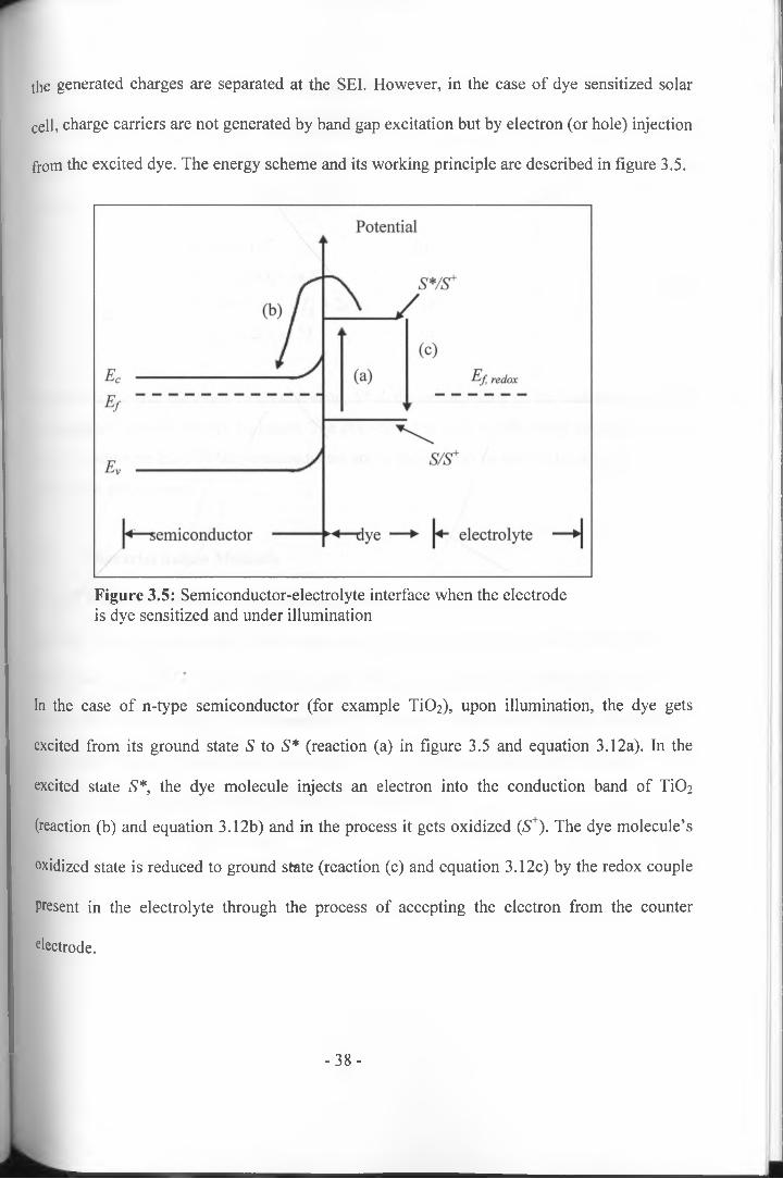
the generated charges are separated at the SEI. However, in the case of dye sensitized solar
cell, charge carriers are not generated by band gap excitation but by electron (or hole) injection
from the excited dye. The energy scheme and its working principle are described in figure 3.5.
Figure 3.5: Semiconductor-electrolyte interface when the electrode is dye sensitized and under illumination
In the case of n-type semiconductor (for example TiOa), upon illumination, the dye gets
excited from its ground state S to S* (reaction (a) in figure 3.5 and equation 3.12a). In the
excited state S*, the dye molecule injects an electron into the conduction band of TiC>2
(reaction (b) and equation 3.12b) and in the process it gets oxidized (S^). The dye molecule’s
oxidized state is reduced to ground state (reaction (c) and equation 3.12c) by the redox couple
Present in the electrolyte through the process of accepting the electron from the counter
electrode.
- 3 8 -

R eaction (b) takes place if the dye is in close contact with the semiconductor surface during
the excited state lifetime and also if the dye lies energetically above the conduction band of the
seniiconductor. The chemical reaction processes discussed above are summarized in equation
(3.12):
s Ugh‘ > s ' (a)
S ' + e - ( T i 0 2) - > S + 0b)
S + + 3 r - > S + i ; + 2 e - (c)
I~ + e - ( C E ) - * 3 r (d)
(3.12)
where S is the dye molecule in ground state, S* is the excited state of the molecule and S+ is
the oxidized state of the dye molecule. The dye should be able to efficiently inject an electron
in the conduction band of the semiconductor and it should also be able to be regenerated by I'
back to its ground state.
3.3 Characterization Methods
3.3.1 X-ray photoelectron spectroscopy (XPS)
In XPS, electrons are emitted from the sample as a response to incoming x-ray photons as
illustrated in figure 3.6. The electrons acquire enough energy from the photons to enable them
escape from the atom and its environment. If the energy of the electron is well defined (hv),
the kinetic energy of the emitted electron (Ex) can be used to determine the electron binding
energy, Eb via the photoelectric effect law (Verma, 2007):
EK = h v - E vB (3.13)
- 3 9 -

Figure 3.6: An illustration showing x-ray photons withenough energy to remove the core electrons of a material,i.e., to lift them energetically above the vacuum level (Verma, 2007).
With the knowledge of the electron binding energy, one can map all the occupied electronic
levels reachable with the photon energy used, from the innermost core orbital to the outermost
valance orbital. From equation (3.13), the intensity of the emitted electrons is plotted as a
function of the binding energy resulting in a spectrum similar to the one presented in figure
3.7. Since the binding energies of core levels are not involved in molecular or solid state
bonding, they are always atom specific and as such these energies can be used to make
elemental compositional analysis of the sample. The core levels however, vary in binding
energy depending on the chemical environment (also known as chemical shift). The chemical
shift may be explained in terms of the changes in electrostatic potential of the core orbital upon
- 4 0 -

chemical changes. On this basis therefore, the chemical shifts provide information on the
oxidation state and chemical environment of the atoms.
Figure 3.7: Typical XPS spectra showing characteristic Ols core level peak in Ti0 2 (Rensmo, et. al., 1999).
The system used in XPS studies consists of an x-ray source of specific wavelength incident on
a sample and a detector that detects the emitted photoelectrons. The electrons are emitted from
the atom in all directions and they undergo inelastic collision inside the chamber. Before being
detected the electrons are focused by an electron lens system and then dispersed in terms of
kinetic energy by a hemispherical electrostatic analyzer.
-41 -

3.3.2 X-ray diffraction (XRD).
X-rays are high energy electromagnetic radiation, having energies ranging from about 200 eV
t0 1 MeV. X-rays are produced in an x-ray tube consisting of two electrodes in a vacuum
ch a m b e r. If an incident electron has sufficient energy to eject an inner-shell electron, the atom
will be left in an excited state with a hole in the electron shell. When the hole is filled from an
outer shell, an x-ray photon with energy equal to the difference in the electron energy levels is
produced. The energy of the x-ray photon is characteristic of the target material and will be
displayed in form of high intensity peaks (known as characteristic peaks) that are used for
diffraction analysis. When these x-rays are focused on a material, they get scattered by the
atoms in specific directions according to Bragg’s law (Suryanarayana and Norton, 1998):
X = 2ndhkl sin 6 (3.14)
where A is the wavelength of the x-rays, dm is the crystal’s inter-planar spacing and 6 is the
angle of incidence.
Equation (3.14) is used in the analysis of the diffraction patterns of sample material and hence
is used for elemental identification and also the kind of crystal orientation. The diffraction
pattern of the sample is obtained by plotting the peak intensity on the y-axis and the measured
diffraction angle (20) on the x-axis. A typical x-ray diffraction pattern is shown in figure 3.8.
fhe diffraction pattern consists of a series of peaks which corresponds to x-rays diffracted
from a specific set of planes in the specimen. The pattern shown in figure 3.8 is the powder
diffraction file (PDF) standard from the reference library for Barium Titanate (Remel, et.
a'-,\999). The positions of peaks depend on the crystal structure (shape and size of the unit
CeH) of the material that enables the determination of structure and lattice parameter of the
- 4 2 -

material. The actual patterns obtained may vary slightly from the standard ones and the main
variation arises from the peak broadening that is mainly caused by the size of the crystal and
the overlapping of peaks.
Figure 3.8: A typical XRD pattern of barium titanet (Remel, et. al., 1999).
Apart from identifying peaks, XRD also gives information about the crystal sizes of the
samples. This is determined from the Scherer’s formula given by (Suryanarayana and Norton,
1998)
n . i ■ 180 ** , , 1CNCrystal size = ----------- . (3.15)* cos yJ(FWHM)2 - S f
where k is the Scherer constant (= 0.8.9), this is the ratio between full width at half maximum
(FWHM) and integral breadth, S, is the instrument broadening (assumed to be = 0), X is the
wavelength of the incident radiation (which is equal to 1.54 A for the instrument used).
- 4 3 -

3 3 3 Current-voltage (I-V) characterization
So lar energy consists of an electromagnetic spectrum of different wavelengths ranging from
u ltravio let (UV), visible and infra red regions. From the theory of blackbody radiation, the
dc /energy density per wavelength, , can be expressed as a function of wavelength (2 ) as
(WiirfeK 2005),
where dQ is a solid angle element, c is the velocity of light in the medium, ks and h are
Boltzmann’s and Planck’s constants, respectively. The maximum density per wavelength is
the earth’s atmosphere. On passing through the atmosphere, the spectrum is partially
through which radiation passes. AM is given by the ratio l/l0 where l0 is the thickness of the
atmosphere, / is the path length through which the radiation passes at an incident angle a
relative to the earth’s surface normal. Therefore l is given by
der(X) _ 2hc0dQ 1
dX ~ dX e% j _ j(3.16)
he _ 0.2497 4 9 6 5 k J ~ kBT
(3.17)
The power density at the sun’s surface is 62 MWm' and it reduces to 1353 WnT just outside
attenuated by the absorption of O2, Ozone, water vapor, CO2 and methane. This attenuation is
described by the ‘Air Mass’ (AM) factor since the absorption increases with the mass of air
l = / 0 / cos or (3.18)
The spectrum outside the atmosphere is AMO and that on the earth’s surface for perpendicular
•ncidence is AMI. The standard spectrum for moderate weather is AM 1.5, which corresponds
- 4 4 -

to a solar incident angle of 48° relative to the surface normal, giving a mean irradiance of 1000
Wm'2-
l-V measurement determines the current-voltage response of the device, i.e., I-V characteristics
;n the dark and under different light intensities. In the dark, the solar cell device is modeled as
an ideal diode where the applied voltage (known as bias voltage) on the device generates
current in the direction opposite to that of light generated current. This current is known as
dark current and is given by (Sze, 1981)
where Is is the saturation current, V is the applied voltage and e is the elementary charge.
Under illumination, the I-V characteristics are of the form:
/ = / „ - / , ( e x p ( < % ) - l )
= Iph " Is[exv[ V/ y 1 “ 1 (3.20)
where Iph is the photo-generated current and VT is the thermal voltage (= ksT/e).
For non-ideal devices, the ideality factor, m is used to describe the dependence of dark current
on voltage, giving the equation (Nelson, 2003),
1 = 1 ph -J eXP mVr - 1 (3.21)
Equation 3.21 can be obtained experimentally by plotting photocurrent as a function of applied
bias resulting in a typical curve known as the current- voltage {I-V) characteristics curve
(Figure 3.9).
- 4 5 -

0P h o t o v o l t a g e (V)
0.1 0.2 0.3 0.4 0.5 0.6 0.7 0.8
Figure 3.9: A typical I-V curve showing variation of current with voltage and corresponding power curve (Nelson, 2010).
From the I-V curve, important parameters namely open circuit photovoltage (V^), short circuit
photocurrent (Isc), fill factor (FF) and overall conversion efficiency can be determined.
3J3.1 Open-circuit voltage (VK)
Foe is measured under the condition when the circuit is open (external load is infinite and zero
Power). In this state, there is no external current flow between the two terminals, i.e. 7= 0 and
Vx . From equation (3.21), Vx can hence be determined by (Nelson, 2003),
-46-

f Kv1 + - L
' mVT — 1 = 0 (3.21a)
1 . _ £ i + l = m V , In
( I >1 pH
h ) [ i s J (3.22b)
From (3.21b), Foc increases logarithmically with the photogenerated current and light intensity.
3 3.3.2 Short-circuit current (Isc)
The short-circuit current (Isc) is measured at the condition when the applied voltage is zero,
i.e., the circuit is shorted, and the load and power are zero. From equation (3.22a),
Isc - I pH (3-23)
Isc increases linearly with light intensity.
3.3.3.3 Fill factor (FF)
The output power from the solar cell is the product of photocurrent and the applied voltage. At
short-circuit and open-circuit the output power is zero, which is the case in which no external
work can be performed. At a certain potential between short-circuit and open circuit, a
maximum output power (Pmax), will appear, (figure 3.9), where the device delivers the highest
power output with the voltage, Vmp and the current Imp
K P = ^ o c - ^ K ln
FF is defined as the ratio
V Ioc scf f =
_^L + lj
(3.24)
(3.25)
- 4 7 -

vvhich describes how the maximum power rectangle fits under the I-V characteristics. A
combination of equations (3.24) and (3.25) gives the approximation for FF as in equation
(3-26).
F
F F =‘x/mVr - m + V “mV,
i / .(3.26)
mVT
Typical FF values for DSC range from 0.6 to 0.8 depending on the device. Generally the FF is
influenced by the series resistance (Rs) arising from the internal resistance and resistive
contacts of the cell, and shunt resistance (Rsh) arising from the leakage of current. Figure 3.10
shows an equivalent circuit for a solar cell showing Rs and Rsh.Rs
Figure 3.10: An equivalent circuit for a solar cell showing the series (Rs) and shunt (Rsh) resistances
3.3.3.4 Solar-to-electric power conversion efficiency (//)
This is a parameter that is associated with the overall performance of the device. This is
defined as the ratio of the maximum power (Pmax) to the power of incident radiation (Pm)- It is
given by
V I V I FF ij = = ---- x 100% ( 3 . 2 7 )
- 4 8 -

0f 100 mWcm'2 at 298 K.
y 3,4 Incident photon to current conversion efficiency (IPCE) characterization
analysis of the efficiency of a solar cell’s conversion of light with a specific wavelength to a
photocurrent. It can be performed under monochromatic light in which the photocurrent is
measured for each wavelength. Generally, the IPCE can be expressed as the product of the
absorption (r/abs), injection (rjinj) and collection efficiencies (t]coii).
Experimentally, it is defined as the ratio of number of light-generated electrons in the external
circuit to the number of incident photons at a certain wavelength, i.e.,
IPCE which stands for incident photon-to-current conversion efficiency and it helps in the
IPCE = Nelectron _ ^ e le c t r o n s / S _ ^ph
N photon yN pho tons / photon /
electron (3.28)
The rate of arrival of incident photons is directly related to the incident power as follows
Pin(Watt) = Pm Joule _ NphotonK s ) S s A
(3.29)
With Equation (3.29), (3.28) can then be written as
(3.30)
he
For dye sensitized solar cells the customary expression is
A(nm)Pm(mWcm )(3.31)
- 4 9 -

j js the short circuit photocurrent density (measured by a source meter), k is the wavelength
0f incident light, (obtained from the lamp that is set at a particular wavelength by the
Ill0nochromator) and Pm is the incident radiation at a particular wavelength (obtained by an
optical power meter and a detector). A plot of equation (3.31) gives a graph of IPCE (%) at
different wavelengths (k). The process of obtaining IPCE can be automated through various
steps using a data acquisition and instrument control software (see appendix II for program) or
m an u ally obtained.
3.4 Charge Transport and Recombination
Charge transport and recombination studies are done by electron transport and lifetime
measurements respectively. Lifetime measurement helps to analyze the recombination process
in the DSC. Both electron transport and lifetime studies can be performed by applying a small
square light modulation under a bias illumination giving a response similar to one in figure
3.11. The response (photocurrent or photovoltage) profile follows the square wave light
modulation (lines with dots in figure 3.11) from which the amplitude (which is A /or AT) and
response time (which is transport time, t,r or recombination time, trec) of the transient, is
calculated. For photovoltage transient, the response time is attributed to the electron lifetime
(which is also recombination time rate trec) of the system. This is highly dependent on the bias
illumination level and therefore on the open circuit voltage.
- 5 0 -

1.01
Time (s)
Figure 3.11: The photocurrent response to a small-amplitude square waveform perturbation. The solid line is the square pulse while the dotted line is the response (Boschloo, et. al., 2006).
Electron transport measurement is performed in order to analyze the conduction of electrons in
the porous semiconductor. The measurement is performed during a modulation of the light
under a bias light condition and while recording the photocurrent response. Normally, the
measurement is performed in short circuit mode. The perturbations are performed with a
frequency resolved method, intensity modulated photocurrent spectroscopy.
I he photocurrent responses for both methods are analyzed to estimate a transport time. Typical
photocurrent transients and the resulting transport time are shown in figure 3.12.
-51 -

0.1
1 U -2P h o t o c u r r e n t (m A cm )
100
Figure 3.12: Typical responses showing transport time plotted as a function of photocurrent. Inset is the photocurrent decay for a single bias intensity (Boschloo, et. al., 2006).
Photocurrent transients (inset of figure 3.12) and their corresponding transport times have
similar profiles like for photovoltage but the difference is their magnitudes. To obtain
information about transport and recombination, the current and voltage responses are fitted to
first order exponential functions as expressed in equations (3.32) and (3.33), respectively (Van
de Lagemaat and Frank, 2001) to give the profile in figure 3.12.
J s c ~ J sc fi + " (3.32)
(3.33)
The constants JSCi0 and VOCfo represent Voc and Jsc without modulations, AJ and AV are the
m°dulation magnitudes, and t,r and trec the time constants for transport and recombination,
-52-

respectively* Normally, only one time constant is seen and this is related to the transport time
r [jfetime. Consider figure 3.13 showing typical photocurrent decay from a single value of
modulation intensity.
Figure 3.13: A sketch of photocurrent decay for one value of modulation intensity.
The time constants of the electron transport times and lifetimes are plotted against the
photocurrent at different bias light intensities on a logarithmic scale giving a straight line for
both transport time and lifetime. The decay follows the model presented in equation (3.32)
with the parameters present indicated on the sketch. Transport time constant (t,r) is
approximated to be the time just at the onset of constant current density and AJ0 being the
difference between the initial transient current (Jsc,max) and the constant current (offset current,
•Ac.o). To obtain a fit to the above transient, equation (3.32) is linearised and invoking initial
l'onditions leads to the normalized current transient equation (3.34),
Inf AJ N
V ^o j(3.34)
- 5 3 -

. 0se ploton a seml logarithmic scale gives a linear plot of the form shown in figure 3.14.
Figure 3.14: Normalized photocurrent decay plotted on logarithmic scale.
From the sketch, information about the kind of transport that takes place in the electrode can
be obtained, i.e., whether the decay has a single exponential or more.
3.4.1 Photovoltage decay
The voltage decay analysis provides information about the electron recombination processes in
DSCs. When the cell is illuminated in open circuit mode for some time then switched to the
dark, the decay follows the profile shown in figure 3.15.
- 5 4 -

Figure 3.15: Voc decay with respect to elapsed time in the dark.
Since no current is extracted, the decrease in Voc can only be attributed to recombination
processes in the cell. Therefore the electron lifetime te in the semiconductor (e.g. Ti02) can be
determined using the following relation (Zaban, et. al., 2003):
= —k j dV,ocdt
(3.35)
where ks is boltzmann’s constant, T is temperature and the rest bear their usual meanings.
3-4.2 Charge extraction
When the cell is illuminated while in open circuit mode, it reaches a point when a steady state
ls arrived, i.e. a point where the rates of photogeneration and back reaction of electrons with
tri-iodide are equal. If the illumination is interrupted at this point, and the electron density
allowed to decay for a given time in the dark before short circuiting the cell, then the current
- 5 5 -

measured will correspond to the remaining charge in the film. This method can offer
inform ation on the tra p states in the solar cell where the charge is given by (Duffy, et. al.,
2000a)
.*/Q * r n - Q ^ ~ JNm (E)dE (3.35)
«/
jf (E) is the density of states function of traps (cm'3 eV'1), Ef is the equilibrium dark Fermi
level of electrons in the oxide, determined by the iy i ' couple and „Ef is the quasi Fermi level
of electrons under illumination. Equation (3.35) also provides a direct link between the total
stored charge density and the photo voltage under conditions where the majority of electrons
are located in trapping states.
3.4.3 Electrochemical potential characterization
When a solar cell is illuminated for a short time while it is in short circuit mode then followed
with switching simultaneously to open circuit and in dark, the voltage rises to a maximum
value after a certain time, tmax then slowly decays to zero. The maximum voltage that is
reached, hereafter referred to as the maximum short-circuit voltage (Vsc■ max), is related to the
charge that is left in the nanostructured semiconductor. The value of Vsc, max gives an indication
of the position of the quasi-Fermi level inside the nanostructured TiC>2 film. Typical results are
shown in figure 3.16.
«**•
-56-

Figure 3.16: A sketch of internal voltage decay (Vsc) at different diode bias illumination (Boschloo, et. al., 2006).
As tmax corresponds to the time required to obtain a uniform distribution of the electrons in the
film (assuming that recombination occurs uniformly in the film), it can be considered as a
transport time (Boschloo, et. al., 2006).
-57-

Chapter Four
Experimental Methods
4 1 Introduction
This chapter describes the relevant experimental details of device preparation, characterization
and analysis used in this work. In the first part, details of glass substrates, TiC^ pastes,
sensitizers, electrolytes and counter electrodes are described, as well as the assembling
procedure of the whole device. The extraction of anthocyanin dye pigment is also discussed, as
well as preparation of ruthenium dye complex. In the second part, setups of spectroscopic
methods such as x-ray photoelectron spectroscopy (XPS) and SEM, current-voltage
characterization, IPCE, electrochemical measurements, photo-transient voltage and current
decay experiments, are explained. All reagents and solvents used in this work were of
analytical grade and were supplied by Sigma Aldrich unless stated otherwise, ruthenium
complex dyes were acquired from Solaronix SA, Switzerland. The F:Sn02 conducting glasses
used as substrates for photo and counter electrodes were TEC 8 from Pilkington Inc, USA
coated with fluorine doped tin oxide (sheet resistance = 8 fl/cm2). The solar cells used to study
current-voltage characteristics for anthocyanin dye pigment had 6.5 pm film thickness and
exposed area of 0.48 cm2 while the ones used to study film thickness related electron transport
had 3.0 pm, 6.0 pm, 12.8 pm, 23.5 pm and 25.3 pm film thicknesses and exposed area of 0.48
cm2.
-58-

2 Sample Preparation
4 2.1 Dye preparation
The anthocyanin dye pigment was extracted from viola odorata (common name sweet violet)
flow er in ethanol/water (at ratio 1:1) at room temperature. The solid residues were filtered out
and the natural dye pigments concentrated by a rotary evaporator at 40 °C. The extract was
then dried over magnesium sulphate to form pellets. The pellets were then centrifuged at a rate
of 1800 rpm for 15 minutes at room temperature then dissolved in 10% acetonitrile, 0.1% TFA
eluent. Ruthenium complex dye was prepared by dissolving 0.0315g of cis-
di(thiocyanato)bis((2,2’-bipyridyl-4,4’- decarboxylate)-ruthenium II (commonly known as
N719) complex in 50 ml 99.5 % ethanol. The resulting dye solution of 0.5 mM concentration
was stirred for 3 hours and kept in a cool dark place ready for dye sensitization.
4.2.2 Dye characterization
Anthocyanin dye pigment was characterized using Metrohm 654 pH meter (Metrohm,
Switzerland) calibrated with buffer 1 (pH 4.5) and buffer 2 (pH 9.0) for dissociation
characteristics. The dye’s pH was increased by addition of 10.0 pi, 0.01M dropwise as the pH
was read off from the pH meter. To obtain the dye’s pH below 2.50, 10.0 pi of concentrated
hydrochloric acid was introduced in the dye as the pH was monitored.
The dye’s absorption characteristics were studied using UV-Vis spectrophotometer at
wavelengths 400 nm to 800 nm. The absorption characteristics were recorded for anthocyanin
tye in solution and also for photoelectrodes sensitized with anthocyanin pigment at different
PH levels. The empty cuvette was used as a reference for studies on dyes in solution while the
- 5 9 -

llflSSfl
cases.
sitized Ti02 photoelectrode was used as reference for the dye sensitized film. In both
the respective spectra recorded were subtracted from the reference spectra.
4 2 3 TiCh paste preparation
The materials for preparation of Ti02 paste were P25 (30 nm by Brunauer-Emmett-Teller
(BET), 80% anatase (d = 21 nm) and 20% rutile (d = 50 nm)) from Degussa AG, Germany,
ethyl cellulose (5 -15 mPas at 5% in Toluene:Ethanol/80:20 at 25°C).
6.0 g of P25 Degussa was mixed with 1.0 ml acetic acid and ground in a mortar for five
minutes. This was followed by addition of 5.0 ml de-ionized water dropwise while grinding in
a mortar for another five minutes. 30.0 ml of ethanol was then added in steps of 5.0 ml with
continuous grinding and finally 100.0 ml of ethanol added. The paste was transferred to a
250.0 ml beaker then stirred for 2 minutes followed by sonication using Branson model 240
Digital Sonicator horn, (Branson Ultrasonics Corp, USA) and stirred again for another 2
minutes. The colloid in ethanol was then mixed with 20.0 g of tarpineol and followed by
further stirring - sonication - stirring process. The same process was repeated after addition of
10% ethyl cellulose (Fluka GmbH, Germany) in ethanol to the colloid and then concentrated in
a rotor vapour and collected in a reagent bottle. The resulting paste of about 21% by weight of
TiC>2 was run through a three-roll miller and collected in a bottle.
4.2.4 Thin film deposition
The Ti02 paste was used to coat films on F:Sn0 2 conducting glass substrate by screen printing
Method. The mesh size was 6x8 mm and one frame had 20 mesh openings that gave a total of
- 6 0 -

90 films at a single coating. To coat subsequent layers, the coated film was heated at a
temperature of 150 °C for five minutes and left to cool to room temperature then another coat
applied until the required number of coatings was achieved. The films were then sintered in air
for one hour at 450 °C and left to cool to room temperature. The film thicknesses were
determ ined by Alpha Step 200 surface profilometer (Tencor Instruments Inc, USA). These
films were either used for XRD, SEM and XPS analysis or assembled into complete solar cells
for I- V, and transport/recombination analysis, after determining the film thickness.
4.2.5 Counter-electrode preparation
Pre-drilled F:Sn02 conducting glass substrates were cut into 1.5 x 1.5 cm sizes and cleaned in
the ultrasonic bath using ethanol, water and acetone for 10 minutes in each following that
order. The cleaned glass substrates were then dried in hot air gun for 30 minutes at a
temperature of 400 °C and cooled to room temperature. 10.0 pl/cm2 of 4.8 mM
hexacholoroplatinic acid (TEPtCh) in ethanol was spread on the conducting side of the glass
substrate and heated again in a hot air gun for 30 minutes at a temperature of 400 °C. The
counter electrodes were then cooled in air before using them.
4.2.6 Electrolyte preparation
The electrolyte used in this study is composed of 0.5 M tetraLutyl ammonium iodide (TBA-I),
0.5 M 4-tert-butyl pyridine (4-TBPy), 0.1 M lithium iodide and 0.1 M iodine dissolved in 3-
methoxypropionitrile (3-MPN), also known as the standard electrolyte. The electrolyte was
P^pared as follows: 0.069 g lithium iodide, 1.108 g TBA-I, 0.369g TBPy and 0.126 g of
'°dine crystals were weighed using a high precision analytical balance and transferred in a
-6 1 -

dark bottle in that order. 5ml of 3-MPN was used to dissolve the mixture to make the required
concentration which was followed by s tir r in g for 3 hours. The electrolyte was then stored at
room temperature and used when needed.
4 2.7 Complete solar cell assembly
TiCh coated films that were used for dye sensitization were cooled to 80 °C after sintering and
then immersed in the dye (anthocyanin or ruthenium complex) that was at room temperature,
for 12 hours. The samples were subsequently rinsed in acetonitrile, dried briefly on a hot plate
and then thermally fused together with 25 pm thick thermoplastic surlyn frame (Dupont Inc,
USA) on a hot plate. The electrolyte was introduced though the holes on the counter electrode
by applying a few drops using a micropipette until the electrolyte was completely filled inside
the cell. The cell was then placed in a vacuum sealed bell jar followed by air extraction leaving
the electrolyte only in the cell. The cell was removed from the bell jar and the excess
electrolyte wiped away and further sealed with surlyn and microscope cover glass. Silver
contact paint was finally applied on the edges of the working and counter electrodes to offer
less resistance contact for the solar cells.
4.3 Thin Film Characterization
4.3.1 Scanning electron microscopy (SEM)
SEM was used to study the morphological characteristics of the films. This was done using*»*■
Carl Zeiss™ LEO 1550 scanning electron microscope with Gemini column at 20kV electron
source. The SEM micrographs were taken using a CCD (charged coupled device) camera
- 6 2 -

interfaced to a computer. Different micrographs were taken at different magnifications that
^ged from XI 0,000 to X200,000.
4 3 2 X-Ray Diffraction (XRD)
X-ray diffraction was obtained by means of Siemens D5000 Diffractometer (Bruker AXS
GmbH, Germany) with 0-20 parallel beam geometry. The range was from 10° to 80° with
detector type of scan at a scan speed of 0.6°/min and step size of 0.01°. The stage was set to
rotate at 15 rotations per minute. XRD peak references were obtained from International
Centre for Diffraction Data, USA.
4.3.3 X-Ray Photoelectron spectroscopy (XPS)
XPS spectra were recorded using Quantum 2000 scanning ESCA p-probe (Physical
Electronics Inc., USA) with A1 Ka x-ray source with photon energy of 1486.6 eV. The
equipment uses a rotating anode high power x-ray source and a quartz crystal monochromator
delivering A1 Ka radiation. The instrument has a 300 mm radius hemispherical electron energy
analyzer and a swift sample transport system from air to ultra high vacuum chamber.
44. Solar Cell Characterization
4.4.1 1-V characterization
Current-voltage (I-V) characteristics were obtained using a set up (Figure 4.1) consisting of
Newport solar simulator model 91160 (Oriel Instruments, USA) that was set to give an
"radiation of 100 mW/cm2 (equivalent of one sun at AM 1.5) at the surface of the solar cells.
AH the solar cells characterized in this work had an active area of 0.48 cm2. A dark frame was
- 6 3 -

placed on the solar cell sample to ensure that only the solar cell’s active area was illuminated.
The current-voltage characteristics under these conditions were obtained by applying an
external potential bias to the cell and measuring the generated current with a Keithley 2400
digital source meter (Keithley, USA).
Figure 4.1: Block diagram of the current-voltage characterization set up.
The solar cell’s cathode (working electrode) and anode (counter electrode) were connected to
the negative and positive terminals of the Keithley 2400 source meter respectively, which was
connected to the computer via GPIB interface. The bias was from short circuit to open circuit
and was obtained automatically using LabVIEWIM software from National Instruments Inc,
USA (see appendix I for details on automation in LabVIEW). From the data, an I-V curve was***■
Plotted in real time and the parameters Voc, Jsc, FF, Pmax and r\ were calculated and displayed
automatically and saved as an excel file. I-V characteristics for anthocyanin dye sensitized
^lar cells were obtained for films sensitized with the dye pigment at pH 1.80, 2.00, 5.17 and
-64-

g 34 and all were 6.5 ± 0.5 pm film thickness. I-V characteristics for anthocyanin sensitized
solar cells and ruthenium N719 sensitized solar cells were compared using cells of film
thickness 3.0 pm and 0.48cm exposed area. For thickness dependent I-V characteristics, I-V
waS recorded for solar cells at varying film thicknesses of 3.0 pm, 6.0 pm, 12.8 pm, 23.5 pm
and 25-3 pm film thicknesses and sensitized with ruthenium N719 dye.
4.4.2 Photoelectrochemical characterization
Cyclic voltametry was carried out on the anthocyanin dye using a three-electrode cell setup
with the sweep generated by Autolab PGSTAT12 potentiostat (Echochemie BY, Netherlands).
Figure 4.2: Set up for cyclic voltametry (CV) studies. RE is reference electrode, WE is the working electrode and CE is the counter electrode.
- 6 5 -

The electrodes were silver/silver chloride reference electrode, glassy carbon working electrode
and platinum counter electrode. The base solvent was acetonitrile with lithium iodide salt to
provide the ions. Before the study was done on the dye, the potentiostat was calibrated by
using the dummy cell used in place of the electrochemical cell. The dummy cell has three
electrodes (WE, RE and CE) which were connected to the potentiostat and a test run taken.
Thereafter the electrodes to be used in the experiment were rinsed in de-ionized water and a
calibration run done using ferrocene. Ferrocene was dissolved in acetonitrile and used as the
analyte with the three electrodes immersed in the single compartment electrochemical cell in
the positions indicated in figure 4.2. The resulting scan was compared with the standard scan.
Anthocyanin dye pigment was then mixed with 0.1 M Lil as the supporting electrolyte in
acetonitrile as the solvent. The mixture was transferred into a single compartment
electrochemical cell. The three electrodes (RE, WE and CE) were then immersed in the cell
with their tips close to one another. The electrodes were connected to the potentiostat as shown
in figure 4.2. The potentiostat was connected to the computer via RS 232 serial interface bus
which was used to remotely control the potentiostat and to analyze and display the resulting
scan. The potentiostat was set to sweep from 0 V to +1.6 V then reversed to -1.5 V and back to
0 V. The scan rate was 200 mV/s and the voltamogram plotted by the electrochemical analyzer
software. The scans were taken in various conditions beginning with steady state, purging with
nitrogen and then purging with oxygen.
- 6 6 -

4 4 3 Incident Photon-to-Current conversion Efficiency {IPCE).
ipCE was measured using a set up consisting of a white light source, ARC SpectraPro 150
monochromator (Princeton Instruments), Oriel OPM 70310 optical power meter (Oriel
Instruments) and collimators (schematic set up shown in figure 4.3).
Figure 4.3: Schematic set up for IPCE characterization.
The monochromator, optical power meter and the source meter were connected to the
computer and controlled automatically by LabVIEW program (see appendix II for details of
the development). Before an IPCE was run, the monochromator power was calibrated using a
photodiode in place of the solar cell. The photodiode was illuminated by a collimated light*»+•
from the monochromator and the incident power measured by the optical power meter
connected to the photodiode. This was recorded for wavelengths between 300 nm and 800 nm
at steps of 20 nm. The recorded power was used as power of incident radiation (Pm) during the
calculation of IPCE. The photodiode was then replaced with the solar cell and the terminals
- 6 7 -

0nnected to the Keithley 2400 source meter, which recorded the current generated at each
wavelength. The monochromator was set to scan the wavelength from 300 nm to 800nm in
steps of 20 nm. The measured current and incident power were used to calculate the IPCE at
each wavelength and plotted on a graph.
4 5 Electron Transport and Lifetime Measurements
Electron transport and lifetime measurements were performed using a set up (block diagram in
figure 4.4) consisting of Stanford Research Systems lock-in amplifier model SR 570 (Stanford
Research Systems, USA), HP 33120 function generator, and BNC 2110 data acquisition board
(National instruments Inc, USA). Instrument control and data acquisition was performed
automatically by LabVIEWIM (National Instruments Inc, USA) application via GPIB interface
protocol.
Figure 4.4: Block diagram of the transport and lifetime studies set up.
- 6 8 -

fhe light source was from a square pulsed laser diode (LabLaser, Coherent LabLaser, USA)
vith/Uiox 635 nm biased with voltages 3.0, 2.5, 2.2, 2.0, 1.9 and 1.85 V giving light intensities
0f 15.5, 9.01, 5.07, 2.44, 1.15 and 0.51 mWcm'2, respectively. Switching from potentiostatic
(t0 measure in short circuit) and galvanostatic (in open circuit) was achieved by use of a solid
state switch.
A small square wave modulation (<10% intensity, 0 . 1 - 2 Hz) was added to the base light
intensity. The solar cell response (I or V transients) was fitted to exponential rise or decay
function using a nonlinear least-squares fit. Traces were averaged 10 times for transport and 2
times for recombination studies. The set up described above was used to perform photocurrent
transient spectroscopy (for electron transport studies), photovoltage transient spectroscopy (for
electron lifetime studies) photovoltage decay studies, charge extraction experiments and
electrochemical potential analysis for complete solar cells at 3.0 pm, 6.0 pm, 12.8 pm, 23.5
and 25.3 pm film thickness.
4.5.1 Photocurrent and voltage transient
In photocurrent transient set up, the cell was kept in short circuit mode by the solid state
switch and the LED was manually biased in the steps 3.0, 2.5, 2.2, 2.0, 1.9 and 1.85 V, with
transients recorded at each bias. From the transients and the fit, the time constants (which are
the transport times) were calculated for each value of intensity and recorded against the*»*■
corresponding current constant.
- 6 9 -

photo voltage transient routine was similar to photocurrent’s but the cell was set to open circuit
for measurement of photovoltage decay. The time constants were calculated for each value of
intensity and recorded against the corresponding photovoltage value. The illumination was
done for substrate-electrode (SE), also known as backside, and electrolyte-electrode (EE) also
l^own as front side illumination, modes and data recorded for each.
4.5.2 Photovoltage decay measurement
In this set up, the cell was illuminated under open circuit mode for some time then the laser
was switched off. The voltage decay was monitored and recorded over time and used to
calculate the electron lifetime from the relation earlier given in section 3.4.1, i.e.,
r„ = —k j dV,oc
dt(5.1)
for film thicknesses 3.0, 6.0, 12.8, 23.5 and 25.3 pm.
4.5.3 Charge extraction
In the charge extraction experiment, the solar cell was illuminated with a pulsed laser light in
short circuit mode for 2 seconds then switched to dark. The current decay transient that
followed was measured and integrated over a period of 10 s. The integration gave the quantity
of charge that remained in the solar cell and was studied against the varying intensities and
film thicknesses.
4.5.4 Electrochemical potential analysis
h this study, the solar cell was illuminated under short-circuit conditions for 2 seconds then
fite laser was switched off and the cell switched to open circuit, simultaneously. The voltage
- 7 0 -

hange was t^en recorded over time. This was done at different laser biasing giving the
incident illumination intensities 15.5, 9.01, 5.07, 2.44, 1.15 and 0.51 mWcnf2 for each film
sickness. The maximum voltage (VSCf max) and the time (tmax) at which it was attained were
recorded.

Chapter Five
Results and Discussion
e 1 Introduction
In this chapter, structural (SEM, XRD and XPS) characteristics of Ti02 photoelectrodes coated
by screen printing method are discussed and analyzed. This is followed by analyzing the
results from the dye pigment’s absorption spectroscopy; IPCE and IV characteristics of the
solar cell sensitized with anthocyanin dye compared with ruthenium complex dye. The chapter
ends with the analysis of charge transport properties in these films of varying film thicknesses
employing various routines like photovoltage decay, time resolved photocurrent spectroscopy
and charge extraction among others.
5.2 Structural Characterization
SEM micrographs for films produced by screen printing method and doctor blade technique
are presented in figure 5.1.
Figure 5.1: SEM micrograph for (a) screen printed TiC>2 film with P25 as theParting material (b) coated by doctor blade with titanium tetrachloride as the starting material.
- 72 -

micrographs show that screen printing method produced films with nanometer sized
articles, varying in sizes between 15 nm and 40 nm (Figure 5.1a). This is in agreement with
the composition of P25 where 70 % is anatase (smaller particles) and 30 % is rutile (larger
particles). Comparing with the micrograph of TiC>2 film made of colloids prepared from
titanium isopropoxide synthesis coated by doctor blade technique (Figure 5.1b), the P25 film
(Figure 5.1a) appeared more homogeneously dispersed. The particle sizes for TiC>2 colloids
prepared from titanium isopropoxide (Figure 5.1b) appeared to be of smaller size (average
particle size for these films was between 10 and 20nm) as compared to the screen printed
films. The difference may be attributed to the synthesis method employed in preparation of the
colloidal paste from titanium isopropoxide especially at the autoclave stage. The particle size
has been studied elsewhere and found to depend on the autoclave temperature (Barbe, et. al.,
1997; Ito, et. al., 2007) for the colloidal paste. The dependence of particle size to autoclave
temperature was explained by Barbe’s group to be due to sedimentation of TiC>2 particles
during the hydrothermal synthesis. Autoclaving temperature helps in the growth of the primary
particles by dissolution-re-precipitation mechanism that occurs under the hydrothermal
conditions.
X-ray diffraction (XRD) scans (Figure 5.2) showed that the films produced were crystalline in
nature (an observation of strong distinct peaks with different crystal orientations). Strong TiC>2
anatase peaks with crystal orientation directions (101) were observed for both films. The other•a-
Peaks (200), (211), (112) and (105) are all for anatase phase. The scans for the films from
screen-printed P25 and doctor blade coated colloidal paste were identical implying that the
screen-printing method produced TiC>2 paste with similar characteristics as the colloidal one
- 73 -

ejccept for the variation in particle sizes. The colloidal film had slightly broader peaks (as
determined by Scherrer’s formula, implying smaller particle size), corroborating the SEM
r e su lts .
Figure 5.2: XRD surface scans for TiC>2 films made from (a) P25 by screen printing and (b) colloidal TiC>2 by doctor blade techniques.
Analysis of the peaks of XRD scans for the screen-printed film using Scherrer's formula
showed that anatase particles had particle sizes ranging from 13 nm to 25 nm when calculated
at a diffraction angle of 25 - 53 degrees (Table 5.1). This is close to the results obtained from
SEM micrographs. The particle size could not be approximated for peaks at 53.98° and 55.17°
because the peaks were not distinctive enough, i.e., the peaks were too broad hence could not
8]ve a good approximation.
-74-

Table 5.1: Table showing peak list and particle size for Ti02 film made from P25
Peak Pos. (2Theta)
h k l Type FWHM(2Th.)
d-spacing(A)
Particle size («m)
25.2500 1 0 1 anatase 0.6047 3.52720 13.537.8742 1 1 2 anatase 0.3064 2.37555 27.447.9700 2 0 0 anatase 0.5791 1.89654 15.0153.9800 105 anatase 0.0010 1.69872 -
55.1700 2 1 1 anatase 0.0010 1.66486 -
62.8600 2 0 4 anatase 0.3512 1.47843 25.38
5.3 X-Ray Photoelectron Spectroscopy (XPS)
Results for XPS studies on Ti02 films with P25 as the starting material, are presented in figure
5.3, showing the complete XPS spectrum.
Figure 5.3: XPS spectraior screen printed Ti02 film showing Ti 2p and O 1 s peaks for titanium and oxygen species respectively.
In the spectrum, strong O Is peak for oxygen and Ti 2p for titanium were observed at binding
energies (BE) 530 eV for O Is and 460 eV respectively. Closer inspection of the spectrum
showed that Ti 2p level was split into closely spaced photoemission doublet. This was seen
-75-

clearly when the spectrum in the region of Ti 2p was expanded giving rise to two distinct
peaks at 461.5 eV and 467.0 eV of binding energy (BE) (Figure 5.4a). Similar expansion for O
Is showed only one distinct peak at 529.9 eV as shown in figure 5.4b. The two peaks for Ti 2p
photoemission had intensity ratio of 1:3 for 467 eV and 461.5 eV, respectively.
Figure 5.4: XPS spectra for TiC>2 showing (a) Ti 2p and (b) O Is peaks.
Photoemission splitting has been observed before by other groups (Ingo, et. al., 1993; Reddy,
et. al., 2001; Sandell, et. al., 2002) and is attributed to spin-orbit coupling effects in the final
states of the compounds investigated. The same case may be for Ti where the core electronic
configuration in initial state changes when photo-ionization in 2p state leads to a removal of an
electron changing the configuration in the final state. From the intensity ratio of 1:3 the
degeneracies of the final states were deduced to be Vi and 3/2 giving rise to states Ti 2pi/2 and
^ 2p3/2, respectively. The spin-orbit splitting was not observed at s-level for oxygen. The
aPpearance of only one distinct peak for O Is peak at 529.9 eV (Figure 5.4b) implied that Ti
Was completely oxidized in this film with only one oxygen species. Another case that was
-76-

noted was the peak shift in Ti 2p states for titanium (Figure 5.4a). Previous studies by other
groups (Ingo, et. al., 1993; Reddy, et. al., 2001; Sandell, et. al., 2002; Sandell et al., 2003) on
titanium have shown that it exhibits large chemical shifts between different oxidation states of
^ metal. Standard XPS studies on pure titanium has shown the 2pi/2 and 2p3/2 states to be at
455.0 eV and 461.0 eV. In the present study, the two states were observed at binding energy
(BE) 461.5 eV and 467.0 eV with the two spin orbit components exhibiting a constant
chemical shift of about 6 eV. This may be explained as follows: The position of orbitals in an
atom is sensitive to the chemical environment of the atom. The chemical environments for
pure titanium and when bonded with oxygen are different. When titanium bonds with oxygen,
a charge is withdrawn leading to Ti reducing to Ti4+. This consequently leads to an increase in
the binding energy which leads to 2p orbital relaxing to a higher binding energy (i.e. from
455.0 eV to 461.5 eV and 461.0 to 467.0 for 2pi/2 and 2p3/2, respectively). The appearance of a
constant relaxation magnitude of 6 eV implies that the process is an initial state effect, a case
that is observed in core levels of solids.
5.4 Dye Characterization
Figure 5.5 shows the titration curve for anthocyanin pigment for determining the dissociation
point of the dye molecule. Between pH 2.10 and pH 3.50, the dye solution retained its violet
color but as the pH increased towards pH 4.00, the dye pigment turned colorless. The colorless
appearance lasted in the range between pH 4.06 and pH 4.70 then it gradually turned green as
PH reached 5.70. The solution retained the green color from pH 5.70 to 9.80 then gradually
turned yellowish orange. From the plot of the titration curve (Figure 5.5), violet dye had a
Point of inflexion at pH 4.50 (the same pH value the solution turned from colorless to green).
-77-

Figure 5.5: Titration curve for violet dye using 0.01M NaOH.
Results for absorption characteristics are given in figure 5.6 showing the absorption
characteristics for the dye pigment before and after adsorption on the Ti02 photoelectrode.
■ i X T T « 1 1 i 1 J * l " l I I u * r i
400 450 500 550 600 650 700 750 800W avelength (nm )
Figure 5.6: Absorption spectra for anthocyanin dye pigment (a) before and (b) after being adsorbed on Ti02 photoelectrode.
From the figure, before sensitization, an absorption maximum was observed at 550nm (curve
a) but upon sensitization, there was reduction in absorption intensity which broadened towards
-78-

the longer wavelength (curve b). The minimum observed at 450 nm represents the solution’s
baseline while the maximum observed at 550 nm for plot (a) is consistent with that reported
for delphinidin molecule, the principal anthocyanin compound found in hibiscus sabdarrifa
(polo, et. al., 2006). The difference in the absorption intensity and broadening between the dye
extract in solution and the one adsorbed on TiC>2 could be due to the effect of binding of
anthocyanin molecule in the pigment to the oxide surface (as suggested in figure 5.7) and to
the kind of charge transfer transitions.
Figure 5.7: Schematic representation of anthocyanin attachment (a) by alcoholic condensation and (b) by chelating effect on the TiC>2 surface (Polo, et. al., 2006).
Chemisorption of anthocyanins on TiC>2 has been reported by Hao, et. al., (2006) to be as a
result of alcoholic bound protons which condense with the hydroxyl groups present at the
surface of nanostructured TiC>2 film (figure 5.7a). There also exists the binding of these
molecules on TiC>2 by the chelating effect to the Ti4+ ions, (figure 5.7b) (Garcia, et. al., 2003;
Tennakone, et. al., 1997). This attachment to the TiC>2 surface stabilizes the excited state, thus
shifting the absorption maximum towards the lower energy of the spectrum. Wongcharee, et.
aL, (2007) studied the absorption characteristics on blue pea extract and did not observe any
shift in the absorption maximum. The absence of the shift could imply that there was no
-79-

effective adsorption which was attributed to the kind of structure in blue pea. In their study,
Wongcharee, et. al., (2007) observed that the blue pea had strong presence of tematuin
molecule that is known to have long OH groups. These long OH groups may prevent
anthocyanin from forming a bond with the oxide surface and also from arraying to the Ti0 2
film effectively. In the present study therefore, the shift implies that there is no such hindrance
to the bonding of the OH group with the oxide surface. The shift is also attributed to the
changing of the anthocyanin molecule from the more stable flavilium state to the unstable
quinoidal state upon chelation. These two states are known (Cherapy, et. al., 1997) to exist at
two different pH levels with flavilium being acidic while quinoidal form being basic. In order
to effectively link this observation to the shifting in the anthocyanin states, absorbance
characteristics were studied on the dyes in solution at different pH levels, whose results are
shown in figure 5.8.
*■* W avelength (nm )
Figure 5.8: Absorption spectra for anthocyanin dye in solution at (a) pH 2.00 (b) pH 5.17 (c) pH .07 and (d) pH 8.34.
-80-

jt is observed that the peak that appeared at pH 2.00 disappeared as the pH increased beyond
pH 2.00, being replaced with low absorption intensity and broadening (figures (b), (c) and (d)).
The appearance of a kink at 630 nm on all plots is the effect of detector change over. The
broadening towards the longer wavelength is quite similar to the spectrum for dye-sensitized
photoelectrode (plot b in figure 5.6). Comparing observations in figures 5.6 and 5.8, it may
also be confirmed that upon sensitization, the anthocyanin molecule shifts from the flavilium
to quinoid state which are acidic and basic, respectively. The quinoid states are quite unstable,
a feature that exhibits very weak absorption maxima when the dye is attached on TiC>2. A n
attempt to lower the pH of the dye sensitized film (by fuming HC1 over it) showed the re
appearance of the absorption maximum, almost matching the one for the un-sensitized dye
molecule (Figure 5.9).
Wavelength (nm)Figure 5.9: Absorption spectra for anthocyanin dye pigment (a) before and (b) after sensitization with TiC>2 photoelectrode and fumed with HC1.
- 81 -

rt is further noted that the absorption maximum increases and shifts slightly to the red (plot
(b)) which shows that there is the evidence of chelation between the dye molecule and the Ti4+.
As earlier mentioned, band shifts could be attributed to the molecular transitions that take
place when the dye molecule chelates with Ti02. Anthocyanin pigments exhibit n - n* orbital
transition which is attributed to the 552 nm peak (curve b, figure 5.9). Wang, et. al., (2007) in
their study of sensitization using coumarin dye observed that the introduction of one more
carbon-nitrogen (CN) ligand group into the molecular frame of coumarin decreased the gap
between the highest occupied molecular orbital (HOMO) and lowest unoccupied molecular
orbital (LUMO), thus extending the maximum absorption from 511 to 552 nm. In the present
study, the shift upon sensitization may be similarly attributed to the 7i - 7i* orbital transition
within the dye molecule upon sensitization, also the lowering of the gap between HOMO and
LUMO.
5.5 Solar Cells Characterization
(a) I- V and IPCE characteristics
The current - voltage characteristics for the solar cells sensitized with anthocyanin pigment at
different pH are presented in figure 5.10, compared with Ruthenium N719 sensitized solar cell.
The illumination was incident on the sample from the counter electrode side (known as SE or
backside mode). The characteristics for anthocyanin sensitized cells were seen to depend
strongly on the pH levels of the dye (and hence the absorption characteristics) of the dye
sensitized photoelectrode. The sample with the dye at pH 2.00 had the highest photocurrent
density (and also highest overall efficiency) while the one at pH 1.8 recorded the lowest
efficiency (see summary in Table 5.2).
- 8 2 -

Photovoltage (V)0 0.1 0.2 0.3 0.4 0.5 0.6 0.7 0.8
Figure 5.10: I-V curves for anthocyanin sensitized solar cells at different pH levels compared with Ru N719 sensitized solar cell.
Table 5.2: Summary of IV characteristics for anthocyanin sensitized solar cells at different pH levels
pH Vac(V)
•Isc(mAcm'2)
FF >/(%)
1.80 0.44 0.17 0.66 0.052.00 0.49 3.17 0.66 1.045.17 0.50 0.63 0.65 0.208.34 0.51 0.3 0.57 0.08
The low efficiency observed for anthocyanin sensitized cells at pH 5.17 and above may be
attributed to the fact that an increase in pH hydrated the anthocyanin molecule to quinoid state
which is unstable compared to the lower pH flavilium state. In this scheme, the increase in pH
(more OH groups introduced in the dye) leads to the prevention of anthocyanin molecule from
inning bonds with the oxide surface and also from arraying to the Ti02 film effectively. This
111 turn affects the efficient charge transfer from the excited state of the dye molecule to the
induction band of Ti02. On the other hand it is observed that efficiency dropped
-83-

tremendously when pH was lowered from 2.00 to 1.81, the drop could be due to cell
deterioration by acid leaching. Low efficiency may also be attributed to energy loss via
quenching of the excited dye molecules with each other, instead of being injected into the TiC>2
conduction band.
IPCE results for solar cells sensitized with anthocyanin dye pigment at different pH and
ruthenium N719 are presented in figure 5.11.
Figure 5.11: IPCE for solar cells sensitized with (a) ruthenium N719 and anthocyanin pigment at (b) pH 2.00 (c) pH 8.34 and (d) pH 5.17.
Solar cells sensitized with anthocyanin pigment recorded low IPCE in the visible spectrum
compared to the one sensitized with ruthenium N719. The IP C E ^ of about 4% was observed
at 560 nm for the anthocyanin sensitized cell at pH 2.00 (curve (b), figure 5.11), which
lowered as the spectrum extended towards the infrared. This was the highest IPCEmax observed
ln all the anthocyanin sensitized solar cells characterized. Further observation was that
-84-
ipCEmax reduced and red-shifted as the pH increased from acidic to basic (curves c and d,
figure 5.11). This observation is consistent with absorbance characteristics (figure 5.8) whose
maximum also shifted from shorter wavelengths towards the red as the pH changed from
acidic to basic. Since IPCE consists of injection, transport and collection efficiencies, the low
IPCE reported here could have the contributions from all the three processes but the injection
efficiency could have the most effect. Low injection efficiencies could be due to improper
matching of the dye’s HOMO level (optimal levels are -3.5 to -3.8 eV on vacuum scale) (De
Angelis, et. al., 2008) with the semiconductor’s conduction band (typical levels -4.0 - -4.5 eV
on vacuum scale for Ti02) (Gratzel, 2003; De Angelis, et. al., 2008). The kind of adsorption of
the dye molecule on the Ti02 may contribute to the low IPCE values recorded here. As earlier
discussed in section 5.4, anthocyanin molecules chelate with Ti4+ centres and consequently
shift from the more stable flavilium state to the unstable quinoidal state upon chelation. These
two states exist in acid and basic forms, respectively. The optimal pH of 2.00 shows that at
that pH, there are sufficient OH groups that offer adequate chelation in acidic medium leading
to an improvement in charge injection efficiency from the dye molecule to the Ti02. Whereas
at higher pH (in basic or quinoid form), the excess OH groups present lead to prevention of
anthocyanin molecule from forming bonds with the oxide surface and also from arraying to the
Ti02 film effectively hence lowering the charge injection efficiency.
The characteristics for anthocyanin sensitized film at pH 2.00 that exhibited the best
Performance are compared with ruthenium N719 sensitized cell in table 5.3 in summary form,
from the summary, it can be seen that values for the fill factor for both cells are very close,
-85-

^plying that electrical losses due to series and shunt resistances were very minimal in both
cells-
Table 5.3: A comparison of IV and 1PCE characteristics between anthocyanin sensitized solar cell at pH 2.00 and ruthenium N719 sensitized solar cell
Parameters Anthocyaninsensitized
Ruthenium N719 Sensitized
Voc (V) 0.49 0.83Jsc (mA/cm ) 3.17 6.16FF(%) 66 65« (%) 1.04 3.29IPCEmax, x (nm) 560 540lPCEmax (%) 4 25.5
Other parameters like Voc, Jsc and overall efficiency for anthocyanin sensitized solar cell were
in general half the parameters for ruthenium N719 sensitized solar cell. However, there was a
large difference in the IPCEmax with anthocyanin sensitized solar cell recording a maximum of
4% compared to above 26% for ruthenium N719. The difference in IPCE maximum could be
attributed to the kind of charge transfer transitions that take place between the dye molecule
and the semiconductor where ruthenium sensitizer performs the metal to ligand charge transfer
(MLCT) while anthocyanin performs the ligand to ligand transfer. MLCT transfers are more
efficient than the ligand-ligand transfers and their time constants have been measured and
found to be in orders of picosecond (Gratzel, 2005).
(b) Photoelectrochemical characterization
The results of cyclic voltametry on anthocyanin dye pigment are shown in figure 5.12. The
scans show a deviation from a pure Nemstian profile for a reversible system. Scan (a) was
-86-

jgcorded after stirring the solution and letting it return to equilibrium. This was because a test
^ taken showed that the solution had very slow diffusion hence the need to stir.
10
5
035-5
-10
-15
-2010
5
^ 0<5 -5
-10
-15
-2010
5~ 0 <5-5—-10-15-20
Figure 5.12: Cyclic voltamograms on anthocyanin dye pigment in different environments where (a) the solution is stirred, (b) N2 purged and (c) Ar bubbled.
- 87 -
the potential sweep increased from 0 V at the working electrode, the counter electrode
jj0wed a slow current response which increased exponentially to a maximum as the potential
svveep reached +1.6V. On reversing the sweep towards 0 V, the current response decreased
again exponentially but not retracing the path for potential rise. During this process when the
applied positive potential sweep is run, the concentration of the iodide species decrease at the
working electrode surface which leads to a higher concentration gradient between the two
electrodes leading to a more flux to the surface which leads to the exponential rise in current
observed. As the potential is reversed from the switching point (+1.6 V) towards OV, the
surface concentration begins to rise hence decreasing current. The behaviuor described above
is observed in all the three scans in figure 5.12. The half oxidation and half reduction
discussed so far (from 0 V to +1.6 V and back to 0 V) shows that the reaction does not
undergo any oxidation or reduction (since no peak is observed between 0 V and the switching
potential in both directions).
When the reverse sc#n is swept past 0 V towards -1.5 V an observation of a sudden rise of
anodic current between -0.5 V and -1.0 V suggesting a reduction process of the anthocyanin
pigment. However, on purging, the peak disappeared (scans (b) and (c)). This may indicate
that the peak observed before purging is for impurities present in the analyte and not due to
oxidation process of the dye. Purging process removed any impurities that were present in the
analyte (oxygen included). The absence of the peak implies that dye pigment does not undergo
reduction-oxidation and hence it depends on the electrolyte’s redox species for regeneration
v'a process (5.2c) in the following reaction steps:

s Ugh,->S' (5.2a)S ’ +e-(Ti02) - * S + (5.2b)S + + 3 / ' -> S + I~ + 2e- (5.2c)
1; + e-(C E )-*3I- (5.2d)
That is, the dye molecule is reduced to ground state by accepting an electron from 3T which
itself gets oxidized to r 3 (reactions 5.2c and d).
5,6. Effect of Film Thickness on Electron Transport
The results in this section are for TiC>2 films sensitized with ruthenium N719 dye complex and
studied at film thickness 3.0 pm, 6.0 pm, 12.8 pm, 23.5 pm and 25.3 pm.
5.6.1 I-V characteristics versus film thickness
Figure 5.13 shows I-V characteristics of the solar cells at varying film thicknesses. It is
observed that open circuit photovoltage decreases with increase in film thickness. The film
with lowest thickness (3.0 pm) gave the highest Voc of 0.855 V while the thickest (25.3 pm)
had 0.751 V (Table 5.4). The corresponding short circuit current densities for these films were
3.24 mA/cm2 and 7.57 mA/cm2 yielding FF of 0.699 and 0.643, respectively.
-89-

rP h o to v o l ta g e (V )
0 0 . 2 0 . 4 0 . 6 0 . 8
Figure 5.13: /- V characteristics of sealed solar cells from screen printed TiC>2 films of varying thicknesses.
Table 5.4: I-V characteristics for solar cells sensitized with ruthenium N719 at varying film thickness
SampleThickness (pm)
Voc(V)
■/sc
(mA/cm2)FF Efficiency
(%)3.0 ±0.2 0.835 3.24 0.699 1.896.0± 0.2 0.825 6.16 0.649 3.2912.8± 0.2 0.778 9.75 0.625 4.7423.5± 0.2 0.759 8.39 0.653 4.1625.3± 0.2 0.751 7.57 0.643 3.66
As earlier discussed in section 3.2.1, the of an electrochemical cell is determined by the
difference between the Fermi level t)f the semiconductor and the redox potential (Efredox) of the
redox electrolyte. Therefore the high Voc observed for 3.0 pm thick film may imply that the
diflerence in the Fermi level is large for this film as compared to the 25.3 pm. Since the
electrolyte used in this study was same all through (implying that the redox potential was same
-90-

in all the cells), it leads to a suggestion that film thickness has an effect on the quasi Fermi
level („£/) of the semiconductor. Since „£/ is directly related to the density of conduction band
electrons (nc), it leads to a suggestion that in thinner films, the electron density in the
conduction band is high due to high injection levels. This is because the electron injection
point in the thinner film (e.g., 3.0 pm) is quite close to the charge collection site (and since the
cell is in open circuit), leads to a quick build-up of charges. This raises the „£/(but maintaining
a constant Efred0X) which effectively increases Voc. For thicker films however, it takes
sometime for the charge to build up leading to a lower Voc compared to the 3.0 pm. This is
because the charge injection site is further away from the collection site and hence the
diffusion of charges in the mesoporous structure leads to a slow build-up of potential. This
effectively leads to a lower value of Voc measured in the cell.
Short circuit photocurrent density exhibited a different relationship with the film thickness
(figure 5.14). It was observed that short circuit photocurrent density increased with film
thickness to an optimal value of thickness of 12.8 pm then it reduced again as with increase in
film thickness. The variation of photocurrent density with film thickness may imply that
electron recombination with the redox electrolyte plays a role in cells at short circuit mode, as
herein discussed in the next paragraph.
-91-

Figure 5.14: Relationship between film thickness (d) and short circuit photocurrent density (Jsc).
The observation depicted in fig 5.14 may imply that in the 3.0 pm thick film, both electron
recombination via redox electrolyte and collection at the TCO are high in the film leading to
very low Jsc. However, as the film thickness increases and more electrons are generated, more
are collected and less recombine. A balance between recombination and collection is attained
at film thickness of around 12 - 15 pm (stationary point on the plot in figure 5.14) then beyond
that there is a decrease in Jsc with further increase in film thickness. This may mean that at film
thicknesses beyond 12.8 pm, the cell experiences more recombination via the redox electrolyte
3s compared to charge collection at the TiCVTCO interface. This leads to less charge
collection at the interface leading to low Jsc. A case worth noting is that the overall efficiency
varies just as the variation of Jsc, due to the fact that Jsc has a direct connection to the overall
efficiency in a DSC. That is, the overall efficiency of a solar cell is to a large extent dependent
-92-

0I1 the amount of electrons collected and converted into electricity. This also suggests that the
optimal film thickness for DSC is around 12.0 to 15.0 pm. The above discussion is based on
the assumption that the film has a monolayer of dye adsorbed on the surface. This eliminates
the influence thick dye layers may have on the electron injection and the possible screening of
the excited electron from reaching the conduction band of TiC>2.
5.6.2 Electron transport and recombination studies
Photovoltage decay results depicted in figure 5.15 show that at the onset of the decay, very
thin films have high Voc compared to thicker ones but the voltage decay is quite fast. It is also
noted that the 12.8 pm thick film had the least decay rate but the films thicker than that again
had high decay rates. Since in this experiment, the recombination path is assumed to be
through the conduction band electrons recombining with redox species (that is, when the cell is
in open circuit mode), it implies that from above results, thinner films have high
recombination rates than thicker ones. In very thin films, the high Voc, combined with high
decay rate may be explained with the aid of figure 5.16, which shows the Voc decays for the
first 0.2 s (5.16a) and in the longer time scale (between 1 and 3 s) of the decay (5.16b). For the
thinnest film and at the onset of illumination (Figure 5.16a), there is a high concentration of
charges in the film, which leads to a high Voc being measured. However, when the cell is in the
dark and since the same charges are very close to the redox electrolyte, they readily recombine
leading to the cell having lowest Voc at the longer time scales (figure 5.16b). In both cases***•
(under illumination and in dark), the path traveled by the charges is very short hence the high
values of Voc at the onset and high decay rate at longer timescales are observed.
-93-

Figure 5.15: Voc decay profile of Ti02 solar cells of varying film thicknesses at 15.6 mWcm'2 illumination intensity.
Figure 5.16: Voc decay profiles for TiC^ solar cells at varying film thickness showing (a) decay curves at the shorter time scale and (b) at the longer time scale.
-94-

por thick films (e.g., 25.3 pm), the initial (figure 5.16a) is low. This is attributed to the
s|0w electron diffusion from the dye/Ti02 interface to evenly distribute within the TiC>2 film.
process of charge distribution in the film is to a lesser extent affected by the
recombination of the conduction band electrons with the redox electrolyte. However, when the
cell is switched to the dark and still in open circuit, the decay is slow as again the electrons
take time to diffuse through the mesoporous structure to recombine with the redox electrolyte.
This leads to a slow decay rate as observed in figure 5.15 for the 23.5 and 25.3 pm thick films,
and at longer time scale in figure 5.16b. At longer time scales (beyond 1 s of the decay), the
trend is that the decay rate reduces as film thickness increases until 12.8 pm then it increases
again as the film thickness increases beyond 12.8 pm.
A plot of electron lifetime (te) against the Voc (figure 5.17) reveals that the photovoltage decay
in dye sensitized solar cells is exponential with different rates. From the figure it can be
observed that electron lifetime dependence on Voc is exponential. Revisiting the Voc decay
model developed by Zaban, et. al„ (2003) for varying illumination intensities, i.e.,
t. = —k j dV, Voc
dt(5.1)
helps explain the different exponential regions observed in figure 5.17. From equation (5.1)
the relationship can be presented on a logarithmic scale by the relationship (Zaban, et. al.,
2003)
(5.2)
k TWhere —— = 59m V , K is a constant and /? is a constant that gives the exponential term.
-95-

Figure 5.17: Calculated electron lifetime from Voc decay curves in figure 5.15 for varying film thickness.
Equation 5.2 shows that for /? the lifetime takes a bi-exponential relationship with Voc
which agrees with the experimental results in figure 5.17. The plots in figure 5.17 each have
two regions presented by different values of gradient. Zaban’s group used this model in
equation 5.1 to study Voc decay at varying illumination intensities (Zaban, et. al., 2003) and
observed that Voc decay increased with initial illumination intensity. It was concluded that
recombination in DSCs has contributions from trapping, detrapping and charge transfer
mechanisms. In the present study the observation at constant illumination intensity also shows
a bi-exponential profile, implying that recombination process across all thicknesses has
contributions from trapping-detrapping as well as charge transfer mechanisms. In general, the
electrons have shorter lifetimes at higher Voc and longer lifetimes at lower Voc. This is possible
because at higher Voc, the electron concentration is high and hence the mean free paths are
-96-

quite short hence the short lifetime while in under low Voc, the lifetimes are longer because. It
can also be attributed to the effect the electron injection from the dye and the recombination
vja the redox electrolyte under illumination has on the free electron density. When at
equilibrium (generation and recombination), the Voc corresponds to the increase in the quasi
Fermi level („Ej) of the semiconductor with respect to the dark which therefore implies the
electron lifetime also varies exponentially with the Fermi level.
Figure 5.18 shows the results of charge transport as studied by time resolved IMPS in which
the exponential fit for short circuit current is plotted as a function of transport time (5.18a).
The fits were obtained from the current transients (an example of a typical profile is shown in
the inset).
Figure 5.18: (a) Electron transport time (tlr.) as a function of short circuit current (Jsc) for samples of varying thickness on logarithmic scale and (b) typical current transient plot from which the transport time and offset current (jsc) are obtained and plotted in (a).
-97-

jt is observed that the transport time increased with the film thickness implying that thicker
films had longer paths for electrons to traverse and hence increased total transport of the
electrons to the collection point. As expected, thinner films had a short transport time owing to
the fact that charge generation and collection are close and hence the photogenerated electrons
do not travel long before they are collected. It can also be observed from figure 5.18a that the
plots for all the samples had almost same gradient (plots are almost parallel) affirming the fact
that all the films have a common rate constant for electron transport. It is the time at which the
rate constant is attained that varies with film thickness. To get a clear analysis of this charge
transport property as related to film thickness, electron transport of two samples (3.0 pm and
25.3 pm) are compared herein. First the transients were analyzed using the electron transport
model (stated earlier in section 3.4):
t
J,c = J* . o + (5.3)
where Jsc,o is the photocurrent without modulation, AJo is the modulation amplitude and xtr is
the transport time constant. The transient for 25.3 pm film was analyzed from the presentation
in figure 5.19 following the transport model in equation (5.3).
The transients were normalized against the modulation parameters for current and for time.
The transient for 25.3 thick film was used to illustrate the normalization, which was applied to
the results for the rest of the thickness.
-98-

(a) is the raw data and (b) is obtained from (a) by normalizing it with respect to parameters Jsc,o, Ur and A J 0.
Figure 5.20 shows the normalised transients for 3.0 pm and 25.3 pm film thickness and plotted
on a logarithmic scale.
Figure 5.20: Normalized current transients of (a) illumination through the working electrode (SE), (b) illumination through the counter-electrode (EE) for a 25.3 pm thick film and (c) illumination through the working electrode (SE) for 3.0 pm thick film plotted on a semi logarithmic scale. Inset is the model on which the plots are based.
-99-

r
When the 25.3 (am thick solar cell was illuminated through the working electrode (plot (a)), it
was observed that there was initially a steep drop in the decay followed by levelling off from
around t/tlr = 0.3 onwards. This implies that there is a faster photocurrent decay before single
exponential decay occurs when the cell is in substrate-electrolyte (SE) illumination mode.
However, when under electrode-electrolyte (EE) illumination mode (plot b), the plot is slightly
bent upwards for quite a short period and attains constant gradient thereafter. This may imply
that photocurrent decay is relatively slower in the initial period in EE mode. Comparing the
two illumination modes, the initial period before attaining single exponential decay is longer
for SE than for EE illumination.
The difference in the times the single exponential is attained between SE and EE illumination
modes may be explained as follows: For a 25.3 pm thick film in SE mode (that is, illumination
through the working electrode), the light excites electrons from sites that are very close to the
TiCVTCO interface and since this is the charge collection site, they are instantaneously
collected before they diffuse through the bulk to the semiconductor electrolyte interface. As
the light travels through the bulk and charge excitation occurs in the bulk, a balance is attained
between slow recombination and fast injection/collection leading to a single exponential at
longer times.
On the other hand when the cell is illuminated in EE mode, the light strikes first the
semiconductor/ electrolyte interface (SEI) and the excited electrons must diffuse through the
bulk before they reach the TiC^/TCO interface to be collected. Fewer electrons will arrive
before a balance between the slow recombination and collection is attained (the single
- 100 -

exponential explained above). This explains the short duration of fast decay observed in EE
mode for shorter time scales (plot (b) in figure 5.20).
The case is different for the 3.0 pm thick film where the illumination from either side does not
show the difference in the exponential decays (plot c in fig 5.20). For this film, the case is
similar to that for the 25.3 pm film in EE illumination where in short time scales the decay is
not rapid. This may be explained by the fact that when the cell is illuminated, charge
generation, diffusion, and collection are all balanced as well as recombination with the redox
electrolyte. As a result there is a single exponential both for shorter and longer time scales.
Since the concentration of electrons in the conduction band determines the quasi Fermi level
(„£/) of a semiconductor, the decay profiles in figure 5.19 may give an indication of the
variation of „Ej with the film thickness in different illumination modes. This is both at shorter
and longer time scales of the decay as illustrated in figure 5.21.d
EE
EE
(b)Figure 5.21: An illustration of the variation of quasi Fermi level (dashed line) with film thickness, d at (a) shorter and (b) longer time scales. SE and EE are illumination modes through the working electrode and counter electrode, respectively.
- 101 -

1
rshorter time scales (figure 5.21a), „Ef has an exponential rise close to the TiCVTCO
interface (which is the charge collection site) and it becomes constant with film thickness
deeper in the bulk. This is the case both for SE and EE illumination modes. At longer time
scales, the variation is perceived to be linear across the film and is well pronounced in thinner
films (the profile next to the TiCVTCO interface).
Figure 5.22 shows the log of accumulated charge against varying Voc for different film
thickness.
v (V)ocFigure 5.22: Accumulated charge (Qoc) at different Voc for different thickness on a logarithmic scale.
h is observed that the charge accumulation increased linearly with increase in film thickness.
Charge accumulation in the bulk has been attributed to trap states (Westermark et. al., 2002).
Therefore the linear profile in figure 5.22 implies that there is an exponential rise in charge
- 102 -

accumulation with increase in film thickness, which may be attributed to the exponential
increase in trap states with increase in film thickness. Since the concentration of electrons in
the traps is directly related to the concentration of conduction band electrons, it also suggests
that with increase in film thickness, there is an exponential rise in the concentration of
conduction band electrons. This is based on the multiple trapping (MT) model (Schlichthorl,
et. al•> 1999; Kambili, et. al., 2002) where most electrons are believed to be localized in traps
hence the charge accumulation measure gives an estimate in this distribution function of the
electrons.
To get a clear view of the relationship between charge accumulation and film thickness, the
values of charge accumulation at a common bias value were obtained from figure 5.22 and
plotted as shown in figure 5.23.
0.0001
bOo
1 0 ' 50 5 10 15 20 25 30
film th i cknes s ( n m)Figure 5.23: Relationship between charge and film thickness obtained from figure 5.20 at Voc of 0.67V for all thicknesses.
-103-

a common bias potential (0.67 V in this case), it can be observed from figure 5.23 that there
is an exponential rise in charge accumulation with increase in film thickness. This is in
agreement with the suggestion that there is an exponential rise in trap states with increase in
film thickness as earlier discussed. The choice of a common bias potential for all the films was
considered so that it validates the comparison because it is expected that at that point, the
samples across the thickness profile have the same basis for comparison (i.e. common
potential).
Results of electrochemical potential studies on the solar cells are shown in figure 5.24. The
voltage observed in this set up was referred to in this discussion as the internal voltage while
the maximum voltage attained was named Vsc.
Figure 5.24: Internal voltage decay curves at a constant illumination of 15.6 mWcm'2 for different film thicknesses. The circles show the point at which the cell reaches VSCi max and the vertical lines drop to the x-axis to give tmax (time taken for the cell to reach VSCi max).
-104-

prom the results, Vsc, max (indicated by circles in figure 5.24) increased with increase in film
thickness while tmax decreased with increase in film thickness up to the 12.8 pm thick film then
jt started increasing again for films above 12.8 pm. VSCi max for 3.0 pm thick film was not
distinctively observed possibly owing to the fact that in very thin films, electrons get
recombined with the redox electrolyte before VSCi max is attained. Since the solar cell is in short
circuit mode, at the time when it is under illumination, the electrons are continuously
generated and collected almost instantly hence the potential build up does not happen. When
the cell is switched to open circuit and in the dark, the electrons recombine immediately with
the redox electrolyte hence no pronounced Vsc, max is observed. The VSCi max and tmax obtained in
figure 5.24 are tabulated in Table 5.5 for cell illuminated at 15.5mWcm'2.
Table 5.5: Relationship between tmax and film thickness at 15. mWcm'2 illumination.
FilmThickness, d (pm) tmax (s) Vsc.max(V)3.0 0.943 0.1666.0 0.076 0.50912.8 0.032 0.60323.5 0.127 0.62725.3 0.183 0.669
The increase in VSCi max with film thickness can be attributed to the fact that during illumination
and short circuit mode, electrons diffuse towards the TiCVTCO for collection and as the cell is
switched to dark and open circuit, the charges continue to diffuse towards the interface for a
short time before they recombine with the electrolyte. This further implies that thicker films
collect more charges (hence higher VSCi max) in the bulk before they recombine. This also brings
't the concept of trap states earlier discussed, (i.e., an increase in film thickness leads to
"tcrease in trap states). An interesting observation was made in the variation of tmax with film
-105-

thickness at constant illumination intensity (figure 5.24). A decrease in tmax with increase in
him thickness between 3.0 pm and 12.8 pm was observed then a rise in tmax beyond 12.8 pm.
This observation can be due to the effect o f charge recombination via the electrolyte and it is
more pronounced in the 3.0 pm thick film. It can be said, in general, that recombination via the
redox electrolyte increases with increase in film thickness. This offers a competition with
charge transport and collection and the optimum is around 12 pm as was also observed in the
charge transport studies.
To study further the processes that take place in the solar cell when it is subjected to this
procedure, results of internal potential decay at different illumination intensities for 25.3 pm
thick film are presented in figure 5.25 and discussed below.
Figure 5.25: Internal voltage decay curves for 25.3 pm thick film at varying intensity (in mWcm'2) obtained by varying the light source bias voltage.

It can be deduced from figure 5.25 that Vsc. max depends on the prior illumination intensity and
jt is obtained after a time, tmax, which gets shorter as the illumination intensity is increased. As
earlier mentioned in section 3.4.3, Vsc. max represents the charge that is left in the bulk material
after illumination has been turned off, which is also an indication of the position of the quasi-
Fermi level inside the film. This implies that the quasi-Fermi level increases with the prior
illumination intensity before the cell is turned to dark and open circuit. Boschloo and Hagfeldt,
(2005) reported a similar trend, which was attributed to electrochemical potential of the cell,
which is composed of electrostatic and chemical (concentration difference) contributions, as
the driving force for electron transport. The case may be similar in our case since earlier on, it
was observed that tmax was shortest for the film of thickness 12.8 pm which had been found to
have the best overall efficiency and highest photocurrent density. Those two cases were
directly related to electron transport in the bulk semiconductor. The relationship between Vsc,
w and light intensity obtained from figure 5.25 is shown in figure 5.26.
0.65
0.6
0.55
^ 0.5o
^ - 0.45
0.4
0.350.1 1 10 2 100
L ight intensity (m W cm )
Figure 5.26: Maximum voltage (Vsc, max) as a function of light intensity for 25.3 pm thick film.
-107-

fhe observation here is that VSCt max exhibits logarithmic increase with light intensity, which
may imply that the quasi-Fermi level increases with the illumination intensity, basing on the
assumption that each photon generates an electron. It clearly shows that at higher intensities,
jnore electrons are generated and hence a higher quasi-Fermi level is attained.
Figure 5.27 shows /max as a function o f VSCt max. In this set up, /max corresponds to the time
required to obtain a uniform distribution of the electrons in the film.
1
0.10.3 0 .35 0.4 0.45 0.5 0.55 0.6 0.65
VSCFigure 5.27: Relationship between /max and VSCt max for 25.3 pm thick film at an illumination intensity of 15.5 mWcm'2.
When the cell is switched from short circuit to open circuit and assuming that recombination
Incurs uniformly in the film, this time can be considered to be transport time and the relation
Nween tmax and Vsc, max appears to be exponential. This is because in short circuit mode (with
rumination from any side), the injected electron will travel inside the TiC>2 film to the TCO to
-108-

be collected. In this mode and with continuous illumination and in equilibrium, there is a
balance between recombination and collection. But when the cell is switched to open circuit
and the light is switched off, it is expected that recombination takes over immediately and one
would observe an instant decay of the voltage with time. Instead there is a rise in the voltage
for some time to a maximum voltage then the decay begins. This may imply that as the cell is
switched from short circuit to open circuit and in dark, the charges will continue moving
across the film towards the TCO before recombination takes over. Therefore the time at which
Vsc, max is attained may be taken to be the transport time. A comparison between the transport
time and tmax for the same film is shown in figure 5.28.
Figure 5.28: Comparisonof tmax with transport time (ttr) obtained from IMPS at varying illumination intensity for 12.8 and 25.3 pm thick film.
From the figure it can be seen that electron transport (t,r) and tmax (the time it takes for VSCi majc
to be attained) both vary exponentially with the illumination intensity. It is expected that tmax
-109-

and ttr be the same as earlier discussed in the preceding paragraph. However, tmax is on average
higher that ttr with almost a constant value for all the intensities. The difference between tmax
and ttr could be due to the effect of recombination process that takes place in electrochemical
potential and IMPS studies. Higher tmax implies that there was a slow charge transport in the
bulk after the cell was set to dark and open circuit mode. Therefore the difference contradicts
the earlier assumption that charge recombination occurs uniformly in the bulk. It means that
there was a high recombination rate when the cell was switched to dark and open circuit as
compared to when IMPS was performed.
- 110 -

Chapter Six
Conclusion and Suggestions for Further Studies
6.1 Conclusion
A complete dye sensitized electrochemical solar cell employing anthocyanin dye pigment has
been fabricated by screen printing method. Screen printing method was found to be
reproducible and the solar cells sustained charge for long period since they were effectively
sealed using the surlyn thermoplastic sealant. This method has proved to be viable for
commercial up scaling since many cells were able to be coated at any one time.
The anthocyanin pigment investigated in this work showed qualities of a good sensitizer, i.e.,
it was able to change from the LUMO level to HOMO and consequently perform charge
transfer from the HOMO level to the conduction band of Ti0 2 semiconductor. However, the
dye showed low absorption characteristics with the absorption maximum shifting from around
550 nm to 560 nm before and after being adsorbed on the semiconductor, respectively. The
absorption maximum at 550 nm for the dye in solution indicated a strong presence of
delphinidin molecule which is a principal compound in anthocyanins. The red shift to 560 nm
was attributed to the chelating effect between the dye molecule and the Ti4+ on TiC>2 which
causes the anthocyanin molecule to shift from the stable flavilium state to the unstable quinoid
state. The best solar cell in terms of absorption, I-V and 1PCE characteristics was one with dye
at pH 2.0 implying that anthocyanin dye pigment is most stable at that pH which corresponds
to the stable flavilium state the molecule exists in when in acidic medium. From
Photoelectrochemical studies, anthocyanin dye molecule was found to perform regeneration
via the redox electrolyte by accepting an electron from T. The results for the solar cell at this
- I l l -

pH were comparable with ruthenium N719 based solar cell with a major difference being
observed in the maximum IPCE recorded (4% at 560 nm for anthocyanin sensitized solar cell
and 25.5% at 540 nm for ruthenium N719 based solar cell.
In the study of the effect of film thickness, it can be concluded that the quasi-Fermi level in a
semiconductor rises rapidly in very thin films while in thicker films it is almost constant across
the thickness. On the other hand, charge transport and collection at the Ti0 2 /TC0 interface
compete with recombination at the Ti0 2 /electrolyte interface where recombination is higher
than the two at very thin and very thick films. The optimum film thickness was found to be
around 12 pm. This gave the highest short circuit photocurrent density as well as overall
efficiency. The concentration of conduction band electrons was found to be affected by
contributions of trapping-detrapping and charge transfer recombination mechanisms.
Illumination direction was also found to have an effect on the charge transport in the film
where thick films exhibited faster photocurrent decay at shorter time scales which changed to a
single exponential at longer time scales, for backside illumination. In general for either
illumination modes or thicker films, the quasi-Fermi level rises exponentially near the
TC0 /Ti0 2 interface at the onset of illumination and at longer time scales, it is perceived to be
linear across the film thickness profile. Charge transport time measured by electrochemical
potential method was compared to transport time obtained by IMPS and found to differ by a•a-
constant figure at higher light intensities. The difference was attributed to the kind of
^combination that takes place when the cell is switched to open circuit and observing charge
transport, and the slow diffusion process for charges when in this state.
- 1 1 2 -

This study has attempted to bring an understanding to various aspects about charge transport in
DSC by providing an explanation to the trends that were observed during the experiments. It
has also been determined that the optimal film thickness for screen printed Ti02 coupled with
r/I’3 for efficient charge transport is between 12 to 15 pm. The study on anthocyanin dyes has
shown that the natural pigment performs chelation with titanium dioxide and performs charge
excitation to the conduction band of TiC>2. Its performance has been comparable to ruthenium
N719 dye complex and hence can be considered as an alternative sensitizer for dye sensitized
solar cells.
6.2 Suggestions for Further Research
Dye sensitized solar cell research still has many areas that need to be looked in both at
fundamental and technological (up scaling) level. However with regard to the work that was
carried out in this thesis, the following areas need further studies:
1. Electron transitions of anthocyanin dyes:
The study of molecular transitions of anthocyanin dyes using density functional theories
(DFT) may show the level the dye molecule attains when in ground and excited states. With
such information, the molecules’ HOMO levels can be tuned to be at favourable level with
Ti02 conduction band hence improving on the efficiency of dye injection.
2. Synthesis of anthocyanin dyes:
- 113 -
Anthocyanin dyes have been used as sensitizers in their natural form and the limitations in
terms of absorption characteristics have been noted. There is a possibility of synthesizing other
organic dyes and blending in the anthocyanins in a well co-ordinated manner such that the new
hybrid sensitizer can expand the absorption maximum and also increase the maximum beyond
what has so far been achieved. This will hence lead to improvement in the absorption and
overall efficiency of the dye.
3. Charge transport in Ti0 2 :
Studies in this thesis have explained the processes of charge transport in TiC>2 semiconductor
under various conditions. It has been concluded that the optimal film thickness for charge
transport in the TiC>2 semiconductor under various conditions is around 12 pm - 15 pm.
However, there is still room for studies to be carried out in order to understand the processes at
thicknesses beyond 30 pm. The study can be extended to samples sensitized with anthocyanin
pigments to further observe the effect of porosity and surface adsorption of the dye molecules
on the performance of TiC>2 at varying film thickness.
4. Fermi level studies vs. film thickness:
The Fermi levels have been studied through the observation of electron density in the
semiconductor for various film thicknesses. This has been an approximation basing on the
processes that take place at different film thickness. The accurate Fermi level can be studied by
either using DFT or core level photoelectron spectroscopy analyses, which can help in
°Ptimising parameters such as film thickness to have an improved charge transport in the
toesoporous structure.
-114-

$, Up scaling:
The technology used in coating TiC^ films has demonstrated the viability of producing dye
solar cells at a medium scale. Further research can be done on new coating methods such as
coating on flexible substrates and rolling techniques.
Finally as highlighted in these few suggested researches, it may be realised that DSC research
is multi-disciplinary area touching on chemistry, biology and physics, therefore there is need
for co-operation between the mentioned areas in order to realise the goal of producing a cheap
and highly efficient solar cell in the near future.
- 115-

REFERENCESAlbery, W. J. and Bartlett, P. N. The transport and kinetics of photo-generated carriers in
colloidal semiconductor electrode particles. Journal of the Electrochemical Society, 131, 1984,
315.
Andreas, K. Solar cells based on dye-sensitized nanocrystalline TiO? electrodes. PhD. Thesis
No. 1214, Ecole Polytechnique Federale de Lausanne, Switzerland, 1994.
Barbe, C., Arendse, J. F., Comte, P., Jirousek, M., Lenzmann, F., Shklover, V. and
Gratzel, M. Nanocrystalline titanium oxide electrodes for photovoltaic applications. Journal
of American. Ceramic. Society, 80(12), 1997, 3157.
Bard, A. J. and Fulkner, L. R. Electrochemical methods: fundamentals and applications. 2nd
ed. New York: Wiley & Sons, 2000.
Becquerel, E. M. On the colored photographic image of the solar spectrum. Journal of the
Franklin Institute, 1848, 238.
Bird, G. Observations on the application of heliographic or photogenic drawing to botanical
purposes; with an account of an economic mode of preparing the paper. Journal of the
Franklin Institute of the State of Pennsylvania, and Mechanics Register, 24(3), 1839, 202.
Bourdon, J. Spectral sensitization of chemical effects in solids. Journal of Physical
Chemistry, 69, 1965, 705.
Boschloo, G. and Hagfeldt, A. Activation energy of electron transport in dye-sensitized TiC>2
solar cells. Journal of Physical Chemistry B, 109, 2005, 12093.
Boschloo, G., Haggman, L. and Hagfeldt, A. Quantification of the effect of 4-tert-
butylpyridine: addition to T/I3' redox electrolytes in dye-sensitized nanostructured TiC>2 solar
cells. Journal of Physical Chemistry B, 110, 2006, 13144.
- 1 1 6 -

Boschloo, G., Marinado, T., Nonomura, K., Edvinsson, T., Agrios, A., Hagberg, D. P.,
Sun, L., Quintana, M-E., Karthikeyan, C.S., Thelakkat, M. and Hagfeldt, A. A
comparative study of a polyene-diphenylaniline dye and Ru(dcbpy)2(NCS)2 in electrolyte-
based and solid-state dye-sensitized solar cells. Thin Solid Films, 516, 2008, 7214.
Cao, F., Oskam, G., Meyer, G. J. and Searson, P. C. Electron transport in porous
nanocrystalline Ti0 2 photoelectrochemical cells. Journal of Physical Chemistry, 100, 1996,
17021.
Chapin, D. M., Fuller, C. S. and Pearson, G. L. A new silicon p-n junction photocell for
converting solar radiation into electrical power. Journal of Applied Physics, 25, 1954, 676.
Cherapy, N. J., Smestad, P., Gratzel, M. and Zhang, J. Ultrafast electron injection:
implications for a photoelectrochemical cell utilizing an anthocyanin dye-sensitized Ti0 2 solar
nanocrystalline electrode. Journal of Physical Chemistry B, 101, 1997, 9342.
Chiba, Y., Ashraful, I., Yuki, W., Ryoichi, K. Naoki, K., Liyuan, H. Dye-sensitized solar
cells with conversion efficiency of 11.1%. Japanese Journal of Applied Physics, 45(25), 2006,
L638.
Daguerre, L. Practical definition of daguerrotype. Journal of the Franklin Institute, 1839,
303.
De Angelis, F., Fantaccil, S and Selloni, A. Alignment of the dye’s molecular levels with the
Ti0 2 band edges in dye-sensitized solar cells: a DFT-TDDFT study. Nanotechnology, 19,
2008, 424002.
lie Jongh, P. E. and Vanmaekelbergh, D. Trap-limited electronic transport in assemblies of
nanometer-size TiC>2 particles. Physical Review Letters, 77, 1996, 3427.

de Jongh, P. E. and Vanmaekelbergh, D. Investigation of the electronic transport properties
of nanocrystalline particulate Ti0 2 electrodes by intensity-modulated photocurrent
spectroscopy. Journal of Physical Chemistry B, 101, 1997, 2716.
de Jongh, P. E., Meulenkamp, E. A., Vanmaekelbergh, D. and Kelly, J. J. Charge carrier
dynamics in illuminated, particulate ZnO electrodes. Journal of Physical Chemistry B, 104,
2000, 7686.
Deb, S. K., Ferrere, S., Frank, A. J., Gregg, B. A., Huang, S. Y., Nozik, A.J., Schlichlhorl,
G. and Zaban, A. Photoelectrochemical cells based on dye-sensitization of nanocrystalline
Ti0 2 - Conference proceedings, NREL CP-450, 1997, 22953.
Dloczik, L., Iluperama, O., Lauermann, I., Peter, L. M., Ponomarev, E. A., Redmond,
G., Shaw, N. J. and Uhlendorf, I. Dynamic response of dye-sensitized nanocrystalline solar
cells: characterization by intensity-modulated photocurrent spectroscopy. Journal of Physical
Chemistry B, 101, 1997, 10281.
Duffy N.W., Peter, L. M. and Wijayantha, K. G. U. Characterization of electron transport
and back reaction in dye-sensitized nanocrystalline solar cells by small amplitude laser pulse
excitation. Electrochemistry Communications, 2, 2000a, 262.
Duffy, N.W., Peter, L. M., Rajapakse, R. M. G. and Wijayantha, K. G. U. A novel charge
extraction method for the study of electron transport and interfacial transfer in dye sensitized
nanocrystalline solar cells. Electrochemistry Communications, 2, 2000b, 658.
Duonghong, D., Serpone, N. and Gratzel, M. Integrated systems for water cleavage by
visible light; sensitization of titanium dioxide particles by surface derivatization with
ruthenium complexes. Helvetica Chimica Acta, 6(4), 1984, 1012.
El Baraday, M. Nuclear power’s changing picture. IAEA Bulletin, 49(1), 2007, 18.
- 1 1 8 -

Eppler, A.M., Ballard, I. M. and Nelson, J. Charge transport in porous nanocrystalline
titanium dioxide. Physica E, 14, 2002, 197.
European Commission. World energy technology outlook - 2050. Belgium: Directorate-
General for Research, Brussels, 2006.
Ferber, J., Stangl, R. and Luther, J. An electrical model of the dye-sensitized solar cell.
Solar Energy Materials and Solar Cells 53, 1998, 29.
Fernando, J. M. R. C. and Senadeera, G. K. R. Natural anthocyanins as photosensitizers for
dye-sensitized solar devices. Current Science, 95(5), 2008, 663.
Fisher, A. C., Peter, L. M., Ponomarev, E. A., Walker, A. B., Wijayantha, K. G. U.
Intensity dependence of the back reaction and transport of electrons in dye-sensitized
nanocrystalline Ti0 2 solar cells. Journal of Physical Chemistry B, 104, 2000, 949.
Frank, A. J., Kopidakis, N. and Van de Lagemaat, J. Electrons in nanostructured TiC>2 solar
cells: transport, recombination and photovoltaic properties. Journal of Coordination Chemistry
Reviews, 248, 2004, 1165.
Fujishima, A. and Honda, K. Electrochemical evidence for mechanism of the primary stage
of photosynthesis. Bulletin of the Chemical Society of Japan, 44, 1971, 1148.
Garcia, C. G., Polo, A. and Murakami, I. Photoelectrochemical solar cell using extract of
Qugenia jambolana as a natural sensitizer. Annals of the Brazilian Academy of Sciences, 75(2),
2003, 163.
Gratzel M. Perspectives for dye-sensitized nanocrystalline solar cells. Progress in
Photovoltaics Research Applications, 8 , 2000, 171.
Gratzel M. Photoelectrochemical cells. Nature, 414, 2001, 338.
-119-

Gratzel, M. Dye-sensitized solar cells. Journal o f Photochemistry and Photobiology C:
Photochemistry Reviews, 4, 2003, 145.
Gratzel, M. Solar energy conversion by dye-sensitized photovoltaic cells. Inorganic
Chemistry, 44, 2005, 6841.
Hagfeldt, A. Laser-induced photocurrent transients and capacitance measurements on
nanocrystalline Ti0 2 electrodes. Solar Energy Materials, 38, 1995, pp. 339.
Hao, S., Wu, J., Huang, Y. and Lin, J. Natural dyes as photosensitizers for dye-sensitized
solar cell. Solar Energy, 80, 2006, 209.
Haque, S. A., Tachibana, Y., Klug, D. R., Durrant, J. R. Charge recombination kinetics in
dye-sensitized nanocrystalline titanium dioxide films under externally applied bias, Journal o f
Physical Chemistry B, 102, 1998, 1745.
Haque, S. A., Tachibana, Y., Willis, R. L., Moser, J. E., Gratzel, M., Klug, D. R. and
Durrant, J. R. Parameters influencing charge recombination kinetics in dye-sensitized
nanocrystalline titanium dioxide films. Journal o f Physical Chemistry B, 104, 2000, 538.
IEA. Key world energy statistics 2007. International Energy Agency, 2007.
Ingo, G. M., Dire S. and Babonneau, F. (1993). XPS studies of SiO,-TiO, powders prepared
by sol-gel process. Applied Surface Science, 70(710), 1993, 230.
IPCC. Climate change 2007: the physical science basis: summary for policymakers.
Intergovernmental Panel on Climate Change Secretariat, 2007.
- 1 2 0 -

Ito, S., Zakeeruddin, S. M., Humphry-Baker, R., Liska, P., Charvet, R., Comte, P.,
Nazeeruddin, M. K., Pechy, P., Takata, M., Miura, H., Uchida, S. and Gratzel, M. High-
efficiency organic-dye-sensitized solar cells controlled by nanocrystalline TiC^ electrode
thickness. Advanced Materials, 18, 2006, 1202.
Ito, S., Chen, P., Comte, P., Nazeeruddin, M. K., Liska, P., Pechy, P. and Gratzel, M.
Fabrication of screen-printing pastes from Ti0 2 powders for dye-sensitized solar cells.
Progress in Photovoltaic Research Applications, 15, 2007, 603.
Kambe, S., Nakade, S., Wada, Y., Kitamura, T. and Yanagida, S. Effects of crystal
structure, size, shape and surface structural differences on photo-induced electron transport in
Ti0 2 mesoporous electrodes. Journal of Material Chemistry, 12, 2002, 723.
Kambili, A., Walker, A. B., Qiu, F. L., Fisher, A. C., Savin, A. D. and Peter, L. M.
Electron transport in the dye sensitized nanocrystalline cell. Physica E, 14, 2002, 203.
Kim, S.Y., Simultaneous determination of refractive index, extinction coefficient and void
distribution of TiC>2 thin films by optical methods. Applied Optics, 35(34), 1996, 6703.
Kuang, D., Klein, C., Ito, C., Moser, J-E., Humphry-Baker, R., Evans, N., Duriaux, F.,
Zakeeruddin, S. M. and Gratzel, M. High-efficiency and stable mesoscopic dye-sensitized
solar cells based on a high molar extinction coefficient ruthenium sensitizer and nonvolatile
electrolyte. Advanced Materials, 19, 2007, 1133.
Kopidakis, N., Schiff, E. A., Park, N. G., Van de Lagemaat, J. and Frank, A. J. Ambipolar
diffusion of photocarriers in electrolyte-filled, nanoporous Ti0 2 . Journal of Physical
Chemistry, B, 104, 2 0 0 0 , 3930.
Kopidakis, N., Benkstein, K. D., Van de Lagemaat, J. and Frank, A. J. Transport-limited
recombination of photocarriers in dye-sensitized nanocrystalline solar cells. Journal of
Physical Chemistry B, 107, 2003, 11307.

Memming, R. Solar energy conversion by photoelectrochemical processes. Electrochemica
Acta, 25, 1980, 77.
Nazeeruddin, M.K., Kay, A., Humpbry-Baker, R., Miller, E., Liska, P., Vlachopoulos, N.
and Gratzel, M. Conversion of light to electricity by cis-X2Bis( 2,2’-bipyridyl-4,4’-
dicarboxylate)ruthenium(l 1) charge-transfer sensitizers (X = Cl', Br\ I', CN', and SCN') on
nanocrystalline Ti02 electrodes. Journal o f American Chemical Society, 115, 1993, 6382.
Nazeeruddin, M.K., Pe chy, P., Renouard, T., Zakeeruddin, S.M., Humphry-Baker,
S.M., Comte, P., Liska, P., Cevey, 1., Costa, E. Shklover, V., Spiccia, E.L., C. A. Deacon,
C.A., Bignozzi, D., Gratzel, M. Engineering of efficient panchromatic sensitizers for
nanocrystalline Ti02 based solar cells. Journal o f American Chemical Society, 123, 2001,
1613.
Nelson R.C. Minority carrier trapping and dye sensitization. Journal o f Physical Chemistry,
69, 1965,714.
Nelson, J. Continuous time random-walk model of electron transport in nanocrystalline Ti02
Electrodes. Physical Review B. 59, 1999, 15374.
Nelson, J., Eppler A. M. and Ballard, I. M. Photoconductivity and charge trapping in porous
nanocrystalline titanium dioxide. Journal o f Photochemistry Photobiology A, 148, 2002, 25.
Nelson, J. Physics of Solar cells. London: Imperial College, 2003, 30
Nelson, J. Physics of solar cells. Lecture Notes for Winter College on Optics and Energy,
1CTP, 2132(2), 2010.
Nissfolk, J., Fredin, K., Hagfeldt, A. and Boschloo, G. Recombination and transport
I Processes in dye-sensitized solar cells investigated under working conditions. Journal o f
I Physical Chemistry B, 110(36), 2006, 17715.
- 1 2 2 -

Nissfolk, J. Charge Transport Processes in Mesoporous Photoelectrochemical Systems,
PhD Thesis, Royal Institute of Technology, Stockholm, Sweden, 2009, 11.
O’Regan, B., Moser, J., Anderson, M. and Gratzel, M. Vectorial electron injection into
transparent semiconductor membranes and electric field effects on the dynamics of light-
induced charge separation. Journal o f Physical Chemistry, 94, 1990, 8720.
O’Regan, B. and Gratzel, M. A low cost, high efficiency solar cell based on dye sensitized
colloidal Ti0 2 films. Nature, 353, 1991, 737.
O’Regan B. and Lenzmann F. Charge transport and recombination in a nanoscale
interpenetrating network of n-type and p-type semiconductors: transient photocurrent and
photovoltage studies of Ti0 2 /Dye/CuSCN photovoltaic cells. Journal o f Physical Chemistry B,
108, 2004, 4342.
Peter, L. M. and Wijayantha, K. G, U. Intensity dependence of the electron diffusion length
in dye-sensitized nanocrystalline Ti0 2 photovoltaic cells. Electrochemical Communication, 1,
1999, 576.
Peter L.M., Duffy, N. W., Wang, R. L. and Wijayantha, K. G. U. Transport and interfacial
transfer of electrons in dye-sensitized nanocrystalline solar cells. Journal o f Electroanalytical
Chemistry, 524, 2002, 127.
Polo, A. S., Yukie, N. and Murakami I. Blue sensitizers for solar cells: natural dyes from
calafate and jaboticaba. Solar Energy Materials & Solar Cells, 90, 2006, 1936.
Pulka, H. K. Coatings on glasses. Thin Film Science and Technology 6, 1984, 254.
Quirin S., Tollefson T., Scully, T., Witze, A. and Morton, O. Electricity without carbon.
Nature, 454, 2008, 816.
-123-

Reddy, B. M., Chowdhury, B. and Smirniotis, P. G. An XPS study of the dispersion of
M0 O3 on Ti02-Z r02, T i02-S i0 2, Ti0 2-Al20 3 , Si02-Z r02, and Si02-T i0 2-Z r0 2 mixed
oxides. Applied Catalysis A: General, 211, 2001, 19.
Remel, T., Gregory, R. and Baumert, B. Characterization of barium strontium titanate films
using XRD, International Centre for Diffraction Data, 1999, 38.
Rensmo, H., Westermark K., Sodergren, S., Kohle, O., Persson, P., Lunell, S. and
Siegbahn, H. XPS studies of Ru-polypyridine complexes for solar cell applications. Journal of
Chemical Physics, 111(6), 1999, 2744.
Sandell, A., Anderson, M. P., Alfredsson, Y., Johansson, M. K.-J., Schnadt, J., Rensmo,
H., Siegbahn H. and Uvdal, P. Titanium dioxide thin-film growth on silicon .111. by
chemical vapor deposition of titanium (IV) isopropoxide. Journal of Applied Physics, 92(6),
2002,3381.
Sandell, A., Andersson, M. P., Johansson, M. K.-J., Karlsson, P. G., Alfredsson, Y.,
Schnadt, J., Siegbahn, H. and Uvdal, P. Metalorganic chemical vapor deposition of anatase
titanium dioxide on Si: Modifying the interface by pre-oxidation. Surface Science, 530, 2003,
63.
Sandler, M. W. Photography, an illustrative history. New York: Oxford University Press,
2002, 117.
Schlichthorl, G. S., Huang, Y., Sprague, J. and Frank, A. J. Band edge movement and
recombination kinetics in dye-sensitized nanocrystalline Ti02 solar cells: a study by intensity
modulated photovoltage spectroscopy. Journal of Physical Chemistry B, 101, 1997, 8141.
Schlichthorl, G., Park, N-G. and Frank, A. J. Evaluation of the charge-collection efficiency
of dye-sensitized nanocrystalline Ti02 solar cells. Journal of Physical Chemistry B, 103,
1999,782.
-124-

Shi, D., Pootrakulchote, N., Li, R., Guo, J., Wang, Y., Zakeeruddin, M., Gratzel, M. and
Wang, P. New efficiency records for stable dye-sensitized solar cells with low-volatility and
ionic liquid electrolytes. Journal o f Physical Chemistry C, 112(44), 2008, 17047.
Shockely, W. and Read, W. T. Statistics of the recombination of holes and electrons,
Physical Review 87(5), 1952, 835.
Smestad, G. Education and solar energy conversion: demonstrating electron transfer. Solar
Energy Materials and Solar Cells, 55, 1998, 157.
Sodergren, S., Hagfeldt, A., Jorgen, O. and Lindquist, S-E. Theoretical models for action
spectrum and the current-voltage characteristics of microporous semiconductor films and PEC
cells. Journal o f Physical Chemistry, 98, 1994, 5552.
Solbrand, A., Lindstrom, H., Rensmo, H., Hagfeldt, A., Lindquist, S-E. and Sodergren, S.
Electron transport in the nanostructured TiC>2 electrolyte system studied with time-resolved
photocurrents. Journal o f Physical Chemistry B, 101, 1997, 2514./
Solbrand, A., Henningsson, A., Sodergren, S., Lindstrom, H., Hagfeldt, A. and Lindquist,
S-E. Charge transport properties in dye-sensitized nanostructured TiC>2 thin film electrodes
studied by photo-induced current transients. Journal o f Physical Chemistry, 103, 1999, 1078.
Suryanarayana, C. and Norton, G. X-ray diffraction: a practical approach. New York:
Plenum Press, 1998, 52.
Sze, S. M. Physics of semiconductor devises. New York: Wiley International Publishers Inc.,
1981,122.
Tang H., Berger, S., Schmid, P.E., Levy, F. Optical properties of anatase Ti0 2 . Solid State
Communications. 92, 1994, 267.
-125-

Tennakone, K., Kumarasinghe, A. R., Kumara, G. R. R. A., Wijayantha, K. G. U. and
Sirimanne, M. Nanoporous Ti02 photoanode sensitized with the flower pigment cyanidin.
Journal of Photochemistry and Photobiology A, 108, 1997, 193.
Tennakone, K., Kumara, G. R. R. A., Kottegoda, R. M., Wijayantha, K. G. U. and
Perera, U. P. S. A solid state photovoltaic cell sensitized with a ruthenium bipyridyl complex.
Journal of Physics D: Applied Physics, 31 1998, 1492.
Tributsch, H. Application of electrochemical kinetics to photosynthesis and oxidative
phosphorylation: the redox element hypothesis and the principle of parametric energy
coupling. Bioenergetics, 2, 1971,249.
Van de Lagemaat, J. and Frank, A. J. Effect of the surface-state distribution on electron
transport in dye-sensitized Ti02 solar cells: nonlinear electron-transport kinetics. Journal of
Physical Chemistry B, 104, 2000, 4292.
Van de Lagemaat, J. and Frank, A. J. Non-thermalized electron transport in dye-sensitized
nanocrystalline Ti02 films: transient photocurrent and random-walk modeling studies. Journal
of Physical Chemistry B, 105, 2001, 11194.
Verma, H. R. Atomic and nuclear analytical methods. Berlin: Springer Berlin, 2007, 213.
Wang, Z-S., Cui, Y., Hara, K., Dan-oh, Y., Kasada, C. and Shinpo, A. A high light-
harvesting-efficiency coumarin dye for stable dye-sensitized solar cells. Advanced Materials,
19, 2007, 1138.
Westermark, K., Henningsson, A*., Rensmo, H., Sodergren, S., Siegbahn, H and Hagfeldt
A. Determination of the electronic density of states at a nanostructured Ti02/Ru-
dye/electrolyte interface by means of photoelectron spectroscopy. Chemical Physics, 285,
2002,157.
-126-

Williams, R. Becquerel photovoltaic effect in binary compounds. Journal of Physical
Chemistry, 32 (5) 1960, 1505.
Wongcharee, K., Meeyoo, V. and Chavadej, S. Dye-sensitized solar cell using natural dyes
extracted from rosella and blue pea flowers. Solar Energy Materials & Solar Cells, 91, 2007,
566.
Wiirfel, P. Physics of solar cells: from principles to new concepts. Verlag: Willey-UCH, 2005,
23.
Yoshida, T., Shinada, A., Oekermann, T., Sugiura, T., Sakai, T. and Minoura, M. Time
and frequency-resolved photoelectrochemical investigations on nano-honeycomb Ti0 2
electrodes. Electrochemistry, 70, 2002,453.
Zaban, A., Greenshtein, M. and Bisquert, J. Lifetime in nanocrystalline dye solar cells by
open-circuit voltage decay measurements. Chemphyschem, 4, 2003, 859.
/
- 127-

APPENDICES
- 1 2 8 -

Appendix I
LabVIEW Development & Implementation
Al.O Introduction
In this section, the development of an automated I-V and IPCE characterization using
LabVIEW™ is presented. This is because these two systems were developed to full
automation as part of the whole project and thereafter the systems were used to collect data.
LabVIEW (Laboratory Virtual Instruments Electronic Workbench) from National Instruments
Inc. (USA) is an application that provides a graphical environment for signal acquisition,
measurement, data analysis and presentation by means of an interface between a physical
device and the application. LabVIEW programs are called virtual instruments (Vis) because
their appearance and operation imitate physical instruments, such as oscilloscopes and
multimeters. It contains a comprehensive set of tools for acquiring, analyzing, displaying, and
storing data, as well as tools to help one troubleshoot the codes. The interface is built (known
as the front panel) which has controls and indicators. Controls can be knobs, push buttons,
dials and other input devices while indicators can be graphs, LEDs and other displays.
Alongside the front panel is a block diagram, which contains the code to control the front
panel objects.
*»*•
Al.l Communication Protocol
LabVIEW™ communicates with physical devices through hardware such as data acquisition
devices (DAQ’s), GPIB, RS-232, etc. The group of instruments that communicate through
these protocols have a group of commands known as Standard Commands for Programmable
- 129-

Instruments (SCPI). This program has been applied here to perform measurement of current
and voltage and plot the characteristics. From the characteristics, the Fill Factor (FF) and
efficiency is determined. Communication is through GPIB via interface card.
The physical instruments are controlled through a VISA program, Instrument I/O assistant or
Instrument Drivers. VISA programs and Instrument I/O assistant use the low level
programming language that needs to be developed from the basics. On the other hand
instrument drivers are a set of high level programming functions that have been compiled and
put together to a VI (equivalent of a routine in text based programming). Most of the
instrument vendors have based with National Instruments to produce specific instrument
drivers for their products. For example an oscilloscope from Tektronik or a Keithley 2400
source meter from Keithley Inc have their respective instrument drivers available from
National Instruments.
In this report instrument drivers were used as a means of communication with the physical
instruments (Keithley 2400 source meter) and acquire and measure the output from the solar
cell for device I- V characterization.
A1.2 Automation of I-V Characterization System
The flow chart of events is given in figure 4.1 on page. Each process has one or more subVIs
(sub routines in text based programming) that are linked logically to give the required output.
The processes are given below:
-130-

(a) Initialize Source Meter.
This brings the source meter to default state by removing the previously set parameters so that
other parameters can be set to suit the user’s objectives. This process has only one subVI
known as Keith2400 Initialize.vi.
(b) Set Parameters
This process sets the parameters to read from the source meter and measure the output. The
important parameters to set here are to source current and measure voltage, source voltage and
measure current or source and measure current and voltage concurrently. At this level settings
are also made to have the meter measure a fixed point or sweep between the limits set. In this
project a choice is made to have a sweep from voltage at open circuit to zero voltage while
measuring the resulting current. This process has three subVIs namely
Keith2400Voltconfig.vi, Keith2400DCImeas.vi and Keith2400Sweepconfig.vi
(c) Output On
This process switches the output on in readiness to perform the source-measure operations.
It has only one subVI known as Keith2400 OutpControl.vi.
The above processes are performed in a sequence and a sequence structure is used to carry out
the processes.
- 131 -
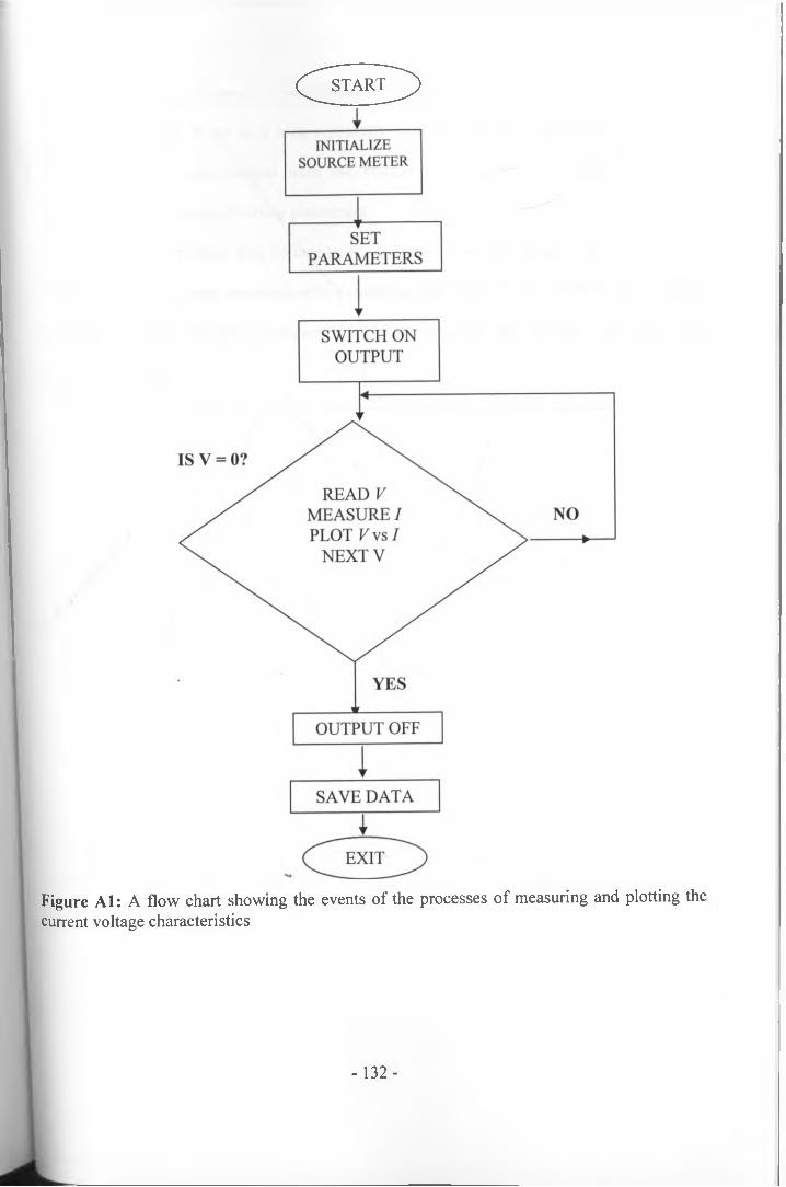
( ^ S T A R T ^ )
Figure Al: A flow chart showing the events of the processes of measuring and plotting the current voltage characteristics
- 132-

(d) Read Voltage, Measure Current and Plot graph
This process is carried out in a loop repeatedly until a condition is satisfied. A voltage is
sourced and the current excited from the voltage is measured. The sweep direction is
determined in the process of setting parameters
Voltage can be swept from zero voltage to Voc or from Voc to zero voltage. A while loop has
been used to execute these processes with a condition that while V is not equal to zero, perform
the source, measure and plot processes. If V = 0 the program exits the loop, saves data and
switches off output.

Appendix II
Automation of IP C E Characterization System
A2.0 Introduction
Revisiting the IPCE model equation earlier discussed in chapter 3, i.e.
IPCE(%) = x 100% (A-l)X.(nm)Pm(rnWcm 2)
where Jsc is the short circuit photocurrent density (measured by a source meter),
X is the wavelength (obtained from the lamp that is set at a particular wavelength by the
monochromator)
Pin is the incident radiation at a particular wavelength (obtained by an optical power meter and
a detector)
A plot of equation (4) gives a graph of IPCE (%) at different wavelengths (2).
The setup consists of a light source, a monochromator, a photodiode connected to an optical
meter and a current measurement system. To get the IPCE, first the incident power (P) is
measured at each wavelength and stored as a calibration file. The solar cell is then put at the
same position as the photodiode and current is measured at each wavelength. The calculation
of IPCE is accomplished by recalling the calibration file every time a new wavelength is set.
This process was automated using LabVIEW™ development application.
A2.1 Communication Protocol
(a) Monochromator
- 134-

The monochromator used here is Acton Research Corp. monochromator model
SpectraPro-150. Communication with this device was established via serial port
COM2. The commands for setting wavelength were processed through the dll
(dynamic link library) function call.
(b) Optical power meter
The optical power meter reads the power of incident light at a particular
wavelength set by the monochromator. The device is an Oriel Instruments OPM
model 70310. Communication was via GPIB interface with address 5. The
commands for reading out power from the instruments were established via
instrument drivers located in LabVIEW.
(c) Current Measurement
Current was measured by use of Keithley 2400™ source meter whose interface is
GPIB address 24. The commands for measuring current at the set wavelength are
via instrument drivers which are inside LabVIEW.
A2.2 Algorithm for Automating IPCE
The following is a summary of steps to be followed in the LabVIEW program for obtaining
IPCE automatically.
1. Obtain calibration data from optical power meter
2. Set the initial conditions (start and stop wavelengths)
3. Set wavelength required to the monochromator
4. Obtain current from the sample via Keithley source meter
-135-

5. Use the calibration data to incorporate in the IPCE formula for overall
calculation
6 . Plot IPCE vs X at the suitable steps
A2.3 Flowchart
A flowchart to implement the above algorithm is shown in figure 4.2 below
Figure A2: Flowchart for obtaining IPCE data from a solar cell.
-136-

Appendix III
Publications
- 137-

Journal of Electroanalytical Chemistry 646 (2010) 91-99
f V . , C - Vf c S r i , y O l ir% •£• • »
C ontents lists available at ScienceDirect
J o u r n a l o f E l e c t r o a n a l y t i c a l C h e m i s t r y
%
JllasiiUiUUi)ZiiMitUuj
E L S E V I E R j o u r n a l h o m e p a g e : w w w . e l s e v i e r . c o m / l o c a t e / j e l e c h e m S •
Interpretation of small-modulation photocurrent transients in dye-sensitized solar cells - A film thickness studyjarl Nissfolk3, Kristofer Fredinb, Justus Simiyuc, Leif Haggmanc, Anders Hagfeldta,c, Gerrit Boschlooc'*‘Center of Molecular Devices, Royal Institute of Technology, Chemical Science and Engineering, 10044 Stockholm, Sweden >Department of Physics and Materials Science, Uppsala University, Sweden cUppsala University, Dept, of Physical and Analytical Chemistry, Box 259, 751 05 Uppsala, Sweden
A R T I C L E i n f o A B S T R A C T
Article history:Received 1 O c to b e r 2 0 0 9
deceived in r e v i s e d f o rm 3 M a r c h 2 0 1 0
Accepted 1 5 M a rc h 2 0 1 0
Available o n l in e 1 8 M a rc h 2 0 1 0
tywords:Bectron transport tlesoporous T i02 Jffusion flapping
Electron transport in dye-sensitized solar cells with varying mesoporous Ti02 film thicknesses was investigated using experimental and computational methods. More specifically, photocurrent transients resulting from small-amplitude square-wave modulation of the incident light were recorded for a series of solar cells, whereby the dependence of the wavelength and direction of the illumination was investigated. The responses were compared to simulations using different models for diffusional charge transport and analyzed in detail. The photocurrent transients are composed of two components: an initial fast response in case of illumination from the working electrode side, or an initial apparent delay of photocurrent decay for illumination from the counter electrode side, followed by a single exponential decay at longer times, with a time constant that is identified as the electron transport time. The initial response depends on the thickness and the absorption coefficient of the film. Transport times for different films were compared at equal short-circuit current density, rather than at equal light intensity. Experimentally, the transport time showed a power-law dependence on the film thickness with an exponent of about 1.5. Analysis using the quasi-static multiple trapping (MT) formulation demonstrates that this behavior originates from differences in quasi-Fermi level in theTi02 films of different thickness when equal photocurrents are generated. The Fokker-Planck relation was used to derive expressions for the electrons flux in porous Ti02 films with a position-dependent diffusion coefficient.
© 2010 Elsevier B.V. All rights reserved.
Untroduction
Dye-sensitized solar cells (DSCs) have attained significant mention during the last years because of their potential to become flow-cost alternative to conventional solar cells. DSCs with an nerall power conversion efficiency exceeding 10% have been pre- tnted [1-5], Although the overall function of the device has been Wy well described [6-8], in-depth understanding of several pro- ®e$ is lacking. One of these, which is of central importance for * efficiency, is that of is electron transport in the electrolyte- filtrated mesoporous Ti02 film. It has been proposed by several ^Ps that this electron transport is driven by diffusion [9,10J. ’Perimental measurements as well as computer simulations have 5Played that the electron diffusion coefficient is related to the
I Wture of the mesoporous film [11] as well as the "necking" of TOoring nanoparticles [12,13]. Furthermore, it has been found
I electron diffusion coefficient is related to the composition electrolyte, via an ambipolar diffusion mechanism [14]. Fi-
f c [ * P O n d in g a u th o r . T e l .: + 4 6 1 8 4 7 1 3 3 0 3 .
address: g e r r i t .b o s c h lo o @ n < i .u u .s e (C . B o s c h lo o ) .
- see f r o n t m a t t e r © 2 0 1 0 E l s e v i e r B.V. A ll r ig h t s r e s e r v e d .
r ,0 l6 / j . je le c h e m .2 O 1 0 .0 3 .0 1 6
nally, the diffusion coefficient depends strongly on incident light intensity, as first reported by Cao et al. [15].
A number of experimental methods have been used to study the electron transport processes in mesoporous Ti02 films. Small- amplitude modulation methods such as intensity-modulated photocurrent spectroscopy (IMPS) [16-18] and transient photocurrent measurements [14,19] yield a transport time related to the electron diffusion coefficient. The transport time has been investigated as function of applied potential [20]. Charge transport measurements have also been conducted at open-circuit conditions using a transient voltage rise method [21], Electrical impedance spectroscopy (E1S) has been used to measure charge transport in mesoporous Ti02 electrodes, as well as complete DSCs [22,23], DC conductivity measurements of mesoporous Ti02 electrodes have been performed in redox inactive electrolytes [24], while conductivity measurements using microwave absorption [25] and terahertz spectroscopy [26] have been performed on mesoporous titanium dioxide systems in absence of electrolyte.
Experimental results have demonstrated that the measured (effective) diffusion coefficient is closely related to the total density of electrons and the quasi-Fermi level in the mesoporous Ti02 [22,23], This agrees well with the observations that the measured

J. Nissfolk et aL/Joumal of Electroanalytical Chemistry 646 (2010) 91-99
jery(IS-
nsp'
tron diffusion coefficient increases with light intensity in DSCs short-circuit conditions, as the quasi-Fermi level in the por-
fiC>2 is raised by the increased flux of photogenerated elec- i The electron transport and accumulation properties in
soporous Ti0 2 have been explained using a multiple trapping jjel, in which only a minor fraction of the electrons are being
orted in the conduction band, while most electrons are ■d in localized states below the band edge [27,28], The trap distribution can be related to the chemical capacitance of
nanostructured semiconductor [29], Computer simulations verified that the kinetics of the multiple trapping (MT) model lead to an anomalous electron transport process in accordance
^experimental results [30,31], Bisquert and Vihrenko demon- Jted that, when the kinetics of the trapping/detrapping process rj5ter than the time constant of the electron transport, a quasi
condition arises and that a chemical (effective) diffusion fficient can be defined that depends on the Fermi level [29], Imugh the MT model has gained acceptance within the scientific mnunity, it still lacks definite experimental proof. It has been nonstrated, using a theoretical model, that similar transport iracteristics can also be obtained when charge carriers are hop- between localized energy states [32], Recently, an overview of models that describe electron transport in semiconductors ha broad distribution of states was presented by Bisquert [33], Here, we will present results on transport time measurements j photocurrent transient method. The transient photocurrent ponse to a small square-wave modulation of light intensity is orded. It is demonstrated how the photocurrent response is meed by film thickness, illumination wavelength and illumi-
«n direction (from working electrode or counter electrode :).The relationship between electron transport time and meso- aus Ti02 film thickness was found to be more linear than ex- ied. The transport time would depend on the square of the thickness if the transport is described by a constant diffusion icient. The experimental results are compared with three lels using the diffusion model and the quasi-static approxima- of the MT model in the absence of recombination. We note Halme et al. recently studied similar issues using the IMPS
toique [34],
hperimental
Solar cell preparation
iiO; paste was prepared as described elsewhere [35], Working trades were prepared onto fluorine-doped tinoxide coated s(FT0) using the screen printing technique, yielding film thick- « between 4 and 26 pm. The area of the Ti02 films was 0.48 The electrodes were immersed in a dye bath containing
JiMN7 t 9 in ethanol overnight for sensitization. Counter elects Were created by spreading 5 mM F!2PtC!6 in isopropanol 1 (he FTO substrates (10pl/cm2), followed by heating to T-The DSCs were thereafter assembled by sealing the working ** counter electrodes with surlyn 1702 (~50 pm thickness) Producing the electrolyte via pre-drilled holes in the counter fode.The electrolyte was composed of 100 mM I2, 100 mM Lil,
tetrabutylammonium iodide and 500 mM 4-tert-butyl- lne- dissolved in 3-methoxypropionitrile.
V'octerization methods
...J"r°n transport measurements were performed by record- * Photocurrent response to a small square-wave modula- £ the light intensity [17,30]. Light emitting diodes
^ar l W) were used as the light source, giving red
(640 nm) and green (530 nm) light with intensities ranging from 0.2 to 32.5 mW cm-2 and 0.2 to 73.9 mW cm”2 for red and green light respectively. The RC-time constants of the solar cell
C 0-25
0.2
0 .1 5
X
h"0.1
0 .0 5
00 5 1 0 15 2 0 2 5 30
d I fi m
F ig . 1 . ( a ) N o r m a l i z e d d a t a o f s m a l l - a m p l i t u d e p h o t o c u r r e n t d e c a y t r a n s i e n t s o f
m e s o p o r o u s d y e - s e n s i t i z e d s o l a r c e l l s w i t h t w o f ilm th ic k n e s s e s , i l l u m i n a t e d f ro m
w o r k i n g e l e c t r o d e ( W E ) o r c o u n t e r e l e c t r o d e (C E ) s id e , ( b ) E le c t r o n t r a n s p o r t t im e
fo r t w o f i lm th i c k n e s s a s f u n c t i o n o f t h e s h o r t - c i r c u i t c u r r e n t d e n s i ty , ( c ) T r a n s p o r t
t im e fo r a r a n g e o f f i lm t h i c k n e s s e s c o m p a r e d a t Jx ■ 0 .5 m A c m - 2 , f o r W E a n d CE
i l l u m in a t io n .
# C E illumination X W E illumination
/ X %■ •
" " :

J. Nissfolk et ai/Joumal of Electroanalytical Chemisny 646 (2010} 91-99 93
Lere in the order of 0.1 ms and were neglected in the analysis of L e photocurrent transients.
, Simulations
Model calculations were performed using a finite element anal- rfjs, solver and simulation program (Femlab multiphysics 3.2 by qMSOL) on a laptop with Intel Pentium 1.7 GHz processor and
[Cb RAM. Simulation times ranged from 1 to 30 min.
1 Results and discussion
l| Experimental results
The influence of the carrier generation profile on the current insient during an electron transport experiment was studied by •ying the Ti02 film thickness, photon wavelength and illumina- idirection. In Fig. la, current transients are shown for two DSCs i film thicknesses of 6.9 and 19.8 pm, respectively, for green t illumination incident from either the working electrode side istrate-electrode (SE) illumination) or the counter electrode : (electrolyte-electrode (EE) illumination). As the normalized jtocurrents are plotted on a logarithmic scale versus time it is
1 seen that the photocurrent decays as a single exponential | longer timescales. In absence of significant recombination
is, the decay time constant equals the transport time, as will |shown later. On a shorter timescale, the current decay deviates
single exponential behavior. This deviation is most pro- inced for the thicker film for SE illumination (see Fig. la), lni- ly, the photocurrent decays faster, whereas for EE illumination [current remains constant for some time before it starts to de- |For the thinner Ti02 film, no discernable difference between
EE illumination can be observed. Repeating the measure- t with a red LED as light source gives similar photocurrent
[sients, however the initial deviations are less pronounced. This :to the lower absorption coefficient of the N719-sensitized
[film for red light, leading to more uniform electron generation ifilm, as will be discussed more in detail in Section 3.2.1.
Current transient measurements were performed for a range of [light intensities. The transport time, xIr, was extracted from [rate constant of the single exponential decay. It shows a tr-law dependence on the light intensity and the short-circuit intdensity, as illustrated in Fig. lb for two film thicknesses. A tr-law exponent of about -0.65 is determined from the slope.
ted, transport times are longer for thicker Ti02 films, nparison of the transport times for DSCs with different film iss was done under conditions of equal short-circuit photo- t density. For diffusion driven transport, this approach im-
Ijjjnilar gradients of the electron concentration profiles close I contact. It was therefore chosen over the light intensity ameter for comparison. For a short-circuit current density
JO-5 mA cm-2, the transport times are shown as function of 'ckness, d, in Fig. 1 c for SE and EE illumination. The r&lation 1 tfr and d is surprisingly linear. For electron transport dri-
Jdiffusion one would expect the transport time zn to vary ! square of the film thickness [36]. Instead, the data in
U'H'as best fitted with a power-law relation, t„-ocd“ , with ent w of 1.55 for EE and 1.32 for SE illumination.
1 vve will compare the presented results with predictions !°retical electron transport models based on pure diffusion
['land multiple trapping with the quasi-static approxima- a distance-independent or a distance dependent chem-
*®n coefficient (models 2 and 3, respectively). Effects of Ration will not be discussed here, but will be briefly ad- p th e supporting information.
3.2. Computational results and discussion
3.2.1. Pure diffusion (model 1)The simplest available electron transport model is that of diffu
sion of electrons with a constant diffusion coefficient in an effective medium [9], This implies that the diffusion coefficient, D, is not dependent on the concentration of electrons and effects related to trapping/detrapping. The photocurrent response in the time domain for the pure diffusion model has been solved analytically by Cao et al. for SE illumination [15], while the solution for the frequency-resolved analogue, i.e., IMPS, has been first reported by Peter and co-workers [16], The equations for the diffusion model are summarized in Appendix A.
During the electron transport measurements, the light intensity is increased and decreased by a step function Af0. giving rise to a photocurrent transient with amplitude AJ. In the experiment the DSC switches between two steady state situations; the difference in concentration of charge carriers between the two situations is AQ. As we describe transport diffusion, we only need to consider
3 12^1
10
<5
CD
CD
“ C E illumination a d « 1
■ • • C E illumination a d » 1 .... w e illumination a d » 1
— W E illumination a d « 1
4 6
x / Atm10
x 10
F ig . 2 . ( a ) G e n e r a t i o n p r o f i le o f e le c t r o n s C (x ) a t a d i s t a n c e x in t h e m e s o p o r o u s
T iO ; f i lm f r o m t h e c o n d u c t i n g s u b s t r a t e , n o r m a l iz e d b y t h e t o t a l a m o u n t o f
g e n e r a t e d c h a r g e c a r r i e r s , ( b ) T h e s t e a d y s t a t e e l e c t r o n c o n c e n t r a t i o n p r o f i le s in t h e
m e s o p o r o u s T i 0 2 a t t h e s a m e s h o r t - c i r c u i t c u r r e n t d e n s i t y ( 1 0 m A c m " 2 ) f o r p u r e
d i f f u s io n ( m o d e l 1 ; D * 1 0 s c m 2 s " ’ ) fo r t h e c a s e s I (ad - 0 .0 1 ) , II (ad - 1 0 ) a n d III (o d - 10).
V
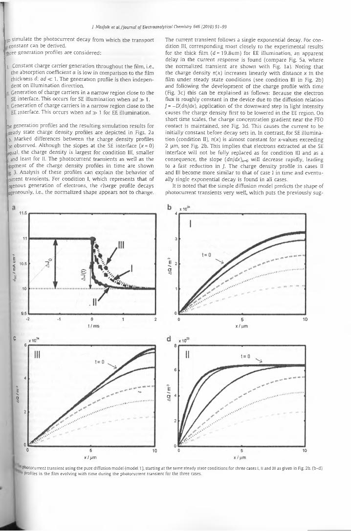
J. Nissfolk et al./Journal of Electroanalytical Chemistry 646 (2010) 91-99
i to simulate the photocurrent decay from which the transport constant can be derived,
three generation profiles are considered:
I. Constant charge carrier generation throughout the film, i.e., the absorption coefficient a is low in comparison to the film thickness d: ad « 1. The generation profile is then independent on illumination direction,
j. Generation of charge carriers in a narrow region close to the SE interface. This occurs for SE illumination when ad » 1.
(I Generation of charge carriers in a narrow region close to the EE interface. This occurs when ad » 1 for EE illumination.
;he generation profiles and the resulting simulation results for steady state charge density profiles are depicted in Figs. 2a b. Marked differences between the charge density profiles be observed. Although the slopes at the SE interface (x - 0) equal, the charge density is largest for condition III, smaller and least for II. The photocurrent transients as well as the
■lopment of the charge density profiles in time are shown ■g. 3. Analysis of these profiles can explain the behavior of current transients. For condition I, which represents that of ogenous generation of electrons, the charge profile decays ogeneously, i.e., the normalized shape appears not to change.
The current transient follows a single exponential decay. For condition 111, corresponding most closely to the experimental results for the thick film (d= 19.8um) for EE illumination, an apparent delay in the current response is found (compare Fig. 5a, where the normalized transient are shown with Fig. la). Noting that the charge density n(x) increases linearly with distance x in the film under steady state conditions (see condition III in Fig. 2b) and following the development of the charge profile with time (Fig. 3c) this can be explained as follows: Because the electron flux is roughly constant in the device due to the diffusion relation J=-D(dn/dx), application of the downward step in light intensity causes the charge density first to be lowered in the EE region. On short time scales, the charge concentration gradient near the FTO contact is maintained, see Fig. 3d. This causes the current to be initially constant before decay sets in. In contrast, for SE illumination (condition II), n(x) is almost constant for x-values exceeding 2 pm, see Fig. 2b. This implies that electrons extracted at the SE interface will not be fully replaced as for condition HI and as a consequence, the slope (dn/dx)*.0 will decrease rapidly, leading to a fast reduction in J. The charge density profile in cases II and 111 become more similar to that of case 1 in time and eventually single exponential decay is found in all cases.
It is noted that the simple diffusion model predicts the shape of photocurrent transients very well, which puts the previously sug-
x 10
x 10
x/pmP h o to c u r r e n t t r a n s i e n t u s i n g th e p u r e d i f f u s io n m o d e l ( m o d e l 1 ), s t a r t i n g a t t h e s a m e s t e a d y s t a t e c o n d i t i o n s f o r t h r e e c a s e s I, II a n d III a s g iv e n in Fig. 2 b . ( b - d )
v P ro fi le s in t h e f i lm e v o lv i n g w i t h t im e d u r i n g t h e p h o t o c u r r e n t t r a n s i e n t f o r t h e t h r e e c a s e s .

J. Nissfolk et al./Joumal of Electroanalyrical Chemistry 646 (2010) 91-99 95
I jested effect of non-thermalized electron transport in case of SE I illumination in question [30].
At longer times the photocurrent decay is described by Eq. (1), J independent on the illumination level and direction and absorp- I tjon coefficient:
|)(t) + A/■ e’i (la)
|fa " 2.47DLhereJ is the photocurrent density, and the constant bias level of |j.Similar expressions have been derived by others groups, although [slight differences in the factor 2.47 are reported, i.e. 2.35 [30] and |2.77 [37]. In our analysis we use an infinite lifetime of the electrons, making the approximation valid when the lifetime at short-circuit (condition is much longer than the transport time.
The transport time for the pure diffusion model is only related |to the thickness and the diffusion coefficient. The transport time tfjll not change with different intensities of bias light, which is in contradiction with the experimental results (see, e.g., Fig. lb). In |die following section trapping/detrapping of charge carriers is included in the model to account for this effect.
.2. Quasi-static multiple trapping model with distance-independent mical diffusion coefficient (model 2)The light intensity dependence of the electron transport time in isoporous dye-sensitized solar cells is successfully described by multiple trapping model [27,28], In this model, most electrons assumed to be trapped in localized energy states below the
induction band. Only a small fraction of the electrons is present the conduction band and can move by diffusion. There is a con-
pnuous exchange of electrons between traps and conduction band: iduction band electrons get trapped and trapped electrons are irmally excited back to the conduction band.The mathematics behind the multiple trapping model and its isi-static approximation are described in Appendix B. Here, only main outcomes are summarized: The diffusion coefficient mea- ed by small-amplitude transient techniques is not the diffusion fficient D0 of conduction band electrons, but a much smaller electron concentration dependent Dn, called the apparent or
mical diffusion coefficient [27,29,38]. Dn depends on the trap ite distribution and the occupation of the trap sites. In the case an exponential trap distribution, which will be assumed here, chemical diffusion coefficient depends on the electron concen- ion as described by Eq. (A17).Electron transport measurements in DSCs are normally per- ied at short-circuit conditions. Under these conditions the den-
>y of conduction band electrons is not constant in the film, but has Mient. It is, however, a reasonable approximation to take the Eduction band electron concentration (nc) as a constant, as nc % changes strongly close to the substrate. In model 2, the average 15determined from the nc profile that is calculated from the stea- state solution by using the pure diffusion model with D0 at a cer- ® short-circuit current density. In absence of recombination, the “rt-circuit current will be linearly dependent on light intensity in *Is 1 and 2. By increasing the light intensity, the number of con- ®°n band electrons will increase and hence also the chemical ’“sion coefficient D„. From Eq. (A5), it follows that the photocur-
is proportional to the average conduction band electron "% for both for SE and EE illumination. Using this relation with (Ai7 ), we fjnci the following relation between the chemical ls'°n coefficient and the short-circuit current density:
^ - r / T o (2a)
(2b)
Relation (2b), derived using the relationship between xn and a constant diffusion coefficient (Eq. (lb)), explains the power-law dependence of the transport time with short-circuit current. The value of T/T0 is easily determined from experimental data: from the slope in Fig. lb T/T0 is found to be 0.35 in the investigated DSCs.
The relation between transport time and film thickness was investigated using model 2. Fig. 4 shows how the conduction band electron density depends on film thickness, when the short-circuit current is held constant. There is a difference in the charge density profiles when changing the film thickness for the three illumination conditions. In case II (strong light absorption near the FTO contact), the average density of conduction band electrons remains almost constant when the thickness is changed, as nc is constant in the film except for a very narrow region near the SE interface. Consequently, the chemical diffusion coefficient remains constant and transport times scale with the square of the film thickness. For cases I and III, the average conduction band electron concentration scales linearly with film thickness. The measured transport time will depend both on the thickness and on the average charge density. The relation between xtr and d obtained from simulations with model 2 is:
zlr <x dff, with to = 2 for case II andco = 1 + T/To for cases 1 and III (3)
The photocurrent response will in all cases (I, II and III) have the same response as for pure diffusion (model 1), when rescaling the time by the transport time. This is because both models assume that diffusion coefficient is independent on the position in the film.
3.2.3. Quasi-static MT model with distance dependent chemical diffusion coefficient (model 3)
Under short-circuit conditions there is a gradient in the charge density in the porous Ti02 film, which gives rise to a chemical diffusion coefficient that depends on the position x in the film. In model 3, takes this distance dependence of D„ into account. In the quasi-static approximation of the MT model, the continuity equation is usually written in terms of conduction band electrons. Here, it will be shown that it may also be written in terms of total electron concentration.
A fundamental condition in Fick’s first law (used in models 1 and 2) is that diffusion coefficient is constant in the whole system.
F ig . 4 . T h e c h a r g e d e n s i t y p r o f i le s f o r c o n d u c t i o n b a n d e l e c t r o n s a t c o n s t a n t s h o r t -
c i r c u i t d e n s i t y , c a l c u l a t e d f o r t w o f ilm th i c k n e s s e s u s in g m o d e l 2 fo r c a s e s 1, II a n d
111.
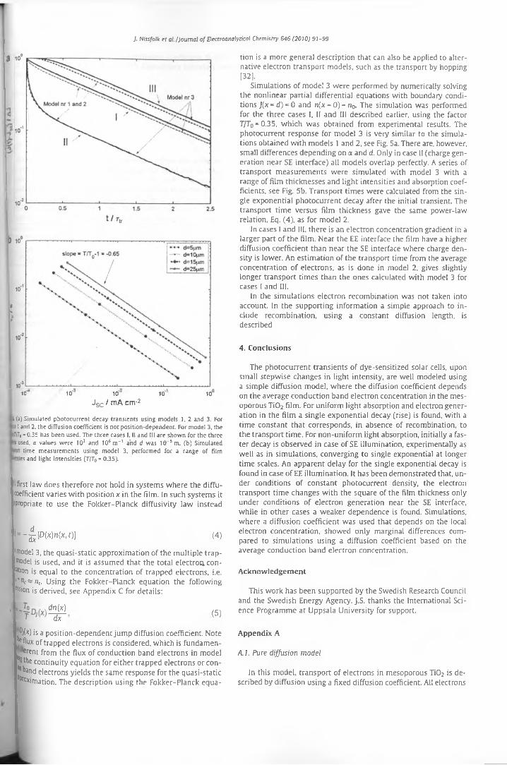
J. Nissfolk et ai/Journal of Electroanalyrical Chemistry 646 (2010) 91-99
10 10 10Jsc / mA crrv2
10 10
l (a) S im u la te d p h o t o c u r r e n t d e c a y t r a n s i e n t s u s in g m o d e l s 1 , 2 a n d 3 . F o r
s 1 a n d 2 , t h e d i f f u s io n c o e f f ic i e n t is n o t p o s i t i o n - d e p e n d e n t . F o r m o d e l 3 , t h e
!T;T0 - 0 .3 5 h a s b e e n u s e d . T h e t h r e e c a s e s I. II a n d III a r e s h o w n f o r t h e t h r e e
s used , a v a lu e s w e r e 1 0 3 a n d 1 0 6 m -1 a n d d w a s 1 0 5 m . ( b ) S i m u l a t e d
t im e m e a s u r e m e n t s u s in g m o d e l 3 , p e r f o r m e d f o r a r a n g e o f f ilm ies a n d l ig h t i n t e n s i t i e s (T /T 0 * 0 .3 5 ) .
•first law does therefore not hold in systems where the diffu- coefficient varies with position x in the film. In such systems it PPropriate to use the Fokker-Planck diffusivity law instead
l= “ ^ P M n(x,t)] (4)
'model 3, the quasi-static approximation of the multiple trap- model is used, and it is assumed that the total electron conation is equal to the concentration of trapped electrons, i.e. •+ric=snt. Using the Fokker-Planck equation the following ttsion is derived, see Appendix C for details:
dn(x)
dx(5)
P/*) is a position-dependent jump diffusion coefficient. NoteVflu* of trapped electrons is considered, which is fundamen-l efent from the flux of conduction band electrons in model \ th 8,1 ba"lithe continuity equation for either trapped electrons or con-
fPrc;jand electrons yields the same response for the quasi-staticIX|mation. The description using the Fokker-Planck equa
tion is a more general description that can also be applied to alternative electron transport models, such as the transport by hopping [32],
Simulations of model 3 were performed by numerically solving the nonlinear partial differential equations with boundary conditions J(x = d) = 0 and n(x = 0) = n0. The simulation was performed for the three cases 1, II and III described earlier, using the factor T/To = 0.35, which was obtained from experimental results. The photocurrent response for model 3 is very similar to the simulations obtained with models 1 and 2, see Fig. 5a. There are, however, small differences depending on a and d. Only in case II (charge generation near SE interface) all models overlap perfectly. A series of transport measurements were simulated with model 3 with a range of film thicknesses and light intensities and absorption coefficients, see Fig. 5b. Transport times were calculated from the single exponential photocurrent decay after the initial transient. The transport time versus film thickness gave the same power-law relation, Eq. (4), as for model 2.
In cases 1 and III, there is an electron concentration gradient in a larger part of the film. Near the EE interface the film have a higher diffusion coefficient than near the SE interface where charge density is lower. An estimation of the transport time from the average concentration of electrons, as is done in model 2, gives slightly longer transport times than the ones calculated with model 3 for cases 1 and III.
In the simulations electron recombination was not taken into account In the supporting information a simple approach to include recombination, using a constant diffusion length, is described
4. Conclusions
The photocurrent transients of dye-sensitized solar cells, upon small stepwise changes in light intensity, are well modeled using a simple diffusion model, where the diffusion coefficient depends on the average conduction band electron concentration in the mes- oporous Ti02 film. For uniform light absorption and electron generation in the film a single exponential decay (rise) is found, with a time constant that corresponds, in absence of recombination, to the transport time. For non-uniform light absorption, initially a faster decay is observed in case of SE illumination, experimentally as well as in simulations, converging to single exponential at longer time scales. An apparent delay for the single exponential decay is found in case of EE illumination. It has been demonstrated that, under conditions of constant photocurrent density, the electron transport time changes with the square of the film thickness only under conditions of electron generation near the SE interface, while in other cases a weaker dependence is found. Simulations, where a diffusion coefficient was used that depends on the local electron concentration, showed only marginal differences compared to simulations using a diffusion coefficient based on the average conduction band electron concentration.
Acknowledgement
This work has been supported by the Swedish Research Council and the Swedish Energy Agency. J.S. thanks the International Science Programme at Uppsala University for support.
Appendix A
A t Pure diffusion model
In this model, transport of electrons in mesoporous Ti02 is described by diffusion using a fixed diffusion coefficient. All electrons

J. Nissfolk er aL/Joumal of Blectroanalytical Chemistry 646 (2010) 91-99 97
are considered to be mobile with a diffusion coefficient D. Fick’s first law can therefore be applied with appropriate boundary conditions, Eqs. Al(a)-Al(c).
/(*) = -D dnc(x)dx
= 0x~d
(Ala)
(Alb)
*(0) = "o (Ale)](x) denotes the electron flux at position x from the substrate, nc
the electron concentration in the conduction band and n0 the conduction band electron concentration in the dark. The continuity equation with a source term for charge injection from the dye is given by Eq. (A2), where the generation profile, C(x) follows the Lam- tiert-Beer law and differs for electrolyte-electrode (EE) and substrate-electrode (SE) illumination. /0 is the photon flux of incident monochromatic light and a is the absorption coefficient at the same wavelength.
(A2)
_ f f0e-““ SE(A3)- \ Joe-z<*-d) £E
Note that this model does not include the recombination, which uld give an additional term in Eq. (A2). The continuity equations SE and EE illumination are:
iMc r,CPile;_ =D_ +„,oe (A4a)
(A4b)
These result in steady state solutions for given in Eq. (A5).JSc is short-circuit electron flux, equal to 70(1 - e~ad).
'»<(*) = Jsc (1 - oxe~ad - er
ocD (1 d )
:nc(x) =uD
,-cc(d-x) _ _ p -add)(1 - e-”1)
(A5a)
(A5b)
ndix B
'■ Multiple trapping model and quasi state approximation
In this model, traps with energies below the conduction band added. Electron transport takes place in the conduction band diffusion. During transport electrons will undergo numerous ?Ping and detrapping events. Detrapping is a thermally acti- *d process. Experimental results suggest that there is an^expo- *■*1 distribution of traps g(£j below the conduction band edge diat can be described by:
* j& o 6XP^£ ~ £c)/fc8T°5 (A6)
** is the total density of localized states and T0 is a parame- j dlated to the average depth of the distribution. The charge den-
electrons in the trapped states n, is calculated by integrating .ttte band gap states for a certain Fermi level £F(Eq. (A7)). Fer- **rac statistics (Eq. (AS)) are used to calculate the occupancy of tnergy levels.
n, = j \ ( E ) f , ( E ) (A7)
M E ) - | ~+ c( L f)/t.r (A8)
The density of conduction band electrons is given by the Boltzmann approximation:
nc = N c exp[(£F - Ec)/k„T] (A9)
It is assumed that electrons are not interacting and each energy level can be occupied by one electron. The resulting relation between trapped non-mobile electrons and mobile electrons in the conduction band is then
n, = N, exp[(Ef - Ec)/kBT0] = (AlOa)
nc NcNh(r n TofT (A10b)
The trapping model assumes that there is one single diffusion coefficient for the conduction band of electrons in the film, D0, which is independent of light intensity. The trapping/detrapping to and from the conduction band adds an additional factor to the continuity equation for diffusion:dn,~dt
-§Uc(x)dx v
dn,~dt (All)
where is the rate of change in concentration of trapped electrons per unit time, which is the sum of the trapping and detrapping kinetics described by Bisquert and Vikhrenko [29]. Under steady state illumination, the rates for trapping and detrapping are the equal and the number of conduction band electrons and trapped electrons are constant with time, so that ^ ^ = 0. The concentration of conduction band electrons in the multiple trapping model is equal to that of the pure diffusion model when the same diffusion coefficient for the conduction band electrons, D0, is used. When small modulations of light intensity are applied, both the number of conduction band electrons and trapped electrons change with time. The terms and ^ are then non-zero and electrons are being trapped and detrapped during the modulation. The kinetics involved in equilibrating the electrons in the conduction band and the trap states is a fast process. When this time is much faster than the measured quantity, in this case transport time for a small modulation of light, effects coming from equilibration may be neglected, which is the quasi-static approximation [29], When charge carriers in the traps and conduction band are in thermal equilibrium during the transition for the modulation, there is a relation between the rate of change in number of mobile charge carriers and non-mobile charge carriers [29]:On, _ On, Onc~dt~dncl>r (A12)
This is the so-called quasi-static condition. Eq. (A12) shows that the change of trapped electrons per unit time is directly related to the rate of change of the conduction band electrons at quasi equilibrium, being the case for fast trapping/detrapping kinetics. For the quasi-static and steady state situations the relation between charges in the traps and conduction band is given by Eq. (AlOb). The number of trapped electrons is considered to be much higher than the conduction band electrons, i.e. nc « n,. Therefore we can write the total number of electrons as trapped electrons n,0t = nc+ nt « nt. Using the quasi-static condition from A12 in Eq. (A ll) will form Eq. (A13)

J. Nissfolk et al. /Journal of Electroanalytical Chemistry 646 (2010) 91-99
3n,0n£ = _Q/ f+ t>nc Ot Ox U (A13)
F°r jt£ > > 1 FF1*5 equation can be re-written:0nc 0J 0nc
' * ' t o , 0 i + W tG{X)(A14a)
On, dx2 On,(A14b)
yje note that the generation term of the total amount of elec- ns is different from the generation term of conduction band ctrons §^G(x). The effective diffusion coefficient differs from from Eq. (AlOb) one can derive that:
Ntc/t°T0 : N-rT '
-T/To N J oN tT
exp (E-E,c)( k bT kbTo)
(Al 5)
Ifhe apparent electron diffusion coefficient measured by small- Ljlitude transient measurements methods is related to D0 as fol- *[29]:
dnc N Jo
"W,Do = W exp (E Ec)(k bT kbT0) (A16)
T0NTcrr°TN7
n’-T/T°D0 (A17)
-dixC
iffusion in inhomogeneous systems described ■ Fokker-Planck equation
transport of charge carriers can in very general terms be de- by kinetic or "jump" diffusion. The movement of carriers
place by random jumps between positions with spacing a a certain frequency r(n) that depends on the local carrier [ration. The jump diffusion coefficient Dj is given by:
\t{n)a2 (A18)
start by describing the movement between 3 positions in s 1, 2 and 3 with distance, a, between each position, see
1. The flux of charge carriers from position 3, with a concen- n3 to position 3 is J3.2 = n3 x r ( n 3) and from position 1 to 2 J1-2 = n, x r(n 3). The flux away from position 2 to the posi- 1 and 3 will cancel each other, J2-1 = -J 3-1. The macroscopic will then be J=Jj.2 - J 3-2-
<r(n,) - n 3 x r(n3) (Al 9)
can write this in terms of jump diffusion coefficient and concentration at any position x in the film. This results
Fokker-Planck equation (Eq. (A20)), which can be used for ’ eneous systems [39].
t e )n(x)] = _ ^ dnWdx dx J dx
(A20)
‘ case where the diffusion coefficient does not depend on ion, = 0, and Fields first law (Eq. (Ala)) is obtained,
diffusion coefficient for electrons in Ti02 depends on the concentration. As there is an electron concentration pro-
obtain a variation in the diffusion coefficient value in the quasi-static approximation of the multiple trapping
d't dependence of the chemical diffusion coefficient D„ on ^ncentration is given by Eq. (A17). If we test D/x) = D„ 7®r-Planck Eq. (A20), the flux equation appears as:
d jpro toj
F ig . A l . S c h e m a t ic s o f t h e c h a r g e c a r r i e r g e n e r a t i o n , c h a r g e t r a n s f e r b e tw e e n p a r t i c l e s a n d r e c o m b in a t io n .
m = -(y - = - t DjWt (A21)The flux is thus similar to that of pure diffusion except that the
diffusion coefficient is concentration dependent and that an additional constant factor appears. The factor is called the thermodynamic factor and originates from the presence of an electron concentration dependent diffusion coefficient [7,33,40], It can be seen that the jump diffusion, Dj, and the chemical diffusion coefficient, Dn differ by the thermodynamic factor:
Dn = j D j ( x ) (A22)
References
[1 ] B. O 'R e g a n , M . G r a tz e l , N a t u r e 3 5 3 ( 1 9 9 1 ) 7 3 7 .[2 ] M .K . N a z e e r u d d in , A. K ay . 1. R o d ic io , R. H u m p h r y - B a k e r , E. M u lle r . P. L isk a , N .
V la c h o p o u lo s , M . G rS tz e l . J. A m . C h e m . S o c . 1 1 5 ( 1 9 9 3 ) 6 3 8 2 .[3 ] M .K . N a z e e r u d d in . P . P e c h y ,T . R e n o u a r d , S .M . Z a k e e r u d d in , R. H u m p h r y - B a k e r ,
P. C o m te , P. L iska, L. C e v e y , E m il ia n a C o s ta , V . S h k lo v e r , L S p ic c ia , G.B. D e a c o n . C .A B ig n o z z i. M . G r a tz e l . J. A m . C h e m . S o c . 1 2 3 ( 2 0 0 1 ) 1 6 1 3 .
[4 ] A. H a g f e ld t , M . G r a tz e l , A cc. C h e m . R e s . 3 3 ( 2 0 0 0 ) 2 6 9 .[5 ] Y. C h ib a , A. I s la m , Y. W a ta n a b e , R. K o m iy a , N. K o id e , L H a n . J p n . J. A p p i. P h y s .
4 5 ( 2 0 0 6 ) 6 3 8 .[6 ] M . G r a tz e l , J. P h o to c h e m . P h o to b io l . C: P h o to c h e m . R ev . 4 ( 2 0 0 3 ) 1 4 5 .[7 ] J . B is q u e r t , D. C a h e n , G . H o d e s , S . R u h le , A . Z a b a n , J . P h y s . C h e m . B 1 0 8 ( 2 0 0 4 )
8 1 0 6 .[8 ] L M . P e te r , J . P h y s . C h e m . C 1 1 1 ( 2 0 0 7 ) 6 6 0 1 .|9 ] S. S d d e r g r e n , A. H a g f e ld t , J . O l s s o n , S.E . L in d q u is t , J. P h y s . C h e m . 9 8 ( 1 9 9 4 )
5 5 5 2 .[1 0 ] G . H o d e s , I.D .J. H o w e ll , L M . P e t e r , J . E l e c t r o c h e m . S o c . 1 3 9 ( 1 9 9 2 ) 3 1 3 6 .[1 1 ] K.D. B e n k s te in , N . K o p id a k is , j . V a n d e L a g e m a a t , A.J. F ra n k , J. P h y s . C h e m . B
1 0 7 ( 2 0 0 3 ) 7 7 5 9 .[ 1 2 ] K. F r e d in . S. R u h le , C. G r a s s o , A. H a g f e ld t , S o l. E n e r g y M a te r . S o l. C e lls 9 0 ( 2 0 0 6 )
1 9 1 5 .[ 1 3 ] M .J. C a s s , A.B. W a lk e r . D. M a r t in e z . L.M . P e te r . J . P h y s . C h e m . B 1 0 9 ( 2 0 0 5 )
5 1 0 0 .[ 1 4 ] N . K o p id a k is , E.A. S c h iff , N .G . P a r k , J. V a n d e L a g e m a a t , A.J. F ra n k , J. P h y s . C h e m .
B 1 0 4 ( 2 0 0 0 ) 3 9 3 0 .[1 5 ] F. C a o , G . O s k a m , P.C. S e a r s o n , J . P h y s . C h e m . 1 0 0 ( 1 9 9 6 ) 1 7 0 2 1 .[1 6 ] L. D lo c z ik , 0 . I l e p e r u m a . I. L a u e r m a n n , L P e te r , E. P o n o m a r e v . G . R e d m o n d . N.
S h a w . I. U h le n d o r f , J. P h y s . C h e m . B 1 01 ( 1 9 9 7 ) 1 0 2 8 1 .[1 7 ] P.E. d e J o n g h , D. V a n m a e k e l b e r g h , J. P h y s . C h e m . B 1 01 ( 1 9 9 7 ) 2 7 1 6 .[1 8 ] G . S c h l ic h th o r l , N .G . P a r k , A J . F r a n k . J . P h y s . C h e m . B 1 0 3 ( 1 9 9 9 ) 7 8 2 .[1 9 ] A. S o lb r a n d , H. L in d s tr o m , H . R e n s m o , A. H a g f e ld t , S.E. L in d q u is t . S . S d d e r g r e n ,
j . P h y s . C h e m . B 1 0 1 ( 1 9 9 7 ) 2 5 1 4 .[2 0 ] J. N is s fo lk , K. F r e d in . A. H a g f e ld t . G . B o s c h lo o , J. P h y s . C h e m . B 1 1 0 ( 2 0 0 6 )
1 7 7 1 5 .[2 1 ] B.C. O 'R e g a n . K. B a k k e r .J . K r o e z e , H . S m it , P. S o m m e l in g , J .R . D u r r a n t . J. P h y s .
C h e m . B 1 1 0 ( 2 0 0 6 ) 1 7 1 5 5 .[2 2 ] F. F a b r e g a t - S a n t i a g o , J. B i s q u e r t , G . G a r c ia - B e lm o n te , G . B o s c h lo o . A. H a g f e ld t ,
S o l. E n e r g y M a te r . S o l. C e lls 8 7 ( 2 0 0 5 ) 1 1 7 - 1 3 1 .[2 3 ] Q . W a n g , S. I to , M . G r a tz e l , F. F a b r e g a t - S a n t i a g o , 1. M o ra - S e r o , J . B is q u e r t , T.
B e s s h o , H . I m a i , J. P h y s . C h e m . B 1 1 0 ( 2 0 0 6 ) 2 5 2 1 0 .[2 4 ] H. C r e i je r - A g r e l l , G . B o s c h lo o , A . H a g f e ld t . J. P h y s . C h e m . B 1 0 8 ( 2 0 0 4 ) 1 2 3 8 8 .

J. Nissfolk et al./Joumal of Electroanalytical Chemistry 646 (2010) 91-99 99
[25] J.E . K ro e z e . T.J. S a v e n ije , J .M . W a r m a n , J. A m . C h e m . S o c . 1 2 6 ( 2 0 0 4 ) 7 6 0 8 .[26] E. H e n d r y . M . K o e b e rg , B. O 'R e g a n , M . B o n n , N a n o L e t t . 6 ( 2 0 0 6 ) 7 5 5 .2 7 ) A.C. F is h e r , L.M . P e te r , E A . P o n o m a r e v . A.B. W a lk e r , K .C .U . W i j a y a n th a , J. P h y s .
C h e m . B 1 0 4 ( 2 0 0 0 ) 9 4 9 .
[28] J. v a n d e U g e m a a t , A.J. F ra n k , J . P h y s . C h e m . B 1 0 4 ( 2 0 0 0 ) 4 2 9 2 .[29] J. B is q u e r t , V .S. V ik h r e n k o , J . P h y s . C h e m . B 1 0 8 ( 2 0 0 4 ) 2 3 1 3 .[30] J. v a n d e U g e m a a t , A.J. F ra n k , J . P h y s . C h e m . B 1 0 5 ( 2 0 0 1 ) 1 1 1 9 4 .[31 j J- N e ls o n , R. C h a n d le r , C o o rd . C h e m . R e v . 2 4 8 ( 2 0 0 4 ) 1 1 8 1 .[32] J. B is q u e r t . J. P h y s . C h e m . C 1 1 1 ( 2 0 0 7 ) 1 7 1 6 3 .[33] J. B is q u e r t , P h y s . C h e m . C h e m . P h y s . 1 0 ( 2 0 0 8 ) 3 1 7 5 .
[3 4 ] J . H a lm e . K. M ie t tu n e n , P . L u n d , J . P h y s . C h e m . C 1 1 2 ( 2 0 0 8 ) 2 0 4 9 1 .[ 3 5 ] P. W a n g , S .M . Z a k e e r u d d i n , P . C o m te , R. C h a r v e t , R. H u m p h r y - B a k e r , M .
C r a t z e l . J . P h y s . C h e m . B 1 0 7 ( 2 0 0 3 ) 1 4 3 3 6 .[ 3 6 ] A. S o lb r a n d , H . L in d s t r o m , H . R e n s m o , A . H a g f e ld t . S.E . L in d q u is t , S. S o d e r g r e n ,
J . P h y s . C h e m . B 10 1 ( 1 9 9 7 ) 2 5 1 4 .[ 3 7 ] S . N a k a d e . T . K a n z a k i, Y. W a d a , S. Y a n a g id a . U n g m u i r ( 2 0 0 5 ) 1 0 8 0 3 .[ 3 8 ] J . B i s q u e r t . J . P h y s . C h e m . B 1 0 8 ( 2 0 0 4 ) 2 3 2 3 .[ 3 9 ] B .P .v . M il l ig e n , P .D . B o n s . B A C a r r e r a s . R. S a n c h e z , E u r . ]. P h y s . 2 6 ( 2 0 0 5 ) 9 1 3 -
9 2 5 .
[ 4 0 ] J . v a n d e U g e m a a t . N . K o p id a k is , N.R. N e a le , A J . F ra n k , P h y s . R ev . B 71 ( 2 0 0 5 ) .

Mater. Res. Soc. Symp. Proc. Vol. 1171 © 2009 Materials Research Society 1171-S05-04
Conduction Band Edge of (Ti,Sn)02 Solid Mixtures Tuning for Photoelectrochemical Applications
J. Simiyu*, B. O. Aduda and J. M. Mwabora,
’University of Nairobi, Dept, of Physics, P.O. Box 30197 - 00100, Nairobi, Kenya
ABSTRACT
We report investigation of effect of conduction band edge on the dye injection and transport by preparation of (Ti,Sn)02 solid mixtures in ratios of 80:20 and 90:10 as possible applications in dye sensitized solar cells. SEM micrographs showed highly porous with nanometer sized particles of around 6 - 10pm diameter. X-ray diffraction patterns showed strong Ti02 anatase peaks with crystal orientation directions (101) being the strongest in both the solid mixtures and in pure Ti02. XPS studies have shown an apparent chemical shift for Ti 2p and Ols core level spectra with an energy difference between the unmodified and the solid mixture being 0.65eV. Initial I-V studies have shown high open circuit potential (Voc) but low short circuit photocurrent, showing a possible unfavorable band edge shift between the semiconductor and the dye LUMO level.
INTRODUCTION
Photoelectrochemical solar cells with wide-band-gap oxide semiconductors have received much attention since the development of dye-sensitized solar cell with porous Ti02 thin film by Gratzel’s group [1, 2], The chemical and physical processes involved in the operation of these cells take place in two-phase system consisting of porous Ti02 film and I3 /T redox electrolyte. Charge injection from the photoexcited dye and regeneration of the dye by electron transfer from T lead to transport of electrons in the Ti02 as well as transport of I3' and f ions in the electrolyte with electron transfer from I to the oxidized dye and regeneration of I from I3' at the counter electrode linking the two transport processes.
To achieve a favorable electron injection efficiency requires proper matching of the dye molecule’s LUMO (Lowest Unoccupied Molecular Orbital) level (in excited state) with the conduction band of the semiconductor. Various approaches have been applied, among them using dye molecules that have high LUMO levels in excited state, modifying the conduction band edge of the semiconductor to either lower or raise it [3 - 6 ] and using redox couples with high molecular orbital levels while maintaining the same band edge for the semiconductor. These studies have been done extensively on single semiconductors like Ti02, and to lesser extent ZnO and Sn02 [7, 8 ].
Recently dye sensitized nanoporous semiconductor materials comprising more than one material have been studied as a possible way to improve on performance [9-12], Tennakone et al. [13] reported the suppression of charge recombination for the mixture (referred to as composite) of Sn02 with small crystalline size of 15nm and ZnO with large crystalline size of 2 mm. Tai et al [14 - 16 ] studied widely Sn02-Ti02 coupled and composite solar cells using various sensitization dyes. They have reported higher values of Incident Photon to Current

conversion Efficiency (IPCE) in the coupled system compared with that of the composite system, attributing it to a better charge separation due to easy electron transfer in two semiconductor layers with different energy levels. These studies have been mainly on rutile type mixtures; however, anatase (Ti,Sn)02 solid mixtures have been reported before [17] but as potential applications in photocatalysis. An investigation of electron transport properties of these mixtures is of great importance for potential application in photovoltaics.
In the present study, sol-gel derived anatase nanostructured (Ti,Sn)02 solid mixtures were prepared at two ratios (80:20 and 90:10). The intention was to have Sn02 formed inside Ti02 hence only affecting the conduction band edge while maintaining crystal phase of the main semiconductor. Structural properties (SEM, ESCA & XRD) and electrochemical behavior were studied for the two ratios. Current voltage characteristics and electron transport studies were carried out on these solar cells.
EXPERIMENTAL DETAILS
The starting materials were titanium iso-propoxide (Ci2H2g04Ti), tin chloride precursors (SnCl4.5 H20 ), iso-propanol and 0.1M ammonia solution. All reagents were of analytical grade and were supplied by Sigma Aldrich unless stated otherwise. 7.4g of SnCL.5H20 was dissolved in 50ml iso-propanol then mixed with 60g titanium iso-propoxide. The resulting solution was then mixed drop wise slowly in 300ml of 0.1M NH3 under heavy stirring. This method produced instant precipitates, which was then heated to 80°C and peptized at that temperature for 8 hours. The precipitate was then cooled to room temperature and 250ml portion measured out and autoclaved at a temperature of 220°C for 12 hours. This resulted in (Ti,Sn)02 suspension of 6.22%wt which was further concentrated in rotor vapor to 20%wt concentration. Finally the paste was centrifuged and washed in ethanol three times to remove the salts and iso-propanol to produce (Ti,Sn)02 colloidal solution containing 40%wt. The (Ti,Sn)02 colloid in ethanol was then mixed with 2 0 .0g of tarpineol and further underwent stirring - sonication - stirring process. The same process was repeated after addition of 10% ethyl cellulose (Fluka GmbH, Germany) in ethanol to the colloid and then concentrated in a rotor vapor and collected in a reagent bottle. The resulting paste was about 21%wt of (Ti,Sn)02 solid mixture.
The above paste was used to coat films on F:Sn02 conducting glass substrate by screen printing method. The mesh size was 6 x8mm and one frame had 20 mesh openings that gave a total of 20 films at a single coating. To coat subsequent layers, the coated film was heated at a temperature of 150°C for five minutes and left to cool to room temperature then another coat applied until the required number of coatings was achieved. The films were then sintered in air for one hour at 450°C and left to cool to room temperature. These films were either used for XRD, SEM and ESCA analysis or assembled into complete solar cells for I-V, and transport/recombination analysis, after determining the film thickness. All films used in this study had 3pm film thickness.
X-Ray diffraction was obtained by means of Siemens D5000 Diffractometer (Bruker AXS GmbH, Germany) with 0-20 Parallel-beam geometry. The range was from 10° to 80° with detector type of scan at a scan speed of 0.6°/min and step size of 0.01°. (Ti,Sn)02 films for XRD analysis were coated on plain glass such that the Sn02 peaks observed are ascribed to the presence of Sn02 in the solid mixture. SEM micrographs were measured with LEO 1550 scanning electron microscope at 20kv electron source. ESCA spectra were recorded with

Quantum 2000 scanning ESCA probe (Physical Electronics Inc., USA) with A1 K<, x-ray source with photon energy of 1486.6eV.
Screen printed films were cut to a size of 3 x 2cm and heat treated at a temperature of 300°C for one hour to remove chemisorbed water and left to cool to 80°C and then subsequently immersed in a dye bath consisting of 0.5 mM ruthenium N719 dye complex in ethanol for 12 hours sensitization. Platinised counter electrodes were prepared by coating clean, predrilled conducting glass substrates (measuring 1.5 x 1.5cm), with 48mM of hydrochloroplatinic acid and heating the counter electrode at 450°C for 30 minutes in air and gradually cooled to room temperature. The dye sensitized (Ti,Sn)02 photoelectrode and counter electrode were then separated by a 25 pm thick thermoplastic surlyin film (DuPont, USA), and sealed by heating. The internal space having the dye sensitized nanoporous film was filled with a drop of the electrolyte through the two holes on the counter electrode. The electrolyte consisted of 0.1 M iodine, 0.1M LI, 0.6M TBA, 0.5M 4-terBPY in 3-methoxypropionitrile solvent medium. The electrolyte introduction holes were then sealed with another surlyn film under a thin glass cover by heating. Finally, silver was painted along the edges of the cell to make contacts and to reduce series resistance in the device.
I-V characteristics were obtained using Newport solar simulator model 91160 (Oriel Instruments, USA) to give an irradiation of 100mW/cm2 (equivalent of one sun at AM 1.5) at the surface of the solar cells. All the solar cells characterized in this work had an active area of 0.48cm . The current - voltage characteristics under these conditions were obtained by applying an external potential bias to the cell and measuring the generated current with a Keithley 2400 digital source meter (Keithley, USA). This process is fully automated using LabVDEW1 software from National Instruments Inc, USA.
The set up for electron transport and lifetime measurements consisted of Stanford Research Systems lock-in amplifier model SR 570 (Stanford Research Systems, USA), the HP 33120 function generator, and BNC 2110 data acquisition board (National instruments Inc, USA) controlled automatically by Lab VIEW™ (National Instruments Inc, USA) application. The light source was from a laser diode (LabLaser, Coherent LabLaser, USA) with 7 ^ 635nm. Switching from potentiostatic (to measure in short circuit) and galvanostatic (in open circuit) was achieved by use of a solid state switch. Electron transport and lifetime measurement followed a method developed by Boschloo et al. [18] for time resolved measurements. A small square wave modulation (<10% intensity, 0.1 - 2Hz) was added to the base light intensity. The solar cell response was fitted to exponential rise or decay function. Traces were averaged lOtimes for transport and 2 times for recombination studies.
RESULTS AND DISCUSSION
Structural Properties
From SEM analysis (Figure 1), the films produced were highly porous with nanometer sized particles. However, samples for solicFmixtures ((b) and (c)) had slightly smaller particle size than for pure Ti02 (d). This is possibly due to two main reasons, one being that the starting materials for both batches were different, i.e. pure Ti02 samples were made from P25 Degussa which has large particle sizes while the solid mixtures were made from titanium isopropoxide and the colloid particle size was determined by the autoclave temperature (which was 220°C). Another

possibility is that the presence of SnC>2 particles in the solid mixture may inhibit the growth of the colloid particles during autoclave digestion.
Figure 1: SEM scans for.(a) pure SnC>2, (b) 80:20 (Ti,Sn)02 solid mixture (c) 90:10 (Ti,Sn)02 solid mixture and (d) TiCh
This is because Ti0 2 colloids prepared from titanium isopropoxide (not shown in this work) have typical sizes ranging from lOnm to 30nm in diameter depending on the autoclave temperature. An increase in autoclave temperature to 250°C did not yield any meaningful rise in the particle size. From XRD analysis’ particle size determination using Scherer’s formula, pure Sn0 2 and solid mixtures gave particle sizes ranging from 6nm to lOnm. The size seemed not to affect dye sensitization as the solid mixtures showed very high dye attaching ability during sensitization. However, solar cells made from solid mixtures had very low Isc which does not agree with high dye attaching ability (thi&will be discussed in detail under IV results later in the report).
From XRD scans (Figure 2), strong anatase peaks from Ti02 were observed in solid mixture and in pure TiC>2 with crystal orientation directions (101) being the strongest. Previous works on solid mixtures have mainly produced rutile mixture, but in this work, solid mixtures in anatase form have been produced. Another aspect worth noting is that TiCh peaks in pure form do not show any peak shift in mixtures which suggests the absence of crystal phase change when SnC>2

and Ti0 2 are mixed. This is important because the only property in focus in solid mixtures is the variation of conduction band edge that should only affect the dye injection and not phase change that may affect the matching between Ti and Sn and hence the electron transfer during transport.
o
2 0 (degrees)Figure 2: XRD surface scans for pure (Ti,Sn)02 and 80:20 (Ti,Sn)02 solid mixtures. Bragg reflections with * are for Sn02 while the ones without are for Ti02.
However, at this point, it is not conclusively established that the solid mixture formed is a case where Sn forms within Ti shell and both form solid mixture oxide. XPS analysis so far earned out does not also show that. In Figure 2 for the case of mixtures, the strongest peak for Sn02 is in (101) direction but due to the small percentage composition compared to Ti02 it appears to be very small.

ESCA Results
From XPS studies (Figure 3), there is an apparent chemical shift for Ti 2p and Ols core level spectra (figures (c) and (d) on one hand and (e) and (f) on the other); with the energy difference between the unmodified and the solid mixture is found to be 0.65eV. Chemical shifts in Sn0 2 have been observed before [19], and have been attributed to possible change in Fermi level position in the semiconductor band gap or just due to band bending. This observation may be a similar occurrence in this case for Ti, which is very likely because it is also expected that Ols peaks shift with the same magnitude. From figures 3 (e) and (f), the energy shift is found to be 0.74eV which is within the range as of Ti 2p.
An interesting observation here is the absence of chemical shift in Sn 3d when mixed with Ti0 2 (Figures 3 (a) and (b)). This may partly confirm that Sn0 2 forms inside T1O2 shell which may only affect the conduction band edge while maintaining crystal phase of the main semiconductor (in this case Ti0 2 >. This property was earlier observed in XRD analysis in terms of phase shift.

Binding Energy (eV)Binding Energy (eV)
Binding Energy (eV) Binding Energy (eV)
Figure 3: Core level XPS scans for (a) Sn 3d in pure Sn02 (b) Sn 3d in 80:20 (Ti,Sn)02 mixture (c) Ti 2p in pure Ti02 (d) Ti 2p in 80:20 (Ti,Sn)02 mixture (e) O Is in Ti02 and (f) O Is in 80:20 (Ti,Sn)Q2 mixtures

I-V Characteristics
Figure 4 shows I-V characteristics for (Ti,Sn)(>2 solid mixture solar cells. Solar cell samples from this paste exhibited high Photovoltage but low photocurrent densities. The films showed very high dye adsorption during dye-sensitization, a property which is expected to translate to high electron harvesting and hence high photocurrent density; however that is not the case. This could therefore imply that the introduction of SnC>2 in the solid mixture could have raised the semiconductor conduction band edge instead of lowering it, making it hard for electrons to climb the energy barrier that is created. Further investigations are ongoing to ascertain the band edge position involving optical and I-V characterization. A change of the redox couple’s concentration from 0.1M LI & I to 0.5M showed an improvement in the photocurrent recorded (plot (b)). This could further indicate that the raise in concentration caused a shift in the conduction band more positive than when 0.1M was used.
Photovollage (mV)
Figure 4: I-V characteristics of (Ti02Sn)02 solid mixture films with different redox couple concentration
Electron Transport & Recombination Studies
Figure 5 shows electron transport and lifetime results for the solid mixture with 0.5M LI & I2 redox electrolyte couple; (a) shows the current transient obtained for the sample and (b) is the

transport time obtained from (a) plotted against the photocurrent at different diode light intensities.
(a)
Photocurrent (A) VJV)
(b) (c)
Figure 5. (a) Current transients for charge transport measurements, (b) transport time vs photocurrent and (c) electron lifetime vs photovoltage

The measured electron transport time (ttt) and lifetime (te) are shown as function of photocurrent (b) and photovoltage (c) respectively at various light intensities. An exponential relationship is obtained between ^ as reported before in other studies [18, 20, 21]. Samples exhibited long W times indicating slow transport process in the solid mixtures. One possible explanation for this is the inconsistent solid mixture formation which may lead to grain boundaries in the nanoporous structure. Another possible cause could be the formation of trap states in the solid mixtures. In general, electron lifetimes were longer than the transport times.
CONCLUSIONS
Sol-gel route has successfully been used here to produce titanium mixed oxide with anatase structure. XRD and ESCA studies have confirmed that mixed (Ti,Sn)02 was formed as a solid solution. It has been observed in this work that the particle size of the mixed oxide was smaller than that for the Ti0 2 obtained in a similar way. This has been observed before by Marcela et al[17] and from Leite and coworkers’ [19] report on a novel approach to control particle size of SnC>2 prepared by the polymeric precursor method, using NI32O5 as dopant. This effect was attributed to surface effect of the precursor, an effect that may be occurring in the present work, i.e presence of Sn0 2 restricting the growth to the surface.
Initial results have indicated that the use of 0.5M LI and 0.5M I2 raised the photocurrent density indicating that there was a shift in conduction band more positive than when 0.1M was used. This could have improved on electron injection in the system hence the increased photocurrent density. However, ESCA results have not conclusively shown that indeed solid mixture was formed with SnC>2 forming inside TiC>2, this leaves room for further work on this and also explore other methods of preparation of this mixtures. More important in the preparation step will be the stage at which precipitates form and when the mixtures are formed.
ACKNOWLEDGEMENTS
This research was performed at Angstrom Laboratory, Uppsala University, Sweden. Authors thank MSL, for SEM and ESCA, Material Chemistry for the X-ray diffractograms, Anders Hagfeldt Group for discussions and hosting me, International Science Programs (ISP) for the fellowship and thanks also to the University of Nairobi for granting me a study leave during this research.
REFERENCES
[1] B. O’Regan, M. Gratzel, Nature 353,737 (1991).[2] M.K. Nazeeruddin, A. Kay, I. Rodicio, R. Humphry-Baker, E. Muller, P. Liska, N.
Vlachopoulos, M. Gratzel, J. Am. Chem. Soc. 115, 6382 (1993).[3] R. Cavicchi, M. Tarlov and S. Semanchik, J. Vacc. Sci. Tech., A8 , 2347 (1990).[4] D.F. Cox, T.B., Fryberger and S. Semanchik, Surface Science, 224, 121(1989).[5] A. Ciera, A Comet, J.R, Morante, S.M. Oilaizola, E. Castino and J Gracia, Mater. Sci.
Eng. B, 66/70, 406 (2000).[6 ] J. Szuber, G. Czempic, R, Larcuprete and B Adamowicz, Sensors & Actuators B 65, 375
(2000).

[7] S.E. Lindquist, A. Hagfeldt, S. Sodergren, H. Lindstrom, in: G. Hodes (Ed.), Wiley, Weinheim, pp. 169-200 (2001).
[8 ] J.B. Asbury, E. Hao, Y. Wang, H.N. Gosh, T. Lain, J. Phys. Chem. B 105,4545 (2001).[9] C. Nasr, P.V. Kamat, S. Hotchandani, J. Phys. Chem. 102, 10047 (1998).[10] K. Tennakone, G.R.R.A. Kumara, I.R.M. Kottegoda, V.P.S. Perera, Chem. Commun.
1999 15 (1999).[11] K. Tennakone, J. Bandara, P.K.M. Bandaranayake, G.R.R.A. Kumara, A. Konno, Jpn. J.
Appl. Phys. 40L732 (2001)[12] G.R.R.A. Kumara, K. Tennakone, V.P.S. Perera, A. Konno, S. Kaneko, J. Phys. D: Appl.
Phys. 34 868 (2001).[13] K. Tennakone, P.K.M. Bandaranayake, P.V.V. Jayaweera, A. Konno, G.R.R.A. Kumara,
Physica E 14 190 - 196 (2002)[14] Weon-Pil, Tai, Kozo Inoue, Eosin Y-sensitized nanostructured SnCh/TiC solar cells,
Materials Letters 57 1508-1513 (2003).[15] Weon-Pil Tai, Solar Energy Materials & Solar Cells 76 65-73 (2003)[16] Weon-Pil Tai, Kozo Inoue, Jae-Hee Oh, Solar Energy Materials & Solar Cells 71 553-
557 (2002)[17] M. Marcela, D. Oliveira, C. Danielle, Schnitzler, and A.J. G. Zarbin, Chem. Mater. 15,
1903-1909(2003)[18] G. Boschloo, L. Haggman, A. Hagfeldt, J. Phys Chem B 110, 13144 (2006)[19] E.R Laite, I.T. Weber, E. Longo, J.A. Varela, Adv. Mater. 12, 965 (2000).[20] J. Nillsfolk, F. Kristofer, A. Hagfeldt, & G. Boschloo, J. Phys. Chem B, 110 (36), 17715
- 17718 (2006)[21] G. Schlichthorl, S. Huang, J. Sprague, A. Frank, J. Phys Chem B 101, 8141. (1997)

African Physical Review (2008) 2 Special Issue (Materials): 0083 161
Titania Nanotubes Prepared by Synthesis Method for Dye Sensitized Electrochemical Solar Cells
J. Simiyu1, J. M. Mwabora1, B. O. Aduda1, S-E. Lindquist2, A. Hagfeldt2 and G. Boschloo 'University o f Nairobi, Nairobi, Kenya
2 Uppsala University, Department o f Physical Chemistry, Uppsala, Sweden
2
1. Introduction
The area of nanostructured materials for dye sensitized solar cells has gained great interest especially after a breakthrough by Gratzel and coworkers in developing a solar cell from nanostructured oxide of titania gaining an overall efficiency of about 11% [1-5]. Since then the research has been going on with an emphasis on further improvement on this achievement [6-8],
One area that is having a lot of interest is improvement on the charge transfer characteristics from the dye to semiconductor and hence in the whole system. The approach in our research group has been on synthesis of nanofibers of titania oxide that can provide a directed transport of electrons to the conducting back contact and hence giving optimal electronic charge transport through the cell. Titania nanofibers have been synthesised before [9-11], but the reports have been inconclusive as to what stage of synthesis the nanofibers form.
2. Main results
Ti02 nanofibers measuring average length 500nm and diameter lOnm have been prepared by synthesis method using 10M NaOH and dispersed in alcohol (Fig. la). Thin films prepared from the nanofibers had thickness varying from 4.5 - 5.5pm. The films were used to fabricate complete dye sensitised solar cells with Ruthenium complex dye as sentizer. I-V characteristics yielded Voc and Isc of 0.41V - 0.58V and 0.18mA - to 1.1mA, respectively, under standard illumination of 100mW/cm2 (using a halogen lamp and data acquired using Keithley 2400 Source Metre® controlled by LabVIEW® software) (Fig. 1 b). XRD analysis indicated strong anatase peaks with crystal orientation in the direction (101). This showed that there was no loss of crystalline structure of the Ti02 during the synthesis process. However, as the sintering temperature was raised, the percentage crystal content of anatase reduced as the rutile structure slowly formed.
(b)
Fig. 1: TEM images for titania nanotubes autoclaved at 500°C (a) in purified water and (b) corresponding I-V
characteristics.
3. C onclusion
Initial results have indicated that nanotubes of TiC^ can be produced by synthesis method and it has also been seen that nanotube formation occurs at the rinsing stage. However, TEM results have not shown conclusively whether the nanotube profile is in tubular form with cylindrical profile or a solid profile. This report has also demonstrated that titanium dioxide nanotubes can be a potential material for solar cells.

African Physical Review (2008) 2 Special Issue (Materials): 0083 162
References
[1] M. Gratzel and B. O'Regan, Nature 353, 737 (1991).
[2] M. Gratzel and A. Hagfeldt, Chem. Rev. 95, 49 (1995).
[3] M. Gratzel, T. Gerfin and L. Walder, Chem. Rev. 44, 345(1997).
[4] M. K. Nazeeruddin, A. Kay, I. Rodicho, Humphry-aker, E. Muller, P. Liska, N. Vlachopoulos, and M. Gratzel, J. Am. Chem. Soc. 115, 6382 (1993).
[5] V. Aranyos, H. Grennberg, S. Tingry, S-E. Lindquist and A. Hagfeldt, Solar Energy Materials and Solar Cells 64, 97 (2000).
[6] L. Hammastrom, J. Alsins, A. Botje, T. Norry, L. Zhang and B. Akermark, J. Photochem. & Photobio!. 102, 139 (1996).
[7] N. J. Cherapy, P. Smestad, M. Gratzel and J. Zhang, J. Phys. Chem. B 101,9342 (1997).
[8] G. Smestad, Solar Energy Materials and Solar Cells 55, 157(1998).
[9] T. Kasuga, M. Hiramatsu, A. Hoson, T. Sekino and K. Niira, Advanced Materials 11, 1307(1999).
[10] Y-K. Zhou, L. Cao, F.-B. Zhang, B-L. He and H-L. Li, J. Electrochemical Society 150 (9), A1246 (2003).
[11] Y. D. Li and X. M. Sun, Chem. Eur. J. 9,2229 (2003).
v