chapter iii quantum transport in nanostructures · 1 nm ↔ 10.000 k ↔ 800 mev ... source:...
TRANSCRIPT
Chapter III
Quantum Transportin
Nanostructures

Chapt. III - 2
R. G
ross
and
A. M
arx
, © W
alth
er-
Me
ißn
er-
Inst
itu
t (2
00
4 -
20
15
)
Contents:
III.1 IntroductionIII.1.1 General RemarksIII.1.2 Mesoscopic SystemsIII.1.3 Characteristic Length ScalesIII.1.4 Characteristic Energy ScalesIII.1.5 Transport Regimes
III.2 Description of Electron Transport by Scattering of WavesIII.2.1 Electron Waves and WaveguidesIII.2.2 Landauer FormalismIII.2.3 Multi-terminal Conductors
III.3 Quantum Interference EffectsIII.3.1 Double Slit ExperimentIII.3.2 Two Barriers – Resonant TunnelingIII.3.3 Aharonov-Bohm EffectIII.3.4 Weak LocalizationIII.3.5 Universal Conductance Fluctuations
III.4 From Quantum Mechanics to Ohm‘s Law
III.5 Coulomb Blockade
Chapter III: Quantum Transport in Nanostructures

Chapt. III - 3
R. G
ross
and
A. M
arx
, © W
alth
er-
Me
ißn
er-
Inst
itu
t (2
00
4 -
20
15
)
Literature:
1. Introduction to Mesoscopic PhysicsYoseph ImryOxford University Press, Oxford (1997)
2. Electronic Transport in Mesoscopic SystemsSupriyoto DattaCambridge University Press, Cambridge (1995)
3. Mesoscopic Electronic in Solid State NanostructuresThomas HeinzelWiley VCH, Weinheim (2003)
4. Quantum TransportYuli V. Nazarov, Yaroslav M. BlanterCambridge University Press, Cambridge (2009)
Chapter III: Quantum Transport in Nanostructures
Chapt. III - 4
R. G
ross
and
A. M
arx
, © W
alth
er-
Me
ißn
er-
Inst
itu
t (2
00
4 -
20
15
)
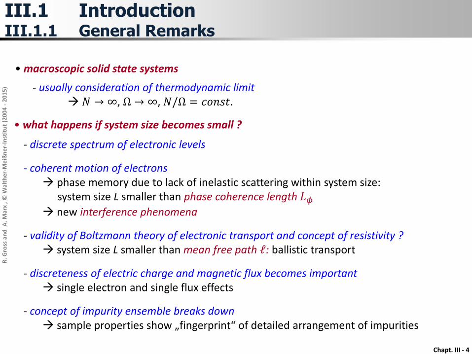
• macroscopic solid state systems
- usually consideration of thermodynamic limit 𝑁 → ∞, Ω → ∞, 𝑁/Ω = 𝑐𝑜𝑛𝑠𝑡.
• what happens if system size becomes small ?
- discrete spectrum of electronic levels
- coherent motion of electrons phase memory due to lack of inelastic scattering within system size:
system size L smaller than phase coherence length 𝐿𝜙
new interference phenomena
- validity of Boltzmann theory of electronic transport and concept of resistivity ? system size L smaller than mean free path ℓ: ballistic transport
- discreteness of electric charge and magnetic flux becomes important single electron and single flux effects
- concept of impurity ensemble breaks down sample properties show „fingerprint“ of detailed arrangement of impurities
III.1 IntroductionIII.1.1 General Remarks
Chapt. III - 5
R. G
ross
and
A. M
arx
, © W
alth
er-
Me
ißn
er-
Inst
itu
t (2
00
4 -
20
15
)
• mesoscopic systems (coined by Van Kampen in 1981):
- system size is between microscopic (e.g. atom, molecule) andmacroscopic system (e.g. bulk solid)
- system size L is smaller than phase coherence length 𝐿𝜙 (typically in nm - µm regime)
quantum coherent phenomena become important statistical concepts no longer applicable due to smallness of system size still coupling to environment/reservoir present
(in contrast to microscopic objects such as atoms)
study of nanostructures at low temperature
mesos (Greek): between
• properties of mesoscopic systems are usually studied at low temperatures
- phase coherence length 𝐿𝜙 decreases rapidly with increasing T
𝐿 < 𝐿𝜙 can usually be satisfied only at low T
- observation of level quantization effects require 𝑘𝐵𝑇 < Δ𝐸 ≃ 1/𝐿2
III.1 IntroductionIII.1.2 Mesoscopic Systems

Chapt. III - 6
R. G
ross
and
A. M
arx
, © W
alth
er-
Me
ißn
er-
Inst
itu
t (2
00
4 -
20
15
)
III.6
III.1 IntroductionIII.1.2 Mesoscopic Systems – The World of Solid State Nanostructures
Chapt. III - 7
R. G
ross
and
A. M
arx
, © W
alth
er-
Me
ißn
er-
Inst
itu
t (2
00
4 -
20
15
)
III.1 IntroductionIII.1.2 Mesoscopic Systems – Fabrication of Single Electron Device

Chapt. III - 8
R. G
ross
and
A. M
arx
, © W
alth
er-
Me
ißn
er-
Inst
itu
t (2
00
4 -
20
15
)
superconducting flux quantum circuit

Chapt. III - 9
R. G
ross
and
A. M
arx
, © W
alth
er-
Me
ißn
er-
Inst
itu
t (2
00
4 -
20
15
)
65 nm process2005
45 nm process2007 32 nm
2009 22 nm2011
(Source: Intel Inc.)
gate length of transistors
III.1 IntroductionIII.1.2 Mesoscopic Systems – Miniaturization of Electronic Devices

Chapt. III - 10
R. G
ross
and
A. M
arx
, © W
alth
er-
Me
ißn
er-
Inst
itu
t (2
00
4 -
20
15
)
Fermi wave length: 𝜆𝐹 < 1 nm (for metals)
”size” of charge carrier
electron mean free path: ℓ 10 - 100 nm
distance between (elastic) scattering events
phase coherence length: 𝐿𝜑 1 mm
loss of phase memory
sample size: 𝐿, 𝑊 0.01 - 1 mm
microscopic mesoscopic macroscopic
mesoscopic regime: L < Lj (T)
from microscopic to macroscopic systems
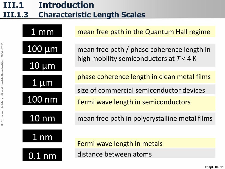
III.1 IntroductionIII.1.3 Characteristic Length Scales
Chapt. III - 11
R. G
ross
and
A. M
arx
, © W
alth
er-
Me
ißn
er-
Inst
itu
t (2
00
4 -
20
15
)
10 µm
1 mm
100 µm
1 µm
100 nm
10 nm
1 nm
0.1 nm distance between atoms
Fermi wave length in metals
mean free path in polycrystalline metal films
Fermi wave length in semiconductors
size of commercial semiconductor devices
mean free path in the Quantum Hall regime
mean free path / phase coherence length inhigh mobility semiconductors at T < 4 K
phase coherence length in clean metal films
III.1 IntroductionIII.1.3 Characteristic Length Scales

Chapt. III - 12
R. G
ross
and
A. M
arx
, © W
alth
er-
Me
ißn
er-
Inst
itu
t (2
00
4 -
20
15
)
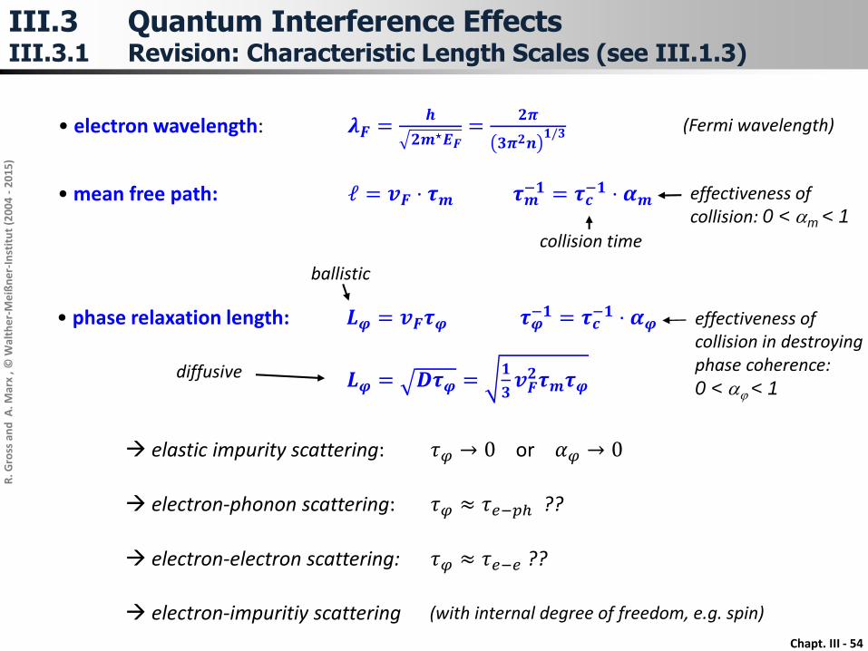
elastic impurity scattering: 𝜏𝜑 → 0 or 𝛼𝜑 → 0
electron-phonon scattering: 𝜏𝜑 ≈ 𝜏𝑒−𝑝ℎ ??
electron-electron scattering: 𝜏𝜑 ≈ 𝜏𝑒−𝑒 ??
electron-impuritiy scattering
• electron wavelength: 𝝀𝑭 =𝒉
𝟐𝒎⋆𝑬𝑭=
𝟐𝝅
𝟑𝝅𝟐𝒏𝟏/𝟑 (Fermi wavelength)
collision time
effectiveness ofcollision: 0 < am < 1
• mean free path: ℓ = 𝒗𝑭 ⋅ 𝝉𝒎 𝝉𝒎−𝟏 = 𝝉𝒄
−𝟏 ⋅ 𝜶𝒎
III.1 IntroductionIII.1.3 Characteristic Length Scales
(with internal degree of freedom, e.g. spin)
• phase relaxation length: 𝑳𝝋 = 𝒗𝑭𝝉𝝋 𝝉𝝋−𝟏 = 𝝉𝒄
−𝟏 ⋅ 𝜶𝝋 effectiveness ofcollision in destroyingphase coherence: 0 < aj < 1
ballistic
diffusive 𝑳𝝋 = 𝑫𝝉𝝋 =𝟏
𝟑𝒗𝑭
𝟐𝝉𝒎𝝉𝝋

Chapt. III - 13
R. G
ross
and
A. M
arx
, © W
alth
er-
Me
ißn
er-
Inst
itu
t (2
00
4 -
20
15
)
• Altshuler, Aronov, Khmelnitsky (1982):
if ħw is characteristic energy of an inelastic process (e.g. phonon energy),then the mean-squared energy spread of electron after collision is
• question: what is the effectiveness of an inelastic scattering processregarding destruction of phase coherence ?
square of energy change
number of scattering events
• at low T: e-e scattering is dominating
III.1 IntroductionIII.1.3 Characteristic Length Scales
Δ𝐸 2 = ℏ𝜔 2𝜏𝜑
𝜏𝑐
low-frequencyexcitationsare less effective indestroying phasecoherence !!
𝜏𝜑 is time required to acquire a phase change of ≈ 2p
Δ𝜑 ≈Δ𝐸
ℏ𝜏𝜑 ≈ 2𝜋 ⇒ 𝜏𝜑 ≈
𝜏𝑐
𝜔2
1/3
Chapt. III - 14
R. G
ross
and
A. M
arx
, © W
alth
er-
Me
ißn
er-
Inst
itu
t (2
00
4 -
20
15
)
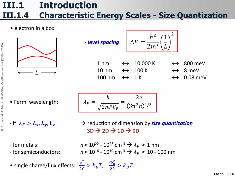
• Fermi wavelength:
- if 𝝀𝑭 > 𝑳𝒙, 𝑳𝒚, 𝑳𝒛 reduction of dimension by size quantization
3D 2D 1D 0D
- for metals: n ≈ 1022 - 1023 cm-3 𝜆𝐹 ≈ 1 nm
- for semiconductors: n ≈ 1016 - 1019 cm-3 𝜆𝐹 ≈ 10 - 100 nm
• electron in a box:
- level spacing:
1 nm ↔ 10.000 K ↔ 800 meV10 nm ↔ 100 K ↔ 8 meV100 nm ↔ 1 K ↔ 0.08 meV
L
• single charge/flux effects: 𝑒2
2𝐶> 𝑘𝐵𝑇,
Φ02
2𝐿> 𝑘𝐵𝑇
III.1 IntroductionIII.1.4 Characteristic Energy Scales - Size Quantization
Δ𝐸 =ℎ2
2𝑚⋆
1
𝐿
2
𝜆𝐹 =ℎ
2𝑚⋆𝐸𝐹
=2𝜋
3𝜋2𝑛 1/3

Chapt. III - 15
R. G
ross
and
A. M
arx
, © W
alth
er-
Me
ißn
er-
Inst
itu
t (2
00
4 -
20
15
)
quantum wire
1-dim
bulk
3-dim
superlattice
D(E)
E
quantum well
D(E)
E
2-dim
quantum dot
0-dim
const ED )(
D(E)
E
EED )(
D(E)
E
EED /1)(
D(E)
E
)()( iEE ED
III.1 IntroductionIII.1.4 Size Quantization – DOS in 3D, 2D, 1D, and 0D
Chapt. III - 16
R. G
ross
and
A. M
arx
, © W
alth
er-
Me
ißn
er-
Inst
itu
t (2
00
4 -
20
15
)
L
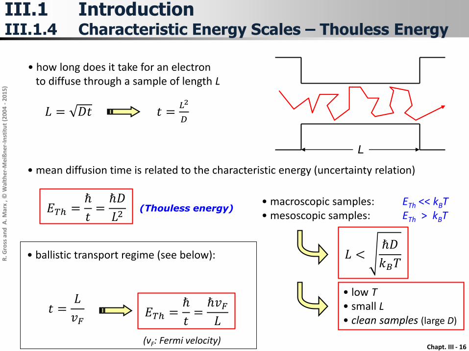
• how long does it take for an electronto diffuse through a sample of length L
(Thouless energy)• macroscopic samples: ETh << kBT• mesoscopic samples: ETh > kBT
• low T• small L• clean samples (large D)
• mean diffusion time is related to the characteristic energy (uncertainty relation)
III.1 IntroductionIII.1.4 Characteristic Energy Scales – Thouless Energy
𝐿 = 𝐷𝑡 𝑡 =𝐿2
𝐷
𝐸𝑇ℎ =ℏ
𝑡=
ℏ𝐷
𝐿2
(vF: Fermi velocity)
• ballistic transport regime (see below):
𝑡 =𝐿
𝑣𝐹𝐸𝑇ℎ =
ℏ
𝑡=
ℏ𝑣𝐹
𝐿
𝐿 <ℏ𝐷
𝑘𝐵𝑇
Chapt. III - 17
R. G
ross
and
A. M
arx
, © W
alth
er-
Me
ißn
er-
Inst
itu
t (2
00
4 -
20
15
)
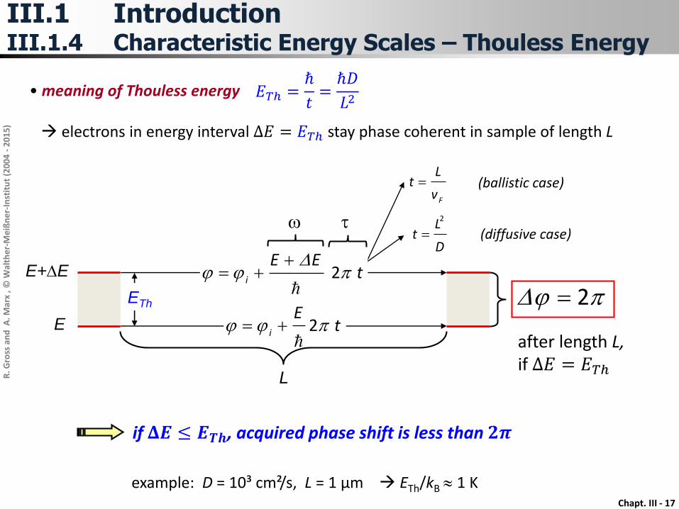
• meaning of Thouless energy
electrons in energy interval Δ𝐸 = 𝐸𝑇ℎ stay phase coherent in sample of length L
E+DE
E
Fv
Lt
D
Lt
2
(ballistic case)
(diffusive case)
ETh
tE
i 2 pjj
tEE
i 2 pD
jj
L
pjD 2
if 𝚫𝑬 ≤ 𝑬𝑻𝒉, acquired phase shift is less than 𝟐𝝅
III.1 IntroductionIII.1.4 Characteristic Energy Scales – Thouless Energy
w t
after length L,if Δ𝐸 = 𝐸𝑇ℎ
example: D = 10³ cm²/s, L = 1 µm ETh/kB 1 K
𝐸𝑇ℎ =ℏ
𝑡=
ℏ𝐷
𝐿2
Chapt. III - 18
R. G
ross
and
A. M
arx
, © W
alth
er-
Me
ißn
er-
Inst
itu
t (2
00
4 -
20
15
)
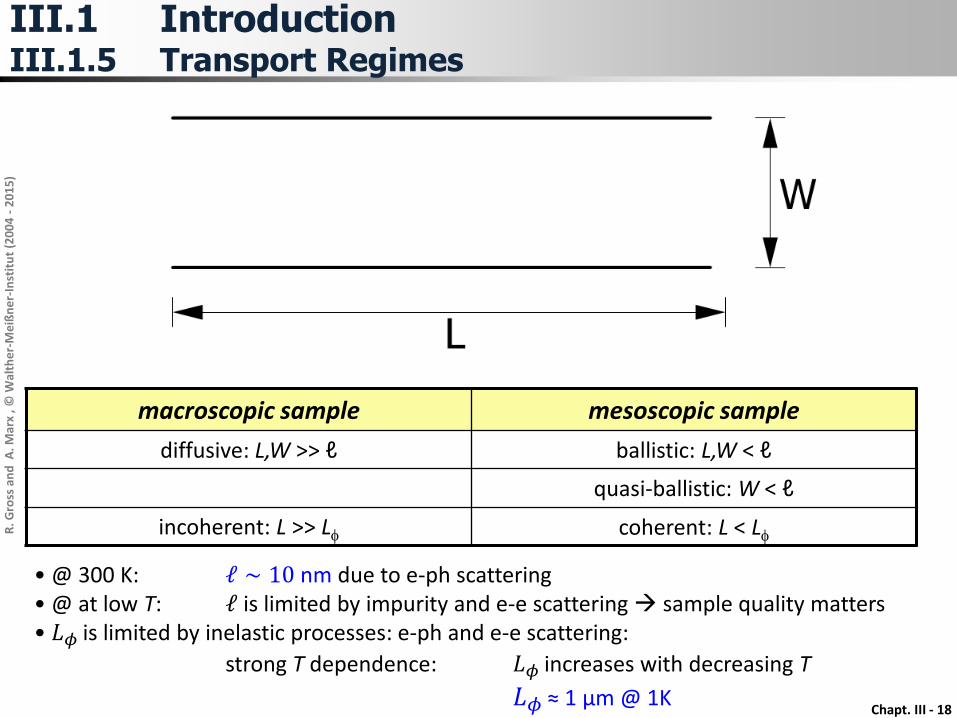
macroscopic sample mesoscopic sample
diffusive: L,W >> ℓ ballistic: L,W < ℓ
quasi-ballistic: W < ℓ
incoherent: L >> Lf coherent: L < Lf
• @ 300 K: ℓ ∼ 10 nm due to e-ph scattering• @ at low T: ℓ is limited by impurity and e-e scattering sample quality matters• 𝐿𝜙 is limited by inelastic processes: e-ph and e-e scattering:
strong T dependence: 𝐿𝜙 increases with decreasing T
𝐿𝜙 ≈ 1 µm @ 1K
III.1 IntroductionIII.1.5 Transport Regimes
Chapt. III - 19
R. G
ross
and
A. M
arx
, © W
alth
er-
Me
ißn
er-
Inst
itu
t (2
00
4 -
20
15
)
Contents:
III.1 IntroductionIII.1.1 General RemarksIII.1.2 Mesoscopic SystemsIII.1.3 Characteristic Length ScalesIII.1.4 Characteristic Energy ScalesIII.1.5 Transport Regimes
III.2 Description of Electron Transport by Scattering of WavesIII.2.1 Electron Waves and WaveguidesIII.2.2 Landauer FormalismIII.2.3 Multi-terminal Conductors
III.3 Quantum Interference EffectsIII.3.1 Double Slit ExperimentIII.3.2 Two Barriers – Resonant TunnelingIII.3.3 Aharonov-Bohm EffectIII.3.4 Weak LocalizationIII.3.5 Universal Conductance Fluctuations
III.4 From Quantum Mechanics to Ohm‘s Law
III.5 Coulomb Blockade
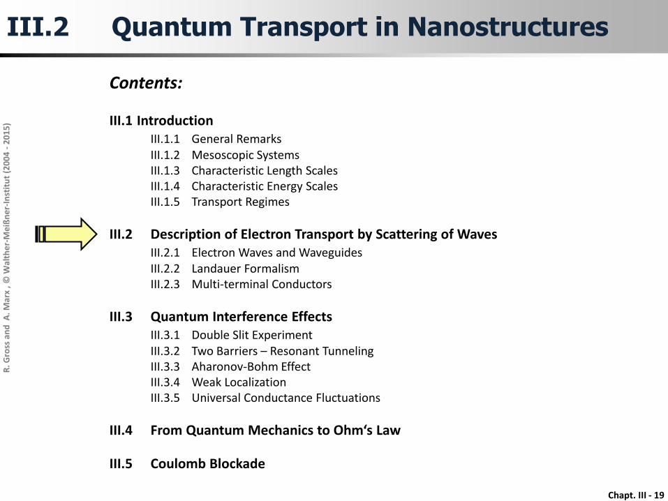
III.2 Quantum Transport in Nanostructures

Chapt. III - 20
R. G
ross
and
A. M
arx
, © W
alth
er-
Me
ißn
er-
Inst
itu
t (2
00
4 -
20
15
)
• electrons as plane waves (true only in vacuum)
wave function
probability to find electron at position 𝐫 at time 𝑡
normalization volume
wave vector
momentum
energy
tkE
ii
Vt )(exp
1),(
rkr
),( tr
2),( tr
V
k
kp
m
kE
2
22
III.2 Description of Electron Transport by Scattering of WavesIII.2.1 Electron Waves and Waveguides
Chapt. III - 21
R. G
ross
and
A. M
arx
, © W
alth
er-
Me
ißn
er-
Inst
itu
t (2
00
4 -
20
15
)
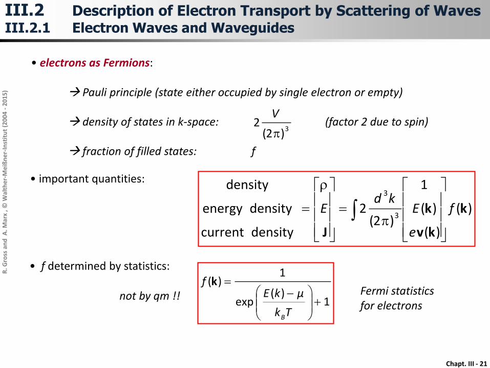
• electrons as Fermions:
Pauli principle (state either occupied by single electron or empty)
density of states in k-space: (factor 2 due to spin)
fraction of filled states: f
3)2(2
p
V
)(
)(
)(
1
)2(2
density current
density energy
density
3
3
k
kv
k
J
f
e
Ekd
E
p
1)(
exp
1)(
Tk
µkEf
B
knot by qm !!
• important quantities:
• f determined by statistics:
III.2 Description of Electron Transport by Scattering of WavesIII.2.1 Electron Waves and Waveguides
Fermi statisticsfor electrons

Chapt. III - 22
R. G
ross
and
A. M
arx
, © W
alth
er-
Me
ißn
er-
Inst
itu
t (2
00
4 -
20
15
)
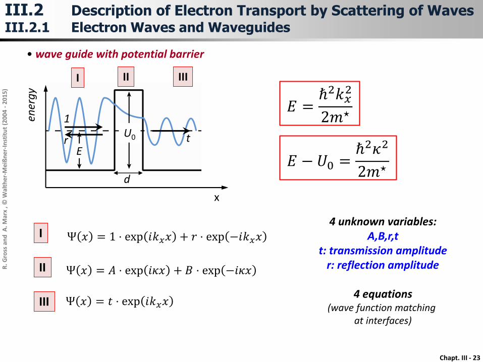
• ballistic conductor as waveguide: 1D free motion of charge carriers, e.g. in x-directionconfinement in y,z-direction
Source: Handouts Nazarov, TU Delft
III.2 Description of Electron Transport by Scattering of WavesIII.2.1 Electron Waves and Waveguides
mode index n standing waveplane wave
Ψ𝑘𝑥,𝑛 𝒓, 𝑡 = 𝜙𝑛 𝑦, 𝑧 exp[𝑖 𝑘𝑥𝑥 − 𝜔𝑡 ] 𝐸𝑛 𝑘𝑥 =ℏ2𝑘𝑥
2
2𝑚⋆ + 𝐸𝑛; 𝐸𝑛 =𝜋2ℏ2
2𝑚⋆
𝑛𝑦2
𝑎2 +𝑛𝑧
2
𝑏2
EF
2𝑚
⋆𝑎
2
𝜋2ℏ
2𝐸
𝜋𝑘𝑥/𝑎
Chapt. III - 23
R. G
ross
and
A. M
arx
, © W
alth
er-
Me
ißn
er-
Inst
itu
t (2
00
4 -
20
15
)
• wave guide with potential barrier
II
III
I4 unknown variables:
A,B,r,tt: transmission amplitude
r: reflection amplitude
4 equations(wave function matching
at interfaces)
d
ener
gy
U0 tr
1
I II III
x
III.2 Description of Electron Transport by Scattering of WavesIII.2.1 Electron Waves and Waveguides
E
𝐸 =ℏ2𝑘𝑥
2
2𝑚⋆
𝐸 − 𝑈0 =ℏ2𝜅2
2𝑚⋆
Ψ 𝑥 = 1 ⋅ exp 𝑖𝑘𝑥𝑥 + 𝑟 ⋅ exp −𝑖𝑘𝑥𝑥
Ψ 𝑥 = 𝐴 ⋅ exp 𝑖𝜅𝑥 + 𝐵 ⋅ exp −𝑖𝜅𝑥
Ψ 𝑥 = 𝑡 ⋅ exp 𝑖𝑘𝑥𝑥

Chapt. III - 24
R. G
ross
and
A. M
arx
, © W
alth
er-
Me
ißn
er-
Inst
itu
t (2
00
4 -
20
15
)
• wave guide with potential barrier example: rectangular barrier
thickbarrier
thinbarrier
E / U0
T
classical
resulttransmission probability/coefficient:
III.2 Description of Electron Transport by Scattering of WavesIII.2.1 Electron Waves and Waveguides
𝑇 𝐸 ≡ 𝑡2 =1
1 +𝑘𝑥
2 − 𝜅2
2𝑘𝑥𝜅
2
sinh2 𝜅𝑑
for 𝜅𝑑 ≫ 1:sinh2(𝜅𝑑) = exp 𝜅𝑑 − exp −𝜅𝑑 2 ≃ exp 2𝜅𝑑

Chapt. III - 28
R. G
ross
and
A. M
arx
, © W
alth
er-
Me
ißn
er-
Inst
itu
t (2
00
4 -
20
15
)
• modelling of nanostructures as complex waveguides:
transport channels + potential barrier
rese
rvo
ir
rese
rvo
ir
Tn
scattering region
ideal waveguides
sufficient to describe transport !!
examples:(i) adiabatic quantum transport(ii) quantum point contact
• description of transport by a set of transmission coefficients Tn
III.2 Description of Electron Transport by Scattering of WavesIII.2.1 Electron Waves and Waveguides

Chapt. III - 29
R. G
ross
and
A. M
arx
, © W
alth
er-
Me
ißn
er-
Inst
itu
t (2
00
4 -
20
15
)
• example: adiabatic quantum transport constriction as a potential barrier
a = const
a = a(x)
y
x
3 open channelsT = 1
x
E n(x
)
E
closed channelsT = 0
adiabatic waveguide:variation of dimensions occurs on length scale large compared to width waveguide walls can be assumed
parallel locally
III.2 Description of Electron Transport by Scattering of WavesIII.2.1 Electron Waves and Waveguides
𝐸𝑛(𝑘𝑥, 𝑥) =ℏ2𝑘𝑥
2
2𝑚⋆ +𝜋2ℏ2
2𝑚⋆
𝑛𝑦2
𝑎2(𝑥)+
𝑛𝑧2
𝑏2(𝑥)
Chapt. III - 30
R. G
ross
and
A. M
arx
, © W
alth
er-
Me
ißn
er-
Inst
itu
t (2
00
4 -
20
15
)
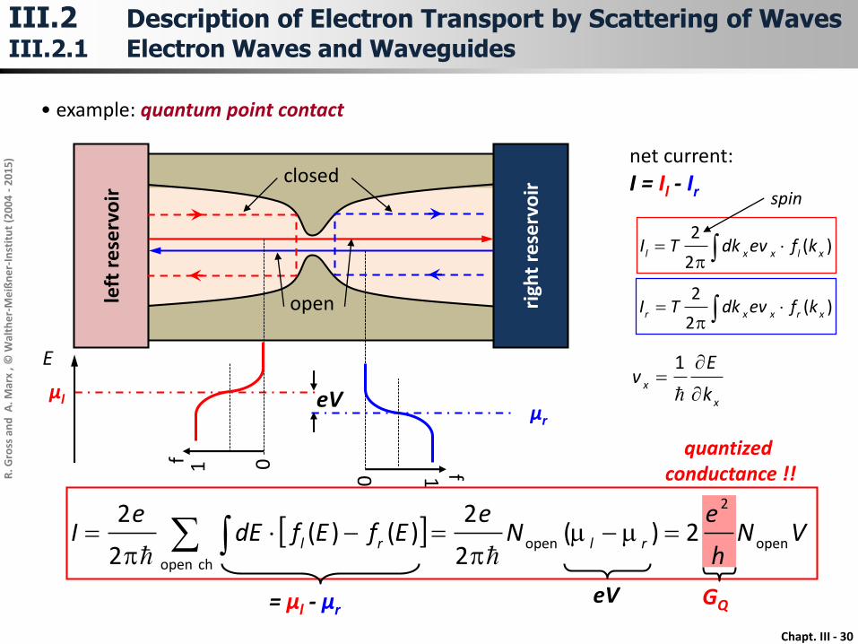
• example: quantum point contactle
ft r
ese
rvo
ir
righ
tre
serv
oir
E
µlµr
closed
open
f0 1
f 01
net current:
I = Il - Ir
p
)(2
2xlxxl kfevdkTI
p
)(2
2xrxxr kfevdkTI
x
xk
Ev
1
spin
VNh
eN
eEfEfdE
eI rlrl open
2
open
ch open
2)(2
2)()(
2
2mm
p
p
eV GQ
quantized conductance !!
= µl - µr
eV
III.2 Description of Electron Transport by Scattering of WavesIII.2.1 Electron Waves and Waveguides
Chapt. III - 31
R. G
ross
and
A. M
arx
, © W
alth
er-
Me
ißn
er-
Inst
itu
t (2
00
4 -
20
15
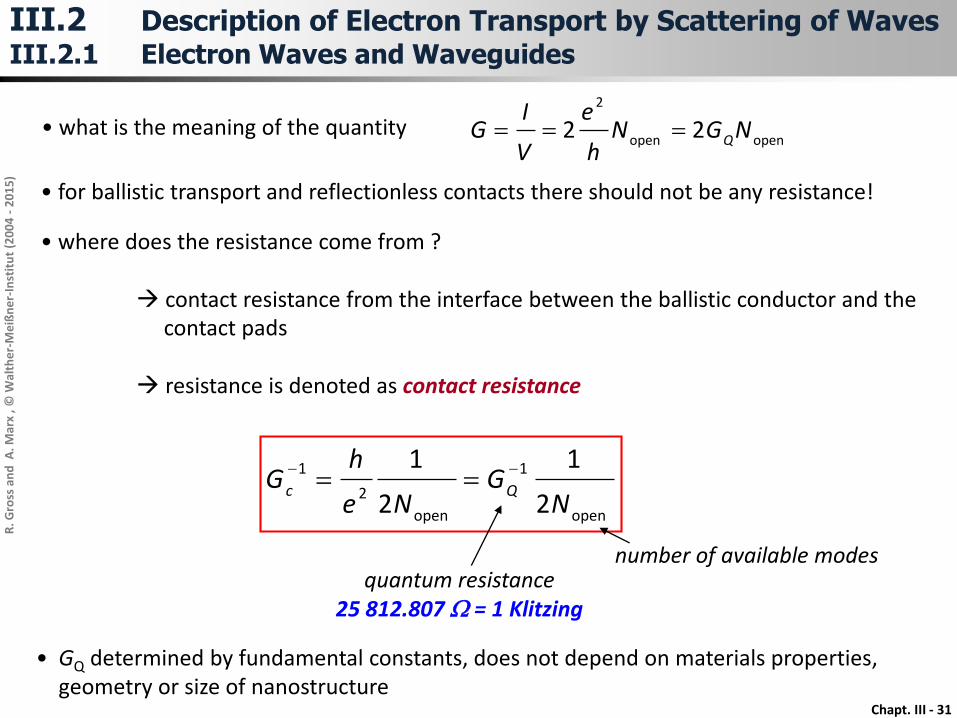
)
• what is the meaning of the quantityopenopen
2
22 NGNh
e
V
IG Q
open
1
open
2
1
2
1
2
1
NG
Ne
hG Qc
quantum resistance25 812.807 W = 1 Klitzing
number of available modes
• for ballistic transport and reflectionless contacts there should not be any resistance!
• where does the resistance come from ?
contact resistance from the interface between the ballistic conductor and thecontact pads
resistance is denoted as contact resistance
• GQ determined by fundamental constants, does not depend on materials properties, geometry or size of nanostructure
III.2 Description of Electron Transport by Scattering of WavesIII.2.1 Electron Waves and Waveguides
Chapt. III - 32
R. G
ross
and
A. M
arx
, © W
alth
er-
Me
ißn
er-
Inst
itu
t (2
00
4 -
20
15
)
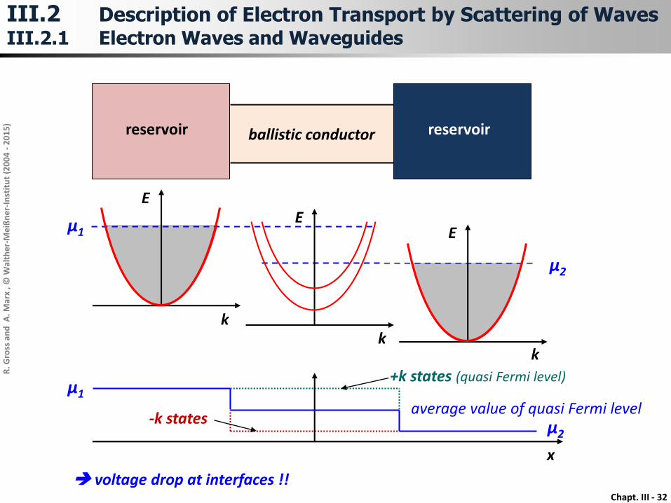
+k states (quasi Fermi level)
ballistic conductor reservoirreservoir
µ1
µ2
k
EE
E
k
k
x
µ1
µ2-k states
average value of quasi Fermi level
voltage drop at interfaces !!
III.2 Description of Electron Transport by Scattering of WavesIII.2.1 Electron Waves and Waveguides
Chapt. III - 33
R. G
ross
and
A. M
arx
, © W
alth
er-
Me
ißn
er-
Inst
itu
t (2
00
4 -
20
15
)
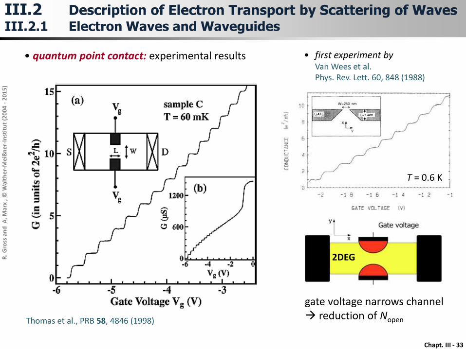
• quantum point contact: experimental results
Thomas et al., PRB 58, 4846 (1998)
gate voltage narrows channel reduction of Nopen
2DEG
• first experiment byVan Wees et al. Phys. Rev. Lett. 60, 848 (1988)
III.2 Description of Electron Transport by Scattering of WavesIII.2.1 Electron Waves and Waveguides
T = 0.6 K
Chapt. III - 34
R. G
ross
and
A. M
arx
, © W
alth
er-
Me
ißn
er-
Inst
itu
t (2
00
4 -
20
15
)
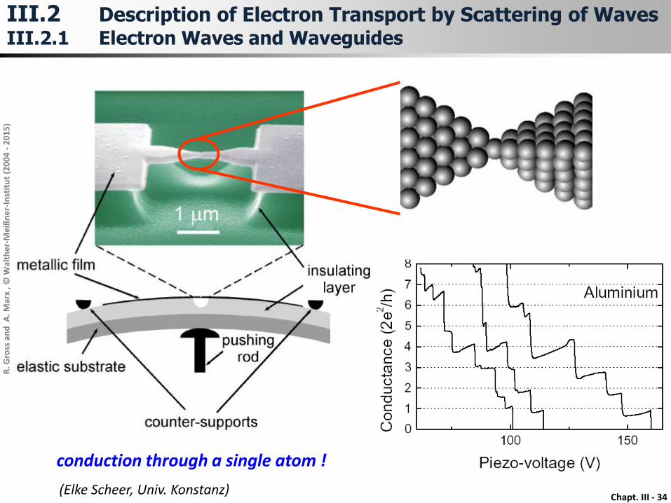
conduction through a single atom !
(Elke Scheer, Univ. Konstanz)
III.2 Description of Electron Transport by Scattering of WavesIII.2.1 Electron Waves and Waveguides
Chapt. III - 35
R. G
ross
and
A. M
arx
, © W
alth
er-
Me
ißn
er-
Inst
itu
t (2
00
4 -
20
15
)
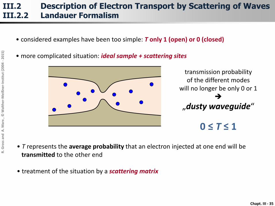
• considered examples have been too simple: T only 1 (open) or 0 (closed)
• more complicated situation: ideal sample + scattering sites
transmission probabilityof the different modes
will no longer be only 0 or 1
„dusty waveguide“
0 ≤ T ≤ 1
• T represents the average probability that an electron injected at one end will be transmitted to the other end
• treatment of the situation by a scattering matrix
III.2 Description of Electron Transport by Scattering of WavesIII.2.2 Landauer Formalism

Chapt. III - 36
R. G
ross
and
A. M
arx
, © W
alth
er-
Me
ißn
er-
Inst
itu
t (2
00
4 -
20
15
)
r12
r22
r32
1t12
t22
t32Nl Nr
Nl + Nr incoming amplitudes 𝒂𝒍, 𝒂𝒓
Nl + Nr outgoing amplitudes 𝒃𝒍, 𝒃𝒓
scattering regionleftreservoir
rightreservoir
ab s
scattering matrixscattering matrix
Nl x Nl matrix
Nr x Nr matrix
III.2 Description of Electron Transport by Scattering of WavesIII.2.2 Landauer Formalism: scattering matrix
𝑏𝑙
𝑏𝑟=
𝑠𝑙𝑙 𝑠𝑙𝑟
𝑠𝑟𝑙 𝑠𝑟𝑟
𝑎𝑙
𝑎𝑟= 𝑟 𝑡′
𝑡 𝑟′
𝑎𝑙
𝑎𝑟

Chapt. III - 37
R. G
ross
and
A. M
arx
, © W
alth
er-
Me
ißn
er-
Inst
itu
t (2
00
4 -
20
15
)
• time reversal symmetry: (sym. matrix)
• electrons do not disappear:
unitary matrix
III.2 Description of Electron Transport by Scattering of WavesIII.2.2 Landauer Formalism: scattering matrix
𝑅𝑛 = 𝑟† 𝑟𝑛𝑛
𝑇𝑛 = 𝑡† 𝑡𝑛𝑛
conjugate transposeof 𝑠
Chapt. III - 38
R. G
ross
and
A. M
arx
, © W
alth
er-
Me
ißn
er-
Inst
itu
t (2
00
4 -
20
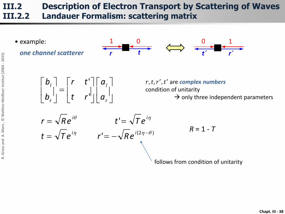
15
) r t
1 0 0 1
r´t´one channel scatterer
r
l
r
l
a
a
rt
tr
b
b
'
'
'
'
)2(
i
i
i
i
eRr
eTt
eTt
eRrR = 1 - T
III.2 Description of Electron Transport by Scattering of WavesIII.2.2 Landauer Formalism: scattering matrix
• example:
𝑟, 𝑡, 𝑟′, 𝑡′ are complex numberscondition of unitarity
only three independent parameters
follows from condition of unitarity

Chapt. III - 39
R. G
ross
and
A. M
arx
, © W
alth
er-
Me
ißn
er-
Inst
itu
t (2
00
4 -
20
15
)
𝑟⋆ 𝑡′⋆
𝑡⋆ 𝑟′⋆⋅ 𝑟 𝑡
𝑡′ 𝑟′ =𝑟 2 + 𝑡′ 2 𝑟⋆𝑡 + 𝑡′⋆𝑟′
𝑡⋆𝑟 + 𝑟′⋆𝑡′ 𝑡 2 + 𝑟′ 2= 1
• condition of unitarity: 𝑆† 𝑆 = 1= 0
= 0
III.2 Description of Electron Transport by Scattering of WavesIII.2.2 Landauer Formalism: scattering matrix
𝑟⋆𝑡 + 𝑡′⋆𝑟′ = 0
𝑅𝑒−𝑖𝜃 𝑇𝑒𝑖𝜂 − 𝑇𝑒−𝑖𝜂 𝑅𝑒𝑖 2𝜂−𝜃 =
𝑇 𝑅𝑒−𝑖 𝜃−𝜂 − 𝑇 𝑅 𝑒−𝑖 𝜃−𝜂 = 0 !!
𝑡⋆𝑟 + 𝑟′⋆𝑡′ = 0
𝑇𝑒−𝑖𝜂 ⋅ 𝑅𝑒𝑖𝜃 − 𝑅𝑒−𝑖 2𝜂−𝜃 ⋅ 𝑇𝑒𝑖𝜂 =
𝑇 𝑅𝑒𝑖 𝜃−𝜂 − 𝑇 𝑅 𝑒𝑖 𝜃−𝜂 = 0 !!
(i)
(ii)
Chapt. III - 40
R. G
ross
and
A. M
arx
, © W
alth
er-
Me
ißn
er-
Inst
itu
t (2
00
4 -
20
15
)
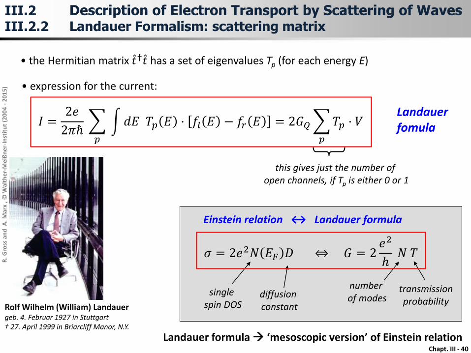
• the Hermitian matrix 𝑡† 𝑡 has a set of eigenvalues Tp (for each energy E)
this gives just the number of open channels, if Tp is either 0 or 1
Landauerfomula
Rolf Wilhelm (William) Landauergeb. 4. Februar 1927 in Stuttgart† 27. April 1999 in Briarcliff Manor, N.Y.
Einstein relation ↔ Landauer formula
singlespin DOS
diffusion constant
number of modes
transmissionprobability
• expression for the current:
Landauer formula ‘mesoscopic version’ of Einstein relation
III.2 Description of Electron Transport by Scattering of WavesIII.2.2 Landauer Formalism: scattering matrix
𝐼 =2𝑒
2𝜋ℏ
𝑝
.𝑛
. 𝑑𝐸 𝑇𝑝 𝐸 ⋅ 𝑓𝑙 𝐸 − 𝑓𝑟 𝐸 = 2𝐺𝑄
𝑝
𝑛
𝑇𝑝 ⋅ 𝑉
𝜎 = 2𝑒2𝑁 𝐸𝐹 𝐷 ⇔ 𝐺 = 2𝑒2
ℎ𝑁 𝑇
Chapt. III - 41
R. G
ross
and
A. M
arx
, © W
alth
er-
Me
ißn
er-
Inst
itu
t (2
00
4 -
20
15
)
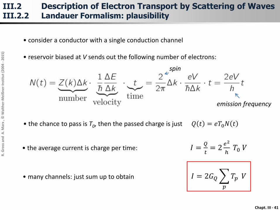
• consider a conductor with a single conduction channel
• reservoir biased at V sends out the following number of electrons:
spin
• the chance to pass is T0, then the passed charge is just 𝑄 𝑡 = 𝑒𝑇0𝑁 𝑡
• the average current is charge per time: 𝐼 =𝑄
𝑡= 2
𝑒2
ℎ𝑇0 𝑉
• many channels: just sum up to obtain
III.2 Description of Electron Transport by Scattering of WavesIII.2.2 Landauer Formalism: plausibility
emission frequency
𝐼 = 2𝐺𝑄
𝑝
𝑛
𝑇𝑝 𝑉

Chapt. III - 42
R. G
ross
and
A. M
arx
, © W
alth
er-
Me
ißn
er-
Inst
itu
t (2
00
4 -
20
15
) • restrictions:
only elastic scattering (electrons pass the conductor at constant energy) no interactions between electrons
• limitations:
low temperatures and low voltages short conductors (shorter then inelastic scattering length)
III.2 Description of Electron Transport by Scattering of WavesIII.2.2 Landauer Formalism: limitations and restrictions

Chapt. III - 43
R. G
ross
and
A. M
arx
, © W
alth
er-
Me
ißn
er-
Inst
itu
t (2
00
4 -
20
15
)
• so far discussion of two-terminal systems, extension to multi-terminal conductors?
V1
V2
V3
I2I1
I3
reservoirideal
conductor
gate
scattering region
how to express currents in terms of voltages using the Landauer formalism ?
III.2 Description of Electron Transport by Scattering of WavesIII.2.2 Additional Topic: Multi-terminal conductors

Chapt. III - 44
R. G
ross
and
A. M
arx
, © W
alth
er-
Me
ißn
er-
Inst
itu
t (2
00
4 -
20
15
)
V1
V2
V3
I2
I1
I3
4
• conduction matrix Gkl
• properties of conduction matrix:
current conservation:
no current, if potential is shifted by the same amount in all leads
l
l
klk VGI
0 0 k
kl
k
k GI
0l
klG
III.2 Description of Electron Transport by Scattering of WavesIII.2.2 Additional Topic: Multi-terminal conductors

Chapt. III - 45
R. G
ross
and
A. M
arx
, © W
alth
er-
Me
ißn
er-
Inst
itu
t (2
00
4 -
20
15
) • simplest case: two-terminal conductor
• the conduction matrix only has a single independent element:
V1 V2
I1 I2
2
1
2
1
V
V
GG
GG
I
I
III.2 Description of Electron Transport by Scattering of WavesIII.2.2 Additional Topic: Multi-terminal conductors

Chapt. III - 46
R. G
ross
and
A. M
arx
, © W
alth
er-
Me
ißn
er-
Inst
itu
t (2
00
4 -
20
15
) • scattering matrix for multi-terminal conductors
• number of modes: N = N1+N2+N3+ .... scattering matrix is NxN matrix
• meaning of Sbm,an: propagation amplitude
from terminal a, transport channel n, to the terminal b, transport channel m
• transmission probability:
s11,12
s12,12
s13,12
1N1
abab
ba
ab
N
n
mn
N
m
N
n
nm
N
m
sTT1
2
,
111
III.2 Description of Electron Transport by Scattering of WavesIII.2.2 Additional Topic: Multi-terminal conductors

Chapt. III - 47
R. G
ross
and
A. M
arx
, © W
alth
er-
Me
ißn
er-
Inst
itu
t (2
00
4 -
20
15
)
• properties of scattering matrix:
reflection back from a: San,am
transmission from b to a: San,bm
• current conservation requires
• time reversal symmetry:
(unitary matrix)
a
bbaa
n
lmmnln ss ,
*
,
)()( ,, BsBs nmmn abba
III.2 Description of Electron Transport by Scattering of WavesIII.2.2 Additional Topic: Multi-terminal conductors
Chapt. III - 48
R. G
ross
and
A. M
arx
, © W
alth
er-
Me
ißn
er-
Inst
itu
t (2
00
4 -
20
15
)
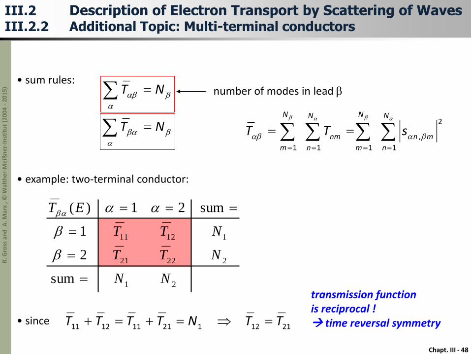
• sum rules:
• example: two-terminal conductor:
• since
b
a
ab NT
b
a
ba NT
number of modes in lead b
21
22221
11211
sum
2
1
sum21)(
NN
NTT
NTT
ET
b
b
aaba
2112121111211 TTNTTTT
transmission functionis reciprocal ! time reversal symmetry
abab
baab
N
n
mn
N
m
N
n
nm
N
m
sTT1
2
,
111
III.2 Description of Electron Transport by Scattering of WavesIII.2.2 Additional Topic: Multi-terminal conductors

Chapt. III - 49
R. G
ross
and
A. M
arx
, © W
alth
er-
Me
ißn
er-
Inst
itu
t (2
00
4 -
20
15
)
• multi-terminal expression of Landauer formula relates currents to voltages viaa scattering matrix
• probability for transmission from a to b:
• plausibility check:
current conservation is satisfied (follows from unitarity) no current is flowing in equilibrium, same voltage at all terminals
(follows also from unitarity)
trace includes allpossible transport channels
ab
ababab ssT ˆˆ Tr
b
b
aba )( EfTdE
e
GI Q
III.2 Description of Electron Transport by Scattering of WavesIII.2.2 Additional Topic: Multi-terminal conductors
Chapt. III - 50
R. G
ross
and
A. M
arx
, © W
alth
er-
Me
ißn
er-
Inst
itu
t (2
00
4 -
20
15
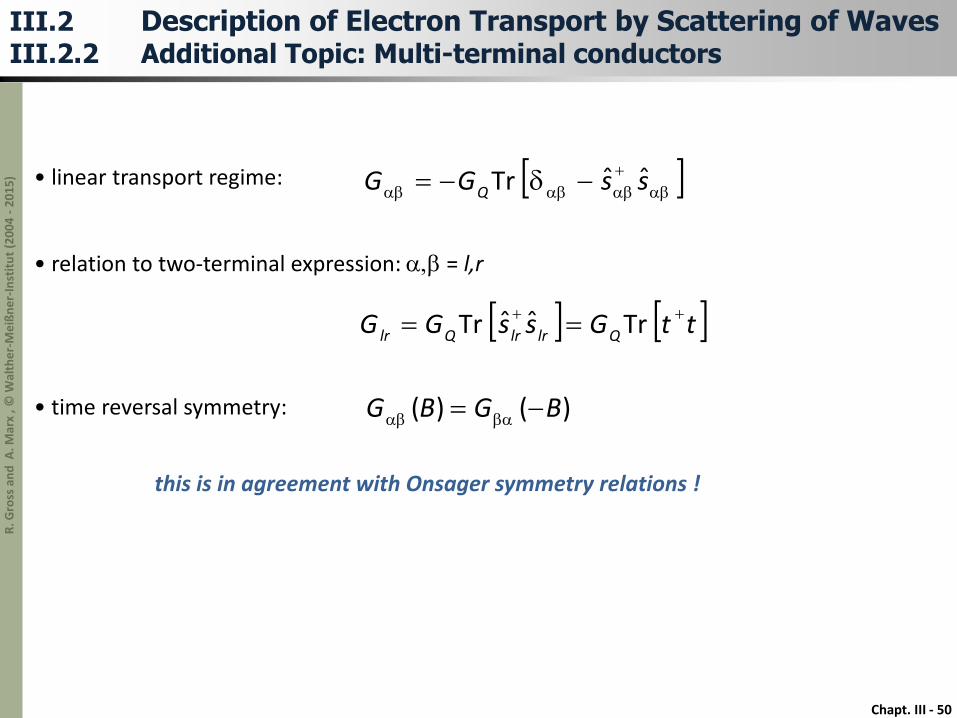
) • linear transport regime:
• relation to two-terminal expression: a,b = l,r
• time reversal symmetry:
ab
ababab ssGG Q
ˆˆ Tr
ttGssGG QlrlrQlr
Trˆˆ Tr
)()( BGBG baab
this is in agreement with Onsager symmetry relations !
III.2 Description of Electron Transport by Scattering of WavesIII.2.2 Additional Topic: Multi-terminal conductors

Chapt. III - 51
R. G
ross
and
A. M
arx
, © W
alth
er-
Me
ißn
er-
Inst
itu
t (2
00
4 -
20
15
) • three-terminal scattering element:
• scattering matrix:
• conductance matrix:
• example: V1 = V2 = V; V3 = 0
1
2
3
02/12/1
2/12/12/1
2/12/12/1
ˆBSs
ab
12/12/1
2/14/34/1
2/14/14/3
QGG
GQV
GQV/2
GQV/2
ideal beam splitter
III.2 Description of Electron Transport by Scattering of WavesIII.2.2 Additional Topic: Multi-terminal conductors
Chapt. III - 52
R. G
ross
and
A. M
arx
, © W
alth
er-
Me
ißn
er-
Inst
itu
t (2
00
4 -
20
15
)
Contents:
III.1 IntroductionIII.1.1 General RemarksIII.1.2 Mesoscopic SystemsIII.1.3 Characteristic Length ScalesIII.1.4 Characteristic Energy ScalesIII.1.5 Transport Regimes
III.2 Description of Electron Transport by Scattering of WavesIII.2.1 Electron Waves and WaveguidesIII.2.2 Landauer FormalismIII.2.3 Multi-terminal Conductors
III.3 Quantum Interference EffectsIII.3.1 Double Slit ExperimentIII.3.2 Two Barriers – Resonant TunnelingIII.3.3 Aharonov-Bohm EffectIII.3.4 Weak LocalizationIII.3.5 Universal Conductance Fluctuations
III.4 From Quantum Mechanics to Ohm‘s Law
III.5 Coulomb Blockade
III.3 Quantum Interference Effects

Chapt. III - 53
R. G
ross
and
A. M
arx
, © W
alth
er-
Me
ißn
er-
Inst
itu
t (2
00
4 -
20
15
)
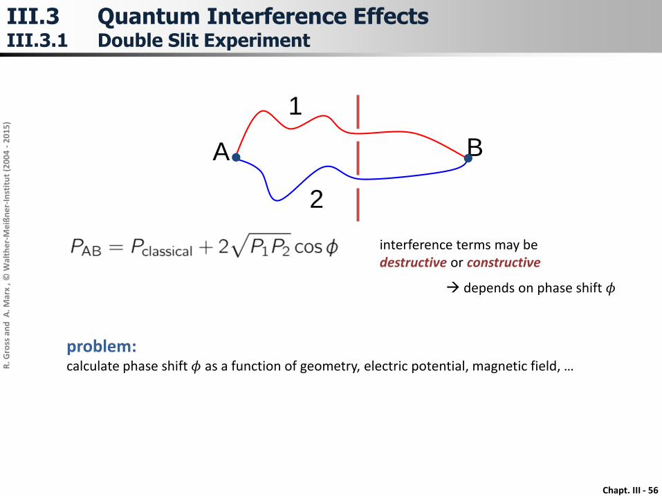
coherent charge carriers 𝐿𝜙 > 𝐿
low temperatures ( 𝐿𝜙 gets large), nanoscale samples (L gets small)
interference of multiply scattered charge carriers
corrections to the classical conductance
III.3 Quantum Interference EffectsIII.3.1 Double Slit Experiment
• macroscopic and mesoscopic samples:
weak localization (WL)
• mesoscopic samples:
Aharonov-Bohm (AB) oscillations
Universal Conductance Fluctuations (UCF)
Chapt. III - 54
R. G
ross
and
A. M
arx
, © W
alth
er-
Me
ißn
er-
Inst
itu
t (2
00
4 -
20
15
)
III.3 Quantum Interference EffectsIII.3.1 Revision: Characteristic Length Scales (see III.1.3)
elastic impurity scattering: 𝜏𝜑 → 0 or 𝛼𝜑 → 0
electron-phonon scattering: 𝜏𝜑 ≈ 𝜏𝑒−𝑝ℎ ??
electron-electron scattering: 𝜏𝜑 ≈ 𝜏𝑒−𝑒 ??
electron-impuritiy scattering
• electron wavelength: 𝝀𝑭 =𝒉
𝟐𝒎⋆𝑬𝑭=
𝟐𝝅
𝟑𝝅𝟐𝒏𝟏/𝟑 (Fermi wavelength)
collision time
effectiveness ofcollision: 0 < am < 1
• mean free path: ℓ = 𝒗𝑭 ⋅ 𝝉𝒎 𝝉𝒎−𝟏 = 𝝉𝒄
−𝟏 ⋅ 𝜶𝒎
(with internal degree of freedom, e.g. spin)
• phase relaxation length: 𝑳𝝋 = 𝒗𝑭𝝉𝝋 𝝉𝝋−𝟏 = 𝝉𝒄
−𝟏 ⋅ 𝜶𝝋 effectiveness ofcollision in destroyingphase coherence: 0 < aj < 1
ballistic
diffusive 𝑳𝝋 = 𝑫𝝉𝝋 =𝟏
𝟑𝒗𝑭
𝟐𝝉𝒎𝝉𝝋

Chapt. III - 55
R. G
ross
and
A. M
arx
, © W
alth
er-
Me
ißn
er-
Inst
itu
t (2
00
4 -
20
15
)
A B
1
2
• basic quantum mechanics: double slit experiment
• probability of propagation from point A to point B:
classical interference term:quantum mechanical
P1 P2
III.3 Quantum Interference EffectsIII.3.1 Double Slit Experiment
Chapt. III - 56
R. G
ross
and
A. M
arx
, © W
alth
er-
Me
ißn
er-
Inst
itu
t (2
00
4 -
20
15
)
A B
1
2
interference terms may be destructive or constructive
depends on phase shift 𝜙
III.3 Quantum Interference EffectsIII.3.1 Double Slit Experiment
problem: calculate phase shift 𝜙 as a function of geometry, electric potential, magnetic field, …
Chapt. III - 57
R. G
ross
and
A. M
arx
, © W
alth
er-
Me
ißn
er-
Inst
itu
t (2
00
4 -
20
15
)
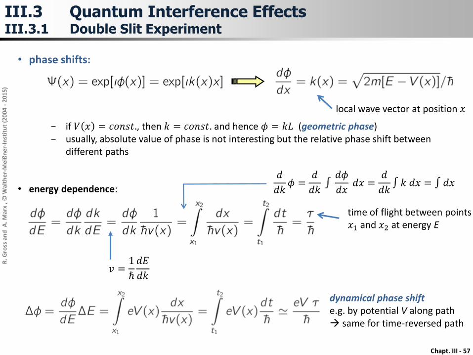
• phase shifts:
• energy dependence:
dynamical phase shift e.g. by potential V along path same for time-reversed path
time of flight between points𝑥1 and 𝑥2 at energy E
III.3 Quantum Interference EffectsIII.3.1 Double Slit Experiment
local wave vector at position 𝑥
− if 𝑉 𝑥 = 𝑐𝑜𝑛𝑠𝑡., then 𝑘 = 𝑐𝑜𝑛𝑠𝑡. and hence 𝜙 = 𝑘𝐿 (geometric phase)− usually, absolute value of phase is not interesting but the relative phase shift between
different paths
𝑣 =1
ℏ
𝑑𝐸
𝑑𝑘
𝑑
𝑑𝑘𝜙 =
𝑑
𝑑𝑘∫
𝑑𝜙
𝑑𝑥𝑑𝑥 =
𝑑
𝑑𝑘∫ 𝑘 𝑑𝑥 = ∫ 𝑑𝑥

Chapt. III - 58
R. G
ross
and
A. M
arx
, © W
alth
er-
Me
ißn
er-
Inst
itu
t (2
00
4 -
20
15
)
III.3 Quantum Interference EffectsIII.3.1 Double Slit Experiment
• magnetic field dependence:
A B
1
2
Fcanonical momentum: p = mv + qA
phase shift accumulated along the trajectory due to magnetic field:
phase shift along closed path (electron returns to the same point):
(„normal“ flux quantum)
x2 x2
(q = - e)
(in superconductors we have 𝑞𝑠 = −2𝑒and therefore Φ0 = ℎ/2𝑒)
results in phase shift 𝜙𝑚𝑎𝑔
Stokes theorem
Chapt. III - 59
R. G
ross
and
A. M
arx
, © W
alth
er-
Me
ißn
er-
Inst
itu
t (2
00
4 -
20
15
)
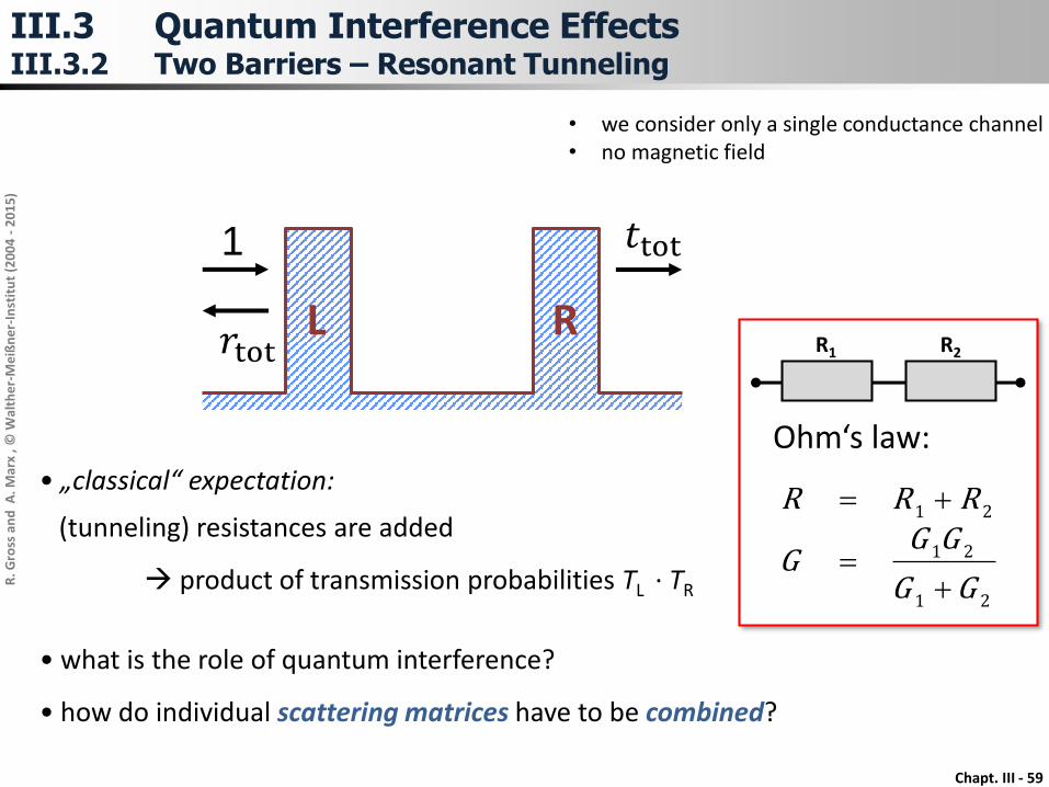
1
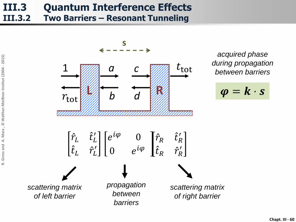
𝑟tot
𝑡tot
• „classical“ expectation:
(tunneling) resistances are added
product of transmission probabilities TL ∙ TR
L R
• we consider only a single conductance channel• no magnetic field
III.3 Quantum Interference EffectsIII.3.2 Two Barriers – Resonant Tunneling
21
21
21
GG
GGG
RRR
Ohm‘s law:
R1 R2
• what is the role of quantum interference?
• how do individual scattering matrices have to be combined?
Chapt. III - 60
R. G
ross
and
A. M
arx
, © W
alth
er-
Me
ißn
er-
Inst
itu
t (2
00
4 -
20
15
)
1
L R
a c
b d
scattering matrix
of left barrier
scattering matrix
of right barrier
propagation
between
barriers
sacquired phase
during propagation
between barriers
III.3 Quantum Interference EffectsIII.3.2 Two Barriers – Resonant Tunneling
𝑟tot
𝑡tot
𝝋 = 𝒌 ⋅ 𝒔
𝑟𝐿 𝑡𝐿′
𝑡𝐿 𝑟𝐿′
𝑟𝑅 𝑡𝑅′
𝑡𝑅 𝑟𝑅′
𝑒𝑖𝜑 0𝑜
0𝑜 𝑒𝑖𝜑𝑜

Chapt. III - 61
R. G
ross
and
A. M
arx
, © W
alth
er-
Me
ißn
er-
Inst
itu
t (2
00
4 -
20
15
)
1
L R
a aeiφ
deiφ d
outgoing modes incoming modes
outgoing modes incoming modes
III.3 Quantum Interference EffectsIII.3.2 Two Barriers – Resonant Tunneling
𝑟tot
𝑡tot
s
𝑟𝑡𝑜𝑡
𝑎0=
𝑟𝐿 𝑡𝐿′
𝑡𝐿 𝑟𝐿′
1𝑑𝑒𝑖𝜑
𝑑𝑡𝑡𝑜𝑡0
= 𝑟𝑅 𝑡𝑅
′
𝑡𝑅 𝑟𝑅′
𝑎𝑒𝑖𝜑
0

Chapt. III - 62
R. G
ross
and
A. M
arx
, © W
alth
er-
Me
ißn
er-
Inst
itu
t (2
00
4 -
20
15
)
ji
RL ett
j i
RLRL errtt 3
RLTT
RLRL RRTT
process amplitude probability
… … …
j
i
RL
RLtot
err
ttt
21 RL
RLcl
RR
TTT
1
sum of all amplitudes: sum of all probabilities:
coherent incoherent
Ttot = |ttot|²
path can be viewedas Feynman path
III.3 Quantum Interference EffectsIII.3.2 Two Barriers – Resonant Tunneling
cos21
2
tot
RLRL
RL
RRRR
TTt

Chapt. III - 63
R. G
ross
and
A. M
arx
, © W
alth
er-
Me
ißn
er-
Inst
itu
t (2
00
4 -
20
15
) 1
rtot
ttot
L R
a aeiφ
deiφ d
j
i
RL
RLtot
err
ttt
21
cos21)(
2
tot
RLRL
RL
RRRR
TTtET
what is the relation to the double slit experiment?
phase accumulatedduring the round trip
𝜒 = 2𝜑 = 2𝑘𝑠
III.3 Quantum Interference EffectsIII.3.2 Two Barriers – Resonant Tunneling
s
Chapt. III - 64
R. G
ross
and
A. M
arx
, © W
alth
er-
Me
ißn
er-
Inst
itu
t (2
00
4 -
20
15
)
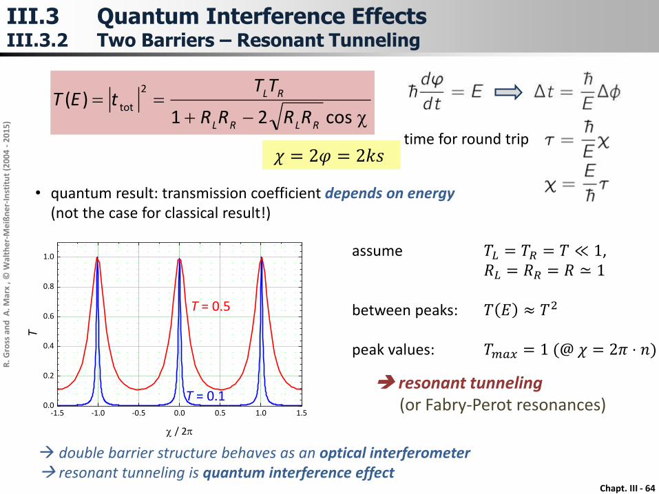
cos21)(
2
tot
RLRL
RL
RRRR
TTtET
time for round trip
• quantum result: transmission coefficient depends on energy(not the case for classical result!)
assume 𝑇𝐿 = 𝑇𝑅 = 𝑇 ≪ 1, 𝑅𝐿 = 𝑅𝑅 = 𝑅 ≃ 1
between peaks: 𝑇 𝐸 ≈ 𝑇2
peak values: 𝑇𝑚𝑎𝑥 = 1 (@ 𝜒 = 2𝜋 ⋅ 𝑛)
resonant tunneling(or Fabry-Perot resonances)
double barrier structure behaves as an optical interferometer resonant tunneling is quantum interference effect
𝜒 = 2𝜑 = 2𝑘𝑠
-1.5 -1.0 -0.5 0.0 0.5 1.0 1.50.0
0.2
0.4
0.6
0.8
1.0
T
/ 2p
T = 0.5
T = 0.1
III.3 Quantum Interference EffectsIII.3.2 Two Barriers – Resonant Tunneling

Chapt. III - 65
R. G
ross
and
A. M
arx
, © W
alth
er-
Me
ißn
er-
Inst
itu
t (2
00
4 -
20
15
)
III.3 Quantum Interference EffectsIII.3.2 Two Barriers – Resonant Tunneling
-1.5 -1.0 -0.5 0.0 0.5 1.0 1.50.0
0.2
0.4
0.6
0.8
1.0
T
/ 2p
T = 0.5
T = 0.1
cos21)(
2
tot
RLRL
RL
RRRR
TTtET
(i) 𝜒 = 0:
(ii) 𝜒 = 𝜋:
𝑇𝐿,𝑅 ≪ 1, 𝑅𝐿,𝑅 → 1:
(expanding the denominator up to linear term in TL,R)
Chapt. III - 66
R. G
ross
and
A. M
arx
, © W
alth
er-
Me
ißn
er-
Inst
itu
t (2
00
4 -
20
15
)
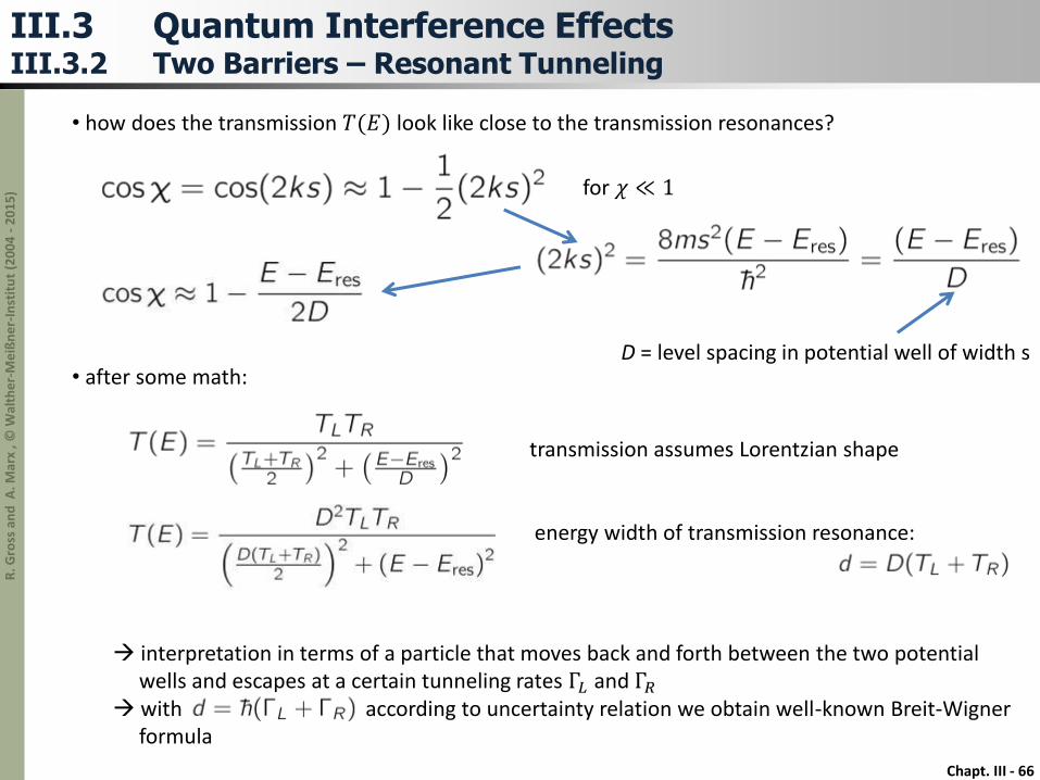
• how does the transmission 𝑇(𝐸) look like close to the transmission resonances?
D = level spacing in potential well of width s
for 𝜒 ≪ 1
• after some math:
transmission assumes Lorentzian shape
interpretation in terms of a particle that moves back and forth between the two potential wells and escapes at a certain tunneling rates Γ𝐿 and Γ𝑅
with according to uncertainty relation we obtain well-known Breit-Wigner formula
III.3 Quantum Interference EffectsIII.3.2 Two Barriers – Resonant Tunneling
energy width of transmission resonance:
Chapt. III - 67
R. G
ross
and
A. M
arx
, © W
alth
er-
Me
ißn
er-
Inst
itu
t (2
00
4 -
20
15
)
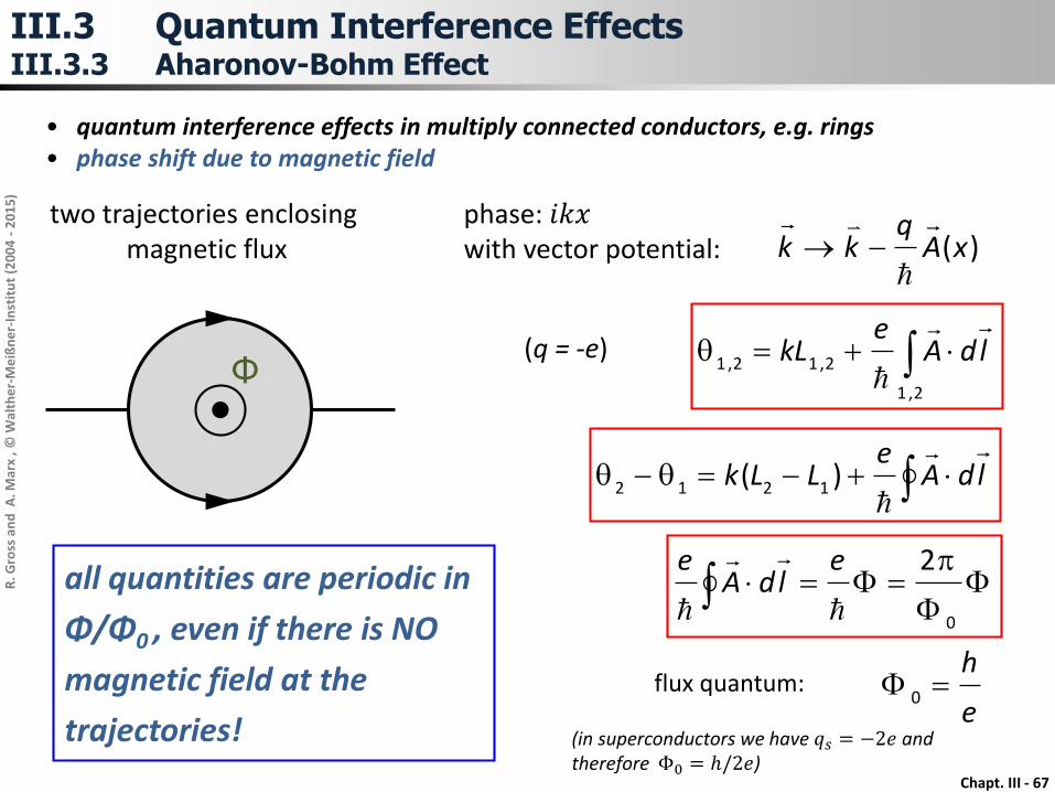
Φ
two trajectories enclosingmagnetic flux
phase: 𝑖𝑘𝑥with vector potential: )(xA
qkk
2,1
2,12,1 ldAe
kL
ldAe
LLk
)( 1212
FF
pF
0
2
eldA
e
e
hF 0
flux quantum:
all quantities are periodic in
Φ/Φ0 , even if there is NO
magnetic field at the
trajectories!
• quantum interference effects in multiply connected conductors, e.g. rings• phase shift due to magnetic field
(in superconductors we have 𝑞𝑠 = −2𝑒 andtherefore Φ0 = ℎ/2𝑒)
III.3 Quantum Interference EffectsIII.3.3 Aharonov-Bohm Effect
(q = -e)
Chapt. III - 68
R. G
ross
and
A. M
arx
, © W
alth
er-
Me
ißn
er-
Inst
itu
t (2
00
4 -
20
15
)
Φ1
r
t
b1
a1
c1
d1
b2
a2
c2
d2
1
1
1
1
1
212121
212121
21210
c
a
d
b
r
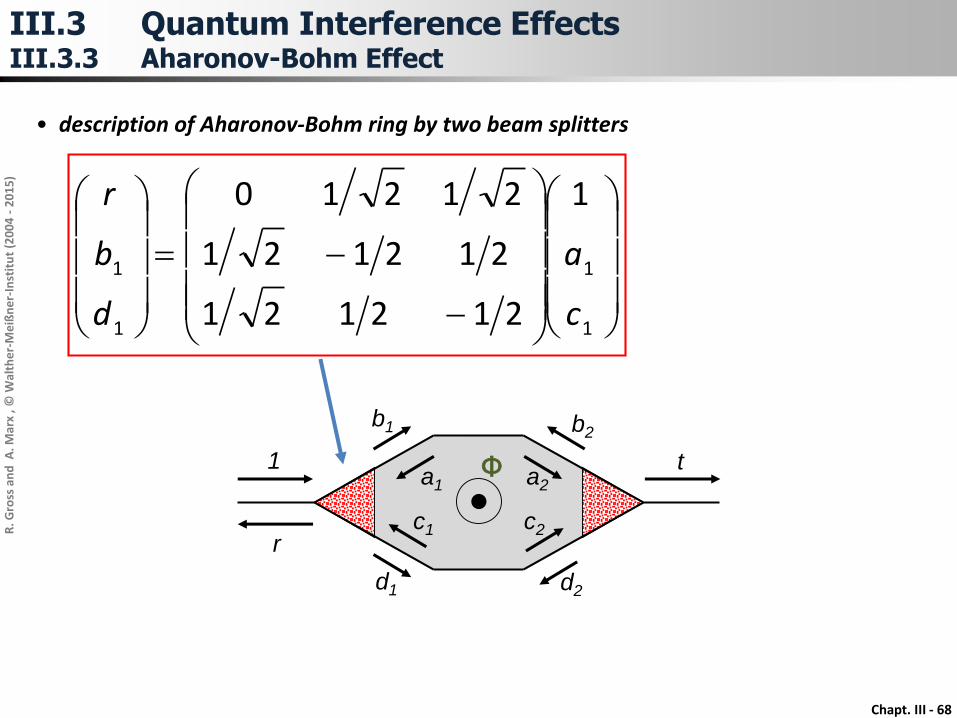
• description of Aharonov-Bohm ring by two beam splitters
III.3 Quantum Interference EffectsIII.3.3 Aharonov-Bohm Effect
Chapt. III - 69
R. G
ross
and
A. M
arx
, © W
alth
er-
Me
ißn
er-
Inst
itu
t (2
00
4 -
20
15
)
Φ1
r
t
b1
a1
c1
d1
b2
a2
c2
d2
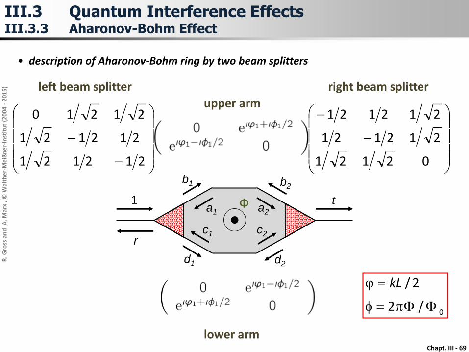
212121
212121
21210
02121
212121
212121
left beam splitter right beam splitter
upper arm
lower arm
0/2
2/
FFpf
j kL
• description of Aharonov-Bohm ring by two beam splitters
III.3 Quantum Interference EffectsIII.3.3 Aharonov-Bohm Effect
Chapt. III - 70
R. G
ross
and
A. M
arx
, © W
alth
er-
Me
ißn
er-
Inst
itu
t (2
00
4 -
20
15
)
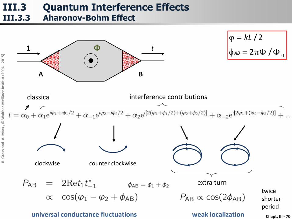
Φ1 t
classical
clockwise counter clockwise
extra turn
0/2
2/
FFpf
j
AB
kL
A B
interference contributions
twiceshorterperiod
III.3 Quantum Interference EffectsIII.3.3 Aharonov-Bohm Effect
universal conductance fluctuations weak localization
Chapt. III - 71
R. G
ross
and
A. M
arx
, © W
alth
er-
Me
ißn
er-
Inst
itu
t (2
00
4 -
20
15
)
Φ1 t
2AB
2
AB
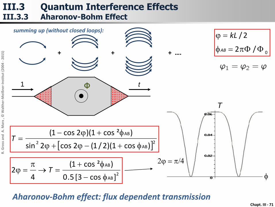
)cos1)(2/1(2cos2sin
)²cos1)(2cos1(
fjj
fjT
2AB
AB
]cos3[ 5.0
)²cos1(
42
f
f
pj T
Aharonov-Bohm effect: flux dependent transmission
f
T
2j p/4
0/2
2/
FFpf
j
AB
kLsumming up (without closed loops):
+ + + ….
III.3 Quantum Interference EffectsIII.3.3 Aharonov-Bohm Effect

Chapt. III - 72
R. G
ross
and
A. M
arx
, © W
alth
er-
Me
ißn
er-
Inst
itu
t (2
00
4 -
20
15
)
Aharonov-Bohm (AB) oscillations:
• period: h/e• amplitude: 2e2/h• one channel in Landauer model
Fourier analysis shows that there are also weak oscillations with half period
higher order interferences:Altshuler-Aronov-Spivak (AAS)oscillations
• period: h/2e• exactly same traces• constructive interference for B = 0• coherent backscattering
R. Webb et al, PRL 54, 2696 (1985)
III.3 Quantum Interference EffectsIII.3.3 Aharonov-Bohm Effect

Chapt. III - 73
R. G
ross
and
A. M
arx
, © W
alth
er-
Me
ißn
er-
Inst
itu
t (2
00
4 -
20
15
)
• AB oscillations vanish in an ensemble of small ring (phases 2𝜋Φ/Φ0 are random)• AAS oscillations survive ensemble averaging
test of ensemble averaging:• Ag loops• area 940 x 940 nm2
• width of wires 80 nm
Umbach et al, PRL 56, 386 (1986)
III.3 Quantum Interference EffectsIII.3.3 Aharonov-Bohm Effect
Chapt. III - 74
R. G
ross
and
A. M
arx
, © W
alth
er-
Me
ißn
er-
Inst
itu
t (2
00
4 -
20
15
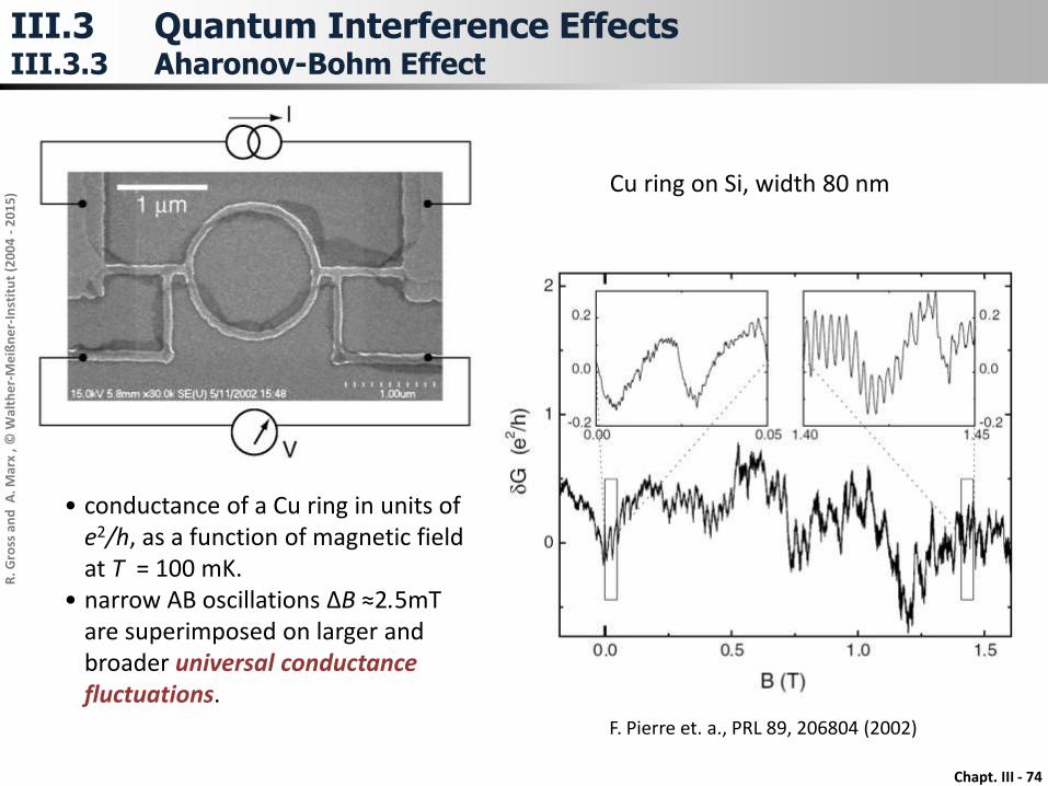
) Cu ring on Si, width 80 nm
F. Pierre et. a., PRL 89, 206804 (2002)
• conductance of a Cu ring in units ofe2/h, as a function of magnetic fieldat T = 100 mK.
• narrow AB oscillations ΔB ≈2.5mT are superimposed on larger andbroader universal conductancefluctuations.
III.3 Quantum Interference EffectsIII.3.3 Aharonov-Bohm Effect
Chapt. III - 75
R. G
ross
and
A. M
arx
, © W
alth
er-
Me
ißn
er-
Inst
itu
t (2
00
4 -
20
15
)
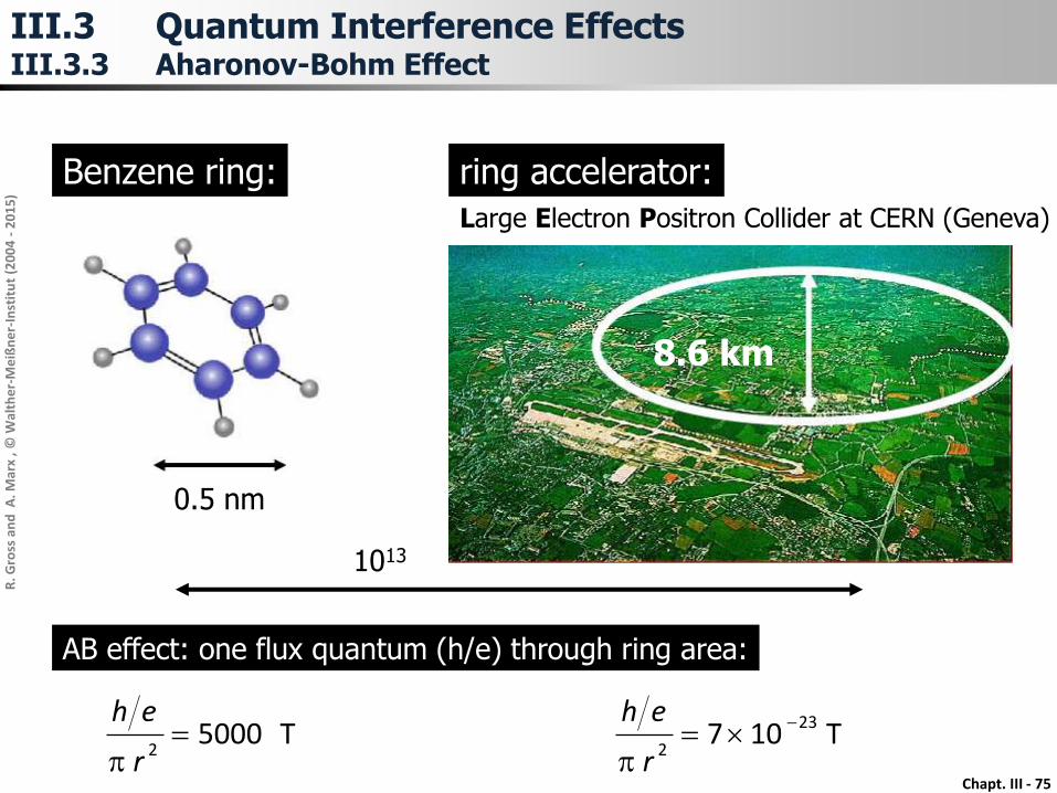
8.6 km
Benzene ring: ring accelerator:
Large Electron Positron Collider at CERN (Geneva)
0.5 nm
1013
AB effect: one flux quantum (h/e) through ring area:
T 5000 2
p r
ehT107
23
2
p r
eh
III.3 Quantum Interference EffectsIII.3.3 Aharonov-Bohm Effect
Chapt. III - 76
R. G
ross
and
A. M
arx
, © W
alth
er-
Me
ißn
er-
Inst
itu
t (2
00
4 -
20
15
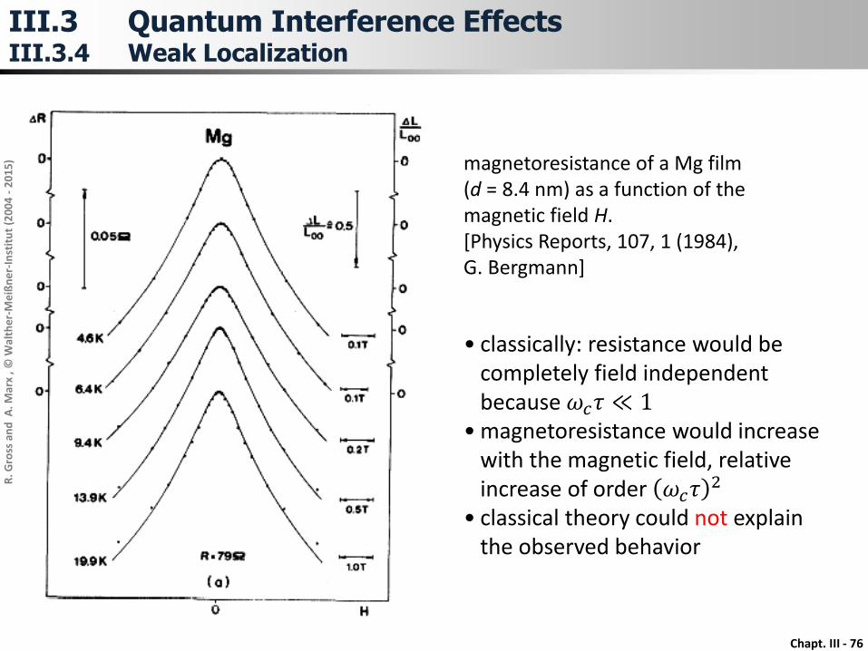
) magnetoresistance of a Mg film (d = 8.4 nm) as a function of the magnetic field H. [Physics Reports, 107, 1 (1984), G. Bergmann]
• classically: resistance would be completely field independent because 𝜔𝑐𝜏 ≪ 1
• magnetoresistance would increase with the magnetic field, relative increase of order 𝜔𝑐𝜏 2
• classical theory could not explain the observed behavior
III.3 Quantum Interference EffectsIII.3.4 Weak Localization
Chapt. III - 77
R. G
ross
and
A. M
arx
, © W
alth
er-
Me
ißn
er-
Inst
itu
t (2
00
4 -
20
15
)
Weak localization:
interference of time reversed
electron paths
III.3 Quantum Interference EffectsIII.3.4 Weak Localization
Chapt. III - 78
R. G
ross
and
A. M
arx
, © W
alth
er-
Me
ißn
er-
Inst
itu
t (2
00
4 -
20
15
)
III.3 Quantum Interference EffectsIII.3.4 Weak Localization

Chapt. III - 79
R. G
ross
and
A. M
arx
, © W
alth
er-
Me
ißn
er-
Inst
itu
t (2
00
4 -
20
15
) 2
*
1
2
2
2
1
2
21 Re2 AAAAAAPAB
classicalinterference term
quantum mechanical
P1 P2
A1
A2
special trajectories:
consider now a closed loop with 1 = 2
then the amplitude A2 is just
a time reversal of A1. Hence
2
1
2*
11
2
21 4 AAAAA
• the backscattering probability is enhanced by factor 2 !!!
• this is a predecessor of localization.
jcos||2 21 AA
A B
0cos j
does averaging overmany paths destroyinterference effects
in diffusive conductor ?
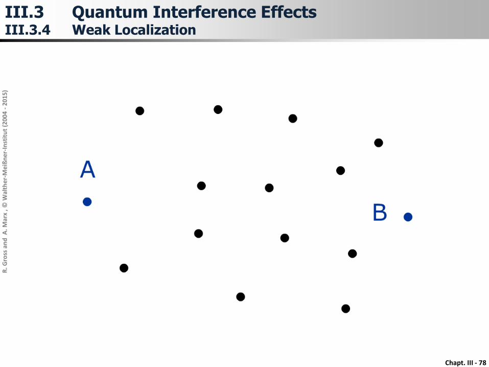
III.3 Quantum Interference EffectsIII.3.4 Weak Localization

Chapt. III - 80
R. G
ross
and
A. M
arx
, © W
alth
er-
Me
ißn
er-
Inst
itu
t (2
00
4 -
20
15
)
• magnetic field dependence of WL:
A1
A2
F
ff dsAe
AA
212
loss of constructive interference for:
0
42
12 F
pff
FBdsA
eAA
F = area of the enclosed loopB∙F = flux enclosed in the loop
characteristic field:
pff 212 AA
𝐹 ≃ 𝐿𝜙222
*f
eL
B
III.3 Quantum Interference EffectsIII.3.4 Weak Localization
calculate phase difference of
time reversed paths:

Chapt. III - 81
R. G
ross
and
A. M
arx
, © W
alth
er-
Me
ißn
er-
Inst
itu
t (2
00
4 -
20
15
)
• coherent backscattering: called the weak localization (the relative number of contributing closed loops is small)
• effect is important, since it is sensitive to weak magnetic fields:
• small fields: contributions of large rings oscillate rapidly, phase difference in small rings almost unchanged
• the larger the field, the fewer loops/rings contribute to constructive backscattering
• resistance drops to classical value for large fields, if phase shift in smallest rings is about 2p
• WL has to be distinguished from strong localization (due to strong disorder)
III.3 Quantum Interference EffectsIII.3.4 Weak Localization

Chapt. III - 82
R. G
ross
and
A. M
arx
, © W
alth
er-
Me
ißn
er-
Inst
itu
t (2
00
4 -
20
15
)
weak localizationin SiGe2-dimensionalquantum well withhole gas
• requirement: sample larger than elastic scattering length: 𝐿 > ℓ
conductivity reduced by ≈ 2e2/h for B = 0
• large B: Shubnikov de-Haas oscillations
V. Senz, PhD thesis, ETH Zürich (2002)
III.3 Quantum Interference EffectsIII.3.4 Weak Localization

Chapt. III - 83
R. G
ross
and
A. M
arx
, © W
alth
er-
Me
ißn
er-
Inst
itu
t (2
00
4 -
20
15
)
• dependence of magnitude of WL on the coherence time 𝜏𝜙 ∼ 𝐿𝜙2 /𝐷 is known:
weak localization experiments can be used to determine tf
Senz et al., PRB 61, 5082 (2000)
III.3 Quantum Interference EffectsIII.3.4 Weak Localization

Chapt. III - 84
R. G
ross
and
A. M
arx
, © W
alth
er-
Me
ißn
er-
Inst
itu
t (2
00
4 -
20
15
)
-8 -6 -4 -2 0 2 4 6 8
-0.5
0.0
0.5
1.0
1.5
200mK
B(T)
DG
(e2/h
)
800mK
fff
'
)(
'
2
2
'
pp
i
pp
p
p
p
i
pippp eAAAeAT
A
B
influence of magnetic field on conductance of simply connected conductor
F
random phase shifts position of scatters
becomes important
III.3 Quantum Interference EffectsIII.3.5 Universal Conductance Fluctuations

Chapt. III - 85
R. G
ross
and
A. M
arx
, © W
alth
er-
Me
ißn
er-
Inst
itu
t (2
00
4 -
20
15
)
• irregular conductance variations as a function of magnetic field (B), carrier
density (n), and voltage (V)
• conductance variations are symmetric with respect to B (2 probe setup)
• different in each individual sample (”magnetic fingerprint”)
• caused by irregular quantum interference
• fluctuations characterize impurity configuration
• no sample size dependence
• (border & impurity scattering)
• amplitude of conductance variations is of the order e2/h
• not noise
• theory based on ergodicity theorem
Experimental observations:
III.3 Quantum Interference EffectsIII.3.5 Universal Conductance Fluctuations

Chapt. III - 86
R. G
ross
and
A. M
arx
, © W
alth
er-
Me
ißn
er-
Inst
itu
t (2
00
4 -
20
15
)
phase shift of individual electron trajectories depends on
• magnetic field B• voltage V• Fermi energy EF (carrier density) • impurity (scatterer) configuration
consider an ensemble of macroscopically identical but microscopically different samples (different configurations of scattering centers)
variance of ensemble conductance:
2
2
42
mn
mn
mn
mn TTh
eGG
2
mnmn tT → complicated calculation
III.3 Quantum Interference EffectsIII.3.5 Universal Conductance Fluctuations
Chapt. III - 87
R. G
ross
and
A. M
arx
, © W
alth
er-
Me
ißn
er-
Inst
itu
t (2
00
4 -
20
15
)
1 2 3 4 5 6 7-0.4
-0.2
0.0
0.2
0.4
0.6
0.8
G -
<G
> (
e2/h
)
B (T)
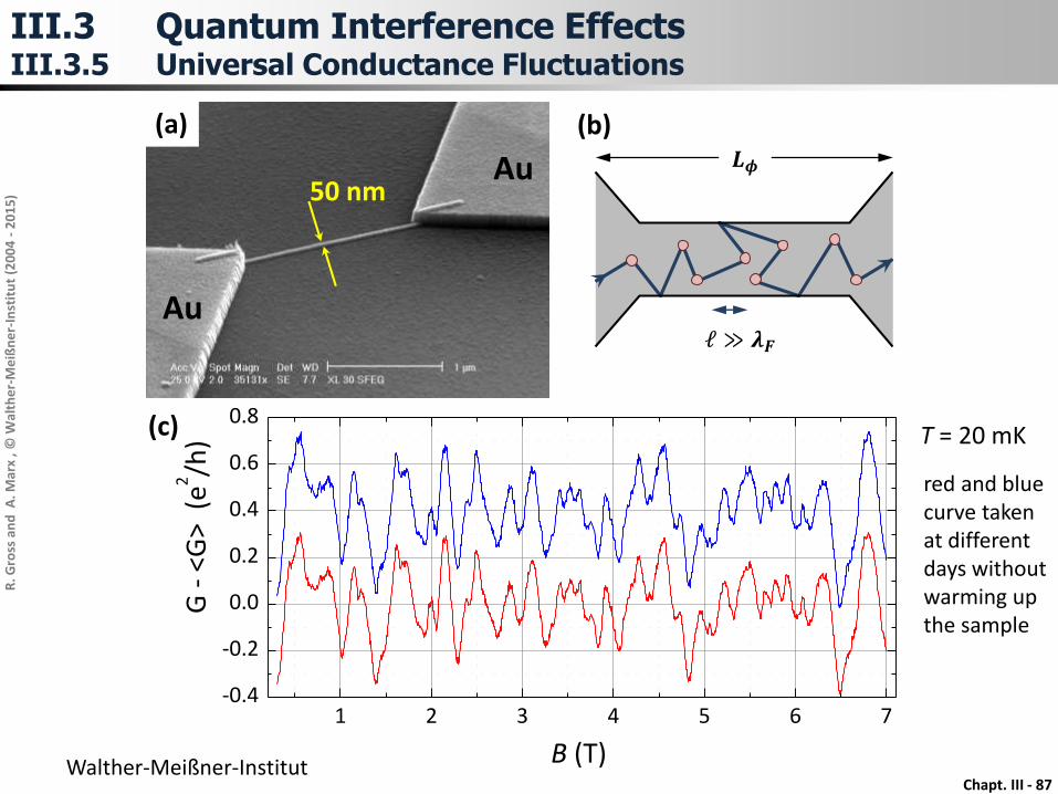
50 nm
Au
Au 𝑳𝝓
ℓ ≫ 𝝀𝑭
(a) (b)
(c)
III.3 Quantum Interference EffectsIII.3.5 Universal Conductance Fluctuations
T = 20 mK
Walther-Meißner-Institut
red and bluecurve takenat different days withoutwarming upthe sample
Chapt. III - 88
R. G
ross
and
A. M
arx
, © W
alth
er-
Me
ißn
er-
Inst
itu
t (2
00
4 -
20
15
)
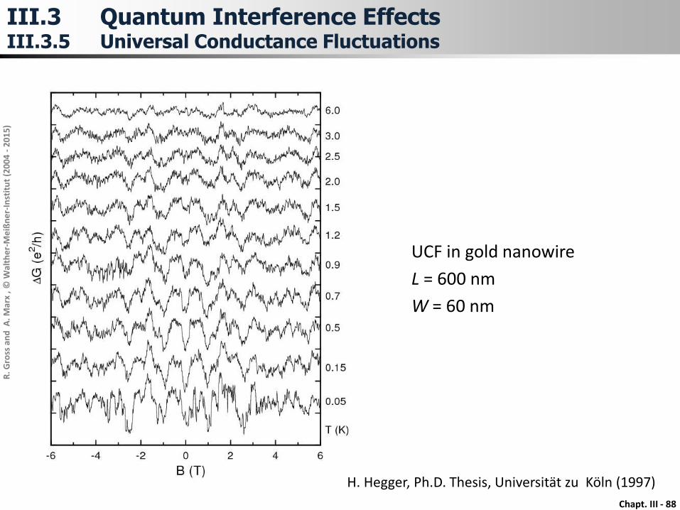
H. Hegger, Ph.D. Thesis, Universität zu Köln (1997)
UCF in gold nanowire
L = 600 nm
W = 60 nm
III.3 Quantum Interference EffectsIII.3.5 Universal Conductance Fluctuations

Chapt. III - 90
R. G
ross
and
A. M
arx
, © W
alth
er-
Me
ißn
er-
Inst
itu
t (2
00
4 -
20
15
)
data fromHeinzel (2003)
III.3 Quantum Interference EffectsIII.3.5 Universal Conductance Fluctuations

Chapt. III - 91
R. G
ross
and
A. M
arx
, © W
alth
er-
Me
ißn
er-
Inst
itu
t (2
00
4 -
20
15
)
Contents:
III.1 IntroductionIII.1.1 General RemarksIII.1.2 Mesoscopic SystemsIII.1.3 Characteristic Length ScalesIII.1.4 Characteristic Energy ScalesIII.1.5 Transport Regimes
III.2 Description of Electron Transport by Scattering of WavesIII.2.1 Electron Waves and WaveguidesIII.2.2 Landauer FormalismIII.2.3 Multi-terminal Conductors
III.3 Quantum Interference EffectsIII.3.1 Double Slit ExperimentIII.3.2 Two Barriers – Resonant TunnelingIII.3.3 Aharonov-Bohm EffectIII.3.4 Weak LocalizationIII.3.5 Universal Conductance Fluctuations
III.4 From Quantum Mechanics to Ohm‘s Law
III.5 Coulomb Blockade

Chapt. III - 92
R. G
ross
and
A. M
arx
, © W
alth
er-
Me
ißn
er-
Inst
itu
t (2
00
4 -
20
15
)
• two different points of view:
quantum transport(electron waves, scattering matrix)
classical transport(electric currents, charged particles, friction due to scattering, Ohm‘s law)
What is the bridge between these limiting cases ??
III.4 From Quantum Mechanics to Ohm‘s Law

Chapt. III - 93
R. G
ross
and
A. M
arx
, © W
alth
er-
Me
ißn
er-
Inst
itu
t (2
00
4 -
20
15
)
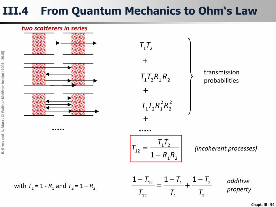
• consider two conductors with transmission probabilities T1 and T2 connected in series
T1R1 T2R2
• what is the transmission probability T12 ?
• problem: if we assume T12 = T1 T2 , then we do not take into account multiple reflections
to obtain the correct result we have to add the probabilities of multiplyreflected paths
III.4 From Quantum Mechanics to Ohm‘s Law
• If T12 = T1 T2 , then for a chain of scatterers we would expect the transmissionprobability to drop exponentially with the length of the chain:
no Ohm‘s law
)/exp()( 0LLLT ex1 ex2 = ex1+x2
Chapt. III - 94
R. G
ross
and
A. M
arx
, © W
alth
er-
Me
ißn
er-
Inst
itu
t (2
00
4 -
20
15
)
2
2
2
121 RRTT
21TT
2121 RRTT
..... .....
transmissionprobabilities
+
+
+
21
2112
1 RR
TTT
(incoherent processes)
with T1 = 1 - R1 and T2 = 1 – R2
2
2
1
1
12
12 111
T
T
T
T
T
T
additive property
two scatterers in series
III.4 From Quantum Mechanics to Ohm‘s Law

Chapt. III - 95
R. G
ross
and
A. M
arx
, © W
alth
er-
Me
ißn
er-
Inst
itu
t (2
00
4 -
20
15
)
N scatterers in series:
T
TN
NT
NT
1
)(
)(1
TTN
TNT
)1()(
• number of scatterers in conductor of length L can be written as N = n L,where n is the linear density
with0
0)(LL
LLT
)1(0
T
TL
n
)1(
1
Tn
linear densityof scatterers
scattering probability
0)1(
1L
T
n (for T close to 1)
• L0 is of the order of the mean free path ℓ
III.4 From Quantum Mechanics to Ohm‘s Law

Chapt. III - 96
R. G
ross
and
A. M
arx
, © W
alth
er-
Me
ißn
er-
Inst
itu
t (2
00
4 -
20
15
)
quantum conductance for N channels:
• wide conductor with M ≈ kFW/p modes:h
kT
WeTM
h
eG F2
222
p
2
2
2
1
mn
p
h
k
m
kmnv FF
F
22
2
12
p
FnvTWe
G 2
p
0LL
WG or
W
L
W
L
W
LL
GR
00
11
resistanceobeying Ohm‘s law
length independent interface resistance
• 2D density of tranverse modes:
p
0
2
0
LvneLL
WG F
≈ diffusion constant
≈ (Einstein relation)
• using yields:
III.4 From Quantum Mechanics to Ohm‘s Law
0
0)(LL
LLT

Chapt. III - 97
R. G
ross
and
A. M
arx
, © W
alth
er-
Me
ißn
er-
Inst
itu
t (2
00
4 -
20
15
)
conclusions:
• Ohm‘s law is obtained from the expression for the quantum conductance
by summing up probabilities of multiply reflected paths
note that by summing up probabilities coherence effects are neglected(of course these are not contained in Ohm‘s law, incoherent transport)
• sample size L >> phase coherence length Lf: large phase shifts(also affected by disorder)
formally identical samples: - very different phase shifts, - but same ohmic resistance, since interference
effects average out for L >> Lf
• L < Lf: interference effects play important role deviation from Ohm‘s law different resistance for formally identical samples due to different
impurity configurations
III.4 From Quantum Mechanics to Ohm‘s Law

Chapt. III - 98
R. G
ross
and
A. M
arx
, © W
alth
er-
Me
ißn
er-
Inst
itu
t (2
00
4 -
20
15
)
Where is the resistance ??
TMh
eG 2
2
• expression for quantum conductance:
scatterers give rise to resistance by reducing T
• example: waveguide with M modes and a single scatterer
scatterer resistance determined by properties of scatterer via its transmissivity
T
T
Me
h
Me
h
G
1
²2²2
1
„scatterer“ resistance„interface“ resistance
• remaining questions:
can we associate a resistance with the scatterer ? what about the potential drop ? Does it occur across the scatterer ? what about Joule heating ? Dissipation at the scatterer ?
III.4 From Quantum Mechanics to Ohm‘s Law

Chapt. III - 101
R. G
ross
and
A. M
arx
, © W
alth
er-
Me
ißn
er-
Inst
itu
t (2
00
4 -
20
15
)
Contents:
III.1 IntroductionIII.1.1 General RemarksIII.1.2 Mesoscopic SystemsIII.1.3 Characteristic Length ScalesIII.1.4 Characteristic Energy ScalesIII.1.5 Transport Regimes
III.2 Description of Electron Transport by Scattering of WavesIII.2.1 Electron Waves and WaveguidesIII.2.2 Landauer FormalismIII.2.3 Multi-terminal Conductors
III.3 Quantum Interference EffectsIII.3.1 Double Slit ExperimentIII.3.2 Two Barriers – Resonant TunnelingIII.3.3 Aharonov-Bohm EffectIII.3.4 Weak LocalizationIII.3.5 Universal Conductance Fluctuations
III.4 From Quantum Mechanics to Ohm‘s Law
III.5 Coulomb Blockade
Chapt. III - 102
R. G
ross
and
A. M
arx
, © W
alth
er-
Me
ißn
er-
Inst
itu
t (2
00
4 -
20
15
)
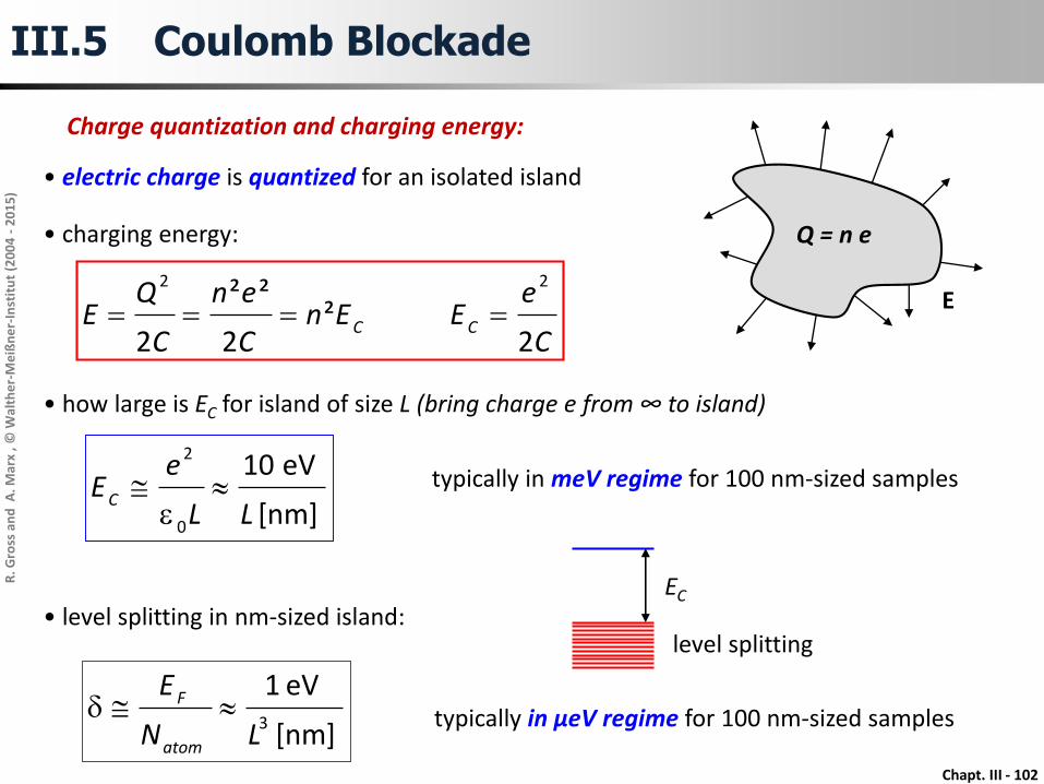
Charge quantization and charging energy:
• electric charge is quantized for an isolated island
Q = n e
E
C
eEEn
C
en
C
QE CC
2 ²
2
²²
2
22
[nm]
eV 10
0
2
LL
eEC
typically in meV regime for 100 nm-sized samples
[nm]
eV 13LN
E
atom
F typically in µeV regime for 100 nm-sized samples
EC
level splitting
• charging energy:
• how large is EC for island of size L (bring charge e from ∞ to island)
• level splitting in nm-sized island:
III.5 Coulomb Blockade

Chapt. III - 103
R. G
ross
and
A. M
arx
, © W
alth
er-
Me
ißn
er-
Inst
itu
t (2
00
4 -
20
15
)
Single Electron Box:
islandsource
gate: induces charge CGVG
VG
CG
tunnelingbarrier
C
+Q2-Q2+Q1-Q1
• electrostatic energy:
work done by the voltage source
• boundary conditions:
charge quantization on island
voltage drops over two capacitors
• with induced charge Q = CgVg:
III.5 Coulomb Blockade

Chapt. III - 104
R. G
ross
and
A. M
arx
, © W
alth
er-
Me
ißn
er-
Inst
itu
t (2
00
4 -
20
15
)
• electrostatic energy:
EC
constant term (independent of N)is omitted
Q = CgVg
III.5 Coulomb Blockade
thermalfluctuations
ground state
𝑘𝐵𝑇
Chapt. III - 107
R. G
ross
and
A. M
arx
, © W
alth
er-
Me
ißn
er-
Inst
itu
t (2
00
4 -
20
15
)
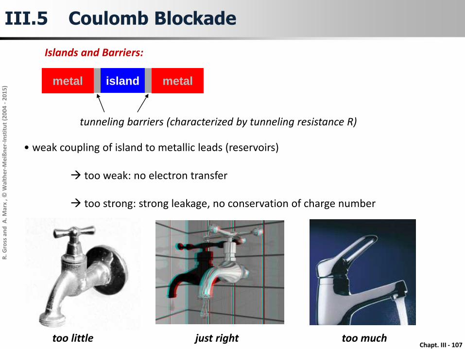
Islands and Barriers:
islandmetal metal
tunneling barriers (characterized by tunneling resistance R)
• weak coupling of island to metallic leads (reservoirs)
too weak: no electron transfer
too strong: strong leakage, no conservation of charge number
too little just right too much
III.5 Coulomb Blockade
Chapt. III - 108
R. G
ross
and
A. M
arx
, © W
alth
er-
Me
ißn
er-
Inst
itu
t (2
00
4 -
20
15
)
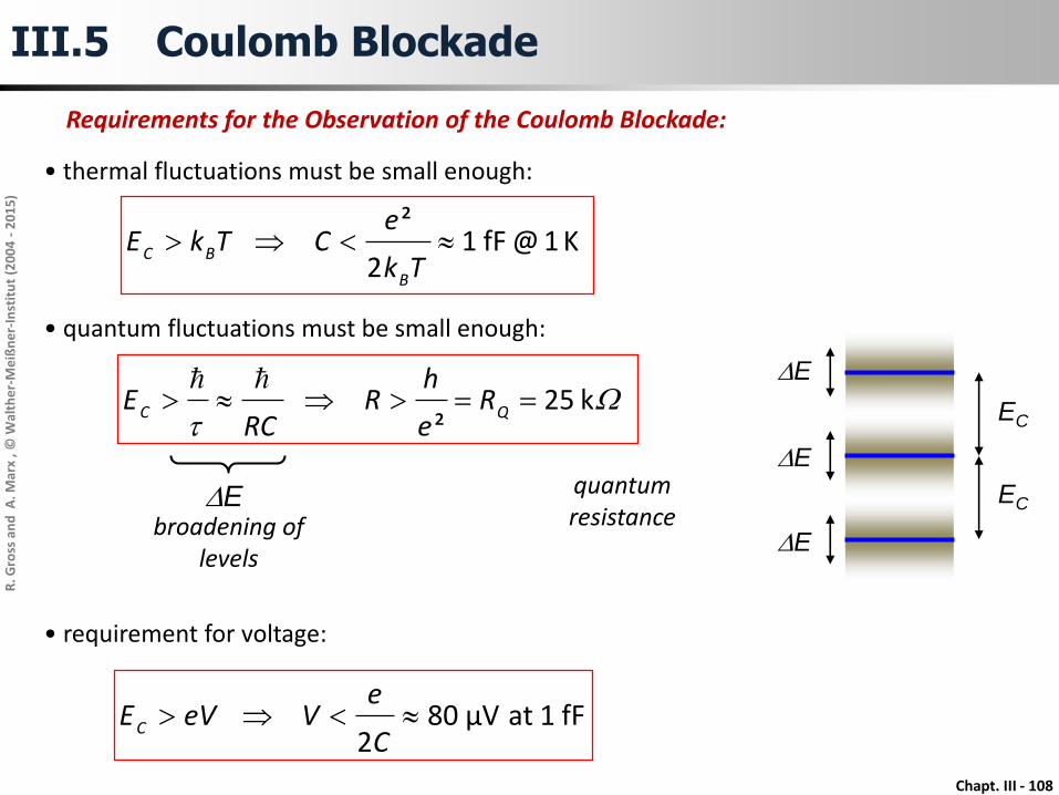
Requirements for the Observation of the Coulomb Blockade:
• thermal fluctuations must be small enough:
K 1 @ fF 12
²
Tk
eCTkE
B
BC
fF 1 at µV 802
C
eVeVEC
EC
EC
DE
DE
DE
k 25²
Wt
QC Re
hR
RCE
quantumresistance
DEbroadening of
levels
• quantum fluctuations must be small enough:
• requirement for voltage:
III.5 Coulomb Blockade
Chapt. III - 109
R. G
ross
and
A. M
arx
, © W
alth
er-
Me
ißn
er-
Inst
itu
t (2
00
4 -
20
15
)
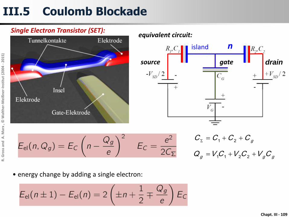
Single Electron Transistor (SET):
gCCCC 21
ggg CVCVCVQ 2211
• energy change by adding a single electron:
III.5 Coulomb Blockade
V1 V2
equivalent circuit:
source drain
island
gate
n
Chapt. III - 110
R. G
ross
and
A. M
arx
, © W
alth
er-
Me
ißn
er-
Inst
itu
t (2
00
4 -
20
15
)
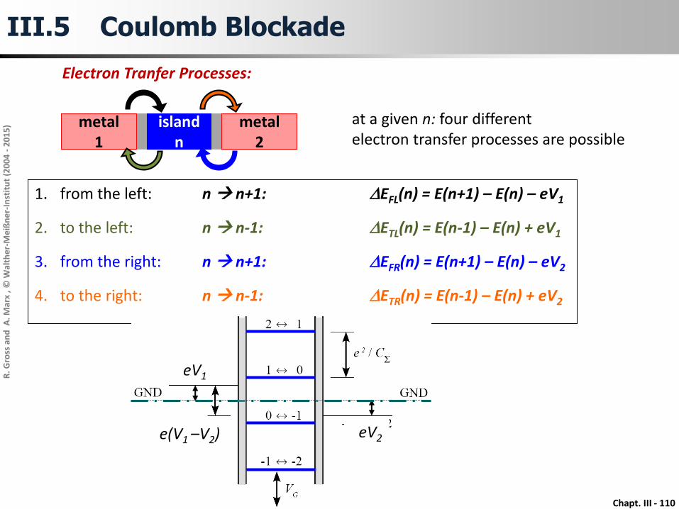
Electron Tranfer Processes:
islandn
metal1
metal2
at a given n: four differentelectron transfer processes are possible
1. from the left: n n+1: DEFL(n) = E(n+1) – E(n) – eV1
2. to the left: n n-1: DETL(n) = E(n-1) – E(n) + eV1
3. from the right: n n+1: DEFR(n) = E(n+1) – E(n) – eV2
4. to the right: n n-1: DETR(n) = E(n-1) – E(n) + eV2
e(V1 –V2)
eV1
eV2
III.5 Coulomb Blockade

Chapt. III - 111
R. G
ross
and
A. M
arx
, © W
alth
er-
Me
ißn
er-
Inst
itu
t (2
00
4 -
20
15
)
• T > 0: all transfer processes are allowed (by thermal activation)
Coulomb blockade
DEFL,TL,FR,TR (n) > 0
single electron tunneling
DEFL (n) < 0 DETR (n) < 0
DEFL (n+1) > 0
no second additional or missingelectron on island !!
Electron Tranfer Processes:
n+1
n+2
n
n-1
• T = 0: only transfer processes with DE < 0 are allowed
III.5 Coulomb Blockade
DETR (n-1) > 0
n+1
n
n-1
n-2
Chapt. III - 112
R. G
ross
and
A. M
arx
, © W
alth
er-
Me
ißn
er-
Inst
itu
t (2
00
4 -
20
15
)
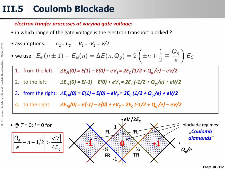
electron tranfer processes at varying gate voltage:
• in which range of the gate voltage is the electron transport blocked ?
1. from the left: DEFL(0) = E(1) – E(0) – eV1 = 2EC (1/2 + Qg /e) – eV/2
2. to the left: DETL(0) = E(-1) – E(0) + eV1 = 2EC (-1/2 + Qg /e) + eV/2
3. from the right: DEFR(0) = E(1) – E(0) – eV2 = 2EC (1/2 + Qg /e) + eV/2
4. to the right: DETR(0) = E(-1) – E(0) + eV2 = 2EC (-1/2 + Qg /e) – eV/2
blockade regimes:„Coulomb diamonds“
• @ T = 0: I = 0 for
C
g
E
Ven
e
Q
421
Qg/e
eV /2EC
FR TR
TLFL
½ -½
1
-1
• assumptions: C1 = C2 V1 = -V2 = V/2
• we use
III.5 Coulomb Blockade
0 +1 -1

Chapt. III - 113
R. G
ross
and
A. M
arx
, © W
alth
er-
Me
ißn
er-
Inst
itu
t (2
00
4 -
20
15
)
Single Electron Transistor – Coulomb Diamonds:
Quelle: ETH Zürich
Vg (mV)
V (m
V)
G (µS)
blue regions of vanishing conductance correspond tothe Coulomb blockade regime (no
current flow)
III.5 Coulomb Blockade
Chapt. III - 114
R. G
ross
and
A. M
arx
, © W
alth
er-
Me
ißn
er-
Inst
itu
t (2
00
4 -
20
15
)
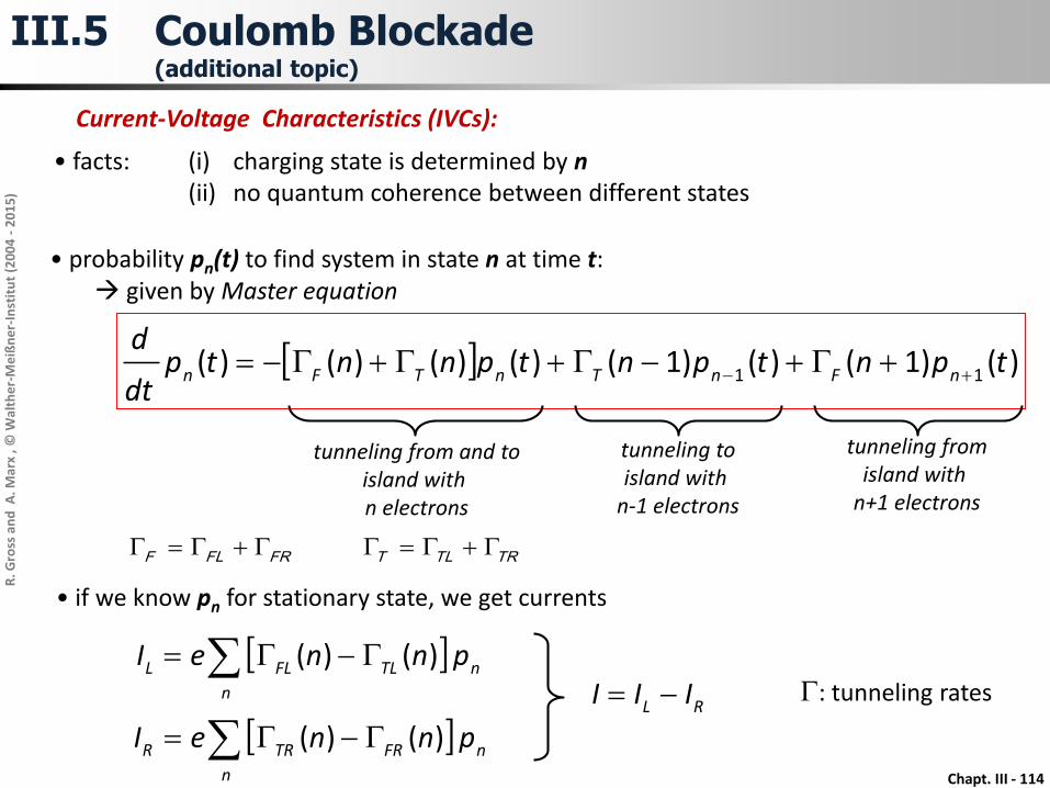
Current-Voltage Characteristics (IVCs):
• facts: (i) charging state is determined by n(ii) no quantum coherence between different states
n
n
TLFLL pnneI )()(
n
n
FRTRR pnneI )()( RL III : tunneling rates
• if we know pn for stationary state, we get currents
)()1()()1()()()()( 11 tpntpntpnntpdt
dnFnTnTFn
tunneling from and toisland withn electrons
tunneling toisland with
n-1 electrons
tunneling fromisland with
n+1 electrons
FRFLF TRTLT
• probability pn(t) to find system in state n at time t: given by Master equation
III.5 Coulomb Blockade(additional topic)

Chapt. III - 115
R. G
ross
and
A. M
arx
, © W
alth
er-
Me
ißn
er-
Inst
itu
t (2
00
4 -
20
15
)
Tunneling Rates for Single Tunnel Junction:
tunneling without CB
VGI T
tunneling rate:
eVe
G
e
I T
²
tunneling with CB
eV
energy intervalfor available final states
tunneling rate:
CT
C EeVe
GEeV
² :
0 : CEeV
eVEC
energy intervalfor available final states
eV- EC
blockade regime
III.5 Coulomb Blockade
Chapt. III - 116
R. G
ross
and
A. M
arx
, © W
alth
er-
Me
ißn
er-
Inst
itu
t (2
00
4 -
20
15
)
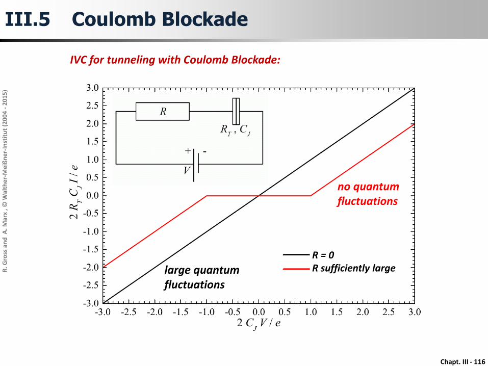
IVC for tunneling with Coulomb Blockade:
R = 0R sufficiently large
no quantumfluctuations
large quantumfluctuations
III.5 Coulomb Blockade
Chapt. III - 117
R. G
ross
and
A. M
arx
, © W
alth
er-
Me
ißn
er-
Inst
itu
t (2
00
4 -
20
15
)
Tunneling Rates and IVC:
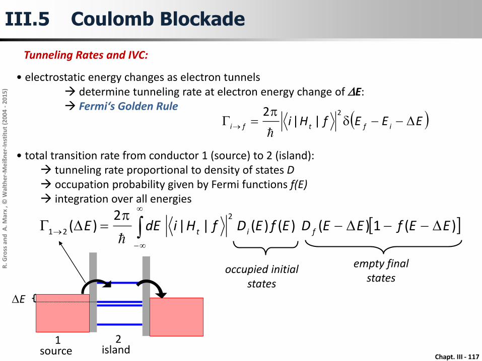
• electrostatic energy changes as electron tunnels determine tunneling rate at electron energy change of DE: Fermi‘s Golden Rule
EEEfHi iftfi Dp
2
||2
)(1)( )()( || 2
)(2
21 EEfEEDEfEDfHidEE fit DDp
D
empty finalstates
occupied initialstates
2
DE
1source island
• total transition rate from conductor 1 (source) to 2 (island): tunneling rate proportional to density of states D occupation probability given by Fermi functions f(E) integration over all energies
III.5 Coulomb Blockade
Chapt. III - 118
R. G
ross
and
A. M
arx
, © W
alth
er-
Me
ißn
er-
Inst
itu
t (2
00
4 -
20
15
)
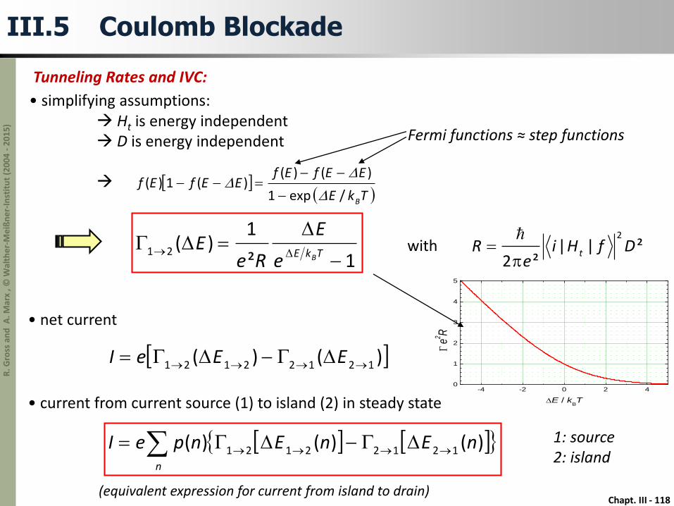
• simplifying assumptions: Ht is energy independent D is energy independent
TkE
EEfEfEEfEf
B/exp1
)()()(1)(
D
DD
²||²2
2
DfHie
R tp
with
)()( 12122121 DD EEeI
DD
n
nEnEnpeI )()()( 121221211: source2: island
1²
1)(21
DD
D TkE Be
E
ReE
Fermi functions ≈ step functions
(equivalent expression for current from island to drain)
Tunneling Rates and IVC:
• net current
• current from current source (1) to island (2) in steady state
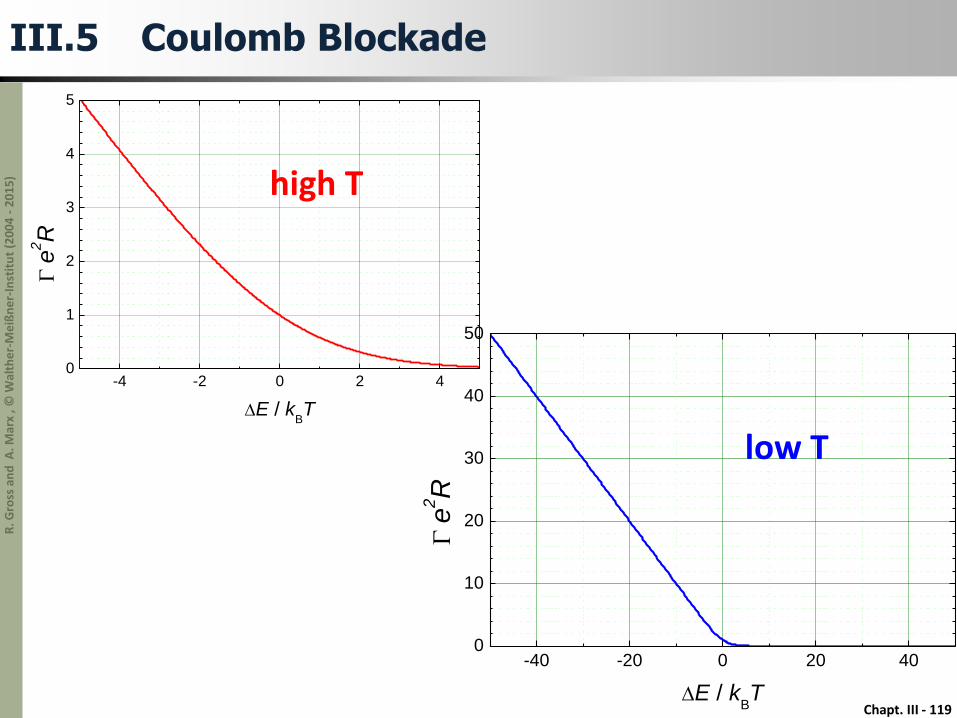
III.5 Coulomb Blockade
-4 -2 0 2 40
1
2
3
4
5
e2 R
DE / kBT
Chapt. III - 119
R. G
ross
and
A. M
arx
, © W
alth
er-
Me
ißn
er-
Inst
itu
t (2
00
4 -
20
15
)
-40 -20 0 20 400
10
20
30
40
50
e
2R
DE / kBT
-4 -2 0 2 40
1
2
3
4
5
e
2R
DE / kBT
high T
low T
III.5 Coulomb Blockade

Chapt. III - 120
R. G
ross
and
A. M
arx
, © W
alth
er-
Me
ißn
er-
Inst
itu
t (2
00
4 -
20
15
)
Quelle: ETH Zürich
Coulombdiamonds
Tunneling Rates and IVC:
III.5 Coulomb Blockade

Chapt. III - 121
R. G
ross
and
A. M
arx
, © W
alth
er-
Me
ißn
er-
Inst
itu
t (2
00
4 -
20
15
)
Quelle: lt.px.tsukuba.ac.jp
V
Imovie shows variation of IVC with varyinggate voltage
Tunneling Rates and IVC – Coulomb Staircase:
1st step in IVC
2nd step in IVC
ground
Vg
V/2
V/2
groundV/2V/2
Vg
III.5 Coulomb Blockade
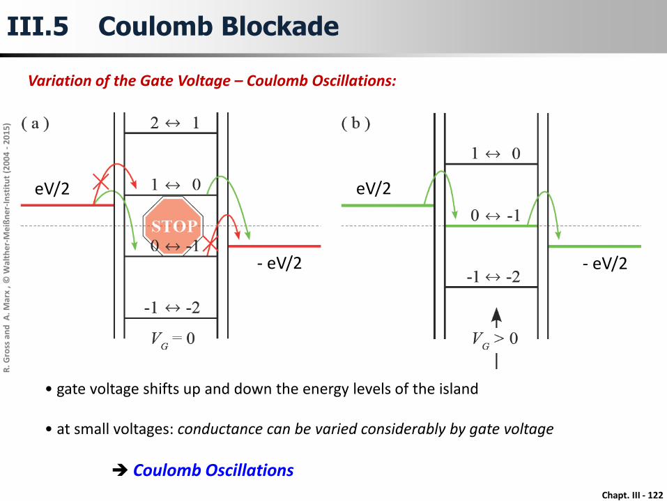
Chapt. III - 122
R. G
ross
and
A. M
arx
, © W
alth
er-
Me
ißn
er-
Inst
itu
t (2
00
4 -
20
15
)
Variation of the Gate Voltage – Coulomb Oscillations:
eV/2
- eV/2
eV/2
- eV/2
• gate voltage shifts up and down the energy levels of the island
• at small voltages: conductance can be varied considerably by gate voltage
Coulomb Oscillations
III.5 Coulomb Blockade
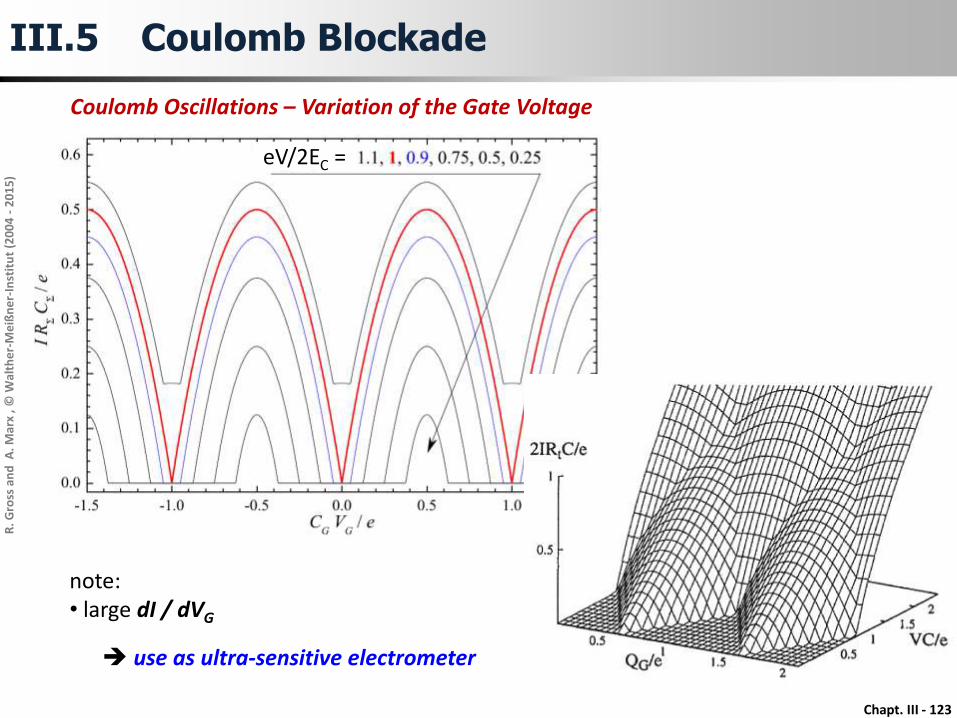
Chapt. III - 123
R. G
ross
and
A. M
arx
, © W
alth
er-
Me
ißn
er-
Inst
itu
t (2
00
4 -
20
15
)
Coulomb Oscillations – Variation of the Gate Voltage
eV/2EC =
note:• large dI / dVG
use as ultra-sensitive electrometer
III.5 Coulomb Blockade
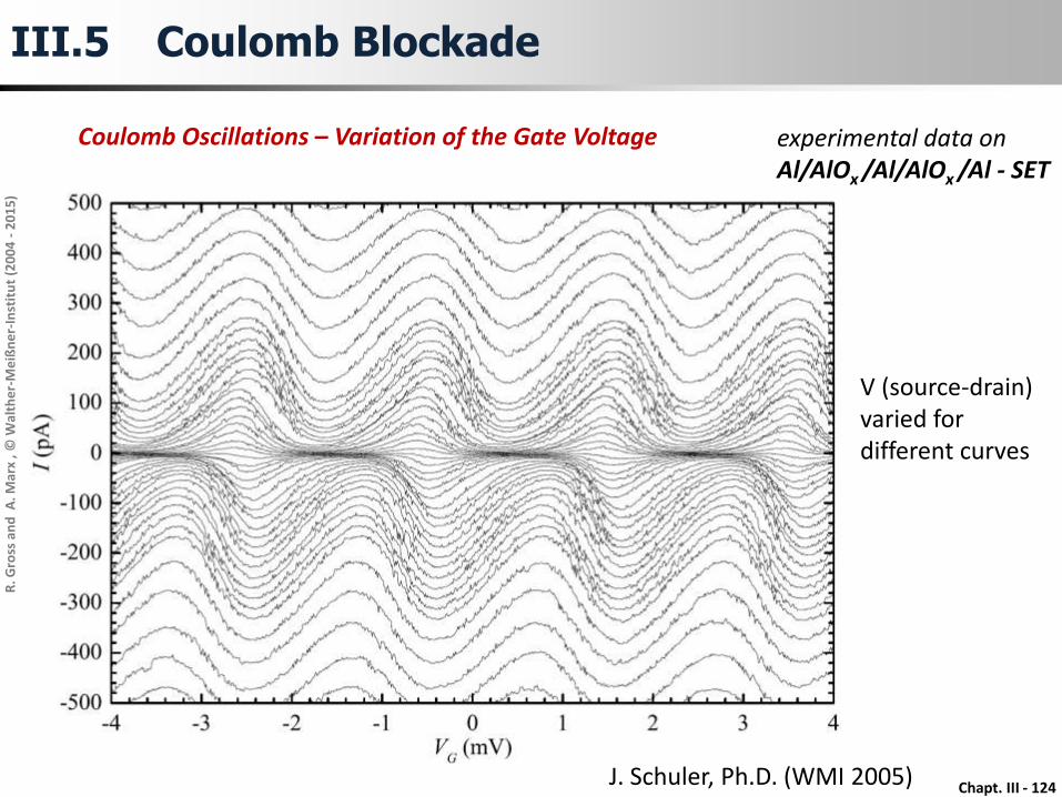
Chapt. III - 124
R. G
ross
and
A. M
arx
, © W
alth
er-
Me
ißn
er-
Inst
itu
t (2
00
4 -
20
15
)
J. Schuler, Ph.D. (WMI 2005)
experimental data onAl/AlOx /Al/AlOx /Al - SET
V (source-drain)varied for different curves
Coulomb Oscillations – Variation of the Gate Voltage
III.5 Coulomb Blockade

Chapt. III - 125
R. G
ross
and
A. M
arx
, © W
alth
er-
Me
ißn
er-
Inst
itu
t (2
00
4 -
20
15
)
Coulomb Oscillations – Effect of Single Fluctuating Background Charges
J. Schuler, Ph.D. (WMI 2005)
Al/AlOx/Al/AlOx/Al - SET
shift of I(Vg)curve due tofluctuatingbackgroundcharge
III.5 Coulomb Blockade
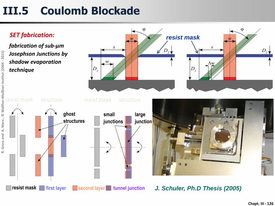
Chapt. III - 126
R. G
ross
and
A. M
arx
, © W
alth
er-
Me
ißn
er-
Inst
itu
t (2
00
4 -
20
15
)
SET fabrication:
resist mask structure resist mask structure
resist mask first layer second layer tunnel junction
ghost
structures
small
junctions
large
junction
J. Schuler, Ph.D Thesis (2005)
fabrication of sub-µm
Josephson Junctions by
shadow evaporation
technique
resist mask
III.5 Coulomb Blockade
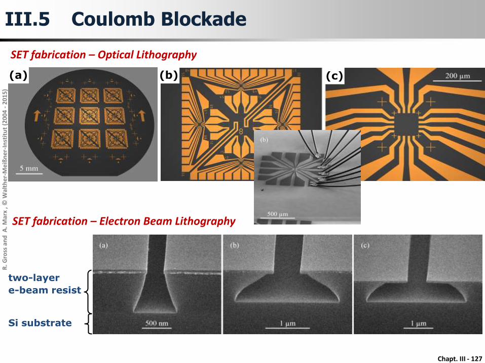
Chapt. III - 127
R. G
ross
and
A. M
arx
, © W
alth
er-
Me
ißn
er-
Inst
itu
t (2
00
4 -
20
15
)
SET fabrication – Optical Lithography
(a) (b) (c)
two-layer
e-beam resist
Si substrate
SET fabrication – Electron Beam Lithography
III.5 Coulomb Blockade

Chapt. III - 128
R. G
ross
and
A. M
arx
, © W
alth
er-
Me
ißn
er-
Inst
itu
t (2
00
4 -
20
15
)
shadow evaporation
substrate
resist layer 1
resist layer 2
first evaporation of Aloxidation of 1st Al layer
2nd evaporation of Al
after liftoff

Chapt. III - 129
R. G
ross
and
A. M
arx
, © W
alth
er-
Me
ißn
er-
Inst
itu
t (2
00
4 -
20
15
)
gate
source drain
tunnel
junctions
gate
islandAl Al
1µm
tunnel junctions
III.5 Coulomb BlockadeSET Fabrication

Chapt. III - 130
R. G
ross
and
A. M
arx
, © W
alth
er-
Me
ißn
er-
Inst
itu
t (2
00
4 -
20
15
)
Applications:
• sensitive electrometers: Q/Q ≈ 10-5 e
• electron pumps
transporting electrons one by one: counting of electrons
current standard: I = e f application of oscillating gate voltage
• charge Qubits
basic element for quantum information systems
Quantum oscillations in two coupled charge qubitsYu. A. Pashkin, T. Yamamoto, O. Astafiev, Y. Nakamura, D. V. Averin and J. S. TsaiNature 421, 823-826(20 February 2003)
PTB
III.5 Coulomb Blockade

Chapt. III - 131
R. G
ross
and
A. M
arx
, © W
alth
er-
Me
ißn
er-
Inst
itu
t (2
00
4 -
20
15
)
III.5 Coulomb Blockade
frequency
voltage current𝑽 = 𝑹𝑲 ⋅ 𝑰
quantum metrological
triangle
• 1990:
KI-90 = 1/e not yet availabe