chapter 4shodhganga.inflibnet.ac.in/bitstream/10603/26645/9/09_chapter 4.pdf · fpga and dsp based...
TRANSCRIPT
104
CHAPTER 4
IMPLEMENTATION OF SVPWM BASED OPEN LOOP V/Hz
CONTROL OF INDUCTION MOTOR USING DSP AND FPGA
4.1 INTRODUCTION
The most common principle of induction motor control is the
constant V/Hz control (also referred as V/f control) that requires the ratio of
magnitude and frequency of the voltage applied to the stator of the motor
which is maintained constant. By doing this, the magnitude of the magnetic
field in the stator is kept at an approximately constant level throughout the
operating range. Thus (maximum) constant torque producing capability is
maintained.
When the transient response is critical, switching power converters
also allow easy control of transient voltage and current applied to the motor to
achieve faster dynamic response. PWM signals applied to the gates of the
power switches control the energy that a switching power converter delivers
to a motor.
Traditional software-based systems have disadvantages of complex
circuitry, limited functions, difficult circuit modification, high cost and low
execution speed. The advent of Very Large Scale Integration (VLSI)
technology has given FPGAs a rapid growth in importance with wide range of
105
applications. DSPs allow implementation of advanced algorithms as well as
reduction in system cost.
In what follows, DSP and FPGA Based Constant V/Hz speed
control of three phase induction motor using the SVPWM technique is
presented here under.
4 .2 CONSTANT V/Hz CONTROL OF AC MOTOR
The evolution on the operation of induction machines in constant volts per hertz mode back goes back to the late fifties and early sixties but were limited in their low speed range. Today constant volts per hertz drives are built using PWM-IGBT based inverters and the speed range has widened to include very low speeds, although the operation at very near-zero speed (less than 1 Hz) remains as a challenge mainly due to the inverter non-linearities at low output voltages.
4.2.1 Principle of voltage control
By keeping a constant V/Hz ratio for all frequencies, the nominal
torque-speed curve of the induction motor can be reproduced at any
frequency. This simple and straight forward approach however does not work
well in reality due to several factors. The most important factors are:
1. Effect of supply voltage variations
2. Influence of stator resistance
3. Non-ideal torque/speed characteristic (effects of slip) and
4. Non-linearities introduced by the PWM inverter.
Low frequency operation is particularly difficult to achieve, since
these effects are most prominent at low voltages. Also the non-linearities
within the inverter if not adequately compensated, yield highly distorted
106
output voltages which in turn produces pulsating torques that lead to
vibrations and increased acoustic noise.
4.2.2 The constant V/Hz principle
Today constant Volts per Hertz principle is the most common
control principle used in adjustable-speed drives of induction machines (Bose
2004, Krishnan 2006). Hence many real-life motor control applications do not
need a high dynamic performance as long as the speed can be efficiently
varied in full range. Specifically, if stator resistance is neglected and by
keeping a constant slip frequency, the steady state behavior of the induction
machine can be characterized as impedance which is proportional to
frequency. Therefore, if the V/Hz ratio is kept constant, the stator flux, stator
current and variable-frequency induction motor drive’s torque will be
constant at any frequency. This feature suggests that to control the torque, one
need to simply apply the correct amount of V/Hz to stator windings.
More precisely, from the steady state model, an induction motor is
expressed in the fixed reference frame as given by Equations (4.1) to (4.5).
ssss VIR
dtd (4.1)
0IRjdt
drrrm
s (4.2)
rImLsIsLs (4.3)
sImLrIrLr (4.4)
107
)I(IL2
3PT *rsmem (4.5)
where Vs, s, r, Is, Ir, Im are respectively the stator voltage, stator and rotor
magnetic fluxes, stator, rotor and leakage currents and P, Rs, Rr, Ls, Lr, Lm and
m are respectively the number of poles, global stator resistance, rotor
resistance, stator inductance, rotor inductance, global leakage inductance and
angular speed.
If the motor is fed with a sinusoidal three phase voltage tjsms
seVV
with angular frequency s, the steady-state currents in the rotor and the stator
will also be sinusoids and expressed as )tj(sms
sseII and )tj(rmr
rseII
where s and r are the respective phase angles. These expressions lead to
Equations (4.6) and (4.7).
sslprr
s VjLR
I (4.6)
sslpm
r VjL
I (4.7)
where s is the stator angular frequency, slp = s - m and
=(Rs+jLs s)(Rr+jLr slp)+Lm2
slp s. Hence the rotor flux magnitude rm,
which is proportional to rotor current can be kept constant if the ratio Vsm is
kept constant.
108
At higher speed, = jRrLs s and the rotor flux magnitude is
constant if the ratio s
smV is kept constant leading to ss
smmrm L
VL . The motor
torque is then proportional to the slip frequency i.e., slp
r
rmem R
PT
23 2
. These
expressions show that a desired motor torque Tem and a desired motor speed
m can be obtained if 23
2
rm
remms P
RT . Also at low speed, = RsRr and
ss
mr V
RL .
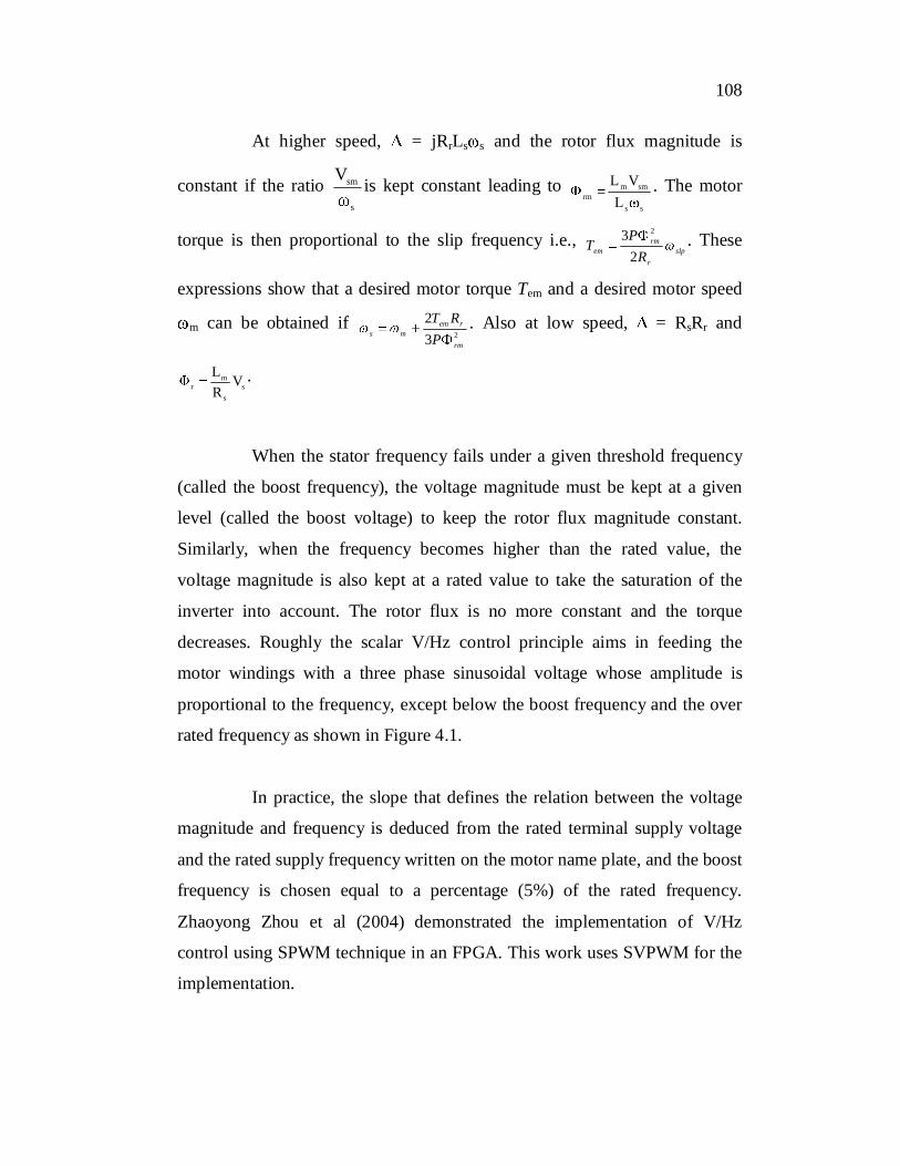
When the stator frequency fails under a given threshold frequency
(called the boost frequency), the voltage magnitude must be kept at a given
level (called the boost voltage) to keep the rotor flux magnitude constant.
Similarly, when the frequency becomes higher than the rated value, the
voltage magnitude is also kept at a rated value to take the saturation of the
inverter into account. The rotor flux is no more constant and the torque
decreases. Roughly the scalar V/Hz control principle aims in feeding the
motor windings with a three phase sinusoidal voltage whose amplitude is
proportional to the frequency, except below the boost frequency and the over
rated frequency as shown in Figure 4.1.
In practice, the slope that defines the relation between the voltage
magnitude and frequency is deduced from the rated terminal supply voltage
and the rated supply frequency written on the motor name plate, and the boost
frequency is chosen equal to a percentage (5%) of the rated frequency.
Zhaoyong Zhou et al (2004) demonstrated the implementation of V/Hz
control using SPWM technique in an FPGA. This work uses SVPWM for the
implementation.
109
frated fboostf
Vs
Vrated
Vboost
Figure 4.1 Stator voltage magnitude versus stator voltage frequency
deduced from the V/Hz Principle
4.3 EXPERIMENTAL SETUP
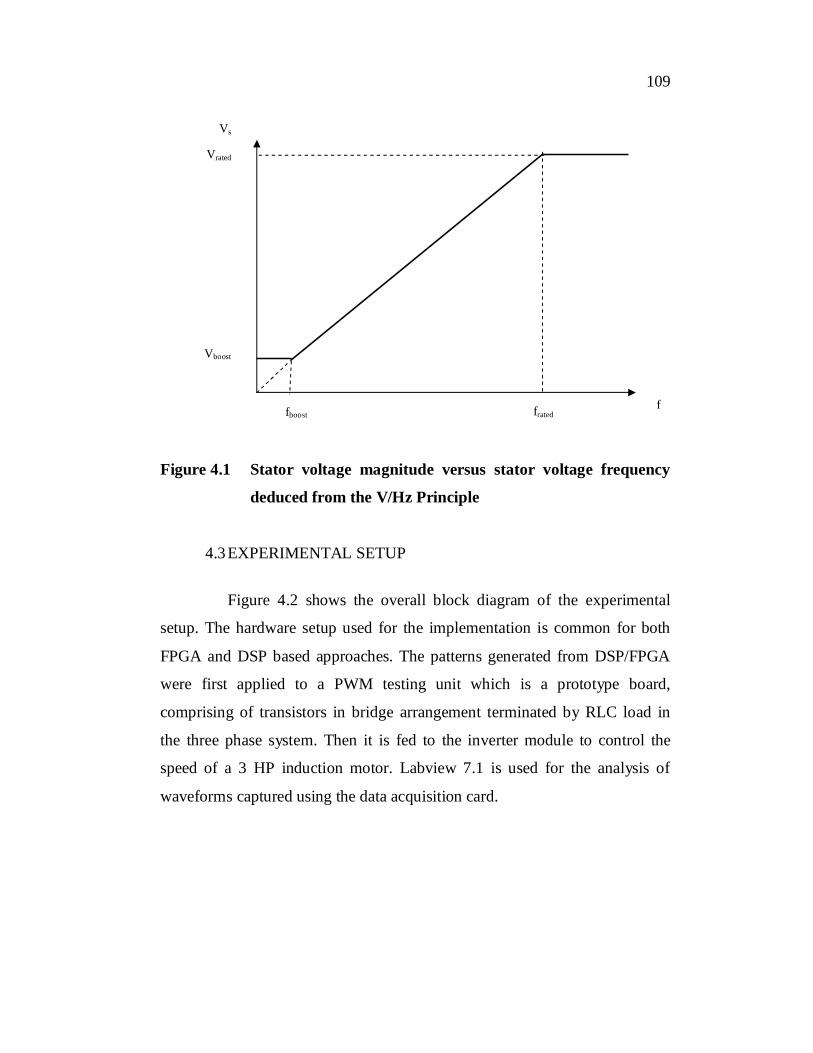
Figure 4.2 shows the overall block diagram of the experimental
setup. The hardware setup used for the implementation is common for both
FPGA and DSP based approaches. The patterns generated from DSP/FPGA
were first applied to a PWM testing unit which is a prototype board,
comprising of transistors in bridge arrangement terminated by RLC load in
the three phase system. Then it is fed to the inverter module to control the
speed of a 3 HP induction motor. Labview 7.1 is used for the analysis of
waveforms captured using the data acquisition card.
110
Figure 4.2 Block diagram of the experimental setup
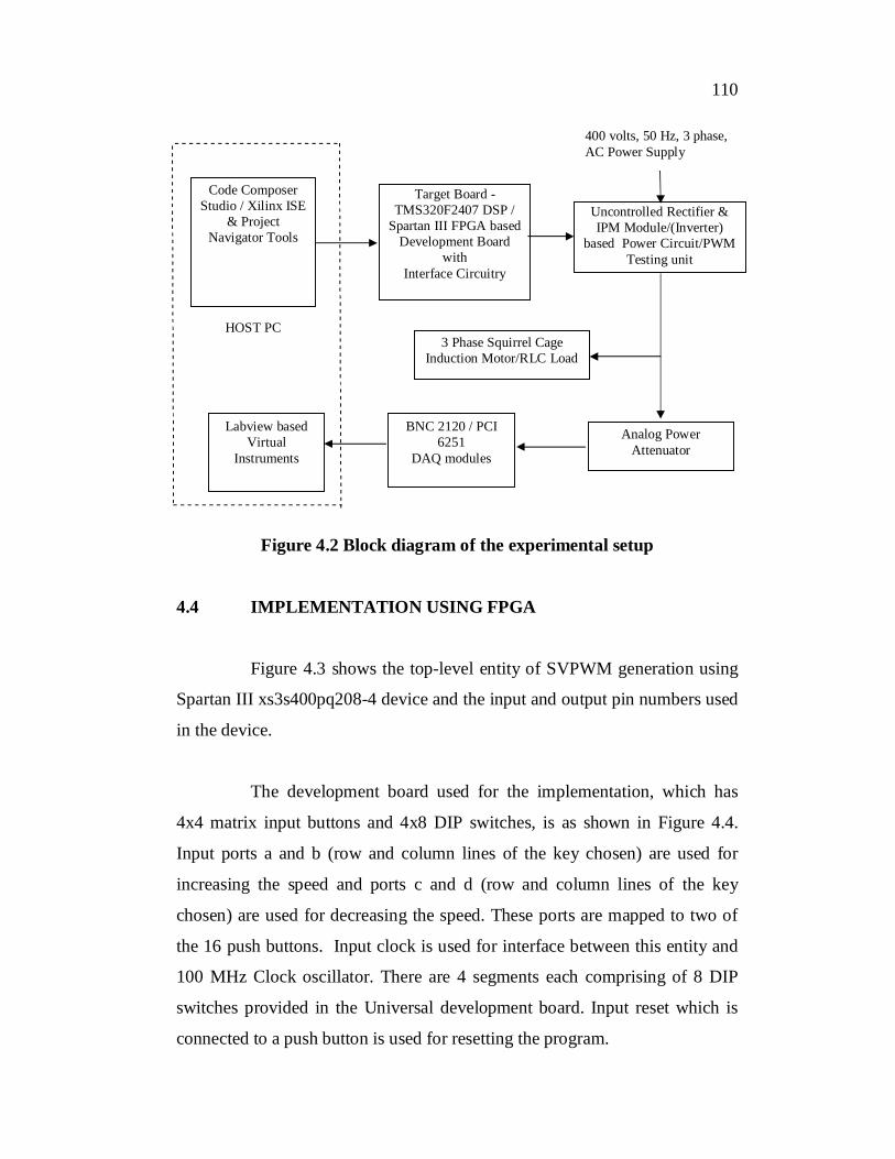
4.4 IMPLEMENTATION USING FPGA
Figure 4.3 shows the top-level entity of SVPWM generation using
Spartan III xs3s400pq208-4 device and the input and output pin numbers used
in the device.
The development board used for the implementation, which has
4x4 matrix input buttons and 4x8 DIP switches, is as shown in Figure 4.4.
Input ports a and b (row and column lines of the key chosen) are used for
increasing the speed and ports c and d (row and column lines of the key
chosen) are used for decreasing the speed. These ports are mapped to two of
the 16 push buttons. Input clock is used for interface between this entity and
100 MHz Clock oscillator. There are 4 segments each comprising of 8 DIP
switches provided in the Universal development board. Input reset which is
connected to a push button is used for resetting the program.
Code Composer Studio / Xilinx ISE
& Project Navigator Tools
Target Board -TMS320F2407 DSP /
Spartan III FPGA based Development Board
with Interface Circuitry
Uncontrolled Rectifier & IPM Module/(Inverter)
based Power Circuit/PWM Testing unit
3 Phase Squirrel Cage Induction Motor/RLC Load
Analog Power Attenuator
BNC 2120 / PCI 6251
DAQ modules
Labview based Virtual
Instruments
HOST PC
400 volts, 50 Hz, 3 phase,AC Power Supply
111
The board has 264 external I/O connectors. Out of these, six I/O
connectors are used for sending out the pulses from the development board.
Pins p50, p51, p52, p57, p58 and p61 are used for this purpose. There are 32
red LEDs provided in the universal development board. p22, p24, p26, p27
and p28 are the five outputs connected to the LEDs to show the step value.
Figure 4.3 Top level entity – SVPWM based V/Hz control
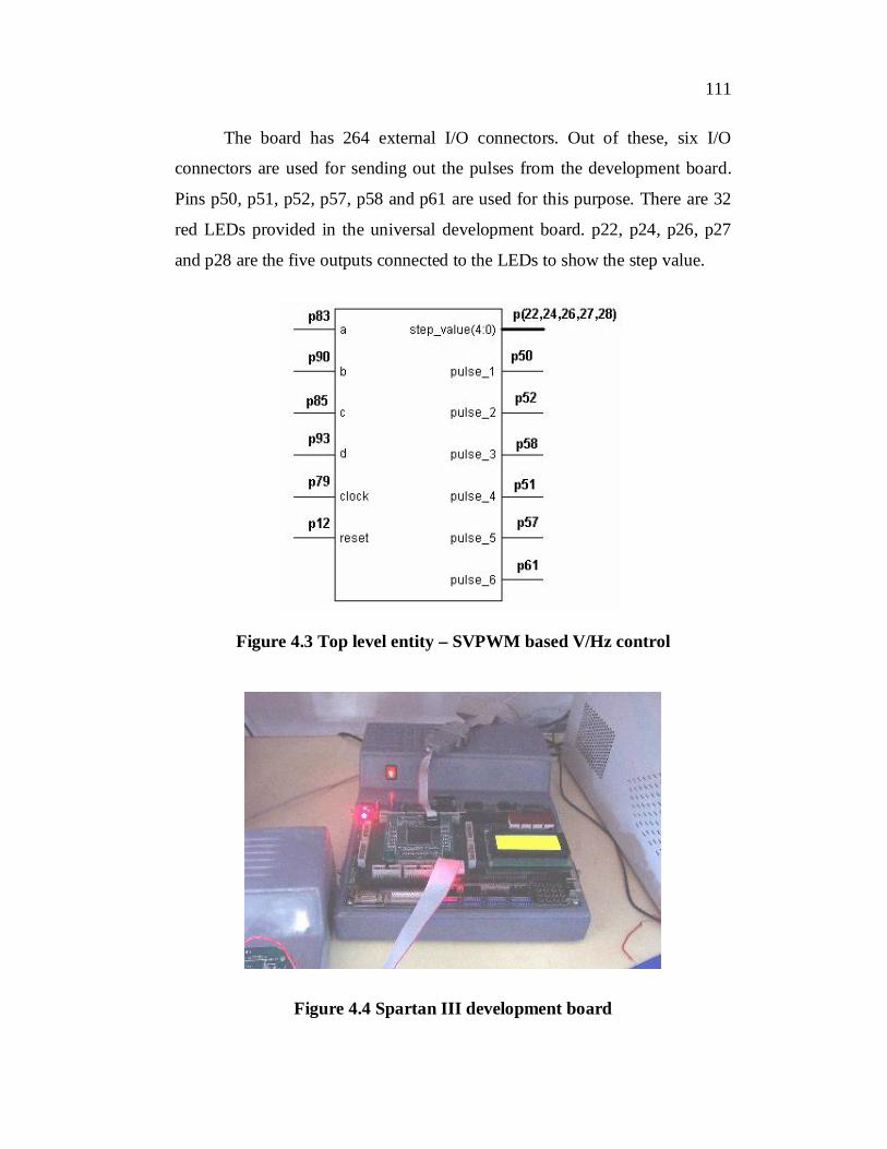
Figure 4.4 Spartan III development board

112
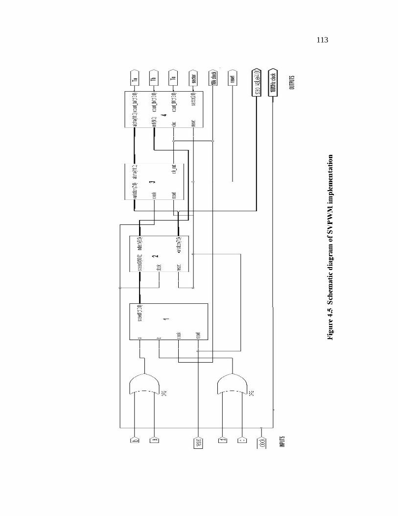
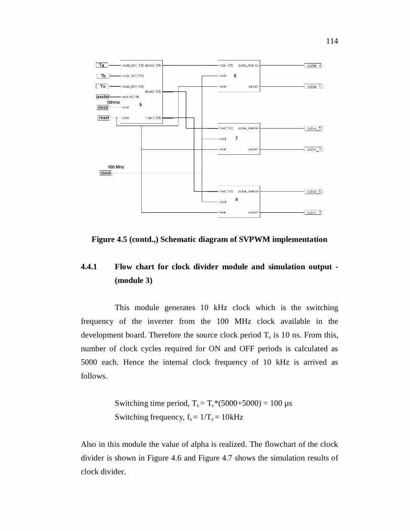
This implementation contains eight modules namely (modules are
listed with the serial number same as given in Figure 4.5)
1. Speed variation depending up on the given push button input
2. Calculation of modulation index and step value (variation)
3. Clock divider
4. Calculation of Ta, Tb and To
5. Calculation of the number of 100 Mhz pulses for ON time
pulse duration for six SCRs.
6. Pulse generation for Thyristor 1 and Thyristor 4
7. Pulse generation for Thyristor 2 and Thyristor 5
8. Pulse generation for Thyristor 3 and Thyristor 6.
In sections 4.3.1.1 to 4.3.1.5 the algorithms of the above mentioned
sub-modules are discussed.
113
114
Figure 4.5 (contd.,) Schematic diagram of SVPWM implementation
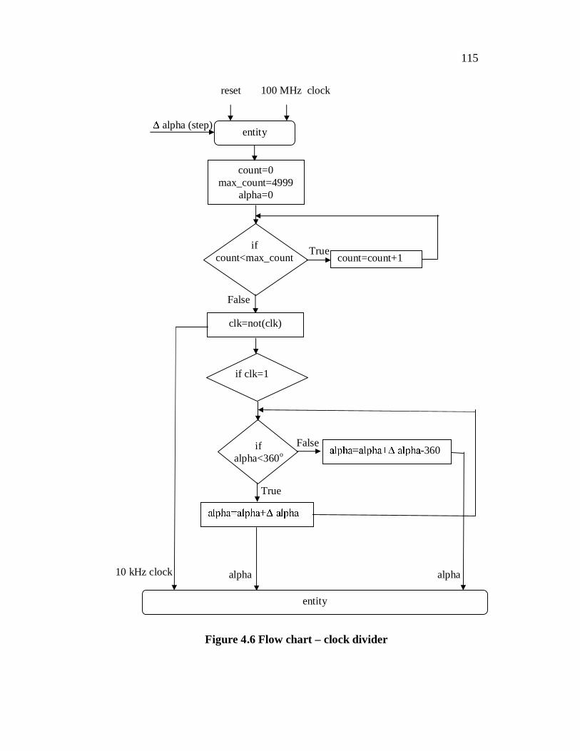
4.4.1 Flow chart for clock divider module and simulation output -
(module 3)
This module generates 10 kHz clock which is the switching
frequency of the inverter from the 100 MHz clock available in the
development board. Therefore the source clock period Tc is 10 ns. From this,
number of clock cycles required for ON and OFF periods is calculated as
5000 each. Hence the internal clock frequency of 10 kHz is arrived as
follows.
Switching time period, Ts = Tc*(5000+5000) = 100 µs
Switching frequency, fs = 1/Ts = 10kHz
Also in this module the value of alpha is realized. The flowchart of the clock
divider is shown in Figure 4.6 and Figure 4.7 shows the simulation results of
clock divider.
115
Figure 4.6 Flow chart – clock divider
count=0max_count=4999
alpha=0
count=count+1
clk=not(clk)
-360
if clk=1
entity
entity
if count<max_count
ifalpha<360o
False
True
alpha (step)
reset 100 MHz clock
False
True
alpha alpha 10 kHz clock
116
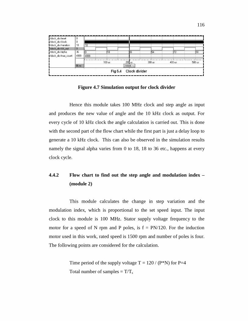
Figure 4.7 Simulation output for clock divider
Hence this module takes 100 MHz clock and step angle as input
and produces the new value of angle and the 10 kHz clock as output. For
every cycle of 10 kHz clock the angle calculation is carried out. This is done
with the second part of the flow chart while the first part is just a delay loop to
generate a 10 kHz clock. This can also be observed in the simulation results
namely the signal alpha varies from 0 to 18, 18 to 36 etc., happens at every
clock cycle.
4.4.2 Flow chart to find out the step angle and modulation index –
(module 2)
This module calculates the change in step variation and the
modulation index, which is proportional to the set speed input. The input
clock to this module is 100 MHz. Stator supply voltage frequency to the
motor for a speed of N rpm and P poles, is f = PN/120. For the induction
motor used in this work, rated speed is 1500 rpm and number of poles is four.
The following points are considered for the calculation.
Time period of the supply voltage T = 120 / (P*N) for P=4
Total number of samples = T/Ts
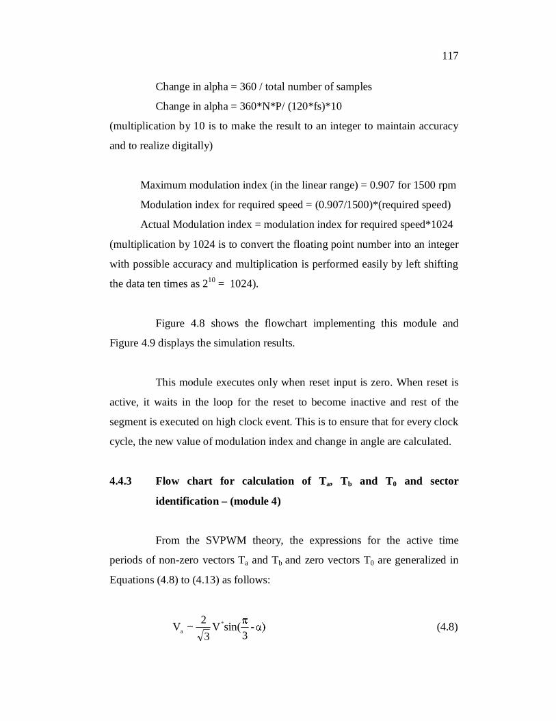
117
Change in alpha = 360 / total number of samples
Change in alpha = 360*N*P/ (120*fs)*10
(multiplication by 10 is to make the result to an integer to maintain accuracy
and to realize digitally)
Maximum modulation index (in the linear range) = 0.907 for 1500 rpm
Modulation index for required speed = (0.907/1500)*(required speed)
Actual Modulation index = modulation index for required speed*1024
(multiplication by 1024 is to convert the floating point number into an integer
with possible accuracy and multiplication is performed easily by left shifting
the data ten times as 210 = 1024).
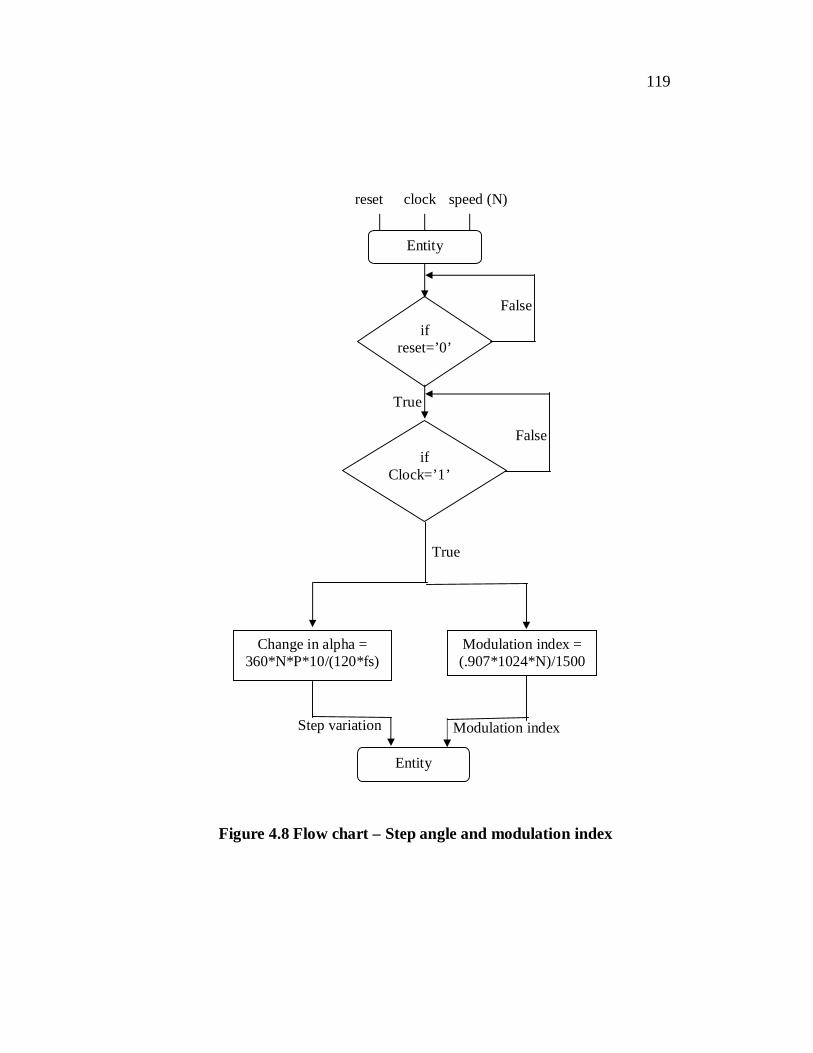
Figure 4.8 shows the flowchart implementing this module and
Figure 4.9 displays the simulation results.
This module executes only when reset input is zero. When reset is
active, it waits in the loop for the reset to become inactive and rest of the
segment is executed on high clock event. This is to ensure that for every clock
cycle, the new value of modulation index and change in angle are calculated.
4.4.3 Flow chart for calculation of Ta, Tb and T0 and sector
identification – (module 4)
From the SVPWM theory, the expressions for the active time
periods of non-zero vectors Ta and Tb and zero vectors T0 are generalized in
Equations (4.8) to (4.13) as follows:
-3
sin(V3
2V *a (4.8)
118
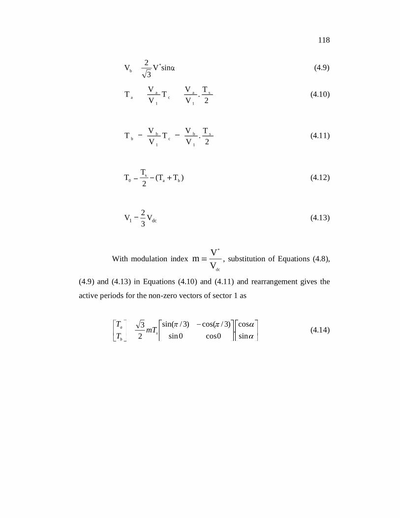
sinV3
2V *b (4.9)
2
T.VVT
VVT s
1
ac
1
aa (4.10)
2
T.VVT
VVT s
1
bc
1
bb (4.11)
)T(T2T
T bas
0 (4.12)
dc1 V32V (4.13)
With modulation index dc
*
VVm , substitution of Equations (4.8),
(4.9) and (4.13) in Equations (4.10) and (4.11) and rearrangement gives the
active periods for the non-zero vectors of sector 1 as
sincos
.0cos0sin
)3/cos()3/sin(23
sb
a mTTT
(4.14)
119
Figure 4.8 Flow chart – Step angle and modulation index
if reset=’0’
if Clock=’1’
Change in alpha = 360*N*P*10/(120*fs)
Modulation index = (.907*1024*N)/1500
Entity
Entity
reset clock speed (N)
True
True
Modulation indexStep variation
False
False
120
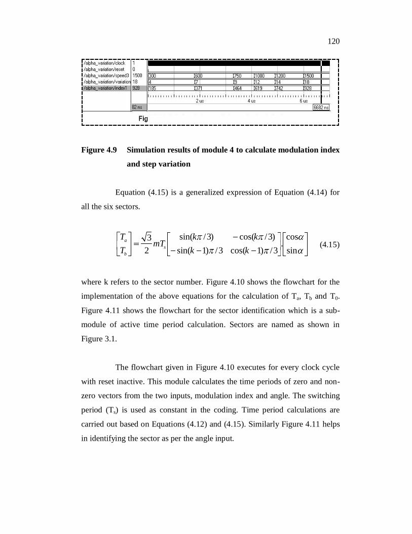
Figure 4.9 Simulation results of module 4 to calculate modulation index
and step variation
Equation (4.15) is a generalized expression of Equation (4.14) for
all the six sectors.
sincos
.3/)1cos(3/)1sin()3/cos()3/sin(
23
kkkk
mTTT
sb
a (4.15)
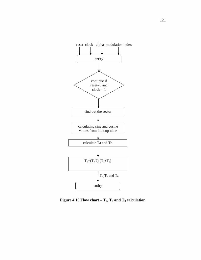
where k refers to the sector number. Figure 4.10 shows the flowchart for the
implementation of the above equations for the calculation of Ta, Tb and T0.
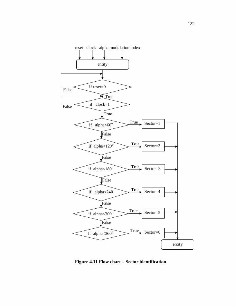
Figure 4.11 shows the flowchart for the sector identification which is a sub-
module of active time period calculation. Sectors are named as shown in
Figure 3.1.
The flowchart given in Figure 4.10 executes for every clock cycle
with reset inactive. This module calculates the time periods of zero and non-
zero vectors from the two inputs, modulation index and angle. The switching
period (Ts) is used as constant in the coding. Time period calculations are
carried out based on Equations (4.12) and (4.15). Similarly Figure 4.11 helps
in identifying the sector as per the angle input.
121
reset clock alpha modulation index
entity
continue if reset=0 and clock = 1
calculating sine and cosine values from look up table
find out the sector
calculate Ta and Tb
T0=(Ts/2)-(Ta+Tb)
entity
Ta, Tb and T0
Figure 4.10 Flow chart – Ta, Tb and T0 calculation
122
Figure 4.11 Flow chart – Sector identification
entity
if reset=0
if clock=1
if alpha<60o
if alpha<120o
if alpha<180o
if alpha<240
if alpha<300o
If alpha<360o
Sector=1
Sector=2
Sector=3
Sector=4
Sector=5
Sector=6
entity
reset clock alpha modulation index
True
True
True
True
True
True
False
False
False
False
False
False
True
True False
123
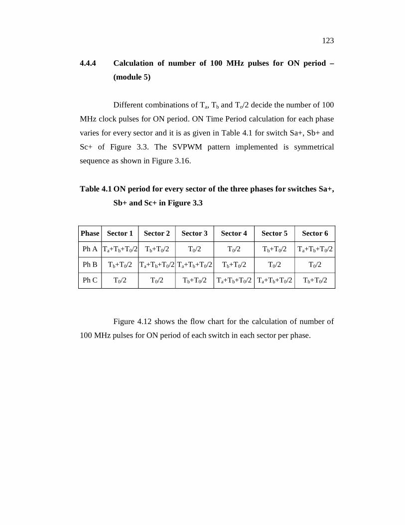
4.4.4 Calculation of number of 100 MHz pulses for ON period –
(module 5)
Different combinations of Ta, Tb and To/2 decide the number of 100
MHz clock pulses for ON period. ON Time Period calculation for each phase
varies for every sector and it is as given in Table 4.1 for switch Sa+, Sb+ and
Sc+ of Figure 3.3. The SVPWM pattern implemented is symmetrical
sequence as shown in Figure 3.16.
Table 4.1 ON period for every sector of the three phases for switches Sa+,
Sb+ and Sc+ in Figure 3.3
Phase Sector 1 Sector 2 Sector 3 Sector 4 Sector 5 Sector 6
Ph A Ta+Tb+T0/2 Tb+T0/2 T0/2 T0/2 Tb+T0/2 Ta+Tb+T0/2
Ph B Tb+T0/2 Ta+Tb+T0/2 Ta+Tb+T0/2 Tb+T0/2 T0/2 T0/2
Ph C T0/2 T0/2 Tb+T0/2 Ta+Tb+T0/2 Ta+Tb+T0/2 Tb+T0/2
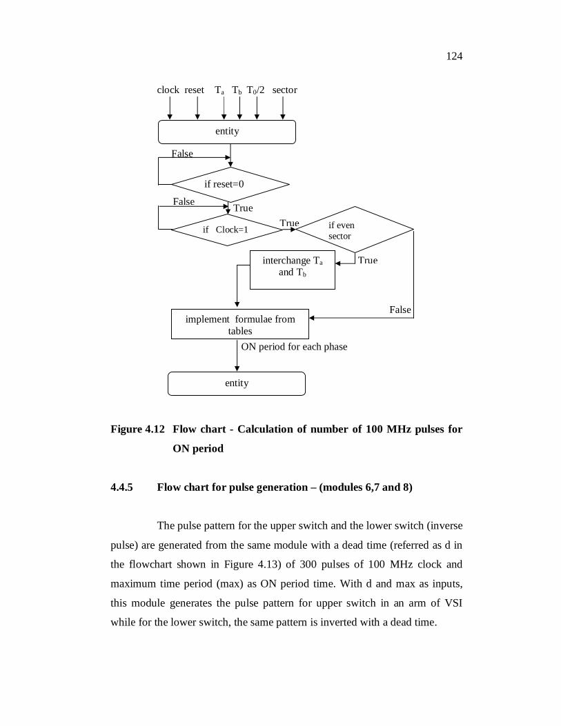
Figure 4.12 shows the flow chart for the calculation of number of
100 MHz pulses for ON period of each switch in each sector per phase.
124
entity
if reset=0
if Clock=1 if even sector
implement formulae from tables
interchange Taand Tb
entity
ON period for each phase
True
False
clock reset Ta Tb T0/2 sector
True True
False
False
Figure 4.12 Flow chart - Calculation of number of 100 MHz pulses for
ON period
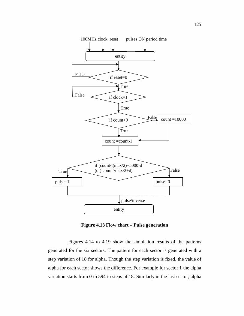
4.4.5 Flow chart for pulse generation – (modules 6,7 and 8)
The pulse pattern for the upper switch and the lower switch (inverse
pulse) are generated from the same module with a dead time (referred as d in
the flowchart shown in Figure 4.13) of 300 pulses of 100 MHz clock and
maximum time period (max) as ON period time. With d and max as inputs,
this module generates the pulse pattern for upper switch in an arm of VSI
while for the lower switch, the same pattern is inverted with a dead time.
125
100MHz clock reset pulses ON period time
entity
if reset=0
if clock=1
count =count-1
if count>0 count =10000
if (count<(max/2)+5000-d (or) count>max/2+d)
pulse=1 pulse=0
entity
True
True
False
False
True
False
True
pulse/inverse
False
Figure 4.13 Flow chart – Pulse generation
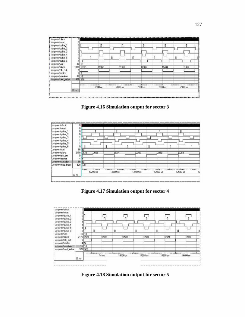
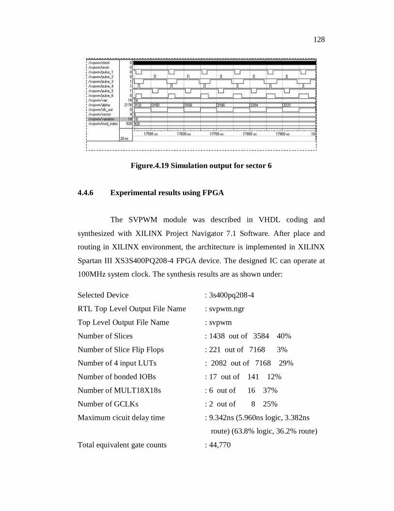
Figures 4.14 to 4.19 show the simulation results of the patterns
generated for the six sectors. The pattern for each sector is generated with a
step variation of 18 for alpha. Though the step variation is fixed, the value of
alpha for each sector shows the difference. For example for sector 1 the alpha
variation starts from 0 to 594 in steps of 18. Similarly in the last sector, alpha
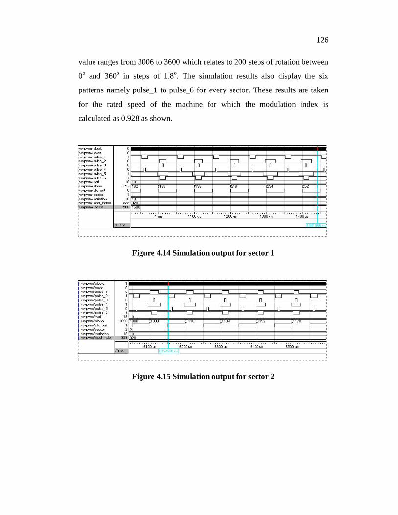
126
value ranges from 3006 to 3600 which relates to 200 steps of rotation between
0o and 360o in steps of 1.8o. The simulation results also display the six
patterns namely pulse_1 to pulse_6 for every sector. These results are taken
for the rated speed of the machine for which the modulation index is
calculated as 0.928 as shown.
Figure 4.14 Simulation output for sector 1
Figure 4.15 Simulation output for sector 2
127
Figure 4.16 Simulation output for sector 3
Figure 4.17 Simulation output for sector 4
Figure 4.18 Simulation output for sector 5
128
Figure.4.19 Simulation output for sector 6
4.4.6 Experimental results using FPGA
The SVPWM module was described in VHDL coding and
synthesized with XILINX Project Navigator 7.1 Software. After place and
routing in XILINX environment, the architecture is implemented in XILINX
Spartan III XS3S400PQ208-4 FPGA device. The designed IC can operate at
100MHz system clock. The synthesis results are as shown under:
Selected Device : 3s400pq208-4
RTL Top Level Output File Name : svpwm.ngr
Top Level Output File Name : svpwm
Number of Slices : 1438 out of 3584 40%
Number of Slice Flip Flops : 221 out of 7168 3%
Number of 4 input LUTs : 2082 out of 7168 29%
Number of bonded IOBs : 17 out of 141 12%
Number of MULT18X18s : 6 out of 16 37%
Number of GCLKs : 2 out of 8 25%
Maximum cicuit delay time : 9.342ns (5.960ns logic, 3.382ns
route) (63.8% logic, 36.2% route)
Total equivalent gate counts : 44,770

129
This realization is tested for its effectiveness by implementing it in
two stages. In the first stage, it is tested with a prototype PWM testing unit
and in the second stage, it is used to control the speed of a three phase
induction motor from 300 rpm to 1490 rpm.
4.4.6.1 First stage results (with prototype board)
SVPWM program module was downloaded from PC to FPGA
device using JTAG connectivity. The six PWM patterns from FPGA are given
to the base terminals of the transistors in the PWM testing unit. This testing
unit contains three phase R, L, C load connected to the output of six
transistors connected in bridge configuration each rated for 5 volts and 0.25
ampere. The outputs are observed using CRO and the Total Harmonic
Distortion (THD) is measured using LABVIEW software and BNC
connector. Figure 4.20 shows the photograph of the setup used for prototype
implementation.
Figure 4.20 Stage I setup with PWM testing unit
130
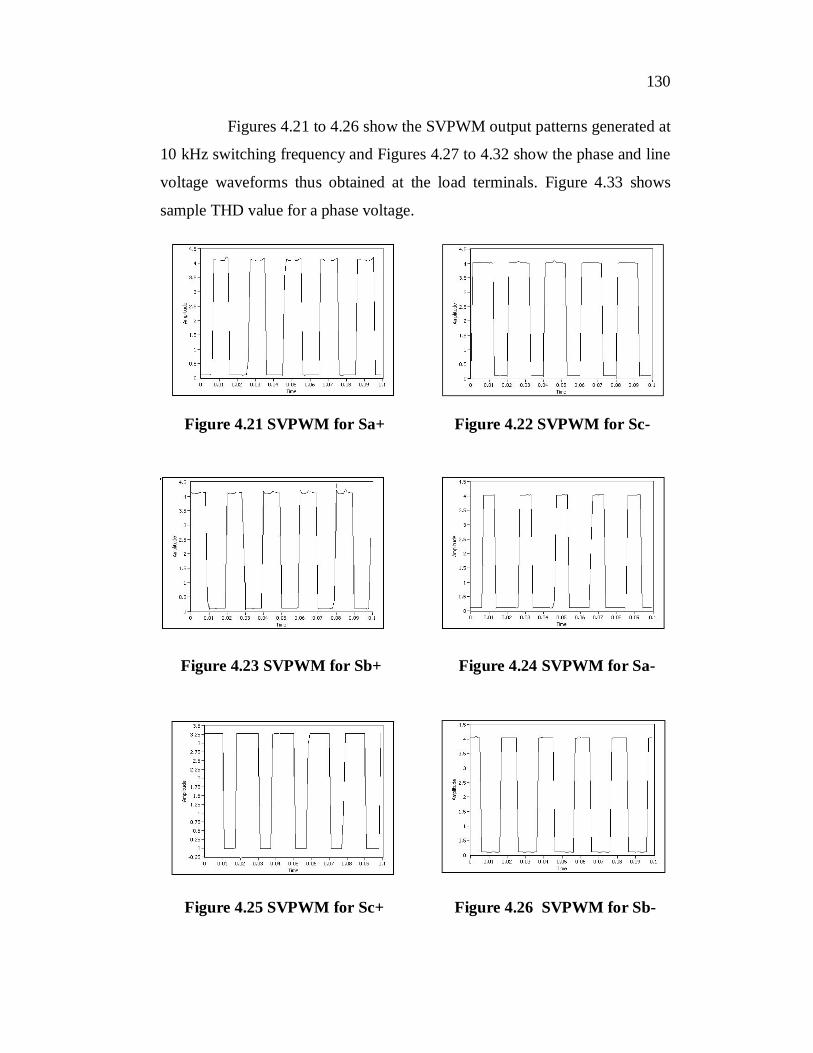
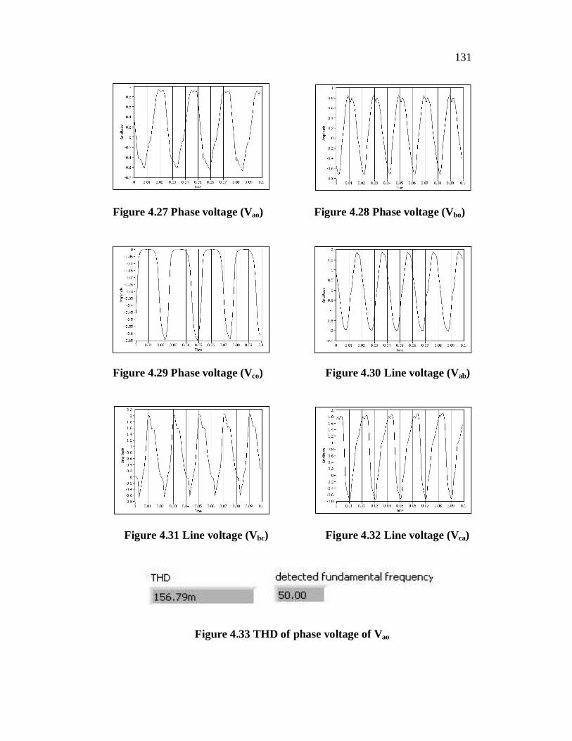
Figures 4.21 to 4.26 show the SVPWM output patterns generated at
10 kHz switching frequency and Figures 4.27 to 4.32 show the phase and line
voltage waveforms thus obtained at the load terminals. Figure 4.33 shows
sample THD value for a phase voltage.
Figure 4.21 SVPWM for Sa+ Figure 4.22 SVPWM for Sc-
Figure 4.23 SVPWM for Sb+ Figure 4.24 SVPWM for Sa-
Figure 4.25 SVPWM for Sc+ Figure 4.26 SVPWM for Sb-
131
Figure 4.27 Phase voltage (Vao) Figure 4.28 Phase voltage (Vbo)
Figure 4.29 Phase voltage (Vco) Figure 4.30 Line voltage (Vab)
Figure 4.31 Line voltage (Vbc) Figure 4.32 Line voltage (Vca)
Figure 4.33 THD of phase voltage of Vao
132
The waveforms shown in the Figures 4.21 to 4.33 are captured for
the near rated operation which depicts that the frequency is very close to 50
Hz. Also the amplitude is found to be very close to the rated value as for the
prototype board.
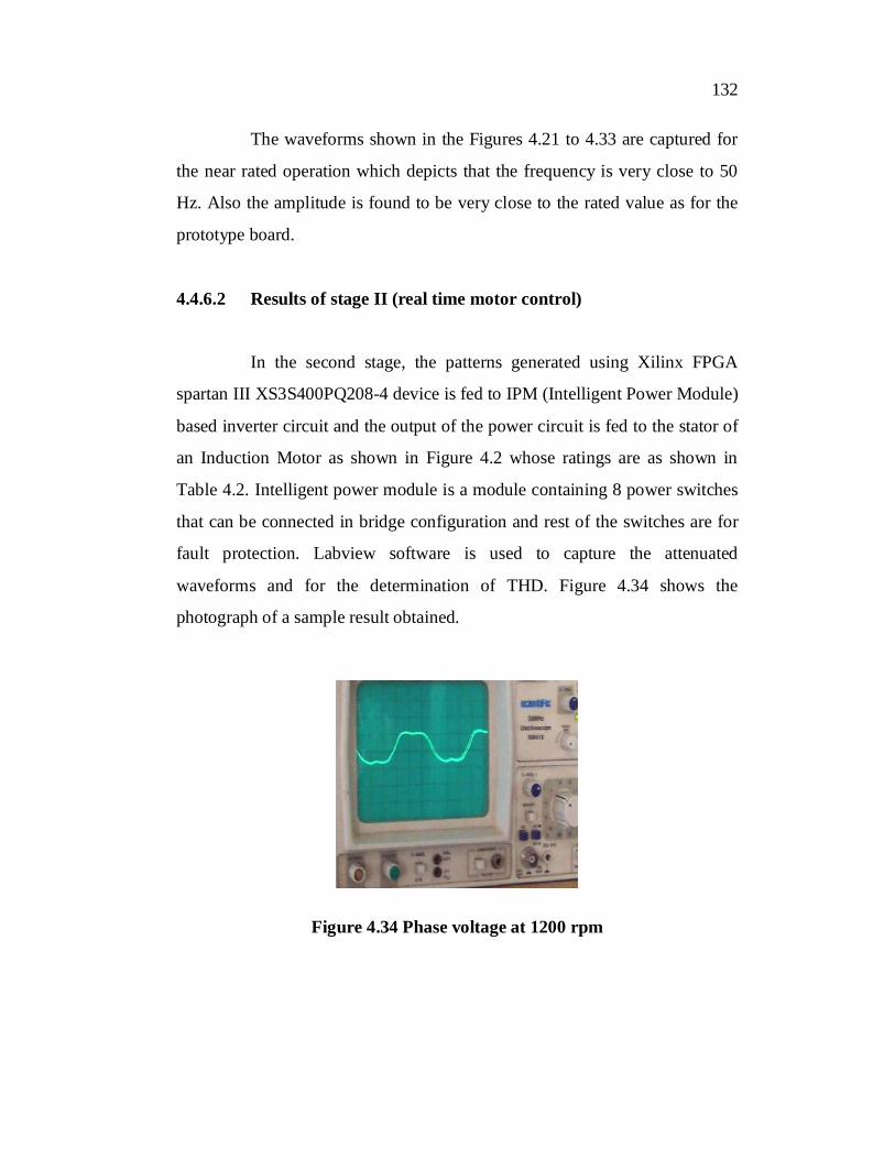
4.4.6.2 Results of stage II (real time motor control)
In the second stage, the patterns generated using Xilinx FPGA
spartan III XS3S400PQ208-4 device is fed to IPM (Intelligent Power Module)
based inverter circuit and the output of the power circuit is fed to the stator of
an Induction Motor as shown in Figure 4.2 whose ratings are as shown in
Table 4.2. Intelligent power module is a module containing 8 power switches
that can be connected in bridge configuration and rest of the switches are for
fault protection. Labview software is used to capture the attenuated
waveforms and for the determination of THD. Figure 4.34 shows the
photograph of a sample result obtained.
Figure 4.34 Phase voltage at 1200 rpm
133
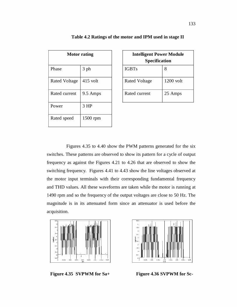
Table 4.2 Ratings of the motor and IPM used in stage II
Motor rating Intelligent Power Module Specification
Phase 3 ph IGBTs 8
Rated Voltage 415 volt Rated Voltage 1200 volt
Rated current 9.5 Amps Rated current 25 Amps
Power 3 HP
Rated speed 1500 rpm
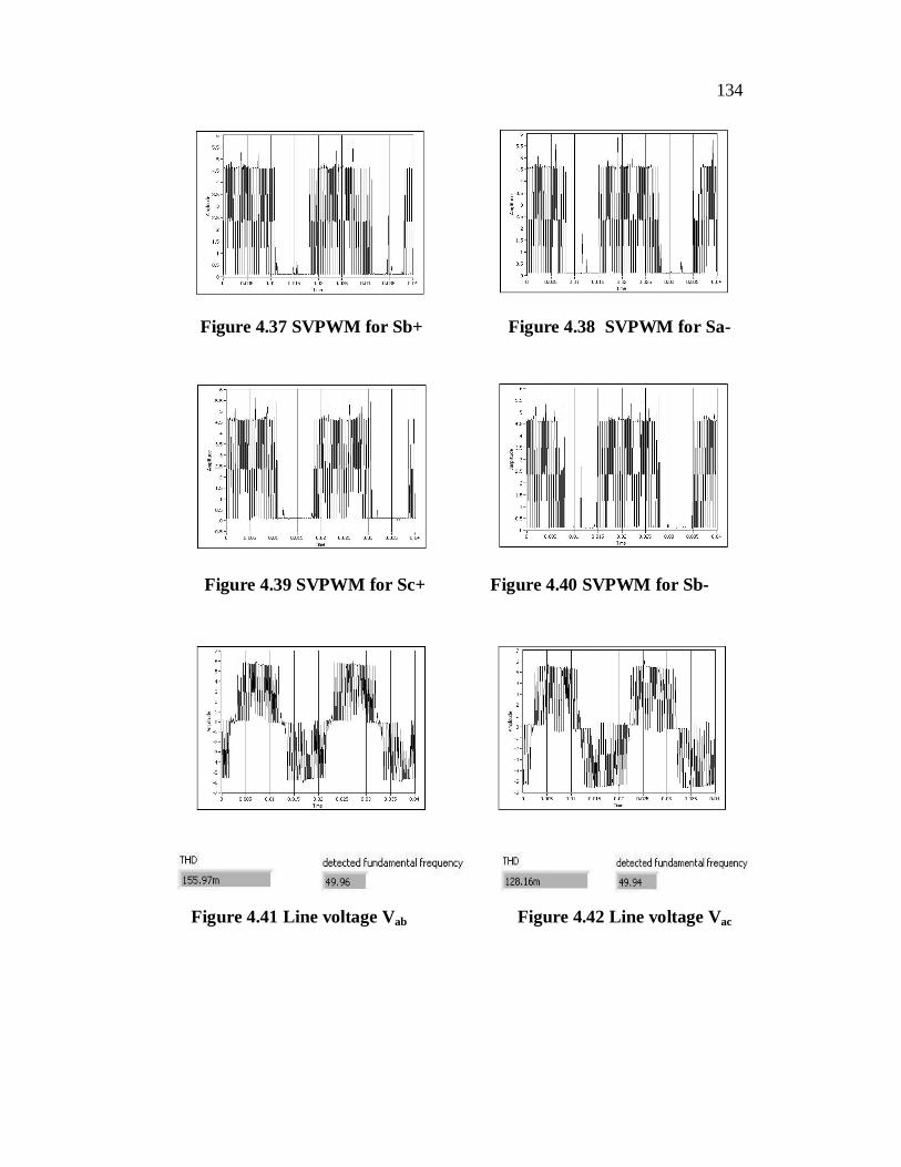
Figures 4.35 to 4.40 show the PWM patterns generated for the six
switches. These patterns are observed to show its pattern for a cycle of output
frequency as against the Figures 4.21 to 4.26 that are observed to show the
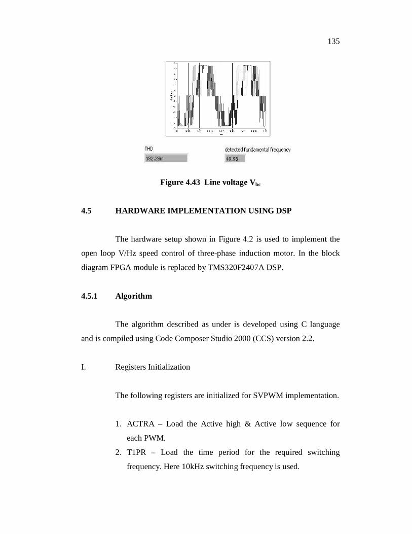
switching frequency. Figures 4.41 to 4.43 show the line voltages observed at
the motor input terminals with their corresponding fundamental frequency
and THD values. All these waveforms are taken while the motor is running at
1490 rpm and so the frequency of the output voltages are close to 50 Hz. The
magnitude is in its attenuated form since an attenuator is used before the
acquisition.
Figure 4.35 SVPWM for Sa+ Figure 4.36 SVPWM for Sc-
134
Figure 4.37 SVPWM for Sb+ Figure 4.38 SVPWM for Sa-
Figure 4.39 SVPWM for Sc+ Figure 4.40 SVPWM for Sb-
Figure 4.41 Line voltage Vab Figure 4.42 Line voltage Vac
135
Figure 4.43 Line voltage Vbc
4.5 HARDWARE IMPLEMENTATION USING DSP
The hardware setup shown in Figure 4.2 is used to implement the
open loop V/Hz speed control of three-phase induction motor. In the block
diagram FPGA module is replaced by TMS320F2407A DSP.
4.5.1 Algorithm
The algorithm described as under is developed using C language
and is compiled using Code Composer Studio 2000 (CCS) version 2.2.
I. Registers Initialization
The following registers are initialized for SVPWM implementation.
1. ACTRA – Load the Active high & Active low sequence for
each PWM.
2. T1PR – Load the time period for the required switching
frequency. Here 10kHz switching frequency is used.
136
Period value = ((CLK Frequency * PLL ratio) / (Prescaler *2)) /
(Desired Output Frequency)
3. T1CON – Select up/down counting mode, clock pre-scalar and
then enable timer.
4. DBTCONA – this is loaded with 6 micro seconds (Dead Band
Time).
5. COMCONA –This is the common control register and once
enabled, then all the PWM outputs are enabled as per the
ACTRA register.
II. Look Up Table Creation
As the TMS320F2407 DSP is a fixed point processor, the floating
point values are converted to the Q8 format. The sine value (Data)
for one full cycle is calculated as follows:
sine data for one cycle = Switching frequency / Output frequency
= (10000 / 50)
III. Speed Calculation
Based on the switch pressed in the DSP kit, the speed will be varied
by one rpm. Then the corresponding speed is stored as reference. If
the switch is not pressed, then old speed is maintained. The speed
range is from 300 rpm to 1490 rpm.
IV. ADC Routine
The ADC Routine is used to get the speed, three phase current
values if it exceeds the predetermined values and the fault PWM is
generated.
V. Sector Routine
1. From the reference speed, the modulation index and the output
frequency are calculated.
137
2. Data for one cycle based on the above calculation is chosen and
it is converted to one sector.
3. Ta, Tb and T0 values are calculated.
4. The sequencing is decided based on the ODD and EVEN
sectors and it is loaded to the compare registers with 50% DC
offset.
Here the SVPWM pattern is software determined and CCS 2000
compiler is used for compilation while in section 3.3.2 the pattern generation
is hardware determined.
4.5.2 Experimental results using DSP
The results are taken from two stages. First using the prototype –
PWM testing unit and the second is the real time implementation.
4.5.2.1 Stage I results
The C program developed for the algorithm explained in section
4.5.1 is compiled using CCS2000 to .out file and it is converted to .hex file
using the debugger tool before it is downloaded into the DSP. The six PWM
patterns from the DSP are given to the DSP testing unit specified in section
4.4.1.
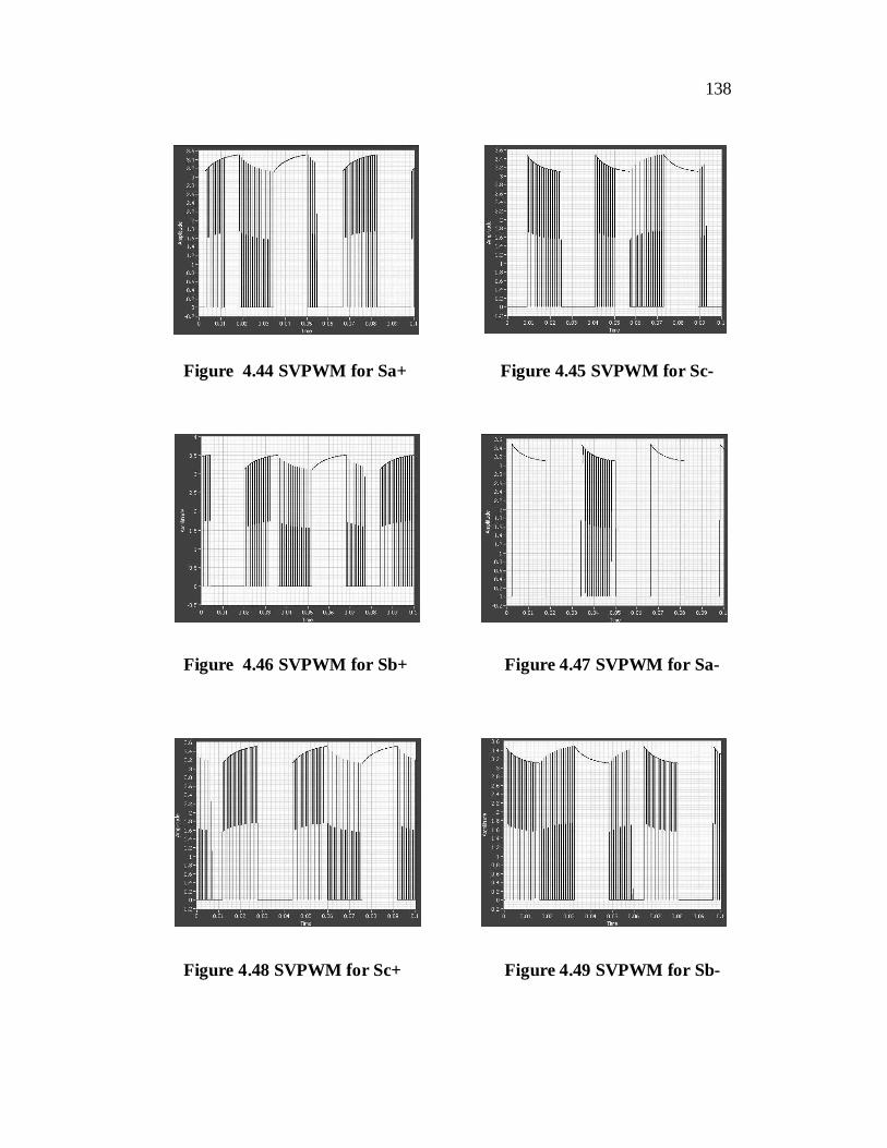
Figures 4.44 to 4.49 show the six SVPWM patterns generated at 10
kHz switching frequency. Figures 4.50 to 4.55 show the respective line and
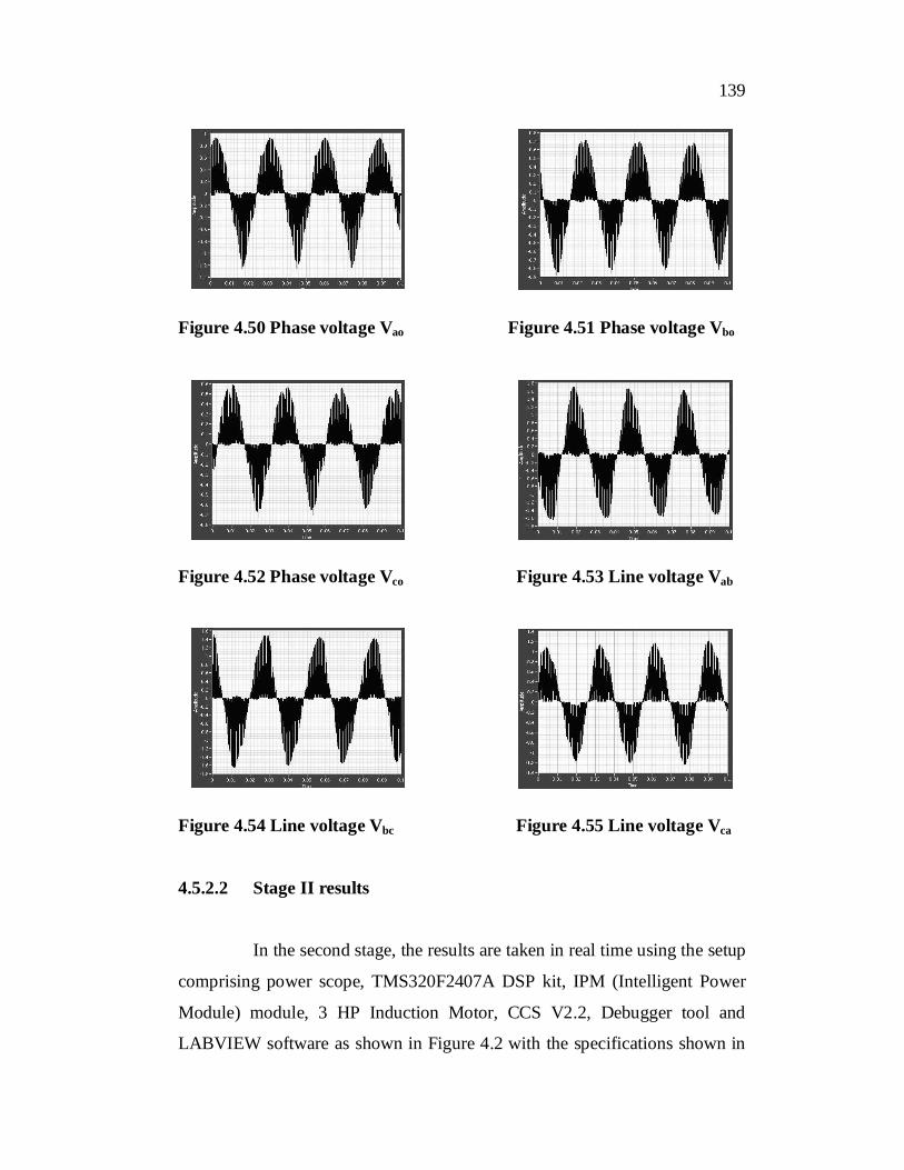
phase voltage waveforms observed at the load terminals.
138
Figure 4.44 SVPWM for Sa+ Figure 4.45 SVPWM for Sc-
Figure 4.46 SVPWM for Sb+ Figure 4.47 SVPWM for Sa-
Figure 4.48 SVPWM for Sc+ Figure 4.49 SVPWM for Sb-
139
Figure 4.50 Phase voltage Vao Figure 4.51 Phase voltage Vbo
Figure 4.52 Phase voltage Vco Figure 4.53 Line voltage Vab
Figure 4.54 Line voltage Vbc Figure 4.55 Line voltage Vca
4.5.2.2 Stage II results
In the second stage, the results are taken in real time using the setup
comprising power scope, TMS320F2407A DSP kit, IPM (Intelligent Power
Module) module, 3 HP Induction Motor, CCS V2.2, Debugger tool and
LABVIEW software as shown in Figure 4.2 with the specifications shown in

140
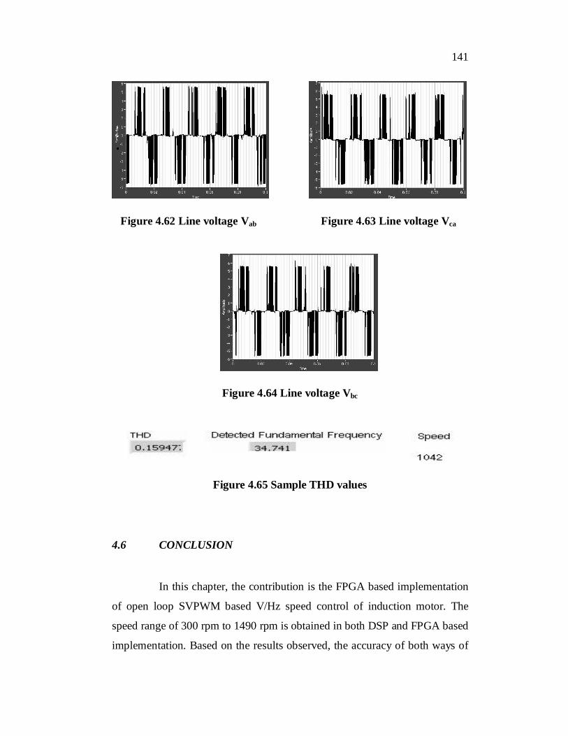
Table 4.2. Figures 4.56 to 4.61 show the six SVPWM patterns, Figures 4.62
to 4.64 show the corresponding line voltage waveforms obtained at a rated
speed. Figure 4.65 shows the sample THD value obtained at a speed of 1042
rpm and its corresponding fundamental frequency.
Figure 4.56 SVPWM for Sa+ Figure 4.57 SVPWM for Sc-
Figure 4.58 SVPWM for Sb+ Figure 4.59 SVPWM for Sa-
Figure 4.60 SVPWM for Sc+ Figure 4.61 SVPWM for Sb-
141
Figure 4.62 Line voltage Vab Figure 4.63 Line voltage Vca
Figure 4.64 Line voltage Vbc
Figure 4.65 Sample THD values
4.6 CONCLUSION
In this chapter, the contribution is the FPGA based implementation
of open loop SVPWM based V/Hz speed control of induction motor. The
speed range of 300 rpm to 1490 rpm is obtained in both DSP and FPGA based
implementation. Based on the results observed, the accuracy of both ways of
142
implementation is same. THD values justify this. And the major advantage of
FPGA based implementation is its speed of execution. It is only 9.342 ns. The
algorithm is realized as architecture in FPGA while with DSP it is still a
sequential execution of the instructions which takes the CPU overhead time in
microseconds. In addition, the reconfigurable structure of the FPGA gives an
optimization in the space requirement. This successful attempt triggers to use
FPGAs for high performance controller realization.