chapter 2b: switch-level modeling - wiley.com · chapter 2: structural modeling digital system...
TRANSCRIPT
Chapter 2: Structural Modeling
Digital System Designs and Practices Using Verilog HDL and FPGAs @ 2008~2010, John Wiley 2-1
Chapter 2b: Switch-Level Modeling
Department of Electronic Engineering
National Taiwan University of Science and Technology
Prof. Ming-Bo Lin
Chapter 2: Structural Modeling
Digital System Designs and Practices Using Verilog HDL and FPGAs @ 2008~2010, John Wiley 2-2
Syllabus
ObjectivesSwitch primitivesDelay specificationsSignal strengths
Chapter 2: Structural Modeling
Digital System Designs and Practices Using Verilog HDL and FPGAs @ 2008~2010, John Wiley 2-3
Objectives
After completing this chapter, you will be able toDescribe what is the structural modelingDescribe how to instantiate switch primitivesDescribe how to model a design in switch primitivesDescribe how to specify delays in switchesDescribe other features of switch primitives
Chapter 2: Structural Modeling
Digital System Designs and Practices Using Verilog HDL and FPGAs @ 2008~2010, John Wiley 2-4
Syllabus
ObjectivesSwitch primitives
MOS switchesCMOS switchBidirectional switches
Delay specificationsSignal strengths
Chapter 2: Structural Modeling
Digital System Designs and Practices Using Verilog HDL and FPGAs @ 2008~2010, John Wiley 2-5
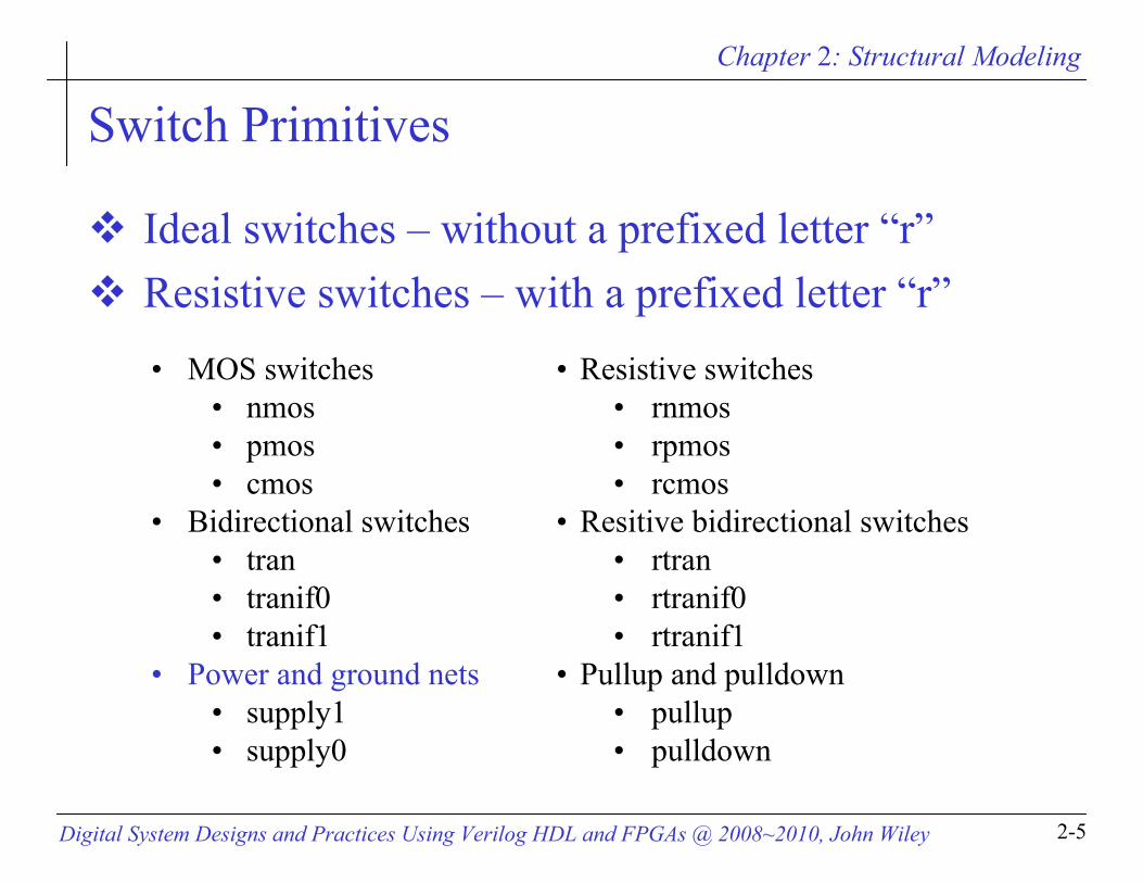
Switch Primitives
Ideal switches – without a prefixed letter “r”Resistive switches – with a prefixed letter “r”• MOS switches
• nmos• pmos• cmos
• Bidirectional switches• tran• tranif0• tranif1
• Power and ground nets• supply1 • supply0
• Resistive switches• rnmos• rpmos• rcmos
• Resitive bidirectional switches• rtran• rtranif0• rtranif1
• Pullup and pulldown• pullup• pulldown
Chapter 2: Structural Modeling
Digital System Designs and Practices Using Verilog HDL and FPGAs @ 2008~2010, John Wiley 2-6
Syllabus
ObjectivesSwitch primitives
MOS switchesCMOS switchBidirectional switches
Delay specificationsSignal strengths
Chapter 2: Structural Modeling
Digital System Designs and Practices Using Verilog HDL and FPGAs @ 2008~2010, John Wiley 2-7
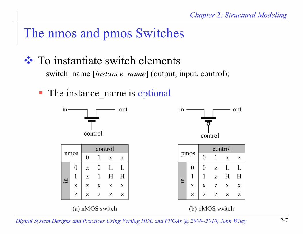
The nmos and pmos Switches
To instantiate switch elements
The instance_name is optional
switch_name [instance_name] (output, input, control);
Chapter 2: Structural Modeling
Digital System Designs and Practices Using Verilog HDL and FPGAs @ 2008~2010, John Wiley 2-8
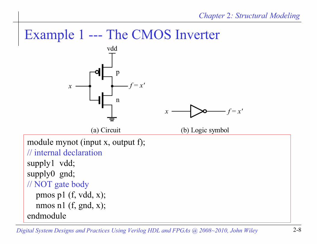
Example 1 --- The CMOS Inverter
module mynot (input x, output f);// internal declarationsupply1 vdd;supply0 gnd;// NOT gate body
pmos p1 (f, vdd, x); nmos n1 (f, gnd, x);
endmodule
Chapter 2: Structural Modeling
Digital System Designs and Practices Using Verilog HDL and FPGAs @ 2008~2010, John Wiley 2-9
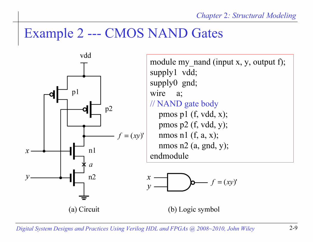
Example 2 --- CMOS NAND Gates
module my_nand (input x, y, output f);supply1 vdd;supply0 gnd;wire a; // NAND gate body
pmos p1 (f, vdd, x); pmos p2 (f, vdd, y); nmos n1 (f, a, x); nmos n2 (a, gnd, y);
endmodule
Chapter 2: Structural Modeling
Digital System Designs and Practices Using Verilog HDL and FPGAs @ 2008~2010, John Wiley 2-10
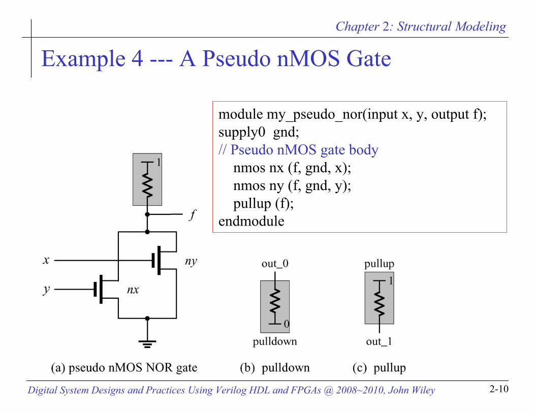
Example 4 --- A Pseudo nMOS Gate
module my_pseudo_nor(input x, y, output f);supply0 gnd;// Pseudo nMOS gate body
nmos nx (f, gnd, x); nmos ny (f, gnd, y); pullup (f);
endmodule
Chapter 2: Structural Modeling
Digital System Designs and Practices Using Verilog HDL and FPGAs @ 2008~2010, John Wiley 2-11
Syllabus
ObjectivesSwitch primitives
MOS switchesCMOS switchBidirectional switches
Delay specificationsSignal strengths
Chapter 2: Structural Modeling
Digital System Designs and Practices Using Verilog HDL and FPGAs @ 2008~2010, John Wiley 2-12
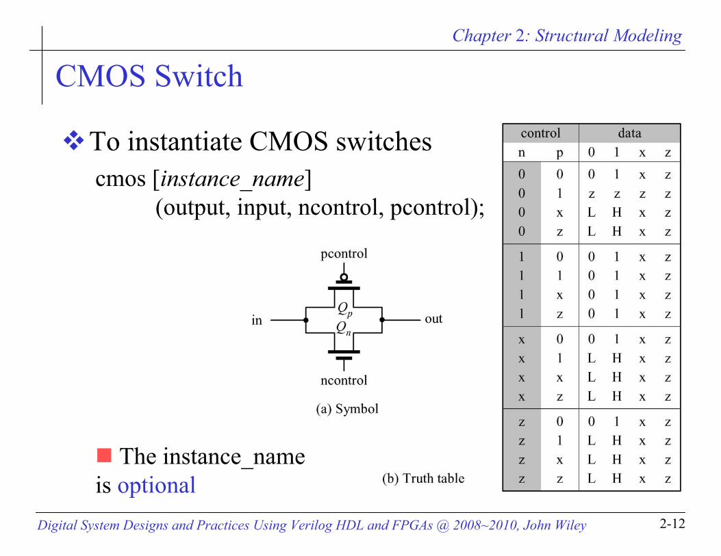
CMOS Switch
The instance_nameis optional
To instantiate CMOS switchescmos [instance_name]
(output, input, ncontrol, pcontrol);
Chapter 2: Structural Modeling
Digital System Designs and Practices Using Verilog HDL and FPGAs @ 2008~2010, John Wiley 2-13
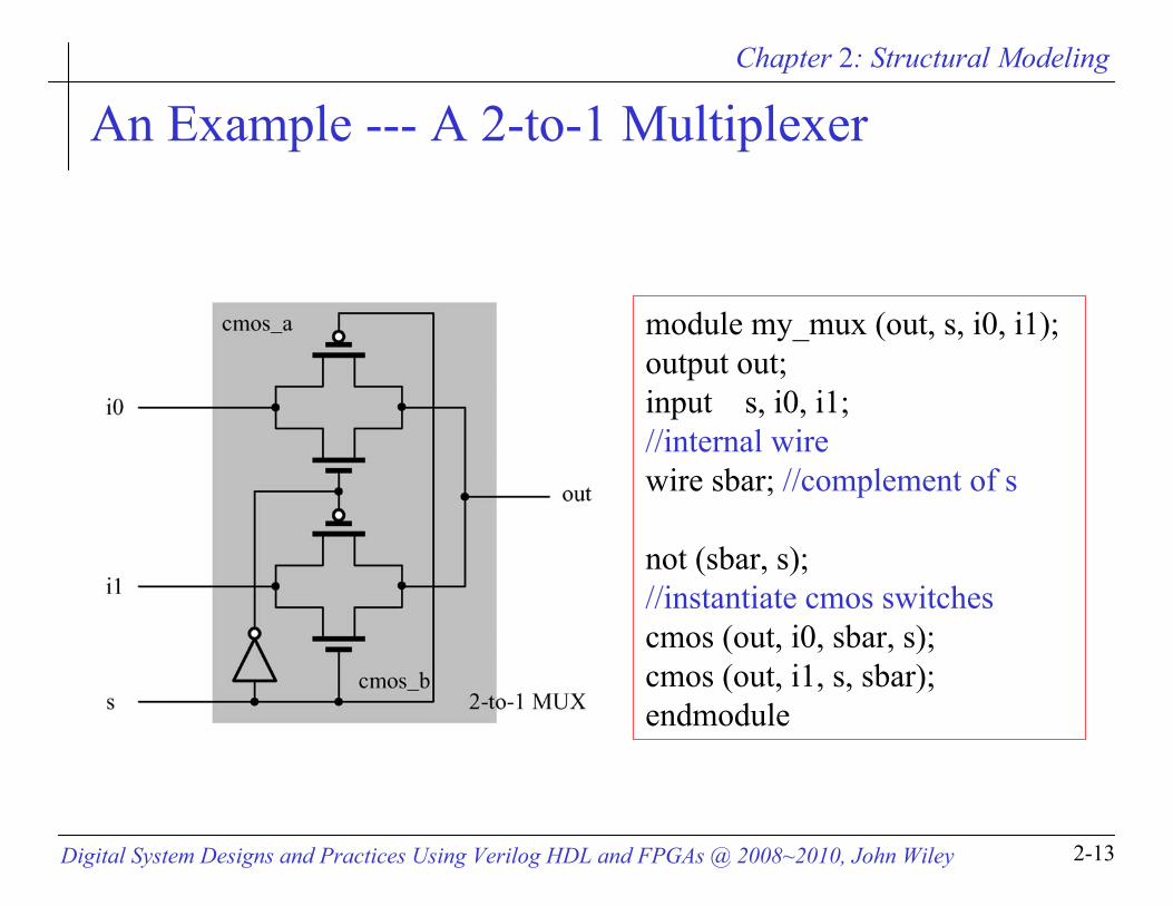
An Example --- A 2-to-1 Multiplexer
module my_mux (out, s, i0, i1);output out;input s, i0, i1;//internal wirewire sbar; //complement of s
not (sbar, s); //instantiate cmos switchescmos (out, i0, sbar, s);cmos (out, i1, s, sbar);endmodule
Chapter 2: Structural Modeling
Digital System Designs and Practices Using Verilog HDL and FPGAs @ 2008~2010, John Wiley 2-14
Syllabus
ObjectivesSwitch primitives
MOS switchesCMOS switchBidirectional switches
Delay specificationsSignal strengths
Chapter 2: Structural Modeling
Digital System Designs and Practices Using Verilog HDL and FPGAs @ 2008~2010, John Wiley 2-15
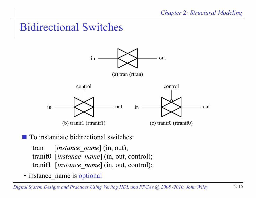
Bidirectional Switches
• instance_name is optional
To instantiate bidirectional switches:tran [instance_name] (in, out);tranif0 [instance_name] (in, out, control);tranif1 [instance_name] (in, out, control);
Chapter 2: Structural Modeling
Digital System Designs and Practices Using Verilog HDL and FPGAs @ 2008~2010, John Wiley 2-16
Syllabus
ObjectivesSwitch primitivesDelay specifications
MOS/CMOS switchesBidirectional switches
Signal strengths
Chapter 2: Structural Modeling
Digital System Designs and Practices Using Verilog HDL and FPGAs @ 2008~2010, John Wiley 2-17
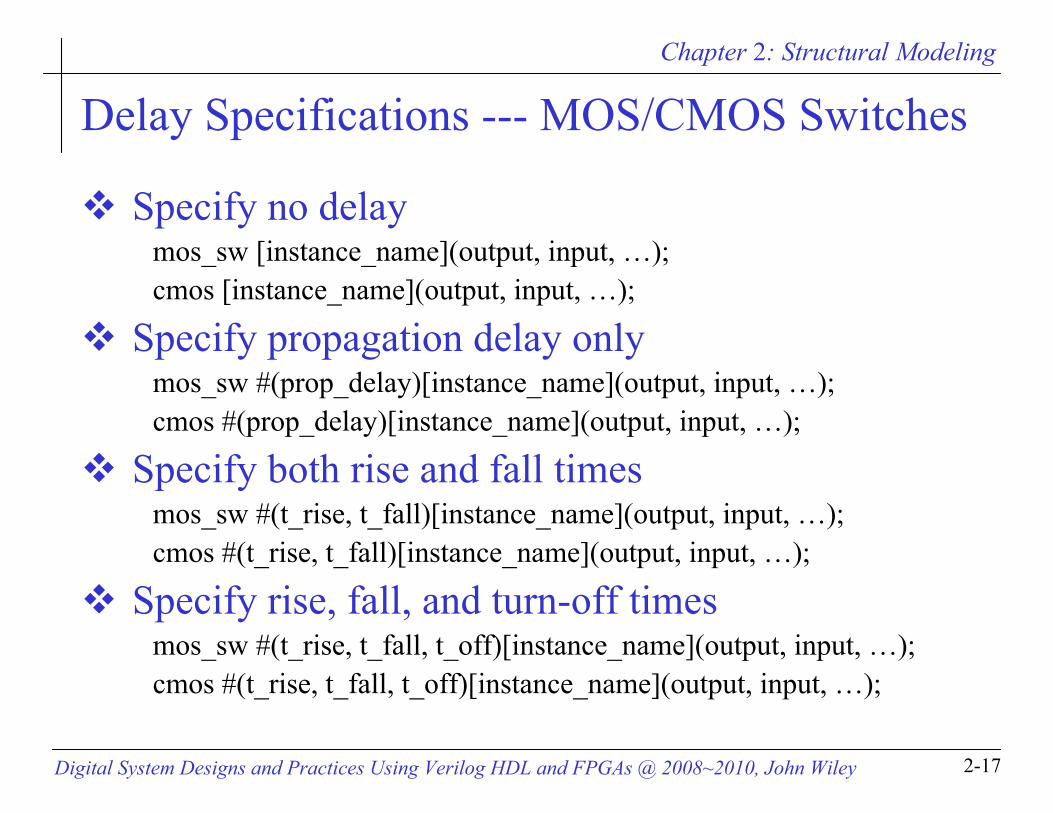
Delay Specifications --- MOS/CMOS Switches
Specify no delaymos_sw [instance_name](output, input, …);cmos [instance_name](output, input, …);
Specify propagation delay onlymos_sw #(prop_delay)[instance_name](output, input, …);cmos #(prop_delay)[instance_name](output, input, …);
Specify both rise and fall timesmos_sw #(t_rise, t_fall)[instance_name](output, input, …);cmos #(t_rise, t_fall)[instance_name](output, input, …);
Specify rise, fall, and turn-off timesmos_sw #(t_rise, t_fall, t_off)[instance_name](output, input, …);cmos #(t_rise, t_fall, t_off)[instance_name](output, input, …);
Chapter 2: Structural Modeling
Digital System Designs and Practices Using Verilog HDL and FPGAs @ 2008~2010, John Wiley 2-18
Syllabus
ObjectivesSwitch primitivesDelay specifications
MOS/CMOS switchesBidirectional switches
Signal strengths
Chapter 2: Structural Modeling
Digital System Designs and Practices Using Verilog HDL and FPGAs @ 2008~2010, John Wiley 2-19
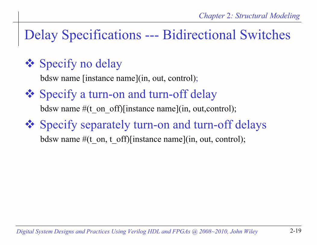
Delay Specifications --- Bidirectional Switches
Specify no delaybdsw name [instance name](in, out, control);
Specify a turn-on and turn-off delaybdsw name #(t_on_off)[instance name](in, out,control);
Specify separately turn-on and turn-off delaysbdsw name #(t_on, t_off)[instance name](in, out, control);
Chapter 2: Structural Modeling
Digital System Designs and Practices Using Verilog HDL and FPGAs @ 2008~2010, John Wiley 2-20
Syllabus
ObjectivesSwitch primitivesDelay specificationsSignal strengths
Signal strengthstrireg examples
Chapter 2: Structural Modeling
Digital System Designs and Practices Using Verilog HDL and FPGAs @ 2008~2010, John Wiley 2-21
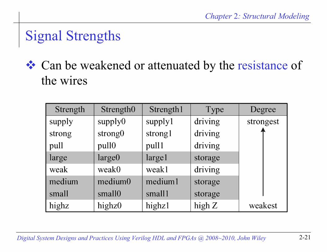
Signal Strengths
Can be weakened or attenuated by the resistance of the wires
Chapter 2: Structural Modeling
Digital System Designs and Practices Using Verilog HDL and FPGAs @ 2008~2010, John Wiley 2-22
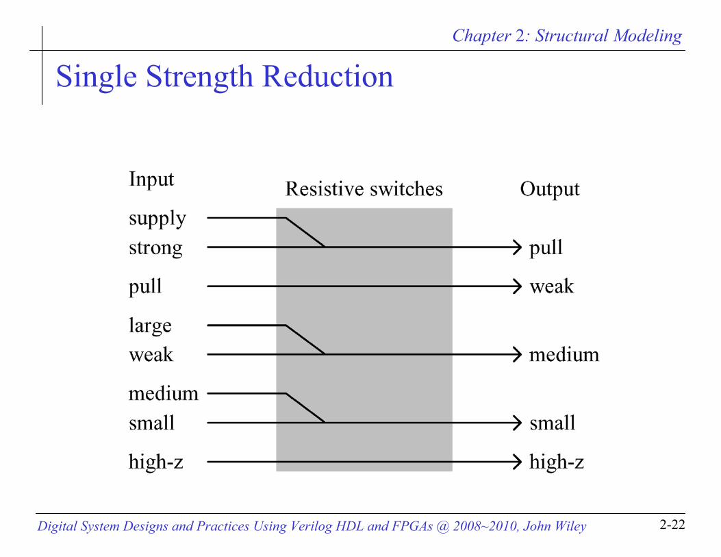
Single Strength Reduction
Chapter 2: Structural Modeling
Digital System Designs and Practices Using Verilog HDL and FPGAs @ 2008~2010, John Wiley 2-23
Syllabus
ObjectivesSwitch primitivesDelay specificationsSignal strengths
Signal strengthstrireg nets
Chapter 2: Structural Modeling
Digital System Designs and Practices Using Verilog HDL and FPGAs @ 2008~2010, John Wiley 2-24
trireg Nets
Driven stateCapacitive state
Chapter 2: Structural Modeling
Digital System Designs and Practices Using Verilog HDL and FPGAs @ 2008~2010, John Wiley 2-25
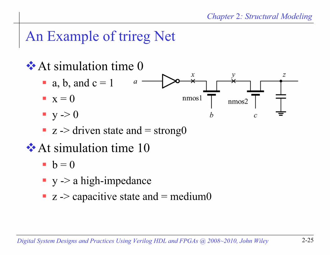
An Example of trireg Net
At simulation time 0a, b, and c = 1x = 0y -> 0 z -> driven state and = strong0
At simulation time 10 b = 0y -> a high-impedance z -> capacitive state and = medium0
Chapter 2: Structural Modeling
Digital System Designs and Practices Using Verilog HDL and FPGAs @ 2008~2010, John Wiley 2-26
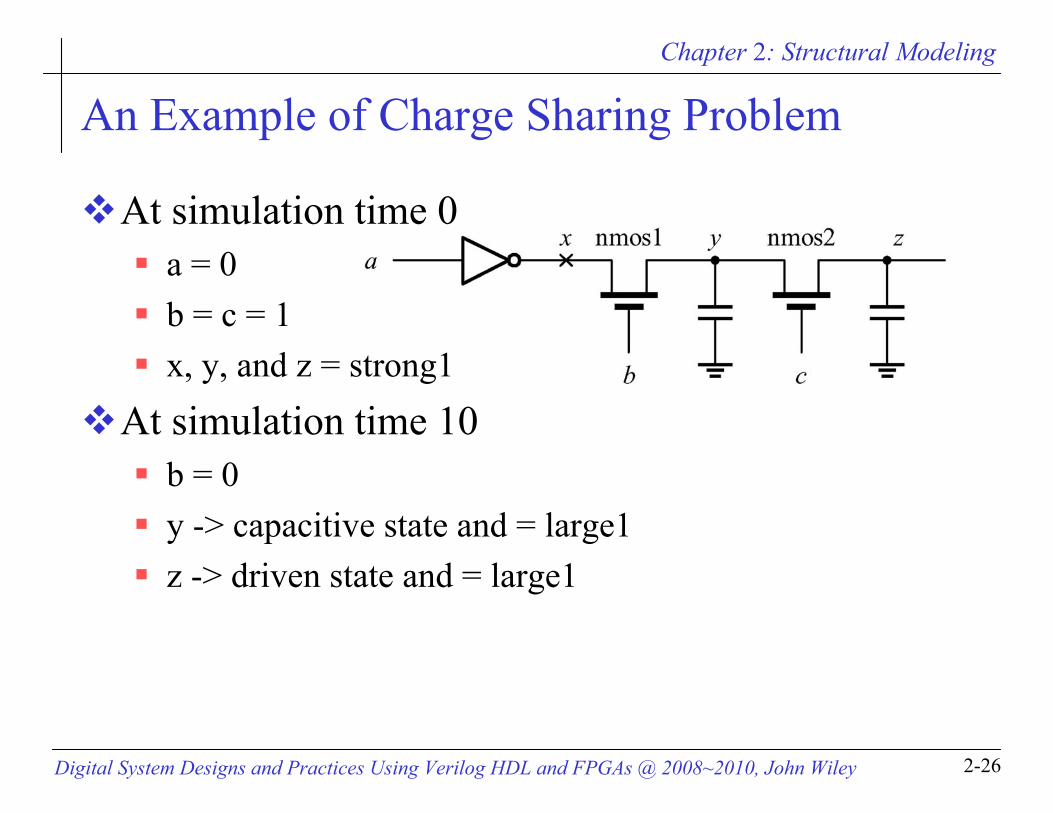
An Example of Charge Sharing Problem
At simulation time 0a = 0b = c = 1x, y, and z = strong1
At simulation time 10 b = 0y -> capacitive state and = large1 z -> driven state and = large1
Chapter 2: Structural Modeling
Digital System Designs and Practices Using Verilog HDL and FPGAs @ 2008~2010, John Wiley 2-27
An Example of Charge Sharing Problem
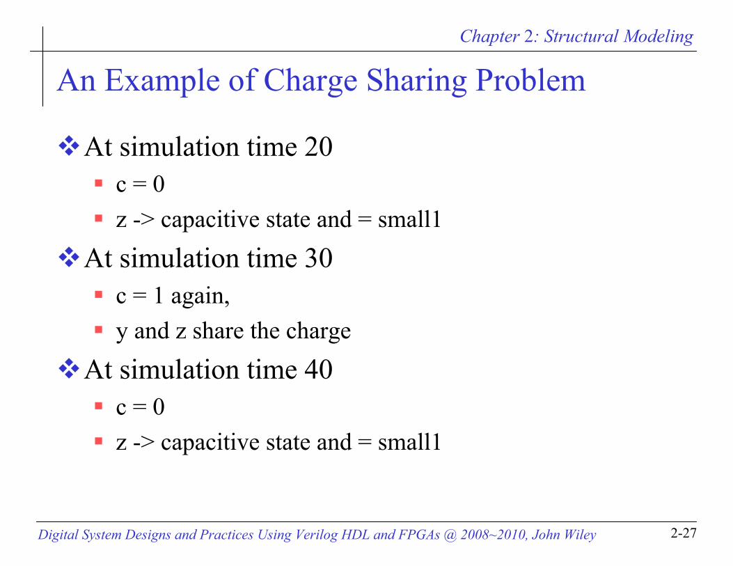
At simulation time 20 c = 0z -> capacitive state and = small1
At simulation time 30 c = 1 again, y and z share the charge
At simulation time 40 c = 0 z -> capacitive state and = small1