chapter 2 - synchronous rectification · in a continuing effort to increase the density and speed...
TRANSCRIPT

2. Synchronous Rectification 9
2 SYNCHRONOUS RECTIFICATION
Chapter Two
Synchronous Rectification
The conduction loss of diode rectifier contributes significantly to the overall power loss in
a power supply, especially in low output-voltage applications. The rectifier conduction loss is
proportional to the product of its forward-voltage drop, VF, and the forward conduction current,
IF. On the other hand, operating in the MOSFET III quadrant, a synchronous rectifier presents a
resistive i-v characteristics, as shown in Fig. 2.1. Under certain current level, the forward-voltage
drop of a synchronous rectifier can be lower than that of a diode rectifier, and consequently
reduces the rectifier conduction loss [A1]. Due to the fact that synchronous rectifiers are active
devices, the design and utilization of synchronous rectification need to be properly addressed.
This chapter analyzes the application of synchronous rectification in two most popular
isolated topologies, forward and flyback converters. The limits of efficiency improvements that
can be obtained using synchronous rectification are determined. Conversion efficiencies of
different implementations are compared, and verified with experimental evaluations.

2. Synchronous Rectification 10
0 0.1 0.2 0.3 0.4 0.5 0.6 0.7
V [V]
0
10
20
30
40
50
I [A
]
Synchronous Rectifier
Diode Rectifier
F
F
Figure 2.1. Forward-voltage comparison between synchronous rectifier and diode rectifier. area has conduction loss saving by using synchronous rectifiers.

2. Synchronous Rectification 11
2.1. Synchronous Rectification in Forward Converter
In a continuing effort to increase the density and speed and to decrease power
consumption of data-processing circuits, their power supply requirements are being reduced from
5V to 3.3V. The increased availability and use of 3.3-V logic ICs have spurred significant
development and research efforts in the area of low-voltage power supplies. A number of
approaches with different goals and levels of complexity have been taken in these designs. They
range from simple dc/dc buck-converter add-on modules that convert outputs of existing power
supplies to the modules that convert outputs of existing power supplies to the required low
voltage, to more sophisticated ac/dc converters with synchronous rectifiers (SRs).
A number of SR implementations have been described so far [A2-A14]. Based on the
method employed in driving SRs, all of them can be classified into two groups: control-driven
and self-driven. In a control-driven SR implementation, the SRs are driven by gate-drive signals
derived from the gate-drive of the main switch. In a self-driven SR implementation, the SRs are
driven directly with the secondary voltage of the transformer. As a result, the self-driven SR
approach is very attractive since it is simple and requires a minimum number of components.
However, the performance of self-driven SRs depends on the resetting method of the
power transformer since the freewheeling synchronous rectifier is driven by the reset voltage.

2. Synchronous Rectification 12
Ideally, it would be desirable that the resetting time be equal to the off-time of the primary switch.
Then the output current would freewheel through the SR for the entire off (freewheeling) time.
The objective of this section is twofold. The first is to theoretically determine the limit of
efficiency improvements that can be obtained form SRs. This limit is primarily a function of the
output voltage, output current, on-resistance of the SR, and the forward-voltage drop of Schottky
rectifiers replaced by SRs. The second objective is to compare conversion efficiencies of control-
driven SRs with those of different self-driven SR implementations. Specifically, performance
comparisons of the forward converters with RCD-clamp and active-clamp reset are made.
2.1.1. Synchronous Rectifier Implementations
A. Forward Converter with RCD Clamp and Self-Driven SRs
The forward converter with self-driven SRs and its key waveforms are shown in Fig. 2.2.
In this circuit, synchronous rectifiers SR2 (Q2 and D2) and SR3 (Q3 and D3) are crosscoupled to the
secondary winding of the transformer and are directly driven by the secondary voltage. Since no
driver or control circuit is used to provide the gate-drive signals, this implementation of
synchronous rectification is the simplest possible. However, its performance is strongly
dependent on the method of the transformer core resetting, because the gate-drive signal for
synchronous rectifier SR3 is derived from the reset voltage.

2. Synchronous Rectification 13
Vin
+
-VC
S
Vs
+
-
D3
D2
Q2
Q3
Ion:1
Cs
Ip
Tdead
VsVinn
VGS
VDS
Vin
I D2
IQ2
Q2 D2
ID3
IQ3
Q3 D3D3
Son
T s
VC
Vth2
Vth3
VGS2
VGS3
Qrr
Im-D2
Tcomon
Tcomoff
(b)
(c)
(f)
(d)
(e)
(a)
D2
I - Io m-
Figure 2.2. Forward converter with RCD clamp and self-driven SRs: (a) circuit diagram, (b)gate-drive signal, (c) drain-to-source voltage of primary switch, (d) secondarywinding voltage, (e) current through SR2, and (f) current through SR3. Cs
represents total capacitance seen at drain of MOSFET. Note that, for clarity,commutation times Tcom
on and Tcomoff are shown exaggerated.

2. Synchronous Rectification 14
As can be seen from the waveform in Fig. 2.2(e), once the transformer reset is completed,
the magnetizing current of the transformer, Im− , starts flowing through the body diode of SR2
[A17]. The magnitude of this current is given by [A17]:
I NV
L CmC
m s
− =/
(2-1)
where N is the turns ratio of the transformer, VC is the transformer reset voltage, Lm is
magnetizing inductance of the transformer, and Cs is the total capacitance seen at the drain of the
primary switch. This capacitance is the sum of the output capacitance of the primary switch
(Coss), winding capacitance of the transformer (Ctr), the clamp-diode junction capacitance(CD),
reflected input capacitance of SR3 (C NissQ3 2/ ), and reflected output capacitance of SR2
(C NossQ2 2/ ).
Also, as can be seen from the waveforms in Fig. 2.2(f), after the transformer reset is
completed, the difference between load current Io and magnetizing current Im− is diverted from
transistor Q3 to the body diode, D3, of SR3. Due to relatively high forward-voltage drops of the
body diodes of SR2 and SR3, the efficiency of synchronous rectification is reduced. The efficiency
loss due to the body-diode conduction depends on the duration of the dead time (Tdead) and the
forward-voltage drops of the body diodes (VBD). This loss can be minimized by connecting
Schottky diodes in parallel with SR2 and/or SR3 or by minimizing the conduction times of D2 and
D3. While the conduction time of D3 can be minimized either by driving Q3 by an external gate-
drive signal or by minimizing the dead time by employing a different reset scheme [A9, A18], the

2. Synchronous Rectification 15
conduction time of D2 can be shortened only by employing a transformer reset scheme that
minimizes the dead time, as will be discussed in more detail in the following subsections.
However, it should be noted that for load currents much greater than magnetizing current Im− , the
efficiency loss occurring during the dead time due to the conduction of D3 is much greater than
that of D2. Since for properly designed converter Im− is usually less than 2A, the effect of D2
conduction loss due to Im− on the efficiency is relatively small at output currents exceeding 15 to
20 A.
The conduction losses of the body diodes of SR2 and SR3 are also dependent on the
commutation time Tcomon and Tcom
off shown in Figs. 2.2(e) and 2.2(f). In fact, the body diode of SR2,
D2, conducts only during a brief period immediately after the primary switch is turned off and
during the dead time. While the dead time is solely determined by the transformer reset voltage,
the commutation time of D2 after the turn-off of the primary switch depends on the fall time of
the secondary voltage (see Fig 2.2(d)) and the commutation time (Tcomoff ) of the output current
from diode D2 to transistor Q3. Commutation time Tcomoff is dependent on the secondary-side
inductance that consists of the leakage inductance of the transformer, the packaging inductance
of the SRs, and the secondary-side interconnect inductance. The secondary-side inductance also
determines the commutation time(Tcomon ) which is required to commutate current from diode D3
to transistor Q2 after the primary switch is turned on. Since for output current Io >> Im− , the
conduction loss of body diode D3 during the dead time is much higher than the corresponding
conduction loss of D2. As a result, the conduction loss of D2 during commutation time Tcomoff has a

2. Synchronous Rectification 16
much stronger effect on the total conduction loss of SR2 compared to the effect that the
conduction loss of D3 during commutation time Tcomon has on the total loss of SR3. To minimize
the commutation times, the total inductance of the secondary side should be minimized.
Moreover, it is especially important to make the leakage inductance of the transformer small
relative to the other circuit inductance to avoid a loss of gate-drive voltage for SRs as explained in
[A7].
Finally, it should be noted that the conduction of the body diodes of SRs not only
increases the conduction loss, but also introduces the power loss due to their reverse recovery.
This loss, which appears on the body diode and the transistor of the opposite SR during the diode
turn-off, is proportional to the recovered charge Qrr indicated in Figs. 2.2(e) and 2.2(f), frequency,
and secondary voltage [A20]. Therefore, it is relatively significant at full load and high line. The
only method of eliminating this loss is to parallel the Schottky diodes to SR2 and SR3.
B. Forward Converter with Active Clamp and Self-Driven SRs
The forward converter with active-clamp reset and its key waveforms are shown in Fig.
2.3. As can be seen, the active-clamp-reset approach minimizes the duration of the dead time
since the transformer core is reset during almost the entire off time of the primary switch [A18,
A19]. As a result, the conduction time of transistor Q3 is maximized, the time during which D2 is
conducting magnetizing current is minimized. Consequently, the conversion efficiency of the
converter with the active-clamp reset is improved relative to the RCD-clamp counterpart. Also,
the active-clamp reset approach minimizes voltage stress on the primary switch. In addition, the
primary switch in this circuit can be turned on at zero voltage by properly adjusting the

2. Synchronous Rectification 17
Vin
+
-VC
S
Vs
+
-D3
D2
SR2
SR3
Ion:1
Cs
Ip
Tdelay
VsVinn
VGS
VDS
Vin
ID2
IQ2
Q2D2
ID3
IQ3
Q3
Son
VC
Vth2
Vth3
VGS2
VGS3
Qrr
D2
(b)
(c)
(f)
(d)
(e)
(a)
S1
S1on
D3D3
Figure 2.3. Forward converter with active-clamp and self-driven SRs: (a) circuit diagram, (b)gate-drive signals, (c) drain-to-source voltage of primary switch, (d) secondarywinding voltage, (e) current through SR2, and (f) current through SR3.
Tdead

2. Synchronous Rectification 18
magnetizing inductance of the transformer [A16]. However, the active clamp approach requires
an extra switch and its associated gate drive, compared to the same circuit with the RCD-clamp
reset. From this perspective, it is much simpler and more economical to use a Schottky diode in
parallel with SR2 to improve the efficiency of the RCD-clamp circuit than it is to implement the
active clamp. Therefore, the active-clamp approach is a viable choice in synchronous-rectifier
applications where voltage stress and soft-switching are important design considerations.
Generally, while self-driven SRs are simpler to implement, they are not suitable for
applications with wide input-voltage variations. For the cross-coupled SRs shown in Figs. 2.2 and
2.3, the maximum feasible input-voltage range depends strongly on the output voltage. For
higher output voltages, the input-voltage range is narrower. Namely, the gate-drive voltage of SR2
is proportional to the input voltage. Also, the minimum secondary, (i.e., gate-drive) voltage that
occurs at low line is dependent on the desired output voltage and the maximum duty cycle. If the
input-voltage range is wide (e.g., > 3:1) and if the output voltage is relatively high (e.g., >5V), the
gate-drive voltage at the high line might exceed (or come close to) the maximum allowable gate-
drive voltage. The effect of the output voltage on the amplitude of the gate-drive voltage can be
eliminated by deriving the gate-rive signal for Q2 from a separate winding. Also, the maximum
gate-drive voltage can be limited by implementing a gate-to-source voltage-clamp circuit.
However, all these modifications require additional components and/or a transformer with an
increased number of windings, which makes the self-driven approach more complex. Therefore,
the self-driven SRs are best suited for applications with a relatively narrow voltage range (≤ 2:1)
and low output voltage.

2. Synchronous Rectification 19
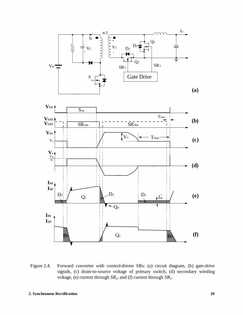
C. Forward Converter with Control-Driven SRs
The forward converter with control-driven SRs and its key waveforms are shown in Fig.
2.4. In this circuit, transistors Q2 and Q3 are driven by gate-drive signals derived from the
primary-switch gate drive. As a result, the conduction times of the synchronous rectifiers are
independent of the transformer-resetting method, but solely depend on the timing of the gate-
drive signals. However, as can be seen from Figs. 2.4(e) and 2.4(f), while driving the SRs from the
control circuit results in the maximum conduction time of Q3, it has no effect on the conduction
time of the magnetizing current though diode D2 during the dead time. Namely, since during the
dead time transistor Q2 is off (gate-drive to Q2 is low), the conduction of diode D2 during the dead
time with control-driven SRs (see Fig. 2.4) is exactly the same as for the self-driven SRs (see Fig.
2.2).
Ideally, the gate-drive timing of SRs should allow no conduction of the body diodes of
the SRs except for the unavoidable conduction of D2 during the dead time. This is only possible
with a very precise gate-drive timing where the gate-drive of one SR is applied or terminated at
the same instant the gate-drive of the other SR is terminated or applied. In practical applications,
this ideally complementary drive is not possible. Accidental, brief overlapping of the gate-drive
signals that turn on both SRs simultaneously would short the secondary, causing an increased
secondary current, and thus would lower efficiency or, in severe cases, would cause converter
failure. To avoid simultaneous conduction of SRs in practical applications, a delay between the
gate-drive signals must be introduced. Since during the delay period no gate-drive signal is
applied to the SRs, the body diodes of the SRs are conducting. This not only increase conduction
2. Synchronous Rectification 20
Vin
+
-VC
S
Vs
+
-
D3Q3
Ion:1
D2
Q2
Ip
Tdead
VsV inn
VGS
VDS
Vin
ID2
IQ2
Q2D2
ID3
IQ3
Q3 D3D3
Son
VC
Qrr
Im-D2
(b)
(c)
(f)
(d)
(e)
(a)
D2
Gate Drive
SR3SR2
VGS2
SR2onVGS3 SR3on
Tdelay
Figure 2.4. Forward converter with control-driven SRs: (a) circuit diagram, (b) gate-drivesignals, (c) drain-to-source voltage of primary switch, (d) secondary windingvoltage, (e) current through SR2, and (f) current through SR3.

2. Synchronous Rectification 21
loss but also introduces reverse-recovery loss. Therefore, the performance of control-driven SRs
is strongly dependent on the timing of the gate drive.
2.1.2. Efficiency Limits of Synchronous Rectification
The efficiency improvement that can be achieved by replacing Schottky rectifiers with
SRs is a complex function of many parameters. The most important are the output voltage,
output current, SR on-resistance, forward-voltage drop of Schottkies that are being replaced by
SRs, the transformer resetting method, efficiency of the converter with Schottkies, and
implementation of SRs (i.e., with or without Schottkies in parallel with SRs). A thorough
estimation of losses in Schottky rectifiers and self-driven SRs and their comparisons for a specific
application are presented in [A7]. In this section, an estimate of overall efficiency improvements
that can be achieved with different SRs implementations is presented.
Generally, the efficiency of a converter can be expressed as
η = + +P
P P Po
o loss REC(2-2)
where Po is the output power, Ploss is the total loss excluding the rectifier loss, and PREC is the
rectifier loss.
For a converter with Schottky rectifiers, the efficiency is

2. Synchronous Rectification 22
ηSHo
o loss SH
PP P P
= + + . (2-3)
Similarly, for the same converter with SRs, the efficiency is
ηSRo
o loss SR
PP P P
= + + . (2-4)
Eliminating Ploss from the above equations, the efficiency of the converter with SRs (ηSR)
can be expressed as a function of the efficiency of the converter with the Schottkies (ηSH)
η ηSRo
o SH SH SR
PP P P
= − +/. (2-5)
The power loss in the Schottky rectifiers can be calculated as
P V ISH SH o= (2-6)
where VSH is the forward-voltage drop of the Schottkies, and Io is the output current.
The power loss of the self-driven SRs, PSRsd , for both RCD-and active-clamp reset is given
by:
P R I D V I D P PSRsd
DS on o dead D o dead gate RREC= − + + +( ) ( )2 1 (2-7)

2. Synchronous Rectification 23
where RDS(on) is the on-resistance of SRs, Ddead = Tdead/Ts is the dead-time duty cycle, VD is the
forward-voltage drop of the antiparallel diodes across SR2 and SR3, Pgate is the gate-driven loss,
and PRREC is the power loss associated with the reverse-recovery of the body diodes of the SRs.
It should be noted that Eq. (2-7) is derived assuming that commutation times Tcomon and
Tcomoff are zero, that synchronous rectifiers SR2 and SR3 have identical on resistance (RDS(on)2 =
RDS(on)3 = RDS(on), and that diodes D2 and D3 have identical voltage drops (VD2 = VD3 = VD) which
are independent of their currents. As a result of the last assumption (VD2 = VD3 = VD), Eq. (2-7)
does not explicitly show dependence on magnetizing current Im− , although it takes into account
the conduction loss this current generates on diode D2.
For self-driven SRs with active-clamp reset, the dead time is very short relative to a
switching period, and therefore, Ddead ≈ 0. However, for the converter with the self-driven SRs
and with the RCD-clamp reset, this duty cycle usually cannot be neglected. In this case, the loss
depends on the duration of the dead time and VD of the antiparallel diodes of the SRs. Generally,
these diodes can be the body diodes of SRs (VD = VBD) or externally added Schottkies in parallel
with SRs (VD= VSH).
The power loss of the control-driven SRs is given by:
P R I D R I I D DSRcd
DS on o dead DS on o m dead delay= − + − −−( ) ( )( ) ( ) ( )2 21
+ + − + +− −V I D V I I D P PD m dead D o m delay gate RREC( ) (2-8)

2. Synchronous Rectification 24
where Ddelay = Tdelay/Ts is the delay-time duty cycle, and Tdelay is the delay time between the SR3
gate-drive turn-off and SR2 gate-drive turn-on as indicated in Fig. 2.4(b).
The gate-drive loss (Pgate) is a function of the gate-to-source voltage of SR, frequency, and
gate charge required to charge SRs’ capacitance to the gate-source voltage [A7]. A method of
estimating this loss for self-driven SRs was presented in [A7]. According to those calculations,
for low frequencies (< 300 kHz), the gate drive loss for today’s SRs is small (< 0.5W), and for
converters with an output power > 50W can be neglected. For control-driven SRs this loss is
higher since it includes also the loss in the external drivers and their associated logic.
The reverse-recovery loss (PRREC) is only presented in implementations where the body
diode of the SR is conduction (no Schottky in parallel with SR). Even when the body diode is
conducting, this loss is relatively small at low frequencies (< 100-150 kHz).
When the gate-drive loss and the reverse-recovery losses are neglected (Pgate = PRREC ≈ 0),
the efficiency of the forward converter with the self-driven SRs for both RCD-and active-clamp
implementations is
1 11 1
η ηSRsd
SH
SH
o
DS on o
SHdead
D
SHdead
VV
R IV
DVV
D= − − − −
( ) ( ) . (2-9)
Since for the forward converter with self-driven SRs and active-clamp reset (Ddead ≈ 0), its
efficiency, ηSRacl , can be expressed in the simplified form as

2. Synchronous Rectification 25
1 11
η ηSRacl
SH
SH
o
DS on o
SH
VV
R IV
= − −
( ). (2-10)
Equations (2-9) and (2-10) can be regarded as the best-case efficiency limits of different
SR implementations. They are more accurate at low frequencies (<100-200 kHz), where the gate-
drive loss and the reverse-recovery loss are small.
The efficiencies of the forward converter with control-driven SRs, ηSRcd , is given by:
1 11 1 1
2
η ηSRcd
SH
SH
o
DS on o
SHdead
DS on o
SH
m
odead delay
VV
R IV
DR I
VII
D D= − − − − −
−
−( ) ( )( ) ( )
− − −
− −VV
II
DVV
II
DD
SH
m
odead
D
SH
m
odelay1 . (2-11)
If magnetizing current Im− « Io so that its loss can be neglected, and if the delay time is
short so that Ddelay ≈ 0, Eq. (2-11) simplifies to Eq. (2-10).
Figure 2.5 shows the plots of Eq. (2-10). These plots present the efficiency of a converter
with SRs (ηSR) as a function of the normalized output voltage (Vo/VSH). The efficiency of the
converter with Schottky rectifiers (ηSH) and α = Io·RDS(on) are the parameters. Parameter α
represents the ratio of the forward-voltage drop of the SR at output current Io to the forward-
voltage drop of the Schottky. Obviously, α needs to be less than 1 to obtain an efficiency
improvement when Schottkies are replaced by SRs.
As can be seen, the efficiency improvement for a given α and a given VSH is lower at
higher output voltages, Vo. Also, for the same output voltage, the efficiency gain achieved by

2. Synchronous Rectification 26
5 10 15 20 25
70
80
90
100
V /V
η
[%
]I R Vo DS on SH( ) / .= 075
SR
o SH
η = 70%SH
η = 90%SH
η = 80%SH
2
(a)
5 10 15 20 25
70
80
90
100
V /V
η
[%
]SR
o SH
η = 70%SH
η = 90%SH
η = 80%SH
I R Vo DS on SH( ) / .= 0 25
2
(b)
Figure 2.5. Efficiency limits of forward converter with self-driven SRs and active-clamp resetand control-driven SRs with small gate-drive timing delay (Ddelay ≈ 0) andmagnetizing current Im
− « Io: (a) α = RDS(on)·Io/VSH = 0.75, and (b) α =0.25.

2. Synchronous Rectification 27
synchronous rectification is higher for converters with higher efficiencies with Schottky diodes
(ηSH), i.e., for converters where the total loss is dominated by the loss in the Schottky rectifiers
(PSH > Ploss ). Similarly, the efficiency improvement is larger for smaller α, i.e., for better SRs
(smaller on-resistance) or lower output currents. For example, from the plot in Fig. 2.5(a) for a
converter with Vo = 3.3 V, Io = 20A, and the efficiency with Schottky rectifiers of ηSH = 0.8,
assuming that VSH = 0.4 V, RDS(on) = 15 mΩ (i.e., α = 0.75 and Vo/VSH = 8.25), the best-case
efficiency improvement is only 2%.
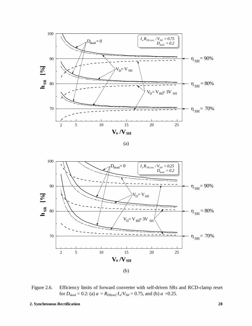
Figure 2.6 shows the plots of Eq. (2-9) for Ddead = 0.2 for the SR implementation with a
Schottky in parallel with SR3 (VD = VSH) and without a Schottky (VD = VBD = 3VSH). Also, for
reference, the curves for Ddead = 0 (see Fig. 2.5) are shown. As can be seen, the efficiency of the
converter with the RCD-clamp reset is strongly dependent on the SR implementation. For the
implementation with Schottky diodes, the efficiency improvement is slightly lower than that of
the control-driven SRs or self-driven SRs with an active-clamp reset. However, when the body
diode of SR3 is used to freewheel the output current, the difference is very significant. In fact,
under certain conditions the efficiency of synchronous rectification can be lower than that of
Schottky diodes, as illustrated in Fig. 2.6(a) for VD = VBD = 3VSH.
2.1.3. Evaluation Results
Evaluations of the discussed SR implementations were performed on 100-kHz, 3.3-V/20-
A forward-converter power stages designed to operate in the 200-400 Vdc input-voltage range.
The power stages for both the RCD-clamp and active-clamp circuits were implemented using the
2. Synchronous Rectification 28
I R VD
o DS on SH
dead
( ) / ..
==0 750 2
5 10 15 20 25
70
80
90
100
V /V
η
[%
]SR
o SH
η = 70%SH
η = 90%SH
η = 80%SH
V = VD SH
V = V = 3VD BD SH
D = 0dead
2
(a)
5 10 15 20 25
70
80
90
100
V /V
η
[%
]
I R VD
o DS on SH
dead
( ) / ..
==0 25
0 2
SR
o SH
η = 70%SH
η = 90%SH
η = 80%SH
V = VD SH
V = V = 3VD BD SH
D = 0dead
2
(b)
Figure 2.6. Efficiency limits of forward converter with self-driven SRs and RCD-clamp resetfor Ddead = 0.2: (a) α = RDS(on)·Io/VSH = 0.75, and (b) α =0.25.

2. Synchronous Rectification 29
IREPE50 MOSFETs (BVDSS = 800 V, ID = 7.8 A, and RDS(on) = 1.2 Ω) for the primary switches and
IR82CQN30 Schottky diodes (VF = 0.3 V @ 20 A and Tj = 125 °C) for the secondary-side
rectifiers. The turns ratio of the transformer for the power stage with the RCD-clamp reset was
Nrcd = 24, while the transformer turns ratio for the active-clamp-reset power stage was Nacl = 28.
In the synchronous rectifier implementations of the experimental power stages, the Schottky
diodes were replaced by the Siliconix synchronous rectifiers SMP60N03-10L (RDS(on) = 10 mΩ, @
Tj = 25 °C, VBD = 0.9 V @ 20 A and Tj = 25°C, Ciss = 2600 pF @ VDS = 25 V, and Coss = 1500 pF
@ VDS = 25 V).
Figure 2.7(a) shows the measured efficiency of the experimental converter with the RCD-
clamp reset and self-driven SRs at full output current (Io = 20 A) as a function of the input
voltage. Also shown in Fig. 2.7(a) is the efficiency of the converter with Schottky rectifiers. As
can be seen, the efficiency of the SR implementation without Schottky diodes connected in
parallel with the SRs is lower than that of the converter with the Schottky rectifiers. As has been
explained earlier, the efficiency loss is caused by the excessive power loss in the body diode of
SR3 during the dead time. If Schottky diodes in parallel with SRs are added, the efficiency of
synchronous rectification is improved. It is 0.7-1.2% higher than that of the Schottky rectifiers.
The calculated efficiencies of the converter with the SRs obtained from Eq. (2-9), are also
shown in Fig. 2.7(a). As can be seen, they are in good agreement with the measured efficiencies
for both the SR implementation with and without the Schottky diodes in parallel with the SRs.
For the SR implementation without the Schottky diodes in parallel with the SRs, the maximum
discrepancy between the calculated and measured efficiencies is 0.6%. It should be noted that the
measured efficiencies in the entire input-voltage range are lower than the calculated efficiencies.

2. Synchronous Rectification 30
200 250 300 350 40077
78
79
80
81
82
83
84
85
V /V
Pow
er S
tage
Eff
icie
ncy
[%]
o SH
MeasuredCalculated
Vo = 3.3 VIo = 20 A
self-driven synchronous rectifiers (SMP60N03-10L)w/o Schottkies in parallel
self-driven synchronous rectifiers (SMP60N03-10L)w Schottkies (82CNQ30) in parallel
Schottkies rectifier (82CNQ30)
(a)
200 250 300 350 40082.5
83
83.5
84
84.5
85
85.5
86
V /V
Pow
er S
tage
Eff
icie
ncy
[%]
o SH
MeasuredCalculated
Vo = 3.3 VIo = 20 A
self-driven synchronous rectifiers (SMP60N03-10L)w/o Schottkies in parallel
Schottkies rectifier (82CNQ30)
D = 0delay
D = 0.01delay
(b)
Figure 2.7. Measured efficiencies of forward-converter power stage with self-driven SRs: (a)with RCD-clamp reset, and (b) with active-clamp reset.
2. Synchronous Rectification 31
The primary reason for these discrepancies is the reverse-recovery loss of the SRs’ body diodes
which was neglects when deriving Eq. (2-9). An indirect proof for this claim is the fact that the
discrepancies between calculated and measured efficiencies of the implementation with the
Schottky diodes in parallel with the SRs are less than 0.2% in the entire input-voltage range. The
improved agreement between the calculated and measured efficiencies in this case is the result of
the suppressed conduction of the body diodes of the SRs, and consequently, of the elimination
of their reverse-recovery losses.
It should be noted that the calculated efficiencies presented in Fig. 2.7(a), as well as in the
following figures, were obtained by taking into account the temperature effects on the on-
resistance of the synchronous rectifier and Schottky diode forward-voltage drop. Namely, during
the efficiency measurements, the case temperatures of the SRs and Schottky diodes were also
recorded along with the other relevant data (e.g., reset-voltage dead time duration). Based on the
estimated losses and thermal resistance of the component packages, the junction temperatures of
the SRs and Schottkies were determined, and their parameters were taken from the data sheets at
the calculated junction temperatures. In addition, exactly the same set-up is used to measure the
efficiencies of all experimental circuits, ensuring a high accuracy of the relative (comparison)
measurements.
Figure 2.7(b) shows the measured efficiency of the experimental forward converter with
the active-clamp reset and the self-driven SRs. As can be seen by comparing Figs. 2.7(a) and
2.7(b), the efficiency of this converter with the Schottky rectifiers is approximately 1% (83.5%
versus 82.5%) higher compared to the corresponding converter with the RCD-clamp reset. This is
primarily due to a reduced power loss on the primary side of the converter because of a higher

2. Synchronous Rectification 32
maximum duty cycle, and consequently, higher turns ratio of the transformer. The achieved
efficiency improvement by synchronous rectification is approximately 1.5-2% depending on the
input voltage.
The calculated efficiencies using Eqs. (2-9) and (2-10) are also shown in Fig. 2.7(b). As
can be seen, the agreement between the calculated and measured efficiencies is good. As
expected, better agreement was obtained by using a more accurate expression given by Eq. (2-9).
In fact, the maximum discrepancy between the theoretical and experimental efficiencies for Eq.
Eq. (2-9) is 0.7%. As in the case of the self-driven SRs with the RCD-clamp reset, this
discrepancy can be attributed primarily to the reverse-recovery losses of the SRs which are not
taken into account in Eqs. (2-9) and (2-10).
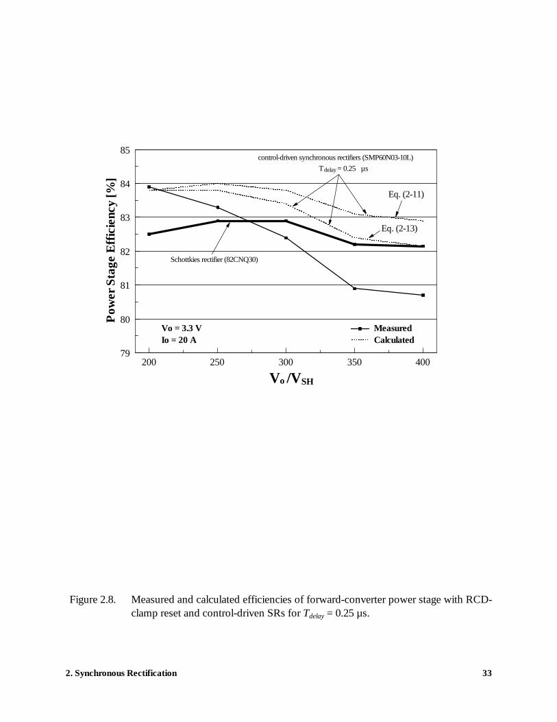
Figure 2.8 shows the measured efficiency of the experimental forward converter with the
RCD-clamp and control-driven SRs for Tdelay = 0.25 µs. From Fig. 2.8, at the input voltages below
250 V, the efficiency of the converter with SRs is slightly better than that of the converter with
Schottkies. Specifically, the maximum efficiency improvement that occurs at low line (200 V) is
1.4%. However, for the input voltages higher than 250 V, the efficiency of the SR implementation
is lower than the efficiency of the Schottky-diode implementation. The efficiency difference
above 250 V increases as the input voltage increases, and reaches the maximum at high line (400
V), where the efficiency of the converter with SRs is 1.6% lower than the efficiency of the
Schottky counterpart.
The calculated efficiency curve of the converter with SRs obtained from Eq. (2-11) is also
shown in Fig. 2.8. Since the measured clamp voltage is VC ≈ 300 V, the measured magnetizing
inductance of the transformer is Lm ≈ 7.8 mH, and the estimated equivalent capacitance at the
2. Synchronous Rectification 33
200 250 300 350 40079
80
81
82
83
84
85
V /V
Pow
er S
tage
Eff
icie
ncy
[%]
o SH
MeasuredCalculated
Vo = 3.3 VIo = 20 A
control-driven synchronous rectifiers (SMP60N03-10L)T = 0.25 µs
Schottkies rectifier (82CNQ30)
delay
Eq. (2-13)
Eq. (2-11)
Figure 2.8. Measured and calculated efficiencies of forward-converter power stage with RCD-clamp reset and control-driven SRs for Tdelay = 0.25 µs.

2. Synchronous Rectification 34
drain of the primary-switch MOSFET (including the voltage dependence of MOSFETs Coss) is CS
≈ 300 pF, the value of magnetizing current Im− used in the efficiency calculations, according to
Eq. (2-1), is
I Am−
− −=
⋅ ⋅≈24
300
7 8 10 300 1015
3 12. /. . (2-12)
As can be seen from Fig. 2.8, the calculated efficiency curve is far off from the measured
curve. In fact, the calculations predict the efficiency improvements over the entire input-voltage
range when Schottkies are replaced by the SRs. The maximum discrepancy between the
calculated and measured data occurs at high lime (400 V), and it is 2.2%. The major reason for
this discrepancy was found to be related to the power losses due to the parasitic oscillations on
the secondary side during the dead time. These oscillations are generated by the parasitic
resonance between the parasitic inductance (leakage, interconnect, and package) of the loop
consisting of the secondary winding of the transformer, SR2, and SR3, and the secondary-side
parasitic capacitance (parasitic capacitance of the winding and switches). To illustrate the
problem, Fig. 2.9 shows the voltage waveforms of the primary switch and synchronous rectifiers
SR2 and SR3 at Vin = 300 V. As can be seen from Fig. 2.9, the drain-to-source voltage of the
primary switch shows oscillations during the dead time. Although not observable in Fig. 2.9,
these oscillations are also present in the SR2 and SR3 voltage waveforms as seen in Fig. 2.10,
which shows the blown-up SR2 and SR3 waveforms during the dead time. Since during the dead
time, transistor Q3 of SR3 and diode D2 of SR2 are conducting, the secondary current during the
dead time can be estimated by dividing the voltages across SR3 by its on-resistance. As indicated

2. Synchronous Rectification 35
Figure 2.9. Oscillogram of key voltage waveforms of forward converter with RCD-clamp andcontrol-driven SRs. From top to bottom: drain-to-source voltage of primaryswitch VDS, SR3 voltage VSR3, and SR2 voltage VSR2. Scale: VDS = 200 V/div.,; VSR3 =10 V/div.; VSR2 = 6.6 V/div. Time = 1.3 µs.
DEAD
VDS
VSR3
Q3 - on
D2 - on
reverse-recovery
induced spike
reverse-recovery
induced spike
VSR2
0
0
0

2. Synchronous Rectification 36
Figure 2.10. Blown-up voltage waveforms from Fig. 2.9 during dead time. From top to bottom:SR3 voltage VSR3, and SR2 voltage VSR2. Scale: VSR3 = 200 mV/div.; VSR2 = 200mV/div. Time = 0.7 µs.
VSR3
Q - on
VSR3
Q3 - on
DEAD
TIME
Ipk

2. Synchronous Rectification 37
in Fig. 2.10, the peak of the SR3 current during the dead time is IpkSR3 ≈ 25 A, while the peak-to-
peak resonant (ringing) current amplitude (oscillatory component of the SR3 current) is IrSR3 ≈
12A. This relatively large parasitic, ringing current that circulates in the loop consisting of the
secondary winding, D2, and Q3 causes an additional power loss which is not taken into account in
Eq. (2-11). The amount of this additional power loss depends mainly on the on-resistance of SR3,
secondary winding resistance (at the ringing frequency) and the rms value of the ringing current.
It should be noted that the power loss of the ringing current on diode D2 of SR2 is relatively small
because the dynamic resistance of diode D2 is much smaller than the on-resistance of transistor
Q3. That is the reason that, although the parasitic oscillations are also present in the converter with
self-driven SRs (see Fig. 2.3), they do not significantly affect the efficiency. Namely, in the self-
driven implementation, both diodes D2 and D3 are conduction during the dead time.
The effect of the above described circulating ringing current is to decrease the efficiency
of the converter. Its effect is more pronounced at higher line voltages where the dead-time
duration is longer. As a result, the efficiency of the converter with control-driven SRs shows a
relatively steep fall-off as the input voltage increases compared with the converter with serf-
driven SRs.
Figure 2.8 also shows the calculated efficiency curve that takes into account the effect of
secondary-side circulating ringing current during the dad time. The modified expression that is
used to calculated this curve is

2. Synchronous Rectification 38
[ ]1 11 1
22 2
η ηSRcd
SH
SH
o
DS on o
SHdead
loop o m r
SHdead delay
VV
R IV
DR I I I
VD D= − − − −
− +−
−( ) ( )
( ) /( )
− − −
− −VV
II
DVV
II
DD
SH
m
odead
D
SH
m
odelay1 (2-13)
where Rloop is the total resistance of the secondary-side loop consisting of the secondary winding,
SR2, and SR3. Practically, this resistance is the sum of the secondary winding resistance at the
ringing frequency and the on-resistance of SR3.
As can be seen from Fig. 2.8, although Eq. (2-13) gives better agreement between the
calculated and measured curves (maximum difference reduced to 1.6%), a significant discrepancy
between these two curves is still present. While 0.6%-0.7% of this discrepancy can be attributed
to the reverse-recovery loss, as in the case of the self-driven converters, the remaining difference
can only be explained by the inaccuracy in determining the magnitude of the ringing current.
Namely, it is not possible to measure this current directly because any current-measuring device
(including a transformer probe) was found to significantly disturb the operation of the circuit by
introducing a relatively significant inductance in the sedentary side loop. As a result, the ringing
current must be measured indirectly (e.g., measuring the voltage waveform across SR3 using a
scope), and then estimated from the measurement, which inadvertently introduces an error.
Finally, Fig. 2.11 show the measured efficiency of the experimental forward converter
with RCD-clamp reset and control-driven SRs for different delay times between the SRs gate-
drive signals. As can be seen, the efficiency is very sensitive to the duration of the delay time. It

2. Synchronous Rectification 39
200 250 300 350 40077
78
79
80
81
82
83
84
85
V /V
Pow
er S
tage
Eff
icie
ncy
[%]
o SH
Vo = 3.3 VIo = 20 A
Schottkies rectifier (82CNQ30)T = 0.25 µsdelay
T = 0.25 µsdelay
T = 0.25 µsdelay
T = 0.5 µsdelay
control-driven synchronous rectifier (SMP60N03-10L)
Figure 2.11. Measured efficiencies of forward converter power stage with RCD-clamp resetand control-driven SRs with different delay times.

2. Synchronous Rectification 40
decreases as the delay time, Tdelay, increases. In fact, for longer delay time, the efficiency
improvement at lower input voltage also decreases.
2.1.4. Summary
Different implementations of synchronous rectification in the forward-converter topology
are discussed, and the effect of the transformer resetting mechanism on the performance of the
self-driven synchronous-rectifiers (SRs) is analyzed. An estimate of the upper limit of the
efficiency improvement of synchronous rectification relative to the Schottky diode
implementation is derived, as shown in Figs. 2.5 and 2.6. The limit is a function of the output
voltage, output current, on-resistance of SRs, forward-voltage drop of Schottkies that are being
replaces with SRs, efficiency of the converter with Schottkies, and SR implementation. These
figures can be used for general applications to determine the efficiency improvement of
employing synchronous rectifiers in forward converters to replace conventional diode rectifiers
once the diode efficiency is provided or estimated. The discussed SR implementations are
evaluated experimentally on a 3.3-V/20-A, off-line power state. The achieved efficiency
improvements for this application were, as predicted, relatively modest (1-2%).

2. Synchronous Rectification 41
2.2. Synchronous Rectification in Flyback Converter
A number of applications of the SR in the flyback converter have also been reported
[A23-A25]. However, in all of these applications, the main purpose of the SR was to provide the
post-regulation of the output voltage and not to maximize the conversion efficiency. Specifically,
in [A23-A25], the SR is used as a voltage-controlled resistor in a control loop which adjusts the
SRs resistance so that the output voltage is maintained within the regulation range, as shown in
Fig. 2.12. Generally, the regulation range of these post-regulation approaches is limited to the
forward-voltage drop of the SR body diode, i.e., ~ 0.7 V. Moreover, since the voltage drop across
the SR is not minimized because of the resistance modulation, the conversion efficiency of these
post regulators is reduced, compared to that of the converter with the “true” SR.
This section evaluates the theoretical and practical limits of the efficiency improvements
for various implementations of the flyback converter with the SR with respect to the
corresponding converter with the diode rectifier. Specifically, the design considerations and
performance evaluations of the constant-frequency (CF) continuos-conduction-mode (CCM), CF
discontinuous-conduction-mode (DCM), variable-frequency (VF) DCM, and zero-voltage-
switched (ZVS) DCM flyback converters with SR are discussed. The experimental verification
was implemented for an off-line, universal-input, 15-V/36-W flyback adapter application.

2. Synchronous Rectification 42
DTRi
v
Vo1 = < v >
+
-Vo1
+
-
Vin
+ -vi
+
-Vo2
D
TR
Figure 2.12. Synchronous rectifier in flyback converter used as post regulator in multiple-output applications.

2. Synchronous Rectification 43
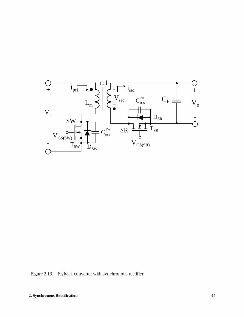
2.2.1. Synchronous Rectifier Implementations
A flyback converter with the SR is shown in Fig. 2.13. For proper operation of the
converter, conduction periods of primary switch SW and secondary-side switch SR must not
overlap. To avoid the simultaneous conduction of the SW and the SR, a delay between the turn-
off instant of switch SW and the turn-on instant of the SR as well as between the turn-on instant
of the SW and turn-off instant of the SR must be introduced in the gate-drive waveforms of the
switches. With properly designed gate drives, the operation of the circuit shown in Fig. 2.13 is
identical to that with a conventional diode rectifier. Namely, during the time switch SW is turned
on, energy is stored in the transformer magnetizing inductance and transferred to the output after
SW is turned off.
Generally, the circuit sown in Fig. 2.13 can work in CCM or DCM either with a constant
or variable switching frequency PWM control. Design considerations and SR loss estimates for
various modes of operation and different control approaches are given next.
2. Synchronous Rectification 44
isec +
-
Vo
+
-
Vin
SWSR
ipri
CossSR
DSR
TSRCossSW
DSWTSW
LmCF
Vsec+
-
VGS(SW)VGS(SR)
n:1
Figure 2.13. Flyback converter with synchronous rectifier.

2. Synchronous Rectification 45
A. Constant-Frequency (CF) Continuous-Conduction-Mode (CCM)
The key waveforms of the flyback converter with the SR operating in CCM are given in
Fig. 2.14. As can be seen from Fig. 2.14, during delay times TDon and TD
off , secondary current isec
flows through the body diode of the SR. The conduction of body diode DSR not only increases
the conduction loss, but also introduces a reverse-recovery loss when primary switch SW is
turned on. The conduction loss of the SR is given by the sum of the channel-resistance loss and
body-diode loss as
P RI
DI D
V I T T fcondSR
DS ono sec
D D Don
Doff
s= − + −
+ +( )( )
( )2 2
11
12∆
(2-14)
where RDS(on) is the SR on-resistance, D = Ton/Ts is the duty-ratio of the primary switch SW, Io is
the output current, ∆Isec is the secondary peak-to-peak ripple current, VD and ID are the forward-
voltage drop and current of the body diode, respectively.
The reverse-recovery loss of the SR body diode is given by
P Q VVn
fRRSR
RR oin
s= +( ) (2-15)
where QRR is the recovered charge of the SR body diode, and Vo + Vin/n is the steady-state reverse
voltage across the SR.

2. Synchronous Rectification 46
isec
TDon
TDoff
Vsec
SW SRVGS
ipri
QRR
-VoToffTon
DSRVDS(SW)
Vin
Vin+nVo
Vinn
∆isecTSR Io
reverse-recoverycharge
Ts
Figure 2.14. Key waveforms of CF CCM flyback converter with SR. Body diode of SRconducts in shaded area ( ).

2. Synchronous Rectification 47
In addition to PcondSR and PRR
SR losses, the CF CCM converter in Fig. 2.13 exhibits a loss
each time the SR is turned off (i.e., each time the SW is turned on) because of a parasitic
resonance between CossSR and the leakage inductance of the transformer (see Fig. 2.21). Since the
parasitic resonance must be damped by a snubber to limit the maximum voltage across the SR,
the resonance dies out completely before SR is turned on again. As a result, the power loss due to
this parasitic resonance can be calculated from
P C VVn
foffSR
ossSR
oin
s= +12
2( ) . (2-16)
Finally, for proper operation of the circuit, the SR must be turned off before primary
switch SW is turned on (delay time TDoff in Fig. 2.14). Therefore, the flyback converter with the
SR cannot be self-driven from the secondary winding of the transformer. In fact, the circuit
shown in Fig. 2.13 requires an external control circuit to turn off the SR.
B. CF Discontinuous-Conduction-Mode (DCM)
The key waveforms of the constant-frequency flyback converter with the SR operating in
DCM are shown in Fig. 2.15. In DCM, the energy stored in the magnetizing inductance of the
transformer during the on time of switch SW is completely discharged during the subsequent off
time. As can be seen from Fig. 2.15, secondary current isec reaches zero before primary switch SW
is turned on. To prevent the discharging of the output filter capacitor through a conducting SR,
the SR channel conduction (transistor TSR) must be terminated at the moment isec reaches zero, or

2. Synchronous Rectification 48
isec
SW SR
VDS(SW)
VGS
ipri
VinVin-nVo
TDCM
Vin+nVo
t0 t2t1 t3 t4
Von
DSR
IoTSR
Figure 2.15. Key waveforms of CF DCM flyback converter with SR. Body diode of SRconducts in shaded area ( ).

2. Synchronous Rectification 49
a short while after. Therefore, the DCM flyback converter with the SR requires a zero-current-
crossing detector in the control circuit.
After the SR is turned off, the magnetizing inductance of the transformer Lm and
capacitance Ceq = C C nossSW
ossSR+ / 2 starts resonating, as shown in Fig. 2.15. For a converter with
a regulated output, the duration of resonant interval TDCM in Fig. 2.15 changes significantly with
the input voltage and less dramatically with the output current. As a result, the voltage across the
primary switch at the moment of its turn on can range anywhere between Vin + nVo and Vin - nVo,
producing the capacitive turn-on loss of
P C V fcap SW ossSW
on s( ) = 12
2 (2-17)
where Vin - nVo ≤ Von ≤ Vin + nVo. Since Pcap(SW) is maximum at the peaks of the VDS(SW) oscillation
and minimum at its valleys, the efficiency of the converter has strong fluctuations with the input
voltage. In addition, because typical SRs have a much larger output capacitance CossSR than the
Schottky rectifiers, the characteristic impedance, Z L Cm m eq= / , of the resonant tank
consisting of Lm and Ceq, is much lower for the converter with an SR compared to that with a
Schottky diode. As a result, the resonant-tank current of the converter with an SR is much higher
than that of the converter with a Schottky, causing a larger conduction loss. For certain line and
load conditions, this power loss can completely offset the conduction power-loss savings
obtained by the SR, making the efficiency of the converter with the SR lower than that of the
converter with the diode rectifier.

2. Synchronous Rectification 50
Finally, it should be noted that in the DCM flyback converter reverse-rectifier loss PRRSR is
eliminated because the rectifier current becomes zero before primary switch SW is turned on.
C. Variable-Frequency (VF) DCM
Capacitive switching loss Pcap(SW) can be minimized, and parasitic oscillation caused by the
interaction between Lm and Ceq can be eliminated if the primary switch SW is turned on at the
moment VDS(SW) reaches its minimum voltage, Vin - nVo, the first time after the SR is turned off, as
shown in Fig. 2.16. This can be accomplished by sensing the zero-current-crossing of isec and
turning on SW after a constant delay Tdealy which is equal to one half of the parasitic-resonance
period, i.e.,
T L Cdelay m eq= π . (2-18)
With this variable-frequency control, the efficiency fluctuations with the input voltage are
eliminated. It should be noted that with the VF control, the switching frequency is minimum at
low line and full load, and it increases as the line increases and/or load decreases.
The conversion efficiency at low line of the variable-frequency DCM converter can be
always made higher than the efficiency of the corresponding constant-frequency counterpart. In
addition, the high-line efficiency of the VF DCM converter can also be higher than that of the CF
DCM implementation if the power-loss savings due to the elimination of the parasitic oscillations
and the minimization of the turn-on voltage Von are higher than the increased switching losses and
magnetic losses due to the increased switching frequency.

2. Synchronous Rectification 51
Vin
isec
SW SR
VDS(SW)
VGS
ipri
Vin-nVo
TdelayVin+nVo
t0 t2t1 t3 t4
DSR
IoTSR
Figure 2.16. Key waveforms of VF DCM flyback converter with SR. Body diode of SRconducts in shaded area ( ).

2. Synchronous Rectification 52
D. VF Zero-Voltage-Switched (ZVS) DCM
As can be seen from Fig. 2.16, if the amplitude of the oscillation after the turn-off of the
SR is larger than the input voltage, i.e., if
Vin < nVo, (2-19)
primary-switch voltage VDS(SW) will fall to zero before the switch is turned on at the moment t4 = t3
+ Tdelay [A26, A27]. Therefore, for Vin < nVo, the VF flyback converter can achieve ZVS, i.e., the
capacitive turn-on loss of the primary switch can be eliminated. While the ZVS condition in Eq.
(2-19) may be met for certain designs at low input-voltages, generally it is not met at higher input
voltages. As a result, at higher input voltages, the VF flyback converter with gate-drive timing
given in Fig. 2.16 operates with partial ZVS.
However, the complete ZVS of the primary switch in the VF flyback converter with the
SR can be achieved in the entire input-voltage range if the turn-off instant of the SR after the
secondary current zero-crossing is delayed enough to allow a negative secondary current to build
up, as shown in Fig. 2.17. To achieve ZVS in the entire input-voltage range, the energy stored in
magnetizing inductance Lm by the negative secondary current IZVS must be large enough to
discharge primary switch capacitance CossSW from voltage Vin + nVo down to zero, i.e.,
In V nV
ZZVSin o
m≥
−(max) ( )2 2
. (2-20)

2. Synchronous Rectification 53
Vin
isec
SW SR
VDS(SW)
VGS
ipri
Vin-nVo
Vin+nVo
t0 t2t1 t3 t4
TdelayZVS
IZVS
TSR Io
DSR
Figure 2.17. Key waveforms of VF ZVS DCM flyback converter with SR. Body diode of SRconducts in shaded area ( ).

2. Synchronous Rectification 54
Therefore, to build up the necessary IZVS, the turn-off of the SR should be delayed after the zero-
crossing of isec for
TL I
n VdelayZVS m ZVS
o= ⋅
⋅2 , (2-21)
as shown in Fig. 2.17.
Finally, it should be noted that in VF ZVS DCM flyback converter with the SR the
capacitive turn-on switching loss of the primary switch is traded off for the conduction loss.
Namely, according to Fig. 2.17, due to the negative secondary current, the RMS value of the
secondary current is slightly increased. Therefore, the VF ZVS converter in Fig. 2.17 might not
necessarily achieve higher efficiency compared to the VF converter with partial ZVS (Fig. 2.16).
2.2.2. Efficiency Limit of Synchronous Rectification
Generally, in a flyback converter, the substitution of the diode rectifier with an SR affects
the conduction and switching losses of the rectifier. In addition, the employment of an SR allows
for the implementation of VF flyback converter with complete ZVS, i.e., without any primary-
switch capacitive turn-on switching loss Pcap(SW). Table 2-I summarizes theoretical rectifier
conduction loss Pcond, rectifier switching losses, Psw = Poff + PRR, and the primary switching loss,
Pcap(SW), of the flyback converter with diode rectifier (DR) and the SR.
The efficiency of a converter with the diode rectifier can be expressed as

2. Synchronous Rectification 55
TA
BL
E 2
-I.
PO
WE
R L
OSS
CO
MP
AR
ISO
NS
OF
FL
YB
AC
K C
ON
VE
RTE
RS
WIT
H D
IOD
E R
EC
TIF
IER
(D
R) A
ND
SY
NC
HR
ON
OU
S R
EC
TIF
IER
(S
R).
CF
CC
MC
F D
CM
VF
DC
MV
F Z
VS
DC
M
DR
VI
Fo
VI
Fo
VI
Fo
not p
ossi
ble
to im
plem
ent
SRR
ID
ID
DS
ono
sec
()
()
22
11 12
−+
−
∆
++
VI
TT
fD
DDon
Doff
s(
)
RI
DD
Son
o(
)(
)4
31
2 −R
ID
DS
ono
()
()
43
1
2 −
RI
DD
Son
o(
)(
)4
31
2 −
++
−I
II
DZV
So
ZVS
21
3(
)
DR
*C
VV n
QV
V nf
To
inRRD
Ro
ins
22
()
()
++
+
0
0no
t pos
sibl
e to
impl
emen
t
SRC
VV n
QV
V nf
oss
SR
oin
RRSRo
ins
22
()
()
++
+
0
00
DR
CV
nVf
oss
SW
ino
s2
2(
)+
CV
fos
sSW
ons
22
CV
nVf
oss
SW
ino
s2
2(
)−
not p
ossi
ble
to im
plem
ent
SRC
VnV
fos
sSW
ino
s2
2(
)+
CV
fos
sSW
ons
22
CV
nVf
oss
SW
ino
s2
2(
)−
0
* N
ote
that
for S
chot
tky
rect
ifier
s, Q
RR ≈
0.
P con
d
P sw =
P off +
P RR
P cap
(SW
)

2. Synchronous Rectification 56
ηDRo
o condDR
swDR
cap SWDR
other
P
P P P P P=
+ + + +( )(2-22)
where Po is the output power and Pother is the loss other than the conduction and switching losses
of the rectifier, and the capacitive turn-on switching loss of the primary switch.
Similarly, the efficiency of the flyback converter with the SR can be written as
ηSRo
o condSR
swSR
cap SWSR
other
PP P P P P
=+ + + +( )
. (2-23)
By eliminating Pother from Eqs. (2-22) and (2-23), the efficiency difference between the SR and
the diode rectifier implementations can be calculated as
∆η ∆∆= − = −η η η
ηSR DRREC DR
o REC DR
PP P
2
(2-24)
where
∆P P P P P P PREC condDR
condSR
swDR
swSR
cap SWDR
cap SWSR= − + − + −( ) ( ) ( )( ) ( ) . (2-25)
Using the power loss expressions from Table 2-I and knowing the device characteristics
and the circuit parameters, the efficiency improvement of the flyback converter with the SR can
be calculated. As an example, Fig. 2.18 presents the calculated efficiencies for the discussed four
implementations of the converter with the SR as functions of the load current. In Fig. 2.18, it is

2. Synchronous Rectification 57
assumed that the diode rectifier versions of the converter have conversion efficiencies of 89%,
which correspond to the efficiencies of the experimental circuit discussed in the next section.
As can be seen from Fig. 2.18, the efficiency of the ZVS DCM implementation (solid line)
is highest at low power levels (i.e., for Io ≤ 5-6 A) because the switching turn-on loss of the
primary switch contributes significantly to the total loss in the other implementations. For the
same range of the output power, the CF CCM implementation exhibits the lowest efficiency due
to the dominant effect of the turn-on switching loss of the primary switch and the turn-off
switching loss of the SR. For example, at Io = 2.4 A (which corresponds to the full-load current of
the experimental converter presented in the next section), the efficiency of the ZVS DCM
implementation with the SR is approximately 3% higher than the efficiency of the corresponding
circuit with the Schottky rectifier. However, at Io = 2.4 A, the efficiency of the CCM
implementation with the SR at Io = 2.4 A is 1% lower than the efficiency of the same circuit with
the Schottky rectifier.
At higher power levels, the conduction losses of the primary switch and the SR start
dominating the total loss. As a result, the CF CCM implementation exhibits the highest efficiency
at Io > 15 A due to its smallest primary and secondary RMS currents. On the other hand, the
efficiency of the CF DCM implementation monolithically decreases as the load current (output
power) increases. In fact, as can be seen from Fig. 2.18, for Io > 10 A the efficiency of the CF
DCM implementation is lower than that of the Schottky implementation. Also, as the load
current, and therefore the conduction losses, become larger, the efficiencies of the VF DCM and
ZVS DCM implementations converge because the power savings brought about by soft-
switching in ZVS DCM implementation are less significant.

2. Synchronous Rectification 58
86
87
88
89
90
91
92
93
94
0 5 10 15 20Io [A]
η [%
]
VF DCM
CF CCM
ZVS DCM
CF DCM
2.4
Diode Rectifier
V in = 200V, Vo=15V,n = 6.3, fs = 100kHz,
RDS(on) = 10mΩ, VF = 0.7V
Figure 2.18. Theoretical efficiency estimates.
2. Synchronous Rectification 59
Finally, as the output current continues to increase, so that the voltage drop across the SR,
RDS(on)·iRMS, approaches that of the Schottky rectifier VF, the efficiencies of the CF CCM, VF
DCM, and ZVS DCM implementations approach that of the Schottky-rectifier implementation.
As can be seen from Fig. 2.18, at Io = 20 A the efficiencies of the VF DCM and ZVS DCM
implementations fall to the level of the Schottky implementation efficiency. The CF CCM
implementation efficiency drops to that of the Schottky-rectifier implementation at Io > 20 A due
to lower isecRMS . The only way to achieve efficiency improvements at higher load currents i.e.,
when RDS(on) ·iRMS ≈ VF, is to resort to paralleling of SRs in order to reduce the effective RDS(on).
2.2.3. Evaluation Results
The discussed SR implementations were experimentally evaluated on a 15-V/2.4-A
flyback converter designed to operate in the 100-370 Vdc input-voltage range. The diode-version
power stages were implemented with Motorola MTP6N60 (VRRM = 600 V, RDS(on) = 1.2 Ω @ Tj =
25°C, Coss = 350 pF @ VDS = 25 V) MOSFETs for the primary switches and two IR 10CQT150
(VRRM = 150 V, VF = 0.73 V @ 5 APK, Tj = 125 °C, CT = 200 pF @ VR = 25 V) Schottky diodes in
parallel for the secondary rectifiers. In implementations of the power stages with SRs, the
Schottky diodes were replaced with IXYS IXFK100N10 (VRRM = 100 V, RDS(on) = 11 mΩ @ Tj =
25 °C, Coss = 3300 pF @ VDS = 25 V, VBD = 1.1 V) MOSFETs. The turns-ratio of the transformer
for the CCM implementation was n = 64:10 (Lm = 637 µH), and the converter was operated in
CCM at full-load over the entire input line range with switching frequency fs = 100 kHz [E8]. The
2. Synchronous Rectification 60
transformer used for all other implementations (CF DCM, VF DCM, and ZVS DCM) had a turns
ratio of n = 38:6 (Lm = 229 µH).
Figure 2.19 shows the control and drive circuit for the variable frequency DCM flyback
converter implementations with the SR. As can be seen from Fig. 2.19, the converter has a
detector which senses zero crossings of secondary current isec. The delay time between the zero
crossing of secondary current isec and the turn-off of the SR is set by the R-C time constant of the
TdelayZVS circuit which is connected to the output of the zero-crossing detector comparator.
Resistors R3 and R4 are used to set the hysteresis of the zero-crossing detector. The VF control of
the converter is achieved by employing the UC 3852 IC controller. Also, an R-C delay circuit is
used on the primary side to set a proper delay between the turn-off of the SR and the turn-on of
the primary switch.
A. CF CCM
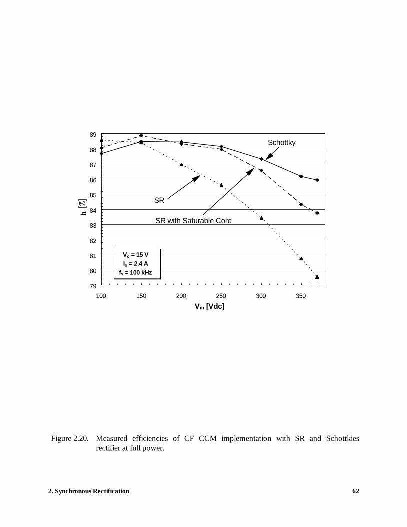
Figure 2.20 shows the measured efficiencies of the CF CCM experimental converters with
the Schottky diode and the SR. Because the SR body diode conducts current during delay times,
TDon and TD
off in Fig. 2.20, the rectifier turn-off loss becomes significant at high frequencies. In
fact, in the experimental 100 kHz converter, the excessive rectifier turn-off loss in the SR
converter exceeds the conduction loss savings. As predicted in Section III, the efficiency of the
SR implementation is lower than that of the Schottky implementation, especially at high line,
where the reverse-recovery loss given by Eq. (2-15) is highest.

2. Synchronous Rectification 61
PWM ControllerUC3852N
Driver TC4429
VGS(SR)Vo feedbackcontrol CKT
ipri
Driver TC4420
isec
LM393
VGS(SW)
+
-
Rpri RsecR2R1
Tdelay TdelayZVS
R4R3
Rdetzero-
crossingdetector
SW
Figure 2.19. Control and drive circuit for VF DCM flyback converter with SR. The thick linesbelong to power stage.
2. Synchronous Rectification 62
79
80
81
82
83
84
85
86
87
88
89
100 150 200 250 300 350
Vin [Vdc]
η
Schottky
SR
SR with Saturable Core
Vo = 15 VIo = 2.4 A
fs = 100 kHz
Figure 2.20. Measured efficiencies of CF CCM implementation with SR and Schottkiesrectifier at full power.

2. Synchronous Rectification 63
(a)
(b)
Figure 2.21. SR turn-off waveforms of CF CCM converter with SR: (a) w/o saturable core; (b)w/ saturable core.
VDS(SR)
I(SR)
VDS(SW)
VDS(SR)
I(SR)
VDS(SW)

2. Synchronous Rectification 64
Figure 2.21(a) shows the SR turn-off waveforms which are initiated by the primary switch
SW turn-on. The fast-rising voltage VDS(SR) causes large superimposed capacitor charging and
body reverse-recovery currents. To suppress these currents, a saturable core was connected in
series with the SR to slow down the rate of VDS(SR) rise, as shown in Fig. 2.21(b). As can be seen
from Fig. 2.21(b), with the saturable-core snubber, not only the reverse current amplitude was
reduced significantly, but also the rectifier voltage stress was decreased. As a result, the
conversion efficiency was improved, as can be seen in Fig. 2.20. However, this approach cannot
completely eliminate the body diode reverse-recovery problem. In fact, output capacitance of the
SR, CossSR , is significantly higher than the junction capacitance of the two paralleled Schottky
diodes CT (CossSR = 3300 pF vs. 2CT = 800 pF), causing a higher capacitor charging loss according
to Eq. (2-16). Therefore, at 36-W power level the CCM converter with the Schottky rectifier
exhibits higher efficiency than that with the SR.
B. CF DCM
Figure 2.22 shows an oscillogram with the key waveform of the CF DCM converter with
the SR. During the resonant-interval TDCM, Lm-Ceq resonance can be clearly seen in both I(SR) and
VDS(SW) waveforms. The measurement points of the efficiency plot shown in Fig. 2.23 were
collected at the valleys, Vin - nVo, and the peaks, Vin + nVo, of VDS(SW). As can be seen from Fig.
2.23, the resonant peak points correspond to the lowest efficiencies, and the resonant valley
points correspond to the highest efficiencies. The SR and diode rectifier implementations have
peaks and valleys at different time instants within a switching period because the resonant period
in the SR converter is longer due to a higher Coss value. Therefore, at certain input voltages, the
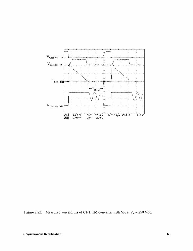
2. Synchronous Rectification 65
Figure 2.22. Measured waveforms of CF DCM converter with SR at Vin = 250 Vdc.
VGS(SW)
VGS(SR)
I(SR)
VDS(SW)
TDCM

2. Synchronous Rectification 66
85
86
87
88
89
90
91
92
100 150 200 250 300 350
Vin [Vdc]
η
Schottky
SR
: resonance peak : resonance valley : other
Vo = 15 V Io = 2.4 A fs = 100 kHz
Figure 2.23. Measured efficiency of CF DCM implementation with SR and Schottky at fullpower.

2. Synchronous Rectification 67
SR efficiency is lower than that of Schottky and the efficiency improvement is not constant
throughout the input range.
C. VF DCM and ZVS DCM
Figure 2.24 shows the measured waveforms of the VF DCM and ZVS DCM converters
with the SR. As can be seen from Fig. 2.24(a), primary switch SW in the VF DCM
implementation is turned on at a voltage lower than Vin. To achieve the switch turn-on with
minimum voltage VDS(SW), the delay time between the zero-crossing instant of isec and the turn-on
of the primary switch SW must be properly designed. Taking the non-linear effect of MOSFET
output capacitance into consideration, the equivalent capacitance of the resonance tank Lm-Ceq is
Cp
Vp
VpFeq
DSSR
DSDR= ⋅ + ⋅ ≈3300
38 625
35025
1062( : ). (2-26)
Therefore, according to Eq. (2-18), the turn-on delay of VF DCM converter with the SR was
adjusted to
T p sdelay = ⋅ =π µ µ229 106 0 5. , (2-27)
as shown in Fig. 2.24(a).
By eliminating the parasitic resonance during the TDCM interval, the efficiency of the VF
DCM implementation with the Schottky rectifier is 1% higher than the efficiency of the
corresponding CF DCM implementation, as can be seen comparing measurements given in Figs.
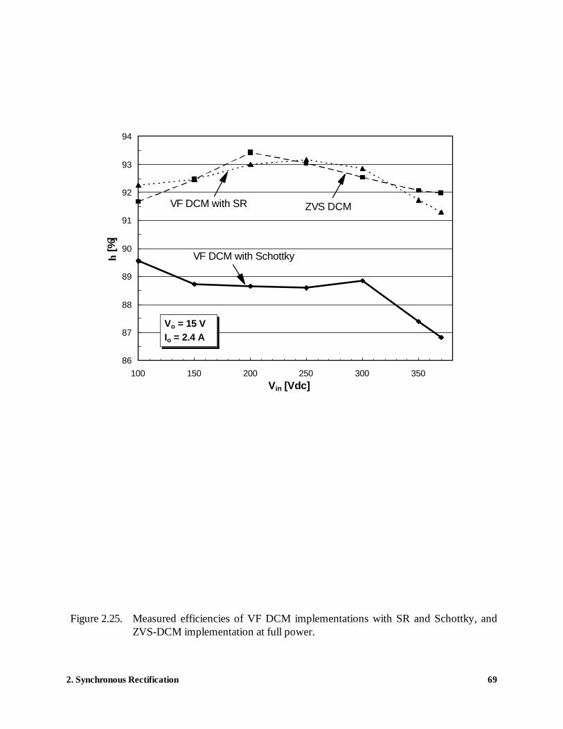
2.23 and 2.25. Furthermore, the efficiency comparisons in Fig. 2.25 shows that VF DCM

2. Synchronous Rectification 68
(a)
(b)
Figure 2.24. Measured waveforms at Vin = 250 Vdc, Vo = 15 V, Io = 2.4 A: (a) VF DCMimplementation with SR; (b) ZVS DCM implementation.
VGS(SW)
I(SR)
VDS(SW)
VGS(SW)
I(SR)
VDS(SW)
Tdelay
Von
TdelayZVS
2. Synchronous Rectification 69
86
87
88
89
90
91
92
93
94
100 150 200 250 300 350Vin [Vdc]
η [%
]
VF DCM with Schottky
VF DCM with SR ZVS DCM
Vo = 15 V Io = 2.4 A
Figure 2.25. Measured efficiencies of VF DCM implementations with SR and Schottky, andZVS-DCM implementation at full power.

2. Synchronous Rectification 70
implementation with the SR has a relatively constant 2.5-4% efficiency improvement over VF
DCM implementation with the Schottky, as has been predicted. However, in the VF DCM
implementation only partial ZVS can be achieved, since in this design, input voltage (Vin = 100-
370 V) is larger than the reflected output voltage (nVo = 95 V), i.e., Vin > nVo.
Soft-switching can be obtained for the entire input line range if secondary current isec is
allowed to flow in the negative direction to the level IZVS given in Eq. (2-20), i.e.,
[ ]I
p
AZVS =⋅ − ⋅
=( : ) ( : )
.38 6 370 386 15
229106
152 2
µ. (2-28)
The required delay time for the secondary current to reach IZVS is
T sdealyZVS = ⋅ =206 15
38 6 150 62
µ µ.( : )
. , (2-29)
as shown in Fig. 2.24(b).
The obtained efficiency of the ZVS DCM converter is very close to that of the VF DCM
converter with the SR due to the increased conduction loss in the ZVS DCM converter. The
switching frequencies of the three VF implementations are shown in Fig. 2.26. Because of the
larger SR output capacitance and additional delay TdelayZVS required to obtain IZVS, VF DCM
converter with the Schottky has the highest switching frequency, while ZVS DCM
implementation has the lowest switching frequency. Also, the switching frequency range in ZVS
DCM implementation is the smallest due to the longest delay time.

2. Synchronous Rectification 71
80
100
120
140
160
180
200
220
100 150 200 250 300 350
Vin [Vdc]
f s [k
Hz]
VF DCM with Schottky
VF DCM with SR
ZVS DCM Vo = 15 V Io = 2.4 A
Figure 2.26. Switching frequency comparison of VF DCM implementations with SR andSchottky, and ZVS-DCM implementation.
2. Synchronous Rectification 72
2.3. Summary
The theoretical efficiency improvement limit of various implementations of synchronous
rectification in flyback converters is presented, as shown in Fig. 2.18. However, unlike
synchronous rectification in forward converter, it is difficult to normalize the efficiency
improvement limit due to its complex dependence on multi-parameters. For general applications
in flyback converters to determine the efficiency improvement of synchronous rectification over
diode rectification, the formulae in Table 2-I, together with Eqs. (2-24) and (2-25), can be used,
once the diode efficiencies are provided or estimated.
It was shown that the variable-frequency (VF) discontinuous-conduction-mode (DCM)
flyback converter implementation is most suitable for synchronous rectification. Moreover, this
implementation can be easily designed to work with complete or partial zero-voltage-switching of
the primary switch by properly adjusting the delay time between the zero-crossing of the
secondary current and the turn-off instant of the synchronous rectifier. In off-line applications,
the VF DCM flyback converter with a synchronous rectifier shows a typical efficiency
improvement in the 2-4% range compared to the corresponding circuit with a diode rectifier.