chapter 2 diode fundamentals dr.debashis de associate professor west bengal university of technology
TRANSCRIPT

Chapter 2
Diode Fundamentals
Dr.Debashis DeAssociate ProfessorWest Bengal University of Technology

Outline
Introduction Formation of the p–n Junction Energy Band Diagrams Concepts of Junction Potential Modes of the p–n Junction Derivation of the I–V Characteristics of a p–n Junction Diode Linear Piecewise Models Breakdown Diode Special Types of p–n Junction Semiconductor Diodes Applications of Diode
INTRODUCTION The origin of a wide range of electronic devices being used can be traced back to a simple device, the p–n junction diode.
The p–n junction diode is formed when a p-type semiconductor impurity is doped on one side and an n-type impurity is doped on the other side of a single crystal.
All the macro effects of electronic devices, i.e., wave shaping, amplifying or regenerative effects, are based on the events occurring at the junction of the p–n device.
Most modern devices are a modification or amalgamation of p–n devices in various forms.
Prior to the era of semiconductor diodes, vacuum tubes were being extensively used. These were bulky, costly and took more time to start conducting because of the thermo-ionic emission.
The semiconductor diodes and the allied junction devices solved all these problems.

FORMATION OF THE p–n JUNCTION
When donor impurities are introduced into one side and acceptors into the other side of a single crystal semiconductor through various sophisticated microelectronic device-fabricating techniques, a p–n junction is formed.
The presence of a concentration gradient between two materials in such intimate contact results in a diffusion of carriers that tends to neutralize this gradient. This process is known as the diffusion process. The nature of the p–n junction so formed may, in general, be of two types:
A step-graded junction:- In a step-graded semiconductor junction, the impurity density in the semiconductor is constant.A linearly-graded junction:- In a linearly-graded junction, the impurity density varies linearly with distance away from the junction.
A semiconductor p–n junction

ENERGY BAND DIAGRAMS The discussion in this section is based on the realistic assumption that a junction is made up of uniformly doped p-type and n-type crystals forming a step-graded junction. The p–n Junction at Thermal Equilibrium
p-type and n-type semiconductors just before contact
From the discussion of the law of mass action, the carrier concentrations on either side away from the junction are given by:
(where pn is the hole concentration in n-type semiconductors, np is the electron concentration in p-type semiconductors; nn and pp are the electron and hole concentrations in n- and p-type semiconductors respectively.)

The energy band diagram of a p–n junction under the condition of thermal equilibrium
Band structure of p–n junction
ENERGY BAND DIAGRAMS

CONCEPTS OF JUNCTION POTENTIAL
Space-charge Region
The non-uniform concentration of holes and electrons at the junction gives rise to a diffusive flow of carriers.
Since the electron density is higher in the n-type crystal than in the p-type crystal, electrons flow from the n-type to the p-type and simultaneously, due to reversibility, the holes flow from the p-type to the n-type.
The result of this migration of carriers is that the region near the junction of the n-type is left with a net positive charge (only ionized donor atoms) while that of the p-type is left with a net negative charge (only ionized acceptor atoms).
This diffusive mechanism of migration of the carriers across the junction creates a region devoid of free carriers, and this region is called the space-charge region, the depletion region or the transition region.

The junction, as noted above, has three major properties:1. There is a space charge and an electric field across the
junction, which in turn indicates that the junction is pre-biased (i.e., there exists a built-in potential, a very important concept, which will be discussed shortly);
2. The impure atoms maintaining the space charge are immobile in the temperature range of interest (at very high temperatures, the impurities become mobile). The pre-biased condition can be maintained indefinitely;
3. The presence of any free electron or hole is strictly forbidden. Built-in and Contact Potentials
This diffusive flow process results in a space-charge region and an electric field.
The resulting diffusion current cannot build up indefinitely because an opposing electric field is created at the junction.
The homogeneous mixing of the two types of carriers cannot occur in the case of charged particles in a p–n junction because of the development of space charge and the associated electric field E0.
CONCEPTS OF JUNCTION POTENTIAL

The electrons diffusing from the n-type to the p-type leave behind uncompensated donor ions in the n-type semiconductor, and the holes leave behind uncompensated acceptors in the p-type semiconductors.
This causes the development of a region of positive space charge near the n-side of the junction and negative space charge near the p-side. The resulting electric field is directed from positive charge towards negative charge.
Thus, E0 is in the direction opposite to that of the diffusion current for each type of carrier.
Therefore, the field creates a drift component of current from n to p, opposing the diffusion component of the current.
Since no net current can flow across the junction at equilibrium, the current density due to the drift of carriers in the E0 field must exactly cancel the current density due to diffusion of carriers.
Moreover, since there can be no net build-up of electrons or holes on either side as a function of time, the drift and diffusion current densities must cancel for each type of carrier.
CONCEPTS OF JUNCTION POTENTIAL

CONCEPTS OF JUNCTION POTENTIAL
Therefore, the electric field E0 builds up to the point where the net current density is zero at equilibrium.
The electric field appears in the transition region of length L about the junction, and there is an equilibrium potential difference V0 across L (known as contact potential).
In the electrostatic potential diagram, there is a gradient in potential in the direction opposite to E0. In accordance with the following fundamental relation:
The contact potential appearing across L under condition of zero external bias is a built-in potential barrier, in that it is necessary for the maintenance of equilibrium at the junction.
It does not imply any external potential. V0 is an equilibrium quantity, and no net current can result from it. In general, the contact potential is the algebraic sum of the built-in potential and the applied voltage. The variations in the contact potential under the condition of applied bias are given in the subsequent sections.

Assuming that the field is confined within the space-charge region L, the potential barrier Vd and the field E0 are related by:
It should be noted that a voltmeter cannot measure this electrostatic potential since the internal field is set up to oppose the diffusion current and also since the built-in potential is cancelled exactly by the potential drop across the contact.
The barrier energy corresponding to barrier potential Vd is expressed as EB = eVd. The value of EB can be changed by doping change. The value of EB is different for different semiconductors.
CONCEPTS OF JUNCTION POTENTIAL

CONCEPTS OF JUNCTION POTENTIAL

CONCEPTS OF JUNCTION POTENTIAL

MODES OF THE p–n JUNCTIONThere are two modes of switching of a p–n junction diode.
Forward-biased p–n junction
When the positive terminal of a battery is connected to the p-type side and the negative terminals to the n-type side of a p–n junction, the junction allows a large current to flow through it due to the low resistance level offered by the junction. In this case the junction is said to be forward biased. Energy band diagram of
Forward-biased p–n junction

Reverse-biased p–n junction
When the terminals of the battery are reversed i.e., when the positive terminal is connected to the n-type side and the negative terminal is connected to the p-type side, the junction allows a very little current to flow through it due to the high resistance level offered by the junction. Under this condition, the p–n junction is said to be reverse-biased.
Energy band diagram of Reverse-biased p–n junction
MODES OF THE p–n JUNCTION

MODES OF THE p–n JUNCTION The p–n Junction with External Applied Voltage
If an external voltage Va is applied across the p–n junction, the height of the potential barrier is either increased or diminished as compared to Va, depending upon the polarity of the applied voltage.The energy band distribution, with applied external voltage, is shown in below figure. For these non-equilibrium conditions, the Fermi level can no longer be identified. In order to describe the behaviour of the p–n junction, quasi- Fermi levels are introduced.

MODES OF THE p–n JUNCTION Rectifying Voltage–Current Characteristics of a p–n Junction
If the polarity of the applied voltage is such that the p-type region is made negative with respect to the n-type, the height of the potential-barrier is increased. Under this reverse-biased condition, it is relatively harder for the majority of the carriers to surmount the potential-barrier. The increase in the potential barrier height is essentially equal to the applied voltage. Under an external applied voltage, the carrier concentrations near the junction are:
(where, the plus and minus signs are for the reverse-biased and the forward-biased conditions.)
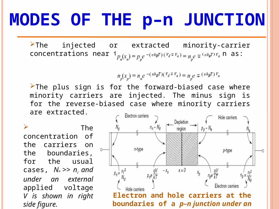
MODES OF THE p–n JUNCTIONThe injected or extracted minority-carrier concentrations near the junction can be written as:
The plus sign is for the forward-biased case where minority carriers are injected. The minus sign is for the reverse-biased case where minority carriers are extracted.
Electron and hole carriers at the boundaries of a p–n junction under an externally applied voltage
The concentration of the carriers on the boundaries, for the usual cases, Na >> ni and under an external applied voltage V is shown in right side figure.

MODES OF THE p–n JUNCTION
The profiles of charge density, potential, and electric field in an abrupt junction

MODES OF THE p–n JUNCTION
The schematic diagram of the varactor diode
The doping profiles used in varactor diode

DERIVATION OF THE I–V CHARACTERISTICS OF A p–n
JUNCTION DIODE Let us consider the fact that the drift component of the current is negligible. Then from continuity equation, we can write:
where, Lp = √Dpτp is the diffusion length and pn is the equilibrium density of holes in the n-region far away from the junction.The solution of the ordinary differential is:
where, C1 and C2 are two arbitrary constants. The boundary conditions in this case are:
From above two equation we get C2 = 0 and
DERIVATION OF THE I–V CHARACTERISTICS OF A p–n
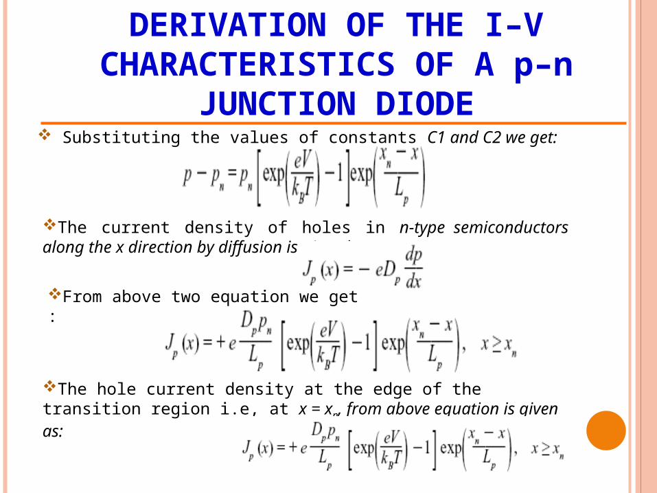
JUNCTION DIODE Substituting the values of constants C1 and C2 we get:
The current density of holes in n-type semiconductors along the x direction by diffusion is given by:
From above two equation we get :
The hole current density at the edge of the transition region i.e, at x = xn, from above equation is given as:

The hole current density at the edge of the transition region i.e, at x = xp, from above equation is given as:
DERIVATION OF THE I–V CHARACTERISTICS OF A p–n
JUNCTION DIODE
The total diode-current density is given by:
The total direct current of the diode, with a cross-sectional junction area A, is:
where

DERIVATION OF THE I–V CHARACTERISTICS OF A p–n
JUNCTION DIODE
Actual and theoretical I–V characteristics of a typical semiconductor diode
The plot of the voltage–current characteristics of the diode, for forward-bias and reverse-bias, is shown below.It should be noted that because of the higher concentration of holes in the p-region the hole current is much larger than the electron current.

LINEAR PIECEWISE MODELS The p–n junctions are unilateral in nature, i.e., they conduct current in only one direction. Thus, we can consider an ideal diode as a short circuit when forward-biased and as an open circuit when reverse-biased. Forward biased diodes exhibit an offset voltage (Vy) that can be approximated by the simple equivalent circuit with a battery in series with an ideal diode. The series battery in the model keeps the ideal diode turned off for applied voltage less than V; the actual diode characteristic is improved by adding a series resistance (r) to the equivalent circuit. The equivalent diode model, is called the piecewise linear equivalent model.
Linear piecewise models of a diode for different order of approximations
I–V Characteristics of p–n junction diode

BREAKDOWN DIODE
Breakdown diodes are p–n junction diodes operated in the reverse-bias mode. This breakdown occurs at a critical reverse-bias voltage (Vbr). At this critical voltage the reverse current through the diode increases sharply, and relatively large currents flow with little increase in voltage. These diodes are designed with sufficient power-dissipation capabilities to work in the breakdown region. The following two mechanisms can cause reverse breakdown in a junction diode.
Reverse-biased p–n junctionReverse breakdown in a p–n junction

BREAKDOWN DIODE Zener Breakdown
Zener breakdown occurs when a sufficiently large reverse-bias is applied across a p–n junction diode. The resulting electric field at the junction imparts a very large force on a bound electron, enough to dislodge it from its covalent bond. The breaking of the covalent bonds produces a large number of EHP (electron–hole pairs). Consequently the reverse current becomes very large. This type of breakdown phenomena is known as Zener breakdown.
Energy band diagram of a Zener
diode
Reverse bias with electron tunnelling from p to n
leads to Zener breakdown I–V characteristics

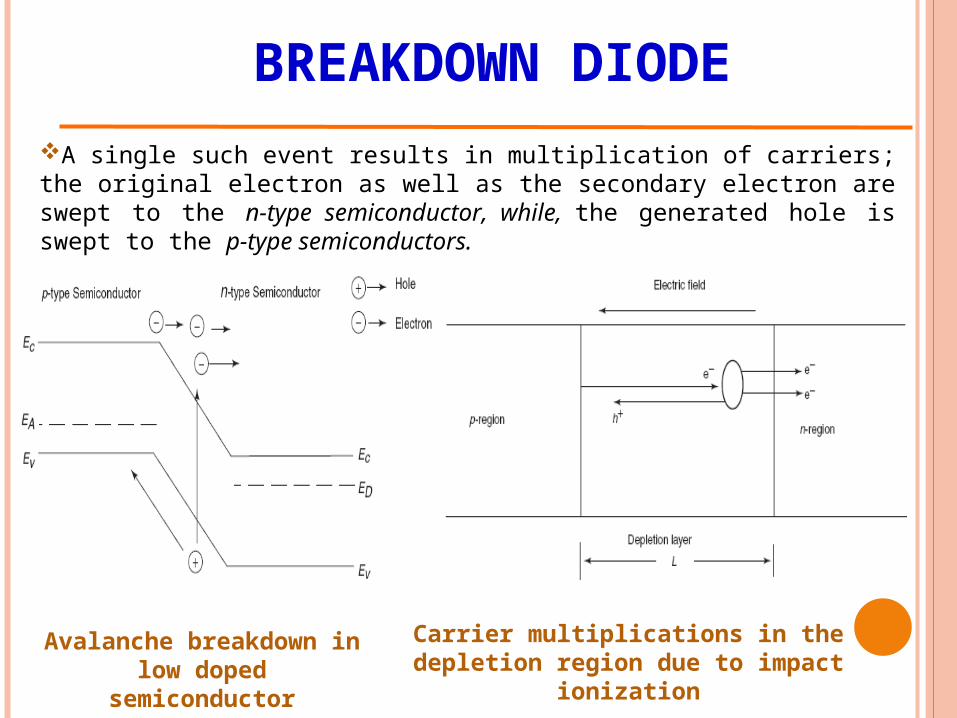
BREAKDOWN DIODE Avalanche Breakdown
In a reverse-biased junction, the minority-carriers drift across the depletion region. On their way across this region, they occasionally have collisions with atoms in the lattice. With a large enough field, a carrier drifting across the depletion region is accelerated to the point where it has enough energy to knock a valance electron free from its host atom during a collision. The field then separates the electron and hole of this newly created EHP and we now have three mobile carriers instead of one. This process is called avalanche multiplication. The multiplication can become quite large if the carriers generated by this collision also acquire to create more carriers, thereby initiating a chain reaction. Once the process starts, the number of multiplication that can occur from a single collision increases rapidly with further increase in the reverse-bias, so the terminal current grows rapidly, and we say that the junction breaks down. This is called avalanche breakdown.
BREAKDOWN DIODE
Avalanche breakdown in low doped semiconductor
A single such event results in multiplication of carriers; the original electron as well as the secondary electron are swept to the n-type semiconductor, while, the generated hole is swept to the p-type semiconductors.
Carrier multiplications in the depletion region due to impact ionization

BREAKDOWN DIODE Comparison between Zener and avalanche breakdown
The I–V characteristics comparison between Zener and avalanche breakdown
Comparison of Zener breakdown of Ge and Si semiconductor diodes with respect
to I–V curve

SPECIAL TYPES OF p–n JUNCTION SEMICONDUCTOR DIODES
Tunnel Diode The tunnel diode is a negative-resistance semiconductor p–n junction diode. The negative resistance is created by the tunnel effect of the electrons in the p–n junction as already discussed in the section of Zener diode.
Tunnel diode under zero bias equilibrium Small reverse bias

The doping of both the p- and n-type regions of the tunnel diode is very high—impurity concentration of 1019 to 1020 atoms/cm3 are used (which means both n-type and p-type semiconductors having parabolic energy bands are highly degenerate)—and the depletion layer barrier at the junction is very thin, in the order of 10-6cm.
SPECIAL TYPES OF p–n JUNCTION SEMICONDUCTOR DIODES
Small forward biasIncreased forward bias
Increased forward bias condition where the
current begins to increase again

SPECIAL TYPES OF p–n JUNCTION SEMICONDUCTOR DIODES
Small-signal model of the tunnel diode. (Typical values for these parameters for a tunnel diode of peak current IP 10 mA
are –Rn – 30 Ω, Rs 1 Ω, Ls 5 nH and capacitance C 20 pF respectively)
I–V characteristics of a tunnel diode
Symbol of tunnel diode

SPECIAL TYPES OF p–n JUNCTION SEMICONDUCTOR DIODES
Light-emitting Diode Charge carriers recombination takes place at the p–n junction as electron crosses from the n-side and recombines with holes on the p-side. When the junction is forward-biased the free electron is in the conduction band and is at a higher energy level than the hole located at valence band. The recombination process involves radiation of energy in the form of photons. If the semiconductor material is translucent, the light will be emitted and the junction becomes a light source, i.e., a light-emitting diode (LED). LEDs are p–n junctions that can emit spontaneous radiation in ultraviolet, visible, or infrared regions. Advantages of LEDs1. Low operating voltage, current and power consumption make LEDs compatible with electronic drive circuits.2. LEDs exhibit high resistance to mechanical shock and vibration and allow them to be used in severe environment conditions.3. LEDs ensure a longer operating life line, thereby improving the overall reliability and lowering the maintenance costs of equipment.

SPECIAL TYPES OF p–n JUNCTION SEMICONDUCTOR DIODES
4. LEDs have low inherent noise levels and also high immunity to externally generated noise.
5. LEDs exhibit linearity of radiant power output with forward current over a wide range.
Limitations of LEDs1. Temperature dependence of radiant output power and wavelength.2. Sensitivity to damages by over voltage or over current.3. Theoretical overall efficiency is not achieved except in special
cooled or pulsed conditions.
(a) Schematic showing the basic process of absorption (b) emission The symbol of an LED

SPECIAL TYPES OF p–n JUNCTION SEMICONDUCTOR DIODES
Photovoltaic DiodeThe photovoltaic diode or solar cell is an important technological device for overcoming energy problems. It is also known as solar energy converter; it is basically a p–n junction diode which converts solar energy into electrical energy. The energy reaching the earth’s surface from the sun is primarily electromagnetic radiation, which covers a spectral range of 0.2 to 0.3 micrometre. The conversion of this energy into electrical energy is called photoelectric effect.
Construction and working principle A photovoltaic diode essentially consists of a silicon p–n junction diode usually packaged with a glass window on the top. Surface layer of the p-material is made extremely thin so that the incident light (photons) can penetrate and reach the p–n junction easily.

SPECIAL TYPES OF p–n JUNCTION SEMICONDUCTOR DIODES
When these photons collide with the valence electrons, they impart in them sufficient energy so that they gain enough energy to leave the parent atoms. In this way, free electrons and holes are generated on both sides of the junction. Consequently, their flow constitutes a current (minority current). This current is directly proportional to the illumination (lumen/m2 or mW/m2). This, in general depends on the size of the surface being illuminated. The open circuit voltage Voc is a function of illumination. Consequently, power output of a solar cell depends on the level of sunlight illumination. Power cells are also available in the form of a flat strip so as to cover sufficiently large surface areas.
Structure of a solar cell

SPECIAL TYPES OF p–n JUNCTION SEMICONDUCTOR DIODES
I–V characteristics of an illuminated solar cell showing the point of maximum power
Top finger contact with anti-reflecting coating
Current–voltage characteristics It is seen that the curve passes through the fourth quadrant and hence the device can deliver power from the curve. The power delivered by the device can be maximized by maximizing the area under the curve or by maximizing the product (Isc Voc). By properly choosing the load resistor, output power can be achieved. In the absence of light, thermally generated minority carriers across the junction constitute the reverse saturation current.
APPLICATIONS OF DIODE
Radio Demodulation:- In demodulation of amplitude modulated (AM) radio broadcasts diodes are used. The crystal diodes rectify the AM signal, leaving a signal whose average amplitude is the desired audio signal. The average value is obtained by using a simple filter and the signal is fed into an audio transducer, which generates sound. Power Conversion:- In the Cockcroft–Walton voltage multiplier, which converts ac into very high dc voltages, diodes are used. Full-wave rectifiers are made using diodes, to convert alternating current electricity into direct current . Over-voltage Protection:- Diodes are used to conduct damaging high voltages away from sensitive electronic devices by putting them in reverse-biased condition under normal circumstances. When the voltage rises from normal range, the diodes become forward-biased (conducting). In stepper motor, H-bridge motor controller and relay circuit’s diodes are used to de-energize coils rapidly without damaging voltage spikes that would otherwise occur. These are called a fly-back diodes. Logic Gates:- AND and OR logic gates are constructed using diodes in combination with other components. This is called diode logic.

Ionizing Radiation Detectors In addition to light, energetic radiation also excites semiconductor diodes. A single particle of radiation, having very high electron volts of energy, generates many charge carrier pairs, as its energy is transmitted in the semiconductor material. If the depletion layer is large enough to catch the whole energy or to stop a heavy particle, an accurate measurement of the particle’s energy is possible. These semiconductor radiation detectors require efficient charge collection and low leakage current. They are cooled by liquid nitrogen. Common materials are Ge and Si.
Temperature Measuring:- The forward voltage drop across the diode depends on temperature. A diode can be used as a temperature measuring device. This temperature dependence follows from the Shockley ideal diode equation and is typically around -2.2 mV per degree Celsius. Charge-coupled Devices:- Arrays of photodiode, integrated with readout circuitry are used in digital cameras and similar units.
APPLICATIONS OF DIODE