diode and applications of diode
TRANSCRIPT

Welcome to Our Presentation
GROUP MEMBERMOIN SHOBUJ : 143-33-2194
NAZMUR SHAKIB : 151-33-2474
MOFAZZAL HOSSEN : 152-33-2623
MAHMUDUL HASAN : 152-33-2683
REZOWAN HAMID : 143-33-2297
NEAOUS SHARIF : 152-33-2690
MOSLAMIN SIKDER : 152-33-2715
MD.RASEDUL HASAN : 152-33-2667

Diode And Applications Of Diode
Content
Diode
The construction and Symbol of Diode
Depletion Region and Junction Voltage
Diode I/V Characteristic
Application

Diode
In electronics, a diode is a two-terminal electronic component that conducts primarily in
one direction.
it has low resistance to the flow of current in one direction, and high resistance in the other.
The discovery of crystals' rectifying abilities was made by German physicist Ferdinand
Braun in 1874. The first semiconductor diodes, called cat's whisker diodes, developed
around 1906
Today, most diodes are made of silicon, but other semiconductors such as selenium

The construction and Symbol of Diode
Made form a combination of 2 extrinsic semiconductor p-type and n-type material.
The joint between the p- type n-type material is called p n junction.
Have two terminal (anode and cathode).

Types of semiconductor Diode
Cat's whisker or crystal diodes: Cat's whisker diodes were also called crystal diodes and found application in the earliest radios called crystal radio receivers. Cat's whisker diodes are generally obsolete, but may be available from a few manufacturers.
Zener diodes : These can be made to conduct in reverse bias (backward), and are correctly termed reverse breakdown diodes. This effect, called Zener breakdown, occurs at a precisely defined voltage, allowing the diode to be used as a precision voltage reference.
Thermal diodes: This term is used both for conventional p–n diodes used to monitor temperature because of their varying forward voltage with temperature, and for Peltier heat pumps for thermoelectric heating and cooling.
Power diode: Rectifying power supply circuit .

Power diode: Rectifying power supply circuit .
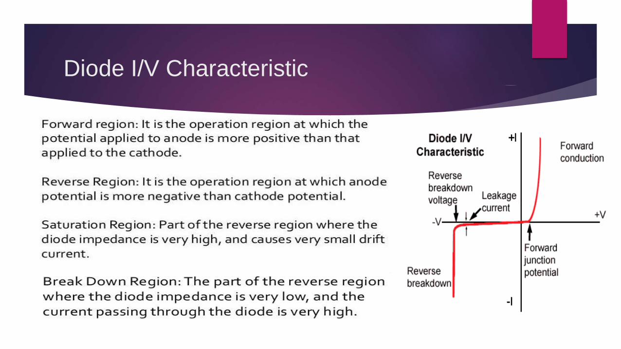
Diode I/V Characteristic

Depletion Region and Junction Voltage
At p n junction electrons from the n type semi conductor will be
attracted to the hole in the p type semiconductor.
As a result the holes and the electron at the p n junction disappear
forming a layer called depilation layer.
At the same time the p type semiconductor become more negative
whirs the n type semiconductor become more positive.
this will result potential difference across the p n junction .this potential
difference called the junction voltage.

Application
Half wave Rectifier
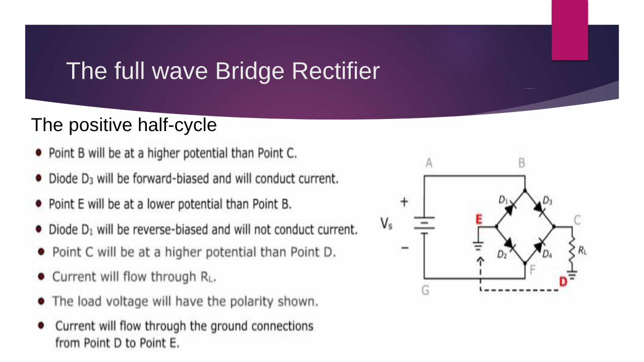
The full wave Bridge Rectifier
The positive half-cycle
.

The full wave Bridge Rectifier
The Negative half-cycle Prints F and E will be at higher potential
than print C and B.
Diode D4 and D1 will be forward biased
and current will conduct.

The full wave Bridge Rectifier

The full wave Rectifier and Capacitor Filter

Thanks to All