chapter 19 high-speed signaling - web.stanford.edu · chapter 19 high-speed signaling advances in...
TRANSCRIPT

1
Chapter 19
High-Speed SignalingAdvances in IC fabrication technology coupled with aggressive circuit design have led to an
exponential growth in the speed and integration levels of digital IC’s. This has in turn created a
great demand for high-speed links and busses to interconnect these chips. Gbit/s-scale I/O’s are
being adopted for memory busses [28], peripheral connections [31], and multiprocessor
interconnection networks [16]. This chapter looks at these high-speed links and discusses
important design issues and current design techniques.
The design of a link would be very simple if only the speed of light were infinite1 since then an
inverter would be a perfect driver and receiver. Finite speed of light, however, makes the design
much more difficult. The link electronics must deal with the time delay of the information
travelling down the wire and the signal energy stored on the wire. (The power driven into the wire
takes time to reach the load.) To deal with these issues, a high-speed link has four parts: a
transmitter that converts the bits to an electrical signal capable of propagating on a long wire, the
long wire itself, a receiver that converts the signal energy of the wire back to bits, and a timing-
recovery circuit that compensates for the time delay of the wire. Figure 1 illustrates these
components.
1. For most IC circuit design (and most of the designs in this book), this assumption is in fact made. Short wires are modelled as a ‘node’ and only has lumped capacitance, and long wires are modelled by a distributed RC network. This approximation is valid, since the time of flight of the signal on the wire is very small compared to the frequency of interest (i.e. the circuit is much smaller than the wavelengths of interest). To model finite signal velocity, the wire must be a distributed RLC network as described in the next section
Figure 1: Signaling system components
ReceiverTransmitter
Channel
TimingRecovery
Data out Data in
1001 1001

2 Chapter 19: High-Speed Signaling
The next section briefly reviews the electrical issues associated with transmission lines, the
common name for these long wires, and describes how different wire configurations affect the
noise in the system. Section 19.2 discusses metrics often used to assess the performance of I/O
interfaces and describes how the timing and voltage margins are used to measure the robustness of
a link. Using these metrics, we will then examine each link component, beginning with the
transmitter (Section 19.3) continuing with the receiver (Section 19.4) and the timing-recovery
circuits (Section 19.5) and ending with the limitations caused by the transmission line, and what
can be done about them in Section 19.6.
19.1 Transmission LinesWhen the transmitter starts driving a transmission line, it launches an electromagnetic wave. This
wave can only ‘see’ the initial part of the transmission line; it has no information about the final
load or even other segments of the wire. So, the geometry and materials of this local segment set
the ratio of the signal’s voltage to its current. This ratio is called the line impedance since it has
the same dimensions (V/I) as resistance. An ideal transmission line can be modeled as a
distributed LC circuit, where the inductance and capacitance model the stored magnetic and
electric energy of the wave. The impedance of the line is set by and signals propagate
with a velocity of where L and C are the inductance and capacitance per unit length.
A simple model of a transmission line is shown in Figure 2 where the distributed line has been
approximated by a number of LC sections.
19.1.1 Image Currents
A critical property of transmission lines is that they are intrinsically differential structures, i.e.
each port really has two terminals, the signal and its return. When one launches a current into the
transmission line, an equal and opposite current, called the image current, starts to flow out the
Figure 2: Simple transmission-line model. The first model shows the inductance in both the signal and return paths with strong mutual coupling between the two. Since the current in the return is always equal and opposite to the signal current, the rightmost model is equivalent for modeling the signal difference between the terminals.
L
CT-Line
C
L/2+M
L/2+M
M
Z L C⁄=
v 1 LC( )⁄=

19.1 Transmission Lines 3
return. The right-most circuit in Figure 2 only models the differential signal between the pins of
each port and not any common-mode signal; the two return pins are not actually shorted together.
Since the return is often connected to an AC ground, many designers forget about the image
current and the return path, but return path errors are the most common causes of link noise.
Some transmission line environments such as coaxial cables provide good signal returns. Printed
circuit boards (PCBs) can also be built to provide a good transmission-line environment by
placing reference planes (ground or VDD) under each wiring layer, forming microstrip lines.2
Absence of an explicit signal return in the vicinity of the signal trace will result in the image
current flowing on other signal traces. This coupling between signals gives rise to crosstalk and is
modeled by coupling capacitance and mutual inductance between the wires. The worst
transmission line environment often exists in IC packages. Since common packages do not
employ ground-planes and the connections for the image currents are far from the signals,
excessive coupling (cross-talk) can arise between the signal lines.3
Crosstalk creates noise on the victim wire that is proportional to the signal on the aggressor wire.
Since coupling is through a frequency dependent reactance (ωL and 1/ωC), the proportionality
constant depends on the bandwidth of the signals. As will be discussed in Section 19.3.2, signals
with energy at high frequencies (i.e. fast edge rates) experience greater amounts of coupling,
creating the need to limit the transmitted signal bandwidth.
19.1.2 Reflections
Another source of proportional noise is impedance mismatch in the transmission line which
causes reflections. The long wires that the transmitter must drive often consist of a number of
different sections -- a wire on the package connecting the transmitter chip and the printed circuit
board (PCB), a trace on the PCB, possibly connectors and a coaxial or twisted-pair cable between
2. However, some thought about the image currents must be given in PCB layout since when a signal line changes wiring levels through a via the image current must change levels. If a high-speed bus changes levels, the two image planes must be connected or well bypassed to allow the image current to change levels as well. If the image planes are not bypassed, AC noise will appear between the two return planes. This noise will then change the voltage difference between the signal and the plane on the second level, and will look like noise at the other end of the signal trace.
3. Even with advanced flip-chip, ball-grid packages, traces are needed to fanout the bumps and balls to vias on the package and board. Coupling in these traces can still be an issue.
4 Chapter 19: High-Speed Signaling
boards, a trace on the receiving PCB, and another package wire to connect to the receiver chip.
Each connection between transmission line segments must satisfy both constraints of
conservation of energy and continuity of voltage, i.e: (i) power flowing into the connection has to
be equal to the power flowing out of it, and (ii) the voltages at the two sides of the connection
have to be equal. If the connected impedances are the same, the solution is trivial, and the signal
flow continues with the same voltage. If the second segment has a lower impedance, the voltage
in this segment has to be lower (equal or higher voltage would mean that the connection generates
power). So, in order to reduce the voltage and increase the current flowing towards the second
segment a negative wave is created and sent back to the transmitter. This way the superposition of
the forward and backward waves in the first segment match the current and voltage of the forward
travelling wave in the second segment. Conversely, if the impedance of the second segment is
larger, the voltage in this segment is larger, and to balance the voltage and reduce the current, the
reflected wave is positive.4 These constraints lead to the familiar equation for the reflection size,
, where Γ is the reflection coefficient.
Reflections can be viewed as feedback signals indicating that the current-to-voltage ratio
established at the transmitter is incorrect and needs to be adjusted. However, since no information
about the transmitter impedance is available at the reflection-generating connection, a few round
trips might occur before the system settles. At that point the voltage and current in all segments of
the transmission line will be uniform, and the ratio (V/I) is set by the final load impedance. If the
wire delay is very small compared to the rise time of the signal, this settling happens so quickly
that the driver essentially sees the load directly, and reflections can be ignored because they are
very brief compared to the signal transition.
Reflections in high-speed links can degrade performance. They are versions of the transmitted
signal that arrive at the receiver after spending some time traveling in the wrong direction on the
transmission line and hence have a different delay. Since they arrive out-of-sync with the main
signal, the reflections appear as noise at the receiver.5
4. Even in cases where the reflected waves are of reasonable amplitude, e.g., 20%, most of the signal power continues down the line (reflected power is only 4% in this case). Thus even if the segments are not at the right impedance, the effect on the signal amplitude at the end of line is usually small.
Vreflect ΓVin
Zout Zin–
Zout Zin+------------------------Vin= =

19.1 Transmission Lines 5
Connecting a transmission line to a driver or receiver is just like connecting it to another segment
of a transmission line. If the impedances do not match, a reflection will occur. Sometimes systems
are intentionally designed with a mismatched impedance at either the driver or receiver. Systems
are built with low-impedance drivers that guarantee a certain voltage swing is driven on the wire.
In these systems, the receiver is built to match the impedance of the wire to prevent reflections.
Similarly, many systems are built where the transmitter’s impedance is matched to the line, and
the receiver is left unterminated (high-impedance). In these systems, a wave of half the desired
signal is launched in the wire (with the driver and transmission line forming a Zo/(Zdrv+Zo)
voltage divider). This voltage doubles when it reflects at the open end of the transmission line,
presenting a full-swing signal at the receiver. The reflected wave is then absorbed when it reaches
the driver. The advantage of this source-terminated system is that it does not dissipate any static
power. Once the wave reflects back at the driver, the net current in the line goes to zero.
Systems where either the driver or receiver is intentionally mismatched to the transmission line
impedance require better impedance control of the transmission-line segments than a system
where both the transmitter and receiver are terminated. For a reflection to interfere with the
received signal, a signal must be reflected an even number of times (each reflection changes the
signal direction). Thus the reflection noise interfering with the received signal will be
proportional to the product of the two worst reflection coefficients in the system, including the
reflections at the driver and the receiver. For reasonable impedance control ( % reflections),
double termination reduces the reflection noise at the receiver to around % from around %
for a system with either end unterminated.
19.1.3 Attenuation
An ideal transmission-line segment simply delays the input signal without inducing any distortion
of its spectral characteristics. However, real transmission media attenuate the signal because of
the line conductor’s resistance and the loss in the dielectric between the conductors. Both loss
mechanisms increase with increasing signal frequency, causing the wires to behave as low-pass
5. Actually, reflected signals are not true noise because they are predictable and can be compensated out. Systems that ‘equalize’ the channel do exactly that, by computing the extra delay of the reflection, and subtracting it from the received signal.
10±
1± 10±
6 Chapter 19: High-Speed Signaling
filters. Longer wires result in more severe filtering. The filtering of the line reduces the amplitude
of a bit and spreads the signal out in time, adding a tail that interferes with subsequent bits.
While high-frequency loss has recently become an issue in high-speed link design, the sections on
link components will focus on performance limits of the silicon circuits rather than the wires.
After discussing the capabilities of the silicon, Section 19.6 describes high-frequency wire loss in
more detail and proposes different ways to deal with the problem. Many of these approaches are
system solutions that leverage the information presented in the previous sections.
19.1.4 Methods of Signaling
The characteristics of transmission lines, described in the previous section, make it easier to
understand the trade-offs between different signaling topologies. In general, three largely
independent binary choices characterize most signaling systems: point-to-point link or multi-drop
bus, unidirectional or bidirectional link, and single-ended or differential signaling. The latter two
choices are a trade-off between wires and proportional noise in the system.
In applications that require low-latency between multiple ports such as DRAMs and backplanes,
multi-drop busses have been preferred over point-to-point connections. Point-to-point structures
require either more routing in a fully-connected network or induce larger latency in a daisy-chain
connection. However, the electrical characteristics of busses are considerably worse than point-to-
point links. Each drop of the bus appears as a short line splitting off from the transmission line,
causing the propagating energy to divide and then reflect off the unterminated end. Unless the
stub is very short, e.g. in a Rambus system [28], making busses work at high speeds is extremely
difficult. So in the subsequent sections of this chapter the discussion on high-performance I/O
circuits will be directed towards point-to-point links.
Another cost/performance trade-off is whether the system is unidirectional or bidirectional. For
bidirectional links, each pin is attached to both a transmitter and a receiver. Typically, only one
transmitter-receiver pair in a link is operating at one time (half duplex), halving the system
bandwidth. An alternative is simultaneous bidirectional links (full duplex) which can achieve low
pin count and high aggregate bandwidth but requires much more careful design. The receiver
must cancel out its own transmitted signal, and a single reflection of the transmitted signal will act

19.2 Link Performance Metrics 7
as noise seen by its own receiver. Thus, simultaneous bidirectional signaling decreases the
number of signaling wires at the cost of an increase in self-generated noise.
A similar trade-off between pin-count and performance is present in differential versus single-
ended signaling. Differential signaling requires two connections. In the ideal case, each signal
serves as the other’s return path, and all of the signal energy is stored between the two wires. This
situation is the case for a perfect differential medium, such as a twisted pair suspended in space. In
actuality, many implementations (e.g., in a PC-board environment) couple the two signals to a
common ground plane. The effect is that the net image current in the ground plane is zero. While
single-ended signals also use two connections, the return path is often connected to a supply and
is shared to reduce pins. The sharing of the return current path increases coupling between the
signals, which increases the noise on these signals.
Section 19.3 and Section 19.4 discuss how the different signaling methods interact with the
transmitter and receiver circuit design. Before starting that discussion we will briefly digress and
talk about different methods of measuring both CMOS circuit performance and overall link
performance.
19.2 Link Performance MetricsTo understand the basic frequency limitations in high-speed links and how they will scale with
technology, this section presents a delay metric that, to the first order, uncouples circuit
performance from fabrication technology. This metric helps identify the clock frequency as one of
the major limitations to simple CMOS link speeds. Next it presents the ‘eye’ diagram, which
overlays the transmitted waveforms of a long series of bits on top of each other to better illustrate
the link margins. Using this diagram, it is easy to see how coupling, reflections and filtering
reduce the margin of the link. In addition to the deterministic noise that we have discussed so far,
there is also true statistical noise in the system. If the margin after the deterministic noise is not
large enough, the true noise will cause random bit errors, leading to a measurable bit error rate
(BER) for the link.
8 Chapter 19: High-Speed Signaling
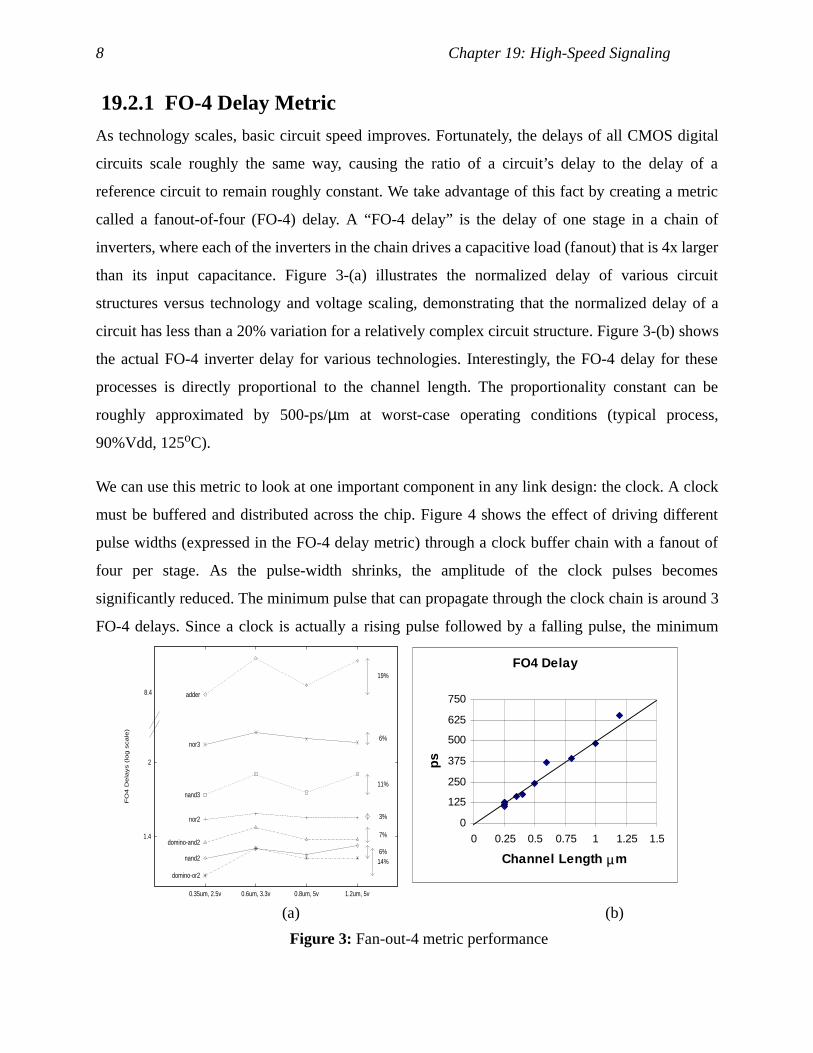
19.2.1 FO-4 Delay Metric
As technology scales, basic circuit speed improves. Fortunately, the delays of all CMOS digital
circuits scale roughly the same way, causing the ratio of a circuit’s delay to the delay of a
reference circuit to remain roughly constant. We take advantage of this fact by creating a metric
called a fanout-of-four (FO-4) delay. A “FO-4 delay” is the delay of one stage in a chain of
inverters, where each of the inverters in the chain drives a capacitive load (fanout) that is 4x larger
than its input capacitance. Figure 3-(a) illustrates the normalized delay of various circuit
structures versus technology and voltage scaling, demonstrating that the normalized delay of a
circuit has less than a 20% variation for a relatively complex circuit structure. Figure 3-(b) shows
the actual FO-4 inverter delay for various technologies. Interestingly, the FO-4 delay for these
processes is directly proportional to the channel length. The proportionality constant can be
roughly approximated by 500-ps/µm at worst-case operating conditions (typical process,
90%Vdd, 125oC).
We can use this metric to look at one important component in any link design: the clock. A clock
must be buffered and distributed across the chip. Figure 4 shows the effect of driving different
pulse widths (expressed in the FO-4 delay metric) through a clock buffer chain with a fanout of
four per stage. As the pulse-width shrinks, the amplitude of the clock pulses becomes
significantly reduced. The minimum pulse that can propagate through the clock chain is around 3
FO-4 delays. Since a clock is actually a rising pulse followed by a falling pulse, the minimum
Figure 3: Fan-out-4 metric performance
(a) (b)
1.4
2
0.35um, 2.5v 0.6um, 3.3v 0.8um, 5v 1.2um, 5v
FO
4 D
ela
ys (
log s
cale
)
domino-or2
domino-and2
nand2
nor2
nand3
nor3
adder8.4
19%
6%
3%
11%
6%
7%
14%
FO4 Delay
0
125
250
375
500
625
750
0 0.25 0.5 0.75 1 1.25 1.5
Channel Length µm
ps

19.2 Link Performance Metrics 9
clock cycle time will be 6 FO-4. Accounting for margins, clocks cycles faster than 8 FO-4 (which
is roughly 2x the frequency of the clock in Alpha microprocessors) are unlikely. However, this
clock limitation leads to relatively low data rates (500-Mb/s in a 0.5-µm technology). High-speed
transmitters and receivers will need to transmit more than one bit per clock cycle by using
parallel-to-serial and serial-to-parallel converters.
19.2.2 Link Margins
To understand how many bits per cycle can be transmitted, we can create an ‘eye’ diagram, a plot
that quickly shows the voltage and timing margins of a link. An example of this plot is illustrated
in Figure 5. If reflections or other proportional noise are present, the voltage of a ‘1’ and ‘0’
becomes uncertain since its value depends on the noise. The voltage margin, the difference
Figure 4: Pulse amplitude at the end of a chain of 4 FO-4 inverters as a function of pulse width.
2.5 3.5 4.5 5.50.0
10.0
20.0
30.0
40.0
50.0
60.0
Clock pulse width (FO-4)
Pul
se a
mpl
itude
red
uctio
n (%
)
Figure 5: Eye diagram of transmitter output.
bit stream
overlay of bits eye diagram with 15-% reflections

10 Chapter 19: High-Speed Signaling
between the highest ‘0’ and the lowest ‘1’, becomes smaller as can be seen by the reduction of the
eye height. Voltage noise also decreases the eye width because of the signal’s finite slope.
Eye diagrams are also a good way to look at the effect of low-pass filtering on a link. As shown in
Figure 6, due to filtering, a reduction in bit time results in a pulse amplitude reduction. Low-pass
filtering also causes intersymbol interference (ISI), since the tail of the previous bit affects the
starting voltage of the current bit thus introducing uncertainty in the amplitude and reducing the
timing margins. The eye closes completely and the signal is undetectable when an isolated pulse
is attenuated by a factor of 2 (6dB).
Generally, eye diagrams are shown for signals at the receiver’s input. Since the receiver has
internal noise sources, a designer measures the true link margins by adding both timing and
voltage offsets at the receiver and then measuring how much can be added before the link starts to
fail. Rather than always tracing the complete eye diagram, often one estimates the eye by
measuring the voltage and timing margins at the center of the eye.
So far we have described deterministic noise sources which are due to the ISI and reflections of
the transmitted signal or coupling from other signals in the system. In addition to this self-
generated noise, there is true gaussian noise as well. While techniques exist to correct for self-
Figure 6: Reduction of data-eye due to simple RC low-pass filter. The bit width is mea-sured in number of time constants. The ISI becomes large for bits smaller than 2 RC.
4RC 2.5RC
2RC 1.2RC
Vol
tage
Time
19.3 Transmitters 11
generated noise (e.g., equalization that will be discussed in Section 19.6), the random noise is not
correctable, and sets a limit on system performance. The intrinsic sources of this noise are the
random fluctuations due to the inherent thermal and shot noise of the system components. For
links operating with small voltage or timing margins, the random noise will occasionally cause
the link to fail. To account for this, links often specify a bit error rate (BER) which is the
probability that any bit will be in error. For example, a 1 Gbps link with a BER of 10-11 will fail
on average every 100 seconds or once in 1011 bits. The probability of failure is an exponential
function of the excess signal margin (signal minus proportional noise) divided by the RMS value
of the noise. Since the RMS noise of most links is small (on the order of millivolts) changing the
true signal margins by 10-20mV can change the BER by many orders of magnitude.
The next sections will use these metrics to look at circuit techniques for building high-speed, low-
noise transmitters and receivers.
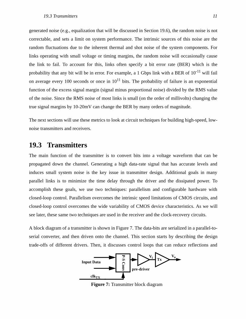
19.3 TransmittersThe main function of the transmitter is to convert bits into a voltage waveform that can be
propagated down the channel. Generating a high data-rate signal that has accurate levels and
induces small system noise is the key issue in transmitter design. Additional goals in many
parallel links is to minimize the time delay through the driver and the dissipated power. To
accomplish these goals, we use two techniques: parallelism and configurable hardware with
closed-loop control. Parallelism overcomes the intrinsic speed limitations of CMOS circuits, and
closed-loop control overcomes the wide variability of CMOS device characteristics. As we will
see later, these same two techniques are used in the receiver and the clock-recovery circuits.
A block diagram of a transmitter is shown in Figure 7. The data-bits are serialized in a parallel-to-
serial converter, and then driven onto the channel. This section starts by describing the design
trade-offs of different drivers. Then, it discusses control loops that can reduce reflections and
Figure 7: Transmitter block diagram
Tx
clkTX
pre-driver
VoVi
P-S
Conv
Input Data

12 Chapter 19: High-Speed Signaling
signal coupling, and maintain accurate output levels. The last part of this section talks about using
parallelism to improve the bit rate of the link.
19.3.1 Output Drivers
There is not much variability in the design of transmitter output drivers. They consist of one or
two transistors and possibly one resistor. The two main variables are the impedance of the driver
and the operating region of the MOS device. A voltage-mode driver consists of two transistors
which connect to supplies that set the signal swing. The transistors are sized so they operate in the
linear region of their I-V curve. This type of driver can be used as a low-impedance driver. By
correctly sizing transistors and possibly adding a series resistor, the driver’s source impedance can
be designed to match the impedance of the line (Figure 8-(a) and (b)). A special low-voltage
supply is often used with this type of driver to reduce the voltage swing and hence the power
needed to drive the transmission line. Signal swings under a volt are common, and for these low
voltages the pMOS pull-up transistor is replaced by an nMOS device. A current-mode driver
(Figure 8-(c)) generally contains a single transistor that operates in the saturation region of the I-V
curve. This driver can act as a high-impedance driver, or by adding a parallel termination
resistance, it can be a matched-impedance driver as well.
Very low-impedance voltage-mode drivers are sometimes built [12] but they are usually not
needed. The reason is that they require large transistors to get the low (~5Ω) desired resistance,
and this low impedance drive causes reflections. Most voltage-mode drivers are matched to the
line impedance to minimize reflections. This can be done by adjusting the size of the devices to
match the line impedance, or by making the impedance of the devices sufficiently smaller and
adding a series resistor (e.g. 20-Ω transistors with a 30-Ω resistor for a 50-Ω line is common
practice). Adding the series resistance increases the required transistor size, but improves the
Figure 8: Output driver configurations
Zo Zo
(d)(c)(a) (b)

19.3 Transmitters 13
impedance matching. This type of design minimizes the voltage across the device which reduces
the effects of the nonlinear transistor resistance, and it lowers the sensitivity of the overall
impedance to the transistor resistance. Without the series resistance, the nonlinearity of the
transistor’s resistance makes building a matched driver difficult.
In voltage-mode signaling, noise on the power supply is directly transmitted onto the signal wire.
If the signal return also connects to the power supply on the chip, then the noise is common-mode
and is not seen at the receiver. Unfortunately, this is almost never done. The signal return
connection goes to board-level ground and the supply noise gets injected as part of the signal.
This noise is caused by the image current flowing through the ground network that connects the
chip to the board. To mitigate this problem, designers must carefully avoid large inductive loops
in the current return path of the signal or use differential drivers. In addition, since the signal
return current flows through either ground or VDD of the driver, these two supplies must be very
well bypassed especially near the package. Fortunately the large on-chip bypass capacitance
between VDD and ground helps with this decoupling.
The operation of a current-mode driver is similar, except in this case the voltage across the
transistor is larger, and the transistor operates in its saturated current region. For a given current
(i.e. swing) a current mode driver will have a smaller device size than a voltage driver since the
voltage driver must source the current at a much smaller VDS. The larger voltage across the device
results in higher power dissipation. However, the high impedance of the driver isolates the output
signal from ground noise. In addition, system design is made easier by referencing the signal only
to the positive supply because the positive supply can be used as the transmission line signal
return.
Both voltage-mode and current-mode single-ended drivers suffer from noise injection into the
power supply due to changing supply currents and self-induced di/dt noise. Use of differential
drivers can eliminate this problem. Two complementary single-ended drivers are often used. This
configuration can minimize noise by keeping the ground current roughly constant over time. A
common alternative for current-mode drivers is to use an open-drain differential pair as shown in
Figure 8-(d). The downside of using a differential pair is the decreased VGS on the output devices.
Larger devices are needed for the same output swing resulting in higher output capacitance.
14 Chapter 19: High-Speed Signaling
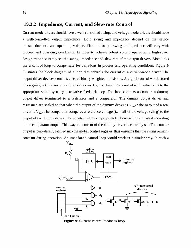
19.3.2 Impedance, Current, and Slew-rate Control
Current-mode drivers should have a well-controlled swing, and voltage-mode drivers should have
a well-controlled output impedance. Both swing and impedance depend on the device
transconductance and operating voltage. Thus the output swing or impedance will vary with
process and operating conditions. In order to achieve robust system operation, a high-speed
design must accurately set the swing, impedance and slew-rate of the output drivers. Most links
use a control loop to compensate for variations in process and operating conditions. Figure 9
illustrates the block diagram of a loop that controls the current of a current-mode driver. The
output driver devices contains a set of binary-weighted transistors. A digital control word, stored
in a register, sets the number of transistors used by the driver. The control word value is set to the
appropriate value by using a negative feedback loop. The loop contains a counter, a dummy
output driver terminated to a resistance and a comparator. The dummy output driver and
resistance are scaled so that when the output of the dummy driver is Vsw/2 the output of a real
driver is Vsw. The comparator compares a reference voltage (i.e. half of the voltage swing) to the
output of the dummy driver. The counter value is appropriately decreased or increased according
to the comparator output. This way the current of the dummy driver is correctly set. The counter
output is periodically latched into the global control register, thus ensuring that the swing remains
constant during operation. An impedance control loop would work in a similar way. In such a
Figure 9: Current-control feedback loop
replicadriverRo
Vsw
Vref=Vsw/2 FSM
U/D
cntrd[N:1]
Load Enable
F w 2xwdf
d0d1
df
d1
d0S0
S1sig
controlregister
N binary sizeddevices
to controlregister

19.3 Transmitters 15
system, a current is injected into a dummy output and an external resistance, and a feedback loop
adjusts the transistor sizes to make the voltage drop (and hence the resistance) of the two branches
the same.6
As mentioned earlier, to reduce both coupling and reflection noise, all drivers need to control the
high-frequency spectral content of their output. This is commonly done by limiting the slew rate
of the driver itself. Variations in process and operating conditions make slew-rate control difficult.
If the desired slew rate is achieved for the slowest possible fabrication and operating conditions,
then the fastest case can exceed the maximum slew rate. On the other hand if the fast case meets
the slew-rate constraint, then the output bandwidth becomes too slow for the desired data rate,
causing ISI in the slow case. Early attempts at slew-rate control tried to find parameters that were
inversely correlated with transistor speed. One method was to divide the driver into multiple
segments, and then turn on each segment sequentially as shown in Figure 10-(a). Commodity
SRAM’s use polysilicon resistors between the driver segments to generate the delay. Thin poly or
gate oxide increases the RC delay and compensates for faster transistor speeds hence decreasing
the variation in output slew rate. More recent methods use an adjustable transition time pre-driver
with explicit feedback as depicted in Figure 10-(b). In one implementation, the speed of the
6. A number of people have proposed to directly measure the transmission line impedance and adjust the drivers to this impedance [9]. In these systems a voltage-mode source-terminated driver is used, and the line is open at the receiver. The feedback loop looks at the voltage on the line before the reflection returns. If the voltage is larger than Vsw/2 the impedance is increased; if it is smaller the impedance of the driver is decreased.
pre-driver
out
δ δ δ
RV
time
out
ctrl
pre-driver
from processindicator (i.e. a VCO)
(a)
(b)Figure 10: Slew-rate control using segmented driver (a), or using controlled pre-driver

16 Chapter 19: High-Speed Signaling
process is measured, and the result of this measurement sets the speed of the predriver [30]. A
more precise implementation uses a controllable delay element as the pre-driver. The control
voltage of the delay elements is generated by a PLL, whose VCO contains identical delay
elements and is locked to the bit-rate clock. In this way, the delay and thus the transition time of
the pre-driver is actively controlled to be a constant fraction of the bit time [53].
The impedance, current, and slew-rate control circuits rely on the ability to measure the I/O
performance indirectly using some dummy circuits. The measurement results adjust controls of
the real circuits to achieve the desired performance. With abundant transistors and reasonable
matching between devices, these techniques work quite well and are commonly used to solve a
number of problems in high-speed link design.
19.3.3 Maximizing Bit Rate
Having described methods for delivering well-shaped bits onto the transmission line, we now
look at what limits the bit rate. The simplest and most commonly used solution to overcome the 6-
8 FO-4 clock cycle limitation is to use a 2:1 multiplexor that drives a new bit on each phase.
Figure 11 shows the effect of bit-time on the pulse width of the multiplexor output signal while
assuming that an aggressive FO-2 buffer chain drives the clock for the 2:1 multiplexor. Although
the multiplexor is fast enough for a bit-time of 2 FO-4’s, the minimum clock period of 8 FO-4 will
limit the system to bit widths of 4 FO-4. Since this performance is fast enough for many
applications (roughly 2Gbps in 0.25-µm process technology), the 2:1 multiplexing architecture is
used in most parallel links [28], [38], and [50]. The latency of these systems is quite modest,
Figure 11: Effect of bit-time on output pulse width of a simple 2:1 multiplexor
Data_O
Data_E
1 2 3 4 50
10
20
30
bit-time (normalized to FO-4)
outp
ut p
ulse
wid
th c
losu
re (
%)clk clk

19.3 Transmitters 17
consisting of about a clock cycle plus the multiplexor and driver latency. Similarly modest is their
power dissipation: CV2f clock power for the parallel to serial converter plus the IV power of the
driver.
Achieving shorter bit time creates a dilemma. To get around the clock limitation requires a large
fanin multiplexor, but the speed of a 4:1 multiplexor limits the bit time to 3-4 FO-4. To create a
faster multiplexor, we need to reduce its output swing and trade gain for increased bandwidth. The
highest possible bandwidth is achieved when the multiplexing occurs directly at the output pin
where both a low time constant (25-50Ω impedance) and small swings are present. Figure 12
shows the basic idea behind this technique. To achieve parallelism through multiplexing,
additional driver legs are connected in parallel. Each driver leg is enabled sequentially by well-
timed pulses of a width equal to a bit-time. Since in this scheme the current pulses at the output
are completely generated by on-chip voltage pulses, the minimum output pulse width is limited
again by the minimum pulse width that can be generated on-chip [32]. An improved scheme,
illustrated in Figure 13-(b) using a grounded-source current-mode output driver, eases that
Figure 12: Higher bandwidth multiplexing at the output pin.
D0 D1 D2
Dout
Dout1
x N
Dout0 Dout2
sel0sel1
sel0 sel1 sel2
Multiplexer
Figure 13: High-bandwidth output-driver implementation using overlapping pulses and grounded source driver. Part (a) shows the overall timing, with the shaded portion markingthe desired bit time. Part (b) shows the circuit diagram of the output driver, but the clock qualification of the data signals is not shown. Part (c) plots the performance of this system
out
outRTERM
RTERM
x 8
data(ck0) data(ck0)
ck3D0 D1 D2
data(ck0)ck1ck2clock(ck3)
Tx-PLL VCO
ck0 ck1 ck2 ck3
Current Pulse
0.6 0.7 0.8 0.9 1.005
10152025 fan-in = 8
bit-width (# FO-4)Am
plitu
de r
educ
tion
(%)
(a) (c)(b)

18 Chapter 19: High-Speed Signaling
limitation [58]. In this configuration, two control signals, both at the slower on-chip clock rate,
are used to generate the output current pulse. In this design, either the transition time of the pre-
driver output or the output bandwidth determine the maximum data rate. Figure 13-(c) illustrates
the amount of pulse time closure with decreasing bit-width for an 8:1 multiplexor utilizing this
technique. The minimum bit-time achievable for a given technology is less than a single FO-4
inverter delay. The cost of this scheme is a more complex clock source, since precise phase-
shifted clocks are required, and an increase in latency (measured in bit-times). In addition, since
the parallel to serial conversion is done at the final buffer stage, this design has larger area and
clock power than a simple 2:1 multiplexor design. The highest speed links use this technique, and
achieve bit-times that are on the order of 1 FO-4.
All of these approaches create transmitters with bit rates that track technology. The rising
frequency of these systems will place increasingly difficult constraints on the design of the
packaging to ensure that coupling, reflection and attenuation does not limit performance.
19.4 ReceiversThe design of the receiver in many ways parallels the design of the transmitter. One of the critical
issues is reducing received noise, which, like the transmitter, requires attention to return currents
and ensuring that the bandwidth of the receiver matches the bit rate. In addition, input
demultiplexing is used to allow these systems to overcome clock and amplifier delay constraints.
Finally, in recent designs closed-loop control is being used to nullify offsets in the input amplifier
or the sample time, and to adjust the bandwidth of the input receiver. Since the performance of the
receiver really depends on the quality of the input signal, we start there.
19.4.1 Input Noise
The main sources of noise for a receiver are mutual coupling between inputs and differences
between chip ground and board ground. Differences between these voltages arise because of the
large image currents that flow through the supply pins to support the output drivers.7 Unless care
is taken, some of this ground noise also appears at the input to the receiver.
7. On-chip bypass capacitance only reduces chip VDD to chip ground noise, and has no effect on the noise between chip ground and board ground.

19.4 Receivers 19
Differential signaling is a good way to minimize the effects of this noise. If both signals are routed
together, ground noise will couple similarly into both signals, changing the common-mode but not
the differential signal. Differential signals also reduce the effect of signal coupling. Since the
signal and its complement are always next to each other, any mutual coupling from one signal is
at least partially compensated by coupling from its complement. As a result, with differential
signaling the required signal amplitude can be quite low, and links can operate successfully with
signals on the order of tens of mV [53].
Conceptually, a transmission line is a differential system, and the same performance can be
achieved in single-ended links. The key is that the signal return path needs to be brought onto the
chip next to the signal, and connected to the reference supply, e.g., chip VDD. With this
connection the difference between chip VDD and board VDD is dropped across the large common
mode inductance of the link, and there is little noise injected between the signal and the on-chip
VDD. This connection makes reference generation easier since the signal is now referenced to the
on-chip supply, but is rarely done in real single-ended link design since it takes as many package
pins as a differential design, and it requires the signal returns to be somewhat isolated from each
other.
In a PCB, the returns will be shorted together on the board and connected to the board VDD
making the ideal connection impossible to achieve. In this case, we need to generate a reference
based on the board VDD. This external reference generation is used in most single-ended link
designs, but has a number of difficulties. It would work well if its coupling to chip VDD and
ground matched the coupling on an input pin. Unfortunately, in nearly all systems, the reference
pin is shared among a large number of inputs, and has a larger capacitance coupling to the chip
supplies than a normal input [28], [38], [50], [45]. This difference in coupling means that a range
of high-frequency on-chip ground noise will couple into the reference line more than the input
pins, causing high-frequency noise to appear at the input of each receiver. The noise manifests
itself in the time domain in the form of reference voltage “spikes.” A high-bandwidth receiver
might sample the input during one of the spikes, causing an error. A receiving amplifier with
limited bandwidth can effectively filter some of this noise, increasing voltage margins. Optimal
noise rejection can be achieved if the amplifier front-end is replaced by an integrator which
averages the polarity of the input signal during the valid-bit time8 [46]. Even with filtering, this
20 Chapter 19: High-Speed Signaling
additional noise coupling means that in real systems single-ended signals need much larger
swings than differential signals to work correctly.
The noise situation is made even worse for simultaneous bidirectional signaling where the system
needs to subtract its transmitted waveform to generate the received waveform. The subtraction is
done by generating a local reference that tracks the value being transmitted. The local reference
needs to match the timing and the voltage of the transmitter. Neither is easy since the transmitted
waveform depends on the effective impedance through the package, which is the least-controlled
section of the transmission line. Mismatches between the reference and the output appear as noise
at the input to the receiver, making this signaling scheme require the largest swings, and benefit
the most from a bandwidth-limited receiver.
19.4.2 Receiver Design
Almost all receivers use at least a two-stage design, where the first stage does the signal
conditioning and usually the sampling function, and the second stage provides the gain and
latching function. To condition the signal, the first stage generally provides the necessary
filtering, translates the input levels from anywhere in the allowable input common-mode range to
a fixed output common-mode voltage, and converts the single-ended input into a differential
signal for the second stage. Since almost all high-speed links use a demultiplexed receiver
architecture, the sampling is done either at the first stage or at the input to the following stage.
Given all these tasks, it is not surprising that high voltage gain is not required, and is often close to
unity.
To get good common-mode noise rejection, the input stage is generally a differential pair
connected to some load devices. The gates of the MOS devices are connected to the input pin and
the reference, or to the differential inputs. The common-mode range sets whether the input pair is
nMOS (inputs near VDD) or pMOS (inputs near ground). Since the stage is being used in a
demultiplexing receiver, one can eliminate all ISI issues introduced by the receiver by shorting the
differential pair outputs before each sample period, thus eliminating any effect of the previous bit.
8. In case the input signal exhibits increased timing uncertainty, the signals near the edge of a bit are very noisy. A “windowed” integrator can be employed to integrate the bit value only around a portion of the bit time when the signal is least likely to change.

19.4 Receivers 21
In most systems the load devices are either resistors or MOS devices operated in their linear
region, so the stage forms a simple differential amplifier. The bandwidth of the amplifier is set by
the RC time constant of the loads.
To build an integrating receiver, the load devices are replaced with switches and capacitors, and
the differential-pair current is integrated over the bit time to see whether the input was mostly
‘one’ or mostly ‘zero’ [46]. Another approach to noise filtering is to change the current in the
differential pair along with the effective resistance of the load device to make the bandwidth of
the amplifier track the bit time. Similar to transmitter slew-rate control, one can leverage the fact
that buffers in the clock generator have been adjusted to have a bandwidth related to the bit rate
[53].
The gain required by the system is provided by the second stage, which is a clocked regenerative
amplifier. This topology has the best speed/power/area trade-off. A common design for this stage
is a StrongARM latch [10]. Given the low gain of the first-stage amplifier and the high offsets of
regenerative amplifiers, the input-referred offset of this topology can be tens of millivolts,
especially if small input devices are used. Again, closed-loop feedback can be used to reduce this
problem. Devices are added that can create an offset in either the first or second amplifier. The
controls to these devices can be set during an initial open-loop calibration step or continuously
adjusted via a feedback loop that averages the received data [21].
Note that in the design of the receiver not much attention is paid to the control the effective
sample point (setup time) of the circuit. Instead the timing-recovery loop uses a receiver in its
feedback to compensate for the setup time. It is critical that for any given process corner the
setup-to-hold window be made as small as possible, since this represents the uncertainty in the
sampling point due to input parameters (edge rate, signal swing, common-mode voltage) for
which the control loop cannot correct.
The latency of the receiver is really the delay through the two-stage receiver plus the
resynchronization delay to realign the data with the system clock of the receiver chip. The delay
of the amplifiers varies, but is roughly one bit time for the first stage, plus 4 FO-4 for the second
stage. The 4 FO-4 delay is roughly the time needed for a regenerative amplifier to take a small-
22 Chapter 19: High-Speed Signaling
swing input to a full-swing out. Power dissipation in the receiver is primarily due to the DC
current of the first-stage amplifier and the clock power for the second stage.
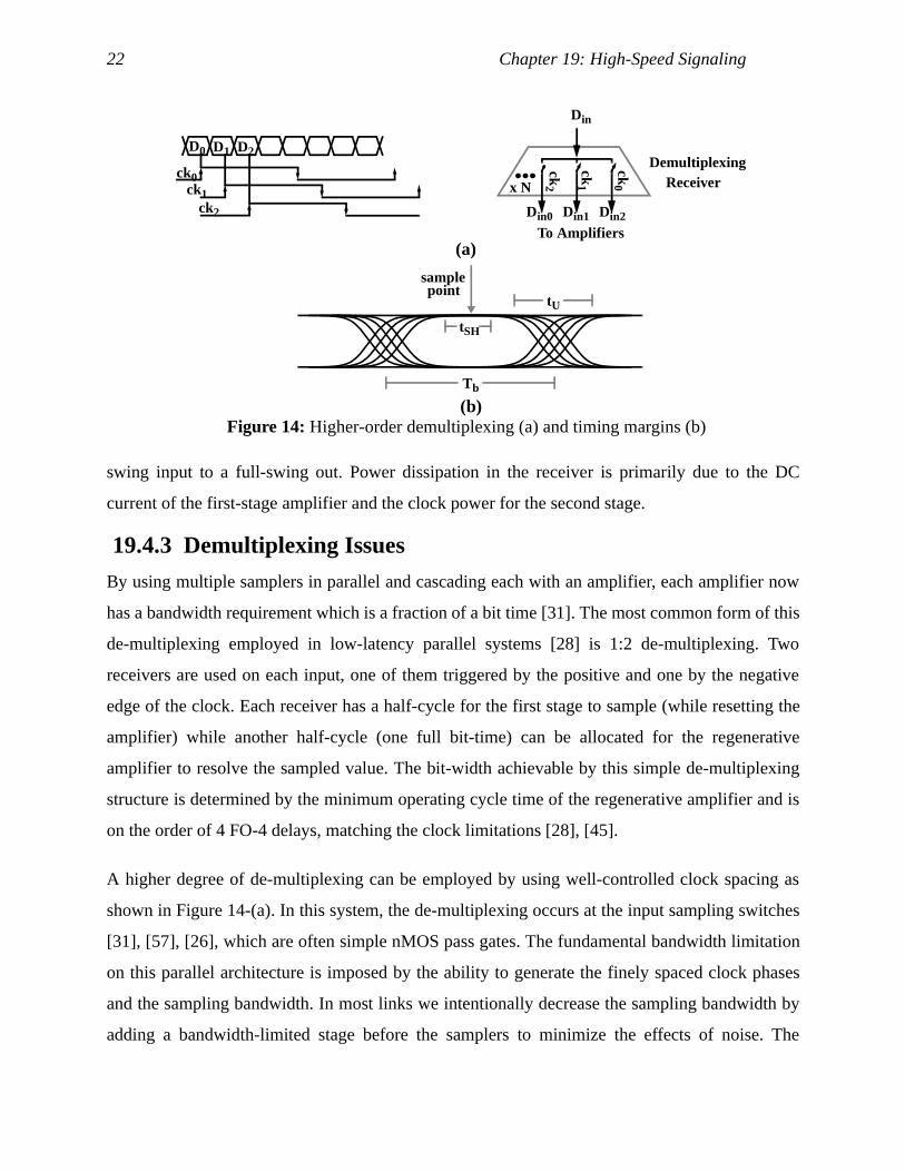
19.4.3 Demultiplexing Issues
By using multiple samplers in parallel and cascading each with an amplifier, each amplifier now
has a bandwidth requirement which is a fraction of a bit time [31]. The most common form of this
de-multiplexing employed in low-latency parallel systems [28] is 1:2 de-multiplexing. Two
receivers are used on each input, one of them triggered by the positive and one by the negative
edge of the clock. Each receiver has a half-cycle for the first stage to sample (while resetting the
amplifier) while another half-cycle (one full bit-time) can be allocated for the regenerative
amplifier to resolve the sampled value. The bit-width achievable by this simple de-multiplexing
structure is determined by the minimum operating cycle time of the regenerative amplifier and is
on the order of 4 FO-4 delays, matching the clock limitations [28], [45].
A higher degree of de-multiplexing can be employed by using well-controlled clock spacing as
shown in Figure 14-(a). In this system, the de-multiplexing occurs at the input sampling switches
[31], [57], [26], which are often simple nMOS pass gates. The fundamental bandwidth limitation
on this parallel architecture is imposed by the ability to generate the finely spaced clock phases
and the sampling bandwidth. In most links we intentionally decrease the sampling bandwidth by
adding a bandwidth-limited stage before the samplers to minimize the effects of noise. The
Figure 14: Higher-order demultiplexing (a) and timing margins (b)
sample point
Tb
tU
tSH
(a)
(b)
ck0ck1
ck2
ck0
ck1
ck2
Din
D0 D1 D2
x N
Demultiplexing
Din1Din0 Din2
Receiver
To Amplifiers

19.5 Clock Generation 23
fundamental limitation of CMOS switches is less than 0.1 FO-4 [24]. Even with simple nMOS
sampler design, the aperture is less than 0.5 FO-4 delays and will not limit the performance of
these links. What does limit the performance of these high-speed links is the quality of the
sampling clocks needed to maintain reasonable timing margins in the link. The precision and
control of these clocks is described in the next section.
19.5 Clock GenerationAlmost all high-speed links use phase-locked loops (PLLs) to generate their internal clocks.
Generating clocks for the transmitter is often easy, since there is no need to precisely align the
phase of the clock(s) to an external reference clock, but generating clocks for the receiver is more
difficult, since the chip must adjust the placement of the clock(s) so that the receiver samples each
bit in the middle of the data eye. Consequently, the receive clocks must track the transmitter
clock’s phase and frequency. There are two independent variables that set the timing relationship
between the transmitter and receiver: one is whether there is a single global frequency source that
is distributed to all the link components, and the other is whether a clock is sent in-phase with the
data. The easiest link designs are the ones where a single clock acts as a frequency source for the
entire system. The disadvantage of this approach is that the global clock is a single point of failure
for the entire system, and if the links are long, one still needs to deliver the clock to all parts in the
system. The alternative is to use separate but nominally equal frequency sources for each end of
the link. In reality, the frequencies in these systems match to a few parts per thousand or better.
The timing-recovery circuit must not only adjust phase but also compensate for the small
frequency difference9.
The two key metrics for judging the quality of the clock generation are phase offset, the DC error
in the placement of the clock; and jitter, the AC component of this error. After exploring basic
PLL operation and the causes of offset and jitter, this section looks at a dual-loop PLL, a
promising architecture that allows a designer to more easily align the receive clock in a wide
variety of system environments.
9. Additional logic must handle the difference in data rate between the two chips.

24 Chapter 19: High-Speed Signaling
19.5.1 PLLs and Phase Noise
Figure 15 shows the two basic approaches to PLLs: VCO-based phase-locked loops (PLLs), and
delay-line-based phase-locked loops or delay-locked loops (DLLs). The basic idea behind the
operation of these two circuits is quite similar: using a control voltage (VC), they both try to drive
the phase of their periodic output signal (clk) to have a fixed relationship with the phase of their
input signal (ref-clk). VCO-based PLLs are more flexible, but are more complicated than those
based on delay lines. Since a VCO changes the phase of its output clock by integrating the
controllable VCO frequency, a VCO-based PLL is inherently a higher order control system which
creates some design challenges [17]. On the other hand, since many applications supply a correct
frequency clock [25], [33], DLLs directly control the output phase by using a Voltage-Controlled
Delay Line (VCDL) which delays its input clock by a controllable time delay to generate the
output clock. The VCDL in this system is simply a delay gain element, resulting in a first-order
(unconditionally stable) control system which is much easier to design.
Both the VCO and VCDL use buffer elements with an additional input that controls their delay.
The feedback loop uses this control to adjust the phase of the outputs. While much effort made to
reduce the effect that VDD or Vsubstrate have on the delay, some sensitivity remains. Thus noise on
these supplies will cause variations in the delay of the buffers and needs to be corrected by the
loop. Unfortunately, like all feedback systems, the control loop has finite bandwidth and can only
Figure 15: PLL and DLL loop topologies(b)
Filter Filter
VCDLVCO
ref clk
clk
PD
ref
clk
PD
(a)
vCvC

19.5 Clock Generation 25
correct for errors below the control bandwidth. High-frequency errors are uncorrected and cause
high frequency phase noise, or jitter, on the output clocks.
In many systems, the jitter from the core PLL is small compared to the jitter caused by the final
clock buffer chain. The final clock buffers are generally CMOS inverters, with no special noise
isolation. For these structures, a 1% change in supply yields roughly a 1% change in delay, which
is more than an order of magnitude larger than the supply sensitivity of a well-designed buffer.
Unless the delay of the core delay line is 10x the clock buffer delay, the clock buffer chain will
dominate the on-chip jitter. For a total buffer delay of about 6 FO-4, and 5% high-frequency
noise, the peak-to-peak jitter of the clock will be around 0.3 FO-4 delays. The jitter for a well-
designed clock with no supply noise, arising from more fundamental noise sources, is roughly
1.5% of the cycle time, or 0.12 FO-4 for a clock cycle of 8 FO-4 delays.
For the high-order multiplexing and de-multiplexing systems described earlier, precisely-spaced
clock phases are used to determine the bit-width. Several techniques can be used to generate these
phases. The simplest is to use a ring oscillator (or a delay line with its input phase locked to its
output phase) and tap the output of each of its stages. For example, a 4-stage oscillator employing
differential stages can generates 8 edges evenly spaced in the 0-360o interval. If the oscillator
operates with a period of 8 FO-4 delay, the phase spacing is 1 FO-4. For even finer phase spacing
than a single buffer delay, phase interpolators can be used to generate a clock edge occurring
halfway between any two output phases [57].
In addition to the high-frequency noise, there are DC errors in the positioning of the clock edges.
These errors arise from mismatches between balanced paths or elements and are a concern in
systems that transmit more than one bit per cycle. To address these matching issues many link
designers use closed-loop control. In a 2:1 multiplexing system where the bit time is a half-cycle,
the bit time is controlled by the time between the rising and falling edges of the clock. To match
the time of each half-cycle, duty-cycle correctors can be added to compensate for small errors
caused by fabrication mismatches [33].
In order to align the clock to the proper position, the timing of the data can be extracted either
from a clock that is bundled with the data or from the transitions in the data signal itself. If the
data signal is used, some coding is necessary to guarantee that enough transitions exist to maintain
26 Chapter 19: High-Speed Signaling
phase lock. Different phase-detector designs can lock the PLL output either directly to the middle
of the bit time, the optimal sample point, or to the data transitions[2]. If the loop locks to the
middle of the data transition region, the true sample clock is generated by shifting the clock phase
by half a bit time.
A common challenge in phase detection for both DLL- and PLL-based timing recovery is that the
circuit has to cancel out the setup time of the input receiver. As discussed in Section 19.4.2, this
usually implies using a receiver replica as the phase detector, resulting in a single binary output,
rather than an analog value of the phase error. Using this phase detector creates a non-linear, or
bang-bang, control system that locks the phase to the middle of the data transitions and causes
difficulties for both VCO and VCDL-based PLLs. For a VCO-based PLL, shifting the clock by
half a bit time is easily done by tapping the appropriate phase from the ring oscillator. However,
VCO-based PLLs are second-order control loops that are hard to stabilize with the binary outputs
of a digital phase detector. Generally these systems will achieve lock only if the initial condition is
very close to the desired final lock point, which means they need a linear phase detector that
initially locks the loop before the non-linear detector is enabled. For VCDL-based designs, bang-
bang control does not cause any difficult issues. However, these designs have their own
limitations when used in links. One is generating a phase shift of half a bit time to center the
sample clock.10 Another is the limited range of the delay line which requires the designer to
ensure that the loop never tries to adjust the phase to a point beyond the range of the delay line. In
addition to added design complexity, for systems where the clock frequencies of the transmitter
and receiver differ slightly, a standard DLL can not be used as it will run out of range.
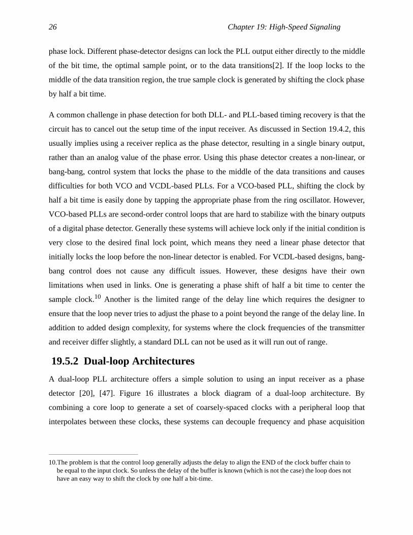
19.5.2 Dual-loop Architectures
A dual-loop PLL architecture offers a simple solution to using an input receiver as a phase
detector [20], [47]. Figure 16 illustrates a block diagram of a dual-loop architecture. By
combining a core loop to generate a set of coarsely-spaced clocks with a peripheral loop that
interpolates between these clocks, these systems can decouple frequency and phase acquisition
10.The problem is that the control loop generally adjusts the delay to align the END of the clock buffer chain to be equal to the input clock. So unless the delay of the buffer is known (which is not the case) the loop does not have an easy way to shift the clock by one half a bit-time.

19.5 Clock Generation 27
and enable the construction of DLLs with infinite phase range. The core loop can be constructed
as a DLL [47] or PLL [20], [29] which can be either analog or digitally-controlled. The peripheral
loop only needs to acquire phase under the control of a digital phase detector and is implemented
as a bang-bang loop with digital control. The separate control of the length of a delay element (the
core loop) and the adjustment of the phase means this architecture can be used to recover clocks
in many different system environments.
Systems with either a single global clock or different local clocks can use a dual-loop architecture.
If a global clock is used, the peripheral loop will select a constant phase shift that compensates for
the internal clock’s buffer delay and the time of flight of the signals. If the local clocks have
slightly different frequencies, this loop will slowly rotate the phase to keep the clock aligned with
the incoming data -- the phase rotation of the peripheral loop compensates for the small frequency
difference in the clocks. This rotation is possible because the peripheral loop does not have any
boundary conditions and can rotate through a full 360 degrees.
To center the sample clock, two matched peripheral loops are connected to a single core loop: one
loop drives the sample clock, and the other drives the clock to the receiver acting as a phase
detector. The clocks are shifted 90o in phase from each other (for a system that transmits 2 bits per
cycle). The peripheral loop feedback sets the phase-detector clock to be in the middle of the
transition region and causes the normal clock to be aligned in the center of the bit eye. The phase
offset of this centering is set by the precision of the 90o phase shift and the matching of the two
clock paths. To eliminate the offset caused by the mismatch in the clock paths, some recent links
Figure 16: Dual-loop PLL/DLL architecture
CORE PLL/DLL
0×θ 1×θ 2×θ 3×θ 4×θ 5×θ
f =x+90oy = x
Phase Selection / InterpolationFilter
Phase Detector
DLL
Samplers
ckref
datain
28 Chapter 19: High-Speed Signaling
use the data receiver directly as the phase detector. These systems periodically send calibration
packets and during this time either the transmit clock or receiver clock is shifted in phase. The
resulting offset can be quite low (< 10ps in a 2-Gbps link) [5].
The dual-loop clocking architecture is an example of how higher levels of integration can be used
to deal with both silicon and system limitations. However, increasing a link’s data rate still
depends on achieving higher on-chip clock rates. As discussed in the following section, basic
technology scaling will assist in the realization of that goal.
19.5.3 Timing Circuit Scaling
Achieving smaller symbol times requires proportional shrinking of both the AC and DC timing
errors. Jitter (which depends on the amount of supply/substrate noise, the sensitivity to noise, and
the bandwidth of the noise tracking) should scale with technology, if certain constraints are met.
Supply/substrate noise is commonly due to digital switching and, hence, is a constant percentage
of the supply voltage. As supply voltage scales with technology, so does the expected noise. The
supply/substrate sensitivity of a buffer is typically a constant percentage of its delay, on the order
of 0.1-0.3%delay/%supply for differential designs using replica feedback biasing [34]. For a
DLL, this implies that the supply- and substrate-induced jitter scales with operating frequency --
the shorter delay in the chain, the smaller the phase noise. This argument also holds for the jitter
caused by the buffer chain that follows the DLL. As technology scales, the delay of the buffer
chain scales, and so does the resulting jitter. For a VCO-based PLL, because noise is integrated by
the VCO, the jitter scaling additionally relies on whether the loop bandwidth (and thus the input
clock frequency) scales. This depends on the system costs of bringing a higher frequency clock
onto the chip.
Scaling of static timing errors is more challenging. The fundamental source of these errors is
random device mismatch, which affects both the position of clock edges and the absolute position
of a receiver’s sampling aperture. For example, mismatch between a timing loop’s phase detector
and the actual receiver becomes an increasing component of static timing offset. Similarly, in
oversampling links with multi-phase clocking, phase spacing errors as a percentage of the bit
width are generally increasing with decreasing transistor feature sizes. The main reason is that the
device threshold voltage is becoming a larger fraction of the clock’s scaled voltage swing.

19.6 Future Trends 29
Fortunately, the static nature of these errors enables their cancellation through static calibration
schemes. For example, the interpolating clock generation architectures described in [57], [35] can
be augmented with digitally controlled phase interpolators [47], and digital control logic to
effectively cancel device induced phase errors. Also, active offset-cancellation circuitry [52] in
comparators will become necessary to mitigate voltage offsets and their effect on timing aperture
position.
Applications of static-timing calibration techniques for very high data rate links will become
more practical as shrinking device dimensions will enable the greater complexity associated with
integrating more support circuits on-chip. Similar circuit complexity can be added to deal with
imperfections of transmitters and receivers. The next section discusses how increasing degrees of
integration can be used to deal with one more obstacle: wire bandwidth.
19.6 Future TrendsThe previous sections have shown that the bit rates of the CMOS interface circuits will continue
to scale with technology, with 2:1 multiplexor interfaces providing 4-5Gbps signaling in 0.1-µm
technology. Unfortunately as bit rates increase, the low-pass filtering of the wire will become
more important, constituting the key obstacle to overcome. The 4-Gbps rate possible today using
high-degree multiplexing is already higher than the bandwidth of copper cables longer than a few
meters.
While designs must account for finite wire bandwidth, it will not fundamentally limit signaling
rate, at least not for a while. The question of how to maximize the number of bits communicated
through a finite bandwidth channel is an old one. It is the basis of modem technology which
transfers 30-50Kbps through the limited bandwidth (4KHz) of phone lines [22], [7], [4]. To
counteract the limited bandwidth, systems make better use of the available signal-to-noise ratio
(SNR) to transmit multiple bits per symbol; see [42] for a good description of these methods. This
section will focus on the issues in applying some of these techniques to systems with very high
symbol rates, where it is difficult to achieve a high-resolution representation of the received
waveform.
30 Chapter 19: High-Speed Signaling
19.6.1 Equalization
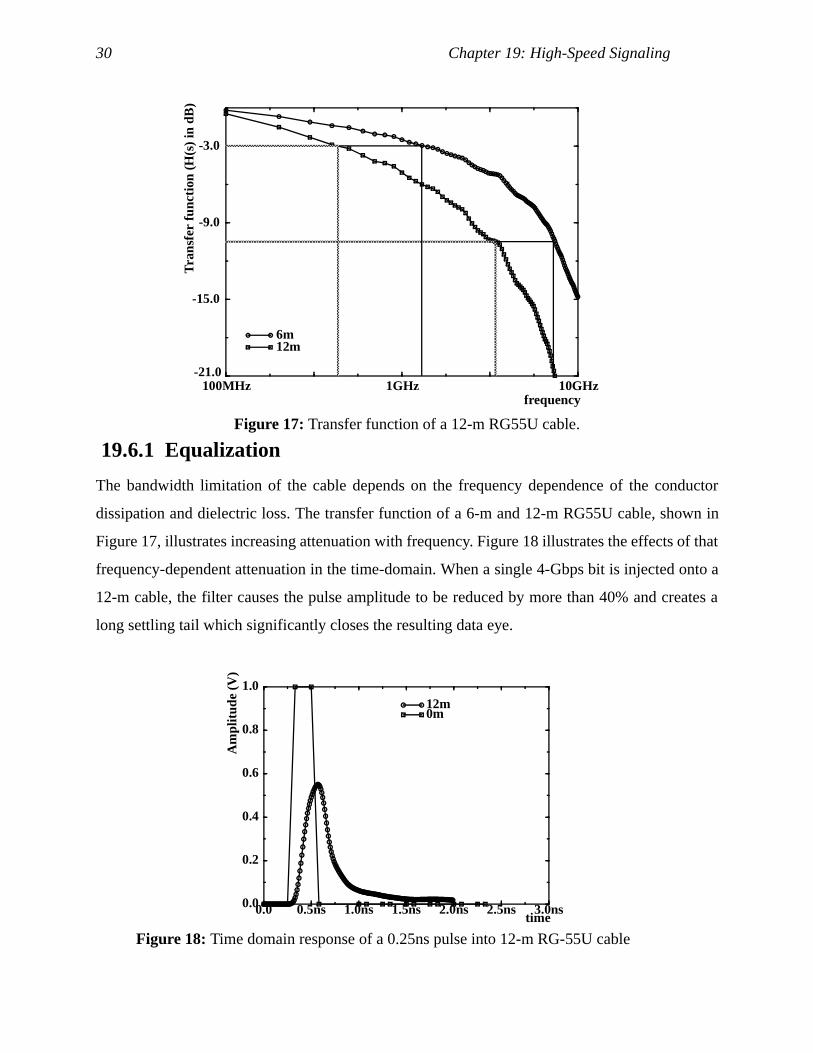
The bandwidth limitation of the cable depends on the frequency dependence of the conductor
dissipation and dielectric loss. The transfer function of a 6-m and 12-m RG55U cable, shown in
Figure 17, illustrates increasing attenuation with frequency. Figure 18 illustrates the effects of that
frequency-dependent attenuation in the time-domain. When a single 4-Gbps bit is injected onto a
12-m cable, the filter causes the pulse amplitude to be reduced by more than 40% and creates a
long settling tail which significantly closes the resulting data eye.
Figure 17: Transfer function of a 12-m RG55U cable.
100MHz 1GHz 10GHz-21.0
-15.0
-9.0
-3.0
6m 12m
frequency
Tran
sfer
func
tion
(H(s
) in
dB
)
Figure 18: Time domain response of a 0.25ns pulse into 12-m RG-55U cable
0.0 0.5ns 1.0ns 1.5ns 2.0ns 2.5ns 3.0ns0.0
0.2
0.4
0.6
0.8
1.012m0m
time
Am
plitu
de (
V)

19.6 Future Trends 31
The simplest way to achieve higher data rate, even with the lossy channels, is to actively
compensate for the uneven transfer function. This can be accomplished either through a
equalizing receiver or a pre-distorting transmitter.
Receiver equalization utilizes a receiver with increased high-frequency gain in order to flatten the
system response [48]. This filtering can be implemented as an amplifier with the appropriate
frequency response. Alternatively the required high-pass filter can be implemented in the digital
domain by feeding the input to an analog-to-digital converter (ADC) and post-processing the
ADC’s output. Using an ADC at the input and building the filters digitally is the usual technique,
since it also allows one to implement more complex non-linear receive filters. While this
approach works well when the data input is bandwidth limited to several MHz, it becomes more
difficult if not impossible with GHz signals because of the required GSamples/sec converters.
Instead of a digital implementation, for these high bit rates, the filter has been implemented as a 1-
tap finite impulse response (FIR) (1-αD) switched-current filter [51].
Most high-speed links use transmitter pre-distortion to equalize the channel [54], [15], [8], [41].
This technique utilizes a filter that precedes the actual line driver. The filter is driven by the bit
stream that is to be transmitted, and the coefficients of the filter are chosen to decrease the low
frequency energy thus equalizing the channel response. In the time domain this reduces the
amplitude of continuous strings of same-value data on the line. The length of the optimal filter
depends on the tail of the single pulse response. It is essentially the number of bits that can affect
the currently transmitted bit. For cable attenuation one or two taps is found to be sufficient [15],
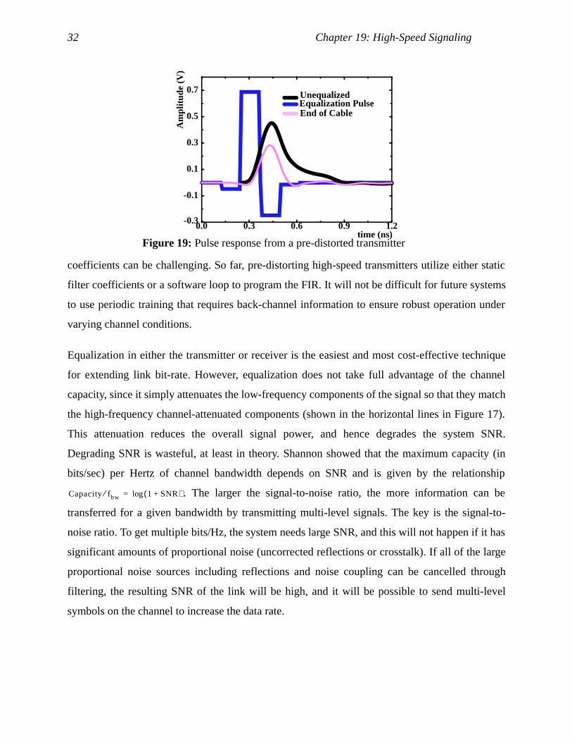
[8], [14]. A sufficiently long filter can compensate even for reflections. The effect of transmitter
equalization is shown in Figure 19. The equalizer transmits small negative pulses before and after
the original pulse to eliminate the tail of the pulse response. The output of this FIR filter is a
quantized representation of the desired output voltage, so the output driver becomes a high-speed
DAC. This DAC already exists in most current-mode output drivers, since it is used to adjust the
output current. The only new requirement is the need for linearity between the control word and
the output current.
The downside of transmitter equalization is that the transmitter does not have any information
about the signal shape at the receiver-end of the channel. Obtaining the appropriate FIR filter
32 Chapter 19: High-Speed Signaling
coefficients can be challenging. So far, pre-distorting high-speed transmitters utilize either static
filter coefficients or a software loop to program the FIR. It will not be difficult for future systems
to use periodic training that requires back-channel information to ensure robust operation under
varying channel conditions.
Equalization in either the transmitter or receiver is the easiest and most cost-effective technique
for extending link bit-rate. However, equalization does not take full advantage of the channel
capacity, since it simply attenuates the low-frequency components of the signal so that they match
the high-frequency channel-attenuated components (shown in the horizontal lines in Figure 17).
This attenuation reduces the overall signal power, and hence degrades the system SNR.
Degrading SNR is wasteful, at least in theory. Shannon showed that the maximum capacity (in
bits/sec) per Hertz of channel bandwidth depends on SNR and is given by the relationship
. The larger the signal-to-noise ratio, the more information can be
transferred for a given bandwidth by transmitting multi-level signals. The key is the signal-to-
noise ratio. To get multiple bits/Hz, the system needs large SNR, and this will not happen if it has
significant amounts of proportional noise (uncorrected reflections or crosstalk). If all of the large
proportional noise sources including reflections and noise coupling can be cancelled through
filtering, the resulting SNR of the link will be high, and it will be possible to send multi-level
symbols on the channel to increase the data rate.
Figure 19: Pulse response from a pre-distorted transmitter
0.0 0.3 0.6 0.9 1.2-0.3
-0.1
0.1
0.3
0.5
0.7 UnequalizedEqualization PulseEnd of Cable
time (ns)
Am
plitu
de (
V)
Capacity fbw⁄ 1 SNR+( )log=

19.6 Future Trends 33
19.6.2 Multi-level Signaling
By transmitting multiple bits in each symbol time, the required bandwidth of the channel for a
given bit rate is decreased. The simplest multi-level transmission scheme is pulse amplitude
modulation. This requires a digital-to-analog converter (DAC) for the transmitter and an analog-
to-digital converter (ADC) for the receiver. During each symbol, N analog levels are transmitted,
communicating log2(N) bits. An example is 4-level pulse amplitude modulation (4-PAM) where
each symbol-time comprises 2-bits of information. A 5-GSym/sec, 2-bit data-eye is shown in
Figure 20 [14]. As was mentioned earlier the key to the operation of these systems is the SNR at
the input receiver. While a 10% reflection noise is not an issue for a binary link (voltage margin
starts at %) it is nearly the entire voltage margin in a 4-PAM system (voltage margin starts at
% of full swing).
For these systems to be successful, all proportional noise sources need to be either small or
accounted for by the link. For systems with good quality channels, multi-level signaling and
equalization might do better than just equalization alone. To really gain the ultimate benefit of
Shannon’s theorem, the system must model and compensate for all sources of proportional noise.
Low-speed links match the analog input waveforms with complex (100-tap) adaptive FIR models
of the channel. For high-speed links the limitations will come from the quality of the ADC and
DAC, and the amount of signal processing power available.
Figure 20: Simulated 4-PAM data-eye
0 100 200 300 400-1.2
-0.8
-0.4
0.0
0.4
0.8
time (psec)
Am
plitu
de (
V)
50±
17±

34 Chapter 19: High-Speed Signaling
19.6.3 DAC and ADCs
The realization of more advanced signaling techniques requires higher analog resolution both for
the transmitter and the receiver. While equalization can be implemented solely with DACs, all the
other techniques require both high-speed DACs and ADCs. The intrinsic noise floor for these
converters is thermal noise, . In a 50Ω environment, the noise is roughly 1-nV/
which is negligible for 2-5 bits resolution even at GHz bandwidth (@ 4 GHz, 3σ <200-µV).
Implementing an output DAC is not foreign to link designers -- DACs are already embedded in
output drivers for impedance or current control. Furthermore, implementing high-speed DACs
with less than 8-bit resolution is less challenging than implementing similar speed and resolution
ADC’s since transmitter device sizes are large and hence inherently less sensitive to device
mismatches due to process variations. Instead, these DACs are limited by circuit issues: primarily
transmit clock jitter, and the settling of output transition induced glitches. Both quantities are
related to the intrinsic technology speed and therefore can be predicted to scale with reduced
transistor feature size. High-speed, low-resolution DACs are rarely used as products; the nearest
comparable product is found in video display RAMDACs achieving 8-bit linearity operating at
320MHz on a 0.8-µm process [49]. In the research domain a 2-bit driver achieving 5-GS/s in a
0.3-µm technology has been demonstrated [14].
The receive-side ADC is more difficult because it requires accurate sampling and amplification of
signals on the order of 30 mV (5 bits of resolution for 1-V signal) at a very high rate. Examples of
high-speed ADC’s can be found in disk-drive read-channels, where a 6-bit flash-ADC operating
at 200MHz has been demonstrated in a 0.6-µm process technology [49]. Recent research
demonstrated a multi-GS/s 4-bit ADC [11] which indicates that high data rate conversion is
possible.
19.7 Conclusion Technology improvements have enabled the development of higher bit-rate links by simply
scaling device speeds. This scaling has been reflected by the fact that bit-rates of links have been
scaling along with the FO-4 technology speed metric. Figure 21 shows the published performance
for both serial and parallel links fabricated in different technologies. Low-latency parallel links
v 4kTR f∆= Hz

19.8 Acknowledgements 35
have maintained bit-times of 3-4 FO-4 inverter delays. Meanwhile, by applying high degrees of
parallelism, the off-chip data rate of serial links has achieved bit-times of 1 FO-4 inverter delays.
Recent research and development results indicate that the fundamental limitation of bit-rate
scaling stems from the communication channel, rather than semiconductor technology and circuit
design. Frequency-dependent channel attenuation limits the bandwidth by introducing inter-
symbol interference. As long as sufficient signal power exists, the simplest technique to extend
the bit-rate beyond the cable bandwidth is transmitter pre-distortion.
Current research is focused on finding methods to extend the performance of links beyond what
can be done with equalization, by exploiting the large SNR of the channel. This interest is leading
to very high-rate ADC and DAC components. While some groups have demonstrated
encouraging results, the practicality of these techniques remains an interesting, but open,
question.
19.8 AcknowledgementsThe authors would like to acknowledge the students in the high-speed links research group at
Stanford University and the technical staff at Rambus for providing valuable data and
suggestions. This work as partially supported by grants from HP, LSI Logic, and DARPA.
Figure 21: Scaling of link bit-time with transistor feature size.
0.0 0.2 0.4 0.6 0.8 1.0 1.2feature size (µm)
0
500
1000
1500
2000
bit-
time
(pse
c)
CMOS low-latCMOS serial

36 Chapter 19: High-Speed Signaling
19.9 References[1] Alvarez, J. et al. “A wide-bandwidth low-voltage PLL for PowerPC microprocessors”
IEEE Journal of Solid-State Circuits, April 1995. vol.30, no.4, p. 383-91
[2] Best, R., “Phase-Locked Loops”, 3rd ed, McGraw Hill, 1997
[3] Black, P.J. et al. “A 1-Gb/s, four-state, sliding block Viterbi decoder” IEEE Journal of
Solid-State Circuits, June 1997. vol.32, no.6, p. 797-805
[4] Boxho, J. et al. “An analog front end for multi-standard power line carrier modem” 1997
IEEE International Solid-State Circuits Conference. Digest of Technical Papers. p. 84-5
[5] Chang, K.Y. et al. “A 2Gb/s Asymmetric Link for High-Bandwidth Packet Switches”, Hot
Interconnects V Symposium Record, August 1997, Stanford, 171-179
[6] Chappell, B. et al., “Fast CMOS ECL receivers with 100-mV worst case sensitivity,”
IEEE Journal of Solid State Circuits, vol. 23, no. 1, pp. 59-67, Feb. 1988
[7] Combe, M. et al. “A second-generation modem analog front-end”, 1992 IEEE
International Solid-State Circuits Conference. Digest of Technical Papers. p. 224-5, 290
[8] Dally, W.J. et al. “Transmitter equalization for 4-Gbps signalling” IEEE Micro, Jan.-Feb.
1997. vol.17, no.1, p. 48-56
[9] DeHon, A. et al. “Automatic impedance control,” 1993 IEEE International Solid-State
Circuits Conference. Digest of Technical, p. 164-5, Feb. 1993.
[10] Donnelly, K.S. et al. “A 660 MB/s interface megacell portable circuit in 0.3µm-0.7µm
CMOS ASIC”, IEEE Journal of Solid-State Circuits, Dec. 1996, vol.31, no.12 p. 1995-
2003
[11] Ellersick, W. et al. “GAD: A 12-GS/s CMOS 4-bit A/D Converter for an Equalized Multi-
Level Link,” Proceedings of 1999 IEEE Symposium on VLSI Circuits. Digest of Technical
Papers, p. 49-52
[12] Esch, G.L., Jr. et al. "Theory and design of CMOS HSTL I/O pads, Hewlett-Packard
Journal Hewlett-Packard, Aug. 1998. vol.49, no.3, p 46-52

19.9 References 37
[13] Farjad-Rad, R. et al. “An Equalization Scheme for 10Gb/s 4-PAM Signalling over Long
Cables” Mixed Signal Conference, July 1997, Cancun, Mexico.
[14] Farjad-Rad, R. et al. "A 0.3-µm CMOS 8-GS/s 4-PAM Serial Link Transceiver",
Proceedings of 1999 IEEE Symposium on VLSI Circuits. Digest of Technical Papers, p.
41-4
[15] Fiedler, A. et al. “A 1.0625 Gbps transceiver with 2x-oversampling and transmit signal
pre-emphasis”, 1997 IEEE International Solids-State Circuits Conference, Digest of
Technical Papers p. 238-9
[16] Galles, M. et al. “Spider: a high-speed network interconnect,” IEEE Micro, J vol.17, no.1,
pp. 34-39, Jan.-Feb. 1997.
[17] Gardner, F.M. “Charge-pump phase-lock loops” IEEE Transactions on Communications,
Nov. 1980. vol.COM-28, no.11, p. 1849-58
[18] Gardner, F. “Phase Lock Techniques”, Wiley 1979
[19] Gray, C. et al. “A Sampling Technique and Its CMOS Implementation with 1Gb/s
Bandwidth and 25-ps Resolution”, IEEE J. of Solid State Circuits, vol. 29, no. 3, ‘94
[20] Horowitz, M. et al. "PLL design for a 500 MB/s interface" 1993 IEEE International
Solids-State Circuits Conference, Digest of Technical Papers, p. 160-1
[21] Hu, T.H. et al. “A monolithic 480 Mb/s parallel AGC/decision/clock-recovery circuit in
1.2-µm CMOS”, IEEE Journal of Solid-State Circuits, Dec. 1993. vol.28, no.12, p. 1314-
20
[22] Ishida, H. et al. “A single-chip V.32 bis modem”, 1994 IEEE International Solid-State
Circuits Conference. Digest of Technical Papers. p. 66-7
[23] International C.C.I.T.T. Recommendations, “V.29-V.33”, Geneva
[24] Johansson, H.O. et al. "Time resolution of NMOS sampling switches used on low-swing
signals" IEEE Journal of Solid-State Circuits, vol.33, no.2, p. 237-45, Feb. 1998.
[25] Johnson, M.G. et al. “A variable delay line PLL for CPU-coprocessor synchronization”
IEEE Journal of Solid-State Circuits, Oct. 1988. vol.23, no.5, p. 1218-23

38 Chapter 19: High-Speed Signaling
[26] Kim, B. et al. “A 30-MHz hybrid analog/digital clock recovery circuit in 2-µm CMOS”
IEEE Journal of Solid-State Circuits, Dec. 1990. vol.25, no.6, p. 1385-94.
[27] Kim, S. et al. “An 800Mbps Multi-Channel CMOS Serial Link with 3x Oversampling,”
IEEE 1995 CICC Proceedings, pp. 451, Feb. 1995.
[28] Kushiyama, N. et al. “A 500-megabyte/s data rate 4.5 M DRAM” IEEE Journal of Solid-
State Circuits, April 1993. vol.28, no.4, p. 490-8
[29] Larsson, P. et al. “A 2-1600 MHz 1.2-2.5 V CMOS clock-recovery PLL with feedback
phase-selection and averaging phase-interpolation for jitter reduction” 1999 IEEE
International Solid-State Circuits Conference, Digest of Technical Papers, p. 356-7, Feb.
1999
[30] Lau, B. et al. “A 2.6GB/s Multi-Purpose Chip to Chip Interface,” 1998 IEEE International
Solid-State Circuits Conference. Digest of Technical Papers, p. 162-3
[31] Lee, K. et al. "A jitter-tolerant 4.5 Gb/s CMOS interconnect for digital display" 1998
IEEE International Solid-State Circuits Conference. Digest of Technical, p. 310-11, Feb.
1998.
[32] Lee K. et al. “A CMOS serial link for fully duplexed data communication”, IEEE Journal
of Solid-State Circuits, April 1995. vol.30, no.4, p. 353-64
[33] Lee, T.H. et al. “A 2.5 V CMOS delay-locked loop for 18 Mbit, 500 megabyte/s DRAM”
IEEE Journal of Solid-State Circuits, Dec. 1994. vol.29, no.12, p. 1491-6
[34] Maneatis, J.G. et al. “Low-jitter process-independent DLL and PLL based on self-biased
techniques” IEEE Journal of Solid-State Circuits, Nov. 1996. vol.31, no.11, p. 1723-32
[35] Maneatis, J.G. et al. “Precise delay generation using coupled oscillators” IEEE Journal of
Solid-State Circuits, Dec. 1993. vol.28, no.12, p. 1273-82
[36] Matick, R. “Transmission lines for digital and communication networks” 3rd ed., IEEE
Press, 1997
[37] McNamara, J. E. Technical Aspects of Data Communication, 2nd ed. Digital Press,
Bedford, MA, 1982.

19.9 References 39
[38] Mooney, R. et al. “A 900 Mb/s bidirectional signalling scheme” IEEE Journal of Solid-
State Circuits, Dec. 1995. vol.30, no.12, p. 1538-43
[39] Moyer, G.C. et al. “The delay vernier pattern generation technique” IEEE Journal of
Solid-State Circuits, April 1997. vol.32, no.4, p. 551-62
[40] Pelgrom, M.J. “Matching Properties of MOS Transistors,” IEEE Journal of Solid State
Circuits, vol. 24, no. 10 pp. 1433, Dec. 1989
[41] Poulton, J. et al. “A Tracking Clock Recovery Receiver for 4Gb/s Signalling”, Hot
Interconnects V Symposium Record, August 1997, Stanford, 157-169
[42] Proakis, J, Salehi M., Communication Systems Engineering, Prentice Hall 1994
[43] Razavi, B. Editor, “Monolithic Phase Locked Loops and Clock Recovery Circuits”, IEEE
Press, 1996.
[44] Reynolds, D. “A 320 MHz CMOS Triple 8 bit DAC with PLL” IEEE Journal of Solid-
State Circuits, Dec. 1994. vol. 29, no.12, pp. 154.
[45] Sidiropoulos, S. et al. “A CMOS 500-Mbps/pin synchronous point to point link interface”
Proceedings of 1994 IEEE Symposium on VLSI Circuits. Digest of Technical Papers p. 43-
4
[46] Sidiropoulos, S. et al. “A 700-Mb/s/pin CMOS signalling interface using current
integrating receivers” IEEE Journal of Solid-State Circuits, May 1997. vol.32, no.5, p.
681-90
[47] Sidiropoulos, S. et al. “A semi-digital DLL with unlimited phase shift capability and 0.08-
400 MHz operating range” 1997 IEEE International Solids-State Circuits Conference,
Digest of Technical Papers, p. 332-3.
[48] Song, B.S. et al. “NRZ timing recovery technique for band limited channels” 1996 IEEE
International Solid-State Circuits Conference. Digest of Technical Papers, p. 194-5.
[49] Spalding, J. et al. “A 200M sample/s 6b flash ADC in 0.6µm CMOS” 1996 IEEE
International Solid-State Circuits Conference. Digest of Technical Papers, p. 320-1.
[50] Takahashi, T. et al. “A CMOS Gate Array with 600 Mb/s Simultaneous Bidirectional I/O
Circuits,” IEEE Journal of Solid State Circuits, vol. 30, no. 12. Dec 1995
40 Chapter 19: High-Speed Signaling
[51] Tamura, H. et al. “Partial response detection technique for driver power reductio in high
speed memory-to-processor communications,” 1997 IEEE International Solid-State
Circuits Conference. Digest of Technical Papers, p. 241-8.
[52] Van de Plassche, R. Integrated Analog-to-Digital and Digital-to-Analog Converters,
Kluwer Academic Publishers, 1994.
[53] Wei, G. et al. "A Variable Frequency Parallel I/O Interface with Adaptive Supply
Regulation", Submitted to ISSCC 2000.
[54] Widmer, A.X. et al. “Single-chip 4*500-MBd CMOS transceiver”, IEEE Journal of Solid-
State Circuits, vol.31, no.12 p. 2004-14, Dec. 1996
[55] Weinlader, D. et al. “An Eight Channel, 36GS/s CMOS Logic Analyzer”, Submitted to
ISSCC 2000.
[56] Wu, J.-T. et al. “A 100-MHz pipelined CMOS comparator” IEEE Journal of Solid-State
Circuits, vol.23, no.6, p. 1379-85
[57] Yang, C.K.K. et al. “A 0.8-µm CMOS 2.5 Gb/s oversampling receiver and transmitter for
serial links”, IEEE Journal of Solid-State Circuits, vol.31, no.12 p. 2015-23
[58] Yang, C.K.K. et al. “A 0.5-µm CMOS 4-Gbps Serial Link Transceiver with Data
Recovery using Oversampling” IEEE Journal of Solid-State Circuits, May 1998. vol.33,
no.5, p. 713-22
[59] Young, I.A. et al. “A PLL clock generator with 5 to 110 MHz lock range for
microprocessors” IEEE Journal of Solid-State Circuits, Nov. 1992. vol.27, no.11, p. 1599-
607
[60] Yukawa, A. et al. “A CMOS 8-bit high speed A/D converter IC”. Proceedings of the Tenth
European Solid-State Circuits Conference p. 193-6