chapter 19 electronic materials. we need some definitions for electrical resistivity and...
TRANSCRIPT
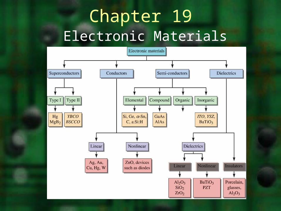
Chapter 19Electronic Materials
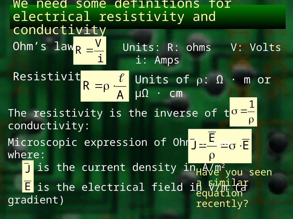
We need some definitions for electrical resistivity and conductivity
Ohm’s law:
Resistivity
i
VR
AR
Units of : Ω · m or µΩ · cm
Units: R: ohms V: Volts i: Amps
The resistivity is the inverse of the conductivity: 1
EE
J
where:
is the current density in A/m2
is the electrical field in V/m (a gradient)E
J
Microscopic expression of Ohm’s law:
Have you seen a similar equation recently?
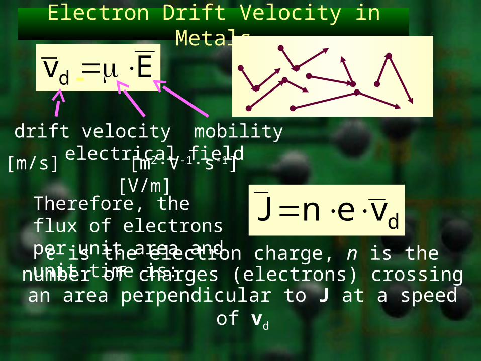
Electron Drift Velocity in Metals
Evd
drift velocity mobility electrical field
[m/s] [m2·V-1·s-1] [V/m]
dvenJ e is the electron charge, n is the number of charges (electrons)
crossing an area perpendicular to J at a speed of vd
- +
Therefore, the flux of electrons per unit area and unit time is:
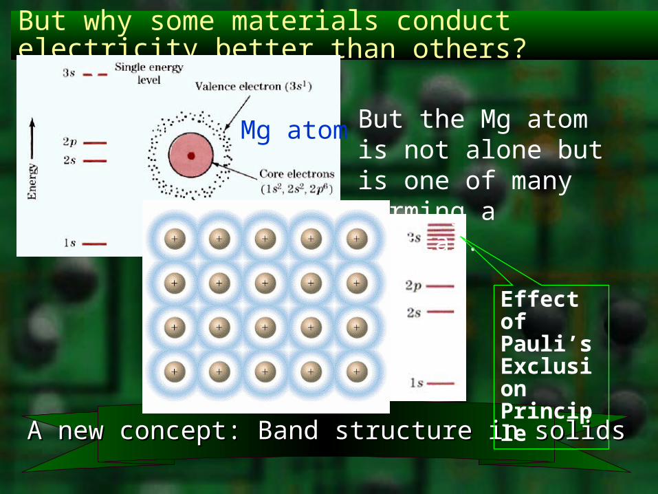
But why some materials conduct electricity better than others?
A new concept: Band structure in solidsA new concept: Band structure in solids
Mg atom But the Mg atom is not alone but is one of many forming a crystal.
Effect of Pauli’s Exclusion Principle
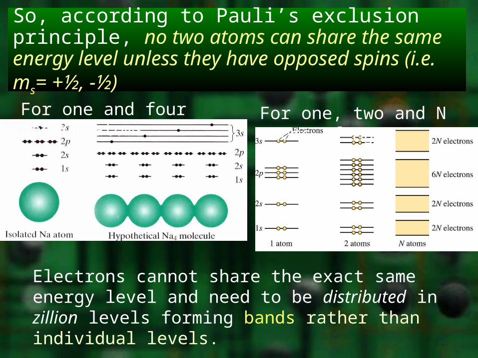
So, according to Pauli’s exclusion principle, no two atoms can share the same energy level unless they have opposed spins (i.e. ms= +½, -½)
For one and four sodium atoms: For one, two and N atoms of Mg:
Electrons cannot share the exact same energy level and need to be distributed in zillion levels forming bands rather than individual levels.
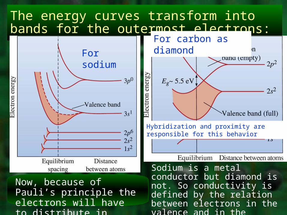
The energy curves transform into bands for the outermost electrons:
For sodium
Now, because of Pauli’s principle the electrons will have to distribute in bands of energy!
For carbon as diamond
Sodium is a metal conductor but diamond is not. So conductivity is defined by the relation between electrons in the valence and in the conduction band
Hybridization and proximity are responsible for this behavior
Then the differences in band energies answer our question about materials with different resistivities.
Note the superposition of both bands:
Reason for the high conductivity of metals
Note the large gap between of
bands
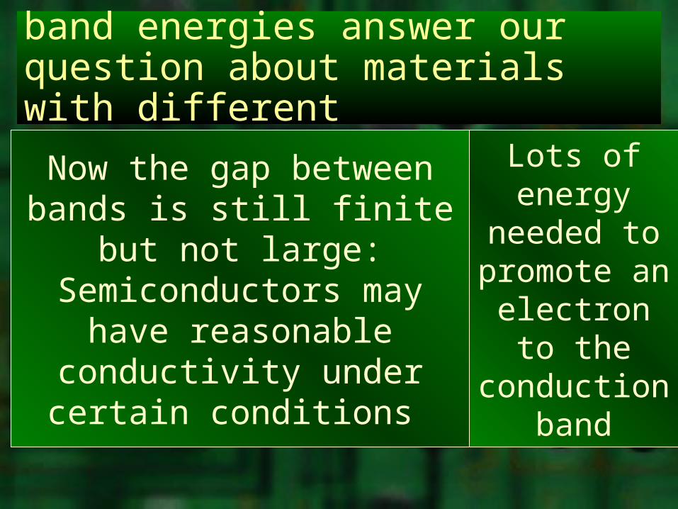
Lots of energy
needed to promote an electron to
the conduction
band
Now the gap between bands is still finite but not large:
Semiconductors may have reasonable conductivity under certain conditions
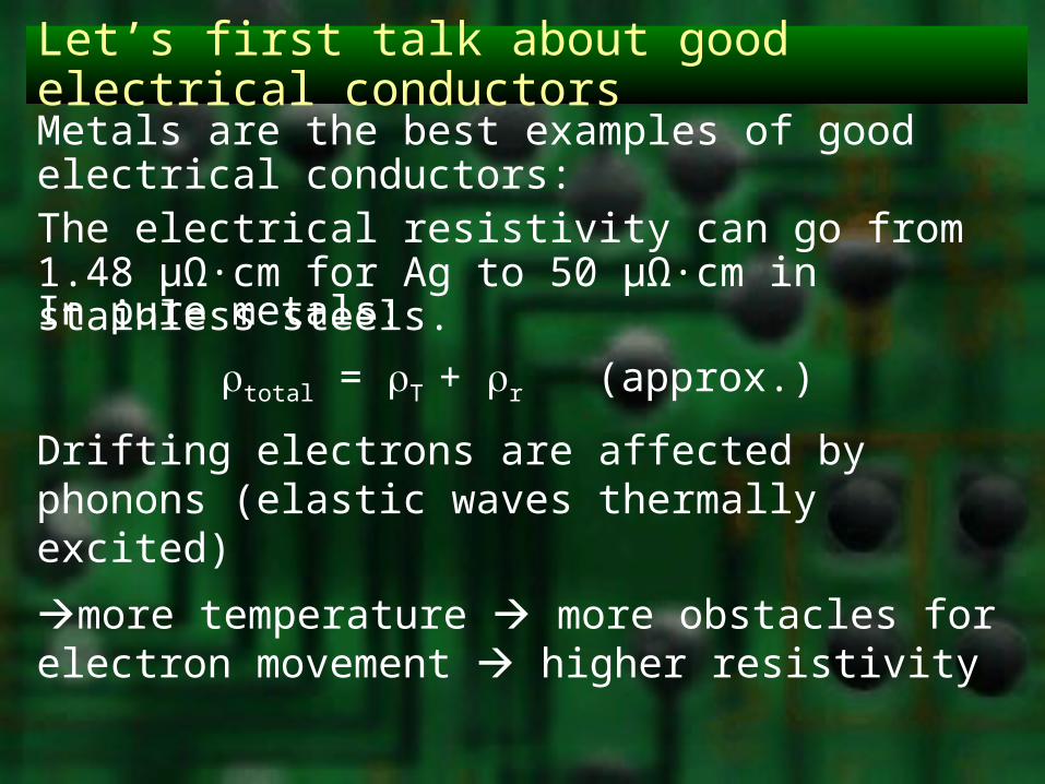
Let’s first talk about good electrical conductorsMetals are the best examples of good electrical conductors:The electrical resistivity can go from 1.48 µΩ·cm for Ag to 50 µΩ·cm in stainless steels.
In pure metals:
total = T + r (approx.)
Drifting electrons are affected by phonons (elastic waves thermally excited)
more temperature more obstacles for electron movement higher resistivity
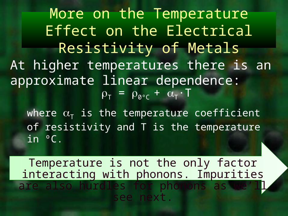
More on the Temperature Effect on the Electrical Resistivity of Metals
T = 0ºC + T·T
where T is the temperature coefficient of
resistivity and T is the temperature in ºC.
At higher temperatures there is an approximate linear dependence:
Temperature is not the only factor interacting with phonons. Impurities are also hurdles for phonons as we’ll see next.
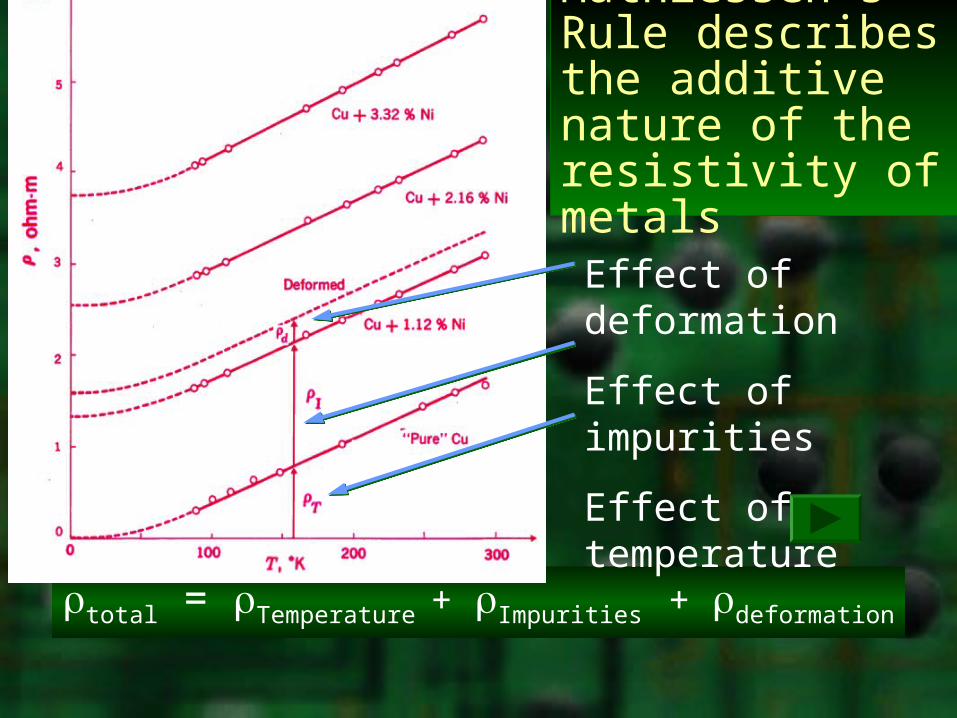
total = Temperature + Impurities + deformation
Mathiessen’s Rule describes the additive nature of the resistivity of metals
Effect of deformation
Effect of impurities
Effect of temperature
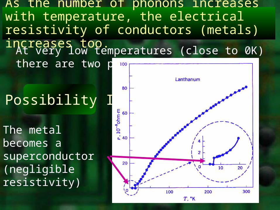
As the number of phonons increases with temperature, the electrical resistivity of conductors (metals) increases too.
At very low temperatures (close to 0K) there are two possibilities
Possibility I
The metal becomes a superconductor (negligible resistivity)
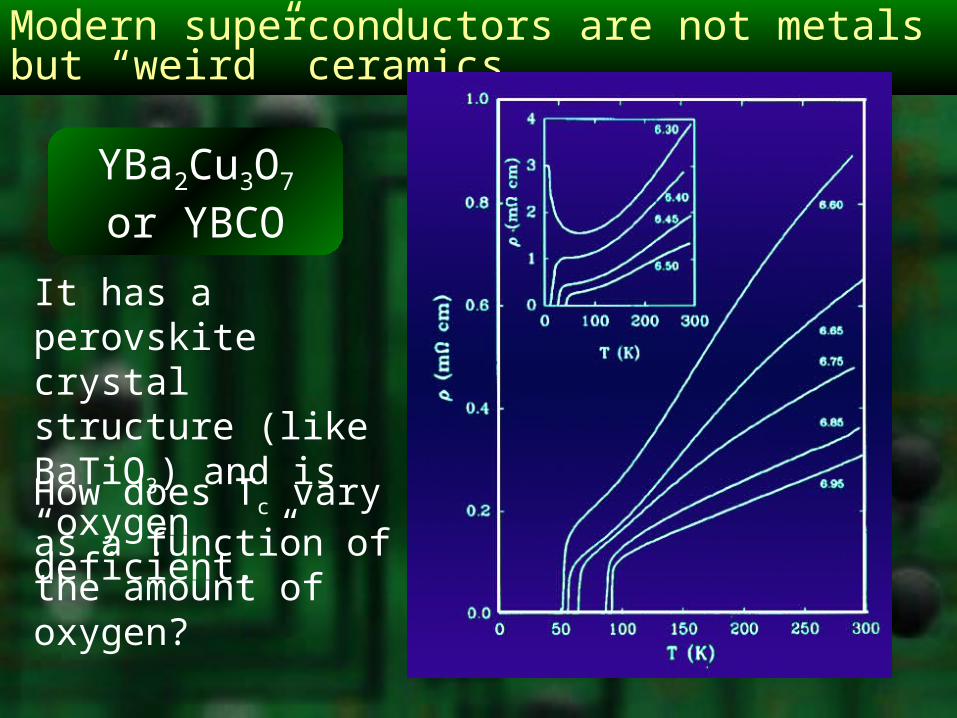
Modern superconductors are not metals but “weird” ceramics
YBa2Cu3O7
or YBCO
How does Tc vary as a function of the amount of oxygen?
It has a perovskite crystal structure (like BaTiO3) and is “oxygen deficient.”
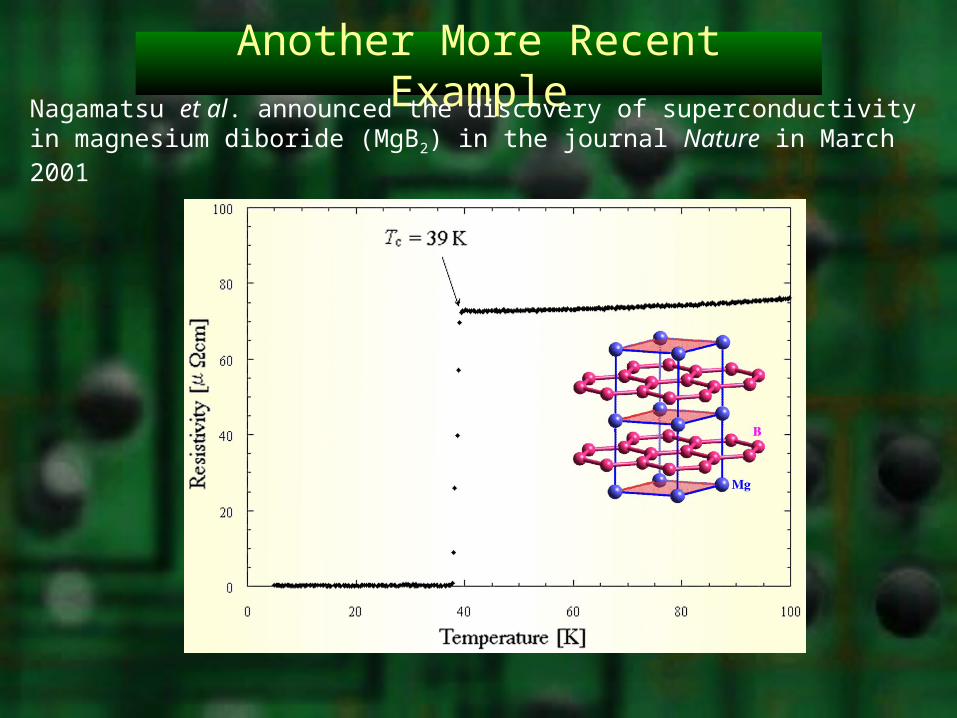
Another More Recent ExampleNagamatsu et al. announced the discovery of superconductivity in magnesium diboride (MgB2) in the journal Nature in March 2001
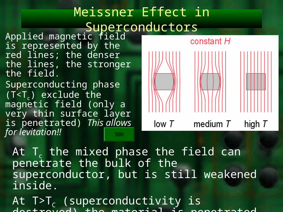
Meissner Effect in SuperconductorsApplied magnetic field is represented by the red lines; the denser the lines, the stronger the field.Superconducting phase (T<Tc) exclude the magnetic field (only a very thin surface layer is penetrated) This allows for levitation!!
At Tc the mixed phase the field can penetrate the bulk of the superconductor, but is still weakened inside. At T>TC (superconductivity is destroyed) the material is penetrated more or less uniformly by the applied magnetic field.
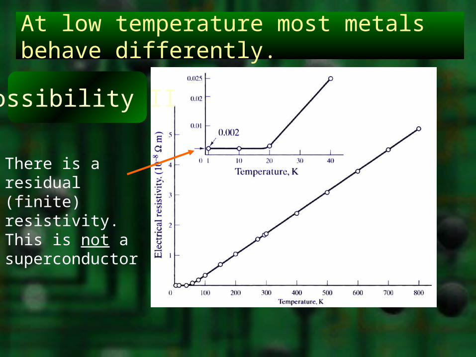
At low temperature most metals behave differently.
Possibility II
There is a residual (finite) resistivity. This is not a superconductor

Let’s introduce the semiconductors• Intermediate behavior between insulators and conductors.
• Their conductivity is highly dependent on temperature and chemical composition
• Two types:
–Intrinsic semiconductors
–Extrinsic semiconductors

Intrinsic semiconductors are those where except for temperature there is no external factor affecting their conductivity.• Elements from Group IV-A (or 14) of the Periodic Table and
some compounds.• Silicon and germanium• What do they have in common?
material Si Ge GaP CdS GaAs
band gap (eV)1.110.672.252.401.42
Intrinsic Semiconductors (cont.)
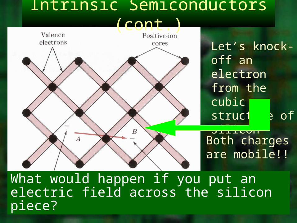
Let’s knock-off an electron from the cubic structure of silicon
Both charges are mobile!!
What would happen if you put an electric field across the silicon piece?
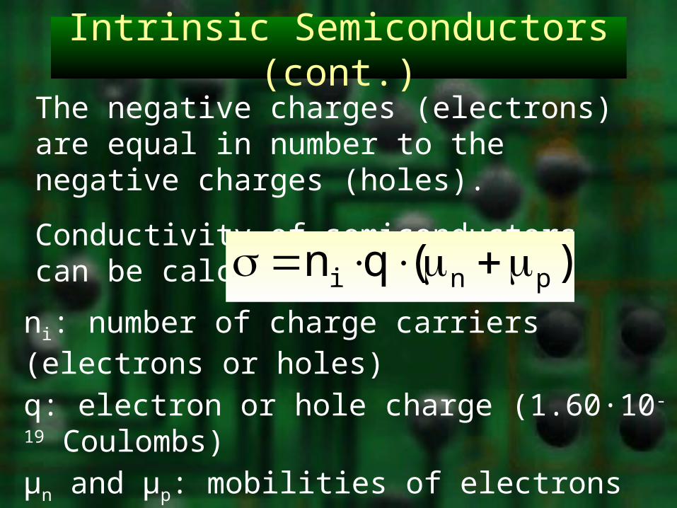
Intrinsic Semiconductors (cont.)
The negative charges (electrons) are equal in number to the negative charges (holes).
Conductivity of semiconductors can be calculated as:
)(qn pni ni: number of charge carriers (electrons or holes)
q: electron or hole charge (1.60·10-19 Coulombs)µn and µp: mobilities of electrons and holes, respectively

Intrinsic Semiconductors (cont.)
Remember that temperature measures internal energy.
Conductivity in semiconductors increases with temperature.
Could you explain why semiconductors behave much different from conductors? Think of the energy gaps.
kT2/Ei
gen
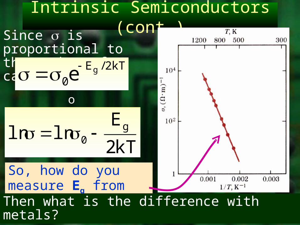
Intrinsic Semiconductors (cont.)Since is proportional to the number of carriers:
kT2/E0
geor
kT2
Elnln g
0
So, how do you measure Eg from the graph?
Then what is the difference with metals?
Extrinsic Semiconductors
Let’s intentionally add impurities with a valence of one higher or one lower, to silicon or germanium.
We need to have an excess of electrons or holes by unbalancing the electronic array of the crystal
Look at the periodic table for candidates!
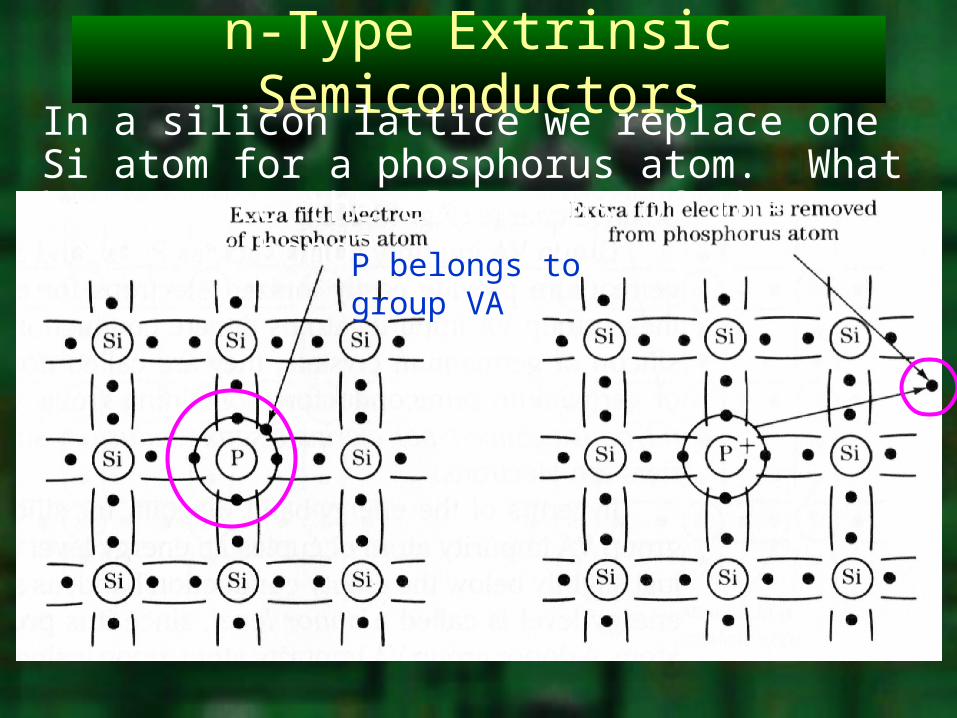
n-Type Extrinsic SemiconductorsIn a silicon lattice we replace one Si atom for a phosphorus atom. What happens to the electrons of the covalent bond?
P belongs to group VA
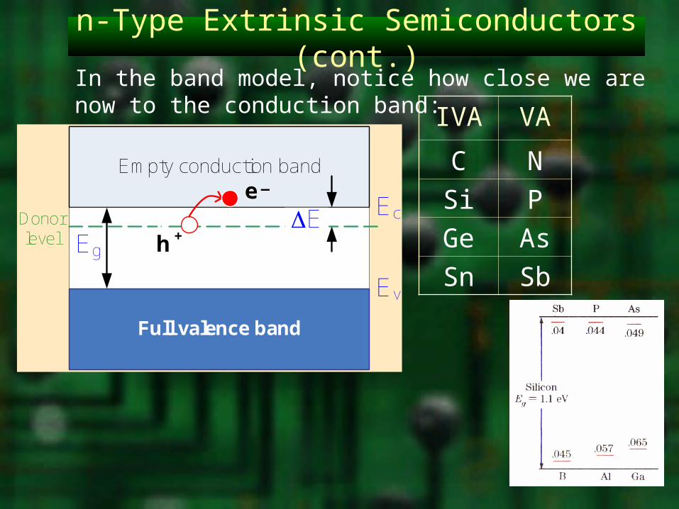
n-Type Extrinsic Semiconductors (cont.)
IVA VA
C N
Si P
Ge As
Sn Sb
In the band model, notice how close we are now to the conduction band:
Empty conduction band
Full valence band
Eg
Ec
Ev
DEh +Donor level h +
e _
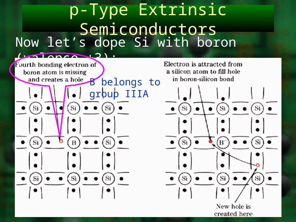
p-Type Extrinsic SemiconductorsNow let’s dope Si with boron (valence +3):
B belongs to group IIIA
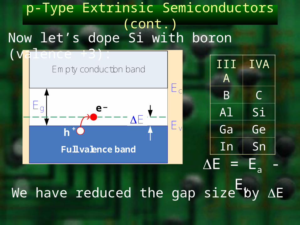
p-Type Extrinsic Semiconductors (cont.)
Empty conduction band
Full valence band
Eg
Ec
EvDE
e _
h +
Now let’s dope Si with boron (valence +3):
We have reduced the gap size by DE
DE = Ea - Ev
IIIA IVA
B C
Al Si
Ga Ge
In Sn
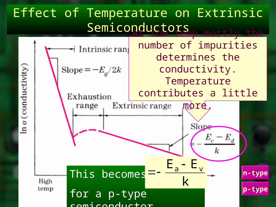
Effect of Temperature on Extrinsic Semiconductors
At low temp mostly the number of impurities
determines the conductivity. Temperature contributes a
little more.
This becomes
for a p-type semiconductor.k
EE va n-type
p-type
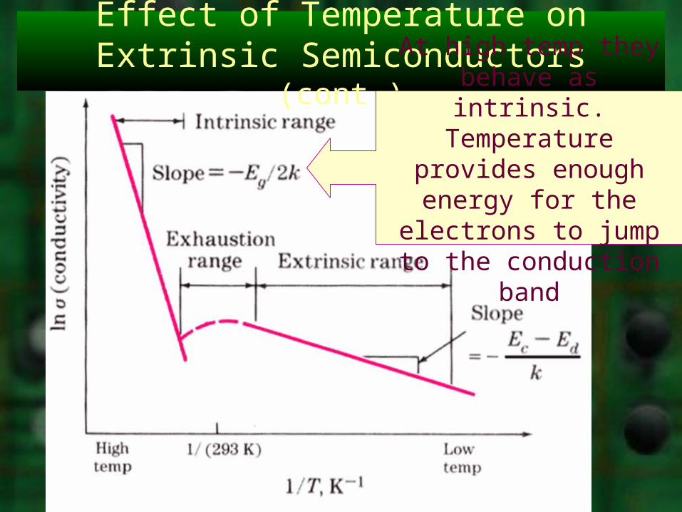
Effect of Temperature on Extrinsic Semiconductors (cont.)
At high temp they behave as intrinsic. Temperature provides enough energy for the electrons to jump to the conduction band
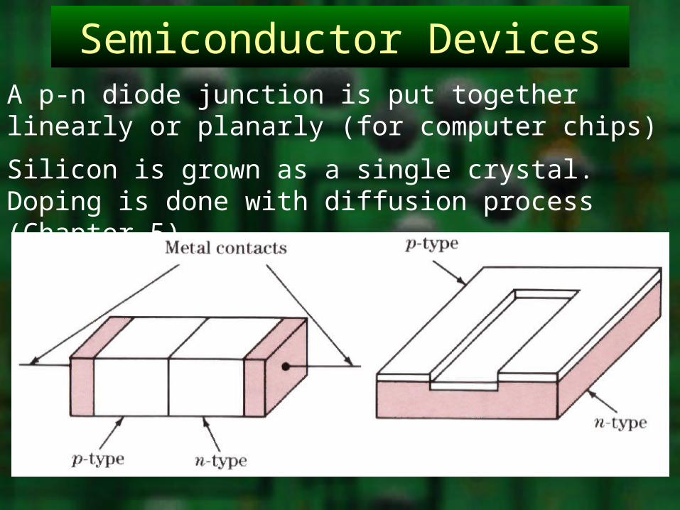
Semiconductor DevicesA p-n diode junction is put together linearly or planarly (for computer chips)
Silicon is grown as a single crystal. Doping is done with diffusion process (Chapter 5).
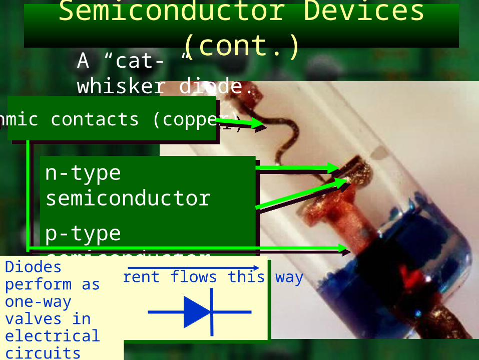
Semiconductor Devices (cont.)A “cat-whisker”diode.
n-type semiconductor
p-type semiconductor
n-type semiconductor
p-type semiconductor
Ohmic contacts (copper)Ohmic contacts (copper)
Current flows this wayDiodes perform as one-way valves in electrical circuits
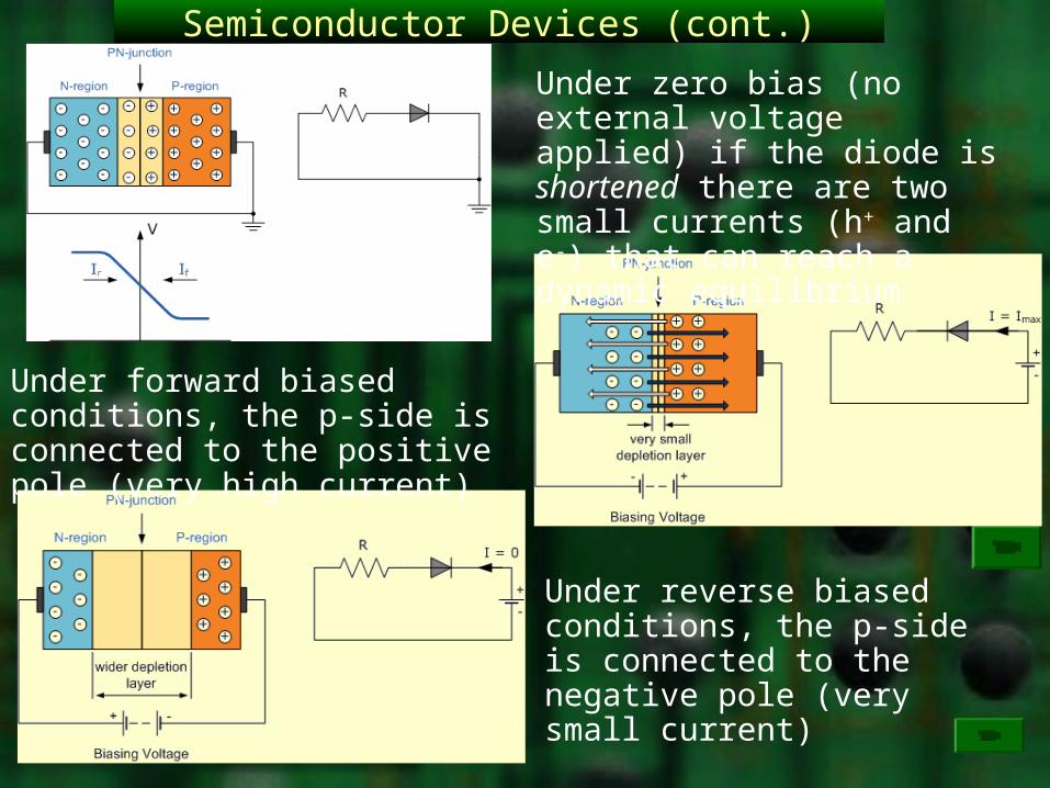
Semiconductor Devices (cont.)
Under reverse biased conditions, the p-side is connected to the negative pole (very small current)
Under zero bias (no external voltage applied) if the diode is shortened there are two small currents (h+ and e-) that can reach a dynamic equilibrium
Under forward biased conditions, the p-side is connected to the positive pole (very high current)
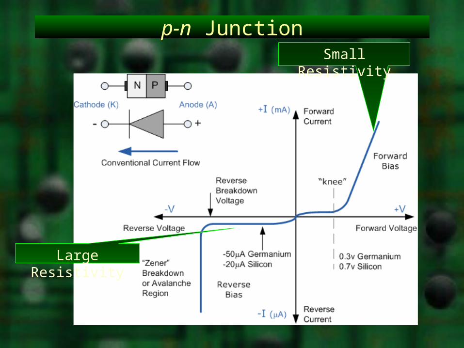
p-n Junction
Large Resistivity
Small Resistivity
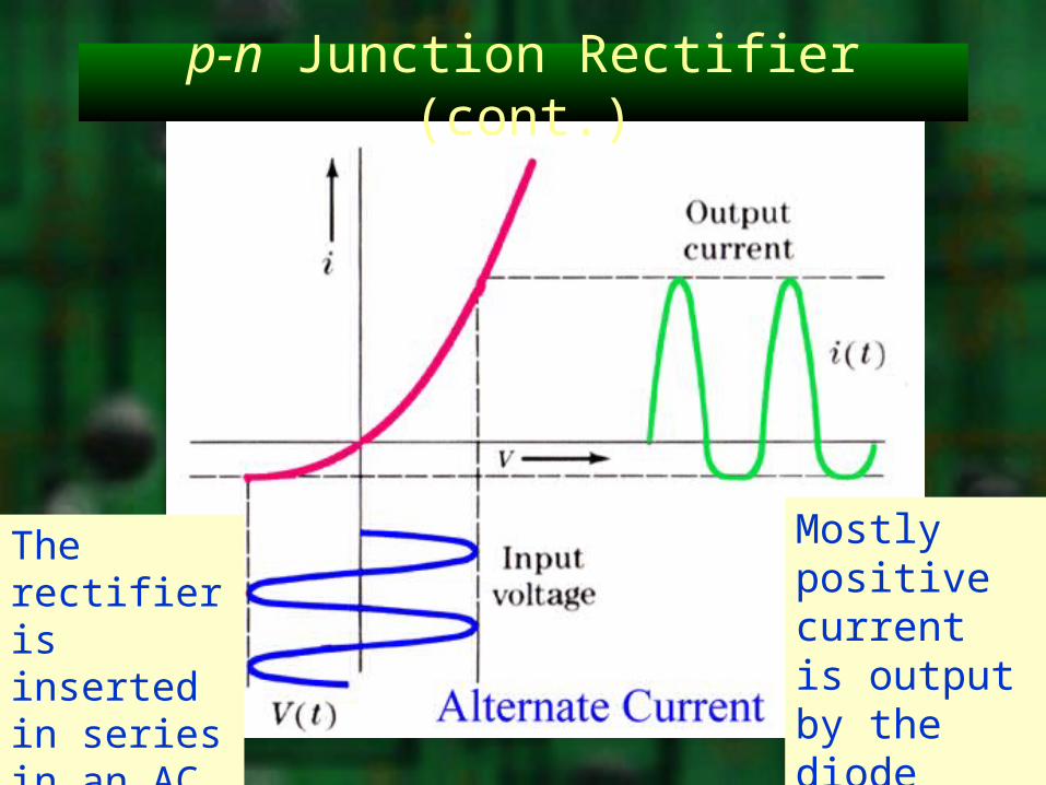
p-n Junction Rectifier (cont.)
The rectifier is inserted in series in an AC circuit
Mostly positive current is output by the diode
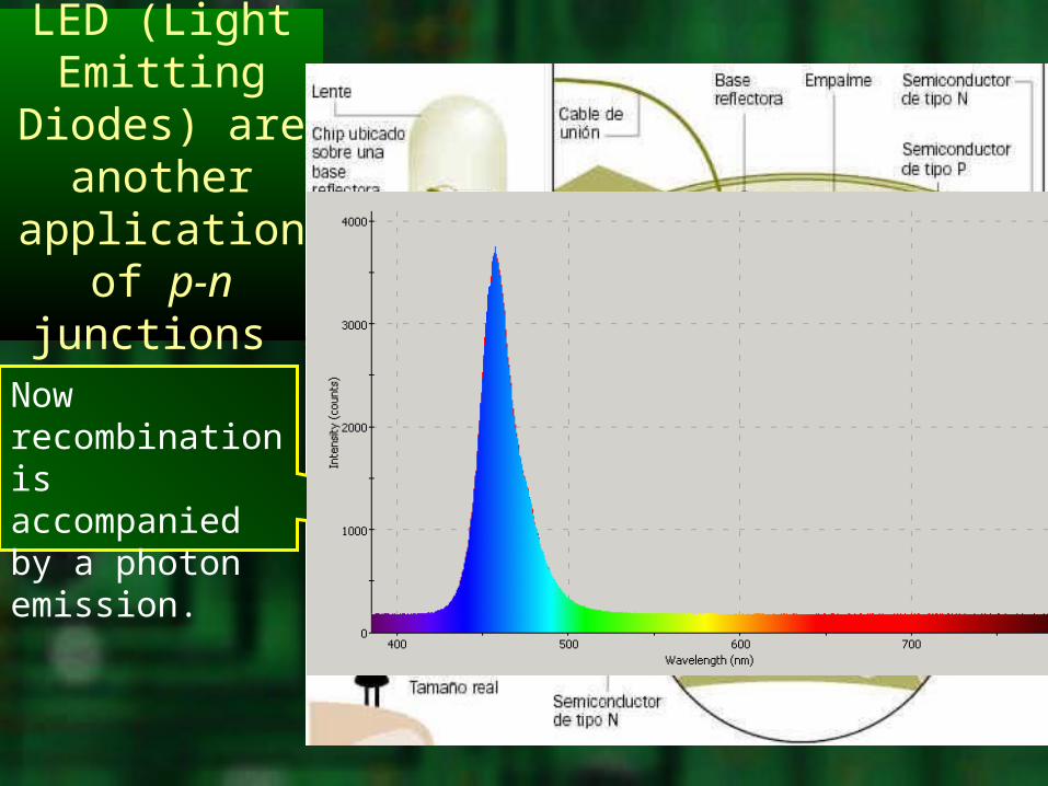
LED (Light Emitting
Diodes) are another
application of p-n junctions
Now recombination is accompanied by a photon emission.
Other Electrical Properties of Materials: Ferroelectricity
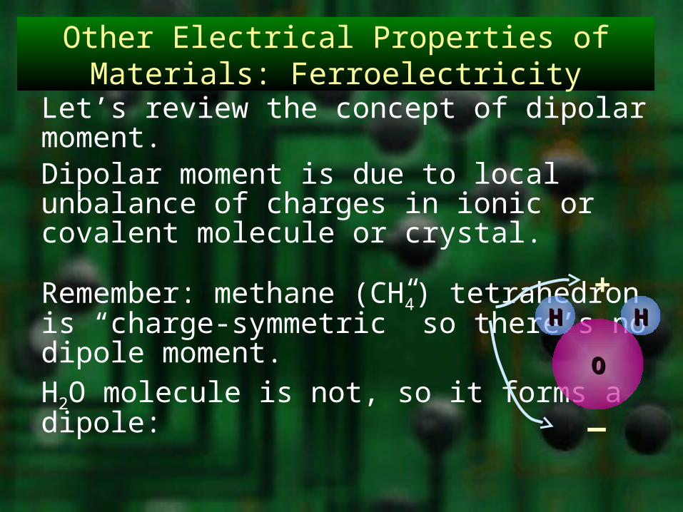
Let’s review the concept of dipolar moment.Dipolar moment is due to local unbalance of charges in ionic or covalent molecule or crystal.
Remember: methane (CH4) tetrahedron is “charge-symmetric” so there’s no dipole moment.H2O molecule is not, so it forms a dipole:
+
OO
HH HH
—
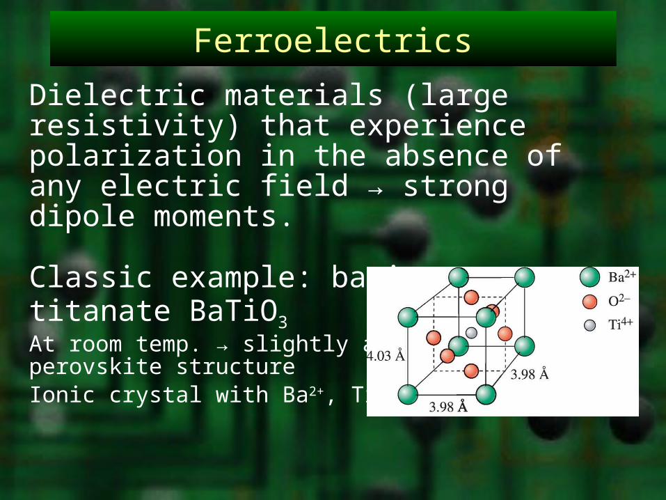
Ferroelectrics
Dielectric materials (large resistivity) that experience polarization in the absence of any electric field → strong dipole moments.
Classic example: barium titanate BaTiO3At room temp. → slightly asymmetric perovskite structureIonic crystal with Ba2+, Ti4+ and O2- ions.
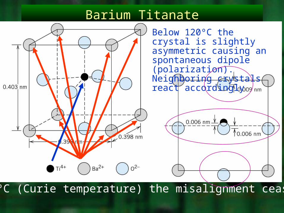
Barium TitanateBelow 120ºC the crystal is slightly asymmetric causing an spontaneous dipole (polarization). Neighboring crystals react accordingly
Above 120ºC (Curie temperature) the misalignment ceases.
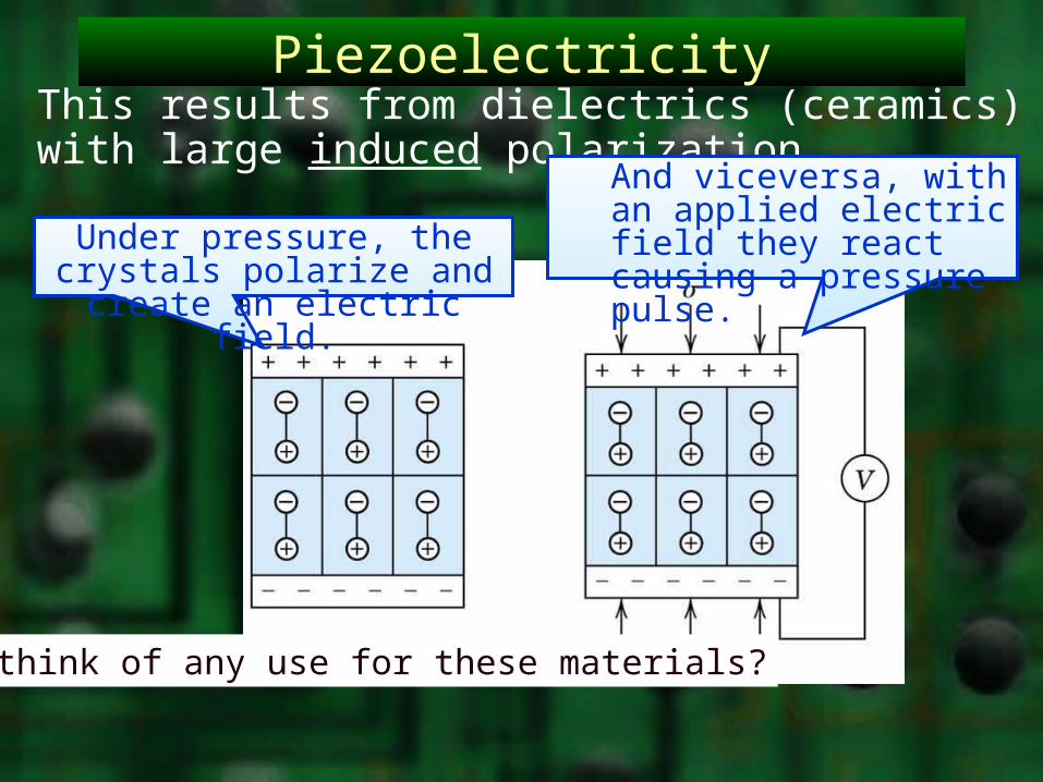
PiezoelectricityThis results from dielectrics (ceramics) with large induced polarization. And viceversa, with an applied
electric field they react causing a pressure pulse.Under pressure, the crystals
polarize and create an electric field.
Can you think of any use for these materials?
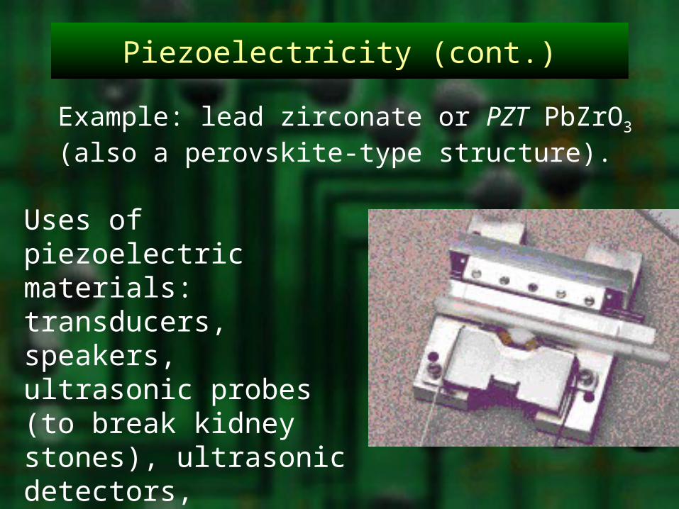
Piezoelectricity (cont.)
Example: lead zirconate or PZT PbZrO3 (also a perovskite-type structure).
Uses of piezoelectric materials: transducers, speakers, ultrasonic probes (to break kidney stones), ultrasonic detectors, actuators, piezoelectric motors, etc.