ceramic capacitor catalogue 2010/11 - … capacitor catalogue 2010/11 holy stone enterprise co.,...
TRANSCRIPT

CERAMIC CAPACITORCATALOGUE 2010/11
Holy StoneEnterprise Co., Ltd.
www.holystone.com.tw www.holystonecaps.com

� Introduction
�The Company Holy Stone EnterpriseCompany Ltd (HolyStone) was establishedin June of 1981 as anagent and distributor ofelectronic components.In 1994, with technology
and cooperation from a Japanese partner, HolyStone began manufacturing multi-layer ceramiccapacitors. Today, Holy Stone is recognized as anindustry leader in application specific ceramiccapacitors.
Holy Stone integrates active and passivecomponent distribution with significantmanufacturing capabilities. Holy Stone’s uniquebusiness model combines the service andinventory management strengths of a broad linedistributor with the technical knowledge and worldclass pricing of a manufacturer.
Holy Stone was founded by five engineers in 1981.Since this point, Holy Stone has maintained afocus and commitment to providing customerswith innovative products and exceptional service.The result of that unwavering commitment isevident in Holy Stone’s phenomenal growth (2009revenues of US$412 million). Holy Stone alsomaintains a high profile on the Taiwan StockExchange, ranked in the top 100 companies andthe leader among its peers.
�Manufacturing FacilitiesHoly Stone capacitorsAre produced in a modern40,000 square meterfactory located in Lungtan,Taiwan. In addition to theLungtan factory, Holy Stonehas facilities in Dongguan and Wujiang China.The advanced materials research laboratory islocated in Japan. The factory operating systemsare certified to ISO-9001and ISO-14001.
�Sales and Support LocationsHoly Stone administrativeheadquarters are locatedin Taipei, Taiwan.Holy Stone maintainssales and support officesin Kaohsiung Taiwan,Dongguan China andShanghai China.
Holy Stone Enterprise Company Ltd hassubsidiary companies in North America and inEurope. Holy Stone International, located inMurrieta, California, U.S.A. is responsible forsales and technical support in the Americas. HolyStone (Europe) Ltd, located in Norwich, Englandis responsible for sales and technical service forEurope. Holy Stone opened its Singapore office toservice southeast Asia. Holy Stone also has anetwork of independent representatives,distributors and agents throughout the world.
�The EnvironmentHoly Stone is committed to achieving andmaintaining a healthy environment. Holy Stone isalso among the first suppliers of halogen freeepoxy coated capacitors. The factory is Certifiedto ISO-14001 and all standard products aredesigned and produced conforming to full RoHScompliance.
�Our EmployeesHoly Stone’s success is measured by thesatisfaction of our customers and share holders.Achieving that satisfaction is the result of the sumcontribution of our employees. Thosecontributions come from all of our employees,whether they are engaged in administrativefunctions, manufacturing our goods or servicingour customers. Holy Stone strives to maintain awork environment that stimulates creativity,encourages enthusiasm and rewards results.

- 1 -
Component Quick Reference ------------------------------------------ 2
Capacitor Availability Guide --------------------------------------------- 3-4
Products Series ----------------------------------------------------------- 5-34
Technical Specifications -------------------------------------------------- 35-41
Packing Information ------------------------------------------------------ 42-44
EIA Designations ------------------------------------------------------------ 45
Precautionary Information ---------------------------------------------- 46-49
Reducing Short Circuit Risks –Super Term ----------------------- 50-51
Coated Products for Surface Arc Prevention --------------------- 52-53
ROHS Compliant ----------------------------------------------------------- 54
ISO Certifications ---------------------------------------------------------- 55
CONTENTS
Contents

Component Quick Reference
- 2 -
Product Series Application PageHVC series --High Voltage Capacitors
For Power Circuits(Backlight Inverter, DC to DC,…) 5-8
SCC series --Safety Capacitors
For Isolation and Protection Circuits (UL,EN132400 Class X2/Y3,X1/Y2) 9-11
TCX series --Trigger Capacitors For DSC Strobe Circuits 12-13
LDC series --Low Distortion Capacitors For Oscillation and Filter Circuits 14-15
NCC series --Normal Chip Capacitors For Decoupling Circuits 16-17
HCC series --High Capacitance MLCC-More than 1uF For Smoothing (DC to DC) and Decoupling Circuits 18-19
HCN series --High Capacitance NP0
For ADSL/XDSL (Replacement for Film Capacitor) 20-21
HCX series --High Capacitance X7R For Input, Output Filters (DC to DC) 22-23
SAC series --Tip & Ring Capacitors For telephone line ringer circuits 24-25
HBC series --Low-Loss High Frequency Snubber Capacitors
For High Frequency Lighting Ballasts 26-27
HTC series --X8R rated to +150°C For high temperature applications 28-29
LCC series --Large Size MLCC Capacitors 1515 to 7565
For Voltage Multipliers, Power circuit (DC-DC, Ballast, Snubber), Surge protection, Industrial control, … 30-31
SMC series --Stacked MLCC Capacitors
For Power Circuits(Backlight Inverter, DC to DC, Surge protection …) 32-34

Capacitance Availability Guide – Standard MLCC
- 3 -
Vdc 0201 0402 0603 0805 1206 1210 1808 1812 1825 2220 2225
6.3vNP0
X7R 2.2uF 4.7uFX5R 100nF 1uF 10uF 22uF 47uF 100uF
10VNP0
X7R 100nF 2.2F 4.7uF 10uF 10uFX5R 1uF 4.7uF 10uF 22uF 22uF
16VNP0 3.3nF 10nF 27nF 47nF 120nFX7R 100nF 2.2uF 2.2uF 4.7uF 22uFX5R 100nF 2.2uF 10uF 22uF 22uF
25VNP0 3.3nF 10nF 10nF 22nF 47nFX7R 10nF 1uF 1uF 2.2uF 10uFX5R 100nF 1uF 4.7uF 10uF 10uF
35VNP0
X7R 470nF 1uF 4.7uF 2.2uF 10uFX5R 1uF 10uF
50VNP0 470pF 3.3nF 10nF 10nF 22nF 47nF 82nFX7R 10nF 100nF 330nF 1uF 2.2uF 4.7uF 4.7uF 10uF 6.8uFX5R 1uF
100V
NP0 270pF 1.2nF 6.8nF 10nF 18nF 56nF 56nF 68nFX7R 18nF 100nF 470nF 2.2uF 2.2uF 2.2uF 4.7uF 4.7uF
X5R
200VNP0 270pF 1.2nF 5.6nF 8.2nF 12nF 47nF 47nF 56nFX7R 47nF 100nF 470nF 1uF 1.5uF 2.2uF 2.2uFX5R
250VNP0 270pF 1.2nF 5.6nF 8.2nF 12nF 47nF 47nF 56nFX7R 47nF 100nF 470nF 1uF 1.5uF 2.2uF 2.2uFX5R
500VNP0 680pF 2.2nF 3.9nF 1.8nF 8.2nF 39nF 39nF 47nFX7R 22nF 56nF 100nF 39nF 220nF 270nF 470nF 470nFX5R
630VNP0 2.2nF 3.9nF 1.8nF 8.2nF 27nF 27nF 33nFX7R 33nFX5R
1KVNP0 1nF 1nF 1.2nF 6.8nF 12nF 12nF 15nFX7R 1nF 10nF 27nF 15nF 47nF 100nF 100nF 100nFX5R
2KVNP0 390pF 680pF 1.2nFX7R 1.5nF 2.7nF 3.3nF 10nF 18nF 18nF 18nFX5R
3KVNP0 39pF 1nF 1.2nF 1.2nFX7R 1.8nF 2.7nFX5R
4KVNP0
X7R 1nFX5R
5KVNP0 27pF 150pFX7R
X5R
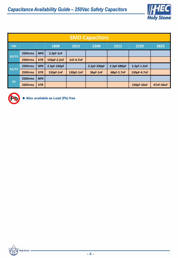
Capacitance Availability Guide – 250Vac Safety Capacitors
- 4 -
SMD CapacitorsVdc 1808 1812 2208 2211 2220 2825
X2/Y3250Vrms NP0 2.2pF-1nF
250Vrms X7R 150pF-2.2nF 1nF-4.7nF
X1/Y2250Vrms NP0 2.2pF-150pF 2.2pF-330pF 2.2pF-680pF 2.2pF-1.2nF
250Vrms X7R 150pF-1nF 130pF-1nF 36pF-1nF 68pF-2.7nF 130pF-4.7nF
X2250Vrms NP0
250Vrms X7R 150pF-10nF 47nF-56nF
� Also available as Lead (Pb) free
� How To Order
HVC Series High Voltage NP0 and X7R Capacitors Up to 5KV
Operating Temperature -55~+125 ԨRated Voltage 100Vdc to 5000Vdc
Temperature CoefficientNP0 : d ± 30ppm/ Ԩ , -55~+125 Ԩ (EIA Class ǿ )X7R : d ± 15% , -55~+125 Ԩ (EIA Class Τ )
Dissipation Factor NP0: Q1000ؤ ; X7R : D.F.2.5أ%Insulation Resistance 10Gȍ or 500/C ȍ� whichever is smallerAgeing NP0:0% ; X7R: Typically 1.0% per decade of time
Dielectric Strength100V أ V ᧸ 500V : 200% Rated Voltage500V أ V ᧸ 1000V : 150% Rated Voltage1000Vأ V : 120% Rated Voltage
� Summary of Specifications
� Special internal electrode design offerthe highest voltage rating.
� Surface mount suited for solder wave andreflow soldering.
� High reliability.� RoHS compliant.
� Suitable for LAN/WLAN interface,Back-Lighting Inverter, DC-DC Converters,Ballast, Modems & Power Supplies.
Product Code
C : MLCCMultilayerCeramic Capacitor
Chip Size
EX. :0603 0805 12061210 1808 18122220 2225
Dielectric
Ex. :N : NP0X : X7R
CapacitanceUnit : pFEx. :2R0 : 2.0pF100 : 10×100
471 : 47×101
102 : 10×102
Tolerance
Ex. :C : +/-0.25pFD : +/-0.50pFJ : +/- 5%K : +/-10%M : +/-20%
Rated Voltage Ex. :101 : 100Vdc251 : 250Vdc501 : 500Vdc631 : 630Vdc102 : 1000Vdc202 : 2000Vdc302 : 3000Vdc402 : 4000Vdc502 : 5000Vdc
Packaging
T : Tape& Reel
B : Bulk
SpecialRequirement Ex. :O : Arc
PreventionCoating
X : PolymerTermination (Super Term)
HVC Series - High Voltage Capacitors
Holy Stone high voltage products are designed and manufactured to meet the general requirements ofinternational standards. This product offering is well suited for commercial and industrial applications andincludes NP0 (C0G) and X7R characteristics in sizes 0603 to 2225 and with working voltages up to 5KV.
� Applications.� Features
C 1210 X 103 K 102 T X
- 5 -

W
T
BW B
L
� Dimensions
� Capacitance Range – NP0 100Vdc to 1KVdc
TYPE L W T (max) B (min) BW (min)
0603 1.60±0.1[.063±.004]
0.80±0.1[.031 ±.004]
0.90[.039]
0.40[.016]
0.15[.006]
0805 2.00±0.20[.079±.008]
1.25±0.20[.049±.008]
1.45[.057]
0.70[.028]
0.20[.008]
1206 3.20±0.30[.126±.012]
1.60±0.20[.063±.008]
1.80[.071]
1.50[.059]
0.30[.012]
1210 3.20±0.30[.126±.012]
2.50±0.20[.098±.008]
2.60[.102]
1.60[.063]
0.30[.012]
1808 4.60±0.30[.181±.012]
2.00±0.20[.079±.008]
2.20[.087]
2.50[.098]
0.30[.012]
1812 4.60±0.30[.181±.012]
3.20±0.30[.126±.012]
3.00[.118]
2.50[.098]
0.30[.012]
1825 4.6±0.30[.181±.012]
6.35±0.40[.250±.016]
3.00 [.118]
2.50[.098]
0.30[.012]
2220 5.7±0.40[.220±.016]
5.00±0.40[.197±.016]
3.00 [.118]
3.50 [.137]
0.30[.012]
2225 5.7±0.40[.220±.016]
6.35±0.40[.250±.016]
3.00 [.118]
3.50 [.137]
0.30[.012]
Unit : mm [inches]
HVC Series - High Voltage Capacitors
- 6 -
Consult HEC for thickness information
2R0
3R3
3R9
5R0
8R2
100
120
150
180
220
270
330
390
470
560
680
820
101
121
151
181
221
271
331
391
471
561
681
821
102
122
152
182
222
272
332
392
472
562
682
822
103
123
153
183
223
273
333
393
473
563
683
B B B B B B B B B B B B B BB B B B B B B B B B B B B B B B B B B B B B BB B B B B B B B B B B B B B B B B B B B B B BB B B B B B B B B B B B B B B B B B B B B B BB B B B B B B B B B B B B B B B B B B B B B B B B B B C C C DB B B B B B B B B B B B B B B B B B B B B B B B B B B C C C DB B B B B B B B B B B B B B B B B B B B B B B B B B B C C C DC C C C C C C C C C C C C C C C C C C C C C C C C C C C
B/C B/C B/C B/C B/C B/C B/C B/C B/C B/C B/C B/C B/C B/C B/C B/C B/C B/C B/C B/C B/C B/C B/C B/C B/C B/C B/D B/D B/D D/E D/E D/E D/E D/E D/E D/E D/E D/E EB/C B/C B/C B/C B/C B/C B/C B/C B/C B/C B/C B/C B/C B/C B/C B/C B/C B/C B/D B/D B/D D/E D/E D/E D/E D/E D/E D/E D/E D/E EC C C C C C C C C C C C C C C C C C D D D D/E D/E D/E D/E D/E
C C C C C C C C C C C C C C C C C C D D D D/E D/E D/E D/E D/E
D D D D D D D D D D D D D D E E E E E E E E E E E
B/C B/C B/C B/C B/C B/C B/C B/C B/C B/C B/C B/C B/C B/C B/C B/C B/C B/C B/C B/C B/C B/C B/C B/C C D D D D D/E D/E D/E D/E D/E E EC C C C C C C C C C C C C C C C C D D D D D/E D/E D/E D/E D/E E EC C C C C C C C C C C C C C C C D D D E E F F FC C C C C C C C C C C C C C C C D D D E E F F F
D D D D D D D D D/E D/E D/E D/E D/E D/E D/E
D D D D D D D D D D D D D D D D D D E E E E E E E E E E E E E E E
D D D D D D D D D D D D D D D D D D E E E E E E E E E E E E F
D D D D D D D D D D D D D D D D D D D/E D/E D/E D/E D/E E E E
D D D D D D D D D D D D D D E E F F E/F E/F E/F F F/G F/G G
D D D D D D D D D D D ED D D D D D D D D D D E E
D D D D D D D D D D D D/E E FD E E E F F G G
1825
100V200V250V500V630V1KV
1KV
2220
100V200V250V500V630V1KV
1812
100V
1808500V630V1KV
200V250V500V630V
630V1KV
1210
100V200V250V500V630V1KV
1206500V
0805
100V200V250V500V
TemperatureCharacteristic Size Rated
Voltage
Capacitance Range (pF)
NP0
0603
50V100V200V250V
100V200V250V

� Capacitance Range – X7R 100Vdc to 1KVdc
HVC Series - High Voltage Capacitors
- 7 -
� Capacitance Range – NP0 100Vdc to 1KVdc cont.
2R0
3R3
3R9
5R0
8R2
100
120
150
180
220
270
330
390
470
560
680
820
101
121
151
181
221
271
331
391
471
561
681
821
102
122
152
182
222
272
332
392
472
562
682
822
103
123
153
183
223
273
333
393
473
563
683
D D D
2225
100V200V250V500V630V1KV
TemperatureCharacteristic Size Rated
Voltage
Capacitance Range (pF)
NP0
151
181
221
271
331
391
471
561
681
821
102
122
152
182
222
272
332
392
472
562
682
822
103
123
153
183
223
273
333
393
473
563
683
823
104
124
154
184
224
274
334
394
474
564
684
824
105
155
225
B B B B B B B B B B B B B B B B B B B B B B B B B BB B B B B B B B B B B B B B B B B B B B B B B B B B B B CB/C B/C B/C B/C B/C B/C B/C B/C B/C B/C B/C B/C B/C B/C B/C B/C B/C B/C B/C B/C B/C D D D DB/C B/C B/C B/C B/C B/C B/C B/C B/C B/C B/C B/C B/C B/C B/C B/C B/C B/C B/C B/C B/C D D D DB/C B/C B/C B/C B/C B/C B/C B/C B/C B/C B/C B/C C C C C C C C C CC C C C C B/C B/C B/C B/C B/C B/C B/C C C C C C C C C C
B/C B/C B/C B/C B/C B/C B/C B/C B/C B/C B/C B/C B/C B/C B/C B/C B/C B/C B/C B/C B/C B/C B/C B/C B/C B/C B/C B/C B/C B/C B/C B/C B/C B/C B/C C C C D E E EB/C B/C B/C B/C B/C B/C B/C B/C B/C B/C B/C B/C B/C B/C B/C B/C B/C B/C B/C B/C B/C B/C B/C B/C B/C B/C B/C B/C B/C B/C C/D D/E D/E D/E
B/C B/C B/C B/C B/C B/C B/C B/C B/C B/C B/C B/C B/C B/C B/C B/C B/C B/C B/C B/C B/C B/C B/C B/C B/C B/C B/C B/C B/C B/C C/D D/E D/E D/E
C C C C C C C C C C C C C C C C C C C C C C C C C C C C C C DD D D D D D D D D D D D D D D D D D D D D D D D D E ED D D D D D D D D D D D D D D D D D D D D
C C C C C C C C C C C C C C C C C C C C C D E E F G GC C C C C C C C C C C C D D D D D E E E FC C C C C C C C C C C C D D D D D E E E FD D D D D D E E E F F F FD D D D D E
D D D D D D D D D D D D D D DD D D D E E E F F F
D D D D D D D D D D D D D D D D D D D D D D D D D D D D D/E D/E D/E D/E D/E D/E D/E D/E D/E D/E D/E D/E E E E E E F GD D D D D D D D D D D D D D D D D D D D D D D D D D D D D/E D/E D/E D/E D/E D/E D/E D/E D/E D/E D/E D/E E E E F GD D D D D D D D D D D D D D D D D D D D D D D D D D D D D/E D/E D/E D/E D/E D/E D/E D/E D/E D/E D/E D/E E E E F GD D D D D D D D D D D D D D D D D D D D D D D D D D D D E E E E E F F/G H HD D D D D D D D D D D D D D D D D D E E E E E E F F/G F/G F/G F/G
D D D D D D D D D D D E E F HD D D D D D D D D D D E E F HE E E E E F G G H
E E E E E E E/F F F G G H HD D D D D D D D D D D D D D D D D D D D E E E E ED D D D D D D D D D D D D D D D D D D D E E E E ED D D D D D D D D D D E E ED D D E E F F F F F F F F
D D D D D D D D D D D D D D D D D E GD D D D D D D D D D D D D D D D D E GE E E E E E E E E F FE E E E E
2225
200V250V500V1KV
2220
200V250V500V1KV
1825
200V250V500V1KV
1808500V1KV
1812
100V200V250V500V1KV
1210
100V200V250V500V1KV
1206
100V200V250V500V630V1KV
Capacitance Range (pF)
X7R
0603 100V
0805
100V200V250V500V1KV
TemperatureCharacteristic Size Rated
Voltage
Consult HEC for thickness information
Symbol Code S O A B C D E F G HThickness(mm) 0.3±0.03 0.5±0.05 0.6±0.1 0.85±0.1 1.0±0.1 1.25±0.15 1.6±0.2 2.0±0.2 2.4±0.2 2.8±0.2
� Thickness Specification
� Other dimensions, capacitance values and voltage ratings are available on request. Please contact your local HEC office.
HVC Series - High Voltage Capacitors
- 8 -
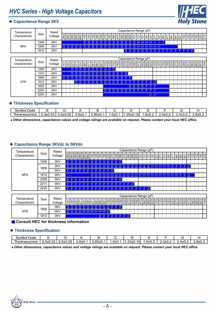
� Capacitance Range 2KV
Symbol Code S O A B C D E F G HThickness(mm) 0.3±0.03 0.5±0.05 0.6±0.1 0.85±0.1 1.0±0.1 1.25±0.15 1.6±0.2 2.0±0.2 2.4±0.2 2.8±0.2
� Thickness Specification
� Other dimensions, capacitance values and voltage ratings are available on request. Please contact your local HEC office.
� Capacitance Range 3KVdc to 5KVdc
2R0
3R3
3R9
5R0
8R2
100
120
150
180
220
270
330
390
470
560
680
820
101
121
151
181
221
271
331
391
471
561
681
821
102
122
152
182
222
272
D D D D D D D D D D D D D D D/E D/E D/E E E E
D D D D D D D D D D D D D D D D D D E/F E/F E/F E/F E/F E/F
D D D D D D D E E F F F F F F F F
TemperatureCharacteristic Size Rated
Voltage
2KV
Capacitance Range (pF)
NP01206 2KV1808 2KV1812
151
181
221
271
331
391
471
561
681
821
102
122
152
182
222
272
332
392
472
562
682
822
103
123
153
183
223
273
333
393
473
563
683
823
104
D D D D D D D D D/E E ED D D D D D D D D E E E F G
D D D D D D D D D D D D D D E F FD D D D D D D D D D E E F F F F F F G H
E E E E F F FD D D D D D E E F F F F F
E/F E/F
1825 2KV2220 2KV2225 2KV
Capacitance Range (pF)
X7R
1206 2KV1210 2KV1808 2KV1812 2KV
TemperatureCharacteristic Size Rated
Voltage2R
03R
33R
95R
08R
08R
210
012
015
018
022
027
033
039
047
056
068
082
010
112
115
118
122
127
133
139
147
156
168
182
110
212
215
218
222
2
D D D D D D D D D D D E E ED D D D D D D D D D D D D D D D D D D E E E/F E/F E/F E/F E/F F F F F FF F F F F F F F F F F F
D D D D D D D D D D D D E/F E/F E/F E/F E/F E/F E/F E/F E/F E/F F F GF F F F F F F F F F F F F FF F F F F F F F F F F F F F F F FF F F F F F F F F F F F F F F F F F F F F
2208 5KV
2220 5KV
Size RatedVoltage
1812 3KV
Capacitance Range (pF)
NP0
1206 3KV
18083KV5KV
2211 5KV
TemperatureCharacteristic
151
181
221
271
331
391
471
561
681
821
102
122
152
182
222
272
332
392
472
562
682
822
103
123
153
183
223
273
333
393
473
563
683
823
104
D D D D D D D D D D D F F FD D D D D/E D/E D/E D/F D/F D/F D/F
E F F F F F F FX7R
18083KV4KV
1812 3KV
Capacitance Range (pF)TemperatureCharacteristic
Size RatedVoltage
Consult HEC for thickness information
Symbol Code S O A B C D E F G HThickness(mm) 0.3±0.03 0.5±0.05 0.6±0.1 0.85±0.1 1.0±0.1 1.25±0.15 1.6±0.2 2.0±0.2 2.4±0.2 2.8±0.2
� Thickness Specification
� Other dimensions, capacitance values and voltage ratings are available on request. Please contact your local HEC office.

� How To Order
SCC SeriesSafety Capacitors rated to 250Vac X1/Y2, X2/Y3 & X2
� Safety Detail of Specifications
The SCC series of X1/Y2, X2/Y3 & X2 safety capacitors are designed specifically for use in modem, facsimile,telephone and other electronic equipment. These parts are compliant to EN/IEC60384-14 and UL60950-1standards. These capacitors are available in NP0 (C0G), SL and X7R dielectrics.
EN 60384-1: 2001EN 60384-14: 2005
Meets the electrical requirements and certification for equipment requiring class X1/Y2 and X2/Y3 devices.
IEC 60950-1 : 2005 Component certified for equipment requiring IEC 60950 compliance
IEC 60384-1: 1999IEC 60384-14: 2005
Component certified for equipment requiring IEC-384 compliance
UL 60950-1: 20072nd edition TNV/SELV Isolation capacitors certified to UL 60950 -1
SCC Series - Safety Capacitors
� Features � Application
SCC 1808 X 102 K 502 T S
- 9 -
� Small size & high capacitance values.� Suitable for reflow soldering.� Surface mount.� RoHS compliant and Lead (Pb) free option.� Safety standard approval by EN/IEC 60384-14
and UL 60950-1.� Certified to:
TUV R50005234, R50103496 & UL E229738TUV R50162550 & UL E229738 for Lead (Pb) free.
� Specially designed for use in modem, facsimile,telephone and other telecommunicat ionequipment, electronic equipment for lightningand surge protection, EMI filtering and isolation.
Product Code
SCC : Safetyapproved MLCC
Chip Size
Ex. :18081812 220822112220 2825
Dielectric
Ex. :N : NP0X : X7RL : SL
CapacitanceUnit : pFEx. :
2R0 : 2.0pF100 : 10×100
471 : 47×101
182 : 18×102
Tolerance
Ex. :J : +/- 5%K : +/-10%M : +/-20%
Class
Ex. :202 : X2302 : X2/Y3502 : X1/Y2602 : X1/Y2 for
SCC2208N,SCC2211N,SCC2220N
Packaging
T : Tape & Reel
B : Bulk
SpecialRequirement Ex. :S : Arc Prevention
CoatingX : Polymer Termination
(SuperTerm)Z : Arc Prevention Coating
& SuperTermG : Lead (Pb) free

W
T
BW B
L
X: Across The Line (Ex.: SCC1808N151K302T)Y : Line By Pass (Ex.: SCC2211X102K502T)
Rated Voltage AC 250Vrms
Temperature CoefficientNP0 : < 30ppm/ Ԩ , -55~+125 Ԩ (EIA Class ǿ )SL: +350~ -1000ppm/°C -55~+85°CX7R : < ± 15% , -55~+125 Ԩ (EIA Class Τ)
Capacitance Range See table below Quality and Dissipation Factor NP0/SL : Q1000ؤ ; X7R : D.F.2.5أ%Climatic Category -55/125/21Insulation Resistance 10Gȍ
Voltage Proof X Capacitor : Applied Voltage 1075Vdc(4.3Ur)Y Capacitor : Applied Voltage 1500Vac
Impulse Y3 : 2.5KV (Compliant to IEC 60950) ; X2 : 2.5KV / Y2 : 5KV for three times Ageing NP0 : 0 % ; SL : 1.5% ; X7R : 1.0 % per decade hr, typical
Y
TYPE L W T (max) B (min) BW (min)
1808 4.60±0.3[.181±.012]
2.00±0.2[.079 ±.008]
2.20[.087]
2.50[.098]
0.20[.008]
1812 4.60±0.3[.181±.012]
3.20±0.3[.126±.012]
2.60[.102]
2.50[.098]
0.20[.008]
2208 5.70±0.4[.220±.016]
2.00±0.2[.079±.008]
2.20 [.087]
4.00 [.157]
0.30[.012]
2211 5.70±0.4[.220±.016]
2.80±0.3[.110±.012]
3.00[.118]
4.00[.157]
0.30[.012]
2220 5.70±0.4[.220±.016]
5.00±0.4[.197±.016]
3.00[.118]
4.00[.157]
0.30[.012]
2825 6.80±0.4[.280±.016]
6.35±0.4[.197±.016]
4.00[.157]
4.00[.157]
0.30[.012]
� Dimensions
� Application Example Circuit
� Summary of Specifications
Unit : mm [inches]
Y Tip & Ring
X
TNV SELV
2nd 1st
SCC Series - Safety Capacitors
- 10 -

SCC Series - Safety Capacitors
- 11 -
� Capacitance Range
� Capacitance Range Lead (Pb) free
‘X’ denotes values that have been tested to a rated voltage of 305VacTUV test report number 28208004 dated 27th May 2010
2R0
5R0
6R8
8R2
100
120
150
180
220
270
330
360
390
470
560
680
820
101
121
131
151
181
221
271
331
391
471
561
681
821
102
122
152
182
222
272
332
472
473
563
x x x x x x x x x x x x
Class Size TemperatureCharacteristic
RatedVoltage Certificated 10
112
113
115
118
122
127
133
139
147
156
168
182
110
212
215
218
222
227
233
239
247
256
268
282
210
312
315
318
322
327
333
339
347
356
368
382
310
412
418
4
TUV/ULX2
250Vrms TUV/ULTUV/ULTUV/UL
2220
SLX7R
NP0X7RNP0X7R
X7R
18081808
1808
250Vrms250Vrms
250Vrms TUV/UL
TUV/ULTUV/UL
CertificatedCapacitance Range (pF)
Class Size TemperatureCharacteristic
RatedVoltage
TUV/UL
1812 X7R 250Vrms TUV/UL
X2/Y3
1808 NP0 250Vrms
180818121812
250Vrms250Vrms
X1/Y2 2208 NP0 250Vrms TUV/UL2208 X7R 250Vrms TUV/UL
2211 X7R 250Vrms TUV/UL2211 NP0 250Vrms TUV/UL
2220 NP0 250Vrms TUV/UL2220 X7R 250Vrms TUV/UL
250Vrms
2R0
5R0
6R8
8R2
100
120
150
180
220
270
330
360
390
470
560
680
820
101
121
131
151
181
221
271
331
391
471
561
681
821
102
122
152
182
222
272
332
472
473
563
x x x x x x x x x x x xX2 2825 X7R 250Vrms TUV
2220 NP0 250Vrms TUV/UL2220 X7R 250Vrms TUV/UL
2211 NP0 250Vrms TUV/UL2211 X7R 250Vrms TUV/UL
2208 NP0 250Vrms TUV/UL2208 X7R 250Vrms TUV/UL
1812 X7R 250Vrms TUV/UL
TUV
X1/Y2
1808 NP0 250Vrms TUV/UL1808 X7R 250Vrms TUV/UL
X2/Y31808 NP0 250Vrms
1812 X7R 250Vrms
TUV/UL1808 X7R 250Vrms TUV/UL
Class Size TemperatureCharacteristic
RatedVoltage Certificated
Capacitance Range (pF)
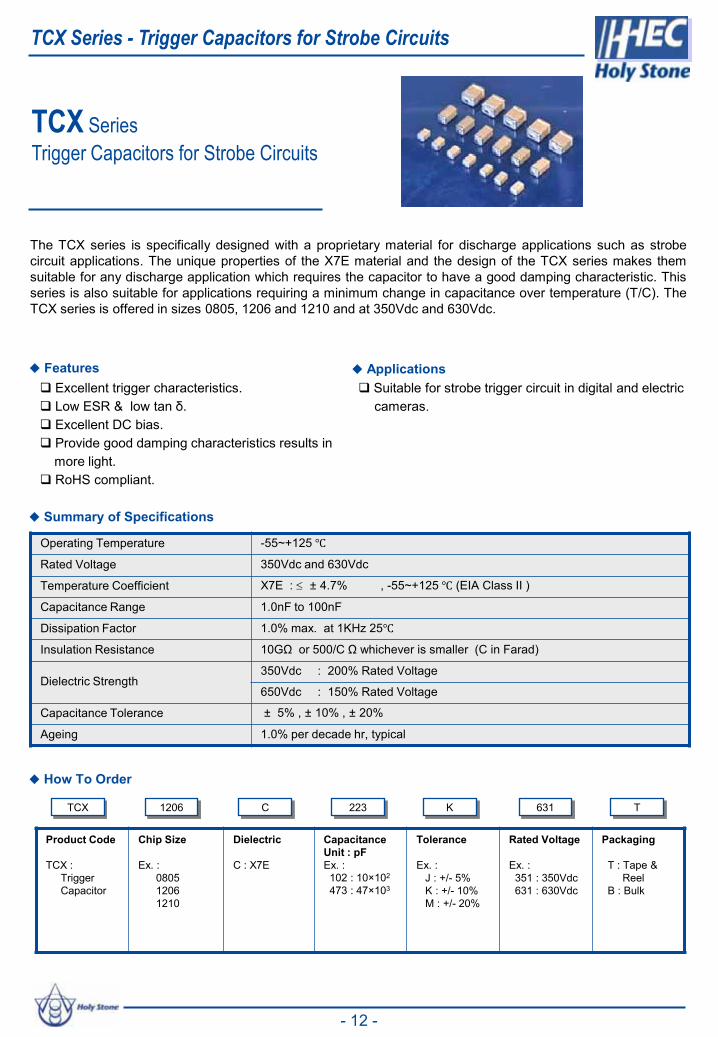
TCX SeriesTrigger Capacitors for Strobe Circuits
� How To Order
Operating Temperature -55~+125 ԨRated Voltage 350Vdc and 630Vdc
Temperature Coefficient X7E : d ± 4.7% , -55~+125 Ԩ (EIA Class II )
Capacitance Range 1.0nF to 100nF
Dissipation Factor 1.0% max. at 1KHz 25ԨInsulation Resistance ��*ȍ��RU�����&�ȍ�ZKLFKHYHU�LV�VPDOOHU���&�LQ�)DUDG�
Dielectric Strength350Vdc : 200% Rated Voltage
650Vdc : 150% Rated Voltage
Capacitance Tolerance ± 5% , ± 10% , ± 20%
Ageing 1.0% per decade hr, typical
� Summary of Specifications
� Features
TCX 1206 C 223 K 631 T
Product Code
TCX : TriggerCapacitor
Chip Size
Ex. :08051206 1210
Dielectric
C : X7E
CapacitanceUnit : pFEx. :102 : 10×102
473 : 47×103
Tolerance
Ex. :J : +/- 5%K : +/- 10%M : +/- 20%
Rated Voltage
Ex. :351 : 350Vdc631 : 630Vdc
Packaging
T : Tape &Reel
B : Bulk
� Applications� Excellent trigger characteristics.� /RZ�(65���ORZ�WDQ�į�� Excellent DC bias.� Provide good damping characteristics results in
more light.� RoHS compliant.
� Suitable for strobe trigger circuit in digital and electric cameras.
The TCX series is specifically designed with a proprietary material for discharge applications such as strobecircuit applications. The unique properties of the X7E material and the design of the TCX series makes themsuitable for any discharge application which requires the capacitor to have a good damping characteristic. Thisseries is also suitable for applications requiring a minimum change in capacitance over temperature (T/C). TheTCX series is offered in sizes 0805, 1206 and 1210 and at 350Vdc and 630Vdc.
TCX Series - Trigger Capacitors for Strobe Circuits
- 12 -

� Characteristics
� Capacitance Range
� Dimensions
W
T
BW B
L
� Application Example Circuit
+-
DSC Strobe Circuit
Trigger Cap.
TYPE L W T (max) B (min) BW (min)
0805 2.00±0.2[.079±.008]
1.25±0.2[.049 ±.008]
1.45[.057]
0.70[.028]
0.20[.008]
1206 3.20±0.3[.126±.012]
1.60±0.2[.063±.008]
1.80[.071]
1.50[.059]
0.30[.012]
1210 3.20±0.3[.126±.012]
2.50±0.2[.098±.008]
1.80 [.071]
1.60 [.063]
0.30[.012]
Unit : mm [inches]
� Other dimensions, capacitance values and voltage ratings are available. Please contact HEC.
TCX Series -Trigger Capacitors for Strobe Circuits
Damping (Trigger) Properties
-4000
-3000
-2000
-1000
0
1000
2000
3000
4000
5000
0 1 2 3 4 5 6 7 8 9 10Time (µs)
Trig
ger
Vol
tage
(V
p)
TCX/1206/223K/630V
X7R/1206/223K/630V
R-C Charge Curv e
0
50
100
150
200
250
300
0 1 2 3 4 5 6 7Time (sec.)
Vol
tage
(V
)
TCX/1206/223K/630V
X7R/1206/223K/630V
- 13 -
Symbol Code S O A B C D E F G HThickness(mm) 0.3±0.03 0.5±0.05 0.6±0.1 0.85±0.1 1.0±0.1 1.25±0.15 1.6±0.2 2.0±0.2 2.4±0.2 2.8±0.2
102
122
152
182
222
272
332
392
472
562
682
822
103
123
153
183
223
273
333
393
473
563
683
823
104
154
224
C C C C C C C C C C C C C C C D D DC C C C D D D E E
D D D D D D D E E ED D D D D D D E E
DielectricCharacteristic Size Voltage
Capacitance Range
X7E
0805 350V
1206350V630V
1210 630V

LDC SeriesLow Distortion Capacitors NP0/X7R Hybrid
LDC 1206 C 103 K 025 T
Product Code
LDC : LowDistortionCapacitor
Chip Size
Ex. :060308051206121018122220
Dielectric
C : X7E
CapacitanceUnit : pFEx. :102 : 10×102
224 : 22×104
Tolerance
Ex. :J : +/- 5%K : +/- 10%M : +/- 20%
Rated Voltage
Ex. :025 : 25Vdc050 : 50Vdc
Packaging
T : Tape &Reel
B : Bulk
Operating Temperature -55~+125 ԨRated Voltage 25V and 50Vdc
Temperature Coefficient X7E : d ± 4.7% , -55~+125 Ԩ (EIA Class II )
Capacitance Range 1nF ~ 270nF
Dissipation Factor For 50V : 1.2% max. at 1KHz 25ԨFor 25V : 2.0% max. at 1KHz 25Ԩ
Insulation Resistance 10Gȍ or 500/C ȍ whichever is smaller
Dielectric Strength 250% Rated Voltage for 5 second @ 50mA max. current
Capacitance Tolerance ± 5% , ± 10% , ± 20%
Ageing 1.0% per decade hr , typical
� How To Order
� Summary of Specifications
� Suitable for telecommunication (ADSL modem),power (inverter for oscillation circuit) & audiocircuits.
� Features � Application � Small size & high capacitance.� Ultra stable T/C for a Class ll.� Excellent bias, high temperature stability &ORZ�WDQ�į�
� High breakdown voltage.� Replacement for film capacitors.� RoHS compliant.
LDC Series - Low Distortion Capacitors
- 14 -
W
T
BW B
L
TYPE L W T (max) B (min) BW (min)
0603 1.60±0.1[.063±.004]
0.80±0.1[.031 ±.004]
0.90[.035]
0.40[.016]
0.15[.006]
0805 2.00±0.2[.079±.008]
1.25±0.2[.049 ±.008]
1.45[.057]
0.70[.028]
0.20[.008]
1206 3.20±0.3[.126±.012]
1.60±0.2[.063±.008]
1.80[.071]
1.50[.059]
0.30[.012]
1210 3.20±0.3[.126±.012]
2.50±0.2[.098±.008]
1.80 [.071]
1.60 [.063]
0.30[.012]
1812 4.60±0.3[.181±.012]
3.20±0.3[.126±.012]
2.20[.087]
2.50[.098]
0.30[.012]
2220 5.70±0.4[.220±.016]
5.00±0.4[.197±.016]
2.20[.087]
3.50[.137]
0.30[.012]
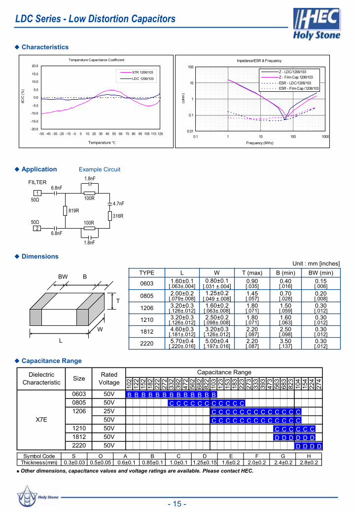
� Characteristics
� Application Example Circuit
FILTER6.8nF
6.8nF
819R
100R
100R
1.8nF
1.8nF
1
2
4.7nF
316R
50ȍ
50ȍ
� Dimensions
� Capacitance Range
Unit : mm [inches]
� Other dimensions, capacitance values and voltage ratings are available. Please contact HEC.
LDC Series - Low Distortion Capacitors
Temperature Capacitance Coefficient
-20.0
-15.0
-10.0
-5.0
0.0
5.0
10.0
15.0
20.0
-55 -45 -35 -25 -15 -5 5 15 25 35 45 55 65 75 85 95 105 115 125
Temperature
dC/C
(%)
X7R 1206/103
LDC 1206/103
Impedance/ESR & Frequency
0.01
0.1
1
10
100
0.1 1 10 100 1000Frequency (MHz)
(oh
m)
Z - LDC/1206/103Z - Film Cap 1206/103ESR - LDC/1206/103ESR - Film Cap /1206/103
Temperature Ԩ
- 15 -
Symbol Code S O A B C D E F G HThickness(mm) 0.3±0.03 0.5±0.05 0.6±0.1 0.85±0.1 1.0±0.1 1.25±0.15 1.6±0.2 2.0±0.2 2.4±0.2 2.8±0.2
102
122
152
182
222
272
332
392
472
562
682
822
103
123
153
183
223
273
333
393
473
563
683
823
104
154
224
274
B B B B B B B B B B B B BC C C C C C C C C C C
C C C C C C C C C C C C CC C C C C C C C C C C C C
C C C C C CD D D D D D
D D D D
DielectricCharacteristic Size Rated
VoltageCapacitance Range
X7E
0603 50V0805 50V1206 25V
50V1210 50V1812 50V2220 50V

� Application
NCC SeriesNormal Chip Capacitors NP0, X7R, X5R,Y5V
� Summary of Specifications
Standard Multilayer Ceramic Chip Capacitors (MLCCs) are available in a full range of sizes and temperature coefficients, with voltage ratings from 6.3V to 50V.
� Surface mount suited for wave and reflow soldering.� Small size and high reliability.� Excellent in high frequency characteristic.� RoHS compliant.
� Suitable for general electronics circuit,telecommunications, personal computersand peripheral, power circuit & mobileapplication etc.
� Features
NCC Series - Normal Chip Capacitors
- 16 -
Operating Temperature -55°C~+125 Ԩ for NP0 and X7R: -55°C ~+85°C for X5R: -30°C~+85°C for Y5VRated Voltage 6.3Vdc to 50Vdc
Temperature Coefficient
NP0 : d ± 30ppm/ Ԩ , -55°C~+125 Ԩ (EIA Class ǿ)X7R : d ± 15% , -55°C~+125 Ԩ (EIA Class Τ)X5R : d ± 15% , -55°C~+85 Ԩ (EIA Class Τ)Y5V: +22%/-82% , -30°C ~ +85°C (EIA Class Τ)
Dissipation Factor NP0 : More than 30pF: Q�����������������S)�DQG�EHORZ���4�������&��& S)�
X7R, X5R and Y5V: please see table 1 on page 39 for detailsInsulation Resistance 10Gȍ or 500/C ȍ� whichever is smallerAgeing NP0:0% ; X7R/X5R: typically 1.0% and Y5V �����SHU�GHFDGH�RI�WLPHDielectric Strength 250% rated voltage
� Dimensions
W
T
BW B
L
TYPE L W T (max) B (min) BW (min)
0201 0.60±0.03[.024±.001]
0.30±0.03[.011 ±.001]
0.33[.013]
0.20[.008]
0.10[.004]
0402 1.00±0.05[.039±.002]
0.50±0.05[.020 ±.002]
0.55[.022]
0.30[.012]
0.15[.006]
0603 1.60±0.10[.063±.004]
0.80±0.10[.031 ±.004]
0.90[.035]
0.40[.016]
0.15[.006]
0805 2.00±0.20[.079±.008]
1.25±0.20[.049 ±.008]
1.45[.057]
0.70[.028]
0.20[.008]
1206 3.20±0.30[.126±.012]
1.60±0.20[.063±.008]
1.80[.071]
1.50[.059]
0.30[.012]
Product Code
C : MLCCMultilayerCeramic Capacitor
Chip Size
Ex. :0201 0402 0603 08051206
Dielectric
Ex. :N : NP0X : X7RB : X5RY : Y5V
CapacitanceUnit : pFEx. :
102 : 10×102
473 : 47×103
104 : 10×104
Tolerance
Ex. :C : +/- 0.25pFD : +/- 0.50pFF : +/- 1%G : +/- 2%J : +/- 5%K : +/- 10%M : +/- 20%Z : +80/-20%
Rated Voltage
Ex. :007 : 6.3Vdc010 : 10Vdc016 : 16Vdc025 : 25Vdc050 : 50Vdc
Packaging
T : Tape & ReelB : Bulk
� How To Order
C 0402 B 104 M 010 T

� Capacitance Range
NCC Series - Normal Chip Capacitors
-17 -
� Other dimensions, capacitance values and voltage ratings are available. Please contact HEC.
Symbol Code S O A B C D E F G HThickness(mm) 0.3±0.03 0.5±0.05 0.6±0.1 0.85±0.1 1.0±0.1 1.25±0.15 1.6±0.2 2.0±0.2 2.4±0.2 2.8±0.2
101
121
151
181
221
271
331
391
471
561
681
102
122
152
182
222
272
332
392
472
562
682
822
103
123
153
183
223
273
333
393
473
563
683
823
104
154
224
334
474
684
OO O O O O O O O O O O
O O O O OO O O O O O O O O O O O O O O O O O O O O O O O
B B B B B B B B B B B B B B B B B B B B B B B B B B B B B B B B B B B B B BB B B B B B B B B B B B B B B B B B B B B B B B B B B B B B B B B B B BB B B B B B B B B B B B B B B B B B B B B B B B B B B B B B B B B B
B B B B B B B B B B B B B B B B B B B B B B B B B B B B B B D D DB B B B B B B B B B B B B B B B B B B B B B B B B B B B B B D DB B B B B B B B B B B B B B B B B B B B B B B B B B B B B C D
B B B C DB B B C DB B B C D
DielectricCharacteristic Size Rated
Voltage
0402
10V16V25V50V16V25V50V
080516V25V50V
0603
120616V25V50V
X7R
Capacitance Range (pF)10
222
247
210
322
347
310
422
447
4
O OOB B BB B BBB B BB B BB B BB B BB B BB B B
Capacitance RangeDielectricCharacteristic Size Rated
Voltage
25V50V
120616V25V50V
Y5V
0402 10V16V
060316V25V50V
080516V
0R5
1R0
1R5
2R0
3R0
4R0
5R0
6R0
7R0
8R0
9R0
100
120
150
180
220
270
330
390
470
560
680
820
101
121
151
181
221
271
331
391
471
561
681
821
102
122
152
182
222
272
332
O O O O O O O O O O O O O O O O O O O O OB B B B B B B B B B B B B B B B B B B B B B B BB B B B B B B B B B B B B B B B B B B B B B B B0805 50V
Capacitance Range (pF)
NPO
DielectricCharacteristic Size Rated
Voltage
0402 50V0603 50V
273
333
393
473
563
683
823
104
154
224
334
474
684
SO O
O O OO O O O O O O OO O O O O O O O
B BB B B B B B
BB B B B B BB B B B B
B
X5R
DielectricCharacteristic Size Rated
Voltage
6.3V10V
6.3V10V
16V25V
0402
16V25V
0603
Capacitance Range (pF)
0201 6.3V

� Surface mount, suited for wave and reflowsoldering.
� High reliability.� Small size and high capacitance value. � Excellent high frequency characteristics.� RoHS compliant.
HCC SeriesHigh Capacitance MLCC - 1uF and above
� Summary of Specifications
� Features� Application
� Ideal for smoothing and decoupling circuits� Suitable for DC-DC converter , personal
computer and peripherals, telecommunicationand general electronic equipment
HCC Series - High Capacitance MLCC
- 18 -
Operating Temperature -55°C~+125 Ԩ for X7R: -55°C ~+85°C for X5R: -30°C~+85°C for Y5VRated Voltage 6.3Vdc to 50Vdc
Temperature CoefficientX7R : d ± 15% , -55°C~+125 Ԩ (EIA Class Τ)X5R : d ± 15% , -55°C~+85 Ԩ (EIA Class Τ)Y5V: +22%/-82% , -30°C ~ +85°C (EIA Class Τ)
Dissipation Factor : X7R, X5R and Y5V: Please see table 1 on page 39 for detailsInsulation Resistance 10Gȍ or 500/C ȍ� whichever is smallerAgeing X7R/X5R: Typically 1.0% and Y5V �����SHU�GHFDGH�RI�WLPHDielectric Strength 250% Rated Voltage
� DimensionsTYPE L W T (max) B (min) BW (min)
0402 1.00±0.05[.039±.002]
0.50±0.05[.020 ±.002]
0.55[.022]
0.30[.012]
0.15[.006]
0603 1.60±0.10[.063±.004]
0.80±0.10[.031 ±.004]
0.90[.035]
0.40[.016]
0.15[.006]
0805 2.00±0.20[.079±.008]
1.25±0.20[.049 ±.008]
1.45[.057]
0.70[.028]
0.20[.008]
1206 3.20±0.30[.126±.012]
1.60±0.20[.063±.0108
1.80[.071]
1.50[.059]
0.30[.012]
1210 3.20±0.30[.126±.012]
2.50±0.20[.098±.008]
2.60 [.102]
1.60 [.063]
0.30[.012]
1812 4.60±0.3[.181±.012]
3.20±0.3[.126±.012]
3.00[.118]
2.50[.098]
0.30[.012]
2220 5.7±0.40[.220±.016]
5.00±0.40[.197±.016]
3.00 [.118]
3.50 [.137]
0.30[.012]
W
T
BW B
L
Product Code
C : MLCCMultilayerCeramic Capacitor
Chip Size
Ex. :0402 0603 0805 1206 1210 18122220
Dielectric
Ex. : X : X7RB : X5RY : Y5V
CapacitanceUnit : pFEx. :
105 : 10×105
106 : 10×106
226 : 22×106
Tolerance
Ex. :J : +/- 5%K : +/- 10%M : +/- 20%Z : +80/-20%
Rated Voltage
Ex. :007 : 6.3Vdc010 : 10Vdc016 : 16Vdc025 : 25Vdc035 : 35Vdc050 : 50Vdc
Packaging
T : Tape& Reel
B : Bulk
� How To OrderC 0805 B 106 M 010 T

� Capacitance Range
HCC Series - High Capacitance MLCC
- 19 -
� Other dimensions, capacitance values and voltage ratings are available. Please contact HEC.
Symbol Code S O A B C D E F G HThickness(mm) 0.3±0.03 0.5±0.05 0.6±0.1 0.85±0.1 1.0±0.1 1.25±0.15 1.6±0.2 2.0±0.2 2.4±0.2 2.8±0.2
Code VDC 16V 35V105 1uF B B B B D D D D D E E D D D D F F225 2.2uF B B B D D D E E E F F F475 4.7uF D D E E F F F106 10uF E F F G
121025V 35V
060316V10V6.3V 10V 25V 6.3V 16V
Size 0805 18121206 2220X7R (X) Series
25V 10V 35V50V 35V50V 16V 25V
Code VDC105 1uF O O B B B B B D225 2.2uF B B B D D D475 4.7uF B B D D D D D106 10uF D D D D E E E E E226 22uF D D E F F
Y5V (Y) Series
50V50V 10V 35V16V 25V 35V 50V 6.3V 10V 16V 25V16V 25V 6.3V 10V 16V 25V6.3V 10V 6.3 10VSize 0402 0603 0805 1206 1210
Code VDC105 1uF O O B B B B D D D D D E E225 2.2uF O B B B D D D D E E E E E/F F D475 4.7uF B B D D D D E E E E F F F106 10uF B D D D E E E E F F F F226 22uF D D E E E G G G476 47uF E E107 100uF G
35V12060603 0805 1210
16V 25V 50V
X5R (B) SeriesSize 0402
6.3V 10V 6.3V 10V 6.3V 10V 16V 25V 10V6.3V 10V 16V 25V 16V 25V35V 50V 6.3V

HCN SeriesHigh Capacitance NP0 - 1nF and above
� Small size & high capacitance.� Suitable for wave and reflow soldering.� Excellent characteristics and tight tolerance.� ([FHOOHQW�ELDV��KLJK�WHPSHUDWXUH�VWDELOLW\��ORZ�WDQ�į�� Replace film capacitors.� RoHS compliant.
C 1206 N 103 J 025 T
Product Code
C : MLCCMultilayer Ceramic Capacitor
Chip Size
0603 0805 1206 1210 1812
Dielectric
N : NP0
CapacitanceUnit : pFEx. :102 : 10×102
103 : 10×103
124 : 12×104
Tolerance
Ex. :F : +/- 1%G : +/- 2%J : +/- 5%
Rated Voltage
Ex. :016 : 16Vdc025 : 25Vdc050 : 50Vdc
Packaging
T : Tape &Reel
B : Bulk
Operating Temperature -55~+125 ԨRated Voltage 16V to 50Vdc
Temperature Coefficient NP0 : d 30ppm/Ԩ, -55~+125 Ԩ (EIA Class ǿ )
Capacitance Range 1nF ~ 220nF
Dissipation Factor Q ��������DW��.+]���ԨInsulation Resistance 10Gȍ or 500/C ȍ whichever is smaller (C in Farad)
Dielectric Strength 250% rated voltage for 5 second @ 50mA max. current
Ageing 0% per decade hr
� How To Order
� Summary of Specifications
� Features � Application
� Suitable for ADSL filter circuits, cable modem andcoupling circuits, general telecommunications use,power (inverter for oscillation circuit) and audiocircuits.
HCN Series - High Capacitance NP0
- 20 -

� Characteristics
� Application Example Circuits
� Dimensions
� Capacitance Range
680uH
Tx Filter560pF
560pF
1.5nF 2.7nF
4.75KR
4.75KR680uH
348R
348R
1
2
Unit : mm [inches]
Z/ESR & Frequency
0.001
0.01
0.1
1
10
100
1000
10000
100000
0.1 1 10 100 1000 10000 100000Frequency (KHz)
Ohm
Z- MLCC- NPO 1812/683ESR-MLCC NPO 1812/683Z- Film Cap 1812/683ESR- Film Cap 1812/683
Temperature Capacitance Coefficient
-5000
-4000
-3000
-2000
-1000
01000
2000
3000
4000
5000
-55 -45 -35 -25 -15 -5 5 15 25 35 45 55 65 75 85 95 105 115 125
Temperature(ഒ)
dC/C
(ppm
)
NPO-1812/683Film-1812/683
Rx Filter1.5nF
1.5nF
1.8nF
1.8nF
1.8nF
1.8nF
3.3nF
3.3nF
6.8nF
680uH 680uH 680uH
4.7nF 18nF 4.2KR
4.2KR100nF
2
1
TYPE L W T (max) B (min) BW (min)0603 1.60+/-0.1
[.063+/-.004]0.80+/-0.1
[.031+/-.004]0.90[.039]
0.40[.016]
0.15[.006]
0805 2.00±0.2[.079±.008]
1.25±0.2[.049 ±.008]
1.40[.055]
0.70[.028]
0.20[.008]
1206 3.20±0.3[.126±.012]
1.60±0.2[.063±.008]
1.80[.071]
1.50[.059]
0.30[.012]
1210 3.20±0.3[.126±.012]
2.50±0.2[.098±.008]
2.20 [.087]
1.60 [.063]
0.30[.012]
1812 4.60±0.3[.181±.012]
3.20±0.3[.126±.012]
2.20[.087]
4.00[.157]
0.20[.008]
HCN Series - High Capacitance NP0
W
T
BW B
L
- 21 -
� Other dimensions, capacitance values and voltage ratings are available. Please contact HEC.
Symbol Code S O A B C D E F G HThickness(mm) 0.3±0.03 0.5±0.05 0.6±0.1 0.85±0.1 1.0±0.1 1.25±0.15 1.6±0.2 2.0±0.2 2.4±0.2 2.8±0.2
102
122
152
182
222
272
332
392
472
562
682
822
103
123
153
183
223
273
333
393
473
563
683
823
104
124
154
224
B B B B B B BB B B B B B BB B B B B B BB B B B C/D D D D D D D D DB B B B C/D D D D D D D D DB B B B C/D D D D D D D D DB B B B B B B B B B B B B D D D D EB B B B B B B B B C D D DB B B B B B B B B C D D EC C C C C C C C C C C C C D D D D D E E EC C C C C C C C C C C C C D E E FC C C C C C C C C C C C C D E E FD D D D D D D D D D D D D D D D E E E E F F F F F FD D D D D D D D D D D D D D D D E E E E FD D D D D D D D D D D D D D D D E E E E F
181216V25V50V
16V25V50V
121016V25V50V
NPO
060316V25V50V
080516V25V50V
1206
DielectricCharacteristic Size Voltage
Capacitance Range
HCX SeriesHigh Capacitance X7R - 100nF and above
Product Code
C : MLCCMultilayerCeramic Capacitor
Chip Size
Ex. :1210 1812 1825 2220 2225
Dielectric
X : X7R
CapacitanceUnit : pFEx. :
102 : 10×102
224 : 22×104
105 : 10×105
Tolerance
Ex. :K : +/- 10%M : +/- 20%
Rated Voltage
Ex. :050 : 50Vdc101 : 100Vdc
Packaging
T : Tape &Reel
B : Bulk
SpecialRequirement Ex. :O : Arc
PreventionCoating
X : FlexibleTermination (Super Term)
Operating Temperature -55~+125 ԨRated Voltage 50V to 100Vdc
Temperature Coefficient X7R : d ± 15% at -55~+125 Ԩ (EIA Class II )
Capacitance Range 100nF ~ 10uF
Dissipation Factor 2.5% max. at 1KHz 25ԨInsulation Resistance 10Gȍ or 500/C ȍ whichever is smaller (C in Farad )
Dielectric Strength50V : 250% rated voltage for 5 second @ 50mA max. current
100V :200% rated voltage for 5 second @ 50mA max. current
Capacitance Tolerance ± 10% , ± 20%
Ageing 1.0% per decade hr , typical
� How To Order
� Summary of Specifications
� Features � Application
� DC-DC converters (filter)� Industrial controls � Power supplies � Surge protection
� Rated working voltage of 50V and 100Vdc.� Small size & high capacitance.� ([FHOOHQW�ELDV��KLJK�WHPSHUDWXUH�VWDELOLW\��ORZ�WDQ�į�� Low ESR and excellent ripple current characteristics� RoHS compliant
HCX Series - High Capacitance X7R
C 1210 X 225 K 101 T X
- 22 -
TYPE L W T (max) B (min) BW (min)
1210 3.20±0.3[.126±.012]
2.50±0.2[.098±.008]
2.60 [.102]
1.60 [.063]
0.30[.012]
1812 4.60±0.3[.181±.012]
3.20±0.3[.126±.012]
3.00[.118]
2.50[.098]
0.30[.012]
1825 4.60±0.3[. 181±.012]
6.35±0.4[.250±.016]
3.00[.118]
2.50[.137]
0.30[.012]
2220 5.70±0.4[.220±.016]
5.00±0.4[.197±.016]
3.00[.118]
3.50[.137]
0.30[.012]
2225 5.70±0.4[.220±.016]
6.35±0.4[.250±.016]
3.00[.118]
3.50[.137]
0.30[.012]
W
T
BW B
L
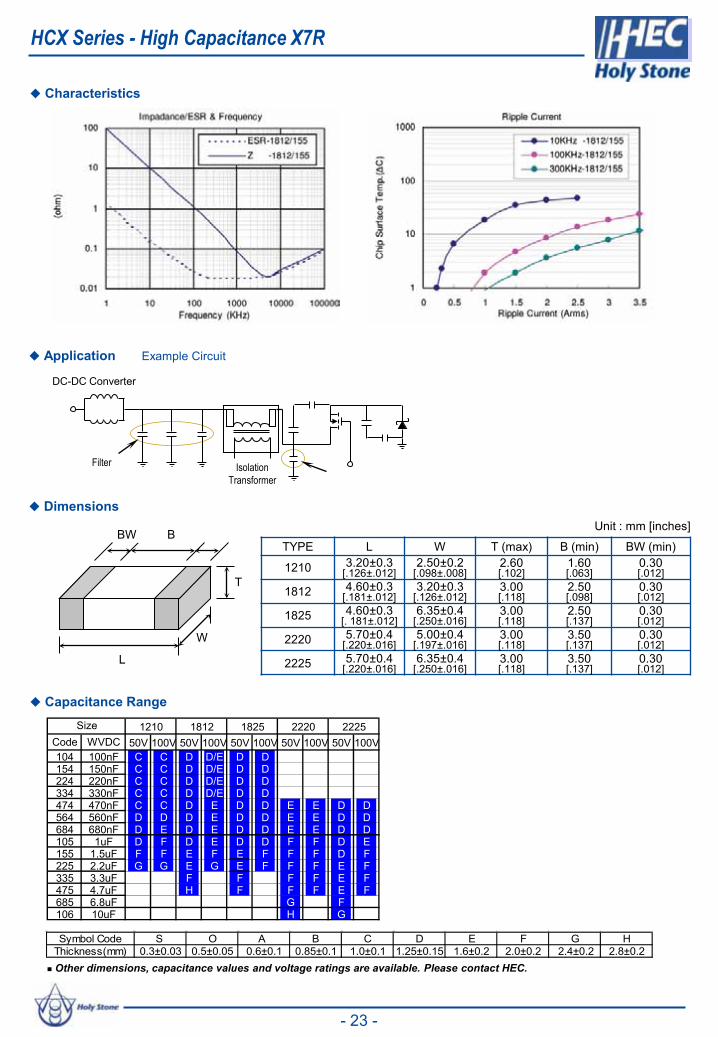
� Characteristics
� Application Example Circuit
� Dimensions
� Capacitance Range
Filter Isolation Transformer
DC-DC Converter
Unit : mm [inches]
� Other dimensions, capacitance values and voltage ratings are available. Please contact HEC.
HCX Series - High Capacitance X7R
- 23 -
Symbol Code S O A B C D E F G HThickness(mm) 0.3±0.03 0.5±0.05 0.6±0.1 0.85±0.1 1.0±0.1 1.25±0.15 1.6±0.2 2.0±0.2 2.4±0.2 2.8±0.2
Code WVDC104 100nF C C D D/E D D154 150nF C C D D/E D D224 220nF C C D D/E D D334 330nF C C D D/E D D474 470nF C C D E D D E E D D564 560nF D D D E D D E E D D684 680nF D E D E D D E E D D105 1uF D F D E D D F F D E155 1.5uF F F E F E F F F D F225 2.2uF G G E G E F F F E F335 3.3uF F F F F E F475 4.7uF H F F F E F685 6.8uF G F106 10uF H G
Size 1210 1812 1825 2220 222550V 100V 50V 100V 50V 100V 50V 100V 50V 100V

Product Code
C : MLCCMultilayerCeramic Capacitor
Chip Size
Ex. :0805 1206 1210 1812 2220
Dielectric
Ex. :X : X7RE : Y5U
CapacitanceUnit : pFEx. :
103 : 10×103
474 : 47×104
Tolerance
Ex. :K : +/- 10%M : +/- 20%
Rated Voltage
Ex. :251 : 250Vdc
Packaging
T : Tape & Reel
B : Bulk
SAC SeriesTip & Ring Capacitors
� How To Order
� Summary of Specifications
� FeaturesTelephone lines use a DC voltage of 48 voltsand pass the subscriber’s AC signal pulse of 15to 25Hz at 70 to 90Vrms. These MLCC Tip &Ring capacitors replace bulky leaded filmcapacitors and offer excellent frequencyresponse, low ESR and improved temperaturecharacteristics. Ideal for telecommunication andmodem applications.
� Small size & high capacitance.� Suitable for wave and reflow soldering.� Surface mount.� Low ESR characteristics & improved temperature
performance.� RoHS compliant.
SAC Series -Tip & Ring Capacitors
C 1812 X 474 M 251 T
- 24 -
Operating Temperature X7R : -55~+125 Ԩ , Y5U : -30~+85 ԨRated Voltage 250Vdc
Temperature CoefficientY5U : d +22 /-56 % , -30~+85 Ԩ (EIA Class II )
X7R : d ± 15% , -55~+125 Ԩ (EIA Class II )
Capacitance RangeY5U :10nF ~ 1.0uF
X7R :180pF ~ 2.2uF
Dissipation Factor Y5U : D.F.4.0أ% ; X7R : D.F.2.5أ%
Insulation Resistance 10Gȍ or 500/C ȍ whichever is smaller
Dielectric Strength 200% rated voltage for 5 second @ 50mA max. current
Ageing Y5U: 4.0 %; X7R: 1.0 % per decade hr , typical

� Capacitance Range
W
T
BW B
L
Ring
Tip
Ring
Tip0.47uF
200ms/DIV
-48Vdc
� Dimensions
� Application Example Circuit
� Characteristics
TYPE L W T (max) B (min) BW (min)0805 2.00±0.2
[.079±.008]1.25±0.2
[.049 ±.008]1.45[.043]
0.70[.028]
0.20[.008]
1206 3.20±0.3[.126±.012]
1.60±0.2[.063±.008]
1.80[.071]
1.50[.059]
0.30[.012]
1210 3.20±0.3[.126±.012]
2.50±0.2[.098±.008]
2.60 [.102]
1.60 [.063]
0.30[.012]
1812 4.60±0.3[.181±.012]
3.20±0.3[.126±.012]
3.00[.118]
2.50[.098]
0.30[.012]
2220 5.70±0.4[.220±.016]
5.00±0.4[.197±.016]
3.00[.118]
3.50[.137]
0.30[.012]
Unit : mm [inches]
SAC Series - Tip & Ring Capacitors
Temperature Capacitance Coef f icient
-80-70
-60-50
-40-30-20
-100
1020
-55 -35 -15 5 25 45 65 85 105 125Temperature (C)
Cap
acita
nce
Cha
nge
(%)
X7R 1812/474Y5U 1812/474
X7R Impedance/ESR & Frequency
0.01
0.1
1
10
100
1000
10000
0.1 1 10 100 1000 10000 100000Frequency (KHz)
(oh
m)
X7R 1812/474 -ZX7R 1812/474 -ESRY5U 1812/474 -ZY5U 1812/474 -ESR
- 25 -
Subscribers AC Signal
� Other dimensions, capacitance values and voltage ratings are available. Please contact HEC.
Symbol Code S O A B C D E F G HThickness(mm) 0.3±0.03 0.5±0.05 0.6±0.1 0.85±0.1 1.0±0.1 1.25±0.15 1.6±0.2 2.0±0.2 2.4±0.2 2.8±0.2
181
221
271
331
471
681
102
152
182
222
332
472
562
682
103
153
223
273
333
393
473
563
683
823
104
154
224
334
474
564
684
824
105
155
225
B/CB/CB/CB/CB/CB/CB/CB/CB/CB/CB/CB/CB/CB/CB/CB/C D D DB/CB/CB/CB/CB/CB/CB/CB/CB/CB/CB/CB/CB/CB/CB/CB/CB/CB/CB/CB/CB/CC/DD/ED/ED/E
C C C C C C C C C C D D DD D D D D D D/ED/ED/ED/ED/ED/ED/ED/E E E E F G
E E E E E E E E E F HD D D D D D D D D D D D D E E E E F G
DielectricCharacteristic Size Voltage
Capacitance Range
1812 250V2220 250V
Y5U 1812 250V
X7R
0805 250V1206 250V1210 250V
HBC Series Low-Loss, High Frequency Snubber Capacitors
� Low stable ESR at high frequency.� Ultra stable NP0 performance.� Suitable for solder wave and reflow soldering. � ROHS compliant.� High peak to peak voltage capability.
HBC 1206 N 100 J 501 T
Product Code
HBC : Low-loss High Frequency Capacitors
Chip Size
Ex. :1206 1210
Dielectric
Ex. :N : NP0
CapacitanceUnit : pFEx. :100 : 10×100
101 : 10×101
102 : 10×102
Tolerance
Ex. :F : ±1%G : ±2% J : ± 5%K : ±10%
Rated VoltageEx. :501 : 500Vdc631 : 630Vdc
Packaging
T : Tape & Reel
B : Bulk
HBC Series - Low-Loss, High Frequency Snubber Capacitors
Operating Temperature -55~+125 ԨRated Voltage 500V and 630Vdc
Temperature Coefficient d ± 30ppm at -55~+125 ԨCapacitance Range 10pF ~ 2700pF
Dissipation Factor 0.1% max. at 1MHz 25ԨInsulation Resistance 10Gȍ
Dielectric Withstanding 1.5 ×WVDC for 5 sec
Capacitance Tolerance F, G, J, K
Ageing None
Piezo Effects None
dv/dt rating >6KV/µ second
� How To Order
� Summary of Specifications
� High frequency pulse circuits.� Lighting ballast snubber circuits. � DC-DC converters.� High dv/dt rating.
� Features � Application
- 26 -

TYPE L W T (max) B (min) BW (min)
1206 3.20±0.3 1.60±0.2 1.80 1.50 0.30
1210 3.20±.30 2.50±0.2 2.60 1.60 0.30
W
T
BW B
L
HBC Series - Low-Loss, High Frequency Snubber Capacitors
� Characteristics Peak to Peak Voltage
� Dimensions
Unit : mm [inches]
- 27 -
AC Voltage Pulsed Voltage
DC + AC Voltage
0V
DC + Pulsed Voltage
0V
= peak to peak voltage
� Capacitance Range
� Other dimensions, capacitance values and voltage ratings are available. Please contact HEC.
100
120
150
180
220
270
330
390
470
560
680
820
101
121
151
181
221
271
331
391
471
561
681
821
102
122
152
182
222
272
684
824
105
155
225Dielectric
CharacteristicSize Voltage
Capacitance Range
500V1210 630V
630V1210
NP0
1206 500V1206
To convert a DC voltage rating to maximum peak to peak voltage a conversion factor of 1.25 : 1 should beUsed. For example : 500VDC rating = 500/1.25 = 400V peak to peak voltage where peak to peak is definedas below.

HTC SeriesHigh Temperature CapacitorsX8R rated to +150°C
� Rated voltages from 25V to 250V.� Stable temperature coefficient at temperatures
up to 150°C. Near zero loss of capacitance at peak temperature (see chart).
� Fully RoHS compliant.� Available with flexible termination (Super Term)
to minimize mechanical / thermal stress effects.
HTC 1206 H 103 K 025 T
Product Code
HTC :HighTemperatureCapacitor
Chip Size
Ex. : 0603 08051206 1210
Dielectric
Ex. :X8R
CapacitanceUnit : pF
Ex. :102:10×102
224:22×104
Tolerance
Ex. :J : +/- 5%K : +/- 10%M : +/- 20%
Rated Voltage
Ex. :025:25Vdc050:50Vdc101:100Vdc251:250Vdc
Packaging
T : Tape &Reel
B : Bulk
Special Requirement
Ex. :X:Super TermO:Arc Prevention
Coating
HTC Series- High Temperature Capacitors
Operating Temperature -55~+150 ԨRated Voltage 25V ~ 250Vdc
Temperature Coefficient X8R : d ± 15% , -55~+150 Ԩ (EIA Class II )
Capacitance Range 180pF ~ 390nF
Dissipation Factor 2.5 % max. at 1KHz 25ԨInsulation Resistance 100Gȍ or 1000/C ȍ whichever is smaller at 25Ԩ
Dielectric Strength< 200V : 250% rated voltage for 5 second @ 50mA max. current
200~500V : 150% rated voltage for 5 second @ 50mA max. current
Capacitance Tolerance ± 5% , ± 10% , ± 20%
Ageing 2.0% per decade hr, typical
� How To Order
� Summary of Specifications
� Suitable for automotive, oil exploration(drilling and logging) and other demandinghigh temperature environments andapplications.
� Instrumentation and other equipmentcircuit operating at high temperatures.
� Features � Applications
- 28 -
X

W
T
BW B
L
TYPE L W T (max) B (min) BW (min)
0603 1.60±0.1[.063±.004]
0.80±0.1[.031 ±.004]
0.90[.039]
0.40[.016]
0.15[.006]
0805 2.00±0.2[.079±.008]
1.25±0.2[.049 ±.008]
1.45[.057]
0.70[.028]
0.20[.008]
1206 3.20±0.3[.126±.012]
1.60±0.2[.063±.008]
1.80[.071]
1.50[.059]
0.30[.012]
1210 3.20±0.3[.126±.012]
2.50±0.2[.098±.008]
1.80 [.071]
1.60 [.063]
0.30[.012]
� Characteristics
� Dimensions
� Capacitance Range
Unit : mm [inches]
� Other dimensions, capacitance values and voltage ratings are available. Please contact HEC.
- 29 -
X8R-1206 / 100nF
-25.0
-20.0
-15.0
-10.0
-5.0
0.0
5.0
10.0
15.0
20.0
-55 -40 -25 -10 5 20 35 50 65 80 95 110 125 140
dC/C
(%
)
150
HTC Series - High Temperature Capacitors
181
221
271
331
391
471
561
681
102
122
152
182
222
272
332
392
472
562
682
103
123
153
183
223
273
333
393
473
563
683
104
124
154
184
224
274
334
394
474
564
684
105
155
225
50V
X8R
0603
0805
25V50V
25V
250V
121050V
1206
25V
100V
100V250V
100V250V25V50V
TemperatureCharacteristic Size Rated
VoltageCapacitance Range (pF)
� How To Order
LCC SeriesLarge Size NP0 & X7R MLCC Capacitors50V – 8KV
Operating Temperature -55~+125 ԨRated Voltage 50Vdc to 8KVdc
Temperature CoefficientNP0 : d ± 30ppm/ Ԩ , -55~+125 Ԩ (EIA Class ǿ )X7R : d ± 15% , -55~+125 Ԩ (EIA Class Τ )
Capacitance Range NP0 :100pF to 820nF ; X7R :1000pF to 33uFDissipation Factor NP0 : Q1000ؤ ; X7R : D.F.2.5أ%Insulation Resistance 10Gȍ or 500/C ȍ� whichever is smaller (C in Farad )
Ageing NP0:0% ; X7R: 1.0 % per decade of time
Dielectric StrengthV d 500V : 200% rated voltage500V d V � 1000V : 150% rated voltageV t1000V : 120% rated voltage
� Summary of Specifications
� Optimized internal design offers the highest possiblevoltage rating up to 8KVdc.
� Capacitance range from 470pF - 33uF and case sizesfrom 1515 – 7565.
� Available with proprietary surface coating for arcprevention
� Available with flexible termination (Super Term) tominimize the effects of mechanical stress.
� High reliability screening is available.� Pd/Ag, 100% Sn and 90/10 Sn/Pb terminations available.� RoHS compliant.
� Voltage multipliers� Power supplies� DC-DC converters� Surge protection� Industrial control circuits� Isolation� Ballast� Snubber � Custom applications
Product CodeC: MLCC
MultilayerCeramic Capacitor
Chip Size
EX.:1515 2520 3530 3640 4540 555065607565
Dielectric
Ex.:N: NP0X: X7R
CapacitanceUnit : pFEx.:100:10×100
471:47×101
102:10×102
Tolerance
Ex.:C:+/-0.25pFD:+/-0.50pFJ:+/- 5%K:+/-10%M:+/-20%
Rated Voltage Ex.:050:50Vdc251:250Vdc631:630Vdc102:1000Vdc
Packaging
Ex.:T: Tape
& ReelW: Waffle
PackB: Bulk
Termination
Ex.:S:Solderable
AgP:Pd/AgN: 100%
Sn PlatedW:90/10
Sn/Pb Plated
Testing RequirementEx.:S:Standard ElectricalH:Hi-Reliability
SpecialRequirementEx.:Blank:StandardO: Arc PreventionCoatingX: Flexible Termination (Super Term)Z: Arc Prevention and SuperTerm
LCC Series - Large Size MLCC Capacitors
� Applications.� Features
C 2520 X 103 K 102 T N S X
- 30 -

� Dimensions
� Capacitance Range
TYPE L W T (max) B (min) BW (min)
1515 3.80±0.50[.15±.020]
3.80±0.50[.15 ±.020]
3.20[.126]
1.60[.059]
0.30[.012]
2520 6.35±0.50[.25±.020]
5.00±0.50[.20±.020]
3.20[.126]
4.00 [.157]
0.30[.012]
3530 8.90±0.50[.35±.020]
7.60±0.50[.30±.020]
5.00 [.200]
5.50 [.217]
0.30[.012]
3640 9.20±0.50[.36±.020]
10.2±0.50[.40±.020]
5.00 [.200]
6.00 [.236]
0.30[.012]
4540 11.5±0.50[.45±.020]
10.2±0.50[.40±.020]
5.00 [.200]
7.50 [.295]
0.30[.012]
5550 14.0±0.50[.55±.020]
12.7±0.50[.50±.020]
5.00 [.200]
9.00 [.354]
0.30[.012]
6560 16.5±0.50[.65±.020]
15.3±0.50[.60±.020]
5.00 [.200]
11.50 [.453]
0.30[.012]
7565 19.0±0.50[.750±.020]
16.5±0.50[.65±.020]
5.00 [.200]
14.00 [.551]
0.30[.012]
Unit : mm [inches]
� All values are capacitance EIA codes.� Other dimensions, capacitance values and voltage ratings are available. Please contact HEC.
LCC Series-Large Size Multilayer Ceramic Chip Capacitors
50V 100V 200V 500V 1KV 2KV 3KV 4KV 5KV 8KVNPO 473 393 363 103 222 821X7R 225 105 474 124 473 682NPO 823 683 563 473 103 392 222 102 471X7R 475 225 474 224 473 153 472 222 102NPO 154 134 104 823 253 103 472 332 102 471X7R 106 475 225 824 224 473 183 822 472 102NPO 224 184 124 104 373 153 562 362 122 561X7R 126 565 225 105 274 683 273 153 103 182NPO 284 244 184 154 483 203 962 472 152 621X7R 156 685 225 125 394 104 393 223 153 392NPO 364 304 224 184 683 273 153 562 182 681X7R 186 825 275 225 474 124 823 333 223 562NPO 654 484 404 304 104 423 223 682 332 821X7R 226 186 106 335 105 224 104 563 333 103NPO 844 674 504 474 134 553 283 103 472 102X7R 336 226 186 475 125 364 154 823 473 153
6560
7565
Capacitance maximum
3530
3640
4540
5550
2520
1515
DielectricSize
W
T
BW B
L
*Soldering and handling precautions:Large ceramic capacitors are more prone to thermal and mechanical cracks. To minimize mechanical cracks, capacitors have to behandled carefully in the original waffle pack container, carrier tape or other suitable container. Care must be taken that ceramic chips donot come into contact with one another causing chip outs, cracks or other mechanical damage.The recommended method for soldering large chips is reflow soldering. Wave soldering and manual soldering are not recommended.Ceramic capacitors should be preheated to within 50°C of the peak soldering temperature and then use a maximum 2°C/second ramprate for both heating and cooling. A sudden increase or decrease in temperature during soldering may cause internal thermal cracks.
Available Options:• HEC offers flexible termination (Super Term) for very large chips to minimize mechanical cracks due to board flexing.• To minimize the potential for surface arcing in higher voltage applications, HEC offers the option of a proprietary surface coating.• Pure tin terminated / ROHS compliant products are offered as standard, however, lead (Pb) content plated termination is also available.• Pd/Ag termination is also available as an option for hybrid circuits and other applications.
- 31 -

� Summary of Specifications
Operating Temperature -55 to +125 ԨRated Voltage 50Vdc to 1000Vdc
Temperature Coefficient of Capacitance
NPO : d ± 30ppm/ Ԩ , -55 to +125 Ԩ (EIA Class ǿ )X7R : d ± 15% , -55 to +125 Ԩ (EIA Class Τ )
Capacitance RangeNPO: 1.0nF to 400nFX7R : 27nF to 34uF
Dissipation Factor NPO : Qؤ 1000 at 1KHz
X7R : 2.5%max. at 1KHzInsulation Resistance 10Gȍ or 500/C ȍ� whichever is smallerAging NPO : 0% , X7R : 2.5% per decade of time
Dielectric Withstand Voltage
V d50V ; 250% Rated Voltage100V d V <500V ; 200% Rated Voltage500V d V <1KV ; 150% Rated Voltage
1000V = 120% Rated VoltageTolerance ± 1% & ± 2% tolerances are only available in NPO
� Stacked designs offer the high capacitance similarto tantalum but with the advantage of very low ESR.
� ‘J’, ‘L’ and ‘N’ leaded configurations providemechanical and thermal stress relief.
� Capacitance values up to 34µF� Voltages from 50V to 1000V.� Available in NP0 and X7R dielectrics.� HIREL screening available.� RoHS compliant.
� Power supplies� DC-DC converters� Surge protection� Industrial control circuits � Snubbers� Filtering, smoothing and decoupling applications� HIREL applications� Custom applications
� Features � Application
- 32 -
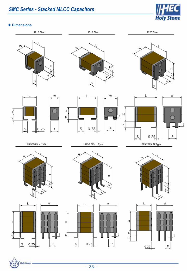
SMC Series Stacked MLCC Capacitors
SMC Series - Stacked MLCC Capacitors
SMC 49 J X 224 K 501
Product Code
SMC:Commercial Size Switchmode Stack Capacitor
Stack and Size
The first digit :# of chips in stack
Second Digit:Chip Size5 : 12106 : 18127 : 22208 : 18259 : 2225
LeadConfiguration
Ex.:J : J Lead for
h=0.070”L : L Lead for
h=0.070”N : Straight LeadP : J Lead for
h=0.045”S : L Lead for
h=0.045”
Material
Ex.:N : NPOX : X7R
Capacitance(pF)
Ex.:103 : 10x103
224 : 22x104
475 : 47x105
Tolerance
Ex.:F : +/-1.0%G : +/-2.0%J : +/-5.0%K : +/- 10%M : +/- 20%
Rated Voltage
Ex.:050 : 50Vdc 101 : 100Vdc201 : 200Vdc 501 : 500Vdc102 : 1000Vdc
Packaging
Ex.:T : Tape &
Reel W : Waffle
pack
Special test Requirement
Ex.:S : Standard electrical testH : Hi-Rel Testing
Special Requirement
Blank :No special requirement01~99 : Customer special requirement
� How To Order T H 01
� Dimensions
SMC Series - Stacked MLCC Capacitors
- 33 -
1812 Size1210 Size 2220 Size
1825/2225 J Type 1825/2225 L Type 1825/2225 N Type

SMC Series - Stacked MLCC Capacitors
- 34 -
EIA Size Code 1210 1812 2220 1825Size Code 15 25 16 26 17 27 18 28
L 3.80 Max[.150 Max]
3.80 Max[.150 Max]
5.50 Max[.217 Max]
5.50 Max[.217 Max]
6.50 Max [.256 Max]
6.50 Max [.256 Max]
5.35±0.50 [.210±.020]
5.35±0.50 [.210±.020]
W (max.) 2.90[.114]
2.90[.114]
4.00[.157]
4.00[.157]
5.50[.217]
5.50[.217]
6.85[.270]
6.85[.270]
H (max.) 2.15[.083]
4.30[.165]
2.10[.083]
4.20[.165]
2.10[.083]
4.20[.165]
2.54[.100]
5.08[.200]
S 1.65±0.50[.065±.020]
1.65±0.50[.065±.020]
1.65±0.50[.065±.020]
1.65±0.50[.065±.020]
1.65±0.50[.065±.020]
1.65±0.50[.065±.020]
1.65±0.50[.065±.020]
1.65±0.50[.065±.020]
P 2.54±0.25[.100±.010]
2.54±0.25[.100±.010]
2.54±0.25[.100±.010]
2.54±0.25[.100±.010]
2.54±0.25[.100±.010]
2.54±0.25[.100±.010]
h* (Typical) 1.30 Max[.051 Max]
1.30 Max[.051 Max]
1.30 Max[.051 Max]
1.30 Max[.051 Max]
1.30 Max[.051 Max]
1.30 Max[.051 Max]
1.78[.070]
1.78[.070]
h* (P/S Type) 1.14[.045]
1.14[.045]
LL** (min.) 2.54[.100]
2.54[.100]
2.54[.100]
2.54[.100]
t 2.25±0.1[.089±.004]
2.25±0.1[.089±.004]
0.50±0.05[.020±.002]
0.50±0.05[.020±.002]
0.50±0.10[.020±.004]
0.50±0.10[.020±.004]
0.50±0.10[.020±.004]
0.50±0.10[.020±.004]
# of leads per side 1 1 2 2 2 2 3 3
Unit : mm [inches]
� * ‘h’ varies depends on the lead style. See lead configuration above� ** “LL” Applies only to straight (N) leads
� Capacitance Range
� Other stacked configuration with other sizes, capacitance values and voltage rating sare available. Please contact HEC.
EIA Size Code 1825 2225Size Code 38 48 58 19 29 39 49 59
L 5.35±0.50 [.210±.020]
5.35±0.50 [.210±.020]
5.35±0.50 [.210±.020]
6.35±0.50 [.250±.020]
6.35±0.50 [.250±.020]
6.35±0.50 [.250±.020]
6.35±0.50 [.250±.020]
6.35±0.50 [.250±.020]
W (max.) 6.85[.270]
6.85[.270]
6.85[.270]
6.85[.270]
6.85[.270]
6.85[.270]
6.85[.270]
6.85[.270]
H (max.) 7.62[.300]
10.16[.400]
12.7[.500]
2.54[.100]
5.08[.200]
7.62[.300]
10.16[.400]
12.70[.500]
S 1.65±0.50[.065±.020]
1.65±0.50[.065±.020]
1.65±0.50[.065±.020]
1.65±0.50[.065±.020]
1.65±0.50[.065±.020]
1.65±0.50[.065±.020]
1.65±0.50[.065±.020]
1.65±0.50[.065±.020]
P 2.54±0.25[.100±.010]
2.54±0.25[.100±.010]
2.54±0.25[.100±.010]
2.54±0.25[.100±.010]
2.54±0.25[.100±.010]
2.54±0.25[.100±.010]
2.54±0.25[.100±.010]
2.54±0.25[.100±.010]
h* (Typical) 1.78[.070]
1.78[.070]
1.78[.070]
1.78[.070]
1.78[.070]
1.78[.070]
1.78[.070]
1.78[.070]
h* (P/S Type) 1.14[.045]
1.14[.045]
1.14[.045]
1.14[.045]
1.14[.045]
1.14[.045]
1.14[.045]
1.14[.045]
LL** (min.) 2.54[.100]
2.54[.100]
2.54[.100]
2.54[.100]
2.54[.100]
2.54[.100]
2.54[.100]
2.54[.100]
t 0.50±0.10[.020±.004]
0.50±0.10[.020±.004]
0.50±0.10[.020±.004]
0.50±0.10[.020±.004]
0.50±0.10[.020±.004]
0.50±0.10[.020±.004]
0.50±0.10[.020±.004]
0.50±0.10[.020±.004]
# of leads per side 3 3 3 3 3 3 3 3
*Soldering And Handling Precautions:The recommended method for soldering large capacitors is reflow soldering. Wave soldering and manual soldering are not recommended.Ceramic capacitors should be preheated to within 50ºC of the peak soldering temperature and then use a maximum of 2º/second ramprate for both heating and cooling. A sudden increase or decrease in temperature during soldering may cause internal thermal cracking.
15 (1×Cap) 183 103 822 222 102 125 105 224 683 27325 (2×Cap) 363 203 163 442 204 245 205 444 134 54316 (1×Cap) 293 183 123 822 562 335 155 824 154 68326 (2×Cap) 583 363 243 163 113 665 305 165 304 13417 (1×Cap) 623 543 453 393 123 475 335 155 274 82327 (2×Cap) 124 104 903 783 243 945 665 305 544 16418 (1×Cap) 653 563 473 393 123 475 335 155 274 82328 (2×Cap) 134 114 943 783 243 945 665 305 544 16438 (3×Cap) 194 164 144 114 363 146 995 455 814 24448 (4×Cap) 264 224 184 154 483 186 136 605 105 32458 (5×Cap) 324 284 234 194 603 236 166 755 135 41419 (1×Cap) 813 653 563 473 153 685 475 225 394 10429 (2×Cap) 164 134 114 943 303 136 945 445 784 20439 (3×Cap) 244 194 164 144 453 206 146 665 115 30449 (4×Cap) 324 264 224 184 603 276 186 885 155 40459 (5×Cap) 404 324 284 234 753 346 236 116 195 504
100V 200V/250V500V 500V1000V
1825
2225
1812
2220
1000V50V
1210
EIAChip Size
Size CodeNPO Maximum Capacitance
50V 100V 200V/250V
X7R Maximum Capacitance

Item Specification Test Conditions
Operating Temperature
Specifications & Test Conditions
Char. Operating Temp. NP0(N) -55°~ +125°CSL (L) -55°C~+125°CX5R (B) -55°C~ +85°CX7R (X) -55°C~ +125°CX8R (H) -55°C~+150°CX7E (C) -55°C~+125°CX6S (S) -55°C~+105°CY5V (Y) -30°C~ +85°C
Technical Specifications
- 35 -
Visual No abnormal exterior appearance Visual Inspection
Capacitance Within the specified tolerance Char. Frequency Voltage
ClassΣ(NP0/SL):More Than 30pF : Q 1000ؤ30pF & Below: Q20᧧400ؤC (C:Cap., pF)
NP0/SLQuality Factor
Cd100pF 1MHz±10% 1.0±0.2VrmsC>100pF 1KHz±10%
Dissipation Factor Perform a heat temperature at 150±5Ԩ for
30min. then place at room temp. for 24±2hr.
ClassΤ(X7R/X5R/X8R/X6S/Y5V):
Please see table 1 for details
1KHz±10% 1.0±0.2Vrms
ClassΤ(X7E: Maximum 1%
Insulation Resistance
10,000Mȍ or 500/C ȍ whichever is smaller for rated voltage>10V and greater 100/C ȍfor rated voltage�10V.
X1/Y2 and X2/Y3: 10G� min
Applied voltage : rated voltage Charge time : 60±5 sec. Charge-discharge current shall be less than 50mA current.
Applied voltage: 500V charge time 60 sec
Dielectric Withstand Voltage (DWV) (Unless otherwise stated on product descriptions)
No dielectric breakdown or mechanical breakdown
X1/Y2 and X2/Y3
Voltage applied for 1~5 sec.Current is limited to less than 50mAX Capacitor : Applied voltage 1075Vdc(4.3Ur)Y Capacitor: Applied Voltage 1500VacFor 1 Min. Current limited to less than 50mA
V ����9�� 250% rated voltage100V ��9������9����������UDWHG�YROWDJH�500V ��9�������9��������UDWHG�YROWDJH
Temperature Capacitance Coefficient
(C2-C1)/C1 × 100%T1:Standard temperature(25Ԩ)T2:Test temperatureC1:Capacitance at standard temperatureC2:Capacitance at test temperature
Classǿ:[C2-C1/C1(T2-T1)] × 100%
ClassΤ:
Char. Temp. Range Cap. ChangeNP0(N) -55°C~+125°C ± 30ppm/ԨSL (L) -55°C~+85°C +350/
-1000ppm/ °CX7R (X) -55°C~ +85°C ± 15%X5R (B) -55°C~ +125°C ± 15%X8R (H) -55°C~+150°C ± 15%X5E (C) -55°C~ +85°C ± 4.7%X6S (S) -55°C~+105°C ± 22% Y5V (Y) -30°C~ +85°C +22/-82%
5N�fAdhesive Strength of Termination
No indication of peeling shall occur on the terminal electrode.
A 5N�f (§�0.5Kg�f) pull force shall be applied for 10±1 sec.
Item Specification Test Conditions
Specifications & Test Conditions
Solderability Solder Temperature : 245±5ԨDip Time : 5 ± 0.5 sec.Immersing Speed : 25±10% mm/sSolder : H63AFlux :RosinPreheat : At 80~120 Ԩ For 10~30sec.
More than 90% of the termination surface should be soldered so the metal part does not come out or dissolve .
Technical Specifications
- 36 -
Resistance toFlexure of Substrate R230
BendingLimit
C Meter
45±1mm 45±1mm
No mechanical damage or capacitance change more than the following table.
The board should bend 1.0mm with a rate of 1.0 mm/sec.
Char. Capacitance ChangeNP0(N)/SL(L) أ ± 5.0% of initial valueX7R (X) أ ± 12.5% of initial valueX5R (B) أ ± 12.5% of initial valueX8R (H) أ ± 12.5% of initial valueX7E (C) أ ± 12.5% of initial valueX6S (S) أ ± 12.5% of initial valueY5V (Y) أ ± 30.0% of initial value
ClassΣ(NP0):
Appearance No mechanical damage shall occur
Resistance to Soldering Heat
CapacitancePreheat : at 150±10qC for 60~120sec.Dip : solder temperature of 260±5ԨDip Time : 10 ± 1sec.Immersing Speed : 25±10% mm/sSolder : H63AFlux : Rosin
Measure at room temperature after cooling for ClassΣ: 24 ± 2 Hours ClassΤ: 48 ± 4 Hours
ClassΤ:
Within 2.5% or ±0.25pF whichever is larger of initial value
ClassΤ capacitor shall be set for 48± 4 hours at room temperature after one hour heat treatment at 150 +0/-10Ԩ before initial measuring.
Char. Cap. change X5R(B) ��±7.5% of initial valueX7R(X) � ±7.5% of initial valueX8R (H) � ±7.5% of initial valueX7E (C) � ±7.5% of initial valueX6S (S) � ±7.5% of initial valueY5V(Y) � ±20% of initial value
Q / Tanį To satisfy the specified initial value
InsulationResistance
To satisfy the specified initial value
Temperature Cycle
Capacitance
Appearance No mechanical damage shall occur
ClassΤ capacitor shall be set for 48±4 hours at room temperature after one hour heat treatment at 150 +0/-10 Ԩ before initial measuring.Capacitor shall be subjected to five cycles of the temperature cycle as following:
Step Temp.(Ԩ) Time(min)1 Min Rated Temp.+0/-3 302 25 33 Max Rated Temp.+3/-0 304 25 3
Measure at room temperature after cooling for ClassΣ: 24 ± 2 Hours ClassΤ: 48 ± 4 Hours
ClassΣ(NP0):Within 2.5% or ±0.25pF whichever is larger of initial value
Char. Cap. change X5R(B) ��±7.5% of initial valueX7R(X) � ±7.5% of initial valueX8R(H) � ±7.5% of initial value X7E(C) � ±7.5% of initial value X6S(S) � ±7.5% of initial valueY5V(Y) � ±20% of initial value
InsulationResistance
To satisfy the specified initial value
Q / Tanį To satisfy the specified initial value

Specifications & Test Conditions
Item Specification Test Conditions
Appearance No mechanical damage shall occur
Humidity ClassΤ capacitor shall be set for 48±4 hours at room temperature after one hour heat treatment at 150 +0/-10 Ԩbefore initial measure.
Temperature : 40± 2 ԨRelative humidity : 90 ~95%RHTest Time : 500 +12/-0 hr
Measure at room temperature after cooling for ClassΣ: 24 ± 2 Hours ClassΤ: 48 ± 4 Hours
Capacitance
ClassΤ:
ClassΣNP0(N)/SL(L):
InsulationResistance
30pF & over : Q 350ؤ10 to 30pF : Q2.5+275ؤC30pF & below: Q10+200ؤC
Q Class ǿ
TanįClassΤ
Within 5.0% or ±0.5pF whichever is larger of initial value
Char. Cap. change X5R(B) ��±12.5% of initial valueX7R(X) � ±12.5% of initial valueX8R(H) � ±12.5% of initial value X7E(C) � ±12.5% of initial value X6S(S) � ±12.5% of initial valueY5V(Y) � ±30% of initial value
1,000Mȍ or 50/C ȍ whichever is smaller for rated voltage>10V and greater 10/C ȍ for rated voltage10أV. (C in Farad)
Technical Specifications
- 37 -
Please see table 1 for details
Char. Cap. change X5R(B) ��±12.5% of initial valueX7R(X) � ±12.5% of initial valueX8R(H) � ±12.5% of initial valueX7E(C) � ±12.5% of initial valueX6S(S) � ±12.5% of initial valueY5V(Y) � ±30% of initial value
Appearance No mechanical damage shall occur
Classൖ�Fapacitors applied DC voltage of the rated voltage is applied for one hour at maximum Operating temperature ±3Ԩ then shall be set for 48±4 hours at room temperature and the initial measurement shall be conducted.
Applied Voltage :Rated Voltage Temperature : 40±2ԨRelative humidity : 90 ~95%RHTest time : 500 +12/-0HrCurrent applied : 50 mA Max.
Damp Heat/ Steady State
Measure at room temperature after cooling for ClassΣ: 24 ± 2 Hours ClassΤ: 48 ± 4 Hours
Capacitance
ClassΤ:
ClassΣ(NP0)/SL(L):Within 7.5% or ±0.75pF whichever is larger of initial value
InsulationResistance
30pF & Over : Q 350ؤ10 to 30pF : Q2.5+275ؤC30pF & Below: Q10+200ؤC
Q Class ˇ
TanįClassൖ
500Mȍ or 25/C ȍ whichever is smaller for rated voltage>10V and greater 5/C ȍ for rated voltage10أV. (C in Farad)
Please see table 1 for details

Item Specification Test Conditions
Vibration Appearance No mechanical damage shall occur
To satisfy the specified initial value
Solder the capacitor on P.C. board.
Vibrate the capacitor with an amplitude of 1.5mm P-P changing the frequencies from 10Hz to 55Hz and back to 10Hzin about 1 min.
Repeat this for 2 hours each in 3 perpendicular directions.
Q / Tanį
Capacitance Within the specified tolerance
Technical Specifications
Specifications & Test Conditions
- 38 -
Char. Cap. change X5R(B) ��±12.5% of initial valueX7R(X) � ±12.5% of initial valueX8R(H) � ±12.5% of initial valueX7E(C) � ±12.5% of initial valueX7R(S) � ±12.5% of initial valueY5V(Y) � ±30% of initial value
Appearance No mechanical damage shall occur
Classൖ�Capacitors : The applied DC test voltage is applied for one hour at maximum operating temperature ±3Ԩ, then left to stabilize for 48±4 hours at room temperature before the initial measurement is taken.
Applied voltage : please see HEC specificationdata sheet.
Temperature : max. operating temperatureTest Time : 1000 +48/-0HrCurrent applied : 50 mA max.
High TemperatureLoad(Life Test)
Measure at room temperature after cooling for ClassΣ: 24 ± 2 hours ClassΤ: 48 ± 4 hours
Capacitance
ClassΤ:
ClassΣ(NP0)/SL(L):Within 5.0% or ±0.5pF whichever is larger of initial value
InsulationResistance
30pF & Over : Q 350ؤ10 to 30pF : Q2.5+275ؤC30pF & Below: Q10+200ؤC
Q Class ˇ
TanįClassൖ
1,000Mȍ or 50/C ȍ whichever is smaller . For rated voltage>10V and greater 10/C ȍ for rated voltage10أV. (C in Farad)
Please see table 1 for details

Technical Specifications
Table 1
- 39 -
SizeRated Voltage
Capacitance Range
dĂŶɷ
-Initial
-Vibration
-Resistance to solder heat
-Temperature Cycle
-Humidity
-Damp Heat/Steady state
-High Temperature Loading
0201
DC 6.3VCчϬϬϭђ& 5.0% 7.5%
�сϬϭђ& 15.0% 25.0%
DC 10V CчϬϬϭђ& 5.0% 7.5%
DC 16VCчϮϮŶ& 3.5% 7.5%
ϮϮŶ&ф�чϯϯŶ& 5.0% 7.5%
DC 25V CчϮϮŶ& 2.5% 5.0%
DC 50V CчϭϬŶ& 2.5% 5.0%
0402
DC 6.3VCчϬϮϮђ& 10.0% 15.0%
CшϬϰϳђ& 15.0% 25.0%
DC 10VCчϬϭђ& 5.0% 7.5%
Ϭϭђ&ф�чϭђ& 15.0% 25.0%
DC 16V CчϬϮϮђ& 5.0% 7.5%
DC 25V CчϬϭђ& 3.5% 7.5%
DC 50V CчϯϵŶ& 2.5% 5.0%
0603
DC 4V CшϭϬђ& 15.0% 25.0%
DC 6.3V
�фϭђ& 7.5% 12.5%
ϭђ&ч�фϮϮђ& 10.0% 15.0%
ϮϮђ&ч�фϰϳђ& 10.0% 15.0%
Cшϰϳђ& 15.0% 25.0%
DC 10V
�фϭђ& 5.0% 7.5%
ϭђ&ч�фϮϮђ& 7.5% 12.5%
CшϮϮђ& 10.0% 15.0%
DC 16V
CчϬϭђ& 3.5% 7.5%
�фϭђ& 5.0% 7.5%
Cшϭђ& 7.5% 12.5%
DC 25V
CчϬϭђ& 3.5% 7.5%
Ϭϭђ&ф�чϬϰϳђ& 5.0% 7.5%
�хϬϰϳђ& 7.5% 12.5%
DC 50V�фϬϭђ& 2.5% 5.0%
CшϬϭђ& 3.5% 7.5%
0805
DC 4V CшϭϬђ& 15.0% 25.0%
DC 6.3V
Cчϯϯђ& 7.5% 12.5%
Cшϰϳђ& 10.0% 15.0%
CшϭϬђ& 15.0% 25.0%
DC 10V
CчϮϮђ& 5.0% 7.5%
ϮϮђ&ф�чϰϳђ& 10.0% 15.0%
�хϰϳђ& 2.5% 5.0%
DC 16V
CчϬϰϳђ& 2.5% 5.0%
Ϭϰϳђ&ф�чϭђ& 5.0% 7.5%
ϭђ&ф�чϰϳђ& 10.0% 15.0%
�хϬϰϳђ& 15.0% 25.0%
DC 25VCчϬϰϳђ& 3.5% 7.5%
Ϭϰϳђ&ф�чϰϳђ& 10.0% 15.0%
DC ш�ϱϬsCчϬϬϯϯђ& 2.5% 5.0%
ϬϬϯϯђ&ф�чϬϰϳђ& 3.5% 7.5%
Dielectrics: X5R, X7R, X8R, X7E, X6S
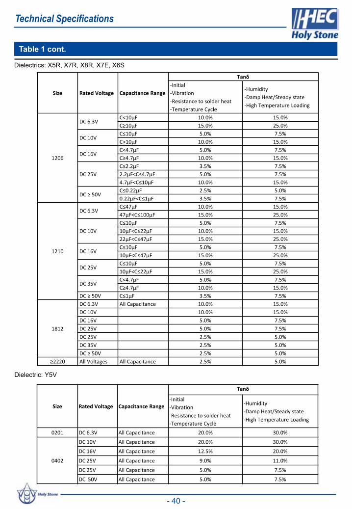
Technical Specifications
Table 1 cont.
- 40 -
Dielectrics: X5R, X7R, X8R, X7E, X6S
Size Rated Voltage Capacitance Range
dĂŶɷ-Initial
-Vibration
-Resistance to solder heat
-Temperature Cycle
-Humidity
-Damp Heat/Steady state
-High Temperature Loading
1206
DC 6.3V�фϭϬђ& 10.0% 15.0%
CшϭϬђ& 15.0% 25.0%
DC 10VCчϭϬђ& 5.0% 7.5%
�хϭϬђ& 10.0% 15.0%
DC 16V�фϰϳђ& 5.0% 7.5%
Cшϰϳђ& 10.0% 15.0%
DC 25V
CчϮϮђ& 3.5% 7.5%
ϮϮђ&ф�чϰϳђ& 5.0% 7.5%
ϰϳђ&ф�чϭϬђ& 10.0% 15.0%
DC ш�ϱϬsCчϬϮϮђ& 2.5% 5.0%
ϬϮϮђ&ф�чϭђ& 3.5% 7.5%
1210
DC 6.3VCчϰϳђ& 10.0% 15.0%
ϰϳђ&ф�чϭϬϬђ& 15.0% 25.0%
DC 10V
CчϭϬђ& 5.0% 7.5%
ϭϬђ&ф�чϮϮђ& 10.0% 15.0%
ϮϮђ&ф�чϰϳђ& 15.0% 25.0%
DC 16VCчϭϬђ& 5.0% 7.5%
ϭϬђ&ф�чϰϳђ& 15.0% 25.0%
DC 25VCчϭϬђ& 5.0% 7.5%
ϭϬђ&ф�чϮϮђ& 15.0% 25.0%
DC 35V�фϰϳђ& 5.0% 7.5%
Cшϰϳђ& 10.0% 15.0%
DC ш�ϱϬs Cчϭђ& 3.5% 7.5%
1812
DC 6.3V All Capacitance 10.0% 15.0%
DC 10V 10.0% 15.0%
DC 16V 5.0% 7.5%
DC 25V 5.0% 7.5%
DC 25V 2.5% 5.0%
DC 35V 2.5% 5.0%
DC ш�ϱϬs 2.5% 5.0%
ш2220 All Voltages All Capacitance 2.5% 5.0%
Size Rated Voltage Capacitance Range
dĂŶɷ
-Initial
-Vibration
-Resistance to solder heat
-Temperature Cycle
-Humidity
-Damp Heat/Steady state
-High Temperature Loading
0201 DC 6.3V All Capacitance 20.0% 30.0%
0402
DC 10V All Capacitance 20.0% 30.0%
DC 16V All Capacitance 12.5% 20.0%
DC 25V All Capacitance ϵϬй 11.0%
DC 25V All Capacitance 5.0% 7.5%
DC 50V All Capacitance 5.0% 7.5%
Dielectric: Y5V
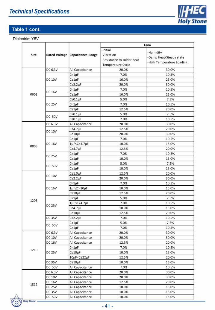
Technical Specifications
Table 1 cont.
- 41 -
Dielectric: Y5V
Size Rated Voltage Capacitance Range
dĂŶɷ-Initial
-Vibration
-Resistance to solder heat
-Temperature Cycle
-Humidity
-Damp Heat/Steady state
-High Temperature Loading
0603
DC 6.3V All Capacitance 20.0% 30.0%
DC 10V
�фϭђ& 7.0% 10.5%
Cшϭђ& 16.0% 25.0%
CшϮϮђ& 20.0% 30.0%
DC 16V�фϭђ& 7.0% 10.5%
Cшϭђ& 16.0% 25.0%
DC 25V
CчϬϭђ& 5.0% 7.5%
�фϭђ& 7.0% 10.5%
Cшϭђ& 12.5% 20.0%
DC 50V�фϬϭђ& 5.0% 7.5%
CшϬϭђ& 7.0% 10.5%
0805
DC 6.3V All Capacitance 20.0% 30.0%
DC 10VCчϰϳђ& 12.5% 20.0%
CшϭϬђ& 20.0% 30.0%
DC 16V
Cшϭђ& 7.0% 10.5%
ϭђ&ч�фϰϳђ& 10.0% 15.0%
Cшϰϳђ& 12.5% 20.0%
DC 25V�фϭђ& 7.0% 10.5%
Cшϭђ& 10.0% 15.0%
DC 50V�фϭђ& 5.0% 7.5%
Cшϭђ& 10.0% 15.0%
1206
DC 10VCчϭϬђ& 12.5% 20.0%
CшϮϮђ& 20.0% 30.0%
DC 16V
�фϭђ& 7.0% 10.5%
ϭђ&ч�фϭϬђ& 10.0% 15.0%
CшϭϬђ& 12.5% 20.0%
DC 25V
�фϭђ& 5.0% 7.5%
ϭђ&ч�фϰϳђ& 7.0% 10.5%
Cшϰϳђ& 10.0% 15.0%
CшϭϬђ& 12.5% 20.0%
DC 35V CчϮϮђ& 7.0% 10.5%
DC 50V�фϭђ& 5.0% 7.5%
Cшϭђ& 7.0% 10.5%
1210
DC 6.3V All Capacitance 20.0% 30.0%
DC 10V All Capacitance 20.0% 30.0%
DC 16V All Capacitance 12.5% 20.0%
DC 25V
�фϭђ& 7.0% 10.5%
CчϭϬђ& 10.0% 15.0%
ϭϬђ&ф�чϮϮђ& 12.5% 20.0%
DC 35V CчϭϬђ& 10.0% 15.0%
DC 50V All Capacitance 7.0% 10.5%
1812
DC 6.3V All Capacitance 20.0% 30.0%
DC 10V All Capacitance 20.0% 30.0%
DC 16V All Capacitance 12.5% 20.0%
DC 25V All Capacitance 10.0% 15.0%
DC 35V All Capacitance 10.0% 15.0%
DC 50V All Capacitance 10.0% 15.0%

Standard packing 10Kpcs/pack. Special customer requirements considered. z Bulk Packing
Paper Tape Embossed Tape
Embossed Carrier Tape
Top Cover Tape
Bottom Cover Tape
Carrier Tape
Top Cover Tape
z Tape Packing
Leader Section20mm min.
Trailer Section40mm min. Chip Section
400mm min.Drawing Direction
NA᧶Not Available
Material And Quantity (¢180mm)
0201 0.6 0.3 Td0.33 15,000 pcs/reel N/A0402 1.0 0.5 Td0.55 10,000 pcs/reel N/A0603 1.6 0.8 Td0.90 4,000 pcs/reel N/A0805 2.0 1.25 Td0.90 4,000 pcs/reel N/A
0.9< Td1.25 N/A 3,000 pcs/reel1206 3.2 1.6 Td0.90 4,000 pcs/reel N/A
0.9< Td1.25 N/A 3,000 pcs/reelT>1.25 N/A 2,000 pcs/reel
1210 3.2 2.5 Td1.25 N/A 3,000 pcs/reel T>1.25 N/A 2,000 pcs/reel
1808 4.6 2.0 Td1.25 N/A 3,000 pcs/reelT>1.25 N/A 2,000 pcs/reel
1812 4.6 3.2 Td2.20 N/A 1,000 pcs/reelT>2.20 N/A 700 pcs/reel
1825 4.6 6.35 Td2.20 N/A 700 pcs/reelT>2.20 N/A 400 pcs/reel
2208 5.7 2.0 Td2.20 N/A 1,000 pcs/reel2211 5.7 2.8 Td2.20 N/A 1,000 pcs/reel
T>2.20 N/A 700 pcs/reel2220 5.7 5.0 Td2.20 N/A 1,000 pcs/reel
T>2.20 N/A 700 pcs/reel2225 5.7 6.35 Td2.20 N/A 700 pcs/reel
T>2.20 N/A 400 pcs/reel
Chip Size Dimension (mm) ¢180mm reel(EIA Code) L W T Paper Tape Plastic Tape
¡ Multilayer Ceramic Chip Capacitor
Packing Information
-42 -

t C D E
HG
FA
B
Pitching Hole I Chip Cavity
z Dimensions of Tape Specification
Paper Tape
0201 0402 0603 0805 1206 1210 A 0.37±0.1 0.61±0.1 1.10±0.2 1.50±0.2 1.90±0.2 2.90±0.2 B 0.67±0.1 1.20±0.1 1.90±0.2 2.30±0.2 3.50±0.2 3.60±0.2 C 4.00±0.1 -- --> D 2.0±0.05 -- --> E 2.00±0.1 -- --> 4.00±0.1 -- --> F 1.75±0.1 -- --> G 3.5±0.05 -- --> H 8.00±0.3 -- --> I ¢1.5+0.1/-0 -- --> t 1.1 max. -- -->
Unit᧶mm
C D E
HG
FA
B
Pitching Hole I Chip Cavity
Ot
J
Embossed Tape
Unit᧶mm 0805 1206 1210 1808 2208 1812 1825 2211 2220 2225
A 1.5±0.1 1.9±0.2 2.9±0.2 2.5±0.2 2.5±0.2 3.6±0.2 6.9±0.2 3.2±0.2 5.4±0.2 6.9±0.2B 2.3±0.2 3.5±0.2 3.6±0.2 4.9±0.2 6.1±0.2 4.9±0.2 4.9±0.2 6.1±0.2 6.1±0.2 6.1±0.2C 4.0±0.1 ÎD 2.0±0.05 ÎE 4.0±0.1 Î 8.0±0.1 ÎF 1.75±0.1 ÎG 3.5±0.05 Î 5.5±0.05 ÎH 8.0±0.3 Î 12.0 +3/-0 ÎI ¢1.5+0.1/-0 ÎJ 3.0 max. Î 4.0 max. Ît 0.3 max. ÎO 0.15 min. Î
Packing Information
- 43 -
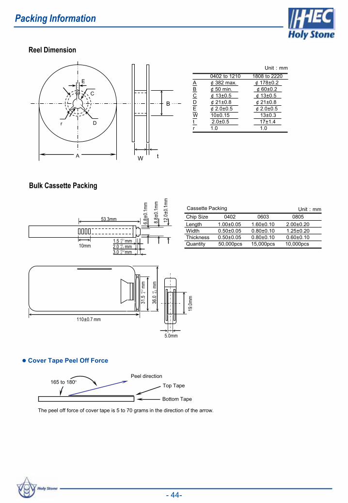
Reel Dimension
r D
E
C
A W t
B
Unit᧶mm 0402 to 1210 1808 to 2220
A ¢ 382 max. ¢ 178±0.2 B ¢ 50 min. ¢ 60±0.2 C ¢ 13±0.5 ¢ 13±0.5 D ¢ 21±0.8 ¢ 21±0.8E ¢ 2.0±0.5 ¢ 2.0±0.5W 10±0.15 13±0.3 t 2.0±0.5 17±1.4 r 1.0 1.0
Bulk Cassette Packing19
.0mm
5.0mm
6.8±0
.1mm
8.8±0
.1mm
12.0±
0.1mm
10mm
53.3mm
1.5 mm +0.1-0
2.0 mm +0-0.1
3.0 mm +0.2-0
36.0
m
m
+0 -0
.2
31.5
m
m
+0
.2-0
110±0.7 mm
165 to 180qTop Tape
Bottom Tape
The peel off force of cover tape is 5 to 70 grams in the direction of the arrow.
z Cover Tape Peel Off Force
Packing Information
Chip Size 0402 0603 0805Cassette Packing
Length 1.00±0.05 1.60±0.10 2.00±0.20 Width 0.50±0.05 0.80±0.10 1.25±0.20 Thickness 0.50±0.05 0.80±0.10 0.60±0.10 Quantity 50,000pcs 15,000pcs 10,000pcs
Unit᧶mm
- 44-
Peel direction

Temperature Coefficient Performance Class EIA Symbol Dielectric Code Temperature Range(Ԩ) Capacitance Change Reference Temperature
ǿ��������������13������������������� N -55Ԩ ~ +125 Ԩ 0±30 ppm/Ԩ 25ԨSL L -25Ԩ ~ +85 Ԩ +350/-1000 ppm/Ԩ 25Ԩ
Ȇ��������������;�5�������������������������������X -55Ԩ ~ +125Ԩ ±15% 25ԨX7E C -55Ԩ ~ +125Ԩ ±4.7% 25ԨX5R B -55Ԩ ~ +85Ԩ ±15% 25ԨY5V Y -30Ԩ ~ +85Ԩ +22/-82% 25ԨY5U E -30Ԩ ~ +85Ԩ +22/-56% 25ԨZ5U Z +10Ԩ ~ +85Ԩ +22/-56% 25Ԩ
¡EIA Designations
Low Temp. Symbol
High Temp. Symbol
Max. %ႤC Symbol
-55Ԩ X-30Ԩ Y+10Ԩ Z
+45Ԩ 3+65Ԩ 4+85Ԩ 5+105Ԩ 6+125Ԩ 7+150 Ԩ 8+200 Ԩ 9
±1.0% A±1.2% B±2.2% C±3.3% D±4.7% E±7.5% F±10.0% P±15.0% R±22.0% S+22% /-33% T+22% /-56% U+22% /-82% V
Ageing RateNP0: 0X7R/X5R : 1 ~ 4 % /decadeY5V : 6~10 % /decade
¡ Dielectric Material – Ageing Rate
After performing de-ageing at 150±5 Ԩ for 30 minutes andplacement at room temperature for 48 hours.
Coefficient of capacitance (ppm/ Ԩ)
Multiplier applicable to column
Tolerance of temp. coeff.(ppm/ Ԩ)
0.0 C1.0 M1.5 P2.2 R3.3 S4.7 T7.5 U
-1.0 0-10 1-100 2-1000 3-10000 4+1 5+10 6+100 7+1000 8+10000 9
30 G60 H120 J250 K500 L1000 M2500 N
For Class Ȇ DielectricsFor Class ǿ�Dielectrics
Ex.: C0G 0±30ppm/ ԨU2J Negative 750±120ppm/ Ԩ
Ex.: X7R -55 ~ +125 Ԩ ±15%Y5V -30 ~ +85 Ԩ +22%/-82%
EIA Designations
- 45 -

Improper circuit layout and pad/land size may cause poor solder joints between the component and thePC board. Insufficient solder may create weak joints and excessive solder may increase the potential ofmechanical or thermal cracks within the ceramic capacitor. Therefore we recommend the solder pad/landsize to be as shown in the following table:1. Size and recommended land dimensions for reflow soldering
EIA CodeChip (mm) Land (mm)
L W A B C D E0201 0.60 0.30 0.2~0.3 0.2~0.4 0.2~0.4 -- --0402 1.00 0.50 0.3~0.5 0.3~0.5 0.4~0.6 -- --0603 1.60 0.80 0.4~0.6 0.6~0.7 0.6~0.8 -- --0805 2.00 1.25 0.7~0.9 0.6~0.8 0.8~1.1 -- --1206 3.20 1.60 2.2~2.4 0.8~0.9 1.0~1.4 1.0~2.0 3.2~3.71210 3.20 2.50 2.2~2.4 1.0~1.2 1.8~2.3 1.0~2.0 4.1~4.61808 4.60 2.00 2.8~3.4 1.8~2.0 1.5~1.8 1.0~2.8 3.6~4.11812 4.60 3.20 2.8~3.4 1.8~2.0 2.3~3.0 1.0~2.8 4.8~5.31825 4.60 6.35 2.8~3.4 1.8~2.0 5.1~5.8 1.0~4.0 7.1~8.32208 5.70 2.00 4.0~4.6 2.0~2.2 1.5~1.8 1.0~4.0 3.6~4.12211 5.70 2.80 4.0~4.6 2.0~2.2 2.0~2.6 1.0~4.0 4.4~4.92220 5.70 5.00 4.0~4.6 2.0~2.2 3.5~4.8 1.0~4.0 6.6~7.12225 5.70 6.35 4.0~4.6 2.0~2.2 5.1~5.8 1.0~4.0 7.1~8.3
2. Mechanical strength varies according to the location of the chip capacitors on the P.C. board.Design the layout of the PCB in such a way as to minimize stress imposed on the components uponflexing the boards during depanelization or other processes.
Component layout close to the edge of the board or the“depanelization line” is not recommended. Susceptibilityto stress is in the order of: a>b>c and d>e
a
cb
d
slitperforatione
In the pick and place operation, if the low dead point is too low, excessive stress is applied tocomponent. This may cause cracks in the ceramic capacitor, it is therefore recommended to move thelow dead point of the nozzle to a higher level to minimize board warpage and stress on the components.Nozzle pressure should be adjusted to 1N to 3N (static load) during the pick and place operation.
1. Sometimes cracking can be caused by the impact load of the pick and place nozzle.
Nozzle
Crack
Excessive Stress Warping of Board
PCB
Warping of Board
Support pin
2. Amount of Adhesive a a
b
c c
Example : 0805 & 1206
¡ Construction of Board Pattern
¡ Mounting
E
Land
A
Solder Resistor
C
B
Capacitor
D
Slit
Precautionary Information
a 0.2mm min.b ���a�����ȝPc Do not touch the solder land
- 46 -

¡ Handling after chip mounting
1. Proper handling of the PCB is recommended since excessive bending and twisting of the PCB may induce mechanical stress and cause internal cracking of the capacitor.
2. There is a potential of cracking if the board is warped due to excessive load from the check pin.
Check pinCheck pin
Support Pin
3. Examples of PCB de-panelization jigs:
High potential of cracking Low potential of cracking
Bending
Twist
Bad
V-groove
PCB splitting jig
PCB
The outline of a PCB breaking jig is shown below. It is recommended when dividing or breaking PCBsthat they are held near the jig where no bending will occur. In this way there will be no compressivestress applied to the components or capacitors on the PCB. Do not hold the PCB at a position which isfar away from the jig. Tensile stress may cause the capacitors to crack.
Poor Dividing Load DirectionLoad Direction
PCB
V-groove
Chip Component
Recommend Dividing
Load Direction
Load Direction
Chip Component
Precautionary Information
- 47 -
Good

1. Wave Soldering
Recommended wave soldering profile
¡Soldering
Most components are wave soldered with solder at 230 to 250°C. Adequate care must be taken toprevent the potential of thermal cracks in the ceramic capacitors. Refer to the soldering methods belowfor optimum soldering benefits. For SMC range see special recommendations on page 34.
Soldering Method Change in Temp.(Ԩ)1206 and Under 'T d100~130Ԩmax.
1210 to 1812 'T d70~100Ԩmax2220 and greater Not recommended
To optimize the result of soldering, proper preheating is essential:1) Preheat temperature is too low
a. Flux flows too easilyb. Possibility of thermal cracks
2) Preheat temperature is too higha. Flux deteriorates even when oxide film is removedb. Causes warping of the circuit boardc. Loss of reliability in chips and other components
2. Reflow SolderingPreheating to the reflow temperature is recommended to decrease the potential of thermal cracking inthe components. The recommended heating rate depends on the size of component, however it shouldnot exceed 3°C/Sec.Recommend reflow profile for lead-free soldering temperature profile (MIL-STD-202G #210F)
Soldering Method Change in Temp.(Ԩ)1206 and Under 'T d190Ԩ1210 and Over 'T d130Ԩ
Cooling Condition:Natural cooling using air is recommended. Forced cooling should be avoided. However if the chips aredipped into a solvent for cleaning, the temperature difference (ǻT ) between the solvent and the chipsmust be less than 100°C.
Tem
pera
ture
(qC
)
217
260max.
150°C /60sec. Min. 70 to 90 sec.
Pre-heating SolderingCooling
'T
260 °C max./ 10 sec.
120seconds or more2 to 3 sec.
60seconds or more
'T
Tem
pera
ture
(qC
)
200
250
300
Pre-heatingSoldering
Cooling
230
Number of soldering cycles : 2 (max.)
Precautionary Information
- 48 -
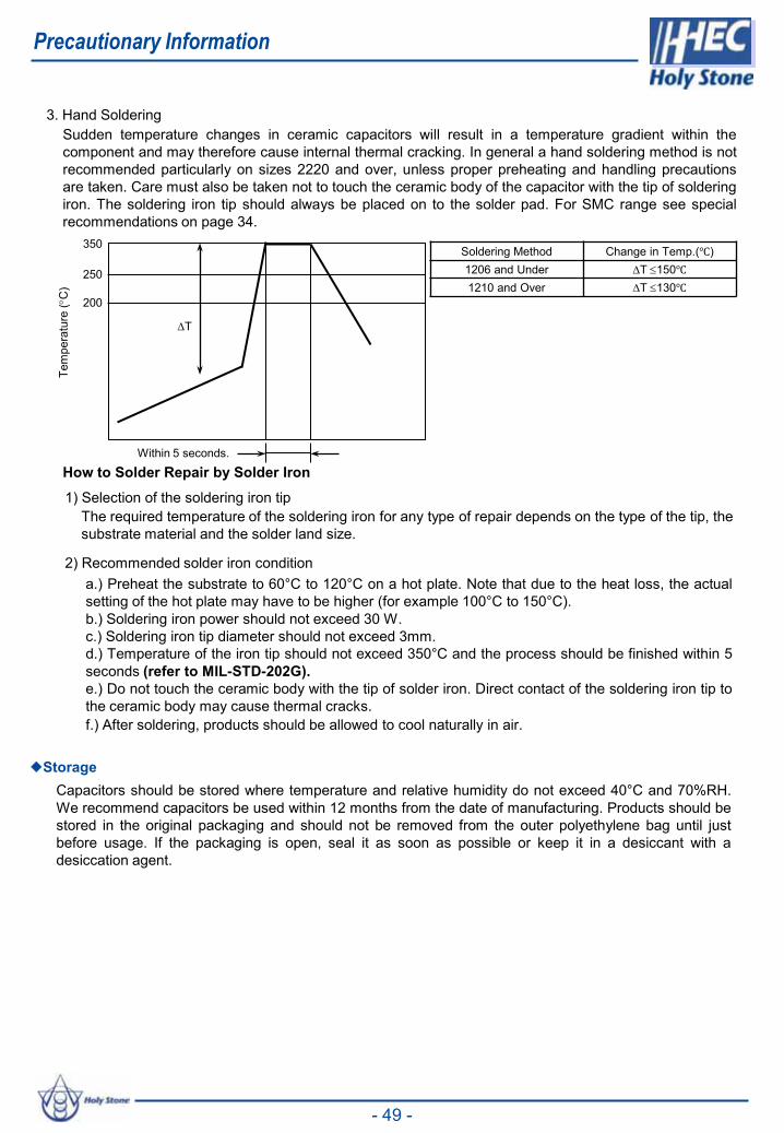
How to Solder Repair by Solder Iron
1) Selection of the soldering iron tip The required temperature of the soldering iron for any type of repair depends on the type of the tip, the substrate material and the solder land size.
2) Recommended solder iron condition a.) Preheat the substrate to 60°C to 120°C on a hot plate. Note that due to the heat loss, the actualsetting of the hot plate may have to be higher (for example 100°C to 150°C).b.) Soldering iron power should not exceed 30 W.c.) Soldering iron tip diameter should not exceed 3mm.d.) Temperature of the iron tip should not exceed 350°C and the process should be finished within 5seconds (refer to MIL-STD-202G).e.) Do not touch the ceramic body with the tip of solder iron. Direct contact of the soldering iron tip tothe ceramic body may cause thermal cracks.f.) After soldering, products should be allowed to cool naturally in air.
Capacitors should be stored where temperature and relative humidity do not exceed 40°C and 70%RH.We recommend capacitors be used within 12 months from the date of manufacturing. Products should bestored in the original packaging and should not be removed from the outer polyethylene bag until justbefore usage. If the packaging is open, seal it as soon as possible or keep it in a desiccant with adesiccation agent.
3. Hand SolderingSudden temperature changes in ceramic capacitors will result in a temperature gradient within thecomponent and may therefore cause internal thermal cracking. In general a hand soldering method is notrecommended particularly on sizes 2220 and over, unless proper preheating and handling precautionsare taken. Care must also be taken not to touch the ceramic body of the capacitor with the tip of solderingiron. The soldering iron tip should always be placed on to the solder pad. For SMC range see specialrecommendations on page 34.
Soldering Method Change in Temp.(Ԩ)1206 and Under 'T d150Ԩ1210 and Over 'T d130Ԩ
'T
Tem
pera
ture
(qC
)
200
250
350
Within 5 seconds.
¡Storage
Precautionary Information
- 49 -
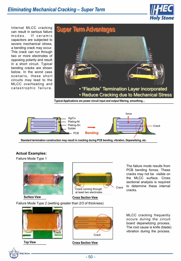
Internal MLCC crackingcan result in serious failurem o d e s . I f c e r a m i ccapacitors are subjected tosevere mechanical stress,a bending crack may occur.This crack can run throughtwo or more electrodes ofopposing polarity and resultin a short circuit. Typicalbending cracks are shownbelow. In the worst casescenar io , t hese shor tcircuits may lead to theMLCC overheating andc a t a s t r o p h i c f a i l u r e .
Bending
Ag/Cu
Plating-SnPlating-Ni
PCB
Solder
force
Crack
Typical Applications are power circuit input and output filtering, smoothing…
Standard termination construction may result in cracking during PCB bending, vibration, Depanelizing, etc.
CrackCrack running through at least two electrodes.
Surface View Cross Section View
Actual Examples:Failure Mode Type 1
The failure mode results fromPCB bending forces. Thesecracks may not be visible onthe MLCC surface. Crosssectional analysis is requiredto determine these internalcracks.
Failure Mode Type 2 (wetting greater than 2/3 of thickness)
Top View Cross Section View
MLCC cracking frequentlyoccurs during the circuitboard depanelizing process.The root cause is knife (blade)vibration during the process.
CrackCrack
Eliminating Mechanical Cracking – Super Term
- 50 -
Super Term Advantages
• “Flexible” Termination Layer incorporated• Reduce Cracking due to Mechanical Stress
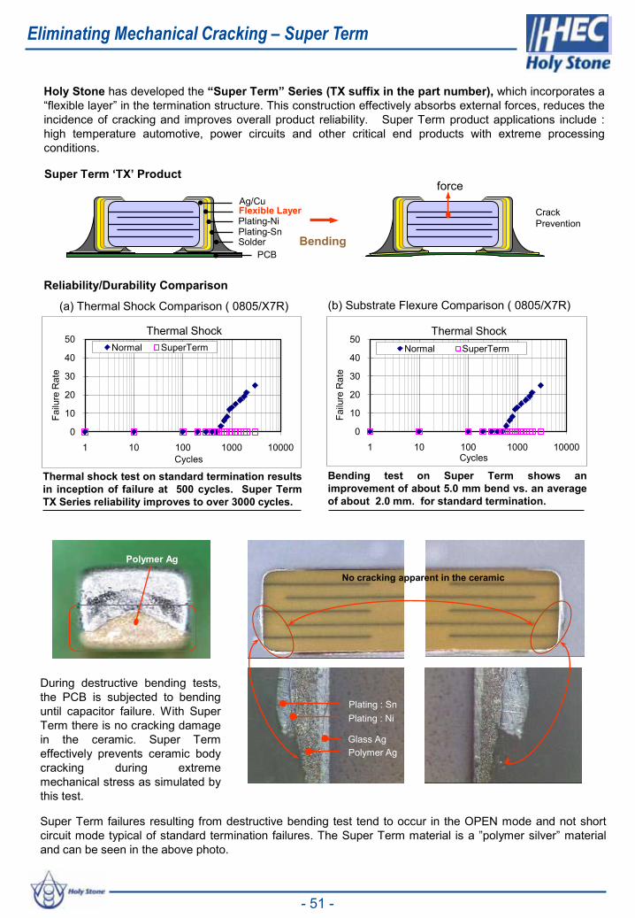
Bending test on Super Term shows animprovement of about 5.0 mm bend vs. an averageof about 2.0 mm. for standard termination.
Thermal shock test on standard termination resultsin inception of failure at 500 cycles. Super TermTX Series reliability improves to over 3000 cycles.
Holy Stone has developed the “Super Term” Series (TX suffix in the part number), which incorporates a“flexible layer” in the termination structure. This construction effectively absorbs external forces, reduces theincidence of cracking and improves overall product reliability. Super Term product applications include :high temperature automotive, power circuits and other critical end products with extreme processingconditions.
Bending
Ag/Cu
Plating-SnPlating-Ni
PCBSolder
Flexible Layer
force
Crack Prevention
Super Term ‘TX’ Product
(a) Thermal Shock Comparison ( 0805/X7R)
Reliability/Durability Comparison (b) Substrate Flexure Comparison ( 0805/X7R)
Plating : SnPlating : Ni
Polymer AgGlass Ag
During destructive bending tests,the PCB is subjected to bendinguntil capacitor failure. With SuperTerm there is no cracking damagein the ceramic. Super Termeffectively prevents ceramic bodycracking during extrememechanical stress as simulated bythis test.
No cracking apparent in the ceramic
Super Term failures resulting from destructive bending test tend to occur in the OPEN mode and not shortcircuit mode typical of standard termination failures. The Super Term material is a ”polymer silver” materialand can be seen in the above photo.
Polymer Ag
Eliminating Mechanical Cracking – Super Term
- 51 -
0
10
20
30
40
50
1 10 100 1000 10000
Failu
re R
ate
Cycles
Thermal ShockNormal SuperTerm
0
10
20
30
40
50
1 10 100 1000 10000
Failu
re R
ate
Cycles
Thermal ShockNormal SuperTerm

Holy Stone has developed an Arc Preventioncoating process that coats the surface of thedielectric without encroaching onto thetermination material. This coating makes thesurface of the dielectric non porous and preventsmoisture and dirt becoming trapped thusreducing the surface resistance and the arcingvoltage of the capacitor. It has been shown thatthe arcing voltage can be increased by up to65% on soldered parts by using the Holy StoneArc Prevention Coating.
MLCC Arc Prevention – for Hi-Pot Testing
Typical Applications for telecommunication devices(IEEE802.3) in LAN interface, Ballast…
Due to the open and porous natureof the surface of the X7R dielectric,moisture and/or dirt which will havea lower resistance than thedielectric grains, can becomeentrapped in the surface. Dirt canalso include any flux residues as aresult of the soldering process. Thisdirt/flux as well as becomingentrapped into the surface will, initself, attract additional moistureonto the surface thus reducing thesurface resistance and the voltageat which arcing occurs. Surfacearcing or flashover at worst cancause equipment failure duringisolation testing and, in addition, willleave a carbon track on the surfacewhich can lead to eventual failure ofthe capacitor.
Typical surface arcing on X7R MLCC is from termination-to-termination (shown in polarized light)
NP0 & X7R Material Characteristic Comparison
Item NP0 X7RDielectric Constant 30 ~ 100 2000 ~ 4000
I. Resistance >1013 : >1011 :
B.D. Voltage 70~80 Vdc/um 40~50 Vdc/umGrain Size < 500nm 900nm ~ 1500nm
Grain Size(x8000)
Porosity (x1000)
• The different grain shape and size willlead to different grain density aftersintering.
• The grain size of NP0 dielectric issmaller than that of X7R resulting adenser and less porous structure.
• Surface porosity will trap dirt, flux andm o i s t u r e c a u s i n g t h e s u r f a c eresistance to dramatically decrease.
• Low surface resistance will cause thearcing voltage to reduce, possiblyleading to failure of the capacitor orequipment during isolation testing.
• Using the Holy Stone Arc Preventioncoating effectively makes the surface ofX7R dielectric similar to that of NP0.
Arc Prevention
Passed IEEE 802.3 1500VAC or 2250VDC
Increases voltage at which arcing occurrs
Coated Products for Surface Arc Prevention
- 52 -

3.2mmSolder Ball
Solder balls reduce the creepage distance between terminations and thus reduce the arcing voltage
Creepage distance v.s. Arcing Voltage Recommended Solder Pad Design
Land
A
Solder Dam
C
B
Capacitor
EIA Code Chip (mm) Land (mm)L W A B C
1808 4.6±0.3 2.0 ±0.2 3.2~3.6 1.2~2.4 1.5~1.81812 4.6±0.3 3.2 ±0.2 3.2~3.6 1.2~2.4 2.3~3.02208 5.7±0.4 2.0 ±0.2 4.0~4.6 1.2~2.4 1.5~1.82211 5.7±0.4 2.0 ±0.3 4.0~4.6 1.2~2.4 2.0~2.62220 5.7±0.4 5.0 ±0.4 4.0~4.6 1.2~2.4 3.5~4.8
Distance between terminations also has a direct effect on the arcing voltage. The greater the distance (chipsize) the higher this voltage will be. Solder pad design will have a significant effect on the arcing of highvoltage capacitors. Above is our recommended solder pad land design or each chip size.
Arc Prevention Coating. The application of the Arc Prevention coating, which is a high insulation resistance material, coats the surfaceof the dielectric with a smooth and non porous layer that prevents moisture entering the surface pours and alsoaids cleaning post soldering. The following diagrams show the difference between coated and non coated X7Rcomponents.
Item Porosity (x1000)Before
After
Surface Appearance of non coated and coated product.
Surface Comparison High Voltage Test Comparison
• The coating reduces the porosity of the X7R surface and provides a smooth surface which help prevent surface arcing.• The maximum Hi-pot test level may be increased by >1000Vdc after coating with both unsoldered and soldered components.
Using the Holy Stone Arc Prevention coating increases the surface arcing voltage of X7R capacitors toalmost that of an equivalent NP0 part, however the higher dielectric constant of X7R allows for highercapacitance values to be achieved in any given case size. The Holy Stone Arc Prevention coating providesa total solution to the harmful effects of surface arcing.
High Voltage Test
0
10
20
30
40
50
60
70
100 1000 10000Voltage (Vdc)
Failu
re R
ate
(%) Normal Type
Coated Product
- 53 -
Coated Products for Surface Arc Prevention

MLCC , Ceramic Disc Capacitors: NP0, SL, X7R, X5R, X6S, X7E, Y5V and Y5U dielectrics.z Description:
z Basic Construction/Homogenous Material :(a) Standard Type (b) “X” Type: Super Termination (Option)
External Electrodes
Barrier
Solder Metal
Inner Electrodes
Polymer ElectrodesExternal ElectrodesBarrier
Solder Metal
Inner Electrodes
Ceramic Body Ceramic Body
Multi-layer Ceramic Chip capacitors are homogenous devices manufactured from materials that cannot be mechanically disjointed into different materials.Multi-layer Ceramic Chip products : Standard sizes are fully RoHS compliant.
Group Series RoHS Status
Cadmium HexavalentChromium
Lead * Mercury PBBs PBDE
Limit <0.01% <0.01% <0.1% <0.01% <0.01% 0.01%
MLC FamilySurface MountProducts
NCC,HCC,VAC,RFC, HCX, SMC, LCC
Available � � � � � �
TCX,LDC, HTC Available � � � � � �
HCN,SACSCC,
Available � � � / � * � � �
HVC NP0 Available � � � / �* � � �
X7R Available � � � / � * � � �
* Pb in internal ceramic insert – exempt from RoHS annex 7 to Article 4.1
RoHS Status Lead-Free Status / MSL level
External plating : 100% Matte Sn as standard. Pb-free reflow & wave solder compliant, MSL=1Reflow : 260Ԩ max recommended.Wave : 260Ԩ max recommended,
Wave & reflow profile refer to HEC recommended solder profile.
Part Number Designation: RoHS compliant : No change to P/N(Generally no change to P/N, but available Pb-free : No change to P/Nas P/N prefix at customer request)
Product marking : Pb free : Pb free(available at customer request, highlighted ormarked on reel and container) refer to JEDEC&IPC Std.
-54 -
RoHS Compliant

ISO Certifications
Plant Certificated Date Organization Registration No.
Taipei HQ/Lung Tan Factory ISO 9001:2000 20,Mar.,2002 BVQI TW08098Q
Taipei HQ/Lung Tan Factory ISO 14001:1996 29,May,2003 BVQI 131145
Dongguan Manufacturing ISO 9001:2000 16.Dec.,2003 BVQI TW08098Q
Taipei HQ/Lung Tan Factory QS 9000 : 1998 04.Oct.,2004 BVQI 162522
ISO 14001:1996ISO 9001:2000 QS 9000:2004
- 55 -
ISO Certifications
- 56 -
MEMO

Wor
ldwi
de S
ales C
onta
cts
Edition 2010.10
䱍⇇⪑←㯼匰㦘棟⏻⚇Holy Stone Enterprise Co., Ltd.
A Partner You Can Trust
• Lungtan Plant / 爜䇼䞮䞱ℚ㯼壤㫒⦡傲爜䇼掘䍞㨦㧠ぴ℣恾90ゆ56壮No.56, Lane 90, Kung Wu Road, Wu Lin Village, Lung Tan Hsiang, Tao Yuan County, Taiwan, R.O.C. Tel: 886-3-4995288Fax: 886-3-4995299 Zip code: 325
• Taipei HQ / ♿▦僌⏻⚇♿▦ゑ⏶䃥●䜿⼀恾ℛ㹄62壮1㲢
1FL, No. 62, Sec. 2, Huang Shan Rd., Nei Hu Dist., Taipei, Taiwan, R.O.C. Tel: 886-2-26270383Fax: 886-2-27987181 Zip code: 114
• Kaohsiung Sales Office / 浧楓⒕⏻⚇浧楓ゑⓜ昽●㉒恾239壮8㲢8FL-1, No.239, Yi-Hsin 1st. Road, Chien Chen Dist., Kaohsiung, Taiwan, R.O.C. Tel: 886-7-5366115Fax: 886-7- 5366105 Zip code: 806
• Suzhou Sales Office / 墖ね⒕⏻⚇墖ねゑ㠿●掶⺘恾9壮䇳㘆ㅲ⫃ 1㭮208⸳Room 208, Building 1 Runjie Plaza, No.9 Dengwel Road, Suzhou New Area, ChinaTel: 86-512-82100058 Fax: 86-512-68026968 Zip code: 215021
• Dongguan Plant / 㨀嘭ㅯㅲ㨀䦐㨀嘭ゑ⫧ㅗ昽奮⫧㧠⺅䪂ぴ㯼●Baoshi Industrial Area, Jiaoyitang Tangxia Town, Dongguan Guangdong, China.Tel: 86-769-87928002Fax: 86-769-87914761 Zip code: 523723
• Shanghai Sales Office / ₙ䀆⒕⏻⚇ₙ䀆ゑㆅ⸘導恾1160⚆氥≰枅掌⮶☵16㰋16F, Shouxinyindu Building, 1160 YanAn (W) Road, Shanghai, China.Tel: 86-21-51875266Fax: 86-21-62826722 Zip Code: 200052
Location in Taiwan
Location in China
Location in USA• Holy Stone International
26395 Jefferson Ave. Suite H Murrieta, CA, 92562, USATel : 951-696-4300Fax: 951-696-4301 Website: http//www.holystonecaps.comEmail: [email protected]
• Hong Kong Office / 氨䂾⒕⏻⚇氨䂾爜䋲⸞栚拢15壮爜䋲ぴ㯼₼㉒726⸳Room 726, Kowloon Bay Industrial Center , 15 Wang Hoi Road, Kowloon Bay, Hong Kong.Tel: 852-23055141Fax: 852-23055789
Location in Europe• Holy Stone (Europe) Ltd.
Henderson Business Centre, Unit 24, Ivy Road, Norwich, Norfolk, NR5 8BF, United KingdomTel: +44 (0)1603 251780Fax: +44 (0)1603 251786Website: http//www.holystonecaps.comEmail: [email protected]
Location in Singapore
Blk 7 Kallang Place #03-04 ,Singapore 339153Tel : (65) 6513 2343Fax: (65)6563 6705
• Holy Stone Holdings Co., Ltd.