center for microtechnologies - tu chemnitz
TRANSCRIPT

FACULTY OF ELECTRICAL ENGINEERING AND INFORMATION TECHNOLOGY
I n f o r m a t i o n o n l i n e : w w w . z f m . t u - c h e m n i t z . d e
A N N U A L R E P O R T 2 0 0 7
CHEMNITZ UNIVERSITY OF TECHNOLOGY
CENTER FOR MICROTECHNOLOGIES

Dear ladies and gentlemen,
The year 2007 was a very successful year. As in preceding years, the Center for Microtechnologies in close coop-eration with the Branch Chemnitz of the Fraunhofer Institute for Microintegration and Reliability (Fraunhofer IZM, headquarter Berlin) has further consolidated its position as a Center of Excellence in the fields of micro- and nano-electronics back end technologies and micro- and nanosystem technologies.
The key to our success was an interdisciplinary cooperation of several chairs within the ZfM. Based on this idea, ZfM’s primary mission is to provide an intellectual and working environment that makes possible student educa-tion and research in areas that require or may benefit from advanced ULSI-interconnect technologies, Si-nano-technology and new developments and ideas in the field of MEMS/NEMS by using microfabrication technologies. ZfM’s technology laboratories provide a complex of modern microelectronics laboratories, clean rooms and mi-crofabrication facilities.
We are very pleased that Prof. Dr. Jan Mehner and Prof. Dr. John-Thomas Horstmann were elected as new members of the board of directors of the ZfM in 2007. Prof. Jan Mehner has replaced Prof. Wolfram Dötzel, who retired 2007. Prof. John-Thomas Horstmann has replaced Prof. Gunter Ebest, who also retired 2007. We would like to thank Prof. Wolfram Dötzel and Prof. Gunter Ebest for their long term contribution within the ZfM, especially for their very suc-cessful participation in the Collaborative Research Center “Arrays of micromechanical sensors and actuators”.
We spent a lot of effort in the year 2007 regarding the organisation and design of the Smart Systems Campus Chem-nitz nearby our already existing buildings. Starting in the year 2006 the construction of new buildings for
cleanroom facilities of the ZfM together with the Institute of Physics of the TU Chemnitz•the Branch Chemnitz of the Fraunhofer IZM•facilities for start up companies•
is carried out. The new clean room of the Center for Microtechnologies within the building of the Institute of Phys-ics was finished in 2007.
The 2007 Annual Report of the Center for Microtechnologies provides an overview of the facilities, staff, facul-ty and students associated with the ZfM, as well as a description of many of the ongoing research projects which make use of the ZfM facilities.
These developments, which are based on close links with industry and cooperation with German as well as inter-national institutes, contribute to an advanced education for our students. We kindly acknowledge the support of the Federal Ministry of Research, the German Research Foundation, the Saxon Ministry of Science and the Euro-pean Commission.
As always, we are driven by our triple aims of excellence in education, scientific and technological research and by providing a comprehensive range of research and development ser-vices to industry.
Thomas GessnerPresident of the Center for MicrotechnologiesDirector of Chemnitz Branch of Fraunhofer IZM
Chairman’s letter


Chairman’s letter 1
Contents 3
Center for Microtechnologies 5
Highlights 7
Organization 8
Chairs 9
Co-operations 15
Networks 21
Equipment and service offer 23
Research activities 25
Research projects 27
Special reports
MEMS applications 33
micro and nano electronics 50
design 62
technologies 71
characterization and tests 96
Education 105
Lectures 107
Diploma theses and PhDs 109
Student exchange 111
Public relations and marketing 115
Memberships 117
Scientific publications 118
Trade fairs and events 126
International guests 129
Contents


Center for Microtechnologies
Highlights
Organization
Chairs
Co-operations
Networks
Equipment and service offer


New clean room (clean room class 10) in the new building of Fig.2:
the Institute for Physics
Prof. Dr. Dieter Tischendorf, Fig.1:
Prof. Dr. Thomas Gessner,
and Prof. Dr. Dietrich Zahn at
ceremonial kick-off presentation
of Smart Systems Campus
Chemnitz
Highlights in the year 2007
The year 2007 startet with the final presentation of the Collaborative Research Center (SFB) No. 379 : „Arrays of micromechanical sensors and actuators“. This SFB dealt with the realization of sensor and actuator arrays consisting of a number of single components. New technologies among them the AIM technology have been developed. The final results have been demonstrated to partners from industry and research during the fair SIT on March 1st 2007 in Chemnitz.
In early June the deputy di-rector of the Chinese Acad-emy of Sciences, Prof. Yu De Yu, conferred the title of visiting professor at the Institute of Semiconductors on Prof. Thomas Gessner to acknowledge his outstand-ing contribution to micro and nano technology as well as system integration. With about 1000 employees the Institute of Semiconductors at the Chinese Academy of Sciences in Beijing is one of China’s biggest research in-stitutions.
On July 9th 2007 the ceremonial kick-off presenta-tion of the Smart Systems Campus Chemnitz at the Chemnitz University of Technology took place. The Smart Systems Campus provides a pool of microsystems technology expertise in a dynamic network in Chem-nitz. The park provides a home for renowned scientific and technical institutes and links them to a pioneering spirit, entrepreneurship and an economic upswing right on the doorstep. The Center for Microtechnologies as well as the branch Chemnitz of the Fraunhofer Insti-tute for Reliability and Microintegration belong to this campus. The Center for Microtechnologies got a new clean room within this campus, which was finished in December 2007.
Since November 2007 Prof. Thomas Gessner works as a Principal Investigator in the World Premier International Research Center of the Tohoku University Sendai. The
main objective of the center is to promote the develop-ment of new materials under world-leading organization for interdisciplinary research in functional materials, by use of an innovative method of atom and molecular con-trol, departing from the typical approaches and moving towards the next generation. The center will pursue the creation of new compounds and materials with innova-
tive functions with exceed the existing ones, the con-struction of devices based on a new fundamental par-adigm and the promotion of applied research projects on
materials and system architecture that will generate di-rect social impacts. Main task of the common research are system integration issues of advanced materials and technologies.
In December 2007 the new clean room (clean room class 10) has been finished.
Highlights 7

The Center for Microtechnologies (ZfM) founded in 1991, belongs to the department of Electrical Engi-neering and Information Technology of the Chemnitz University of Technology. It is the basis for education, research and developments in the fields of micro and nano electronics, micro mechanics and microsystem technologies in close cooperation with various chairs of different TUC departments.
The ZfM’s predecessor was the “Technikum Mik-roelektronik” which was established in 1979 as a link between university research and industrie. For that reason the Chemnitz University of Technology has had a tradition and experience for more than 30 years in the fields of microsystem technology, micro and nanoelectronics, as well as opto-electronics and integrated optics.
Within 2007 two professors left the Center for Mi-crotechnologies. At this place we want to thank again
Prof. Wolfram Dötzel and Prof. Gunter Ebest for their scientific work, their commitment and their support. The work will be continued based on the traditions but with new ideas by the new professors Prof. Jan Mehner and Prof. John-Thomas Horstmann.
The ZfM carries out basic research, practical joint projects and direct research & development orders for the industry in the following fields:
Basic technologies and components for mi-•crosystems and nanosystems (sensors, ac-tuators, arrays, back end of line)Design of components and systems•Nanotechnologies, nanocomponents and ul-•trathin functional layers
In education, the specified and related topics are taught in the basic and main courses.
Visit our homepage: http://www.zfm.tu-chemnitz.de
Center for Microtechnologies
8 Organization
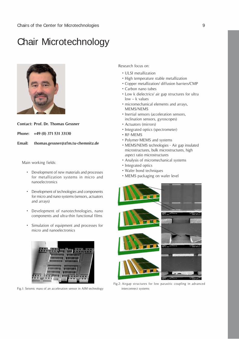
Seismic mass of an acceleration sensor in AIM technologyFig.1:
Airgap structures for low parasitic coupling in advanced Fig.2:
interconnect systems
Contact: Prof. Dr. Thomas Gessner
Phone: +49 (0) 371 531 33130
Email: [email protected]
Chair Microtechnology
Main working fields:
Development of new materials and processes •for metallization systems in micro and nanoelectronics
Development of technologies and components •for micro and nano systems (sensors, actuators and arrays)
Development of nanotechnologies, nano •components and ultra-thin functional films
Simulation of equipment and processes for •micro and nanoelectronics
Research focus on:
ULSI metallization •High temperature stable metallization•Copper metallization/ diffusion barriers/CMP•Carbon nano tubes•Low k dielectrics/ air gap structures for ultra •low – k valuesmicromechanical elements and arrays, •MEMS/NEMSInertial sensors (acceleration sensors, •inclination sensors, gyroscopes)Actuators (mirrors)•Integrated optics (spectrometer)•RF-MEMS•Polymer-MEMS and systems•MEMS/NEMS technologies - Air gap insulated •microstructures, bulk microstructures, high aspect ratio microstructuresAnalysis of micromechanical systems•Integrated optics•Wafer bond techniques •MEMS packaging on wafer level•
Chairs of the Center for Microtechnologies 9

Wireless sensor node developed for MEMSFAB GmbHFig.2:
Step gear system for micro positioning applicationsFig.1:
Contact: Prof. Dr. Jan Mehner
Phone: +49 (0)371 531 36652
E-Mail: [email protected]
The professorship is focused on design and experimental characterization of Microsystems and their applications in precision engineering. Innovative technologies are investigat-ed in order to link mechanics, optics, electrical engineering and electronics for highly integrated smart products.
Research topics are:
Modeling and simulation of physical domains •and their interactions
Experimental characterization and measurement •methodologies
Sensor and actuator development•
Wireless communication and energy •scavenging
Microsystems are key components of complex •heterogeneous devices such as automotives products, industrial automation and consumer applications
Academic research and education is strongly •related to partners as industrial enterprises, Fraunhofer Institutes, software companies
Examples are
Accelerometers and gyroscopes •
Micro mirrors for image projection•
Vibration sensor for process control •
Sensor networks and communication•
Flow rate sensors and vacuum gauges•
Components for medical applications•
The effects of Microsystems technology on intelligence, reliability, energy consumption, volume, mass and costs of market products will be dramatic, similar to the re-placement of electronics based on discrete components by microelectronics in the early 1970s.
Chair Microsystems and Precision Engineering
10 Chairs of the Center for Microtechnologies
Contact: Prof. Dr.-Ing. Ulrich Heinkel
Phone: +49 (0)371 531 24310
E-Mail: [email protected]
Main working fields:
design of ASICs (Application Specific •Integrated Circuits) and FPGAs (Field Programmable Gate Arrays)
design of heterogeneous systems (MEMS) •
design support and optimization by means •of novel approaches, methodologies and dedicated design tools
component (hardware and software) reuse •
high performance arithmetic •
digital image processing •
formal specifications capturing for analogue, •digital and heterogeneous systems with VHDL, VHDL-AMS, SystemC, SystemC-AMS
reconfigurable computing •
During many years of work in the area of circuit and system design, an extensive knowledge in application spe-cific integrated circuits (ASIC) design has been accumu-lated. Special know-how and experience exist in the field of PLD and FPGA (field programmable gate arrays) de-sign and application. Many different systems have been designed, e.g. for real time processing, rapid prototyping systems for image processing, vibration pattern recognition systems and coupling of simulators and emulators.
Research areas include:
system design of heterogeneous microsystems •in co-operation with the Chair of Microsystems and Precision Engineering and the Center of Microtechnologies,
research work in logic and system design and •application of FPGAs and PLDs,
high performance arithmetic for different •special purposes (e.g. MPEG video decoders, image compression, graphic controllers),
design of re-usable components and IP •(Intellectual Properties), development of design environments for re-usable components and applications,
specification capturing, formal specification •with interface-based design methods,
utilisation of fuzzy accelerators for recognition •of vibration patterns and classification (noise analysis),
development and application of a modular •system (including graphical user interface) for real time functions (inspection of textile surfaces, analysis of skin diseases, real time image processing, fuzzy classification systems, controlling of projection systems),
design and evaluation of high performance •data path components,
Low Power Design (system bus encoding •techniques for reduced power dissipation)
Chair Circuit and System Design Chair
Chairs of the Center for Microtechnologies 11

Contact: Prof. Dr. John-Thomas Horstmann
Phone: +49 (0)371 531 37114
E-Mail: [email protected]
Electronic Devices of Micro and Nano Technique
Main working fields:
Manufacturing, analysis •and charac terization of next-generat ion nanoelec tronic devices
in t eg ra t ed c i r cu i t •design for micro system electronics
modelling and simulation of electronic devices •for microsystem electronics
Main research to pics of the “next-generation nano-electronic devices” group at the Chair of Electronic De-vices of Micro and Nano Technique are:
fabrication and experimental characteri zation •of sub-50 nm-MOS-transistors
development of strategies to reduce the •statistical parameter fluctuations of very small MOS-transistors
invention of new materials in the CMOS-•process for next generation nano-devices
Main topics in the research activities of the “mi-crosystem electronics” working group at the Chair of Electronic Devices of Micro and Nano Technique are the development of integrated microsystem front end electronics
The field of activity comprises:
design of integrated high voltage circuits for •electrostatically driven micro actuators
characterisation and modelling of high voltage •micro technology devices
design of low power and low noise integrated •circuits for signal editing of micro-mechanical sensor arrays, and
electrical characterisation of microsystems.•
Competence in integrated circuit design of the working group starts from linear am-plifier circuits with an electrical strength of several hundreds of volts up to low volt-age signal processing circuits in switched-capacitor technique.
Electrostatic driven micromechanical com-ponents with capacitive behaviour referring to their ter minals include micro mirrors rotating in one or two dimen sions and transducers based on the piezoelectric ef-fect. Front-end circuits which are used to con-trol such microelements for various applications have to be smart power amplifiers with the abil-ity to drive up to 1000 V. Various examples of such circuits have been demonstrated over the last years.
12 Chairs of the Center for Microtechnologies

Contact: Prof. Dr. rer. nat. Christian Radehaus
Phone: +49 (0)371 531 33085
E-Mail: [email protected]
Main working fields:
First principle simulation of electronic, optical and mechanical properties of solids
Determination of bulk and interface structures, •Classical Monte Carlo (CMC) and Classical Molecular Dynamics (CMD)
Calculation of electronic band structures •-including GW methods- and dielectric constants
Modeling thermal stability using classical •and ab initio molecular dynamics
Electronic structure of crystalline and •amorphous SiOxNy materials
Si-Insulator Interfaces •
Simulation of defects and their influence •
Developing of new transport models for the •leakage current in CMOS structures
Quantum mechanical simulation of electronic devices
computation of gate tunneling current in •MOSFETs with single and multilayer gate stacks
Interaction of molecules with solid state surfaces
cleaning und sticking problems of various •substances on surfaces
Chair Opto and Solid State Electronics
Chairs of the Center for Microtechnologies 13
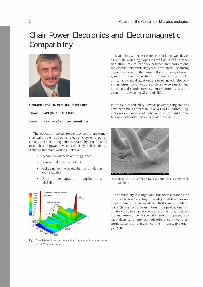
Bond wire lift-off at an IGBT-die after 18000 cycles with Fig.2:
Tj 100K
Simulation of current tubes at strong dynamic avalanche in Fig.1:
a 3.3kV power diode.
Contact: Prof. Dr. Prof. h.c. Josef Lutz
Phone: +49 (0)371 531 33618
Email: [email protected]
The education covers power devices, thermo-me-chanical problems of power electronic systems, power circuits and electromagnetic compatibility. The focus of research is on power devices, especially their reliability. Actually the main working fields are
Dynamic avalanche and ruggedness•
Diamond like carbon a-C:H•
Packaging technologies, thermal simulation •and reliability
Double layer capacitors - applications, •reliability.
Dynamic avalanche occurs in bipolar power devic-es at high switching slopes, as well as in ESD protec-tion structures. A feedback between free carriers and the electric field exists in dynamic avalanche. At strong dynamic avalanche the current flows no longer homo-geneous, but in current tubes or filaments (Fig. 1). Un-critical and critical situations are investigated. Also oth-er high-stress conditions are analysed experimental and in numerical simulations, e.g. surge current and short circuit, for devices of Si and of SiC.
In the field of reliability, several power cycling stations have been build from 50A up to 400A DC current. Fig. 2 shows an example of bond-wire lift-off. Additional failure mechanisms occur in solder layers etc.
For reliability investigations, further test stations for hot-reverse-tests and high humidity high temperature reverse bias tests are available. In the main fields of research is a close cooperation with professional in-dustry companies in power semiconductors, packag-ing and automotive. A special interest is in projects to save electrical energy by high efficiency power elec-tronic systems and in applications in renewable ener-gy systems.
Chair Power Electronics and Electromagnetic Compatibility
14 Chairs of the Center for Microtechnologies

New building of the Fraunhofer IZM, branch ChemnitzFig.1:
Fraunhofer Institute for Reliability and Microintegration IZM Branch Chemnitz
Director: Prof. Thomas Gessner Deputy: Dr. Thomas Otto
Since 1998 a strong co-operation exists between the Fraunhofer Institute for Reliability and Microintegration (Fraunhofer IZM, Berlin, Munich & Chemnitz) and the Center for Microtechnologies. Due to the positive devel-opment of the branch Chemnitz the Executive Board of the Fraunhofer Gesellschaft decided to build a new build-ing for the branch Chemnitz of the Fraunhofer IZM. The groundbreaking ceremony took place on November 5th 2007. Prof. Buller pointed out in his talk: “With the new building and the new equipment in Chemnitz we support developments in nano and micro system technology, which belongs to German key technologies. This will help Saxon businessmen to transfer research results in products ready for the market in short time.”
The new building of Fraunhofer IZM Chemnitz belongs to the Smart Systems Campus Chemnitz, which is a pooled dynamic network of Microsystems expertise in Chemnitz. Local synergies can be exploited once the Smart Systems Campus has been setup in 2009. A close network of sci-ence, research and industry will then not only be a pipe dream, but it is a specific element in the concept.
Now, the main focus of the branch Chemnitz is the smart systems integration. In near future systems will be quite more intelligent and multifunctional e. g. the integra-tion of electronics for signal and information processing with sensors and actuators in silicon and nonsilicon tech-nologies. The main research activities of the IZM branch Chemnitz can be divided in the following topics:
Multi Device integration: development of MEMS/NEMS, prototyping of sensor and actuator devices, integration of such devices together with micro and nanoelectronic components to systems, design of component and systems, , development and implementation of test and characterization of MEMS/NEMS. Examples are micro mirror spectrometer or micro pro-jection systems.
DevelopMent of aDvanceD technologies: core competence in development and applica-tion of wafer bonding processes for MEMS
Packaging (chip and wafer bonding including combi-nations of new materials and bonding at low tem-peratures), 3D-patterning technologies for silicon and non silicon materi-als, CMP (chemical me-chanical polishing)
Back enD of line (Beol): advanced metallization systems for the leading edge technology, 3D inte-gration and interconnects, new materials (cupper, low k materials, CNTs,…) for advanced metalliza-tion, Simulation of pro-cess and equipment
Co-operations 15

Smart Systems Campus Chemnitz with the building of the Institute of Physics with cleanroom of ZfM (left side), the building of Fig.2:
Fraunhofer IZM (in the middle) and the start-up building (right side)
reliaBility of Micro anD nano systeMs: thermo-mechanical reliability of micro and nano com-ponents in high tech systems, core competence combination of thermo-mechanical simulation with advanced experimental methods.
printeD functionalities: utilizing inkjet and mass printing technologies for efficient industrial fab-rication processes of printed components for smart systems, technology development and adapted measurement technique.
In general the strategic alliance between the Fraun-hofer Institute for Reliability and Microintegration and the Center for Microtechnologies as described en-sures strong synergies in the technology and device development.
16 Co-operations

Partnerships with the following companies and insti-tutes were continued and / or established in 2007:
A dvanced Micro Devices (AMD), Dresden, Germany
Agilion GmbH, Chemnitz, GermanyAir Products and Chemicals, Inc., Electronic Materials,
Allentown (PA) and Carlsbad (CA), USAAktiv Sensor GmbH, Stahnsdorf, GermanyAlpha Microelectronics GmbH, Frankfurt (Oder), GermanyAlcatel-Lucent Deutschland AG, Nürnberg, Stuttgart,
GermanyALTATECH Semiconductor, Montbonnot, FranceAMD Dresden, GermanyAMTEC GmbH, Chemnitz, GermanyAnfatec Instruments, Oelsnitz, GermanyALSTOM Transport Tarbes, FranceASMEC Advanced Surface Mechanics GmbH,
Radeberg, GermanyAtmel Design Center, Dresden, GermanyAUDI AG, Ingolstadt, Germany
B MW AG Munich, Germany
Robert Bosch GmbH, Reutlingen & Stuttgart, Germany
C abot Microelectronics Europe
CAD-FEM GmbH Grafing, GermanyCiS Institut für Mikrosensorik gGmbH, Erfurt, GermanyCNRS, Grenoble, FranceColour Control Farbmeßtechnik GmbH, Chemnitz,
GermanyConti Temic microelectronic GmbH, Nürnberg, GermanyCore Mountains GmbH, Chemnitz, Germany
D aimlerCrysler AG, Research Lab Ulm & Sindelfingen, Germany
Danfoss Silicon Power, Schleswig, GermanyDigital Instruments – Veeco Instruments, Mannheim,
GermanyDILAS Diodenlaser GmbH, Germany
E ADS Deutschland GmbH, Corp. Res. Ctr.
Germany, Dept. Microsystems, München, GermanyEndress und Hauser Conducta GmbH & Co. KG,
GermanyEupec GmbH Warstein, Germany
F ACRI , Research Institute, Xi an, China
Fahrzeugelektrik Pirna GmbH, Pirna, GermanyFHR Anlagenbau GmbH, Ottendorf-Okrilla,
GermanyFirst Sensor Technology GmbH, Berlin, GermanyFLEXIVA automation & robotics, Amtsberg,
GermanyForschungszentrum Rossendorf, GermanyFraunhofer Institut für Nachrichtentechnik, Heinrich-
Hertz-Institut, Berlin, GermanyFraunhofer Institut für Siliziumtechnologie, Ithehoe,
GermanyFujitsu Microelectronic GmbH, Dreieich-Buchschlag,
Germany
G esellschaft für Mikroelektronikanwendung
Chemnitz mbH (GEMAC mbH), Chemnitz, Germany
GF Messtechnik Teltow, GermanyGesellschaft für Prozeßrechnerprogrammierung mbH
(GPP) Chemnitz, GermanyGHF IWM Halle, GermanyGyrooptics Company Ltd., St. Petersburg, Russia
H einrich-Hertz-Institut Berlin, Germany
Hitachi Ltd., Japan
Co-operations with industry and research institutes
Co-operations 17

I HP, Frankfurt/Oder, Germany
IMEC, Leuven, BelgiumIMST GmbH, Camp-Lintfort, GermanyInfineon Technologies AG, Munich, Dresden
and Warstein, GermanyInfineon Technologies AG, Villach, AustriaInfraTec GmbH, Dresden, GermanyInstitut für Festkörper- und Werkstoffforschung e.V.
IFW Dresden, GermanyIntelligente Sensorsysteme Dresden GmbH,
GermanyiSyst Intelligente Systeme GmbH, Nürnberg,
GermanyITIM International Training Center for Material
Science, VietnamIXYS Semiconductor GmbH, Lampertheim,
Germany
J enoptik-LDT GmbH, Gera ,
Germany
K yocera Fineceramics GmbH,
Germany
L .A.A.S-C.N.R.S. Toulouse,
Prof. Dr. D. Esteve, FranceLETI, Grenoble, FranceLG Thermo Technologies GmbH,
GermanyLionix, Enschede, The NetherlandsLITEF GmbH, Freiburg, GermanyLucent Technologies, Nürnberg, Germany
M assachusetts Institute of Technology, Cambridge / Boston, Mass., USA
Max-Planck-Institut (MPI) für Mikrostrukturphysik Halle, Germany
Mechanical Engineering Laboratory AIST, MITI, Dr. Mitsuro Hattori and Chisato Tsutsumi, Tsukuba, Ibaraki, Japan
memsfab GmbH, Chemnitz, GermanyMesa Research Institute, Prof. J. Fluitman, Twente,
The NetherlandsMicrotech GmbH, Gefell, GermanyMitsui Engineering and Shipbuilding Co. Ltd.,
JapanMPA NRW Materialprüfungsamt Nordrhein-Westfalen,
Germany
N eumann Elektrotechnik GmbH, Chemnitz,
GermanyNex Systems, Wilmington, MA., USA and Berlin,
GermanyNICO Pyrotechnik, Trittau, GermanyNXP (founded by Philips), Leuven, BelgiumNXP Semiconductors GmbH, Dresden, Germany
O cè B.V., Venlo, The Netherlands
OEC GmbH, Germany
P anasonic Plasma Display Dev. Lab., Inc., Highland, New York, USA
PANTA GmbH, GermanyPeppercon AG, Zwickau, GermanyPhysikalisch-Technische Bundesanstalt Braunschweig (PTB),
GermanyPhilips Applied Technologies, Eindhoven, The NetherlandsPLASMACO Inc. Highland, New York, USAPreh GmbH, Bad Neustadt, GermanyPRETTL Elektronik Radeberg GmbH, Germany
18 Co-operations

Q imonda AG, Dresden, Germany
R aritan AG, Zwickau, Germany
Raytek GmbH Berlin, GermanyRicoh Company, Ltd., Yokohama, JapanRohm and Haas Electronic Materials, Marlborough,
USARoth & Rau Oberflächentechnik GmbH, Wüstenbrand,
GermanyRWE Schott Solar GmbH, Alzenau, Germany
S ana Herzzentrum gGmbH, Cottbus, Germany
Sarnoff Europe, Aalter, BelgiumSAW Components, Dresden, GermanySchenker Deutschland AG, Dresden, GermanySchott Mainz & Schott Glas Landshut, GermanySentech Instruments GmbH, Berlin, GermanySICK AG, Waldkirch & Ottendorf-Okrilla, GermanySF Automotive GmbH, Freiberg, GermanySiegert TFT GmbH, Hermsdorf, GermanySiemens AG, München, GermanySiemens A&D ATS2 Nürnberg und AT Regensburg,
GermanySiemens VDO Automotive AG, Limbach-Oberfrohna,
GermanySignalion GmbH, Dresden, GermanySiMetricS Silicon Metrological Components and
Standards GmbH, Limbach-Oberfrohna, GermanyInstitut für Solarenergieforschung Hameln-Emmerthal,
GermanySony Corp., Semiconductor Business Unit, JapanST Microelectronics, Crolles, France and Agrate,
ItalySuss Microtec AG Munich and Sacka, Germany
T EKA Absaug- und Entsorgungstechnologie
GmbH, GermanyTeleca Systems GmbH, Nürnberg, GermanyDr. Teschauer AG, Chemnitz, GermanyThales-Avionics, Valence and Orsay, FranceTranSiC, Kista/Stockholm, SwedenTRW Airbag Systems GmbH & Co. KG, Aschau/Inn,
Germany
U nicontrol Systemtechnik GmbH,
Germany
X -FAB Semiconductor Foundries AG, Erfurt,
Germany
Z F Friedrichshafen AG, Friedrichshafen, Germany
ZMD Dresden, Germany
3 D-Micromac AG, Chemnitz, Germany
Co-operations 19

AustriA Atominstitut Universität Wien, Austria Johannes Kepler Universität Linz, Austria
ChinA Chongqing University, Chongqing, China Fudan University, Shanghai, China Shanghai Jiao Tong University, China TSINGHUA University, Beijing, China Xiamen University, Xiamen, China
CzeCh republiC University of West Bohemia, Pilsen, Czech Republic
GermAny Brandenburgische Technische Universität Cottbus, Germany HTW Mittweida, Laserapplikationszentrum, Germany Technische Fachhochschule Wildau, Germany Technische Universität Berlin, Germany Technische Universität Braunschweig, Germany Technische Universität Dresden, Germany Technische Universität Ilmenau, Germany Universität Bremen, Germany Universität Erlangen, Germany Universität Essen, Institut für anorganische Chemie, Germany
hunGAry Technological University Budapest, Hungary
JApAn Tohoku University, Sendai, Japan University of Tokyo, Res. Ctr. for Adv. Science & Technology (RCAST), Japan
the netherlAnds University of Delft, The Netherlands University of Twente – MESA, The Netherlands
norwAy Norwegian University of Science and Technology (NTNU), Trondheim, Norway
polAnd Warsaw University of Technology (WUT), Warsaw, Poland
russiA North Caucasus State Technical University, Stavropol, Russia Nowosibirsk State University, Russia
sinGApore Technological University Singapore, Singapore
uK Cardiff University, Cardiff, UK University of Hertfordshire, UK Universtiy of Newcastle, UK
usA Case Western Reserve University, Cleveland, Ohio, USA Portland State University, Portland, Oregon, USA Rensselaer Polytechnic Institute (RPI), Troy, N.Y., USA University of California at Berkeley, Berkeley Sensor and Actuator Center, USA University of Colorado at Boulder, USA University of Nevada, Reno, USA
VietnAm Hanoi University of Technology, Vietnam
Co-operations with universities
20 Co-operations
Networks
Networking is our formula for success. The Center for Microtechnologies is working in several national and in-ternational networks.
Silicon Saxony
Silicon Saxony e.V. is Europe’s largest trade associ-ation for the microelectronic industry. It was founded on 19th December 2000 as a network for the semi-conductor, electronic and micro system industry. The association connects manufacturers, suppliers, service providers, colleges, research institutes and public insti-tutions in the economic location of Saxony. The cur-rent number of members has risen to 256. The mem-ber companies employ about 25,000 people and the total turnover of the companies is 3.5 billion € per year. The ZfM belongs to the foundation members.
10 w o r k i n g groups are working within the network. The working group “Smart Integrated Systems” has been founded on October 15th 2007 during the 2nd Micro System technology Congress in Dresden. It is leaded by Prof. Thomas Gessner.
IVAM
As international asso-ciation of companies and institutes in the field of microtechnology, nan-otechnology and ad-vanced materials, IVAM’s
priorities are to create competitive advantages for our members. 261 member companies and institutes from 18 countries open up new markets and set standards with the support of IVAM. Companies, institutes, prod-ucts, services and contact persons are listed online as well as in the printed IVAM directory. The Center for
Microtechnologies is a member of the IVAM network since 5th January 2005.
Within 2007 Prof. Gessner became a member of IVAM Advisory Council. The IVAM Advisory Council helps impulses from application oriented science to be integrated into the work of the association. Apart from their consulting function, the members of the IVAM Advisory Council also represent IVAM in public.
Nanotechnology Center of Competence “Ultrathin Functional Films”
The Center of Competence “Ultrathin Functional Films” (CC-UFF) is coordinated by Fraunhofer-Institute IWS Dresden. It joins 51 enterprises, 10 university insti-tutes, 22 research institutes, and 5 corporations into a common network. Activities within the frame of Nano-CC-UFF are subdivided into 6 working groups, every one of which is administered and coordinated by one member.
WG 1: Advanced CMOSWG 2: Novel componentsWG 3: Biomolecular films for medical and
technological purposesWG 4: Mechanical and protective f ilm
applicationsWG 5: Ult rathin f ilms for opt ics and
photonicsWG 6: Nano-size actuators and sensors
The heads of two working groups belong to the board of directors of the Center for Microtechnologies. These two working groups are described more detailed below.
Networks 21
aDvanceD cMosStructural widths of about 100nm are state-of-the-art
in CMOS technology. A reduction down to below 50nm within 10 years, for further miniaturization, is envisaged by the International Technology Roadmap for Semicon-ductors ITRS (by Semiconductor Industry Association (SIA) and SEMATECH). Along with this trend, higher frequency and reliability are required. This implies nov-el developments in materials and processes for both the active elements and the interconnect system, including advanced equipment for larger Si-wafer production. High k dielectrics will be applied to ensure further scaling of effective gate oxide thickness. Most present-day inter-connect systems are made of contacts (e.g. titanium or cobalt silicide), barrier layers (TiN, TiW), isolating inter-layers (SiO2 and low-k dielectrics like FSG, OSG), in-terlayer connections and conducting paths (Al-alloys and Copper). Copper with its high conductivity and stability with respect to electromigration has been introduced as conductor material leading to higher frequency and reliability. This requires the availability of suitable bar-rier layers suppressing interdiffusion and reactions. The barrier layers must not affect the conductivity of the paths remarkably, which requires ultra-thin films. Inter-faces and nanometer scale effects become increasing-ly important.
Head of the Working Group: Prof. Dr. Thomas Gess-ner, Chemnitz University of Technology
novel coMponents
The continuing trend towards miniaturization of in-tegrated circuits has given rise to increasing efforts to supplement and gradually replace conventional CMOS-technologies by nanotechnologies and nanoelectronics in near future. The latter include magneto-electronics, and single electron devices, nanocluster storage elements, and resonant tunneling elements, among others.
Magnetoelectronics is based on the concept of re-placing semiconductor magnetic field sensors (Hall sen-
sors) in multi-layer systems by Giant Magneto Resistance (GMR) sensors, and CMOS memories by persistent mag-netic memories (M-RAMS). For this purpose it is nec-essary to deposit stacks of extremely thin metallic and insulating films of about 1nm thickness with well de-fined interfaces.
There is a new generation of novel components based on the transfer of individual electrons in nano-scale struc-tures. Work centers on memory elements based on the transfer of individual electrons between metal electrodes and on the memory effect of semiconductor nano-clus-ters in SiO2 films.
Head of the Working Group: Prof. Dr. Christian Ra-dehaus, Chemnitz University of Technology
Network Mikro- und biosensorische Messtechnik
The Center for Microtechnologies works together with other institutes and companies within the network micro and biosensoric measuring technique. This net-work is a Saxon one and is focussed on new materials, surface modification, micro systems, sensor principles and peripheral devices.
22 Networks

The ZfM facilities include 1000m² of clean rooms (300m2 of them class 10). Modern equipments were installed for processing of 100 mm, 150mm and 200 mm wafers as well as design and testing laboratories providing the basis for the following processes, part-ly in cooperation with the Fraunhofer Institute IZM, branch Chemnitz:
Design
MEMS/NEMS, •IC, ASICs and FPGAs •
low power and low noise, analogue- »mixed signal integrated circuitsintegrated high-voltage circuits »
Design Support •Optimization by means of novel approaches, •methodologies and dedicated design toolsDesign for reliability•
MoDelling anD siMulation
Equipment and processes for micro and •nanoelectronicsPhysical domains and their interaction•Thermal simulation•Electronic devices•Defects and their influence•
Mask faBrication
3” ... 7” •Electron beam lithography •Proximity and contact double-side•
characterization anD test
MEMS/NEMS•Nanoelectronic devices•Parametric testing: Waferprober, HP Testsystem•Characterization of analogue-mixed signal circuits •up to 500 MHzCharacterization and modelling of devices •f rom low-voltage and high-voltage microtechnologies
processes
High temperature processes: Diffusion / Thermal •oxidation / Annealing / RTPPVD (Cr, Au, Ag, Ti, TiN, Ta, TaN, Cu, Pt, •Co, Al, W, TiW, AlSi
x, CrNi, MoNi, MOFe,
Pyrex)Chemical vapor deposition CVD (MOCVD, •PECVD, LPCVD)
PECVD / LPCVD (SiO »2, Si
3N
4, Polysilicon,
SixO
yN
z, SiCOH, SiCH)
PECVD (diamond-like Carbon films, »a-C:H)Cu-MOCVD, TiN-MOCVD »
Electroplating: Cu, Ni, Au•Etching (dry: Plasma- and RIE-mode & wet: •isotropic / anisotropic)
Dry etching (Si, SiO »2, Si
3N
4, Polysilicon,
Silicides, Al, refr. metals, TiN, Cr, DLC, low k dielectrics)Wet etching (SiO »
2, Si
3N
4, Si, Polysilicon,
Al, Cr, Au, Pt, Cu, Ti, W)Wafer lithography / Electron beam lithography•Chemical mechanical polishing CMP (Copper, •Silicon, SiO
2)
Wafer bonding: silicon direct, anodic, eutectic, •glass frit Packaging (sawing, bonding)•
Analytics:
Scanning electron microscopy SEM / EDX•Atomic force microscopy AFM •Variable angle spectroscopic ellipsometry•Laser prof ilometr y (UBM, TENCOR •FLX-2900)Surface profilometer •US-Microscope•Tension/Compression testing machine Zwick •4660 universal Perkin-Elmer DMA 7e dynamic mechanical •analyserMicromechanical testing instrument •Lifetime scanner•
Equipment and service offer
Equipment and service offer 23


Research activities
Research projects
Special reports
MEMS applications
micro and nano electronics
design
technologies
characterization and tests


BMBF project “Active Smart ID-Label for trans-portation monitoring (ASIL)” Project leader: Dr. F. Kriebel, KSW Microtec AG, Dresden Partners: KSW Microtec AG Dresden, ELMOS Semi-conductor AG Dortmund, Schenker Deutschland AG Dresden, ZfM TU Chemnitz Project duration: 01.09.2005 - 31.08.2008 Project goal: Development, adaptation and integration of sensors for shock and tilt sensing within an active rf ID label
BMBF project „Modular Optical Analyser System (MOPAL)” Project manager: Prof. T. Gessner Partners: Endress+Hauser Conducta GmbH & Co. KG, COLOUR CONTROL Farbmesstechnik GmbH, SENTECH GmbH, Micro System Research Center of Chongqing University (VR China) Project duration: 01.08.2004 - 31.07.2007 extended 31.07.2008 Project goal: Development and realization of an eco-nomical, efficient and universally applicable modular optical miniature analysis system for the spectral range from 300 nm – 10 µm.
BMBF project “Visualisierung mit halbleiter-basierten RGB Lasern im Automobil- und Consum-erbereich - VISULASE” Project leader: OSRAM Opto Semiconcuctors GmbH Partners: FhG IZM Chemnitz, ZfM TU Chemnitz, FhG-IOF Jena, Robert Bosch GmbH, ELOVIS GmbH Project duration: 01.10.2004 - 30.09.2007 Project goal: The goal of the project is the development of a complex micromechanical system for a head-up dis-play in a car.
BMBF project „Technologie und Design für SOI-CMOS Bauelemente mit sub 50nm Gates (MOSTEDE)” Project manager: Prof. C. Radehaus Partners: AMD Saxony LLC & Co.KG, HTW Dres-den Project duration: 01.04.2004 – 31.03.2007 Project goal: Atomic scale modelling of new dielec-trics for CMOS technologies Subproject: Superrechnergestützte atomistische Modellierung neuartiger Dielektrika
BMBF project “Advanced Supercaps based on nanostructured materials (Nanocap®II)” Project manager: Mr. P. Malcher, Brandenburgische Kondensatoren GmbH Partners: FhG ISC Würzburg, Bosch Group, BMW Group, TU Chemnitz – Prof. Lutz Project duration: 01.09.2005 – 31.08.2008 Project goal: Development of a new generation of su-percaps with improved technical features
BMBF project “NMR Metabolic Profiling of the Stem Cell Niche (METASTEM)” Project manager: Dr. Michael Cross, Universität Leipzig Partners: ZfM TU Chemnitz, Universität Leipzig, Max-Planck-Institut für molekulare Genetik Berlin, NMR Service Erfurt Project duration: 01.10.2006 - 30.09.2009 Project goal: Development of MEMS tunable capaci-tors for tuning and matching of highly sensitive dual channel NMR micro resonators.
BMBF project „Verdrahtungstechniken für besondere Geschwindigkeitsanforderungen in flüchtigen Speichern und Mikroprozessoren – High speed interconnects for volatile memories and mi-croprocessors“ – VERBINDEN Project coordinator: AMD Fab36 LLC & Co. KG Project manager: FhG-IZM: Dr. Stefan E. Schulz Partners: AMD Fab36 LLC & Co. KG, Qimonda AG, Fraunhofer CNT Subcontractors: Fraunhofer IZM Chemnitz / TU Chem-nitz, TU Dresden, TU Berlin Project duration: 01.04.2006 – 31.03.2009 Project goal: Subproject KUWANO (low resistivity cop-per interconnects): Development of processes and tech-nology for fabrication of low resistivity Cu interconnect embedded in SiO
2 and dense low-k dielectrics for micro-
processors in 45 and 32 nm technology node.
BMBF project Herkules „Hardwareentwurfstech-nik für Null-Fehler-Designs“ Project manager: Prof. U. Heinkel Partners: Lucent Technologies GmbH, Nürnberg (sub-principal) Project duration: 01.12.2006 – 31.11.2009 Project goal: R & D work in the field of zero defect designs
Research Projects
Research projects 27
BMBF project „Poröse Ultra-low-k Dielektrika: Abscheidung, Ausheilung, Strukturierung, Plana-risierung und Integration – Porous ULK Dielectrics: Deposition, Patterning, Planarization and Integra-tion“ – PULSAR Project coordinator: AMD Fab36 LLC & Co. KG Project manager: FhG-IZM: Dr. Stefan E. Schulz Subcontractors: Fraunhofer IZM Chemnitz, TU Dresden Project duration: 01.07.2006 – 30.06.2009 Project goal: Development of processes and technolo-gy for integration of porous ultra-low-k dielectrics into Cu interconnect systems for microprocessors in 45 and 32 nm technology node.
BMBF project Innoprofile „Generalisierte Platt-form zur Sensordaten-Verarbeitung GPSV“ Project manager: Prof. U. Heinkel Partners: Agilion GmbH; Gesellschaft für Mikroelek-tronik Anwendung Chemnitz mbH; Intelligente Sen-sorsysteme Dresden GmbH; Neumann Elektrotech-nik GmbH; PANTA GmbH; Peppercon AG; PRETTL Elektronik Radeberg GmbH; Unicontrol Systemtech-nik GmbH Project duration: 01.04.2006 – 31.03.2011 Project goal: Development of a central universal con-trol platform with standardized interfaces for sensor data processing, flexible solution for connecting sen-sors to the platform
BMBF project „Mx Mobile „Multi-Standard Mo-bile Platform“ Phase 1“ Project manager: Prof. U. Heinkel Partners: Alcatel-Lucent Technologies GmbH, Nürnberg Project duration: 01.03.2006 – 28.02.2009 Project goal: Development of a multi-standard mobile platform (mobile communication), modeling and veri-fication of the system function, generation of program code, methods and platform of simulation
BMBF project URANOS „Analysemethoden für den Entwurf anwendungs-robuster nanoelek-tronischer Systeme“ Project manager: Prof. U. Heinkel Partners: AMD Saxony LLC&Co.KG, Dresden (subprincipal) Project duration: 01.07.2005 – 30.06.2008 Project goal: Development of methods for analysing application-robust nanoelectronical systems
Sub-project: “Supercomputer supported atomic scale modeling of new gate dielectric materials for sub 50 nm SOI-CMOS devices” – (SUGAMOND) of the BMBF-Project „Technologie und Design für SOI-CMOS Bauelemente mit sub 50nm Gates (MOSTEDE/SUGAMOND)” Coordinators: Prof. Dr. rer. nat. C. Radehaus Partners: AMD Fab36 LLC & Co., Dresden Project duration: 01.04.2004 – 31.03.2007 Project goal: The main goal of this project was to devel-op methods for the application of first principle atomic scale calculations to the calculation of electronic properties of gate dielectric materials used in sub 50nm SOI-CMOS technologies. The main focus was on silicon oxynitrides (with different nitrogen concentrations) as a state-of-the-art gate dielectric material. The bulk properties (such as band gap, dielectric function) as well as the properties of Si/SiOxNy (valence and conduction band offset, density of the interface states) are investigated on an atomic scale. Finding an optimal tradeoff between gate capacitance and gate tunneling current is a major concern in designing gate dielectric of nano-MOSFETs. The implementation of a quantum mechanical model for the gate tunneling current was also one of the achieved goals of this project.
BMBF project Netz der Zukunft - Mx Mobile „Multi-Standard Mobile Platform“ (subprojct: Kostenmodellierung zur verbesserten De-sign Space Exploration) Project manager: Prof. U. Heinkel Partners: Alcatel SEL AG, Stuttgart; AMD DDC, Dres-den; FhG-HHI Berlin; IHP, Frankfurt/Oder; IMST; Infi-neon, München; Alcatel-Lucent; Nokia; Philips Semi-conductors Dresden; Siemens AG, München; Signalion GmbH; TU Dresden Project duration: 01.03.2006 – 28.02.2009 Project goal: Cost modeling for improving design space exploration
BMBF program: “Micro-Nano-Integration für die Mikrosystemtechnik MNI-mst“ Project coordinator: Prof. Mehner Partner: TU Berlin Project duration: 01.04.2007 – 31.03.2008 Project goal: Development of movable micro and nano structures for low-cost sensors and actuators based on organic substrate materials.
28 Research projects
BMBF project “Simulationskonzept für 32 nm-CMOS-Technologie - Simulation concept for 32 nm CMOS technologies” - SIMKON Project coordinator: AMD Fab36 LLC & Co. KG Project manager: FhG-IZM: Dr. Reinhard Streiter Subcontractors: Fraunhofer IZM Chemnitz, TU Dresden Project duration: 01.07.2007 – 31.12.2008 Project goal: PVD Simulation in sub 100 nm high aspect ratio features; Calculation and modelling of the line re-sistance for nanoscale Copper interconnects; Modeling of dielectric reliability in advanced interconnect systems
BWMI project „Super-Low-Temperature-Bonding für die Mikrosystemtechnik“ Project manager: M. Eichler, Fraunhofer IST Partners: Zentrum für Mikrotechnologien Chemnitz, Aktiv Sensor GmbH, CiS GmbH, First Sensor Tech-nology GmbH, Hellma GmbH & Co.KG, mikroglas chemtech GmbH, Planoptik AG, Siegert TFT GmbH, Softal electronic GmbH, Süss MicroTec AG Project duration: 01.10.2007 – 30.09.2010 Project goal: Development and characterization of very low temperature bonding processes based on plasmamodified substrate surfaces
DFG Internationales Graduiertenkolleg – Inter-national Research Training Group (IRTG) “Materi-als and Concepts for Advanced Interconnects” Project coordinators: Prof. T. Gessner (TU Chemnitz), Prof. Ran Liu (Fudan University, Shanghai, China) Partners: TU Chemnitz, TU Berlin, Fraunhofer IZM, Fu-dan University Shanghai, Shanghai Jiao Tong University Project duration: 01.04.2006 – 30.09.2010 Project goal: The IRTG is working to develop novel mate-rials and processes as well as new concepts for connect-ing the devices within integrated microelectronic circuits. Smaller contributions are being made in the field of de-vice packaging and silicides for device fabrication.
DFG project ”Hotpressing of multifunctional stan-dards for image processing microscopes for mea-surements on microsystems and nanostructures” Project manager: Prof. J. Frühauf Partner: Prof. E. Reithmeier, University of Hannover Project duration: 01.04.2005 - 31.03.2007 Project goal: Development of pressing tools made out of silicon
DFG focus program: “Neue Strategien der Mess- und Prüftechnik für die Produktion von Mikrosystemen und Nanostrukturen SPP 1159/1“ Project coordinators: Prof. Mehner, Prof. Dötzel Partners: University Bremen, University Erlangen, TU Braunschweig Project duration: 01.10.2006 – 30.09.2008 Project goal: Development of methodologies for in-line measurement of dimensional and material prop-erties of Si-microsystems based on teststructures.
DFG project ”Development of X-ray optics from elements made by silicon microtechnology” Project manager: Prof. J. Frühauf Partner: Prof. B. Michel, FhG IZM Berlin Project duration: 01.04.2006 - 31.03.2008 Project goal: Development of collimation slit sys-tems made out of silicon
EFRE project „NMR-Mikroresonatoren zur Er-stellung von Metabolit-Profilen hämatopoetisch-er Stammzellen“ Project manager: Dr. T. Riemer, Interdisziplinäres Zentrum für Klinische Forschung Leipzig Partners: Zentrum für Mikrotechnologien Chemnitz, Universität Leipzig Project duration: 01.07.2005 - 31.06.2007 Project goal: The goal of the project is the develop-ment of a nuclear magnetic resonance detector with very high sensitivity, suitable for analyzing small amounts of biological sample material.
EU project MORPHEUS: Multipurpose Dynam-ically Reconfigurable Platform for Intensive and Flexible Heterogenous Processing Project manager (local): Prof. U. Heinkel Project coordinator: Alcatel-Lucent Deutschland AG Partner: ARTTIC, Paris, (France) Project duration: 01.01.2006 – 31.12.2008 Project goal: Development of modular system-on-chip solutions, consisting of reconfigurable architec-tures and a software-based designflow
Research projects 29

EU project “Surface Enhanced Micro Optical Fluidic Systems – SEMOFS” Project manager: Dr. K. Hiller Partners: CSEM (Switzerland), CEA (France), Cardiff University (UK), Bayer (Schweiz) AG (Switzerland), Eurogentec (Belgium), CHR Citadelle (Belgium), ALMA Consulting (France) Project duration: 01.09.2005 – 31.08.2008 Project goal: Development of polymer based inte-grated probecards (including microfluidic and micro optical parts) for health diagnoses
Integrated project (IST) “PULLNANO”: PULLing the limits of NANOcmos electronics Project leader: ST Microelectronics SA (F) Project manager: Prof. T. Gessner, Dr. S. E. Schulz Partners: 35 partners involving main European IC manufacturers, research institutes, universities and SME’s, e.g. Freescale Semiconductor (F), Infine-on Technologies AG (D), NXP founded by Philips (NL, F), ST Microelectronics (F, I), IMEC Leuven (B), CNRS (F), CEA-LETI Grenoble (F), Fraunhofer (D), ACIES Europe (F) Project duration: 01.06.2006 – 30.11.2008 Project goal: PULLNANO is a 30-month Integrated Project (IP) proposal for a powerful project focused on advanced RTD activities to push forward the lim-its of CMOS technologies. PULLNANO focuses on the development of 32 and 22nm CMOS technology nodes opening the way to the long term future of these technologies. The 1st objective of the project is the fea sibility demonstration of 32nm node Front-End and Back-End process modules through a very aggressive SRAM chip and a multilevel metal stack structure. The 2nd objective is to realize research on the materials, de vices, architectures, intercon-nects modelling and characterization to prepare the future 22nm node. The 3rd objective is to establish a common action between technology and design people in order to assess the technologies in terms of performances and power consumption. The 4th objective is to define, through a forum of Europe-an equipment suppliers, the specifications of future advanced process, characterization and metrology equipments. PULLNANO starts from the very suc-cessful NANOCMOS project focused on the 45nm technology.
SAB project „Entwicklung eines integrierten digitalen Sensors zur berührungslosen Längen- und Geschwindigkeitsmessung an bewegten nichtleitenden Materialien“, Teilthema „Entwick-lung einer digitalen Sensorsignalverarbeitung“ Project manager: Prof. U. Heinkel Partner: Neumann Elektrotechnik GmbH, Chemnitz Project duration: 01.06.2006 – 30.09.2007 Project goal: Development of a digital sensor signal processing
SAB compound project GEMO, part “Silicon basic components for instruments for the measurement of mechanical surface properties in the micro-nano region“ Project manager: Prof. J. Frühauf Partners: Institut für Physik, Prof. F. Richter, TU Chemnitz, ASMEC Advanced Surface Mechanics GmbH Radeberg, Anfatec Instruments AG Oelsnitz, IMA Materialforschung und Anwendungstechnik GmbH Project duration: 01.08.2005 – 30.09.2007 Project goal: Development of systems of springs and tips made by the silicon microtechnologies
SAB project „Verfahren und Einrichtung zum flächigen Laserabtragen auf der Basis stressfrei beschichteter 2D-Mikrospiegel“ Project manager: Prof. T. Gessner Partners: IOM Leipzig, ITW, Chemnitz, IMM Holding GmbH, Acsys Lasertechnik GmbH Project duration: 01.11.2005 - 30.09.2007 Project goal:Development of nearly stress free sili-con micro mirrors for medical applications
SAB project PRIMER Project coordinator: AMD Fab36 LLC & Co. KG Project manager: FhG-IZM: Dr. Stefan E. Schulz, TU Chemnitz / ZfM: Prof. Thomas Gessner Subcontractors: Fraunhofer IISB, Fraunhofer IZM Chemnitz, TU Chemnitz Project duration: 01.01.2007 – 31.12.2008
30 Research projects
Industrial research cooperation “Development of micromachined gyroscopes” Project manager: Prof. T. Gessner Partner: Gyrooptics company limited, St. Petersburg, Russia Project duration: since 01.01.2006 Project goal: Development of technology and fabri-cation of prototypes of high precision angular rate sensors
Industrial research contract “Fabrication of tunable Fabry-Perot filters” Project manager: Prof. T. Gessner Partner: InfraTec GmbH Dresden Project duration: since 01.05.2006 Project goal: Fabrication of prototypes for a micro-machined Fabry-Perot-Interferometer
Industrial research contract “Development of multi-use acceleration sensors” Project manager: Prof. T. Gessner Partners: Fara New Technologies, Xi´an, China, Memsfab GmbH, Chemnitz Project duration: 01.09.2006 – 31.08.2008 Project goal: Support for development of a high precision acceleration sensor
Industrial research contract „Charakterisierung der dielektrischen Isolation eines Hochvoltprozesses“ Project manager: Prof. Dr.-Ing. habil. J. Horstmann Partner: X-FAB Semiconductor Foundries AG, Er-furt, Germany Projekt duration: 01.09.2005 – 30.11.2007 Project goal: Research of trench isolation
Industrial education cooperation „A/MS-Designprojekt” Project manager: Prof. Dr.-Ing. habil. J. Horstmann Partner: alpha microelectronics GmbH, Frankfurt(Oder), Germany Project duration: since 01.01.2007 Project goal: Design and fabrication of analog and mixed-signal integrated circuits
Industrial research cooperation „Elektrostatischer Bewegungssensor” Project manager: Prof. Dr.-Ing. habil. J. Horstmann Partner: Neumann Elektrotechnik GmbH, Chemnitz, Germany Project duration: since 01.03.2007 Project goal: Optimization of a movement detection system based on electrostatic spatial sensors
Industrial research cooperation „Industrielle Steuerelektronik” Project manager: Prof. Dr.-Ing. habil. J. Horstmann Partner: TEKA Absaug- und Entsorgungstechnologie GmbH, Velen, Germany Project duration: since 01.08.2007 Project goal: Analysis and optimization of industrial electronics.
Industrial research cooperation „Modellierung von MOS-Transitoren im Subthresh-old-Bereich“ Project manager: Prof. Dr.-Ing. habil. J. Horstmann Partner: X-FAB Semiconductor Foundries AG, Erfurt, Germany Projekt duration: since 01.08.2007 Project goal: Characterization and modelling of MOS-transistors in the subthreshold region
Industrial research cooperation „A/MS-Entwurf für MEMS-Sensoren“ Project manager: Prof. Dr.-Ing. habil. J.Horstmann Partner: X-FAB Semiconductor Foundries AG, Erfurt, Germany Projekt duration: since 01.11.2007 Project goal: Design of analog/mixed-signal integrated frontend circuits for MEMS pressure sensors.
Industrial research cooperation “Design and Evaluation of MEMS“ Project coordinator: Prof. Mehner Partners: Bosch GmbH Project duration: 01.01.2007 – 31.12.2007 Project goal: Development of methodologies and tools for design of MEMS.
Research projects 31

Project „ASIC-Baustein“ Project manager: Prof. U. Heinkel Partner: Bosch GmbH, Center for Microtechnologies Project duration: 01.10.2006 – 28.02.2007 Project goal: hip analysis
Robo tool „Entwicklung einer funkbasierten Kontroll- und Steuereinheit von Robotern zur Fernwartung“ Project manager: Prof. U. Heinkel Partner: Agilion GmbH, Chemnitz Project duration: 01.06.2006 – 30.04.2008 Project goal: Development and evaluation of mobile and stationary RF-communication modules
Industrial project “Feasibility study for the calculation of wetting properties in sub 100 nm high-aspect ration structures” – (PRIMER) Coordinators: Prof. Dr. rer. nat. C. Radehaus Partners: AMD Fab36 LLC & Co., Dresden Project duration: 01.01.2007 – 31.12.2007 Project goal: The ongoing downscaling of semicon-ductor processes to sub-100nm structures leads also to new challenges for the involved cleaning proce-dures. The aim of this study was to seek out oppor-tunities of ab initio calculations to be helpful for the guidance of such cleaning procedures. Besides a lit-erature overview available calculation packages were checked out and some preliminary calculations with the focus on interaction of etching chemicals with semiconductor surfaces have been done.
Industrial project “Atomic scale modeling of stacked gate dielectric for 32 nm CMOS Technol-ogy” – (AMIGAS) Coordinators: Prof. Dr. rer. nat. C. Radehaus Partners: GWT – TUC GmbH, Dresden Project duration: 01.06.2007 – 31.03.2008 Project goal: This project is a successor of the SUG-AMOND project. The main goal is to use the knowl-edge and experiences gained in SUGAMOND to the modeling of new generation of gate dielectrics. The focus will be on the multi layer stack gate structures including high-K dielectric materials.
Industrial project “ab initio calculation of de-fect energies at equilibrium defect concentration in GaAs” Coordinators: Prof. Dr. rer. nat. C. Radehaus Partners: GWT – TUC GmbH, Dresden Project duration: 01.03.2007 – 30.06.2007 Project goal: Our work with Freiberg Compound Materials Company served two purposes: in addition to provide a consistent physical picture of the struc-ture and energetic of a variety of point defects in GaAs, our calculations have been also used to asses the validity of the impurities in this material. Thus we used first principle methods (CPMD code) to in-vestigate single vacancies and antisites in GaAs, tak-ing into account the full relaxation of atoms, as well as electron and atomic chemical potential contribu-tions to the total energy. Our calculations further extended to the existence of defect impurities like Boron and Silicon in GaAs. We have found industri-al interesting results of Silicon impurities and Boron- impurities, as well as complex defects of these im-purities in GaAs.
32 Research projects

Simulated oscillation of the mirror and detailed view of the Fig.1:
torsion beams
Reflectivity for Au coated mirrorsFig.2:
Motivation1
MEMS micro mirrors have a wide range of applica-tions. They are commonly used for projection displays, spectroscopy, in microscopes or in endoscopes. For med-ical applications and laser material treatment special re-quirements must be fulfilled. For the medical field, an accurate beam steering is necessary, which requires a very high flatness of the micro mirror. For material treat-ment, a higher laser power is needed, which results in an increased heat introduction. The resulting high tem-perature can distort the reflective surfaces, reduce the optical efficiency, ablate surfaces und melt supporting flexures and can generate changes in layer stress, which can lead to warping of the mirror.
To overcome these problems, a micro mirror with fol-lowing properties was developed:
special design to minimize the warping•highly-reflective coating to minimize the heat •introductionspecial deposition process of the coating to •minimize the layer stress
The micro mirror was developed in the context of a funded project by the Sächsische Aufbaubank GmbH. The project partner was the Leibniz-Institute for Surface Modification in Leipzig (IOM), Acsys Laser Technology GmbH in Mittweida, the IMM Group in Mittweida and the Institute for Innovative Technologies (ITW e. V.) in Chemnitz.
Mirror Design2
The mirror is an electrostatically driven dual axes scanner, fabricated by silicon bulk technology with wet and dry etching steps. The design features are a round, relatively thick mirror plate (75/100 µm) and special tor-sion beams. The beams run 270° around the mirror plate
and have the same height as the mirror plate at a small width of about 10 µm, Fig. 1.
This high aspect ratio leads to robust beams which al-low only rotation whereas bending is scarcely possible. Because of these properties nearly no warping occurs and a very high flatness can be obtained.
Mirror Reflectivity3
The mirror is available with Au reflection coating. This coating offers a high reflectivity of approximate-ly 96 % for the wavelength sector from 900 nm to 2250 nm, Fig. 2.
Dipl.-Ing. Jens Bonitz; Dr.-Ing. Christian Kaufmann
Faculty of Electrical Engineering and Information Technology,
Chemnitz University of Technology, Chemnitz, Germany
Highly reflective MEMS micro mirror Dual axes scanner for material treatment and medical applications
Special reports - MEMS applications 33

Reflectivity for mirrors coated with Bragg reflector (source: IOM)Fig.5:
Assembly of the dielectric Fig.3:
multilayer stack
SEM image of a deposited Fig.4:
layer stack
Scanner systemFig.6:
Lissajous pattern generated by the scannerFig.7:
is directed onto the substrate and introduces an addi-tional non-thermal energy contribution to the grow-ing layer. By that, the stress of the dielectric layers can be reduced considerably.
Scanner system4
The scanner system, Fig. 6, realizes a 2-dimension-al material removal from a surface. Therefore, Lissa-jous patterns, Fig. 7, written by the scanner, are suit-able for this approach.
A higher reflectivity is achieved by a highly-reflec-tive coating which is a combination of a metal layer and a dielectric multilayer stack (Bragg mirror), con-sisting of SiO
2 and TiO
2 layers, Fig. 3 and 4. The total
layer thickness is less than 2 µm.
This coating offers a high reflectivity of approxi-mately 99.2 % for the wavelength sector from 950 nm to 1200 nm. Figure 5 shows the mirror reflectivity depending on the number of layer stacks (n in the figure).
The stress of the dielectric multilayer stack is min-imized by a special deposition process with two ion beams. The first ion beam sputters the target atoms, which condense on the substrate. The second ion beam
34 Special reports - MEMS applications

Micro mirror chipFig.8:
Contact8
Dipl.-Ing. Jens BonitzTel.: +49 (0)371 531 33608Fax: +49 (0)371 531 [email protected]
Dr. Ing. Christian KaufmannTel.: +49 (0)371 531 35096Fax: +49 (0)371 531 [email protected]
General Scanner Features5
Dual axes scanner•Suitable for static analogous beam steering •and resonance operationAu reflector and Bragg reflector•Evaluation module (scanner and driving cir-•cuit) availableElectric connection by wire bonding•
Applications6
Barcode reading•Optical screening•Medical applications•Material treatment•
Overview of properties7
type
parameter1 2 Unit
Mirror diameter 3 2-Feb mm
Resonant frequency 950 850 Hz
Scan angle at resonant frequency 12 20 Degree
Surface flatness with Au reflection coating 50 30 nm
Surface roughness Ra
< 10 nm
Surface coating Au / Bragg-reflector
Reflectivity @ 1064 nm 96 / 99.2 %
Laser flux density (Au, pulsed wave) < 2,5 < 0,4 W/mm²
Operation Voltage Vo
400 V
Chip size 6,25 x 6,25 mm²
Special reports - MEMS applications 35

Illustration of the test conceptFig.1:
Introduction1
With shrinking dimensions of functional layers and elements in micro and nano technologies, it is essential to develop the adequate material test methods. For in-stance, the tensile stress of thin metal layers, fabricat-ed by means of thin film deposition processes like PVD and CVD, will differ from bulk material parameters, and cannot be measured with the conventional standardized methods due to their nano and micro dimensions.
Therefore, the Physikalisch-Technische Bundesanstalt is developing novel test methods, whereby both the spec-
imen and the elements necessary for the test are fabri-cated with micro technologies. Thus, the specimen can be fabricated with micro and nano dimensions similar to the application, and all elements can be integrated in one process flow and on one (Si) substrate. With this new approach, the influence of deposition method and pro-cess parameters on material characteristics of the metal layers can be studied and optimized.
Concept of the micro tensile test2
The concept of such a micro tensile test is shown in figure 1. The specimen to be tested (thin metal layer, e.g. Aluminium) is fixed on the Si substrate on one side and connected to a gripper (free standing or supported by a spring) on the other side. The gripper can be moved by means of an electrostatic comb drive. Thus, a tensile force is applied on the gripper and further to the specimen, which will strain the thin layer and finally tear it. The strain can be measured e.g. by optical means or with an SPM (mark-ers on top of the specimen) and can be correlated to the pulling force of the actuator. Both the gripper and comb drive actuator are fabricated by dry etching of Silicon.
Karla Hiller1, Thomas Gessner1, Hendrik Specht2, Jan Mehner2, Sai Gao3, Konrad Herrmann3, Matthias Küchler1 1Center for Microtechnologies, Faculty of Electrical Engineering
and Information Technology, Chemnitz University of Technology,
Chemnitz, Germany 2Chair Microsystems and Precision Engineering, Chemnitz University
of Technology, Chemnitz, Germany 3Physikalisch-Technische Bundesanstalt, Braunschweig, Germany
Specimen and comb drive actuators for a novel micro tensile test
36 Special reports - MEMS applications
Detail of gripper fixed Fig.2:
to the movable part of
comb drive
Comb drive actuators with out standing Fig.3:
tips and grippers mounted on PCB
Free-standing specimen (shortest length) with T-shaped handle Fig.4:
(design A)
Specimen (larger length) with folded spring suspension Fig.5:
(design B)
Although an integrated solution of comb drive with gripper and specimen with T-shaped handle is finally de-sirable, it was decided in a very first approach to fabricate and test them separately. As technology base, the well es-tablished BDRIE (bonding and Deep RIE) technology (see [1]) has been chosen. For the fabrication of specimen, addi-
tional metallisation steps and lateral underetch steps have been included. The structure height of the comb drive ac-tuators is 50 µm and 30 µm for the T-shaped handle of the specimen. The small trenches of 3 µm in the actuator combs allow high actuation forces.
A big challenge of this two-part approach is to separate the wafers in order to get actuators with grippers over-hanging the substrate, see Fig. 2 and 3. This is done by a combination of dicing and breaking.
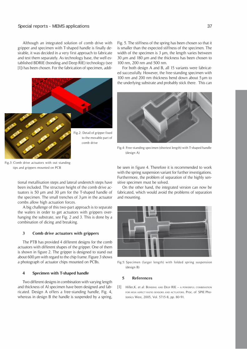
Comb drive actuators with grippers3
The PTB has provided 4 different designs for the comb actuators with different shapes of the gripper. One of them is shown in figure 2. The gripper is designed to stand out about 600 µm with regard to the chip frame. Figure 3 shows a photograph of actuator chips mounted on PCBs.
Specimen with T-shaped handle4
Two different designs in combination with varying length and thickness of Al specimen have been designed and fab-ricated. Design A offers a free-standing handle, Fig. 4, whereas in design B the handle is suspended by a spring,
Fig. 5. The stiffness of the spring has been chosen so that it is smaller than the expected stiffness of the specimen. The width of the specimen is 3 µm, the length varies between 30 µm and 180 µm and the thickness has been chosen to 100 nm, 200 nm and 500 nm.
For both design A and B, all 15 variants were fabricat-ed successfully. However, the free-standing specimen with 100 nm and 200 nm thickness bend down about 5 µm to the underlying substrate and probably stick there. This can
be seen in figure 4. Therefore it is recommended to work with the spring suspension variant for further investigations. Furthermore, the problem of separation of the highly sen-sitive specimen must be solved.
On the other hand, the integrated version can now be fabricated, which would avoid the problems of separation and mounting.
References5
Hiller,K. et al[1] : BonDing anD Deep rie – a powerful coMBination
for high aspect ratio sensors anD actuators. Proc. of SPIE Pho-
tonics West, 2005, Vol. 5715-8, pp. 80-91.
Special reports - MEMS applications 37

Fabrication processFig.1:
Introduction1
Ultrasonic transducer is a special kind of acoustic sen-sor. It can be used to detect and emit ultrasound. Most current ultrasonic transducers are made from piezoelec-tric ceramics, which can couple sound wave efficiently into solid materials, and detect cracks in them. Howev-er, because the impedance mismatch between ceramic and fluid is large, ceramic transducers become less ef-fective in airborne and immersion applications. In order to improve the energy conversion efficiency in these sit-uations, many efforts have been made [1, 2], but these improvements are mainly airborne-oriented. In this pa-per, we will investigate the feasibility of capacitive trans-ducer for immersion applications.
Experiment Investigation2
Figure 1 shows the fabrication steps of the proposed transducer. It consists of a membrane carrier and a back plate. Preparation of the membrane carrier starts from double side polished Si wafer. First, 500nm thermal ox-ide and 300nm LP-SiN are grown on the wafer surface. After that, 600nm Al is deposited and subsequently pat-terned. Before Al deposition, some via are opened in the oxide/nitride composite layer, so that electrical connec-tion can be realized in the future. In following steps, 2µm PE-SiO2 is deposited on the Al electrodes. This layer acts as passive layer, and it is then patterned to provide ac-cess windows for bottom electrode.
Fabrication of the back plate is relative simple. Alto-gether only 3 masks are used. First, 500nm thermal ox-ide is grown on (111)-type silicon wafer and sequentially patterned to act as etch mask. The wafer is then dipped in KOH solution to remove a thin silicon layer. Because surfaces exposed by KOH etching is very rough, these recesses have an inherent anti-stiction ability. The depth of the recesses is determined by etching time, and can be
varied between 2 to 7 µm. After KOH etching, the mask oxide is stripped off and a new oxide layer is grown on the wafer. In following step, 600 nm Al and 2 µm PE-oxide are sequentially deposited and patterned to form bottom electrodes. Finally, access windows are opened in the PE-oxide layer to expose contact pads.
When both components are ready, they are assem-bled together through direct bonding. Since direct bond-ing requires smooth surface finish, before bonding, a polish step may be necessary to eliminate protrusions and improve surface smoothness. After that, the wafer stack is dipped in KOH solution to remove bulk silicon above the composite membrane. Finally, an oxide etch-ing process is carried out to remove the protective ox-ide above the Al pads, so that electric connection can be established.
Initial Characterisation3
Figure 2 shows a microscopic photo of the proposed ultrasonic transducer. It has 7 identical cells. To facilitate future packaging process, contact pads are arranged in a seperate region beside the active cells. In Figure 2, one
Chenping Jia1, Maik Wiemer2, Karla Hiller1, Thomas Otto2, Thomas Gessner1,2 1Centre for Microtechnologies, Chemnitz University of Technology,
Chemnitz, Germany 2Fraunhofer IZM Chemnitz Branch, Chemnitz, Germany
Fabrication of a Low-Frequency Ultrasonic Transducer
38 Special reports - MEMS applications

Amplitude-Frequency responseFig.4:
Membrane static deformationFig.3:
Silicon micro-machined ultrasonic transducerFig.2:
The dynamic property of the transducer is measured with a laser Doppler vibrometer. According to this mea-surement, the resonant frequency of the transducer is 570kHz, and the maximal vibrating amplitude at res-onance is 1nm, with 10Vpp stimulus and 5Vdc bias. By changing the dimension, thickness, as well as the material composition of the membane, it is possible to extend the resonant frequency to 100kHz range. Si-miliarly, if large vibration amplitude is required, one can use larger stimulus signals.
Summary4
In this paper, an improved process for the fabrica-tion of capacitive ultrasonic transducer is proposed. Benefited from the separate preparation steps, low
frequency transducers of 100 to 500 kHz can be pro-duced without resorts to sacrifice etching. Two major aims were realized in this investigation. First, both top and bottom electrodes are arranged on the same side of the device. Therefore, no vertical via is required to address the bottom electrode. By employment of met-al electrodes, instead of bulk substrate electrode, con-tact resistance and parasitic capacitance are greatly re-duced. Besides, single side layout also facilitates future packaging and integration with electronics. Second, a self-stop etching scheme was proposed and success-fully implemented. With this method, regular recess-es of 2 to 7 microns depth can be produced on the surface of a standard (111) Si wafer. Moreover, since the bottom surface of these recesses is rough and un-even, it has inherent anti-stiction ability. For capaci-tive transducer that requires small and controllable
can also see an extra pad for ground electrode. Together with the bottom electrode, this pad provides a simple method for the formation of a matched capacitor.
Fig. 3 shows the static deformation of the mem-brane under the load of normal air pressure. Through
the interference rings, one can infer that the surface of the membrane is not flat. Further calculation indi-cates that the maximal deformation of the membrane at the center is more than 500nm, This means that her-
metic sealing has been realized during bonding, and the inner side of the membane is under vaccum con-dition. Note that due to bonding mis-alignment, the top and the bottom electrodes do not coincide fully with each other.
Special reports - MEMS applications 39

electrode gap, this method is especially valuable. In comparison with conventional surface processes for capacitive transducer, this method is simple, reliable and tolerable to process-parameter variances. It can be a potential method for the fabrication of underwater ul-trasonic transducers.
Acknowledgement5
The authors would like to express their appreciations to Mr. J. Grunert and S. Uhlig for their dedications in this work, and Mrs. M. Henker and I. Hoebelt for sample inspection. The supports of the colleagues in the Center for Microtechnologies (ZfM) at TU Chemnitz are also acknowledged.
Reference6
Scheeper, P. R.; van der Donk, A. G.; Bergveld, P.[1] : faBrication of silicon conDenser Microphones us-ing single wafer technology. J. Microeledtromech. Syst., vol. 1, No. 3, 1992.
Bergqvist, J.; Gobet, J.[2] : capacitive Microphone with a surface MicroMachineD Backplate using electro-plating technology. J. Microeledtromech. Syst., vol. 3, No. 2, 1994.
40 Special reports - MEMS applications

Principle of the used electrolysis-gel pump. The gas generated Fig.1:
by electrolysis is used to directly drive the fluid through the
channel system
Introduction1
A fully-integrated injection-moulded thermoplastic mi-crofluidic system complete with active pumps, sealing and controlled surface modification suitable for protein applications has been developed within the European research project SEMOFS. Microfluidic flow control in this system is realized by low-cost, low temperature, one-shot micropumps based on electrochemical gas genera-tion by electrolysis inside a hydrogel. As almost no heat is generated by this actuation principle, it is well suited for protein-sensing applications.
Electrolysis and Hydrogels2
The electrolysis of water is the dissociation of wa-ter molecules into oxygen and hydrogen gas by means of an electric voltage. The (net) reaction is given by:
Anode: 2H2O → 4H
+ + 4e
– + O
2 (gas)
Cathode: 2H2O + 2e
– → 2OH – + H
2 (gas)
The amount of generated gas molecules is directly proportional to the current flowing through the elec-trolytic cell. The generated gas can be either used to deflect a membrane or to drive a fluid by directly ap-plying the gas pressure to a fluid plug without an in-termediate membrane.
Bubble actuators based on electrolysis have al-ready been successfully demonstrated for microflu-idics. All these works have in common that a liquid (usually water or a water based liquid) has been used as electrolyte. Thus, an “actuation liquid” has to be integrated into the system. However, the integration of a liquid can be a critical factor for mass produc-
tion and may also cause problems concerning long-term stability.
Therefore, in this work a (water-containing) hydrogel is used as electrolyte instead of a liquid. By the usage of stencil printing, such a gel proved to be easy to integrate and thus highly suitable for mass fabrication.
Non-toxic and available at very low cost, a hydro-gel based on poly (acrylic acid) sodium salt (PAAS) was used.
Crosslinked PAAS is a so-called super absorbing poly-mer which is able to dramatically swell in water. The swollen state is referred to as a hydrogel, which mainly consists of up to 99 wt% of water, but has a very high viscosity. When PAAS is brought in contact with water, the weakly bonded sodium is split off, leaving negatively charged polymer chains and movable sodium ions:
Integration of active and passive microfluidics3
The whole microfluidic system consists of a passive microfluidic substrate and an electrode substrate as the actuator part.
As shown in Fig.1, the PAAS gel is placed directly on electrodes on the electrode substrate. Applying a volt-age over the electrodes leads to a gas generation due to electrolysis. The generated gas can then directly be
Joerg Nestler1, Karla Hiller1, Thomas Otto2, Thomas Gessner1,2
1 Center for Microtechnologies, Chemnitz University of Technology,
Chemnitz, Germany 2 Fraunhofer IZM Chemnitz Branch, Dept. Multi Device Integration,
Chemnitz, Germany
MICROFLUIDIC LOW-COST PUMPS BASED ON ELECTROLYSIS WITHIN HYDROGELS
Special reports - MEMS applications 41

Passive microfluidic substrateFig.2:
Assembly of active and passive micro-fluidics (top: principle, Fig.3:
bottom: assembled device)
Emptying sequence of a reservoir by an electrolysis-gel pump. Fig.4:
The small line in each picture marks the front of the colored
liquid plug inside the channel.
Results4
The pumps prepared as described above allow a back-pressure of more than 1 bar, flow rates in a typical range between 1 and 40 µl/min, and are able to deliver vol-umes of several 100µl. In Table 1 the characteristics of the low-cost pumps are summarized.
Parameter Value Unit
Flow Rate: 5 - 100(typ. 1 - 40)
µl/min
Max. Backpressure: 1..2 bar
Operating Current 0.5 - 10(typ. 4)
mA
Operating Voltage: < 15 (typ. 5)
V
Actuator Size (typ.): (3x3x0.2) mm³
Operating Time (per pump)
<10 min
Fig. 4 shows the emptying sequence of the middle of the three reservoirs.
Acknowledgements5
This work has been founded by the European Com-mission under contract number IST-FP6-016768 and is part of the European research project SEMOFS (Sur-face Enhanced Micro Optical Fluidic Systems, www.semofs.com).
used to drive liquids through the channel system in a flu-idic substrate.
In the passive microfluidic substrate, Fig. 2, each inlet reservoir is connected to the pump region by a thin hy-drophobic channel (“gas delivering channel”) of a cross
section of 100x100 µm², Fig. 2 & 3. The pump region mainly consists of the gel reservoirs on top of the elec-trode substrate.
After joining active and passive microfluidic parts, the inlet reservoirs can be filled by a syringe or a dispenser.
Performance of the integrated micropumpsTable1:
42 Special reports - MEMS applications

Basic principleFig.1:
Basic structure of the force coupled oscillator systemFig.2:
Introduction1
Detection of mechanical vibration is an important means for condition monitoring at industrial machinery for instance at gears, bearings, drives, engines and oth-er highly stressed machine components [1]. Changes e.g. in amplitude, frequency or both are indices of increas-ing wear. By observing these changes, maintenance can be scheduled and consequences of the machine failure are avoided.
Commonly, precision engineered wideband trans ducers or wideband MEMS sensor elements are used for vibra-tion detection. Together with signal analyzing electronics the spectral data of the time series is acquired. But, the high costs of these systems make permanent monitor-ing only reasonable for expensive equipment or in safe-ty related applications.
In most instances it is sufficient to observe only a few spectral lines for extracting the relevant information. Combining the frequency selectivity and the expected low manufacturing costs, micromechanical resonant vi-bration sensors are powerful means for this type of ap-plication [2]. The main drawback of the resonant sen-sors is that monitoring of the low frequencies requires either an extremely large chip area or a weak suspen-sion to reduce the stiffness to mass ratio for applications well below 1 kHz.
The new approach makes use of the superhetero dyne principle to transform the information of low frequency into an acceptable frequency range for resonant detec-tion, Fig. 1. The interaction of a wideband oscillator and a resonator makes it possible to detect low frequency vi-bration with a resonant principle. Simultaneously, it al-lows simple tuning of the detection frequency.
Principle of Operation2
The new sensor system consists of two separated micromechanical oscillators and is operated at stan-dard pressure. Electrostatic forces are used to couple the two oscillators, see Fig. 2.
One of the oscillators is used as a wideband detector for mechanical vibration. It is passively damped with
Roman Forke1; Dirk Scheibner2; Thomas Gessner3; Wolfram Dötzel1; Jan Mehner1 1Department of Microsystems and Precision Engineering,
Chemnitz University of Technology, Chemnitz, Germany, 2Siemens Automation and Drives, Advanced Technologies and
Standards, Nuremburg, Germany 3Center for Microtechnologies, Chemnitz University of Technology,
Chemnitz, Germany
Adjustable Force Coupled Sensor-Actuator System for Low Frequency Resonant Vibration Detection
Special reports - MEMS applications 43

Principle of operation Fig.3:
SEM view of the force coupled oscillator systemFig.4:
Frequency domain of the sensor outputFig.5:
Results4
To be free of any distracting mechanical coupling, the sensor system is tested using electrostatic excita-tion of the wideband oscillator. Fig. 5 shows the graph of a measurement taken with electrostatic excitation at 400 Hz and capacitive pick-off. For the high Q res-onator, the measured eigenfrequency is f0=29.87 kHz. By setting the carrier frequency to fc=30.27 kHz the 400 Hz excitation can be monitored.
The graph in Fig. 6 shows the linear dependence of sensor excitation and voltage output. The drive elec-trode of the mechanical receiver drives this oscillator with different voltages from 0 to 10 Vpp and at a fre-quency of 400 Hz.
fluidic damping structures. The second oscillator is a resonator with its eigenfrequency set to one decade above the latter. The principle can be summarized by the following three main steps [3]:
The mechanical signal of low frequency (up •to 1 kHz) is detected with a wideband, op-timally damped oscillator.
The motion of this oscillator is used to mod-•ulate the existing electrostatic force (carrier) between the two force coupled oscillators. Thus the low frequency information is trans-formed into a higher frequency range.
The carrier can be adjusted so that the res-•onator is excited at its resonance frequen-cy. This allows a frequency selective detec-tion of low frequency mechanical vibration, Fig. 3.
Fabricated Silicon Structure3
The micromechanical system is fabricated with the BDRIE (Bonding and Deep Reactive Ion Etching) silicon technology which allows aspect ratios of more than 25:1 and thus belongs to the HAR (High Aspect Ra-tio) technologies [4]. The single crystal line active wafer contains the mechanical elements as well as the drive and detection electrodes for lateral movement. Thick thermal oxide layers are used for vertical insulation. The lateral insulation is achieved by air gaps.
Fig. 4 shows a scanning electron microscopy (SEM) image of the fabricated silicon structure.
44 Special reports - MEMS applications
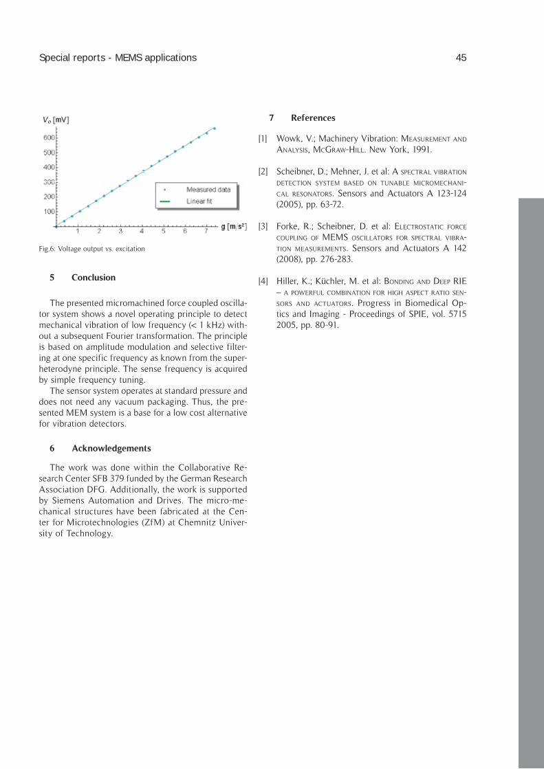
Voltage output vs. excitationFig.6:
References7
Wowk, V.; Machinery Vibration[1] : MeasureMent anD analysis, Mcgraw-hill. New York, 1991.
Scheibner, D.; Mehner, J. et al[2] : a spectral viBration Detection systeM BaseD on tunaBle MicroMechani-cal resonators. Sensors and Actuators A 123-124 (2005), pp. 63-72.
Forke, R.; Scheibner, D. et al[3] : electrostatic force coupling of MeMs oscillators for spectral viBra-tion MeasureMents. Sensors and Actuators A 142 (2008), pp. 276-283.
Hiller, K.; Küchler, M. et al[4] : BonDing anD Deep rie – a powerful coMBination for high aspect ratio sen-sors anD actuators. Progress in Biomedical Op-tics and Imaging - Proceedings of SPIE, vol. 5715 2005, pp. 80-91.
Conclusion5
The presented micromachined force coupled oscilla-tor system shows a novel operating principle to detect mechanical vibration of low frequency (< 1 kHz) with-out a subsequent Fourier trans formation. The principle is based on amplitude modulation and selective filter-ing at one specific frequency as known from the super-heterodyne principle. The sense frequency is acquired by simple frequency tuning.
The sensor system operates at standard pressure and does not need any vacuum packaging. Thus, the pre-sented MEM system is a base for a low cost alternative for vibration detectors.
Acknowledgements6
The work was done within the Collaborative Re-search Center SFB 379 funded by the German Research Association DFG. Additionally, the work is supported by Siemens Automation and Drives. The micro-me-chanical structures have been fabricated at the Cen-ter for Microtechnologies (ZfM) at Chemnitz Univer-sity of Technology.
Special reports - MEMS applications 45

Cross sectional view of the sensorFig.1:
Introduction1
Vacuum technology has become more and more im-portant for industrial production during the last years, particularly for surface coating and refinement. These applications require measurement systems with short measurement time and a measurement range of more than five decades. To control the charging of the re-cipients, sensitivity of the sensors up to ambient pres-sure (103 mbar) is desired.
Actual development of vacuum gauges considers these requirements by minimizing conventional gauges like Pirani and Cathode Manometers [1-2]. Some of these new sensors are already commercially available.
Friction gauges are used in high and fine vacuum as reference and calibration sensors. They utilize the damping of an oscillator by energy emission to the sur-rounding gas as a measure oft the pressure. Sugges-tions for MEMS friction gauges are described by Kurth [3] and Bianco [4].
In this work we present a new MEMS friction vac-uum gauge which expands the advantages of common friction gauges to a larger measurement range and a short measurement time. The sensor can be used for measurements in high temperature environments up to 350° C.
Assembly and working principle2
The working principle of the sensor is based on the pressure dependent gas friction. The essential part of the sensor is a torsional oscillating plate with a nearby wall. The structure of the sensor is shown in Figure 1. It con-sists of a 25 µm thick, 3x3 mm2 oscillating plate which is mounted in the centre of the chipframe by two 325 µm long torsional springs. The gap between oscillator and the electrodes on the carrier is 5 µm.
For detecting the vacuum pressure, we utilise two different kinds of pressure depending damping: For low pressures, where the gas can not be considered as a con-tinuum, the molecular damping is pressure dependent. For higher pressures, where the gas can be considered as a continuum, the squeeze damping is the pressure dependent one.
Below the oscillating plate is a hole in the carrier wa-fer for reducing the damping at higher pressures, so the plate will oscillate and not be overdamped at any pres-sure. At low pressures, the hole has no effect on the mo-lecular damping.
Due to a driving voltage between the oscillator (Elec-trode 1) and one of the ground electrodes (Electrode 2, resp. Electrode 3), the oscillator plate tilts around its ro-tation axis.
Simulation of the sensor3
The sensor can be considered as a system with one degree of freedom, because only the gyratory mode is of interest. The static and dynamic behaviour can be described by the differential equation
â ky + y + y = 0m m
(1)
The damping b consists of several components:Above 1 mbar the gas around the oscillator can be
treated as a continuum. In this pressure range, up to ambient pressure, the effective viscosity of the gas in
Dirk Tenholte1; Steffen Kurth2; Karla Hiller1; Christian Kaufmann1; Thomas Gessner1,2; Wolfram Dötzel1; Jan Mehner1 1Faculty of Electrical Engineering and Information Technology,
Chemnitz University of Technology, Chemnitz, Germany 2Fraunhofer IZM, Dep. Multi Device Integration, Chemnitz, Germany
A MEMS friction vacuum gauge
46 Special reports - MEMS applications

Simulated and measured decay constant depending on Fig.2:
pressure
Detection of the damping4
There exist two different ways to detect the pressure dependent damping of the sensor.
Determining the Decay Constant4.1
One option of determining the damping is to evaluate the damped oscillation. After switching off the driving voltage between oscillator and one of the ground elec-trodes, the damped oscillation
td
ˆ(t) e cos( t)−δφ = φ ⋅ ω (2)is measured. The decay con-
stant d is determined by detecting the maxima of the oscil-lation and calculating their logarithm. These values result in a straight line which gradient is the decay constant:
( ) ˆln t = ln - tφ φ δ (3)
To reduce the response time of the sensor, the mea-surement is stopped after 100 ms. If the oscillation am-plitude is above a given value after calculating the decay constant, another measurement is started without exiting the oscillator again. At pressures below 10-3 mbar, the decay constant has to be calculated by averaging from several 1000 measured values to reduce the influence of noise. So a measurement time of several seconds result, which is not acceptable for an industrial operation.
Controlled sensor operation4.2
Another way to detect the pressure dependent damp-ing is the controlled operation of the sensor. The os-cillation amplitude is adjusted to a constant value by controlling the amplitude of the sinusoidal driving voltage. The block diagram of the controlled sensor system is shown in Figure 3. If the driving voltage is connected to the oscillator and the ground electrodes, the damping and therefore the pressure is proportion-al to the squared driving voltage:
2eä ~ p ~ U (4)
So the variation of d over 7 decades, as shown in Figure 2, results in a variation of the driving voltage over 3.5 decades in the Range of 1 mV to 10 V.
To get a pressure dependency of the driving volt-age over the whole measurement range of the sensor, the oscillator has to be driven exact on its resonance frequency. The phase shift shown in Figure 3 corrects the phase error inducted by the measurement electron-
the narrow gap of 5 µm between oscillator and elec-trodes depends on the pressure. Due to the hole under the oscillator, only a narrow area at the two opposite ends of the oscillating plate parallel to the vibration axis, where oscillator and ground electrodes overlap, leads to the squeeze damping. Due to the small ampli-tude of oscillation, the motion of the plate towards the electrodes has to be regarded as translational. Meth-ods for numerical analysis of the squeeze damping for two parallel, towards moving plates are presented by van Kampen [5].
For pressures below 1 mbar, the mean free path of the gas molecules becomes much larger than the gap between oscillator and electrodes. In this pressure area the molecular damping occurs. We use the equations derived by Li [6] for calculating the molecular damping. They refer to a paddle formed structure, considered as a mathematical pendulum with lateral dimensions. The oscillator plate of our sensor can be approximated as two on their hinge concatenated paddles.
At the pressure range below 10-5 mbar, pressure independent kinds of damping like intrinsic and ther-mo compression damping reach the magnitude of the molecular damping and limit the lower measure-ment range.
On the basis of the developed simulation model the sensor geometry has been optimized, so that the mea-surement range is as wide as possible and the sensor is sensitive up to ambient pressure (103 mbar).
Simulated and measured decay constant of the opti-mized sensor is shown in Figure 2 depending on pres-sure. As one can see, simulation and measured values match very well. The sensor has a total measurement range over 8 decades from 10-5 mbar to 103 mbar.
Special reports - MEMS applications 47

Block diagram of the controlled sensor systemFig.3:
Comparison of pressure dependent decay constant and control Fig.4:
variable
Conclusions6
In this paper we have presented a new MEMS friction vacuum gauge. It has a measurement range of over 8 de-cades from 10-5 mbar up to ambient pressure (103 mbar). By using the controlled sensor operation, the response and measurement time can be lowered significantly
compared to the detection of damping by the damped oscillation. A response time of 10 ms and a measure-ment time of less than 150 ms can be realized.
The voltages used for sensor operation are ±12 V, so no electric or magnetic field is inducted to the ambient. The overall dimensions of the sensor are 8.5 mm x 9 mm x 1.5 mm; this complies with a volume of 115 mm3.
The sensor consists of silicon, glas and aluminium and can therefore be used for pressure measurement at high temperatures up to 350° C without any restric-tions. Unlike Pirani sensors it has no thermal affect to its ambient, but adopts the ambient temperature.
References7
Wilfert, S.; Edelmann, C.[1] : MiniaturizeD vacuuM gaug-es. J. Vac. Sci. Technol. A, Vol. 22, No. 2, Mar/Apr 2004, pp. 309-320.
Puers, R.; Reyntjens, S.; De Bruyker, D.[2] : the nanopi-rani – an extreMely MiniaturizeD pressure sensor faB-ricateD By focuseD ion BeaM rapiD prototyping. Sen-sors and Actuators A 87-89 (2002), pp. 208-214.
ics so that the oscillator is self-controlled and there-fore oscillates on its resonance frequency.
As a measure of the pressure, the control variable U
R is used. Its overshooting in case of pressure varia-
tions at low pressures can not be avoided, but it can be filtered by a low pass 2nd order. In this case, the response and measurement time only depends on the low pass. It is possible to realize a response time of
10 ms and a measurement time of less than 150 ms for large pressure variations. For continuous and steady pressure variations the measurement time is conspic-uously less.
Measurement results5
The sensor has been installed inside a vacuum sys-tem and the damping of the oscillator as well as the control variable have been measured as a function of the ambient pressure.
The measurement results are shown in Figure 4. Based on the scaling of the graphs, one can see that the gradient of the decay constant is twice the one of the control variable. The measurement range of the sensor reaches pressures below 10-5 mbar.
The sensor consists only of glas, silicon and alu-minium. These materials are temperature stable up to 400° C. Because the sensor electronics is connected to the sensor by an 1 m long cable, the sensor can be used for measurements at high temperatures. In-vestigations have shown that it is possible to use the sensor for pressure measurement at temperatures up to 350° C.
48 Special reports - MEMS applications
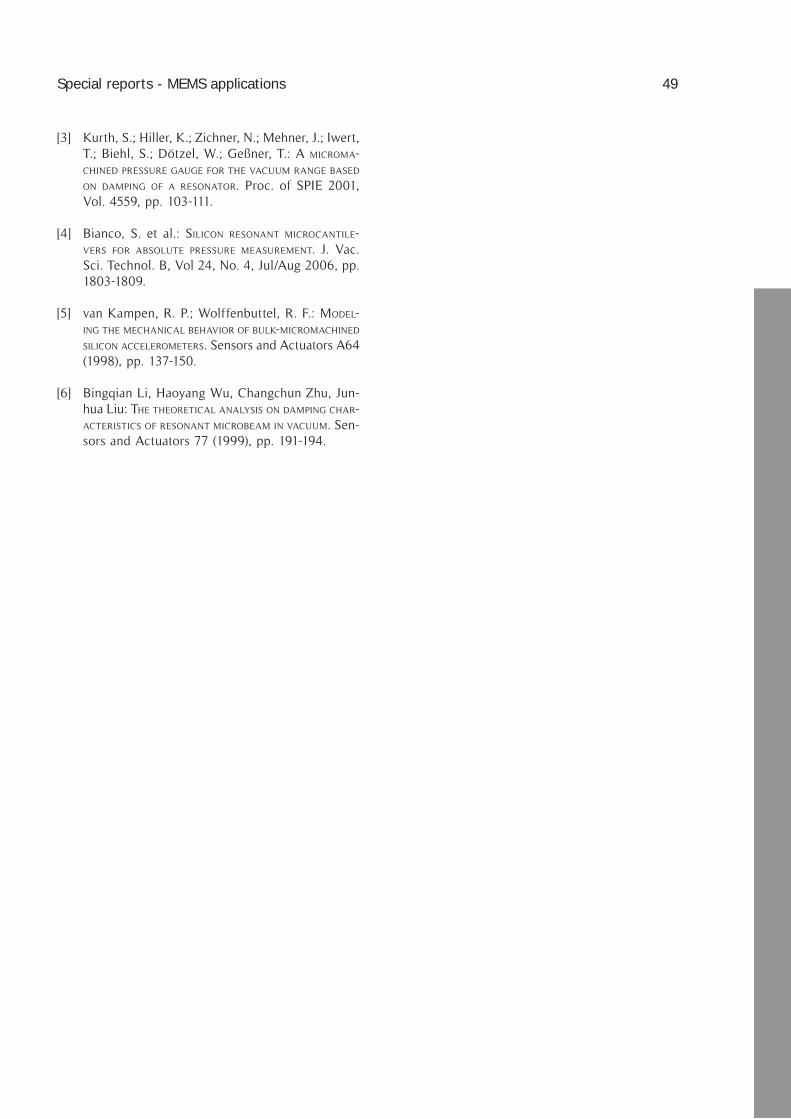
Kurth, S.; Hiller, K.; Zichner, N.; Mehner, J.; Iwert, [3] T.; Biehl, S.; Dötzel, W.; Geßner, T.: a MicroMa-chineD pressure gauge for the vacuuM range BaseD on DaMping of a resonator. Proc. of SPIE 2001, Vol. 4559, pp. 103-111.
Bianco, S. et al.[4] : silicon resonant Microcantile-vers for aBsolute pressure MeasureMent. J. Vac. Sci. Technol. B, Vol 24, No. 4, Jul/Aug 2006, pp. 1803-1809.
van Kampen, R. P.; Wolffenbuttel, R. F.[5] : MoDel-ing the Mechanical Behavior of Bulk-MicroMachineD silicon acceleroMeters. Sensors and Actuators A64 (1998), pp. 137-150.
Bingqian Li, Haoyang Wu, Changchun Zhu, Jun-[6] hua Liu: the theoretical analysis on DaMping char-acteristics of resonant MicroBeaM in vacuuM. Sen-sors and Actuators 77 (1999), pp. 191-194.
Special reports - MEMS applications 49
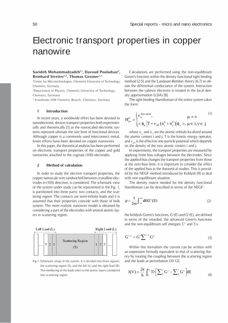
Schematic setup of the system. It is divided into three regions: Fig.1:
the scattering region (S), and the left (L) and the right lead (R).
The numbering of the leads refers to the atomic layers considered
into scattering region
Introduction1
In recent years, a worldwide effort has been devoted to nanoelectronic devices transport properties both experimen-tally and theoretically [1] as the nanoscaled electronic sys-tems represent ultimate the size limit of functional devices. Although copper is a commonly used interconnect metal, fewer efforts have been devoted on copper nanowires.
In this paper, the theoretical analysis has been performed on electronic transport properties of the copper and gold nanowires attached to the cognate (100) electrodes.
Method of calculation2
In order to study the electron transport properties, the copper nanoscale wire sandwiched between crystalline elec-trodes in (100) direction, is considered. The schematic view of the system under study can be represented in the Fig. 1, is partitioned into three parts: two contacts, and the scat-tering region. The contacts are semi-infinite leads and it is assumed that their properties coincide with those of bulk system. The more realistic nanowire model is obtained by considering a part of the electrodes with several atomic lay-ers in scattering region.
Calculations are performed using the non-equilibrium Green’s function within the density functional tight binding method [2-5] and the Landauer-Büttiker theory [6,7] to ob-tain the differential conductance of the system. Inter action between the valence electrons is treated in the local den-sity approximation (LDA) [8].
The tight binding Hamiltonian of the entire system takes the form:
free-atom
00 0
eff i j
,H
T (n n ) ,µ
µνµ ν
∈= < φ + ν + φ >
(1)
where and are the atomic orbitals localized around the atomic centers i and j; T is the kinetic energy operator, and
eff is the effective one-particle potential which depends
on the density of the two atomic centers i and j.In experiments, the transport properties are measured by
applying finite bias voltages between the electrodes. Since the applied bias changes the transport properties from those at the zero-bias limit, it is important to consider the effect of the applied bias in the theoretical studies. This is provid-ed by the NEGF method introduced by Keldysh [9] to deal with non equilibrium situation.
The density matrix needed for the density functional Hamiltonian can be described in terms of the NEGF:
(2)
the Keldysh Green’s functions, G<(E) and G>(E), are defined in terms of the retarded, the advanced Green’s functions and the non-equilibrium self energies < and >.
,, r aG G G< >< > = ∑ (3)
Within this formalism the current can be written with an expression formally equivalent to that of scattering the-ory by treating the coupling between the scattering region and the leads at perturbation [10-12].
2
1L L
2eI(V) Tr G G dEh
µ < >> <
µ = − ∑ ∑∫ (4)
Saeideh Mohammadzadeh1,*, Davoud Pouladsaz2, Reinhard Streiter1,3, Thomas Gessner1,3
1Center for Microtechnologies, Chemnitz University of Technology,
Chemnitz, Germany 2Department of Physics, Chemnitz University of Technology,
Chemnitz, Germany 3 Fraunhofer IZM Chemnitz Branch, Chemnitz, Germany
Electronic transport properties in copper nanowire
i, jµ = νµ∈ ν∈
50 Special reports - micro and nano electronics

Transmission spectra as a function of incident electron energy. Fig.2:
Diagrams (a) and (b) show the total transmission spectra at the
biases 0 and 1 V, for copper nanowire, respectively. The Fermi
energy is set to be 0 eV.
(5)
(6)
(7)
(8)
where ,
L
< >∑ are the self energy functions for the left contact. The limits of the integration,
1 and
2, are the electrodes
chemical potentials. It is assumed that the voltage drops across the scatter-
ing region, this assumption results in the contact self-ener-gies
( )
L(R)
< >∑ reducing to
2 Im( )<= −∑ ∑ r
L(R) L(R)L(R)if
2 (1 ) Im( )>= −∑ ∑ r
L(R) L(R)L(R)i f
where fL(R)
is the Fermi distribution function and r
L(R)Im( )∑
is the imaginary component of the retarded self–energy in the contact.
Based on the Landauer’s scattering approach to electron transport, and assuming that transport is ballistic for finite bias voltages, the current can be established by noting that the transmission matrix t() as
[ ] [ ]1/2 1/2rR Lt( ) ( ) G ( ) ( )ε = Γ ε ε Γ ε
where the L(R)
() is given by
†r rL(R) L(R) L(R)
( ) i( ( ) ( ) ) Γ ε = ε − ε ∑ ∑
By substituting the transmission matrix into equation (4) the current is obtained as follows
r aR L R L
2eI(V) Tr G G ( (E) (E))dEh
= Γ Γ − ∫ f f
where Tr[RGr
LGa] gives the transmission coefficients.
The differential conductance can be obtained from the current flowing through the system by taking the deriva-tive of current with respect to V [13-15].
In the adiabatic approximation, the zero bias voltage conductance at zero temperature can be written as G=G
0T,
where G0=2e2/h is quantum conductance and the factor T
represents the average probability that an electron injected at one end of the conductor will transmit to the other end.
Results and Discussion3
The transmission coefficients of the copper nanowire depicted in Fig. 1 for external bias voltages of 0-2 V have been calculated. The total transmission spectra as a func-tion of the electron incident energy for zero and 1.0 bias voltages applied to the system are shown in Figs. 2(a) and 2(b), respectively. The results indicate that the fluctuation
amplitudes of transmission spectra decrease by increas-ing the applied bias voltage, and the whole transmission spectra shift to lower energies in the presence of the ap-plied bias voltage.
The electronic transport properties of gold nanowire with the structure similar to copper nanowire are pre-sented to compare. The calculated I - V characteristics of each nanowire up to a bias voltage of 2.0 V as non-lin-
ear behaviour are shown in Fig. 3. One can see that the theoretical data of the current can be approximately fit into a cubic function of bias voltage drown with dotted lines in Fig. 3.
The numerical integration of equation (8), giving the total current, is carried out in order to obtain the differ-ential conductance by taking the integration step E = 0.01. Based on these calculations, the conductance of Cu and Au nanowires shown in Fig. 4 depends on the applied bias voltage and exhibits non-linearity response for both Cu and Au nanowires. The variation of the conductance is different for the two elements, which in Cu, G(V) var-ies by 9.24-5.64 and in Au varies by 5.68–3.62 in units of quantum conductance when the bias voltage increases.
Special reports - micro and nano electronics 51

Total current as a function of the applied bias voltage. Dotted Fig.3:
lines are the fitting characteristics.
Conductance as a function of external bias voltage for Cu and Fig.4:
Au nanowires.
Conclusions4
In summary, a theoretical analysis of the electronic trans-port properties of copper and gold nanowires sandwiched between crystalline electrodes in (100) directions has been performed by applying finite voltages, based on the non-equilibrium Green’s function within the density functional tight binding calculations. We have shown the dependency of the total transmission fluctuations on the incident elec-tron energy and applied bias voltages. The current-voltage characteristics of each system could be explained as a non-linear function and for the differential conductance in terms of the applied bias voltage the linear response is not valid. In comparison with copper nanowire, gold nanowire ex-hibits smaller electron conduction.
Acknowledgements5
We acknowledge Dr. Alessandro Pecchia for the helpful discussions, Dr. Thomas Niehaus for copper Slater-Koster
parameters, and the Deutsche Forschungsgemeinschaft for the financial support.
References6
Venkataraman, L.; Klare, J. E.; Nuckolls, C.; Hy-[1] bertsen, M. S.; Steigerwald, M. L., Nature, 442, (24) (2006), 904-907.
Frauenheim, T.; Seifert, G.; Elstner, M.; Niehaus, T.; Kohler, [2] C.; Amkreutz, M.; Sternberg, M.; Hajnal, Z.; Di Carlo, A.; Su-hai, S., J. Phys. Condens. Matter 14 (2002), 3015-3074.
Pecchia, A.; Di Carlo, A., Rep. Prog. Phys. 67 (2004), [3] 1497-1561.
Solomon, G. C.; Gagliardi, A.; Pecchia, A.; Frauen-[4] heim, Th.; Di Carlo, A.; Reimers, J. R.; Hush, N. S., J. Chem. Phys. 124, (094704) (2006), 1-10.
Pecchia, A.; Latessa, L.; Gagliardi, A.; Frauenheim, [5] Th.; Di Carlo, A.: Molecular nano electronics. J. M. Seminario, Elsevier, 2007, p. 205.
Datta, S.[6] : electronic transport in Mesoscopic systeMs. Cambridge University Press, NewYork, 1995, p. 48.
Büttiker, M.; Imry, Y.; Landauer, R.; Pinhas, S., [7] Phys. Rev.B 31(1985), 6207-6215.
Seifert, G.; Porezag, D.; Frauenheim, T., Int. J. Q. [8] Chem. 58 (1996) 185-192.
Keldysh, L.V., Sov. Phys. JEPT 20, 1018 (1965).[9]
Levy Yeyati, A., Phys. Rev. B 45 (1992) 14189-14196.[10]
Xue, Y.; Datta, S.; Ratner, M. A., Chem. Phys. [11] 281 (2002), 151-170.
Cuevas, J. C.; Yeyati, A. L.; Martin-Rodero, A., Phys. [12] Rev. Lett. 80 (1998), 1066-1069.
Glazman, L. I.; Khaetskii, A. V., Europhys. Lett. 9 [13] (1989), 263-267.
Castano,E., Kirczenow, G., Phys. Rev. B 41 (1990), [14] 3874-3877.
Martin-Moreno, L.; Nicholls, J. T.; Patel, N. K.; Pepper, [15] M., J. Phys. Condens. Matter 4 (1992), 1323-1333.
52 Special reports - micro and nano electronics

Process steps of the deposition and etchback technique to define Fig.1:
the transistor’s channel width (simulation results)
Introduction1
Regarding the International Technology Roadmap for Semiconductors [1], the down-scaling of the lateral fea-ture size of integrated MOS-transistors will continue for the next 15 years and reach a value below 10 nm. Al-though the resolution of optical lithography continually increases, up to now, no solutions for mass production of transistors with structure sizes below 40 nm with the needed accuracy and reproducibility exist.
In previous publications we already demonstrated a novel deposition and etchback technique which made it possible to produce transistors with a channel length down to 30 nm with excellent homogeneity and repro-ducibility and low demands to the used lithography [2-4]. With that technique only the channel length was ma-nufacturable in the sub-100 nm-region, not the channel width. We now modified and expanded the technique to generate transistors with channel length L and chan-nel width W in the sub-20 nm-region.
Structure Definition Process2
Fig. 1 shows the significant steps of the structure defi-nition of the MOS-transistor’s active area, which defines the channel width of the transistor. The cross sections were generated with the technology simulation software DIOS from ISE Integrated Systems Engineering Inc. [5]. First a pad-oxide is thermally grown and a nitride layer is deposited by LPCVD (Low Pressure Chemical Vapour Deposition) for the LOCOS technique (Local Oxidation of Silicon). On top of these layers a sacrificial polysilicon layer is deposited and structured by conventional optical lithography, Fig. 1a. The resolution of the applied lithog-raphy process is not important, because the resist mask only defines the local position of the transistor’s chan-nel area, but not the geometrical size (in this case chan-nel width) of the transistor.
Prof. Dr.-Ing. habil . John Thomas Horstmann Chair Electronic Devices of Micro and Nano Technique, Faculty for
Electrical Engineering and Information Technologies, Chemnitz
University of Technology, Chemnitz, Germany
Lithography Independent Fabrication of Nano-MOS-Tran sistors with Channel Width and Length in the Sub-20 nm-Region
Special reports - micro and nano electronics 53

SEM photo of the cross section of a 25 nm wide polysilicon Fig.3:
line fabricated with the presented deposition and etchback
technique
Cross section of a 100 nm wide active area, fabricated with the Fig.2:
modified deposition and etchback technique
After the removal of the resist mask a TEOS-oxide layer is deposited conformally, Fig. 1b, by LPCVD and etched back anisotropically in a special RIE-Process (Reactive Ion Etching) until a spacer surrounding the sacrificial ox-ide layer appears, Fig. 1c. The next step is the removal of the sacrificial polysilicon layer in an SF6-Plasma with high selectivity to all other layers followed by the trans-fer of the TEOS-nanostructure into the nitride and oxide layer by a high anisotropic RIE-process, Fig. 1d.
If the deposition process for the TEOS-oxide is ab-solutely conformal and the etchback process is ideal anisotropic, the linewidth is identical to the thickness of the prior deposited TEOS-oxide layer. However, if the real processes are not absolutely conformal respectively anisotropic, the linewidth is thinner but still reproduc-ible and exactly determined by the TEOS-oxide thick-ness. The accuracy and homogeneity of the line width is due to the well controllable layer deposition and etch-back techniques very high compared to other lithogra-phy techniques for such small structures. We achieve a uniformity of ± 1.5 % over a whole 4 inch wafer and of ± 3 % from wafer to wafer.
To prevent the lateral oxidation under the nitride mask (birds beak), a nitride spacer is formed on the vertical sidewalls of the masking layers by deposition and etch-back of a second nitride layer, Fig. 1e. This complete structure is used as mask for the local field oxidation, Fig. 1f. The width of the active area is defined by the thickness of the TEOS-oxide and by the thickness of the second nitride layer, not by any lithography. Due to the high accuracy of layer deposition techniques, sub-100 nm feature sizes with high precision and homogeneity are producible.
To generate active area structures with standard di-mensions, which are needed for larger transistors or for the contact regions of the Nano-Transistors, a resists mask is structured by normal lithography before the TEOS is etched back.
Figure 2 shows a SEM-photo (Scanning Electron Mi-croscope) of the cross section of an early sample after the local oxidation. In the center the active area surrounded by the field-oxide can be seen. The nitride layer for the masking during the local field oxidation is still on top of the active area.
After the removal of the masking layers by wet etching in hot phosphoric acid and HF-solution the gate- oxide is formed by thermal oxidation and the polysilicon layer is deposited by LPCVD. For the nano-MOS-transistors this poly silicon layer is structured with a similar deposi-tion and etchback technique, while larger structures are masked by a normal optical lithography.
We already presented the deposition and etch back technique for the polysilicon gate electrode before [2-4].
54 Special reports - micro and nano electronics

Significant steps of the deposition and etchback technique for Fig.4:
the gate definition
Microscopic photo of an MOS-transistor with W and L in Fig.5:
the sub-50 nm-region, the arrow indicates the active channel
region
In this case TEOS-oxide is used as sacrificial layer and nitride is used as masking layer. With the materials of the first deposition and etchback technique masking of a polysilicon layer would not be possible.
Figure 3 presents the significant steps of that structure definition technique, which defines the channel length of the MOS transistor with sizes in the deep-sub-100 nm-region and high accuracy of the line width.
Figure 4 shows a SEM-photo of a 25 nm wide poly-silicon line which was structured by the presented de-position and etchback technique.
The deposition and etchback technique can only gen-erate closed loops of sub-100 nm-wide lines. So addition-ally to the wanted sub-100 nm-features unwanted para-sitic lines occur and cannot be avoided directly. The red
arrow in Figure 5 indicates the location of the wanted active channel region.
The parasitic polysilicon line has no significant nega-tive influence. The capacity of this line is very low com-pared to the gate electrode due to the thick field oxide between the line and the substrate.
Conclusion3
A technique to fabricate real “Nano-Transistors” – MOS transistors with the channel length and the chan-nel width in the sub-50 nm-region – with low demands to the used lithography has been developed. Main idea of this technique is to use optical lithography only to define the local placement of the transistor, while the channel length and width are both defined by deposi-tion and by etching processes with a high precision in the sub-50 nm region. The standard deviation of the linewidth is about 1.5 % on a 4 inch wafer, and around 3 % from wafer to wafer. Only standard CMOS pro-cess equipment is used and only a few additional pro-cess steps compared to a standard CMOS process are necessary, so the technique is easily transferable to any other CMOS process line.
References4
Semiconductor Industry Association[1] : internation-al technology roaDMap for seMiconDuctors. San Jose, 2007.
Horstmann, J. T.; Hilleringmann, U.; Goser, K.[2] : noise analysis of suB-100 nM-Mos-transistors faBricateD By a special Deposition anD etchBack technique. Pro-ceedings of the 26th Annual Conference of the IEEE Industrial Electronics Society IECON-2000, October 22 - 28, 2000, Nagoya, Japan, pp. 1867 - 1872.
Horstmann, J. T.; Hilleringmann, U.; Goser, K.[3] : 1/f noise of suB-100 nM-Mos-transistors faBricateD By a special Deposition anD etchBack technique. Micro and Nanoengineering MNE’99, September 21 - 23, 1999, Rome, Italy, pp. 213 - 216.
Horstmann, J. T.; Hilleringmann, U.; Goser, K. F.[4] : Matching analysis of Deposition DefineD 50 nM Mos-fet’s. IEEE Transactions on Electron Devices, Vol. 45, No. 1, January 1998, pp. 299 – 306.
ISE Integrated Systems Engineering Inc.[5] : Diosise version 6.0, reference Manual of the two-DiMensional technology siMulator. Zurich, Switzerland, 1999.
Special reports - micro and nano electronics 55

Interface structure model of Si/SiOFig.1: 2/Si system and the positions
of five different oxygen (dark balls) vacancies
Introduction1
Improving the performance of metal-oxide-semicon-ductor field effect transistor (MOSFET) devices in terms of a higher degree of integration and faster devices has required a larger gate capacitance for each new technol-ogy generation. To date, this has been achieved main-ly by decreasing the gate oxide thickness, which has reached values as small as 1.5 nm. Gate tunneling cur-rent is a major problem at this thickness limit. Such ul-trathin layers consist of few atomic layers and therefore within the scope of first principle atomic-scale models. Furthermore, applying an atomic-scale approach pro-vides a method to investigate atomic scale bonding, dis-locations and vacancies, as well as their influence on the tunneling current.
In the following report, a combination of density func-tional theory (DFT) and ballistic transport theory within the non-equilibrium Green’s function formalism is applied to the calculation of a Si/SiO
2/Si model interface and the
tunneling current through this structure, containing dif-ferent oxygen vacancies.
Atomistic structural model2
In most electronic structure calculations different phases of crystalline SiO
2 have so far been employed
to generate model interfaces, mainly b-quartz, b-cristo-balite and tridymite. We started with crystalline SiO
2 b-
cristobalite to model the gate oxide. SiO2 b-cristobalite
has a slightly larger lattice mismatch (about 6%) to Si (001) than tridymite, however, cubic cristobalite has a lot of polymorphs that are almost energetically degenerate
and differ only by relative rotations of the SiO4 tetrahe-
dral units. Thus it can adjust easily to stress and to local distortions e.g. due to a vacancy. The mismatch is min-imized if the SiO
2 crystal is rotated by 45° around its c
axis. Thus, the lateral lattice constant of SiO2 was fixed
(expanded) to the value of √2×aSi and the cristobalite cell was relaxed along its c direction. From the “tetrag-onal” b-cristobalite bulk structure that was produced by this procedure, a slab consisting of seven layers of SiO
2
was composed and put on the Si substrate consisting of nine layers of Si, as shown in Fig. 1. These numbers of atomic layers ensure that bulk properties are recovered in the respective slabs and that the interface does not in-teract with its periodic image. Note that the interface at the right hand side of the supercell is equivalent to the one in the left hand side, but rotated by 90° around the z direction of the supercell (the direction perpendicular to the interface).
To make up for the undercoordination of Si at the in-terface to SiO
2, extra bridging oxygen atoms were add-
ed, completing the coordination. As pointed out in refer-ence [1] by ensuring the preferred coordination number for each Si atom the interface energy is minimized. In this case this also leads to a formal oxidation state +2 of Si at the interface, which is one of the intermediate oxidation states that have been observed experimentally [2].
Different initial separations between the last layer of Si in the substrate and the first layer of Si in SiO
2 were
chosen. For all the different configurations the atomic positions were relaxed. In the minimum energy config-uration the separation between the last layer of Si in Si
Ebrahim Nadimi1, Rebecca Janisch2, Enver Nakhmedov1, Philipp Plänitz1, Rolf Öttking1, Fafa Chiker1, Frank Thunecke1, Martin Trentzsch3, Karsten Wieczorek3, Christian Radehaus1
1 Opto- and solid state electronics, Faculty for Electrical
Engineeringand Information Technologies, Chemnitz University
of Technology, Chemnitz, Germany 2 Department of Materials Science and Engineering, Friedrich-
Alexander-University Erlangen-Nuremberg, Germany 3AMD Saxony LLC & Co. KG, Dresden, Germany
First principle approach to the calculation of tunneling current in MOS Structures in the presence of oxygen vacancies
56 Special reports - micro and nano electronics
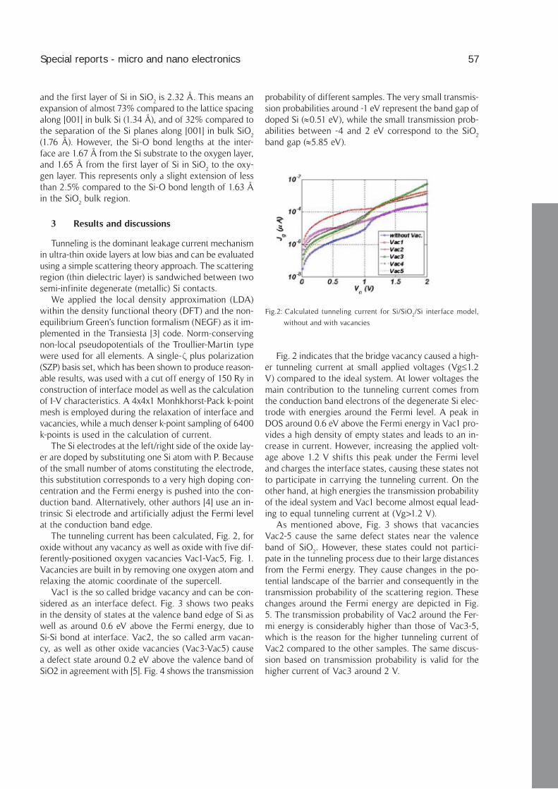
Calculated tunneling current for Si/SiOFig.2: 2/Si interface model,
without and with vacancies
and the first layer of Si in SiO2 is 2.32 Å. This means an
expansion of almost 73% compared to the lattice spacing along [001] in bulk Si (1.34 Å), and of 32% compared to the separation of the Si planes along [001] in bulk SiO
2
(1.76 Å). However, the Si-O bond lengths at the inter-face are 1.67 Å from the Si substrate to the oxygen layer, and 1.65 Å from the first layer of Si in SiO
2 to the oxy-
gen layer. This represents only a slight extension of less than 2.5% compared to the Si-O bond length of 1.63 Å in the SiO
2 bulk region.
Results and discussions3
Tunneling is the dominant leakage current mechanism in ultra-thin oxide layers at low bias and can be evaluated using a simple scattering theory approach. The scattering region (thin dielectric layer) is sandwiched between two semi-infinite degenerate (metallic) Si contacts.
We applied the local density approximation (LDA) within the density functional theory (DFT) and the non-equilibrium Green’s function formalism (NEGF) as it im-plemented in the Transiesta [3] code. Norm-conserving non-local pseudopotentials of the Troullier-Martin type were used for all elements. A single-z plus polarization (SZP) basis set, which has been shown to produce reason-able results, was used with a cut off energy of 150 Ry in construction of interface model as well as the calculation of I-V characteristics. A 4x4x1 Monhkhorst-Pack k-point mesh is employed during the relaxation of interface and vacancies, while a much denser k-point sampling of 6400 k-points is used in the calculation of current.
The Si electrodes at the left/right side of the oxide lay-er are doped by substituting one Si atom with P. Because of the small number of atoms constituting the electrode, this substitution corresponds to a very high doping con-centration and the Fermi energy is pushed into the con-duction band. Alternatively, other authors [4] use an in-trinsic Si electrode and artificially adjust the Fermi level at the conduction band edge.
The tunneling current has been calculated, Fig. 2, for oxide without any vacancy as well as oxide with five dif-ferently-positioned oxygen vacancies Vac1-Vac5, Fig. 1. Vacancies are built in by removing one oxygen atom and relaxing the atomic coordinate of the supercell.
Vac1 is the so called bridge vacancy and can be con-sidered as an interface defect. Fig. 3 shows two peaks in the density of states at the valence band edge of Si as well as around 0.6 eV above the Fermi energy, due to Si-Si bond at interface. Vac2, the so called arm vacan-cy, as well as other oxide vacancies (Vac3-Vac5) cause a defect state around 0.2 eV above the valence band of SiO2 in agreement with [5]. Fig. 4 shows the transmission
probability of different samples. The very small transmis-sion probabilities around -1 eV represent the band gap of doped Si (≈0.51 eV), while the small transmission prob-abilities between -4 and 2 eV correspond to the SiO
2
band gap (≈5.85 eV).
Fig. 2 indicates that the bridge vacancy caused a high-er tunneling current at small applied voltages (Vg≤1.2 V) compared to the ideal system. At lower voltages the main contribution to the tunneling current comes from the conduction band electrons of the degenerate Si elec-trode with energies around the Fermi level. A peak in DOS around 0.6 eV above the Fermi energy in Vac1 pro-vides a high density of empty states and leads to an in-crease in current. However, increasing the applied volt-age above 1.2 V shifts this peak under the Fermi level and charges the interface states, causing these states not to participate in carrying the tunneling current. On the other hand, at high energies the transmission probability of the ideal system and Vac1 become almost equal lead-ing to equal tunneling current at (Vg>1.2 V).
As mentioned above, Fig. 3 shows that vacancies Vac2-5 cause the same defect states near the valence band of SiO
2. However, these states could not partici-
pate in the tunneling process due to their large distances from the Fermi energy. They cause changes in the po-tential landscape of the barrier and consequently in the transmission probability of the scattering region. These changes around the Fermi energy are depicted in Fig. 5. The transmission probability of Vac2 around the Fer-mi energy is considerably higher than those of Vac3-5, which is the reason for the higher tunneling current of Vac2 compared to the other samples. The same discus-sion based on transmission probability is valid for the higher current of Vac3 around 2 V.
Special reports - micro and nano electronics 57

Density of states of the ideal system (thick line-blue) and those Fig.3:
containing Vac2-5 (upper-panel) as well as the system containing
Vac1 (lower panel)
Transmission probability of the ideal system and those containing Fig.4:
Vac1-5
Transmission probability of the ideal system and those containing Fig.5:
vacancies
Brandbyge, M.; Mozos, J.-L.; Ordejon, P.; Taylor, J.; [3] Stokbro, K.: Density-functional MethoD for nonequi-liBriuM electron transport. Phys. Rev. B, vol. 65, pp. 165401-1-17, 2002.
Demkov, A. A.; Zhang, X.; Drabold, D. A.[4] : towarDs a first-principles siMulation anD current-voltage charac-teristic of atoMistic Metal-oxiDe–seMiconDuctor struc-tures. Phys. Rev. B, vol. 64, pp. 125306-1-4, 2001.
Städele, M.; Tuttle, B.R.; Hess, K.[5] : tunneling through ultrathin sio
2 gate oxiDes froM Microscopic MoDels.
J. Appl. Phys., vol. 89, pp. 348-363, 2001.
In general all different vacancies are shown to cause an increase in the tunneling current either due to a higher DOS at the conduction band (Vac1) or higher transmission probability around the Fermi energy (Vac2-5). However the bridge vacancy seems to affect the tunneling pro-cess only at low applied biases, and acts like an interfa-cial state, while the arm vacancy has the most destruc-tive effect on the tunneling current at biases under 1 V. Bulk vacancies (Vac3-5) show almost the same behavior with small discrepancies at low and high biases.
Conclusions4
A combination of DFT and NEGF theory is applied to the construction and calculation of tunneling current through a Si/SiO
2/Si interface model. Several oxygen va-
cancies are created at different positions in the model structure and their influence on the tunneling current has been studied. The interface vacancy (Vac1) leads to higher tunneling current only at low biases, while bulk oxide vacancies cause an overall increase in tunneling current. The arm vacancy produces the highest tunnel-ing current at low biases.
References5
Tu, Yuhai; Tersoff, J.[1] : structure of the silicon-ox-iDe interface. Thin Solid Films, vol. 400, issues 1-2, pp. 95-100, 2001.
Himpsel, F.J.; McFeely, F.R.;Taleb-Ibrahimi, A.; Yar-[2] moff, J.A.; Hollinger, G.: Microscopic structure of the sio
2/si interface. Phys. Rev. B, vol. 38, pp.
6084-6096, 1988.
58 Special reports - micro and nano electronics

Polar and nonpolar parts and the total surface energy of the Fig.1:
evaluated solid surfaces of set 1 and 2 *
Nicole Ahner1, Matthias Schaller2, Christin Bartsch2, Eugene Baryschpolec3, Stefan E. Schulz1,4 1Center for Microtechnologies, Chemnitz University of Technology,
Chemnitz, Germany, 2AMD Saxony LLC & Co. KG, Dresden, Germany, 3Air Products, Lasne, Belgium. 4Fraunhofer IZM Chemnitz Branch, Chemnitz, Germany
Surface energy and wetting behaviour of plasma etched porous SiCOH surfaces and plasma etch residue cleaning solutions
Introduction1
With decreasing feature sizes and usage of po-rous low-k materials within the interconnect system the removal of plasma etch residues becomes a great challenge [1]. Plasma ashing processes using oxidiz-ing chemistries damage the low-k materials and are not able to remove inorganic parts of the residues [2]. Wet cleaning seems to be an alternative, but high as-pect ratio features and low energy residue surfaces quite often are not or poor wetted by the cleaning so-lution [3]. In this work the energetic characteristics of etch residue surfaces, differently plasma etched and stripped low-k dielectric surfaces and several cleaning solutions have been studied to evaluate their wetting behaviour. Additionally contact angle measurements using the cleaning liquids on the studied surfaces have been performed to compare the data.
Experimental2
Two sets of solid surfaces, provided by AMD, have been studied. Set 1 consists of three blanket etch poly-mer surfaces generated by a polymerizing plasma etch process using a CF-containing chemistry for 10, 15 and 30 sec. For set 2 porous SiCOH surfaces have been treated by different plasma etching/stripping process-es: a 20 sec. etch process, plasma strip 1 and 2 (PS1 and PS2, both reducing) and plasma strip 3 (PS3, ox-idizing). Additionally an untreated p-SiCOH surface has been investigated. The cleaning liquids have been provided by Air Products: four commercially available solutions (A: EZSTRIP 511, B: EZSTRIP 520, C: EZ-STRIP 530, D: NAC-1) and two experimental liquids (E, F). The surface energy of the solids has been de-
termined using the method of Owens, Wendt, Rabel and Kaelble [4]. The total surface energy of the liq-uids has been determined by the pendant drop meth-od. The nonpolar part of the surface energy has been calculated using contact angle measurement of the liquid on a PTFE-surface to eliminate the polar part from calculation [5]. Finally the wetting behaviour of the cleaning solutions has been tested on the surfac-es of the samples of set 1 and 2. All contact angle measurements have been performed using the KRUSS DSA-100 system.
Calculation and Results3
Surface Energy. The surface energy of the solid surfaces was calculated from the measured contact angles using the software of the DSA-100. Figure 1 shows the total surface energies and the polar and nonpolar parts. The examined surfaces are quite low-energetic, the untreated ULK surface is nearly com-
pletely nonpolar, while the other etched surfaces have a polar part. The nonpolar/polar ratio is changing with different etching processes, leading to a nearly 80% polar surface for PS3. This also leads to an increase of the total energy.
Special reports - micro and nano electronics 59

Calculated polar and nonpolar parts and the total surface energy Fig.2:
of the cleaning solutions A-F *
Measured contact angles of the cleaning liquids on the solid Fig.3:
surfaces of set 1 and set 2 *
The etch polymer surfaces do not change their to-tal energy but move towards nonpolar character with increasing process time. The cleaning solutions show very different energetic characters, Fig. 2. Liquids A and B have low surface energies, liquids C and D show me-dium surface energy values, while liquids E and F have quite high energies, near to the value of water (72.5 mN/m). The polar and nonpolar part of the liquid’s sur-face energy was determined using a PTFE plate, which is nearly complete nonpolar. So the polar part can be set to zero in the calculation and by measuring the con-tact angle of the liquid on the PFTE the nonpolar part is the only unknown value as visible in Eq. 1 (g
1d: non-
polar part of the liquid’s surface energy, g1: total sur-
face energy of the liquid, gSd: nonpolar part solid’s sur-
face energy, q: contact angle)
2d 1
1 dS
( (cos 1))4
γ ⋅ θ +γ =
⋅ γ(1)
By subtracting the nonpolar part from the total sur-face energy one gets the polar part. The high surface energies of cleaning liquids are a problem if the sur-face which should be wetted has a low energy. For example water, a very polar liquid with high surface energy, does not wet a PTFE-surface at all. Addition-ally the energetic characteristic of liquids and surfaces should be comparable to achieve good wetting. Thus by calculating the surface energies of solids and liq-uids one can make a prediction, which cleaning liquid will provide a good wetting and therefore an effective cleaning. On the other hand, determining the energy of a treated surface can tell a lot about the impact of this process on the surface.
Wetting behaviour. The measured contact angles on the plasma etched/stripped surfaces are shown in Figure 3. Liquid A and B show the best wetting behav-iour, both having the lowest contact angles. In some cases they even show complete wetting. The contact an-gles are much higher for all the other liquids, becoming larger with increasing surface energy of the liquid. The untreated porous ULK surface is an exceptional exam-ple because this surface has no polar energy-part. All liquids show high contact angles on this surface, some do not wet it at all. On the other hand higher surface energies of the solid lower the contact angle, as clearly to be seen for the PS3-surface. The polar and nonpo-lar parts of the surface energies also contribute to the wetting behaviour. For the low-energy-liquids A and B no clear trend is visible, but for all other liquids a de-creasing polar part of the solid surface increases the contact angle. This effect is very strong in exceptional situations like for the nonpolar ULK dielectric surface. An increasing polar energy part seems to increase the total energy of a surface as to been seen for the sur-faces after PS2 and PS3. Creating a new interface be-tween liquid and solid (wetting) will only happen if the whole system can lower its total energy by doing so [6]. From this point it is clear that a high energy liquid will not wet a low-energy surface and this is also the reason why the increase of the surface energy of the “PS3-sample” lowers the contact angle of the cleaning liquid. Additionally the polar energy part of a liquid can only interact with the polar part of a solid surface, which is also true for the nonpolar parts [5]. Because all of the tested liquids have a polar part the change of the contact angles on solid surfaces with different po-lar energy parts can be due to this effect.
60 Special reports - micro and nano electronics

*All graphics have been generated by IZMConclusions4
The energetic character of plasma etch polymer sur-faces and differently plasma etched/stripped p-SiCOH surfaces has been evaluated by contact angle measure-ment. The solid surfaces have a quite low energy and change their energetic character after different treat-ments. The evaluated cleaning solutions show very dif-ferent energetic characters, from low surface energy for liquid A and B to water-like surface energies for liquid F. The calculation of the surface energies of the solid sur-faces and the liquids provides the possibility to make a prediction regarding the wetting behaviour of a special combination of surface to be cleaned and cleaning solu-tion to be used. The wetting experiments show, that at first the total energy of the liquid is the major contributor to wetting behaviour: the lower the energy of the liquid the better the wetting. But also the ratio polar/nonpolar energy contributes to wetting. Due to their low surface energy liquid A and liquid B are best suited to clean sur-faces after etching and/or ashing.
Acknowledgement5
The project described in this publication has been funded in line with the technology funding for region-al development (ERDF) of the European Union and by funds of the Free State of Saxony.
References6
Fury, M.A.[1] : post-etch cleaning technology for cop-per / low-k applications. ISTC September 2004, Shanghai.
Myneni, S.[2] : post-plasMa-etch resiDue reMoval us-ing co
2-BaseD fluiDs. J. Electrochem. Soc. 150(12)
(2003), G744-G750.
Levitin, G.[3] : potoresist anD etch resiDue reMoval - effect of surface energy anD interfacial tension. J. Electrochem. Soc. 153(7) (2006),G712-G720.
Owens, D.K.[4] : estiMation of the surface free ener-gy of polyMers. J. Appl. Polymer Science 13 (1969), pp. 1741-1747.
Timmons, C.L.; Thesis at Georgia Tech, 2004.[5]
Preussler, W.[6] : oBerflächenspannung - MessMeth-oDen iM vergleich. Journal für Oberflächentechnik 10 (2002), pp. 106-108.
Special reports - micro and nano electronics 61

Introduction1
State of the art modeling and simulation tools al-low for behavioral analyses of microstructures with fixed dimensions and material properties. Sensitiv-ity analysis and layout optimization require a series of finite element (FE) simulations and subsequent function fit procedures in order to find the relation-ship between design parameters and component be-havior. Especially for a large number of design vari-ables, data sampling and function fit becomes time consuming and prone to errors [1].
The ultimate goal of MEMS component level de-sign is to obtain a macromodel from these accurate results that exhibits just input/output interface termi-nals of a device by means of internal state variables and can be directly linked into the circuit and sys-tem-level schematic. The deformation state and dy-namics of flexible electro-mechanical systems can be described efficiently by modal superposition meth-ods. In this technique, the deformation state of the structural domain is described by a weighted com-bination of linear mode shapes. Capacitance func-tions with regard to modal amplitudes provide non-linear coupling between the modes and the electrical quantities, such us electrostatic forces and current. Currently, ROM macromodels are generated by nu-merical data sampling and subsequent fit algorithms. Each data point must be obtained by a set of sepa-rate FE runs in the structural, electrostatic and flu-id domains [2].
Advanced parametric modeling technologies based on differentiation of the FE equations have been inves-tigated for mechanical and coupled domain systems in order to improve the computational efficiency of the MEMS reduced-order macromodel generation pro-cess. In particular, the time consuming data sampling process in the static and frequency response domains
has been replaced by a single finite element run on the basis of the structural, electrostatic and squeeze film analyses with regard to modal amplitudes.
Description of the Method2
The key idea of the new approach, which account for parameter variations in a single FE run, is to com-pute not only the governing system matrices of the FE problem but also their partial derivatives with regard to design variables [3].
Difficulties arose mainly from the fact that extrac-tion of high order derivatives (HOD) becomes nu-merical unstable and time consuming. Automatic dif-ferentiation (AD) is known as efficient mathematical algorithm to compute and handle high order deriva-tives of complicated systems. In contrast to symbolic differentiation which propagates mathematical func-tions, AD evaluates just numerical numbers extracted at the initial position needed for Taylor series expan-sion. Differentiation rules describe how to combine partial derivatives in order to form elementary math-ematical operations and where to store results in a 3-dimensional array.
As result, Taylor vectors or Pade approximation of the model response can be expanded in the vicin-ity of the initial position with regard to dimensional and physical design variables. The following diagram, Fig.1, explains the generation process. A test load is applied to the model to simulate the primary motion of the device. Then a modal analysis is performed to compute the mode shapes
i(x,y,z). The test load de-
flection {u(x,y,z)} is compared with the mode shapes
i(x,y,z) in order to select modes which become the
state variables of the macromodel. The derivatives of the parameters, characterizing flexible electro-me-chanical systems, are extracted from the FE matrices by means of the AD. By using the HOD method, the simulation results become directly polynomial func-tions in terms of modal amplitudes. Numerical results demonstrate that the generated models are highly ac-curate in a wide range of modal amplitudes. Taylor series coefficients of the strain energy, mutual capac-itances and damping ratios are store in ROM database for further use [4].
Vladimir Kolchuzhin; Wolfram Dötzel; Jan Mehner
Department of Microsystems and Precision Engineering,
Faculty of Electrical Engineering and Information Technologies,
Chemnitz University of Technology, Chemnitz, Germany
Efficient Generation of MEMS Reduced-Order Macromodels Using Higher Order Sensitivity Finite Element Technique
62 Special reports - design

Overview of the data generation for MEMS reduced order macromodel by HOD FE techniqueFig.1:
Conclusion3
The advanced simulation technique using differenti-ation of the discretized FE equations to automatic gen-erating of macromodels has been developed. In linear case, the reduction in expected generation time was at least two times.
It is necessary to point out the necessity for addi-tional memory, parametric mesh-morphing procedures and an access to the source FE code.
The HOD parametric FE technique is a promising al-ternative to existing data sampling and function fit pro-cedures utilized for MEMS parametric model extrac-tion from ordinary FE analyses. The algorithms support static, modal and harmonic analyses of structural, elec-trostatic, thermal and fluidic domains. Further work will be focused on extension of the method to nonlin-ear case and automated generation of the parametric ROM macromodels.
References4
Mehner, J.; Bennini, F.; Doetzel, W.[1] : caD for Micro-electroMechanical systeMs - systeM Design autoMa-tion: funDaMentals, principles, MethoDs, exaMples. Kluwer Academic Publ., pp. 111-132, 2000.
Bennini, F.; Mehner, J.; Dötzel, W.[2] : systeM level siMu-lations of MeMs BaseD on reDuceD orDer finite ele-Ment MoDels. Int. Journal of Computational Engineer-ing Science, Vol. 2, No. 2 (2003), pp. 385-388.
Kolchuzhin, V.; Mehner, J.; Gessner, T.; Dötzel, W.[3] : application of higher orDer Derivatives MethoD to paraMetric siMulation of MeMs. Proc. of 8th Int. Conf. EuroSimE, London, Great Britain, Apr. 2007, pp. 588-593.
Kolchuzhin, V.; Doetzel, W.; Mehner, J.[4] : efficient generation of MeMs reDuceD-orDer MacroMoDels using Differentiation of finite eleMents. Sensor Lett., Vol. 6, No. 1, pp. 97–105, 2008.
Special reports - design 63

Schematic of 1D-micro mirrorFig.1:
Introduction1
This article describes the design requirements at integrated high-voltage amplifiers for large MEMS based arrays consisting of electro sta tic driven actuators. Such actuators will be applied in optical switching arrays for cross connects in wavelength-division multiplexing (WDM) networks.Important properties of these integrated high-vol tage amplifiers are power consumption and waste heat. In particular the chip area must be small enough to facilitate the system integration with MEMS based switching arrays.
Besides a new calculation approach for efficien cy of amplifier operation modes a new concept of level-shift-er circuitry for switching output stages of high-voltage amplifiers is presented and compared with convention-ally level-shifter circuits.
Dielectric isolation structures2
In the collaborative research center 379 “Arrays of micro mechanical sensors and actuators” at the Chem-nitz University of Technology one focus of interest are electrostatically driven actuators [2]. Fig. 1 shows a 1-degree of freedom (1D) micro mirror with electro-static drive.
The flexible plate consists of silicon and forms the upper electrode. The surface is coated with a thin lay-er of aluminum and forms the mirror with the dimen-sions: a = 2.8 mm, b = 1.7 mm. The two back-plate electrodes are located on a glass substrate face to the mirror and consist of aluminum. Electrostatic forces tilt of the mirror plate around one axis.
The mirror operation requires high-voltage driver signals to adjusting several tilt angles. Therefore the
high-voltage driver signal must be analog or apparent-ly analog.
The electrical behavior is dominated by the capac-itive component. This component consists of a varia-ble part and a fixed part. The fixed part is eight times higher than the variable part for the actuators described in [3]. The over-all capacity C is less then 2 pF. Due to the small capacity only little energy W
E is necessary to
drive electrostatic actuators. Equation 1 indicates the relation (Q .. electric charge, V .. electric voltage).
(1)
Concepts of energy recovery, like in applications with piezoelectric driven actuator, are impracticable. That implies that small power consumption of the amplifier circuitry, in particular in the high-voltage output stage, represents an important demand. This is guaranteed by an efficient amplifier operation and small parasitic capacities in the physical amplifier layout.
Efficient amplifier operation3
Conventionally (power-) amplifiers are classified in several operation classes in dependence of their dc operation point (OP). Common known operation class designations are class A, AB, B and class D. Thereby class A, AB and B amplifiers have a linear operation mode whereas class D amplifiers switch the output from rail to rail, controlled by pulse width modula-
Steffen Heinz1; Andé Lange1; Klaus Erler1; Gunther Ebest1; Wolfgang Miesch2; Jürgen Dietrich2; Jürgen Knopke2;Wolfgang Pfau2 1Chair Electronic Devices of Micro and Nano Technique;
Faculty for Electrical Engineering and Information Technologies,
Chemnitz University of Technology, Chemnitz, Germany 2alpha microelectronics gmbh, Frankfurt/Oder, Germany
High-Voltage Amplifier Design for MEMS based Electrostatic Actuator Arrays
64 Special reports - design

Block diagram of a class D PWM high-voltage amplifierFig.2:
tion (PWM). For ohmic loads the power efficiency al-ways is least at class A operation and highest at class D operation.
With capacitive loads the behaviour has to be rein-vestigated. Amplifiers driving capacitive loads force only reactive power on its output clamps. The power effi-ciency is defined as the ratio of signal power delivered to the load and the total power consumed by the sys-tem. It is calculated by averaging over the cycle duration of sinusoidal signals. The power efficiency is conse-quently zero in the case of capacitive loads. A new approach has to be established for efficiency calcula-tions of amplifiers with electrostatic driven actuators. The balance of electric charge transfer per unit time should be considered. The procedure of calculation is described in [4].The comparison of operation efficien-cy reveals the expected dependence of class A opera-tion from modulation range and time constant of the load. Surprisingly, the class D PWM operation shows an equivalent behaviour. The efficiency depends also on the modulation range. Within every switching cycle the charge transferred to the capacitive load also will be transferred to the ground. Therefore the efficiency depends furthermore on the frequency ratio between switching signal and control signal NPP, similarly to a kind of time constant. The efficiency of class B op-eration is equal one at maximum. A class B operation with constant control signal and with capacitive load is impossible.
A combination of the class A and B operation modes for high-voltage amplifiers with capacitive loads oc-curs as a logical consequence compared to class D PWM operation in evaluation of these efficiency cal-culations. A combined class A, class B (not class AB) high-voltage amplifier is demonstrated in [5].
However, the calculation doesn’t respect parasit-ic influences. The concept of the combined class A, class B amplifier needs a feedback coupling inclusive of the high-voltage output stage, likewise an class A amplifier. This feedback loop causes an additional charge transfer and reduces the amplifiers efficiency. The concept of the class D PWM amplifier doesn’t needs the feedback coupling inclusive the high-volt-age stage. Fig. 2 shows a block diagram for the prin-ciple operations.
The amplifier modulates the analog input signal to a square wave carrier frequency by variation of pulse width. The output signal swings from one low-voltage rail to the other. The complete PWM controller only consists of low-voltage devices. The low voltage PWM signal is back- coupled to the summation element. The feedback loop is located in the low-voltage circuitry. The high-volt-age circuitry converts the modulated square wave to a high-voltage PWM output signal to drive the capac-itive load respectively the micro mirror.
The obtainable signal transfer accuracy depends on rise and fall time of the high-voltage pulse width modulated output signal. The absolute delay time has a secondary importance. But a correct balance of the delay time between high side and low side in the high-voltage output stage is very essential. Due to these in-terrelations the temperature dependence is small – a weighty factor for array applications.
The demodulation takes place by the actuator. The mechanical resonance frequency is much smaller as the carrier frequency of the amplifier. Therefore the movement of the actuator doesn’t follows up the carri-ers swing. The low pass behavior of the actuator leads to an averaging of the high-voltage output signal and in the issue to analog signal return.
Special reports - design 65

Dynamic level-shifter circuitry [6]Fig.3:
Dynamic level-shifter with charge pump functionFig.4:
ing capacities. The current consumption is very small. It is determined of the load current in the enabling cycle and the periodic charge transfer between high-side and low side. The cross-coupled inverters in the
high-side perform two tasks. The first one is the latch function to solve the switching state. The second one is the over-voltage protection achieved by the substrate diodes of the transistors. Through this the required chip area is small.
The switching-frequency and thereby the propaga-tion delay is determinate of the capacities value. This value can not be any reduced. The capacities must de-liver the current to overcome the change-over point of the cross-coupled inverters in the high-side. The maxi-mum current is dependent on edge steepness caused by driver strength of the low-side drivers. The switched-over point of the inverters should be designed to V
DD/2.
The necessary capacities value is then given by (2).
(2)
The average current consumption in the level-shifter is determined by the voltage variation of the capacities and the switching frequency f
SW. Equation (3) describes
this bearing.
(3)
These properties of class D PWM amplifiers rebut its disadvantage ascertained in the efficiency calcula-tion. The class D PWM operation mode is favourable for electrostatic driven actuator arrays.
High-voltage level-shifter4
The level-shifter determinates the properties of the circuitry first of all as an essential circuit element in the high-voltage switching output stage. Power and chip area consumption will be depending on circuit isolation tech-nology and circuit implementation. A dielectric isolated circuit technology is indispensable for array application. Low leakage currents, small chip area as well as small and voltage independent isolation capacities are the sig-nificant properties of this isolation technique [4].
Conventionally level-shifters implementation consumes either a lot of power or much chip area with the effect of low switching speed and high delay time. Dynamic level-shifters must be applied for power saving opera-tion. Diazzi presents a circuit design with two recipro-cal switching high-voltage transistors [6].
The transistors on-period is short by pulse operation. Therefore also the current flows in short time only. This circuit concept with the significant signal forms is showed in Fig. 3. However a number of dis ad van ta ges make the array application impossible. The non differential opera-
tion mode increases the susceptibility to noise. The nec-essary clamp diodes for over-voltage protection at the nodes V
X1 and V
X2 reduce the performance of the circuit
by parasitic capacities and therefore increased propaga-tion delay. Moreover the required chip area is grown.
Therefore a new circuitry concept has to be searched. The result, a high-voltage level-shifter with the functional principle of charge pump, is shown in Fig. 4 [7]. This circuitry concept works without high-voltage transis-tors. The only high-voltage devices are the two pump-
66 Special reports - design

In the realized version of a high-voltage switching out-put stage with dynamic charge pump level-shifter prin-ciple the capacities value have been determined to 1 pF. That gives an averaging current consumption of approx-imately 700 nA at a switching frequency of 70 kHz. The only disadvantage of the dynamic level-shifter is the not included generation of high-voltage power supply for the high-voltage PMOS driver. This disadvantage loses at-tached importance for array applications. For that appli-cation the second high-voltage rail will be provide exter-nally. As the result the dynamic charge pump level-shifter is consequently the appropriate circuitry for applications like MEMS based switching arrays.
Conclusion5
The presented dynamic charge pump level-shifter works in a integrated high-voltage class D PWM am-plifier offered by alpha microelectronics gmbh situated in Frankfurt (Oder) Germany. The high-voltage amplifi-er is separated in two circuits. The high-voltage switch-ing output stage (notation alpha 9112) is fabricated in a dielectric isolated high-voltage technology. The PWM controller (notation alpha 9111) is fabricated in a digital technology with small structure dimensions and works with the bipolar pulse-width-operation mode described in [1]. The alpha 9112 includes 96 high-voltage output stages and has a chip area of 6.0 mm x 6.5 mm. Every of the 96 output stages generate an inverted and a non inverted high-voltage pulse width modulated output sig-nal, delivered to 192 outputs.
References6
Garverick, S. L.; Nagy, M. L.; Kane, M. J.[1] : Bipo-lar pulse wiDth MoDulation Driver for MeMs elec-tro static actuator arrays. in: Proceedings of the Cus tom Inte gra ted Circuits Conference. 2003, pp. 481-484.
Gessner, T. ; Kurth, S. ; Kaufmann, C.; Markert, J.; [2] Ehrlich, A.; Dötzel, W.: MicoMirrors anD MicroMir-ror arrays for scanning applications. in: Proceedings of SPIE, Vol. 4178–35, 2000, pp. 338-347.
Loke, R.; Sehm, J.; Bocklisch, S.[3] : optical switch Matrix with Micro-Mechanical actuator-arrays. in: Proceeding on 7th International Conference on New Actuators. 2000, pp. 75-78.
Heinz, S.[4] : integrierte hochvolt-ansteuer el ektronik für Mikroaktoren Mit elektrostatischeM antrieB. Ph. D. thesis, Chemnitz University of Technolo-gy, 2006.
Ebest, G.; Symanzik, H.-G.; Heinz, S.; Knopke, [5] J. ; Miesch, W.; Dietrich, J.: Monolithisch in te-grierter hochspannungsverstärker. German patent, DE10114935A, 2001.
Diazzi, C.[6] : high voltage integrateD circuits for off-line power applications. in: Smart power ICs, B. Mu-rari, F. Bertotti, G. A. Vignola, Eds. Berlin, Heidel-berg, New York: Springer 2002, pp. 341-376.
Heinz, S.; Ebest, G.; Dietrich, J.; Knopke, J.; Mi-[7] esch, W.: schaltungsanorDnung zur üBerBrück-ung hoher spannungen Mit eineM schaltsignal. Ger-man patent,
Special reports - design 67

Introduction1
The system complexity is increasing rapidly. In digi-tal domain this steep rise follows Moore’s law predict-ing that the complexity doubles every 18 months [1]. The rise of analog systems is slower but also significant (ADC complexity doubles every five years [2]). MEMS usual-ly consist of analog and digital parts. It is necessary to develop new design methodologies to handle the rais-ing system complexity. Several mixed-signal modeling languages like VHDL-AMS, Verilog-AMS or Modelica support the system developer. But these languages lack of supporting software parts. A new C++ extension li-brary allows modeling of all three domains (analog, dig-ital and software) on a high abstraction level. This Sys-temC-AMS library [3] is currently under development by an OSCI working group and focusses on communi-cation systems [4].
SystemC-AMS has been tested by the author for the ability of MEMS modeling on several systems (micro mir-ror array, vibration analysis system and inertial naviga-tion system [6]). It speeds up system simulation signifi-cantly (up to 60 times compared to VHDL- AMS) with a small lack of accuracy (about 2 - 4 %). But on low-er abstraction level (electrical level, mechanical surface stress analysis) this language currently offers only limited appropriate modeling and solving constructs for MEMS. So it is necessary to switch the modeling language for component refinement.
MEMS design methodology2
This paper proposes a top down methodology for MEMS design which is currently under development. In the final version it shall accompany the developer team from the specification formulation down to the final as-sembly of the system gives an overview of the method-ology and the used languages and interfaces.
The designer starts system development by stating the key parameters in textual and tabular form. An ADeVA based tool [5] will check the specification for consisten-cy. It is planned to integrate a knowledge database for estimation of component properties like chip area, pow-er consumption or mechanical parameters. The specifi-cation tool will provide a code framework for SystemC-AMS. In this language algorithms can be embedded in modules. Linear electrical and mechanical behavior is also allowed in terms of lumped linear elements like re-sistors and capacitors. A nonlinear solver is under test. This system model can be simulated to check the inter-action of components. For critical system parts (usual-ly the analog electrical and mechanical components) an additional refinement is necessary. Exact simulations on DAE level (differential algebraic equations) are difficult to realize in SystemC-AMS. So a conversion to VHDL-AMS is provided by the framework. In VHDL-AMS the component behavior can be modeled using any time-dependent differential equation. The gained parameters may be used in the high level SystemC-AMS model. Syn-thesis of the digital components described in SystemC-AMS can be achieved using the export functionality to VHDL. For VHDL various tools allow the realization in ASICs (e.g. FPGAs). Additionally the C++ source code of the SystemC-Model can be used programming a mi-crocontroller or a DSP.
Advantages of the methodology3
The development process for a new microsystem usu-ally starts with a textual specification of basic functional requirements. Consistency check of the specification is done manually. After finding the algorithms for system realization a mathematical model is implemented for a first simulation check. Then these algorithms are mapped to microelectrical and micromechanical elements.
The new methodology offers an automatic consistency check of the specification. The SystemC-AMS code gen-erator assists the user in code development of the first simulation model. SystemC-AMS is able to simulate all three domains (analog, digital and software) on different levels of abstraction in a fast way. Simulation of complex systems like an inertial navigation system may be done within minutes. The link between SystemC-AMS and dig-
Dipl .-Ing. Erik Markert, Dipl .-Ing. Uwe Proß, Prof. Dr. Göran Herrmann, Prof. Dr. Ulrich Heinkel Chair Circuit and System Design,
Faculty of Electrical Engineering and Information Technologies,
Chemnitz University of Technology, Chemnitz, Germany
A top-down methodology for MEMS design
68 Special reports - design
ital synthesizable VHDL is automated as well as the ex-port to VHDL-AMS for component refinement. VHDL-AMS is a well tested language for MEMS simulation and also suitable for Reduced-Order-Modeling [7].
Outlook4
The presented methodology is still under develop-ment. It is planned to broaden the fra mework by an in-terface to FEM simulators and to Spice. The parameter readback from lower abstraction levels to system level should be automated. This allows a continuous check of the system’s behavior compared to the specification.
A database of commonly used elements with its pa-rameters will help the designer to speed up the system development.
Acknowledgments5
Parts of the work presented here have been done within the project A2 “System Design” of the SFB 379 (collab-orative research center), which is funded by the German Science Foundation (DFG). The proposed methodology is part of the MxMobile project funded by the German Federal Ministry for Education and Research (BMBF).
Special reports - design 69

References6
Gordon E. Moore[1] : craMMing More coMponents onto integrateD circuits. Electronics, Volume 38, Num-ber 8, 19. April 1965.
Murmann, M.; Boser, B.[2] : closing the gap Between analog anD Digital. ACM Queue Vol. 2, Nr. 1, März 2004.
SystemC-AMS extension library for SystemC, http[3] ://www.systemc-ams.org
Einwich, K.; Bastian, J.; Clauss, C.; Eichler, U.; [4] Schneider, P.: systeMc-aMs extension liBrary for MoDeling conservative nonlinear DynaMic systeMs. FDL 2006, Darmstadt, Germany, 19.-22. Septem-ber 2006.
Hass, W.; Heinkel, U.; Gossens, S.[5] : seMatics of a forMal specification language for aDvanceD De-sign anD verification of asics (aDeva). 11. E.I.S.-Workshop,Erlangen, Germany, April 2003.
Markert, E.; Dienel, M.; Herrmann, G.; Heinkel, U.[6] : systeMc-aMs assisteD Design of an inertial naviga-tion systeM. IEEE Sensors Journal: Special Issue on Intelligent Sensors, 2007
Schlegel, M.; Bennini, F.; Mehner, J.; Herrmann, G.; [7] Mueller D.; Doetzel, W.: analyzing anD siMulation of MeMs in vhDl-aMs BaseD on reDuceD orDer fe-MoDels. IEEE Sensors Journal, Oct. 2005, Vol. 5, No. 5, ISSN 1530-437X.
70 Special reports - design
Process flow of AIM technology, showing the anchor areaFig.1:
Markus Nowack1, Danny Reuter1, Andreas Bertz1
1Center for Microtechnologies, Chemnitz University of Technology,
Chemnitz, Germany
Introduction1
Inertial sensors are ubiquitous devices of our life. We find them inside mobile phones, notebooks, cars and others. They are used for “freefall” detection, vibra-tion control, tilt sensing for antitheft, shock monitoring, airbag release and dead reckoning. An ever-increasing range of new applications calls for sensor systems of-fering best performance at low prices. Essential issues for these devices are: fabrication effort including yield, signal to area ratio, calibration effort, signal to noise ratio and temperature drift. The ZfM of the Chemnitz University of Technology and the Chemnitz branch of FHG-IZM have developed a new generation of inertial sensors fabricated by the patented AIM-Technology (Air-gap Insulation of Microstructu res). The sensor function in this case is based on detecting the displacement of a proof mass by capacitance change.
Technology Aspects2
Most of the requirements mentioned above can be met by using silicon technologies with high aspect ra-tio of structures (HARM = High Aspect Ratio Microma-chining). Thus using the third dimension strictly, a large signal to area ratio can be obtained. Additionally, these structures offer overdamping as desired for applications with reduced bandwidth. Among other HARM technol-ogies, like certain SOI procedures, the use of thick epi-taxial films or SCREAM (Single Crystal Reactive Etching and Metallization), the AIM technology has additional benefits: its relative simple process flow and the minimi-sation of mechanical stress caused by thin films or bond-ed wafers. Additionally, any particle induced residues af-ter deep silicon etching (spikes with diameter not larger than 1.2 µm) are removed by a special lateral etching step which is integrated in the AIM process flow. This means that a yield better than 90% can be achieved even in a cleanroom of class 3 or 4 (according to VDI 2083).
The basic process flow is shown in Fig. 1. After the last patterning process (step 3), the anchor is elec-trically isolated and holds the flexure as well as the seismic mass including its electrode plates. The real sensor structure itself (fixed electrodes removed) of the tilt sensor AIM7E is shown in Fig. 2. The four an-chor structures (at the edges) as well as the flexures and the perforated mass area can be seen. The whole structure consists of silicon completely. About 95% of the processes can be carried out within a standard CMOS process. The only exception is the silicon etch-ing module at the end of the processing. Nevertheless it has been demonstrated that the DRIE etching sys-tem can be used for the polymer spacer based release etch process as well as the lateral etching.
New generation of capacitive inertial sensors with high temperature stability
Special reports - technologies 71
SEM picture of the AIM7E low g sensor having a structure Fig.2:
height of 50 µm (fixed electrodes are removed)
SEM picture of the cross section of released beams with nearly Fig.3:
100 µm height
Frequency response of the inclination sensor AIM5iFig.4:
Output signal of a sensor-ASIC systems (AIM7E+ELMOS M777.04) Fig.5:
versus temperature (-40°C … 85°C) at 39% relative humidity
Thus any wet etching step or even HF vapour etch-ing is not required and technology caused sticking can be excluded. Depending on the application and the de-vice specification, the height of the released structures can be even more than 50 µm. As shown in Fig. 3 the released silicon beams as fabricated for test purposes are almost 100 µm high.
Functional Test and Characterisation3
After complete fabrication including capping by wafer bonding the sensors are tested at wafer level. Beside an isolation test, every sensor is excited by a certain ac voltage at electrode 1. In case the seismic mass is vibrating the oscillation can be detected at the electrode 2 using the second harmonic of the ex-citation voltage. This procedure has been proven to be sufficient for ensuring the functionality of every single sensor.
In the following, selected properties of the AIM low g sensors will be presented. Fig. 4 shows the frequen-cy response of the inclination sensor AIM5i. There is a good correlation obtained between the calculation (red line) and measurements for a given damping constant D (green fitted line).
As discussed at the beginning, the thermal behaviour of the AIM sensors was expected to be excellent due to the use of crystalline silicon only. Several sensor types have been characterised with respect to their sensitiv-ity change and offset drift vs. temperature. Exemplari-ly the zero g offset drift of a dual axis sensor AIM7E is shown in Fig. 5. As indicated a coefficient as low as 30 µg/K has been achieved. This is a value which can be reached by other technologies usually only after sensor calibration. Similarly the sensitivity change with respect to the temperature has been measured for several AIM
72 Special reports - technologies
sensor types. Typically, the coefficients vary from 0 to 0.025 %/K indicating a decrease of the spring stiffness with increased temperature as expected.
Another critical parameter is the noise density. Cal-culating the mechanical noise only, a density of about 5 µg/Hz1/2 is obtained for the dual axis sensor AIM5i. Using the system combining the same sensor and an an-alogue ASIC (GEMAC CVC1.0) a total noise density be-low 20 µg/Hz1/2 could be measured. It is expected that this gap can be further reduced by better matching the device impedances.
Contact4
Center for Microtechnologies, Faculty for Electrical Engineering and Information Technologies, Chemnitz of Technology, Chemnitz, GermanyPhone +49 (0)371 531 24060Fax +49 (0)371 531 24069eMail [email protected] http://www.zfm.tu-chemnitz.de/
Fraunhofer IZM, Chemnitz Branch, Chemnitz, Ger-many
Special reports - technologies 73

Dependencies of deposition speed on the pressure at different Fig.1:
bias potentials.
Introduction1
The latest decades witness an intense interest in amor-phous hydrogenated carbon (a-C:H) as there are exten-sive potentialities of its application in microelectronics, optoelectronics, microsystem technologies, medicine etc. The carbon capability to form different types of bonds gives an opportunity to precipitate films with different physical and chemical properties. Depending on the de-position method and the chosen synthesis conditions, films with different properties are formed [1-4]. A great number of aspects connected with the understanding of the influence of deposition conditions on the properties of the material have not been completely determined. The combination of different technological factors plays a great role in the formation of a-C:H. In the majority of works devoted to the study of the influence of deposition conditions, as a rule, the role of only one of the techno-logical process parameters is analyzed. The analysis of interference of two or more parameters still represents a difficult task. The object of our work was the study of the influence of two factors (substrate potential and pres-sure in the reactor) on the speed of deposition, internal stress and electrical properties of a-C:H films.
Experimental setup2
For the deposition the Roth&Rau production unit «Mi-croSys 400» was used. It consists in a RF PECVD reactor system of planar type with grounded upper electrode. As substrates n-type Si-wafers have been used. Each sub-strate was subjected to etching in argon plasma for the purpose of eliminating natural oxide. The deposition was carried out under different potentials of bias supplied to the lower electrode (substrate holder) and under differ-
ent pressures in the reactor. The gas flow and also the distance between the electrodes were constant in all the experiments. The internal stress in the obtained samples was measured with the automatic plant Tencor FLX-2900. The thickness of the precipitated films was determined in five points of the plate with the «Alpha-Step 500» profi-lometer. The measuring of voltage-current characteristics of the obtained samples at room temperature, in the range of voltage -10 to 10 V, was carried out with the help of plant «SSM 495 System» with mercury contact.
The results and discussion3
The deposition speed3.1
The dependency of deposition speed on the pres-sure in the reactor (P
r) at different bias voltages (V
bias)
is shown in Fig. 1. At Vbias
from -200 V to -800 V, with the rise of P
r, the deposition speed was steadily increas-
ing. This regularity can be accounted for the change of ion and radical quantity in plasma.
In spite of the fact that the concentration of active par-ticles is inversely proportional to P
r, their total amount
increases, and as the result of this, increases the quantity of ions and radicals capable of forming stable chemical bonds in contact with the surface of the growing film.
Klaus Schirmer1, Josef Lutz1, Vitali Tarala², Tatjana Prohoda2 1Chair Power Electronics and Electromagnetic Campatibility,
Faculty for Electrical Engineering and Information
Technologies, Chemnitz University of Technology, Chemnitz,
Germany 2North Caucasus State Technical University, Stavropol
Synthesis and the study of physical properties of а-С:Н films deposited from radio-frequency plasma
74 Special reports - technologies

The diagrams of the dependency of internal stress in a-C:H Fig.2:
film on Vbias
.
Typical voltage-current characteristics of the obtained Fig.3:
samples
At the rise of bias voltage, regardless of pressure in the reactor, the increase in consumable HF capacity was observed. In this case it explains the growth of u
dep
with the rise of Vbias
as the result of changing of the concentration of active particles in plasma. But the in-fluence of pressure and bias potential in the range of their big values is ambiguous. In our opinion, the de-crease in u
dep at the rise of P
r to more than 10 Pa is
connected with the change of deposition kinetics and with the increased influence of hydrogen etching of the growing a-C:H film. Hydrogen ions posses the ca-pacity for the etching of a-C:H films. With the increase of pressure the efficiency of interaction between the molecules, radicals, ions and electrons has risen and led to substantial changes of the chemical composition of plasma. In particular, it leads to the increase of hy-drogen ion concentration in plasma by reason of the rise of the concentration of C
nH
k molecules.
Internal stress3.2
In Fig. 2 one can see the dependencies of internal stress (s) on bias potential. At different pressures in the reactor the character of the dependency remains the
same. All obtained samples demonstrated high values of s comparable with the results of the studies [6,7].
The peak values of s corresponds with the deposi-tion conditions at V
bias equal to -400 V. Should V
bias in-
crease or decrease, or pressure increases in the reactor, the internal stress in the samples decreased.
According to Davis model [7], the change of internal stress in thin films depends on competing effects con-
nected to the ion bombardment of the surface and the processes of material matrix relaxation. It is well-known that mixing potential supplied to the substrate is the ac-celerating potential, influencing the energy of plasma par-ticles. At its growth increases the kinetic energy of sur-face bombarding ions, which is spent on changing of the growing film structure. According to the authors of work [6], for a-C:H films, s depends on deposition conditions and carries the information about carbon bond types.
Electrical properties3.3
Typical voltage-current characteristics (I-V) of some samples synthesized within this work are presented in Fig.3. As it is shown in the picture, all of them have symmetric dependencies of current on voltage. The exceptions were the two samples synthesized at V
bi-
as equal to -1000 V and at P
r 15 Pa and 20 Pa. In this
paragraph these samples are not analysed. It is nec-essary to note that they had asymmetric dependency of current on voltage which is typical of diode struc-tures. The symmetric character of I-V points at the mechanism of electroconductivity which is limited by bulk properties of a-C:H film.
In Fig. 4 the dependencies of resistance on Vbias
at different pressures are shown. The resistance of sam-ples was calculated as electric field strength (E) - cur-rent density (J) ratio at voltages equal from 0,1 to 0,5 V. The choice of voltage range of values for the cal-culation of resistance was determined by the fact that within the range of -0,5 to 0,5 V, linear dependences of J on E were observed.
Special reports - technologies 75

Dependency of resistance of deposition conditionsFig.4:
Within the range of pressures from 3,6 Pa •to 15 Pa and within the range of bias volt-ages from -400 V to -1000 V the resistance in a-C:H films weakly depends on the con-ditions of deposition. But these conditions influence the microstructure of amorphous matrix, for benefit of it is the evidence of change of internal voltage and the mecha-nism of electroconductivity in the material. Significant changes in resistance and micro-structure of the samples occur during the decrease in V
bias less than -400V.
References5
Adamopoulos, G.; Godet, C.; Zorba, T.; Paraskev-[1] opoulos, K. M.; Ballutaud, D.: electron cyclotron resonance Deposition, structure, anD properties of oxygen incorporateD hyDrogenateD DiaMonD like aMorphous carBon filMs. J. Appl. Phys., Vol. 96, No. 10, (2003) pp 5456-5461.
Yan, X.B.; Xu, T.; Chen, G.; Liu, H.W.; Yang, [2] S.R.: effect of Deposition voltage on the Micro-structure of electrocheMically DepositeD hyDro-genateD aMorphous carBon filMs. Carbon No. 42 (2004) 3103–3108.
Lazar, I.; Lazar, G.[3] : conDuction MechanisM for sputtereD a-c:h BaseD structures. Journal of Non-Crystalline Solids No. 352 (2006) 2096–2099.
Rusopa, M.; Mominuzzamanb, S.M.; Soga, T.; [4] Jimbo, T.: properties of a-c:h filMs grown in inert gas aMBient with caMphoric carBon precursor of pulseD laser Deposition. Diamond & Related Ma-terials No. 13 (2004) pp. 2180– 2186.
Marques, F.C.; Lacerda, R.G.; Odo, G.Y.; Lepien-[5] ski, C.M.: on the harDness of a-c:h prepareD By Methane plasMa DecoMposition. Thin Solid Films No.332 (1998) pp.113-117.
Maitre, N.; Girardeau, Th.; Camelio, S.; Barranco, [6] A.; Vouagner, D.; Breelle, E.: effects of negative low self-Bias on hyDrogenateD aMorphous carBon filMs DepositeD By pecvD technique. Diamond and Related Materials 12 (2003). pp. 988–992.
As it is shown in Fig. 4, under the deposition con-ditions of a-C:H films in the range of V
bias from -400V
to -1000V and in the range of pressure from 3,6 Pa to 15 Pa, the resistance of samples practically does not change. It points at slight influence of the chosen
regimes of deposition on the electrical properties of the samples.
At the decrease in Vbias
less than -400 V a dramat-ic change in the value of resistance was observed. At the decrease of V
bias to -200 V, occurs the decrease in
internal stress in the film due to the increase in con-centration of hydrogen and polymer-like clusters. The hydrogen, present in the film, forms bonds with car-bon, thereby it decreases the concentration of dan-gling bonds. Consequently, the increase in resistance is natural for the reason of decrease in defect density in amorphous matrix.
Conclusion4
On the basis of the undertaken experiments one can point out the following aspects.
It has been found out that in the low value •area of V
bias up to -800 V and pressures in
the reactor less than 15 Pa the deposition speed has rectilinear dependency on the product of V
bias and P
r1/2.
If the pressure increase in the reactor the •internal stress at fixed values of bias volt-age decreases.
76 Special reports - technologies

Characteristic variables of a Power cycling testFig.1: Behaviour of VFig.2: CE
and Rthjh
in a power cycling test with ∆T = 123K.
Introduction1
The mayor challenge for higher operating temperatures of power semiconductors is the power cycling capabili-ty. With the existent technologies, a significant decrease in power cycling capability was expected for operation temperatures up to 200°C [1]. The maximum operation temperature is mainly limited by the reliability of the as-sembly and interconnection technology for the required power/temperature cycles.
Known weak points are bond wires and solder inter-connection technologies. It is necessary to improve the technology or to replace it by better technologies, to meet the requirements of harsh temperature environment.
Some remarks on experiments2
Some variables to characterize power cycling tests are explained in Fig. 1. It shows the slope of dissipated pow-er, the die temperature T
j, and the heatsink temperature
Th during one cycle of a power cycling test. The test is ad-
justed with the parameters Thigh
and Tlow
.In evaluation of power cycling results, it is not so easy
to distinguish the main failure mechanisms. An example
of a power cycling test of a standard module at ∆T = 123K (T
low = 40°C, T
high = 163°C) is given in Fig. 2. During the
power cycling, the IGBT forward voltage drop VCE
at Tlow
is monitored online. Also measured are V
CE at T
high, forward
current IC, virtual junction temperature T
j and heat sink
temperature Th at the end of the single power pulse, and
the thermal resistance Rthjh
is calculated from these values. For a DC pulse the calculation follows according to
j hthjh
CE C
T TR
V I−
=⋅ (1)
This method is useful if the duration of the cycle is longer than ca 10s. For short pulses R
thjc should be re-
placed by the transient thermal resistance Zthjc
, neverthe-less it also provides information about a relative change in R
thjh.
Since Tj at T
high can increase due to V
CE increase,
which leads to higher losses, as well as by Rthjh
increase, one must distinguish both factors. As failure limits an in-crease of V
CE by 5% or an increase of R
thjh by 20% are de-
fined. As it can be seen in Fig. 2, the failure limit in this test, V
CE +5%, is reached firstly after approx. 10000 cy-
cles. The leaps in the VCE
shape indicate lift-off of single bond wires. After 6000 cycles a slow increase of R
thjh is
observed, which a sign of solder fatigue is. The failure limit of R
thjh would be reached at after approx. 11000
cycles. But increase of Rthjh
is increasing the tempera-ture T
high, and this will increase the thermal stress for
the bond wires. Therefore solder fatigue is a significant
Prof. Dr.-Ing. Josef Lutz, Dipl.-Ing. Marco Feller
Chair Power Electronics and Electromagnetic Compatibility, Faculty
of Electrical Engineering and Information Technology, Chemnitz
University of Technology, Chemnitz, Germany
Some aspects on power cycling induced failure mechanisms
Special reports - technologies 77
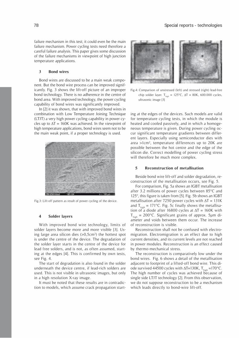
Lift-off pattern as result of power cycling of the device.Fig.3:
Comparison of unstressed (left) and stressed (right) lead-free Fig.4:
chip solder layer. Thigh
= 125°C, ∆T = 80K, 600.000 cycles,
ultrasonic image [3]
failure mechanism in this test; it could even be the main failure mechanism. Power cycling tests need therefore a careful failure analysis. This paper gives some discussion of the failure mechanisms in viewpoint of high junction temperature applications.
Bond wires3
Bond wires are discussed to be a main weak compo-nent. But the bond wire process can be improved signif-icantly. Fig. 3 shows the lift-off picture of an improper bond technology. There is no adherence in the centre of bond area. With improved technology, the power cycling capability of bond wires was significantly improved.
In [2] it was shown, that with improved bond wires in combination with Low Temperature Joining Technique (LTJT) a very high power cycling capability in power cy-cles up to ∆T = 160K was achieved. In the viewpoint of high temperature applications, bond wires seem not to be the main weak point, if a proper technology is used.
Solder layers4
With improved bond wire technology, limits of solder layers become more and more visible [3]. Us-ing large area silicon dies (>0,5cm²) the hottest spot is under the centre of the device. The degradation of the solder layer starts in the centre of the device for lead free solders, and is not, as often assumed, start-ing at the edges [4]. This is confirmed by own tests, see Fig. 4.
The start of degradation is also found in the solder underneath the device centre, if lead-rich solders are used. This is not visible in ultrasonic images, but only in a high resolution X-ray image.
It must be noted that these results are in contradic-tion to models, which assume crack propagation start-
ing at the edges of the devices. Such models are valid for temperature cycling tests, in which the module is heated and cooled passively, and in which a homoge-neous temperature is given. During power cycling oc-cur significant temperature gradients between differ-ent layers. Especially using semiconductor dies with area >1cm², temperature differences up to 20K are possible between the hot centre and the edge of the silicon die. Correct modelling of power cycling stress will therefore be much more complex.
Reconstruction of metallisation5
Beside bond wire lift-off and solder degradation, re-construction of the metallisation occurs, see Fig. 5.
For comparison, Fig. 5a shows an IGBT metallisation after 3.2 millions of power cycles between 85°C and 125°, this figure is taken from [5]. Fig. 5b shows an IGBT metallisation after 7250 power cycles with ∆T = 131K and T
high = 171°C. Fig. 5c finally shows the metallisa-
tion of a diode after 16800 cycles at ∆T = 160K with T
high = 200°C. Significant grains of approx. 5µm di-
ameter and voids between them occur. The increase of reconstruction is visible.
Reconstruction shall not be confused with electro-migration. Electromigration is an effect due to high current densities, and its current levels are not reached in power modules. Reconstruction is an effect caused by thermo-mechanical stress.
The reconstruction is comparatively low under the bond wires. Fig. 6 shows a detail of the metallisation adjacent to footprint of a lifted-off bond wire. This di-ode survived 44500 cycles with ∆T=130K, T
high =170°C.
The high number of cycles was achieved because of single side LTJT technology [2]. From this observation, we do not suppose reconstruction to be a mechanism which leads directly to bond-wire lift-off.
78 Special reports - technologies

Increase of contact reconstruction with increasing Fig.5: ∆T at
power cycling. Fig. 5a taken from [5]
a
b
c
Region adjacent to footprint of a lifted-off bond wire. Diode, Fig.6:
failed after ca. 44500 cycles
Measurement of specific resistivity Fig.7: according to the method
of van der PauwBut reconstruction increases the specific resistivity of the metallisation. It can be measured according to the method of van der Pauw [6], see Fig. 7. For sym-metrical shape of sample and symmetrical arrange-ment of contacts holds
V dln 2 Iπ
ρ = ⋅ ⋅ (2)
In this equation d is the metallisation thickness. This method can be used if the resistivity of the layer is much smaller than the resistivity of the layers below.
For the example of Fig. 5c, which is a diode, a spe-cific resistance of 0.0456 m.m was measured. At an unstressed diode of the same type, 0.0321 m.m was found. This is close to the literature value for pure Al of 0.0266 m.m. The slightly higher value is to ex-pect because the chip metallisation contains some small admixture of Si.
As result, a resistivity increase of 41% for a metalli-sation with strong reconstruction was found. This will be only of a very low effect to the forward voltage drop. During the power cycling tests of the devices in Fig. 5c and Fig. 6, only a very small increase of the diode
forward voltage drop VF in the range of 20-30mV was
observed [2]. Nevertheless, the effect of reconstruction must be regarded and further investigated, because it might affect the current distribution under high stress conditions. This might be of negative influence e.g. on the surge current capability of freewheeling diodes, but this must be further investigated.
Conclusion6
With improved bond wire technology, limits of sol-der layers become more and more visible. Beside cracks propagating from the centre to the edge, also fatigue of the solder layers starting from the centre of the devic-es is found.
Special reports - technologies 79

Under condition of improved bond wire technology, solder layers become the main weak point in the view-point of high temperature environment. Additional, with increasing junction temperature a strong reconstruction of the die metallisation layers occurs. The metallisation be-low the bond wire is less affected, but the resistivity of the metallisation is increasing significantly.
Acknowledgement7
T. Herrmann (Ferchau Engineering Schweinfurt), R. Bayerer (Infineon Technologies Warstein) and R. Amro (Palestine Polytechnic University, Hebron) are acknowl-edged for contribution to this work.
References8
Lutz, J.[1] : power Devices - future trenDs, future re-quireMents. EPE Journal Vol. 16 no 2 May 2006.
Amro, R.; Lutz, J.; Rudzki, J.; Sittig, R.; Thoben, M.[2] : power cycling at high teMperature swings of MoD-ules with low teMperature Joining technique. Pro-ceedings of the ISPSD 2006, Naples, Italy.
Herrmann, T.; Feller, M.; Lutz, J.; Bayerer, R.; Licht, [3] T.: power cycling inDuceD failure MechanisMs in sol-Der layers. Proceedings EPE 2007, Aalborg.
Morozumi, A.; Yamada, K.; Miyasaka, T.[4] : reliaBility Design technology for power seMiconDuctor MoDules. FUJI ELECTRIC JOURNAL 2001 Vol. 74 No.2.
Ciappa, M.[5] : selecteD failure MechanisMs of MoDern power MoDules. Microelectronics Reliability Vol. 42, 653-667 (2002).
Pfüller, S.[6] : halBleiter Messtechnik. VEB Verlag Tech-nik, Berlin1976, S. 89.
80 Special reports - technologies

Non-conformal seed layer deposition by PVD in narrow dual-Fig.1:
damascene structures.
Vapor pressure data of [(Fig.2: nBu3P)
2Cu(acac)] compared to other
Cu pre cursors.
Introduction1
With physical vapor deposition (PVD) being the meth-od of choice to deposit Cu seed layers required for electro-chemical Cu filling (ECD) of damascene interconnect struc-tures in ultra-large scale integrated circuits (ULSI), obstacles
are being experienced with respect to step coverage and film conformality in nanoscale trenches of high aspect ratio, Fig. 1. Taking into account that for dual-damascene struc-tures of future ULSI devices aspect ratios of 4 to 5 along with a trench width of 15 to 20 nm are expected [1], alter-native metallization techniques are highly desirable.
As a possible option for growing Cu seed layers atom-ic layer deposition (ALD) is therefore under consideration [1, 2]. Nonetheless, the growth of ultra-thin Cu films by ALD is not straight-forward, because suitable ways of re-ducing the metal precursor while avoiding too high tem-peratures that would lead to agglomeration of the films
have to be found. While several plasma-enhanced (PEALD) methods to deposit metallic Cu have been reported [3-5], pure thermal ALD is of note as it avoids drawbacks related to PEALD such as non-conformality in demanding geom-etries. To overcome the issues associated with direct, low-temperature thermal ALD, two-step processes have been proposed where copper oxide films are grown by ALD and subsequently reduced [6-8].
The current work therefore is considered with thermal ALD from [(nBu
3P)
2Cu(acac)] and wet O
2 for growing oxid-
ic Cu films on tantalum-based diffusion barriers as well as on ruthenium and silica. The Cu(I) precursor used in this study is of particular interest as it is a liquid at room tem-perature and thus easier to handle than frequently utilized solids such as [Cu(acac)
2], [Cu(hfac)
2] or [Cu(thd)
2]. Further-
more the substance is non-fluorinated which helps avoid-ing a major source of adhesion issues repeatedly observed in Cu CVD.
Experimental2
The precursor [(nBu3P)
2Cu(acac)] was synthesized by stan-
dard Schlenk techniques according to published methods [9, 10]. Vapor pressure measurements, Fig. 2 display that the volatility of the substance is comparable to [Cu(acac)
2], but
Thomas Waechtler1, Nina Roth2, Steffen Oswald3, Stefan E. Schulz1,4, Heinrich Lang2, Thomas Gessner1,4
1Center for Microtechnologies, Faculty for Electrical Engineering
and Information Technologies, Chemnitz University of Technology,
Chemnitz, Germany 2 Institute of Chemistry, Chemnitz University of Technology,
Chemnitz, Germany 3Leibniz Institute for Solid-State and Materials Research (IFW),
Germany 4Fraunhofer IZM Chemnitz Branch, Chemnitz, Germany
ALD of Copper and Copper Oxide Thin Films for Applications in ULSI Metallization Systems
Special reports - technologies 81
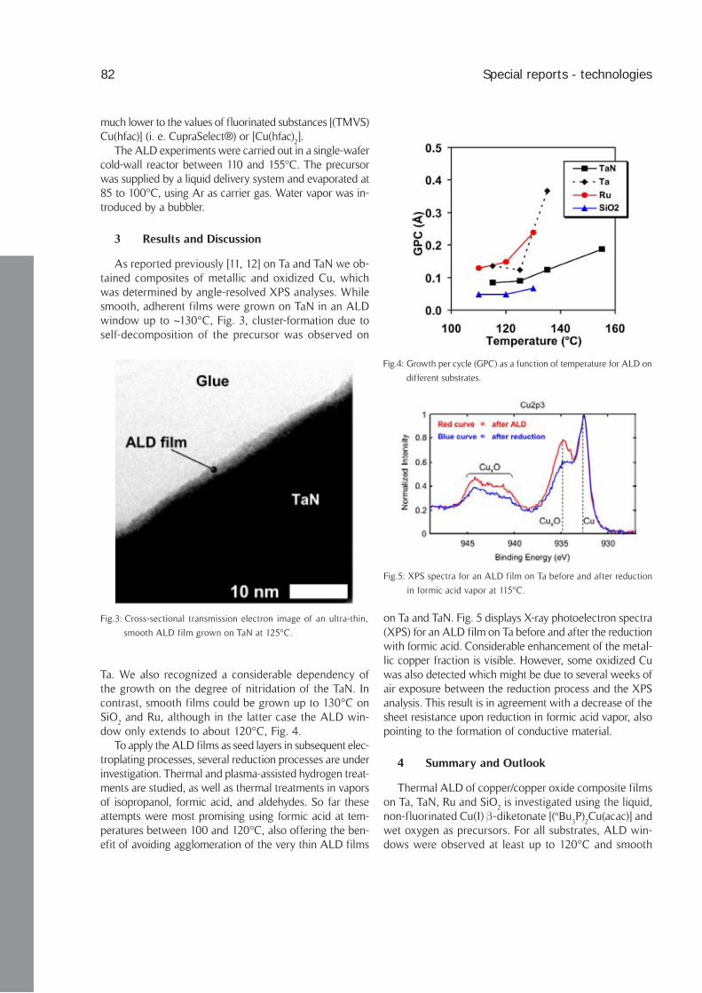
Cross-sectional transmission electron image of an ultra-thin, Fig.3:
smooth ALD film grown on TaN at 125°C.
Growth per cycle (GPC) as a function of temperature for ALD on Fig.4:
different substrates.
XPS spectra for an ALD film on Ta before and after reduction Fig.5:
in formic acid vapor at 115°C.
much lower to the values of fluorinated substances [(TMVS)Cu(hfac)] (i. e. CupraSelect®) or [Cu(hfac)
2].
The ALD experiments were carried out in a single-wafer cold-wall reactor between 110 and 155°C. The precursor was supplied by a liquid delivery system and evaporated at 85 to 100°C, using Ar as carrier gas. Water vapor was in-troduced by a bubbler.
Results and Discussion3
As reported previously [11, 12] on Ta and TaN we ob-tained composites of metallic and oxidized Cu, which was determined by angle-resolved XPS analyses. While smooth, adherent films were grown on TaN in an ALD window up to ~130°C, Fig. 3, cluster-formation due to self-decomposition of the precursor was observed on
Ta. We also recognized a considerable dependency of the growth on the degree of nitridation of the TaN. In contrast, smooth films could be grown up to 130°C on SiO
2 and Ru, although in the latter case the ALD win-
dow only extends to about 120°C, Fig. 4.To apply the ALD films as seed layers in subsequent elec-
troplating processes, several reduction processes are under investigation. Thermal and plasma-assisted hydrogen treat-ments are studied, as well as thermal treatments in vapors of isopropanol, formic acid, and aldehydes. So far these attempts were most promising using formic acid at tem-peratures between 100 and 120°C, also offering the ben-efit of avoiding agglomeration of the very thin ALD films
on Ta and TaN. Fig. 5 displays X-ray photoelectron spectra (XPS) for an ALD film on Ta before and after the reduction with formic acid. Considerable enhancement of the metal-lic copper fraction is visible. However, some oxidized Cu was also detected which might be due to several weeks of air exposure between the reduction process and the XPS analysis. This result is in agreement with a decrease of the sheet resistance upon reduction in formic acid vapor, also pointing to the formation of conductive material.
Summary and Outlook4
Thermal ALD of copper/copper oxide composite films on Ta, TaN, Ru and SiO
2 is investigated using the liquid,
non-fluorinated Cu(I) b-diketonate [(nBu3P)
2Cu(acac)] and
wet oxygen as precursors. For all substrates, ALD win-dows were observed at least up to 120°C and smooth
82 Special reports - technologies

films could be obtained. On Ta, however, and at elevated temperature also on TaN, cluster formation was observed along with an increase of the GPC due to apparent self-decomposition of the precursor in a CVD-like manner.
For possible applications of the ALD films as seed layers in electrochemical Cu damascene metallization schemes, the films are subjected to reduction processes. So far treatments in formic acid vapor appear most prom-ising. Reduction of films on Ta was already observed at 115°C, hence in the same temperature range as the ALD processes, which helps avoid agglomeration of the films otherwise observed at higher temperature.
Further work will concentrate on optimizing both the ALD and the reduction processes, as well as on applying the ALD films as seed layers for Cu ECD.
Acknowledgements5
We thank Dr. A. Siddiqi (Univ. Duisburg-Essen) for vapor pressure measurements as well as Dr. S. Schulze and A. Moskvinova (TU Chemnitz) for TEM analyses. Funding obtained from the German Research Founda-tion (DFG) in the International Research Training Group 1215 “Materials and Concepts for Advanced Intercon-nects” is gratefully acknowledged.
References6
SIA et al. (Ed.)[1] : the international technology roaD-Map for seMiconDuctors (itrs). 2005 Edition and 2006 Update (http://www.itrs.net).
Kim, H.[2] : atoMic layer Deposition of Metal anD ni-triDe thin filM: current research efforts anD appli-cations for seMiconDuctor Device processing. Vac, J. Sci. Technol. B 21 (6), 2231 (2003).
Niskanen, A.; Rahtu, A.; Sajavaara, T.; Arstila, K.; [3] Ritala, M.; Leskelä, M.: raDical-enhanceD atoMic layer Deposition of Metallic copper thin filMs. J. Electrochem. Soc. 152 (1), G25 (2005).
Jezewski, C. Lanford, W.A.; Wiegand, C.J.; Singh, [4] J.P.; Wang, P.-I.; Senkevich, J.J.; Lu, T.-M.: inDuc-tively coupleD hyDrogen plasMa-assistenD cu alD on Metallic anD Dielectric surfaces. J. Electrochem. Soc. 152 (2), C60 (2005).
Wu, L.; Eisenbraun, E.[5] : hyDrogen plasMa-enhanceD atoMic layer Deposition of copper thin filMs. J. Vac. Sci. Technol. B 25 (6), 2581 (2007).
Huo, J. ; Solanki, R.; McAndrew, J.[6] : characteristics of copper filMs proDuceD via atoMic layer Deposition. J. Mater. Res. 17 (9), 2394 (2002).
Lee, C.; Lee, H.-H.[7] :a potential novel two-step MocvD of copper seeD layers. Electrochem. Sol-id-State Lett. 8 (1), G5 (2005).
Kim, H.; Kojima, Y.; Sato, H.; Yoshii, N.; Hosaka, S.; [8] Shimogaki, Y.: thin anD sMooth cu seeD layer De-position using the reDuction of low teMperature De-positeD cu
2o. MRS Symp. Proc. 914, 167 (2006).
Shin, H.-K.; Hampden-Smith, M. J.; Duesler, E. N.; Ko-[9] das, T.T.: the cheMistry of copper(i) b-Diketonate coM-pounDs - part v. Can. J. Chem. 70, 2954 (1992)
Shen, Y.-Z.; Leschke, M.; Schulz, S. E.; Ecke, R.; [10] Gessner, T.; Lang, H.: synthesis of tri-n-Butylphos-phine copper(i) Beta-Diketonates anD their use in chiM-ical vapour Deposition of copper. Chinese J. Inorg. Chem. 20 (11), 1257 (2004).
Waechtler, T.; Roth, N.; Oswald, S.; Schulz, S.E.; [11] Lang, H.; Gessner, T.: coMposite filMs of copper anD copper oxiDe DepositeD By alD. AVS ALD Confer-ence (2007).
Waechtler, T.; Oswald, S.; Pohlers, A.; Schulze, S.; [12] Schulz, S.E.; Gessner, T.: copper anD copper oxiDe coMposite filMs DepositeD By alD on tantaluM-BaseD Diffusion Barriers. Advanced Metallization Confer-ence (AMC) (2007).
Special reports - technologies 83

“mask” approach: a) after CMP and “wet-etch-mask” pattern-Fig.1:
ing; b) and c) partially wet etched by buffered HF; d) fully re-
moved USG dielectrics, encapsulated airgap structures (using
non-conformal CVD)
“spacer” approach: a) after CMP and “wet-etch-mask” pattern-Fig.2:
ing; b) and c) partially wet etched by buffered HF; d) fully re-
moved USG dielectrics, encapsulated airgap structures (using
non-conformal CVD)
Introduction1
The formation of airgap structures is a promising al-ternative to achieve low-k or even ULK performance for future technology nodes. It has been shown that k
eff - val-
ues of 2.5 or even significantly lower are well achievable for different integration schemes and MPU generations [1],[2],[3]. Beyond this, several Airgap approaches largely share conventional processing of Cu and SiO
2.
Two similar sacrificial layer airgap approaches (“mask” and “spacer”) were developed at TU Chemnitz. The fea-sibility of both variants was shown [4] and characterized in terms of their electrical properties (reduction of in-ter-metal capacitances and k
eff) [1]. The general process
flows of both approaches is shown in Fig. 1 (“mask”) and Fig. 2(“spacer”). The removal of the sacrificial PECVD SiO
2
is performed by buffered HF solution (airgap formation). The application of a wet etch treatment is one of the ma-jor routes of sacrificial airgap formation known from the
literature. The metal lines (Cu) and the dielectric barriers align the wet etch treatment. The functional films for etch stop and masking of both airgap approaches consist of PECVD SiC:H. Critical processes in terms of the reliability of airgap formation were discussed in [5]. The formation of cavities for the “spacer” approach occurs semi-self aligned at the sidewall of the interconnect lines (due to the spacer material, see Fig. 2 b). Because of this mechanism a more relaxed patterning of the wet etch mask can be used and SiO
2 remains in the case of large interconnect spacing and
provide mechanical support, compare Fig. 1 and Fig. 2.This contribution is related to the impact of wet etch
media (HF acid) on dielectric and conductive diffusion bar-rier materials and on Cu interconnect lines, respectively. The exami-nations included blanked film tests and tests on patterned structures.
Experiment2
Blanket film tests: Electrical measurements of sheet resistance (Rs) during exposure to HF wet etch media (up to approximately 5 min) were performed for 30 nm films of PVD TaN
X, PVD TiN
X, CVD WN
X and 500 nm
films of MOCVD Cu und PVD Cu. The measurements were arranged by the tool Ominmap Rs 50/e (LOT Oriel). Different concentrations of the acid (buffered HF, HF
40%/
H2O (2/1), HF
40%) and temperatures (20 °C, 40 °C) of wet
Knut Schulze, Stefan E. Schulz, Thomas Gessner
Center for Microtechnologies, Faculty for Electrical Engineering
and Information Technologies, Chemnitz University of Technology,
Chemnitz, Germany
Evaluation of Airgap structures produced by wet etch of sacrificial dielectrics: Impact of wet etch media on diffusion barriers and copper
84 Special reports - technologies

Schematical preparation of the “closeness-test” of conductive Fig.3:
diffusion barrier films under exposure of HF acid
SEM cross-section image of real preparation according to Fig.3 c)Fig.4:
Dependency of Fig.5: Rs on exposure time to HF wet etch media to the
refractive metal nitrides PVD TiNX, PVD TaN
X and CVD WN
X
etch solution were used for the examinations. Moreover the behaviour of the surface of these materials under HF impact was examined by SEM images and AFM profiles (AFM tool: D3000, Digital Instruments).
Patterned structure tests: The conductive barrier films protect the sidewalls of the copper lines against the impact of HF dilution - if they are totally tight, see Fig. 1 b, c and Fig. 2 b, c. A special technique was de-veloped to examine the closeness of conductive barrier films under HF exposure. This test includes an HF at-tack from the deposition side which matches the condi-tions of the real airgap preparations, according to Fig. 1 and Fig. 2. This technology is schematically shown in
Fig. 3. The conductive barrier materials surround areas of SiO
2 which are undamaged if the diffusion barriers
are totally tight against HF media, see Fig. 3 d. In con-trast to this HF dilution etches SiO
2 in the encapsulated
regions if any defect allows penetration through the con-ductive barrier films. The “closeness-test” was investigat-ed for different barrier films, varied thicknesses and HF
treatment times as well as on vertically and horizontally oriented films. A SEM image of preparations is shown in Fig. 4. The investigations focused on MOCVD TiN
X,
PVD TiNX, CVD WN
X and PVD TaN
X of 10 nm as well
as 20 nm thicknesses. The exposure times of each film were 2 min up to 15 min.
Discussion3
Blanket film tests: All conductive diffusion barri-er films show increasing Rs with exposure time to HF wet etch media, see Fig. 5. The highest slope occurs for the first 10 s of the treatment at all samples. The sub-sequent HF treatment affects a leads to a linear slope
for all samples. The varied HF concentrations as well as both temperatures (20 °C, 40 °C) have different impacts depending on the films. The PVD TiN
X is more sensi-
tive to higher HF concentration (up to 26 % change in Rs). Moreover it shows the highest sensitivity com-pared to PVD TaN
X and CVD WN
X. The influence of a
temperature variation is not clear and differs. The PVD TaN
X layer is almost unaffected by buffered HF at room
temperature. This is possibly due to the formation of a selfpassivating film. PVD TiN
X and PVD TaN
X show the
lowest damage by buffered HF in comparison to higher concentrations. In contrast to this CVD WN
X showed the
strongest modification for buffered HF, but it was only slightly damaged by highly concentrated HF
40% and all
Special reports - technologies 85

Dependency of Fig.6: Rs on exposure time of HF wet etch media
to MOCVD and PVD copper films
Comparison of RRMS-values of PVD TiNx, CVD WNx, PVD Fig.7:
TaNx, MOCVD Cu and PVD Cu immediately after deposition
and after exposure to buffered HF for 5 minutes
AFM images of MOCVD Cu: a) after deposition; b) after expo-Fig.8:
sure to buffered HF for 5 minutes
Statistical results of the “closeness-test” for the conductive dif-Fig.9:
fusion barrier films MOCVD TiNX, PVD TiN
X, CVD WN
X and
PVD TaNX with thicknesses of 10 nm and 20 nm
ygen (O2) causes a significant oxidation rate of the bar-
rier film. This mechanism is superposed by the wet etch of oxidized metal films by HF. Higher temperatures of the etch solutions reduce the ability of oxygen dissolv-ing. This would definitely reduce the impact of the wet treatment and appears logical since a temperature vari-ation showed different on the behaviour of Rs. The im-pact of buffered HF @ 20 °C on Rs values correlates very well to the RMS values of Fig. 7. There is a negligibly low increase of RMS for the PVD TaN
X, but a significant
change in the case of PVD TiNX as well as CVD WN
X
films. The copper films show a behaviour similar to the conductive barrier films, see Fig. 6. Diluted HF media induces corrosion [6] (oxidation) of Cu films (in contrast to this, ammonium peroxide mixture (APM, K1) causes passivation of copper films (formation of Cu(OH)
2). HF
media etches metal oxides simultaneously and reduc-es the film thickness. First of all an attack at the grain boundaries occurs. The average grain sizes of both films are comparable (both about 220 nm). The PVD Cu is (111) oriented, MOCVD Cu mainly (111) and (100). These morphological distinctions and impurities of both copper films are probably responsible for the different impact of HF media. The RRMS measurements of both copper films, see Fig. 8, show only a slight change under buff-ered HF exposure. This is also confirmed by comparable AFM profiles before and after wet treatment, see Fig. 8 for MOCVD Cu images.
Patterned structures tests: Fig. 9 shows the statisti-cal analysis of the “closeness-tests” for different conduc-tive barriers and varied thickness. It was observed that exposure times up to 4 min cause generally no chemi-cal breakthrough of buffered HF even for very low film thicknesses of 10 nm, see Fig. 10 a. The most promising
dilutions at 40 °C. The mechanisms for the Rs increase were not further proven. It is assumed that the wet etch attack occurs primarily at the grain boundaries, followed by a homogeneous thickness reduction. This would also justify the reduced impact for the amorphous CVD WN
X film. Furthermore it is expected that dissolved ox-
86 Special reports - technologies
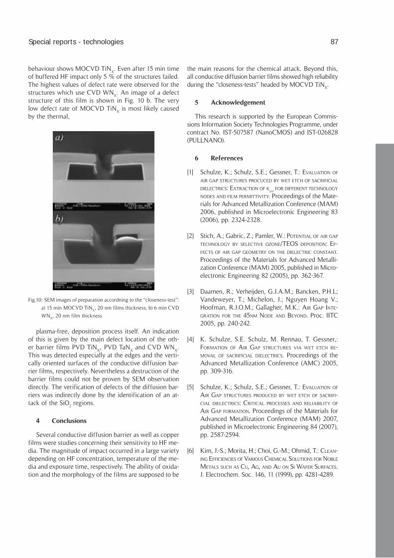
SEM images of preparation accordning to the “closeness-test”: Fig.10:
a) 15 min MOCVD TiNX, 20 nm films thickness; b) 6 min CVD
WNX, 20 nm film thickness
behaviour shows MOCVD TiNX. Even after 15 min time
of buffered HF impact only 5 % of the structures failed. The highest values of defect rate were observed for the structures which use CVD WN
X. An image of a defect
structure of this film is shown in Fig. 10 b. The very low defect rate of MOCVD TiN
X is most likely caused
by the thermal,
plasma-free, deposition process itself. An indication of this is given by the main defect location of the oth-er barrier films PVD TiN
X, PVD TaN
X and CVD WN
X.
This was detected especially at the edges and the verti-cally oriented surfaces of the conductive diffusion bar-rier films, respectively. Nevertheless a destruction of the barrier films could not be proven by SEM observation directly. The verification of defects of the diffusion bar-riers was indirectly done by the identification of an at-tack of the SiO
2 regions.
Conclusions4
Several conductive diffusion barrier as well as copper films were studies concerning their sensitivity to HF me-dia. The magnitude of impact occurred in a large variety depending on HF concentration, temperature of the me-dia and exposure time, respectively. The ability of oxida-tion and the morphology of the films are supposed to be
the main reasons for the chemical attack. Beyond this, all conductive diffusion barrier films showed high reliability during the “closeness-tests” headed by MOCVD TiN
X.
Acknowledgement5
This research is supported by the European Commis-sions Information Society Technologies Programme, under contract No. IST-507587 (NanoCMOS) and IST-026828 (PULLNANO).
References6
Schulze, K.; Schulz, S.E.; Gessner, T.[1] : evaluation of air gap structures procuceD By wet etch of sacrificial Dielectrics: extraction of k
eff for Different technology
noDes anD filM perMittivity. Proceedings of the Mate-rials for Advanced Metallization Conference (MAM) 2006, published in Microelectronic Engineering 83 (2006), pp. 2324-2328.
Stich, A.; Gabric, Z.; Pamler, W.[2] : potential of air gap technology By selective ozone/teos Deposition: ef-fects of air gap geoMetry on the Dielectric constant. Proceedings of the Materials for Advanced Metalli-zation Conference (MAM) 2005, published in Micro-electronic Engineering 82 (2005), pp. 362-367.
Daamen, R.; Verheijden, G.J.A.M.; Bancken, P.H.L; [3] Vandeweyer, T.; Michelon, J.; Nguyen Hoang V.; Hoofman, R.J.O.M.; Gallagher, M.K.: air gap inte-gration for the 45nM noDe anD BeyonD. Proc. IITC 2005, pp. 240-242.
K. Schulze, S.E. Schulz, M. Rennau, T. Gessner,[4] : forMation of air gap structures via wet etch re-Moval of sacrificial Dielectrics. Proceedings of the Advanced Metallization Conference (AMC) 2005, pp. 309-316.
Schulze, K.; Schulz, S.E.; Gessner, T.[5] : evaluation of air gap structures proDuceD By wet etch of sacrifi-cial Dielectrics: critical processes anD reliaBility of air gap forMation. Proceedings of the Materials for Advanced Metallization Conference (MAM) 2007, published in Microelectronic Engineering 84 (2007), pp. 2587-2594.
Kim, J.-S.; Morita, H.; Choi, G.-M.; Ohmid, T.[6] : clean-ing efficiencies of various cheMical solutions for noBle Metals such as cu, ag, anD au on si wafer surfaces. J. Electrochem. Soc. 146, 11 (1999), pp. 4281-4289.
Special reports - technologies 87

SEM cross section view of the smaller via entrance because of Fig.1:
the etch profile and higher step coverage of deposition processes
in the upper part in TSVs; leads to via entrance closing without
complete fill in via (isolation, CVD-TiN/Cu-CVD)
Ramona Ecke1; Lutz Hofmann1; Matthias Kuechler2; Stefan E. Schulz2
1 Center for Microtechnologies, Faculty for Electrical Engineering
and Information Technologies,Chemnitz University of Technology,
Chemnitz, Germany 2Fraunhofer IZM Chemnitz Branch, Chemnitz, Germany
Through Silicon Forming and Metallization for 3D Integration
Introduction1
Three-dimensional (3D) interconnects by through hole vias (TSV) are one solution for overcoming the increase of delay and power limitations of on-chip 2D interconnects. The directly stacked die interconnec-tions reduce line length, chip size and especially cost. In addition, the 3D integration has the opportunity for hetero-integration, to provide diverse functionally so-lutions to consumer requirements. Hetero-integration can combine the advantages of different device tech-nologies, such us logic, analog, memory and MEMS, based on incompatible process flows, to fabricate new compact systems. [1]
According to the application of the multi-layered 3D system and therefore combinations of different devic-es, there exist diverse 3D integration schemes. One of the key roles in 3D chip stacking plays the fabrication and metallization of Through Silicon Vias (TSV) used to electrically connect the dies.
Experimental and results2
TSV-Etch2.1
The TSV forming is carried out in 3 steps, etching, passivation and metallization. We are focused on the void free filling of TSVs by chemical vapor deposition (CVD) for metallization. The first crucial condition for TSV filling is the TSV profil after etching.
TSV’s are made by deep reactive ion etching (DRIE). This is one of the most critical steps regarding cost and throughput constraints because of high depth (50-150 µm) and partially high density of TSV’s. The etch process it-self should offer high etch rates, smooth sidewalls, con-trollable sidewall angle and small mask undercut. Con-
ventional deep Si etching leads to vias with a straight entrance or even with an overhang at the top. For fill-ing of TSV’s by deposition of isolation layer, barrier layer and copper this means a pinch-off of the copper film at the via top and a void formation at the lower part of the vias. Better suited are completely V-shaped vias, which is difficult to realize for very deep vias, or at least V-shaped via entrances.
We fabricated TSV’s by DRIE with a modified Bosch process in a STS etching tool. To obtain a tapered open-ing at the via-top a 4- to 8-step etching process recipe was chosen with a mixture of isotropic and anisotro-pic etching, Fig. 2. The first step is of isotropic nature with a low bias power and a relative high cycle time, that is reduced cycle by cycle to taper the via-opening. This means lowering of the ratio of etch time to pas-sivation time by each etch cycle. Step 2 is of anisotro-pic character with a much higher bias power and much lower cycle time. In step 3 the bias power as well as the number of cycles is increased continuously until a certain value is reached which is then held constant in etch step 4. Such a sequence, for which the bias pow-
88 Special reports - technologies

Sketch of the etch sequence (a) and etch power as well as number of cycles versus etch time (b)Fig.2:
Development steps of the tapered via opening a) one isostropic cycle and b) 4.5 isotropic cycle with decreasing cycle time in step one Fig.3:
of the etching process
er and cycle times are principally shown in Fig. 2b, is used for etch depths up to 50 µm. For higher depths the sequence is extended up to 8 steps repeating step 3 and step 4.
With the etch process described above we obtained a well tapered via entrance. Fig. 3 depicts the profiles of via openings with the multistep process. The figure on the left shows the result of a process which uses one single isotropic etch cycle in etch step one. One can see that there is an undercut of the etch mask and so a wider opening compared to via etched in a con-ventional process. If the number of etch cycles in step 1 is increased to 4-6 and at the same time cycle time is reduced cycle by cycle the resulting etch profile is as shown in Fig. 3b. The reduction of cycle time leads to a more anisotropic etch and thus the via-opening gets tapered by every cycle. The angle between via wall and the top surface is 80 degree in this case. The surface of the via is slightly waved due to the etch cycles. That effect can be minimized by choosing a highly confor-
mal deposition method (e.g. using TEOS/Ozon chem-istry) for the subsequent insulating film.
Barrier deposition2.2
The required metallization of TSV’s needs to be de-posited after the electrical isolation in such a way, that reliable electrical interconnects are formed. Mostly the TSV metallization consists of a bi- or multilayer stack of a thin diffusion barrier, adhesion layer and/or seed layer and the conductor material copper. We use CVD pro-cesses for barrier and copper deposition especially with regard to the high step coverage of these processes also in high aspect ratio structures (AR > 5).
Currently TiN by CVD is the most promising barri-er material for application in 3D integration concerning precursor availability, deposition temperature (< 400°C), good conformality and barrier properties. The TiN bar-rier layers are produced by a multistep process consist-ing of alternating pyrolysis steps from TDMAT as pre-
Special reports - technologies 89

TiN coverage in TSV in dependence of their diameters, with Fig.4:
larger diameter better coverage
Overview of deposition processes and concepts for metallization of TSVsFig.5:
regime. Reducing the deposition temperature leads also to a better step coverage however the deposition rate is drastically reduced. For very high aspect ratios (e.g. ~20) the pressure should be also reduced for a void free filling. The reaction byproducts of copper CVD have low volatility, so it is impeded to remove the reaction byproducts from the lower part of TSV’s. This reduc-es the step coverage and leads to void formation due to the faster closure of the upper part of TSV. The step coverage of copper should be more than 90% to avoid the void formation in a complete copper CVD fill.
Copper deposition by CVD2.3
In general different deposition techniques are avail-able to realize metal deposition: physical vapor deposi-tion (PVD), electrochemical deposition (ECD, electroplat-ing) or electroless plating and chemical vapor deposition (CVD). Apart from PVD all processes are able to fill high aspect ratio patterns. Figure 5 shows the applicability of different deposition processes and filling concepts de-pending on the TSV diameter. The pure metal CVD ap-proach is suited for complete TSV fill with lateral width of up to ~3 µm at high aspect ratios. It is currently not clear to which extend the electroplating technology is able to substitute MOCVD (metal-organic chemical va-por deposition) processes for high aspect ratio (HAR) TSV metallization [2, 3]. However, if aspect ratios of larger than 7:1 are to be filled with a conducting mate-rial, CVD is the process with the highest currently avail-able conformality. In the region above 3 µm lateral size, several factors impede the application of copper CVD, like process limitations for Cu CVD. In this case, filling can be performed by electroplating. CVD can be used to deposit a so-called seed layer only, which then acts
cursor and plasma treatment steps for densifying. The step coverage in high aspect ratio TSV depends strong-ly on their geometry and diameter size as well as their depth. With larger diameter the step coverage is im-proved. In Fig. 4 the step coverage of TiN, deposited with standard conditions, is shown in dependence of TSV diameter.
We counteracted the reduced step coverage in small-er TSV diameter and higher aspect ratios with decreas-ing of deposition temperature and extension of the py-rolysis step time.
The step coverage of the TiN barrier depends strongly of via geometry and depth. With the standard process (420°C and pyrolysis step time 5s) the sidewalls of the TSV are covered by the barrier only up to a depth of 4 (ratio opening to depth). If the TSVs are deeper the lower part of the TSV is not covered by TiN. The stan-dard conditions of the process are closed to the trans-port-controlled regime. With lowering the deposition temperature and increasing the step time of pyrolysis steps the precursor mol-ecules get the chance to reach the via bottom and deposit there. The pyroly-sis step time should be op-timized for each TSV diam-eter and depth. In this way a step coverage around 50% at the bottom can be cer-tainly obtained also in as-pect ratios > 10.
As well as for the TiN de-position the standard cop-per CVD process is close to the transport controlled
90 Special reports - technologies

Influence of deposition pressure on coverage in TSV with very high aspect ratio > 20Fig.6:
as a base layer to grow metals by following electroplat-ing techniques. This is especially of great interest since even most advanced PVD tools are hardly able to cover vias with aspect ratios larger than 7:1 [4, 5].
Depending on the chosen metallization scheme, a thin conducting CVD layer such as Barrier/Cu can be used as a seed layer for the subsequent electroplating process.
The deposition equipment used was a P5000 with a lamp-heated Blanket Tungsten Chamber. The results
described in this chapter were obtained with the pre-cursor (hfac)Cu(TMVS) which is evaporated using a liquid delivery system (LDS). This system is composed of a liquid flow meter for the precursor, a mass-flow controller for the carrier gas and a controlled evap-orator unit from Bronkhorst. Within the system the precursor is dosed as a liquid with high accuracy and is vaporised just before the deposition. The copper CVD is used for complete fill of smaller TSVs < 3µm diameter and for deposition of seed layer for fill by electroplating.
With copper CVD we obtain very high step cover-age of nearly 100% what is account of the deposition rate. This limits the application of copper CVD, on one side for complete fill in small TSV structures < 3 µm or on the other side for the deposit a highly confor-mal seed layer for further electroplating fill.
Summary3
The formation of the Through Silicon Vias (TSV) as electrical contact is a very important step in the 3D in-tegration and includes the TSV deep etch and metalli-zation. The formed via profile during the etch process influences the further deposition processes for met-allization. The TSV’s need a tapered profile for void free filling. However this is difficult to realize in such
deep structures with high aspect ratios. So we use a modified etch process for adapted via geometry at the entrance of TSV. This ta-pered via entrance profile avoids an early closure of TSV before void free filling.
The step coverage of the CVD processes for TiN barrier and Cu were optimized. Lower deposition temperatures lead to film with high-er conformality. For the Cu CVD beside the decrease of tempera-ture also the reduction of cham-ber pressure strongly influences the conformality. Nevertheless the pro-cesses have to be adjusted for each TSV geometry and layout with re-spect to the size, depth and den-sity of TSV’s.
References4
Tsang, C.K.;. Andry, P.S et al.[1] : proceeDings of Mat-er. Res. Soc. Symp., 970 (2007).
Bioh Kim, in[2] : 2006 Mrs syMposiuM proceeDings, voluMe 970, 0970-y06-02, 253 (2007).
Burkett, S.; Schaper, L. et al, in[3] : 2006 Mrs syM-posiuM proceeDings, voluMe 970, 0970-y06-01, 261 (2007).
Wang, Shi-Qing et al, in[4] : J. Vac. Sci. Technol. Vol. 14, Issue 3, 1846 (1996).
Rossnagel, S.M.; Kim, H., in[5] : 2001 proceeDings iitc, 3-5 (2001).
Special reports - technologies 91
Sascha Hermann1, Stefan Schulz1,2, Thomas Gessner1,2 1 Center for Microtechnologies, Faculty for Electrical Engineering
and Information Technologies, Chemnitz University of Technology,
Chemnitz, Germany 2Fraunhofer IZM Chemnitz Branch, Department Micro Devices
and Equipment, Chemnitz, Germany
Preparation and investigation of multi wall carbon nanotubes for interconnect applications
Introduction1
Carbon Nanotubes have outstanding structural, elec-tronic and mechanical properties which open new possi-bilities for applications in NEMS or in integrated circuit devices.1 Looking on the requirements for future inte-grated circuits as listed in the ITRS CNTs are probably the most promising material achieving the challenging aims of smaller feature sizes and higher stress demands where common material systems start to fail.2 Metallic CNTs have been proposed for nanoelectronic intercon-nects as the can carry extreme current densities, are more or less insensitive to electromigration and show very good thermal conductivity.3
Despite the fact that in fundamental experiments CNTs showed remarkable results there are huge bar-riers for integration of CNTs in nanoelectronics which have to be overcome. For these and other applications reproducible and scalable production of CNT-based de-vices has to be accomplished. Furthermore these pro-duction processes have to take place at conditions com-patible with standard microelectronic process lines as for example at temperatures as low as 450°C. As we are interested in electronic interconnects we focus in this work on the direct growth of MWNTs with cat-alyst-mediated thermal chemical vapour deposition. This technique allows scalable CNT growth at rath-er low temperatures. The catalyst (Fe, Co, Ni or alloys 4,5,6, 7,8,9) defines growth sites and the growth condition of the CNTs. It was found that there is a strong corre-lation between catalyst particle size and the diameter of the CNTs. This shows the importance of controlling nanoparticle formation as this can control the proper-ties and density of CNT films.
In this work we show basic experiments on the prep-aration of nickel catalyst particles at different temper-atures, from different Ni-thicknesses and on different
substrates. The NP-topography was investigated with scanning electron microscopy. Orienting on later on ap-plication in electronic devices also silicon samples cov-ered with Al or TiN supporting layers were prepared. We prepared test structures for selective growth of CNTs out of contact holes as a first step towards integration.
The growth of MWNTs under variation of temper-ature, gas composition and pressure was performed and characterized with SEM, TEM and Raman spec-troscopy.
Experiment 2
The most experiments were performed on silicon sub-strates covered with a 200 nm thick SiO
2 layer prepared by
thermal oxidation. On top a very thin Ni film in the range of 1 to 5 nm was deposited with PVD. Aluminium layers with a thickness of 100 nm were sputtered on Si/SiO
2-sub-
strates. For selective growth of CNTs a silicon substrate with a stack of SiO
2/TiN/Cu/TiN/Ni (Fig. 6) was prepared and
structured with optical lithography and wet etching steps. The Cu layer was embedded by TiN layers acting as a bar-rier against copper diffusion and was sputtered by reactive PVD with a thickness of 50 nm. For the selective deposi-tion of the catalyst a lift-off technique was applied.
The preparation of nano-particles and the growth of CNTs was performed in a thermal CVD system. This is a cold wall HV-chamber with a graphite reactor inside es-pecially designed for CNT-growth. The sample holder can capture wafers up to 4”. The gas mixture (N
2, C
2H
4, H
2)
is spread through a showerhead over the sample. To opti-mize gasflow for homogeneous CNT-growth on the wafer finite element simulations for different reactor geometries were performed [CoNTemp -project].
Catalyst nanoparticles were prepared by annealing dif-ferent substrates at temperature ranging from 500°C to 790°C under N
2/H
2 atmosphere. After pre-treatment the
sample was rapidly cooled down to conserve the NP state at these conditions. The sample topography was charac-terized with SEM.
The MWNT samples were prepared by continuing the pre-treatment phase with introduction of ethylene (C
2H
4).
We varied temperature, gas composition and pressure and characterization was conducted with SEM, HRTEM and Raman spectroscopy.
92 Special reports - technologies

SEM plan views and size distributions of Ni nanoparticles on Fig.1:
200 nm SiO2 substrates prepared at 500°C and 790°C
NP-mean diameter and -density as function of initial layer Fig.2:
thickness of Ni catalyst at 700°C determined from HRSEM
SEM plan views of Ni nanoparticles formed on 200 nm SiOFig.3: 2
and 100nm Al at 500°C
Results3
Our investigations were first focused on the effect of different annealing temperatures, catalyst thicknesses and substrates on Ni nanoparticle (NP) formation, Fig.1-3. The metal films deposited on the interlayer SiO
2 trans-
form into nanoparticles as shown in Fig.1 for 2 nm Ni film at 500°C and 790°C. With increasing temperature the particle size distribution is changed as shown in the histograms. This process is driven by clusters diffusion which increases with annealing temperature resulting in the coalescence of neighbouring particles. As a conse-quence one gets a bigger spread in particle size distri-bution with many very small NPs but also with very big particles which are both not favourable for CNT-growth at selected growth temperatures whereas at 500°C a more or less symmetrical distribution with a mean di-ameter of 30.4 nm was observed.
Fig. 2 summarizes the SEM results of particle sizes and densities from different Ni-thicknesses. Mean particle diameter shows a linear dependence to the thickness of the starting layer. Meanwhile the density increases with decreasing thickness reaching a value of 3*1010cm-1 for
the case of 2 nm Ni film. It was observed that particle size distribution spreads strongly with thicker Ni-layers and the particles become more uneven. For CNT growth just the thinner catalyst layers are of interest as here the size distributions are much narrower and densities are the highest one. Fig.3 demonstrates NPs prepared on Al support. Obviously Al, which is covered with a thin na-tive oxide layer, effects NP formation as the size distri-bution shifts to bigger sizes when initial film thickness was 2 nm. This is attributed to lower adhesion forces be-tween Al
2O
3 and Ni. Furthermore NPs on Al show uni-
form shapes predominantly aligned at the grain bound-aries of the underling Al-film.
Fig.4 shows SEM and HRTEM observations of as-grown CNTs on SiO
2 at 500°C and 790°C. For lower
temperatures like shown for 500°C a massive growth of twisted MWNTs was achieved whereas higher temper-atures conducted to a lower growth rate due to growth kinetics and also a lower growth density but with a bet-ter crystallization.
Growth density is also determined by the size and the condition of catalyst particles before CNT growth initia-tion and can explain the low density achieved at 790°C. As shown above NP size distribution changes with tem-perature leading to a lower densities of suitable catalysts for CNT growth. This exposes a gap between the condi-tions for ideal NP formation and the conditions for CNT growth which has to be further optimized. HRTEM ob-servations as shown in Fig.4 (c, d, e) show that predomi-nantly multi walled nanotubes (MWNT) with a diameter of around 20 nm in the tip-growth mode were grown. Increasing temperature affects positively on the crystal-linity of MWNTs as seen at Fig.4e where the shell struc-ture of the MWNT could clearly been observed. Further-
Special reports - technologies 93

SEM and HRTEM of MWNTs grown at 500°C [a, c] and 790°C Fig.4:
[b, d, e] on SiO2 and a growth time of 10 min
Raman spectra from MWNTs prepared at 500°C...790°C showing Fig.5:
the characteristic D-Band (1353cm-1) and G-Band (1580 cm-1).
Fig.6: Selective growth of dense MWNTs out of 400 nm deep contact holes on Fig.6:
prestructured conductive substrates by CVD at 600°C
showed just a slight improvement in quality with in-creasing H
2 concentration. As a first step towards in-
tegration we achieved selective growth of MWNTs on prestructured substrates as shown in Fig.6.
Massive growth of MWNTs out of 400 nm deep contact holes showed that Aceton treatment could remove very selectively the resist with the Ni on top without harming catalyst activity in the contact holes. This dense CNT-growth also shows that the 50 nm TiN layer prevents sufficiently Cu diffusion also at these high temperatures.
more TEM investigations reveal Ni particles inside the CNTs. Some CNTs are even partially filled with Ni ma-terial especially observed at samples prepared at high temperatures. It is for this reason that probably Ni is not the right choice for interconnect applications be-cause this metal filling can compromise electronic prop-erties of CNTs.
Raman measurements confirm the results from TEM giving an insight into quality of grown MWNTs. Fig 5. shows Raman spectra of CNTs at growth tem-peratures ranging from 500°C up to 790°C. From the shape and the ratio10 of these peaks one gets infor-mation about morphology of the MWNT samples. To higher temperatures the I
D/I
G ratio reduces to values
as low as 0.5 for 790°C which is very good value for MWNTs as they are in general very sensible to defects. The pressure in-fluence was investigated by reducing N
2-pressure to 350 mbar under leav-
ing other parameters constant. Raman spectra reveal that there is a slight decrease in the D-peak suggesting a decrease of defects and amorphous carbon. On the other hand the low-er pressure decreases CNT growth rate and catalyst activity leading to a sparse growth of CNTs.
Furthermore the influence of H2/
C2H
4 ratio during growth process was
investigated with Raman and SEM but
94 Special reports - technologies

References6
Saito, R.; Dresselhaus, G.; Dresselhaus, M. S.[1] : 1998 physical properties of carBon nanotuBes. London, Imperial College Press.
International Technology Roadmap for Semicon-[2] ductors 2007, Edition Interconnect.
Kreupl, F.; Hönlein, W.[3] : Microelectronic engineer-ing. 64 (2002) 399-408.
Li, W. Z.; Xie, S. S.; Qian, L. X.; Chang, B. H.; Zou, [4] B. S.; Zhou, W. Y.;Zhao, R. A.; Wang, G.: science. (1996) 274, 1701.
Fan, S.; Chapline, S. G.; Franklin, N. F.; Tombler, [5] T. W.;Cassel, A. M.; Dai, H.: science. (1999) 283, 512.
Sohn, J. I.; Choi, C.-J.; Lee, S., Seong, T.-Y.[6] : appl phys lett. (2001) 78, 3130.
Cassell, A. M.; Raymakers, J. A.; Kong, J.; Dai, H.[7] : J phys cheM. (1999) B 103, 6484.
Resasco, D. E.; Alvarez, W. E.; Pompeo, F.; Balza-[8] no, L.; Herrera, J. E.; Kitiyanan, B.; Borgna, A.: J nanopart res. (2002) 4, 131.
Deng, W.-Q.; Xu, X.; Goddard, W.A.[9] : nano let-ters. (2004) Vol.4 No.12, 2331 - 2335.
Dresselhaus, M.S.; Eklund, P. C.[10] : phonons in carBon nanotuBes. Adv. Phys (2000) 49:705, 814.
Conclusions4
In summary, a basic study has been conducted on the formation of Ni catalyst nanoparticles on SiO
2 and
Al supporting layers for CNT growth. It was found that particle size and density is strongly dependent on initial layer thickness of Ni and shows how to continue to op-timize conditions for dense CNT-growth. Looking for-ward we want to optimize the catalyst/support combina-tion to obtain high density and size homogenous NPs at selected temperatures. The CNT growth was performed on SiO
2, Al and TiN supporting layers and dense films
on all supporting layers were achieved. It was found that CNT-growth seems to be affected by temperature, pro-cess pressure und H
2/C
2H
4 gas ratio. Furthermore we
achieved selective growth of dense MWNTs on pre-struc-tured substrates which will be continued towards prep-aration of CNT-Via structures. These basic experiments were thought to give an insight into suitable growth con-ditions for definite CNT growth. As an outlook we intend to continue this investigation but focusing on bimetal-lic and multilayer catalyst systems to lower CNT-growth temperature and also improving CNT-quality.
Acknowledgements5
The authors would like to acknowledge Elke Weiße from Surface and Interface Physics (TU-Chemnitz) for PVD of the catalyst, to Dr.Stefan Schulze from Analytik an Festkörperoberflächen (TU-Chemnitz) for TEM char-acterization and to Philipp Schäfer from Semiconductor Physics (TU-Chemnitz) for helping with Raman analysis. This work was supported by the German Research Foun-dation (DFG) in the International Research Training Group (IRTG) GRK1215 and by a BMBF project (CoNTemp).
Special reports - technologies 95

Measured eigenfrequencies and mapping to their simulated eigenmodeFig.2:
SEM of a spring cross-Fig.1:
section and the parameters
in the FE-model
Introduction1
The characterization of MEMS using traditional de-structive methods (SEM of FIB images, polished cut im-ages) leads to high-precision measurement results of the most interesting geometrical parameters – however, dy-namical or electrical properties (eigenfrequency, damp-ing and capacitance) cannot be obtained. In contrast the optical characterization in connection with electrical stimuli allows measurement of dynamic properties and geometrical parameters of the surface, only.
A method using eigenfrequencies of MEMS to obtain geometrical parameters of the whole volume and the stress in the structure is developed at the Chemnitz Uni-versity of Technology [2], the method and the required measurement setup is described in this article. The meth-od is verified at an acceleration sensor array [1].
The method at a glance2
The method requires three steps. Firstly, a FEM sim-ulation model considering the desired parameters (e.g.
spring width, spring height and wedge angle, Fig. 1) has to be created. After-ward the simulated eigen-frequencies are collected in a table.
In a second step, the eigenfrequencies of the sen-sor have to be measured and mapped to the correspond-ing eigenmode, Fig. 2.Final-ly, using a least squares fit the needed parameters are calculated. Some aspects of realization and of the mea-surement equipment will be explained in detail.
The Simulation2.1
The simulation of a new sensor design with FEM is a standard procedure. The model of a DRIE structured sen-sor includes parameters like spring height and width. The cross-section is assumed to be rectangular. Fabricated sen-sors show a variation of the cross-section which at first can be approximated being trapezoidal. Hence, the FE mod-el must be modified to support these parameters. These modifications and the complete patch simulation are done with a self-developed tool [4] which offers an intuitive GUI. This tool allows to set limits for the parameters and an ar-bitrary function that defines the side wall profile of the MEMS structure. The modal simulations with parameter variation are done automatically. Meanwhile the measure-ments are performed.
The Measurement2.2
A Laser Doppler Vibrometer (LDV) is used to measure to motion (velocity) of the electrostatically deflected sen-sor. The transfer function is calculated and the eigenfre-quencies are extracted.
The measurement procedure requires a vibratory sensor, an automatic sampling of the transfer function and eigen-frequency extraction. The latter, is done inside a self-devel-oped PC based signal analyzer [3]. It is generating the stim-
Marco Dienel1; Jan Mehner1 1Chair Microsystems and Precision Engineering, Faculty of Electrical
Engineering and Information Technology, Chemnitz University of
Technology, Chemnitz, Germany
Non Destructive Characterization of Acceleration Sensor Arrays
96 Special reports - characterization and tests

Miniature vacuum chamber for characterizationFig.3:
AFM image of a spring suspension (width 3,48 µm)Fig.4:
uli, samples data and calculats the eigenfrequencies using a function fit algorithm. The ability of vibration of MEMS depends on damping, in particular on fluidic damping. Of-ten other sources of damping can be neglected. The used sensor arrays are over-damped to prevent overshooting and decreasing settling time. These sensors are not vibratory at atmospheric pressure, hence the pressure has to be low-ered (less than 10-3 mbar). This is done in a vacuum cham-ber, which was developed for usage at the microscope with the installed LDV, Fig. 3.
The Data Evaluation2.3
The data fusion of the FE-simulation and the measure-ments completes the method. For details see [2] and [5].
The FE data are fitted to polynomial functions
m m mi k l
n 1 2 3 n,i,k,l 1 2 3i 0 k 0 l 0
f (x , x , x ) a x x x= = =
=∑∑∑ (1)
The calculated parameter matrix A (consists of an,i,k,l) is stored. Afterward, the measured eigenfrequencies are used in a weighted least squares fit to compute the needed pa-rameters of the sensor:
2n
meas,i i1 2 3
i 1 meas,i
f X AMin x , x , x
f=
− ∀ ∑ (2)
Results and Comparison3
The verification of the method and the test of the devel-oped measurement equipment are done with the mentioned sensor arrays. The results of the method are shown in Table 1. The computed spring width was compared to an atomic force
microscopy measurement, compare Fig. 4 and Table 1. The comparison shows a good match of the results.
Wafer position
Height in µm
Std.-dev.
Width in µm
Std.-dev
Wedge in µm
Std.-dev
Border 49,4 0,23 3,53 0,09 0,35 0,09
Middle 50,3 0,53 3,59 0,13 0,47 0,14
References4
Dienel, M.; et al.[1] : DevelopMent of a Drift coMpensat-eD acceleration sensor array. 50. Internationales wis-senschaftliches Kolloquium 19.-23.9.2005, Ilmenau, 2005.
Shaporin, A. V.; et al.[2] : novel characterization MethoD for MeMs Devices. Proc. of SPIE Int. Society for Opt. Eng., Vol. 5716 (25), 2005.
Naumann, Michael[3] : entwicklung eines softwareBasierten signalanalysators Mit einer pci-signalanalysatorkarte. TU Chemnitz, Chemnitz, 2007, Studienarbeit.
Streit, Petra[4] : entwicklung eines tools für ansys zur MoDifizierung von 3D-voluMenMoDellen. TU Chem-nitz, Chemnitz, 2007, Studienarbeit.
Dienel, M.; et al.[5] : zerstörungsfreie geoMetrieparaM-eterBestiMMung an eineM Beschleunigungssensorar-ray. In: Proc. of MikroSystemTechnik Kongress, Oct 15.-17, 2007.
Parameters for 2 sensors consisting each of six spring - mass Table1: damping structures
Special reports - characterization and tests 97
Technologically caused deviationsFig.1: Concept of Test-Structures on wafer levelFig.2:
Introduction1
The increasing complexity as well as the progressive miniaturization of micro systems call for the development of suitable characterization techniques on wafer level. Micro mechanical sensors and actuators like acceleration sensors, vibration sensors, gyroscopes and micro mirrors form an important group of MEMS that are described as spring-mass-damping (SMD) systems [1]. High throughput manu-facturing of these complex microsystems requires the im-plementation of advanced in-line measurement techniques, to quantify characteristic parameters and related scattering caused by the process conditions. Figure 1 shows a typical etch profile of micro mechanical structures. In contrast to the ideal rectangular form the MEMS structure is wedge-shaped. Also the mask undercut has to be taken into ac-count. The deviation of geometrical parameters affects the system properties and has to be characterized.
Due to the small gaps and the high aspect ratios of mi-crosystem elements (beams, electrodes) optical charac-
terization methods cannot be used. It is also known that built-in mechanical stress influences the behaviour of mi-cro mechanical structures. Raman spectroscopy and X-ray diffraction [2] are suitable for mechanical stress measure-ments, with a resolution of about 10 MPa.
But even stress less than 10 MPa can lead to strong changes in the behaviour of MEMS. The implementa-tion of these measurement systems in the manufactur-ing process is hardly possible. Furthermore, it is time consuming because the structure has to be scanned. As mentioned above, most important parameters are not accessible by direct measurement techniques. Hence, indirect methods have to be developed in or-der to evaluate geometrical parameters and mechan-ical stress.
Test-structures characterization technique2
The utilization of test-structures embedded in the wafer layout offers a solution of the mentioned prob-lems [3]. Advantages of these test-structures over a typically compli cated microstructure are:
increased sensitivity of design parameters to •process conditions,
simplicity of the measurement approach and •data evaluation,
development of standardized test methods •and conditions.
Alexey Shaporin1; Roman Forke1; Ralf Schmiedel2; Detlef Billep3; Jan Mehner1; Thomas Gessner3 1Chair Microsystems and Precision Engineering, Faculty for Electrical
Engineering and Information Technologies, Chemnitz University of
Technology, Chemnitz, Germany 2Center for Microtechnologies, Faculty for Electrical Engineering
and Information Technologies, Chemnitz University of Technology,
Chemnitz, Germany 3Fraunhofer IZM Chemnitz Branch, Chemnitz, Germany
Test-structures for characterization of geometrical parameters and stress in the microsystems
98 Special reports - characterization and tests

Experimental and theoretical analysis of test-structuresFig.3:
Characterization of geometrical parameters with test-Fig.4:
structures
i
i
2
1
FEM
exp
searched parametersnumber of Eigenfrequencies
( ) nominal Eigenfrequencies calculated by FEM
( ) real Eigenfrequencies, experimentally meas
=
−−
−
−
∑ i
i
i
N FEM exp
i exp
f ( p )- f ( p )ResErr(p)=
f ( p )
pN
f p
f p ured by LDI
In order to stay cost efficient it is obvious that the test-structures have to be small compared to the actu-al micro system, Fig. 2. Non-contact measuring tech-niques are preferred for both, stimulation and response signal detection on microstructures.
Electrostatic fields usually provide enough energy for mechanical displacement, but a precise quantifica-tion of applied forces turns out to be difficult.
The observation of quasi-static force-displacement-functions is inappropriate. Alternatively, dynamic char-acteristics as Eigenfrequencies and related mode shapes are independent of the excitation magnitude and give valuable information about the mechanical behaviour of the micro component. The excitation scheme is shown in Fig. 3a.
The parameter identification is based on a three step procedure, Fig. 3:
Compute the theoretical response of the test-1. structure:
Several finite element runs have been utilized to sim-ulate the Eigenfrequencies and mode shapes for differ-ent values of typical design parameters (numerical modal analysis). Results are represented by a multivariable math-ematical fit function referred as “response surface”.
Measure the actual response of the test-2. structure:
The structural response of test-structures is measured by a laser Doppler Interferometer (LDI), Fig. 3a and sig-nal analyzer and transformed to Eigenfrequencies and related mode shapes known as “experimental modal analyses”, Fig. 3c.
Correlate theoretical with actual response 3. data:
Existing material properties and geometrical dimensions are evaluated by a least square fit of the theoretical and the measured structural response. Usually between four to six Eigenmodes provide sufficient information to capture most important design parameters. The last step of the presented characterization method for MEMS devices is the parameter identification. The results of the theoretical analysis and the Eigenfrequencies determination are combined to determine unknown searched parameters. Applying the least square error method one has to minimize the following function: It is important to note, that test-structures have been spe-cially designed in order to increase the sensitivity to the searched parameters [4].
Geometry and stress characterization on 3 wafer level
The technique has been implemented on wafers where primary MEMS structures and test-structures are processed together with the BDRIE (Bonding and Deep Reactive Ion Etching) silicon technology, Fig. 4a, [5].
The designed test-structures are subdivided into three types focused on the determination of different sets of pa-rameters, Fig. 4b. Structures with mechanical stress compen-sation allow the determination of thickness, mask undercut and sidewall angles. Structures without mechanical stress compensation are directed on the additional determination of mechanical stress. Clamped-free beams with seismic mass-es are implemented to define the Young’s modulus and the density of the material. Each test-field consists of the three
Special reports - characterization and tests 99

SEM images of chips designed for stress characterization due to bonding Fig.5:
and packaging.
Summary4
The use of test-structures for non-destructive wafer-level characterization of MEMS is a promising solution to monitor the fabrication process. With the presented test-structures geometrical parameters as well as me-chanical stress have been determined. An acceptable correspondence between standard and proposed tech-niques has been found.
References5
Wicht Technologie Consulting[1] : nexus Market anal-ysis for MeMs anD MicrosysteMs iii, 2005-2009. Deutschland; Dec. 2005.
van Spengen, M et al.[2] : experiMental one- anD two-DiMensional Mechanical stress characterization of silicon MicrosysteMs using Micro-raMan spectroscopy. Proc. SPIE Int. Soc. Opt. Eng. 4175, p. 132 (2000).
Shaporin, A. et al.[3] : aDvanceD technique for MeMs Manufacturing Monitoring BaseD on test-struc-tures. 10th CIRP Conference on Computer Aided
Tolerancing Specification and Verification for Assemblies, Erlangen (Germany), 2007 Mar. 21-23, Proceedings, p. 30.
Shaporin, A. et al.[4] : test-structure BaseD MeMs characterization technique. Smart Systems Integration, Paris (France), 2007 Mar 27-28, Proceedings, pp. 625-627.
Hiller, K.[5] : BonDing anD Deep rie - a pow-erful coMBination for high aspect ratio sensors anD actuators. SPIE Micromachining and Mi-crofabrication Process Technology X, 2005 Jan, Proceedings, SPIE Vol. 5715, pp. 80-91.
types of test-structures whereby the values for spring width and air gap width are varied in a certain range.
With the technique presented the variation of geomet-rical parameters for the whole wafer, Fig. 4c, has been ob-tained.
To determine mechanical stress within the MEMS chip and stress variations due to bonding and packag-ing steps of the fabrication process another set of test-structures was used. In order to obtain various stress situations test-structures were placed on the edges of unstructured membranes, Fig. 5a, membranes with SMD, Fig. 5b, and membranes with an opening, Fig. 5c. Fig. 5d shows SEM pictures of test-structures with and with-out stress compensation.
By now the wafer level characterization has been used after back side etching and releasing of the sili-con structures. It is confirmed, that the chips show lit-tle stress (below 1 MPa) and small deviations of the geometrical parameters (e.g. 4…6 % decreased beam width). Thickness and width of test-structures have been measured by optical methods and profilometry. The next step will be the stress characterization after silicon-glass bonding.
100 Special reports - characterization and tests

Spectrum densities and acceleration over time measured at impact of a mobile phone onto Fig.1:
the floor and at impact of a silicon wafer onto an Al table and into a wafer transport box
from 2 cm height respectively.
Steffen Kurth1, Thomas Gessner1,2, Alexey Shaporin2 1Fraunhofer IZM Chemnitz Branch, Department. Multi Device
Integration, Chemnitz, Germany 2Chemnitz University of Technology, Chemnitz, Germany
Characterization of mechanical shock by impulse specific peak deflection (ISPD)
Introduction1
Since MEMS penetrate the world of consumer and automotive products more and more, a lot of effort is made to protect the devices from mechanical overload of sensitive parts like elastic suspensions or hinges (e.g. Ref.[1]). People involved in fabrication of sensitive MEMS like low g accelerometers, MEMS optical scanners, gyro-scopes or other delicate MEMS devices know that han-dling of unprotected wafers as well as of the dies can lead to unexpected failure due to broken structures. In addi-tion, hinge damages as result of simple handling mistakes are to be observed in spite of the fact that this devices passed shock tests in accordance to standard procedures, e.g. the Mil-Std-883 Method 2002 test condition A or the IEC 60474-14 standard. These standard procedures are widely accepted and devices which are tested in ac-cordance to these procedures should not be damaged in the most common shock and vibration situations.
Description of the problem2
Several realistic shock acceleration measurements have been performed to obtain information about the actual situation. The acceleration shocks of a mobile phone and of a 4 inch silicon wafer of 400 µm thickness have been recorded during different drop tests. An accelerometer (charge accelerometer type 4374, Bruel & Kjaer, with 0.65 grams weight, a mounted resonant frequency of 85 kHz and ±25,000 g shock full scale measurement range) has been used for monitoring of the acceleration.
The mobile phone was dropped on a floor PVC floor from 80 cm height and the acceleration peak was recorded several times. The accelerometer has been at-tached by special wax onto the printed circuit board of the Nokia 3110 mobile phone. A representative shock acceleration is depicted within Fig. 1. Since the case of the mobile phone is relatively weak, the peak is approx-imately 1700 g with a pulse length of 0.5 ms. The spec-trum density at 3 kHz is nearly 20 dB lower compared to 500 Hz. It is somewhat comparable to the Mil-Std-883 Method 2002 condition B.
The 4 inch 400 µm thick Silicon wafer was dropped onto an 1 cm thick Al plate fixed on a laboratory table and dropped into a wafer transport box in that way that
the wafer moves vertically and im-pinges with edge opposite to the main flat. The accelerometer has been attached by wax onto the main flat. An acceleration peak of 1000 g and 0.25 ms has been observed as representative shock for bring-ing the wafer into the wafer box by falling from approximately 2 cm height, Fig. 1.
Falling onto the Al table from 2 cm height was more intensive with 1200 g peak acceleration and 0.1 ms impulse length. The spectrum density shows a decay of 20 dB at 6 kHz and at 15 kHz respectively. In the frequency range from 5 kHz to 20 kHz, the acceleration spec-trum density is more than one or-der higher than the measured values
Special reports - characterization and tests 101

from the mobile phone. The spectrum densities mea-sured from the Silicon wafer are much stronger com-pared to the Mil-Std-883 Method 2002 impulse spec-trum densities only in the high frequency range but not so severe in the low frequency range. How does it af-fect MEMS devices?
Calculation of impulse specific peak deflection 3 (ISPD)
Assuming linear behavior, the complex deflection of movable MEMS parts is obtained by superposition of the reaction of all resonant modes, and mode decom-position leads to the reaction of the single modes of the multi degree of freedom system. It can be mathematical-ly described by a system of differential equations which is transformed to a system of independent linear differ-ential equations with each equation for a particular res-onance mode characterized by eigenfrequency
0 and
damping z. Stress is critical from the materials point of view. Since the mechanical stress and components of the stress tensor are proportional to recoverable strain or the strain tensor for elastic materials and since strain is related to mechanical deflection of structural elements (beams, plates, arbitrarily shaped flexures) it is most crit-ical for material load situation. Hence, the analysis is fo-cused on calculation of deflection.
Every mode follows the rules of this situation: The device is loaded from outside by vibration or by shock and deflects which can be mathematically described by the differential equations
mx cx kx p+ + = (1)
with deflection vector x and load vector p, matrices of inertia m, damping c and stiffness k when it is as-sumed that the damping force is proportional to the ve-locity and the additional force by gas compression due to squeeze film effect and nonlinear effects by electro-static or magnetic fields are negligible.
There are two ways to obtain the deflection of the mode under different mechanical load. First is to calculate the convolution of impulse response of the mechanical sys-tem h() and the overload shock a() in time domain
1
0
t
t
x(t) h( )a(t )d= τ − τ τ∫ (2).
The absolute maximum of the reaction gives information about the load to the material by the respective resonant mode. Second method is to transform the shock accel-eration into frequency domain and multiply by frequen-
cy response function of the resonant mode. An inverse Fourier transform calculates the response of this mode in time domain. The second way is much more efficient since Fourier transform is done by numerical calculation faster than convolution. This way is followed here.
The general solution of the differential equation (1) yields after simplification and differentiating by time the impulse response:
)()(
o
o
t 2 20
02
t 202
0
1h(t) E 1 sin 1 t
E sin 1 t1
−ςω
−ςω
= − ς ω − ςω
ς+ ω − ςω − ς
(3)
Practically, the convolution is replaced by multiplica-tion in frequency domain and following inverse Fouri-er transform.
1x(t) ( (h(t)) (a(t)))−= ℑ ℑ ℑ (4)
The ISPD is the maximum deflection in time domain x
max(t) as function of the resonant frequency
0/2p. In
contrast to the pseudo velocity spectrum (Ref. [2]), the ISPD is directly related to mechanical stress in the de-vice material.
Analysis of examples4
Various shock acceleration functions will affect me-chanical structures different. One can observe that a 500 g, 1 ms shock does not affect a MEMS structure whereas a 1000 g, 0.1 ms shock, which seams to be not so severe, damages it. Fig. 1 shows very different shock impulses in peak amplitude and length which force a mechanical system to different reaction, strongly depending on the resonance frequency and damping of the resonant modes. The aim of this analysis is to obtain the maximum peak deflection of the mechanical system for a certain shock to obtain information about mechanical load of the ma-terial in worst case, the possibly largest deflection. Fig. 2 shows the ISPD for 1000 g haver sine shock with 1 ms, 0.1 ms and 0.05 ms impulse length for instance. The calculated shock response for the 0.1 ms shock is ad-ditionally drawn into the plot for better understanding. Although the shocks have equal peak acceleration, the 1 ms shock is much more severe in the frequency range below 2 kHz compared to the 0.1 ms shock of course. The situation is different in high frequency range, with much higher deflection in case of the weaker 0.1 ms shock compared to the 1 ms shock.
102 Special reports - characterization and tests

ISPD of 1000 g shock loads with 50µs, 100µs and 1ms shock Fig.2:
length and the SDOF reaction of a 6 kHz, a 16 kHz and a 20
kHz system onto the 100 µs shock
ISPD of the measured shock loads of mobile phone, wafer im-Fig.3:
pinging onto the Al table, wafer impinging into wafer box and the
Mil-Std-883 test condition C (3000 g, 0.3 ms) for reference
Summary and Conclusions5
It has been found that the derived impulse specif-ic peak deflection is useful to estimate how severe a particular shock forces a device to deflect its resonant modes with a certain resonant frequency respectively. The impulse specific peak deflection describes the de-flection due to a shock in general for arbitrary reso-nant frequencies of the tested device. Arbitrary shocks can be analyzed. Shock impulses with short duration, which practically occur in many wafer and chip han-dling situations, are much more harmful for MEMS devices having high resonant frequencies compared to longer shock impulses with same acceleration level. It was shown that very short shock impulses of less than 0.05 ms can lead to damage of MEMS devices with high resonant frequency much more likely than 1ms impulses of same level.
References6
Millet, O.; Collard, D.; Buchaillot, L.[1] : reliaBility of packageD MeMs in shock environMent: crack anD stiction MoDeling. Proc. of SPIE, Vol. 4755 (2002), pp. 696-703.
Gaberson, H. A.[2] : pseuDo velocity shock spectruM rules for analysis of Mechanical shock. IMAC XXIV, Orlando, FL, Society of Experimental Mechanics, Feb. 2007.
The shock from the introduction section is analyzed and the ISPD can be compared to Mil-Std-883 test con-dition C in the plot of Fig. 3.
In spite of the higher acceleration spectrum densi-ty of short length shock loads in the upper frequency range, the shock with longer impulses are more harmful for MEMS devices. In high frequency range, the ISPD of the impact in the wafer box reflects higher severity of the shock compared to the shock according to the Mil-Std-833 Test Cont. C. This is important for high fre-quency resonant modes.
Special reports - characterization and tests 103


Education
Lectures
Diploma thesis and PhDs
International Research Training Group


Chair Microtechnology
Process and Equipment simulation Lecturers: Prof. Dr. T. Gessner, Dr. R. Streiter
Interconnect Processes and Technology – Back-end of Line (BEOL) Processing Lecturers: Prof. Dr. T. Gessner, Dr. S. E. Schulz
Microtechnologies / Materials and Technologies of Microsystems and Devices Lecturers: Prof. Dr. J. Frühauf, Prof. Dr. T. Gessner
Semiconductor Device Technology Lecturer: Prof. Dr. T. Gessner, Dr. S. E. Schulz
Chair Microsystems and Precision Engineering
Design Technology and Production Engineering Lecturer: Prof. Dr. J. Mehner
Device Technology Lecturer: Prof. Dr. W. Dötzel
Microsystems Lecturer: Prof. Dr. J. Mehner
Reliability and Quality Assurance Lecturer: Prof. Dr. W. Dötzel
Control Engineering (Microsystem Technology) Lecturers: Dr. J. Markert, Dr. S. Kurth
Technical Optics Lecturer: Prof. Dr. J. Mehner
Computer Aided Design Lecturer: Prof. Dr. J. Mehner
Chair Circuit and System Design
Integrated Circuit Design Lecturers: Prof. Dr. U. Heinkel
System Design Lecturer: Prof. Dr. U. Heinkel
EDA-Tools Lecturer: Prof. Dr. U. Heinkel
Rapid Prototyping Lecturer: Prof. Dr. U. Heinkel
Components and Architectures Lecturer: Prof. Dr. G. Herrmann
Computer Technology Lecturer: Prof. Dr. G. Herrmann
Microprocessor Systems Lecturer: Prof. Dr. G. Herrmann
Digital Systems Lecturer: Prof. Dr. G. Herrmann
Micro Production Technologies Lecturer: Prof. Dr. G. Herrmann (at the Brandenburg University of Technology Cottbus)
Micro Systems Lecturer: Prof. Dr. G. Herrmann (at the Brandenburg University of Technology Cottbus)
Micro Assembly Technologies Lecturer: Prof. Dr. G. Herrmann (at the Brandenburg University of Technology Cottbus)
Lectures
Education 107
Chair Electronic Devices of Micro and Nano Technique
Electronic Devices and Circuits Lecturer: Prof. Dr.-Ing. habil. J. Horstmann
Fundamentals of Electronics Lecturer: Prof. Dr.-Ing. habil. J. Horstmann
Electronic Devices Lecturer: Prof. Dr.-Ing. habil. J. Horstmann
Introduction to Microelectronics Lecturer: Dr.-Ing. S. Heinz
Fundamentals, Analysis and Design of Integrated Circuits Lecturer: Dr.-Ing. S. Heinz
Physical and Electrical IC Design Lecturer: Dr.-Ing. S. Heinz
Integrated analog Circuit Design Lecturer: Dr.-Ing. S. Heinz
Chair Power Electronics and Electromagnetic Compatibility
Design and Calculation of Power Electronic Systems Lecturer: Prof. Dr. J. Lutz
Industrial Electronics Lecturer: Prof. Dr. J. Lutz
Power Electronics Lecturer: Prof. Dr. J. Lutz
Semiconductor Power Devices Lecturer: Prof. Dr. J. Lutz
Chair Opto- and Solid-State Electronics
Electrical Engineering / Electronics Lecturer: Prof. Dr. C. Radehaus
Optoelectronics Lecturer: Prof. Dr. C. Radehaus
Solid State Electronics and Photonics Lecturer: Prof. Dr. C. Radehaus
Electrophysics Lecturers: Prof. Dr. C. Radehaus
Optocommunication Lecturer: Prof. Dr. C. Radehaus
Electrooptics Lecturer: Prof. Dr. C. Radehaus
Semiconductor Measurement Techniques Lecturers: Prof. Dr. C. Radehaus, Prof. Dr. M. Hietschold
Technical Optics Lecturer: Dr. B. Küttner
Group for Material Science
Micro Materials Lecturer: Prof. Dr. J. Frühauf
Materials Science in Electrical Engineering Lecturer: Prof. Dr. J. Frühauf
108 Education

Diploma works
Bach, D.: Entwurf, Aufbau, Charakterisierung und Funktion-snachweis einer Temperatursteuereinheit für die chipbasierte Polymerase-Kettenreaktion. Advisor: DI Nestler
Bleul, K.: Entwicklung einer industrietauglichen Fertigungstech-nologie und Aufbau einer Bearbeitungsstation für das Lasertrimmen von Silizium-Mikroaktoren. Advisors: Dr. Kaufmann, DI Hänel
Böhme, M.: Elektrostatische Anregungen von MEMS zur Analyse des dynamischen Verhaltens. Advisors: Prof. Dötzel, Dr. Kurth
Dotschuweit, T.: Optimierung von Inline-Plasma-Prozessen für Solar-zellen Advisors: Dr. Bertz, Dr. Hermann Schlemm (R&R)
Franke, S.: Entwicklung, Aufbau und Erprobung von Spannungs-versorgungsmodulen für magnetische Rührantriebe Advisors: Dr. Streiter, D. Müller (AMTEC)
Gebauer, S.: Entwicklung eines Laser-Scanmoduls für zwei Achsen Advisor: Dr. Kurth
Götz, A.: Kontaktlose Energieübertragung für Leistungs-Ultra-schallsysteme Advisor: Dr.-Ing. Wolf
Grillberger, C.: Voruntersuchungen zu einem neuartigen FPI Advisor: Dr. Hiller
Günnel, H.: Erweitertes Konzept zum Reclaim von 300 mm Si-Wafern unter Berücksichtigung zukünftig zu erwartender Materialien und Prozessanforderungen Advisors. Dr. Gottfried, DI Fritzsche (ext)
Herrmann, T.: Auswertung von Lastwechseltests zur Ermittlung einer besseren Lebensdauer-Vorhersage von Leistungsmodulen Advisor: Dipl.-Ing. Feller
Heyn, D.: Einfluss des. Temperaturgrades auf Eigenschaften von mittels Electroplating und PVD abgeschiedenen Kupferschichten Advisors: Dr. Schulz, DI Schubert
Keiner, A.: Stabilisierung der Funktionsschichten für Drucksensoren zur Verbrennungsdiagnostik bis zur Dauereinsatz-temperatur von 370 °C Advirsors: Dr. Kaufmann, Dipl.-Phys. Brode, (Siegert TFT GmbH)
Lasch, M.: Entwicklung eines Gerätekonzeptes zum berührungslosen Vermessen lasergesinterter Gitterbauteile Advisors: Dr. Kiehnscherf, DI. Schuhmann
Mahn, C.: Aufbau einer Messzelle für medizinische Anwendung von Nanomagneten Advisors: Prof. Mehner, Dr. Kiehnscherf
Mehlich, J.; Jaehnert, S.: Entwurf und Entwicklung eines mikrocontrollerges-teuerten, transformatorlosen, bidirektionalen Netz-wechselrichters Advisor: Dr.-Ing. Bodach, Dr.-Ing. König, Dipl.-Ing. Mehlich
Meinig, M.: Verfahren zum Test von MEMS-Bauelementen durch die Messung der Eigenfrequenzen Advisors: Prof. Mehner, Dr. Kurth
Neumeister, M.: Stroßstromverhalten schneller Dioden aus Silizium und Siliziumkarbid Advisor: Dipl.-Ing. Heinze
Nöth, N.: Temperaturstabile Metallisierungssysteme auf der Basis von Gold als Leitbahnmaterial Advisor: Dr. Kaufmann
Diploma theses and PhDs
Education 109

Päßler, F.: Polymer-Solarzellen mittels Drucktechnologien Advisor: DI Saupe
Pügner, T.: Entwicklung eines Demonstrators zur Messung der Fließgeschwindigkeit mittels eines monolithisch in-tegrierten Sensor-ASICs Advisors: DI Nestler, DI Kreye, FhG
Reinhold, S.: Entwicklung eines vakuumtauglichen Teststands zum Test von Kugellagern für Raumfahrtanwendung Advisors: Dr. Kiehnscherf, DI. Schmid
Roscher, M.: Entwurf und Aufbau einer Speicherzustandserken-nung (SZE) und zugehörigem Dateninterface für einen modularen elektrischen Energiespeicher Advisor: Dr.-Ing. König, Dipl.-Ing. Mayr
Sachse, M.: Konzept zur Integration eines Fadenlängenmessers in einer Luftdüsenwebmaschine Advisors: DI Dienel, H.-P. Kasparick
Schaufuß, J.: On-line Verschleißmessung an künstlichen. Hüftgelenken Advisors: Dr. Otto, Dr. Boese-Landgraf
Schüller, M.: Entwurf, Fertigung und Charakterisierung eines mikrofluidischen Aktors auf Basis von Polyvinyli-dendifluorid (PVDF) Advisor: DI Nestler
Stammberger, K.: Technische und wirtschaftliche Betrachtung zur Erken-nung von Lagerschäden an Standardmotoren der Sie-mens AG mit Acoustic Emission auf MEMS-Basis Advisors: DI. Dienel, Dr. Müller
Vogel, J.: Entwicklung einer dünnen, hydrophoben und perforierten Polymermembran für Filtersysteme von AQUAporin Aps Advisors: Dr. Otto, DI Nestler, Dr. Geschke (Danmarks Tekniske Universitet)
Voigt, S.: Simulation & Entwurf gedruckter Schaltungen Advisor: Dr. Kempa
Voitel, J.: Upgrade und Optimierung von Prozessanlagen in der Lithografie Advisors: Prof. Dötzel, Dr. Kiehnscherf
PhD / Habilitation
Heiko Wolfram: Regelungstechnische Analyse und Synthese von MEMS mit elektrostatischem Wirkprinzip Promotion zum Dr.-Ing., May 2007
Sven Zimmermann: Entwicklung einer Technologie zur Herstellung eines neuartigen Substrates mit strukturierten vergrabenen Kobaltdisilizidschichten für eine gemeinsame Integration bipolarer und unipolarer Bauelemente auf einem SOI-Wafer Promotion zum Dr.-Ing., October 2007
110 Education

Prof. Thomas Gessner with Prof. Liu Ran, speaker of IRTG from Fig.1:
Chinese side, and Prof. Ruan Gang, both member of Fudan Uni-
versity Shanghai, at the Novellus-Fudan workshop
At a Glance
Since 1st April 2006, the International Research Training Group (Internationales Graduiertenkolleg 1215) “Materials and Concepts for Advanced Inter-connects”, jointly sponsored by the German Research Foundation (DFG) and the Chinese Ministry of Edu-cation, has been established for 4.5 years between the following institutions:
Chemnitz University of Technology•Institute of Physics -Institute of Chemistry -Center for Microtechnologies -
Fraunhofer Institute for Reliability and •MicrointegrationTechnische Universität Berlin•Fudan University, Shanghai•Shanghai Jiao Tong University•
This International Research Training Group (IRTG) is the first of its kind at Chemnitz University of Technolo-gy. It is lead by Prof. Ran Liu of Fudan University as the coordinator on the Chinese side and Prof. Thomas Gess-ner on the German side. A graduate school like this of-fers brilliant young PhD students the unique opportuni-ty to complete their PhD work within 2.5 to 3 years in a multidisciplinary environment. Up to 14 PhD students of the German and 20 of the Chinese partner institutions, as well as a post-doctoral researcher at the Center for Micro-technologies are involved in the current program. The dif-ferent individual backgrounds of the project partners bring together electrical and microelectronics engineers, mate-rials scientists, physicists, and chemists. In particular, the IRTG is working to develop novel materials and processes as well as new concepts for connecting the devices within integrated microelectronic circuits. Smaller contributions are being made in the field of device packaging and sili-cides for device fabrication. In this sense, the IRTG proj-ect is helping to solve problems currently encountered on the way to nanoelectronics.
Therefore, the research program of the IRTG con-centrates on both applied and fundamental aspects, and treats the mid- and long-term issues of microelec-tronics metallization. Atomic layer deposition (ALD) of metals, new precursors for metal-organic chemical va-por deposition (MOCVD), ultra low-k dielectrics and their mechanical and optical characterization together with inspection techniques on the nanoscale are con-sidered. New and innovative concepts for future micro-electronics such as carbon nanotube interconnects or molecular electronics along with silicides to form links to front-end of line processes are of interest, as well as the evaluation of manufacturing-worthy advanced mate-rials. Moreover, the research program addresses reliabil-ity and packaging issues of micro devices. Highlighting links between fundamental materials properties, their characteristics on the nanoscale, technological aspects of materials and their applications to microelectronic devices is the main objective of the program.
Nevertheless, the principal idea of the IRTG is four-fold: The research program defines the framework of
Internationales Graduiertenkolleg
International Research Training Group„Materials and Concepts for Advanced Metallization“
Student exchange 111

Chinese and German Members of the IRTG during night boat tour Fig.2:
on Huangpu River
the activities and the topics of the PhD theses. This is accompanied by a specially tailored study program including lectures, seminars and laboratory courses to provide comprehensive special knowledge in the field of the IRTG. The third part of the program comprises annual schools held either in China or Germany, bring-ing together all participants of the IRTG and leading to vivid discussions during the presentation of the re-search results. Moreover, an exchange period of 3 to 6 months for every PhD student at one of the foreign partner institutions is another essential component. Besides special knowledge in the scientific field, these activities will provide intercultural competencies that cannot easily be gained otherwise.
In 2007, the second year of the IRTG, all PhD po-sitions could be allocated. Eight of 15 positions (14 PhD and 1 postdoc position) have been assigned to female researchers. Such high percentage of wom-en can only rarely be ob-tained in the fields of engineering and natural science.
Current Activities
suMMer school
From 29th May to 4th June 2007 the second Summer School took place in Shanghai. The Summer School was organized by the School of Microelec-tronics of Fudan Univer-sity, Shanghai and was held in conjunction with the 4th International Copper Interconnect Technolo-gy Symposium. This workshop is based on coopera-tion between the Chinese university and the Ameri-can company Novellus Systems and is held every year in Shanghai. Dr. Zou Shi-Chang, member of the Chi-nese Academy of Science and President of the Shang-hai Integrated Circuits Industry Association, opened the 4th International Copper Interconnect Technology Symposium. In his presentation he described the de-velopment of the Chinese economy as being in large parts based on the semiconductor industry. Accord-ing to Dr. Zou, there is an imbalance of supply and demand of electronic products in China. He illustrat-ed that only one third of the demand can be met by Chinese products. While Dr. Zou recognized the high
standard of the theoretical higher education in China, he criticized that the students are not familiar enough with industrial processes and lack practical experienc-es, often due to insufficient laboratory facilities at the universities. Therefore newly established education-al programs are intended to strengthen the practical training of the students and also involve the industry in the education. In this respect, Dr. Zou’s presenta-tion once again certified the necessity of the Interna-tional Research Training Group which especially by the Mobility Period contributes to the practical edu-cation of the Chinese PhD students.
Most other invited speakers were scientists from the U.S. such as Dr. Jon Reid (Novellus Systems), Dr. Duane Boning (Massachusetts Institute of Technolo-gy) and Dr. David Ruzic (University of Illinois, Urba-na-Champaign). In further invited talks, Prof. Thom-
as Gessner, coordinator of the International Re-search Training Group in Germany, gave an over-view of the European activities in micro-and nanotechnology, and Dr. Stefan Schulz (Center for Microtechnologies, Chemnitz) presented re-cent results concerning the new field of verti-cal systems integration. Apart from the invited scientists, also four PhD students of the Interna-tional Research Training Group had the opportu-nity to present their work during the three days of
the Fudan-Novellus workshop. Three PhD students from Chemnitz, Nina Roth, Thomas Wächtler and Su-kumar Rudra, as well as one PhD student from Fudan University, Chen Wei, demonstrated the current sta-tus of their PhD topics and answered the questions of the interested audience. Following the Fudan-No-vellus workshop, the other 16 PhD students reported about the progress in their work during the Summer School. Both the Chinese and the German professors agreed that the PhD students showed an appreciable scientific advancement since the last Autumn School in November 2006 in Chemnitz.
The Summer School and Fudan-Novellus Workshop were flanked by a cultural and culinary program to be-come acquainted with the Chinese way of living and
112 Student exchange

culture. An excursion to the traditional village Zhujia-jaio near Shanghai gave an impression of how Shang-hai could have looked only some decades ago. Fur-thermore, a night boat tour on Huangpu River and a visit to Shanghai Museum were organized. Especially during these activities the PhD students got to know each other and vivid discussions and exchange of ideas developed. It was an open and sincere reunion, much different from the restraints sometimes observed dur-ing the first Autumn School.
exchanging prograM
Four Chinese PhD students and two German PhD stu-dents made use from the exchanging program last year. During this time, the fellows worked and studied at one of the foreign partner institutions in China or Germany.
From the German side, two chemists started a three-month stay at Fudan University Shanghai after the sum-mer school. The Chinese PhD students, two from Fudan University and two from Shanghai Jiao Tong University, attended our lectures in the study program as well as so-cial and cultural events.
Name Origin Working field
Ramona Ecke (Postdoc) Germany Barrier and Copper CVD for 3D Integration
Nicole Ahner Germany Methods of cleaning sub 100 nm sustrures
Olga Bakaeva Russia Simulation of copper seed layer deposition
Olena Chukhrai Ukraine Mechanical characterization of thin films
André Clausner GermanyTheoretical and practical treatment of lateral load in nanoindentation
Ines Eidner Germany Elastic under-bump structures for wafer level packaging
Sascha Hermann Germany Carbon nanotube interconnects
Saeideh Mohammadzadeh IranSimulation of electronic transport properties in nanoscale interconnects
Anastasia Moskvinova RussiaCharacterization of electroplated copper and annealing processes by EBSD and TEM
Nina Roth GermanyTransition metal complexes as precursors for CVD, spin on and ALD processes
Sukumar Rudra India Optical spectroscopy of ultrathin films
Uwe Siegert GermanyMetal formiates and carboxylates as precursors for CVD, spin on and ALD processes
Teodor Toader Romania Electron spectroscopy studies of advanced interconnects
Marius Toader Romania Scanning tumnneling microscopy investigations
Thomas Wächtler Germany ALD of copper thin films
The 14 PhD students and the Postdoc of th International Research Training Group are:
Student exchange 113


Public relations and Marketing
Memberships
Scientific publications
Trade fairs and events
International guests


Prof. Dr. Dr. Prof. h.c. mult. Thomas GessnerMember of the Academy of Science of Saxony, Leipzig, Germany
Member of acatech (Council of Technical Sciences of the Union of German Academies of Sciences and Humanities)
Member of the Scientific Advisory Board of the Fed-eral Republic of Germany
Member of “Senatsausschuss Evaluierung der Wissenschafts-gemeinschaft Gottfried Wilhelm Leibnitz” (WGL)
Member of the Board of „KoWi“, Service Partner for European R&D funding, Bruessel
The Institute of Electrical and Electronics Engineers, Inc. (IEEE), USA
The Electrochemical Society, USA
Visiting professor at the Institute of Semiconductors at the Chinese Academy of Sciences in Beijing, June 2007
Principal Investigator in the World Premier International Research Center of the Tohoku University Sendai
„Advisory Professor“ of FUDAN University: honorary professor, 1st June 1999
„Advisory Professor“ of Chongqing University: honorary professor, 1st July 2003
Referee of the German Science Foundation (DFG-Fachgutachter) „Systemtechnik“
Dean of the Faculty of Electrical Engineering and Information Technology at TU Chemnitz since March 2006
Prof. Dr.-Ing. Ulrich Heinkeledacentrum e.V., Hannover
Forschungsgesellschaft für Messtechnik, Sensorik und Medizintechnik e.V. Dresden
Sächsisches Netzwerk “Mikro- und biosensorische Messtechnik”, Chemnitz
Prof. Dr.-Ing. habil. John Thomas HorstmannThe Institute of Electrical and Electronics Engineers, Inc. (IEEE), USA
Gründungsmitglied Nanotechnologie-Verbund NRW e.V.
Prof. Dr.-Ing. Prof. h.c. Josef LutzInternational Steering Committee of the European Power Electronics and Drives Association (EPE), Brussels
Member of the Advisory Board of the Power Conversion Intelligent Motion Conference (PCIM), Nuremberg
International programme committee of the International Seminar on Power Semiconductors (ISPS), Prague
International Technical and Scientific Committee of the Conference on Integration of Power Electronic Systems (CIPS)
Honourable professor at the North Caucasus State Technical University, Stavropol, Russia
Prof. Dr. rer. nat. Christian RadehausOptical Society of America (OSA)
The Institute of Electrical and Electronics Engineers, Inc. (IEEE), USA
The American Physical Society (APS)
Deutsche Physikalische Gesellschaft (DPG)
Prof. Dr.-Ing. Wolfram DötzelMember of the Academy of Science of Saxony, Leipzig, Germany
Member of acatech (Council of Technical Sciences of the Union of German Academies of Sciences and Humanities)
Gesellschaft für Mikroelektronik und Mikrotechnik (VDI/VDE-GMM)
ESPRIT III – Network „NEXUS“
Prof. Dr.-Ing. Gunter EbestVertrauensdozent „Studienstiftung des Deutschen Volkes“
Memberships of the directors board
Memberships 117

Amro, R.; Lutz, J.; Rudzki, J.; Sittig, R.; Thoben, M.: power CyClinG At hiGh temperAture swinGs of modules with low temperAture JoininG teChnique. 2006, Naples, Italy.
Auerswald, J.; Niedermann, P.; Dias, F.; Keppner, H.; Bigot, S.; Beckers, M.-C.; Nestler, J.; Hiller, K.; Gessner, T.; Knapp, H.F.: bondinG of GlAss Chip bAsed spr sensors to thermoplAstiC miCrofluidiC sCAffolds. Smart Systems Integration 2007, Paris (F), 2007 Mar 27-28; Proceedings, Berlin 2007, pp. 153-160.
Bagdahn, J.; Bernasch, M.; Fischer, C.; Wiemer, M.: CompArison of the meChAniCAl properties of low temperAture bonded test sAmples. Semiconductor Wafer Bonding 9: Science, technology and application, Cancun, 2006 Oct., pp. 269-278.
Baum, M.; Letsch, H.; Shaporin, A.V.; Otto, T.; Gessner, T.: deVelopment And ChArACterizAtion of Cu to Cu bondinG teChnoloGy. Smart Systems Integration, Paris (France), 2007 Mar 27-28, Proceedings, pp. 427-429.
Baum, M.; Mann, M.; Ebling, F.; Keiper, B.; Haenel, J.; Otto, T.; Gessner, T.: miKrostruKturierunG Von Kunststoffen durCh heisspräGen und lAserAblAtion. MST-Kon gress 2007, Dresden (Deutschland), 2007 Oct. 15-17; Proceedings, Berlin 2007, pp. 623-626.
Baum, M.; Schaufuß, J.; Boese-Landgraf, J.; Otto, T.; Gessner, T.: smArt hip Joint implAnts. Smart Systems Integration 2007, Paris (F), 2007 Mar 27-28; Proceedings, Berlin 2007, pp. 273-279.
Bertz, A.; Fendler, R.; Schuberth, R.; Hentsch, W.; Gessner, T.: A new method for hiGh-rAte deep dry etChinG of siliCAte GlAss with VAriAble etCh profile. Transducers07, Lyon (France), 2007 Jun 10-14; Digest of Tech nical Papers, pp. 81-84.
Bleul, K.; Bonitz, J.; Haenel, J.; Kaufmann, C.; Keiper, B.; Mehner, J.; Petsch, T.: lAser trimminG of mems. Smart Systems Integration 2007, Paris (F), 2007 Mar 27-28; Proceedings, Berlin 2007, pp. 581-583.
Bonitz, J.; Kaufmann, C.; Gessner, T.; Bundesmann, C.; Eichentopf, I.-M.; Maendl, S.; Neumann, H.: hoChrefleKtiVer miKromeChAnisCher sCAnner für mAteriAlbeArbeitunG und medizinisChe AnwendunGen. Mikrosystemtechnik-Kongress, Dresden, 2007 Oct 15-17; Proceedings, pp. 513-516.
Chen, M.; Lutz, J.; Felsl, H.P.; Schulze, H.-J.: A diode struCture with Anode side buried p doped lAyers for dAmpinG of dynAmiC AVAlAnChe. ISPSD 2007, Jeju, Korea.
Dienel, M.; Dötzel, W.; Mehner, J.: zerstörunGsfreie GeometriepArAmeterbestimmunG An einem besChleuniGunGssensorArrAy. Mikrosystemtechnik-Kongress, Dresden (Germany), 2007 Oct 15-17, Proceedings, pp. 885-888.
Dienel, M.; Hiller, K.; Gessner, T.; Dötzel, W.: ACCelerAtion sensor ArrAys. Smart Systems Integration, Paris (France), 2007 Mar 27-28, Proceedings, pp. 461-464.
Ecke, R.; Rennau, M.; Zimmermann, S.; Schulz, S.E.; Gessner, T.: influenCe of bArrier CrystAllizAtion on CV ChArACteristiCs of mis struCtures. Advanced Metallization Conference 2006 (AMC 2006), San Diego CA (USA), 2006 Oct 17-19; MRS Conf. Proc. AMC XXII, Materials Research So ciety, Warrendale PA 2007, pp. 123-128.
Feller, M.; Lutz, J.; Bayerer, R.; Krasel, O.: power CyClinG of iGbt-modules with different Current wAVeforms. PCIM Europe 2007, Nuremberg, Germany.
Fischer, T.; Toepper, M.; Juergensen, N.; Ehrmann, O.; Wiemer, M.; Reichl, H.: ConformAl CoAtinG And pAtterninG of 3d struCtures on wAfer leVel with eleCtropho retiC photoresist. Smart System Integration, Paris, 2007 Mar 27-28, pp. 473-475.
Forke, R.; Scheibner, D.; Hiller, K.; Gessner, T.; Dötzel, W.; Mehner, J.: speKtrAle VibrAtionsmessunG mit miKromeChAnisChen KrAftGeKoppelten silizium-sChwinGern. 8. Chemnitzer Fachtagung Mikrosystemtechnik- Mikromechanik & Mikroelektronik, Chemnitz (Germany), 2007 Nov 14-15, Proceedings, pp. 67-72.
Scientific Publications
118 Scientific publications
Forke, R.; Scheibner, D.; Mehner, J.; Gessner, T.; Doetzel, W.: eleCtrostAtiC forCe CouplinG of mems osCil lAtors for speCtrAl VibrAtion meAsurements. Sensors and Actuators A: Physical, (corrected proof) 2007.
Forke, R.; Scheibner, D.; Mehner, J.; Gessner, T.; Dötzel, W.: AdJustAble forCe Coupled sensor-ACtuAtor system for low frequenCy resonAnt VibrAtion deteCtion. Transducers ‘07 - 14th International Conference on Solid-State Sensors, Actuators and Microsystems, Lyon (France), 2007 Jun 10-14, Proceedings, pp. 1725-1728.
Froemel, J.; Sato, Y.; Ohtaka, K; Gessner, T.: deVelopment of wAfer leVel pACKAGinG for mems miCro mirrors. Smart System Integration, Paris, 2007 Mar 27-28.
Froemel, J.; Zimmermann, S.; Wiemer, M.; Gessner, T.: fAbriCAtion of soi substrAtes with buried siliCide lAyers for biCmos-AppliCAtions. Nano-Hetero System Integration, Sendai, 2007 Jul 30.
Froß, D.; Langer, J.; Rößler, M.; Heinkel, U.: trACKinG of mobile nodes in sensor networKs. International Conference on Telecommunications and Networking (TeNe07), E-Conference, Bridgeport, USA, 2007 Dec, 3-12.
Froß, D.; Rößler, M.; Heinkel, U.: entwurf eines systems zur positonsbestimmunG Auf bAsis Von entfernunGsmessunGen zu referenzpunKten. Dresdner Arbeitstagung Schaltungs- und Systementwurf DASS, Dresden, 2007 May 8-9, pp. 5-10.
Frühauf, J.; Gärtner, E.; Herrmann, K.; Menelao, F.: CAlibrAtion of instruments for hArdness testinG by use of A stAndArd. HARDMEKO 2007 Recent Advancement of Theory and Practice in Hardness Measurement, 19-21 November, 2007, Tsukuba, Japan, Proceedings pp. 141-145.
Frühauf, S.; Gessner, T.; Haase, T.; Jakob, A.; Kohse-Hoeinghaus, K.; Lang, H.; Schulz, S.E.; Wächtler, T.: noVel Copper(i) And silVer(i) Complexes As preCursors for ChemiCAl VApor deposition And spin-CoAtinG of Copper And silVer. Smart Systems Integration 2007, Paris (F) 2007 Mar 27-28; Proceedings, Berlin 2007, pp. 531-533.
Gessner, T.; Metras, H.; Malier, L.: inteGrAtion And reliAbility of smArt systems. EPoSS Annual Meeting, 2007 Dec 12-13, Brussels, Belgium.
Gessner, T.: smArt systems inteGrAtion - introduCtion of new ACtiVities of the frAunhofer AlliAnCe miCroeleCtroniCs.Micromachine Summit, 2008 Apr 25-28, Venice, Italy.
Gessner, T.: smArt systems inteGrAtion And reliAbility. MicroNanoReliability 2007, 2007 Sep 2-5, Berlin, Germany.
Gessner, T.: nems, mems - issues of smArt systems inteGrAtion. Fraunhofer Symposium, 2007 Nov 9, Sendai, Japan.
Gessner, T.; Hiller, K.: inteGrAtion AspeKts for nAno Components in mems sensors And ACtuAtors. Nanosens 2007, 2007 Sep 17-18, Wien, Austria.
Gessner, T.; Michel, B.; Frömel, J.; Bertz, A.; Hiller, K.: miCro- And nAnosystems – reliAbility And teChnoloGy ChAllenGes. SEMI Technology Symposium 2007, 2007 Dec 5-7, Tokyo, Japan.
Gessner, T.; Schulz, S.E.: europeAn ACtiVities in nAno And miCroteChnoloGies – AdVAnCes in VertiCAl system inteGrAtion. The Fourth International Copper Interconnect Technology Symposium, 2007 May 30 - Jun 1, Shanghai, China.
Gessner, T.; Schulze, K.; Schulz, S. E.: thermAl behAViour of AdVAnCed interConneCt systems. ADMETA 2007, 2007 Oct 22-24, Tokyo, Japan.
Gessner, T. (Ed.): smArt systems inteGrAtion 2007. VDE-Verlag GmbH Berlin und Offenbach.
Giessmann, S.; Geissler, H.; Werner, F.-M.; Kurth, S.; Michael, S.; Rembe, C.; Klattenhoff, J.; Armbruster, B.; Shaporin, A.: VollAutomAtisierter test Von miKrosystemen Auf dem wAfer. Mikrosystemtechnik Kongress, Dresden (Germany), 2007 Okt 15-17, Proceedings, pp. 75-78.
Scientific publications 119
Griffiths, C.A.; Bigot, S.; Brusseau, E.; Worgull, M.; Heckele, M.; Nestler, J.; Auerswald, J.: polymer insert toolinG for prototypinG of miCro fluidiC Components in miCro inJeCtion mouldinG. 4M2007 - International Conference on Multi-Material Micro Manufacture, Borovets (Bulgaria) 2007 Oct 3-5; Proceedings, pp.305-308.
Heinz, S.; Lange, A.; Erler, K.; Ebest, G.; Miesch, W.; Dietrich, J.; Knopke, J.; Pfau, W.: hiGh-VoltAGe Amplifier for mems bAsed switChinG ArrAys in wAVelenGth-diVision multiplexinG networKs. IEEE International Symposium on Industrial Electronics, Vigo, 2007 Jun 4-7.
Heinze, B.; Lutz, J.; Felsl, H.P.; Schulze, H.-J.: ruGGedness of hiGh VoltAGe diodes under Very hArd CommutAtion Conditions. Proceedings EPE 2007, Aalborg, Denmark.
Herrmann, T.; Feller, M.; Lutz, J.; Bayerer, R.; Licht, T.: power CyClinG induCed fAilure meChAnisms in solder lAyers. Proceedings EPE 2007, Aalborg, Denmark.
Hiller, K.; Nestler, J.; Gessner, T.; Gavillet, J.; Getin, S.; Quesnel, E.; Martin, S.; Delapierre, G.; Soechtig, J.; Voirin, G.; Buergi, L.; Auerswald, J.; Knapp, H.F.; Stanley, R.; Bigot, S.; Dimov, S.; Ehrat, M.; Lieb, A.; Beckers, M.-C.; Dresse, D.; Victor-Pujebet, E.: inteGrAtion AspeCts of A polymer bAsed spr biosensor with ACtiVe miCro optiCAl And miCro fluidiC elements. Smart Systems Integration 2007, Paris (F), 2007 Mar 27-28; Proceedings, Berlin 2007, pp. 295-302.
Hofmann, L.; Kuechler, M.; Gumprecht, T.; Ecke, R.; Schulz, S.E.; Gessner, T.: inVestiGAtions on ViA Geometry And wettinG behAVior for the fillinG of throuGh siliCon ViAs by Copper eleCtro depostition (tAlK). Advanced Metallization Conference (AMC), Albany (USA), 2007 Oct 09-11.
Iacopi, F.; Beyer, G.; Travaly, Y.; Waldfried, C.; Gage, D.M.; Dauskardt, R.H.; Houthoofd, K.; Jacobs, P.; Adriaensens, P.; Schulze, K.; Schulz, S.E.; List, S.; Carlotti, G.: thermomeChAniCAl properties of thin orGAnosiliCAte GlAss films treAted with ultrAViolet-Assisted Cure. Acta Materialia, 55(4) (2007) pp. 1407-1414.
Jia, C.; Hiller, K.; Wiemer, M.; Otto, T.; Gessner, T.: low-temperAture ti-si bondinG And its AppliCAtion in miCro-deViCe fAbriCAtion. Conference on Wafer Bonding for MEMS Technologies and Wafer Level Integration 2007, Halle, 2007 Dec 9-11.
Jia, C.; Wiemer, M.; Kurth, S.; Otto, T.; Gessner, T.: desiGn And fAbriCAtion of A miCromeChAniCAl VertiCAl resonAtor. Smart System Integration, Paris, 2007 March 27-28, pp. 497-499.
Frühauf, J.; Gärtner, E.; Herrmann, K.; Menelao, F.: KAlibriernormAl für Geräte der reGistrierenden härteprüfunG. tm – Technisches Messen 74, 7-8 (2007), pp. 385-392.
Keutel, T.; Mehlich, H.; Polenov, D.; Veit, B.; Bodach, M.; König, S.; Lutz, J.: A method to inVestiGAte the CyClinG lifetime of superCAps. PCIM Europe 2007, Nuremberg, Germany.
Kolchuzhin, V.; Mehner, J.; Gessner, T.; Dötzel, W.: AppliCAtion of hiGher order deriVAtiVes method to pArAmetriC simulAtion of mems. EuroSimE, London (England), 2007 Apr 16-18, Proceedings, pp. 588-593.
Kurth, S.; Mehner, J.; Shaporin, A.V.; Michael, S.; Ebert, M.; Dötzel, W.: determinAtion of dimensionAl pArAmeters in mems Components by VibrAtion AnAlyses. IMAC - XXV, Florida (USA), 2007 Feb 05, Proceedings.
Lange, A.; Heinz, S.; Erler, K.; Ebest, G.; Lerner, R.; Eckholdt, U.; Schottmann, K.: modelinG the leAKAGe Current of dieleCtriC isolAtion struCtures in A hiGh-VoltAGe semiConduCtor teChnoloGy. IEEE International Symposium on Industrial Electronics, Vigo, 2007 Jun 4-7.
Langer, J.; Heinkel, U.; Jerinic, V.; Müller, D.: AnAlyse Von Corner CAses und funKtionAler AbdeCKunG Auf bAsis Von entsCheidunGsdiAGrAmmen. Dresdner Arbeitstagung Schaltungs- und Systementwurf DASS, Dresden, 2007 May 8-9, pp. 23-28.
Langer, J.; Jerinic, V.; Heinkel, U.; Dresig, F.: spirited: A reGister speCifiCAtion system inteGrAtinG ip-xACt And Adobe frAmemAKer. IP ‘07, IP Based Electronic System Conference, Grenoble. 2007 Dec 5-6.
120 Scientific publications

Lee, H.-S.; Domeij, M.; Zetterling, C.-M.; Östling, M.; Heinze, B.; Lutz, J.: influenCe of the bAse ContACt on the eleCtriCAl ChArACteristiCs of siC bJts. ISPSD 2007, Jeju, Korea.
Leidich, S.; Gessner, T.; Kurth, S.: Continously tunAble rf-mems VArACtor for hiGh power AppliCAtions. ISMOT 2007, 2007 Dec 17-21, Monte Porzio Catone, Italy.
Markert, E.: desiGn of miCrosystems usinG systemC-Ams. Vortrag beim Workshop „C/C++-Based Modelliung of Embedded Mixed-Signal Systems“, Dresden, June 2007, pp. 141-154.
Markert, E.; Dienel, M.; Herrmann, G.; Heinkel, U.: systemC-Ams Assisted desiGn of An inertiAl nAViGAtion system. IEEE Sensors Journal - Special Issue on Intelligent Sensors, 7/5, 2007, pp. 770-777.
Markert, E.; Dienel, M.; Herrmann, G.; Heinkel, U.: systemC-Ams Assisted desiGn of An inertiAl nAViGAtion system. IEEE Sensors Journal - Special Issue on Intelligent Sensors, May 2007, vol.7, no.5, p. 770.
Markert, E.; Herrmann, G.; Heinkel, U.: hybride AutomAten zum systementwurf Von miKrosystemen. 8. Chemnitzer Fachtagung Mikrosystemtechnik Mikromechanik & Mikroelektronik, Chemnitz, 2007 Nov 14-15, pp. 73-78.
Markert, E.; Kühn, S.; Langer, J.; Herrmann, G.; Heinkel, U.: ein systemC-Ams nACh Vhdl-Ams KonVerter. 10. GI/ITG/GMM-Workshop „Methoden und Beschreibungssprachen zur Modellierung und Verifikation von Schaltungen und Systemen“, Erlangen, 2007 Mar 5-7, pp. 151-160.
Markert, E.; Proß, U.; Herrmann, G.; Heinkel, U.: A top-down methodoloGy for mems desiGn. Smart Systems Integration 2007, Paris, France, March 27-28, Berlin 2007, pp. 545-548.
Markert, E.; Wang, H.; Herrmann, G.; Heinkel, U.: KostenmodellierunG mit systemC/systemC-Ams. Dresdner Arbeitstagung Schaltungs- und Systementwurf DASS, Dresden, 2007 May 8-9, pp. 49-54.
Morschhauser, A.; Nestler, J.; Voigt, S.; Schueller, M.; Otto, T.; Gessner, T.: permAnentmAGnetisChe membrAnen für miKrofluidisChe AKtoriK. Mikrosystemtechnik-Kongress, Dresden, 2007 Oct 15-17; Proceedings, pp 813-815.
Nadimi, E.; Janisch, R.; Radehaus, C.: Ab initio CAlCulAtion of tunnelinG Current throuGh ultrA-thin sio2 GAte dieleCtriC of mos struCture, inCludinG the influenCe of oxyGen VACAnCies on the tunnelinG Current. Technical Proceedings of the 2007 NSTI Nanotechnology Conference and Trade Show, vol. 1, 2007, pp. 222-225.
Nakhmedov, E.P.; Nadimi, E.; Bouhassoune, M.; Radehaus, C.; Wieczorek, K.: first-prinCiple CAlCulAtion of the bAnd GAp of hf
xsi1-xo2 And
zrxsi1-xo2 Alloys. Phys. Rev. B, vol. 75, 2007, pp.
1-8.
Nestler, J.; Morschhauser, A.; Hiller, K.; Auerswald, J.; Knapp, H.F.; Otto, T.; Gessner, T.: fully inteGrAted polymer bAsed miCrofluidiC pumps And VAlVes in lAb-on-Chip systems for point-of-CAre use. Smart Systems Integration 2007, Paris (F), 2007 Mar 27-28; Proceedings, Berlin 2007, pp 565-568.
Nestler, J.; Morschhauser, A.; Hiller, K.; Bigot, S.; Auerswald, J.; Gavillet, J.; Otto, T.; Gessner, T.: eleCtroChemiCAl miCrofluidiC pumps bAsed on super AbsorbinG polymers. uTAS2007 - 11th Internationl Conference on Miniaturized Systems for Chemistry and Life Sciences, Paris (France), 2007 Oct 7-11; Proceedings, pp 1504-1506.
Nestler, J.; Morschhauser, A.; Hiller, K.; Otto, T.; Bigot, S.; Gessner, T.: polymer lAb-on-Chip systems with inteGrAted eleCtroChemiCAl pumps. 4M2007 - International Conference on Multi-Material Micro Manufacture, Borovets (Bulgaria), 2007 Oct 3-5; Proceedings, pp 319-322.
Niedernostheide, F.-J.; Schulze, H.-J.; Felsl, H.P.; Laska, T.; Kellner-Werdehausen, U.; Lutz, J.: thyristors And iGbts with inteGrAted self-proteCtion funCtions. IET Journal Circuits, Devices & Systems, Volume 1, Issue 5, 2007 Oct, pp. 315-320.
Scientific publications 121

Nowack, M.; Reuter, D.; Rennau, M.; Bertz, A.; Gessner, T.: wAfer-leVel ACtiVe testinG of CApACitiVe inertiAl sensors. MicroNanoReliability, Berlin (Germany), 2007 Sep 2-5; Micromaterials and Nanomaterials, p. 175.
Öttking, R.; Krischok, S.; Eremtchenko, M.; Himmerlich, M.; Lorenz, P.; Uhlig, J.; Neumann, A.; Beenken, J.W.D.; Höfft, O.; Bahr, S.; Kempter, V.; Schaefer, J.A.: temperAture-dependent eleCtroniC And VibrAtionAl struCture of the 1-ethyl-3-methylimidAzolium bis(trifluoromethylsulfonyl) Amide room-temperAture ioniC liquid surfACe: A study with xps, ups, mies, And hreels. J. Phys. Chem. B, vol. 111 (18), 2007, pp. 4801-4806.
Öttking, R.; Krischok, S.; Himmerlich, M.; Lorenz, P.; Höfft, O.; Bahr, S.; Kempter, V.; Schäfer, J. A.; Beenken, W.J.: A CompArAtiVe study on the eleCtroniC struCture of the bis-trifluorosulfonylAmide rt-ioniC liquid by eleCtron speCtrosCopy And first prinCiples CAlCulAtions. J. Phys. Chem. B, vol. 220, 2007 pp. 1407-1416.
Otto, T.; Nestler, J.; Baum, M.; Schroeder, H.; Ebling, F.; Bruch, R.; Gessner, T.: inteGrAted polymer multimode wAVeGuides for miCrofluidiC sensinG AppliCAtions. Nanosensors, Microsensors, and Biosensors and Systems 2007, San Diego, USA, 2007 Mar 18-22; Proc. SPIE, 6528.
Polenov, D.; Pröbstle, H.; Brösse, A.; Domorazek, G.; Lutz, J.: inteGrAtion of superCApACitors As trAnsient enerGy buffer in AutomotiVe power nets. Proceedings EPE 2007, Aalborg, Denmark.
Proß, U.; Goller, S.; Putsche, M.; Heinkel, U.; Schneider, A.; Knäblein, J.; Müller, B.: ethernet-bAsierte dynAmisCh pArtielle reKonfiGurAtion in netzwerKen. Dresdner Arbeitstagung Schaltungs- und Systementwurf DASS, Dresden, 2007 May, 8-9, pp. 23-28.
Proß, U.; Richter, A.; Heinkel, U.: plAttform zur formAlisierten spezifiKAtionserfAssunG. 8. Chemnitzer Fachtagung Mikrosystemtechnik Mikromechanik & Mikroelektronik, Chemnitz, 2007 Nov 14-15, pp. 152-53.
Proß, U.; Goller, S.; Heinkel, U.; Knäblein, J.; Schneider, A.: prototype of A dynAmiCAlly reConfiGurAble networK node. AMWAS‘07 Workshop, Paris, October 2007, pp. 10-11.
Reuter, D.; Bertz, A.; Gessner, T.: thin film enCApsulAtion of hiGh AspeCt rAtio miCrostruCtures usinG sACrifiCiAl Cf-polymer. Smart Systems Integration 2007, Paris (F), 2007 Mar 27-28; Proceedings, Berlin 2007, pp. 597-599.
Reuter, D.; Bertz, A.; Werner, T.; Nowack, M.; Gessner, T.: thin film enCApsulAtion of miCrostruCtures usinG sACrifiCiAl Cf-polymer. Transducers07, Lyon (F), 2007 Jun 11-14; Tech. Digest.
Zschenderlein, U.; Frühauf, J.; Straube, H.; Gärt-ner, E.; Kämpfe, B.; Luczak, F.; Zimny, F.; Petrick, H.; Böhme, H.: röntGenoptiKen Aus miKrostruKturiertem silizium. 8. Chemnitzer Fachtagung Mikromechanik & Mikroelektronik, 2007 Nov 14-15, Tagungsband, pp. 63-66.
Rößler, M.; Froß, A.; Heinkel, U.: CAr2roAdside KommuniKAtion Auf bAsis Von 802.15.4A. Wireless Technology Kongress 2007, Stuttgart, 2007 Sep 18-19, pp. 247-255.
Roth, N.; Jakob, A.; Waechtler, T.; Schulz, S.E.; Gessner, T.; Lang, H.: phosphAne Copper(i) Complexes As CVd preCursors. Surf. Coat. Technol., 201 (22-23) 2007, pp 9089-9094.
Rudra, S.; Friedrich, M.; Louis, S.; Gordan, O.; Waechtler, T.; Zahn, D.R.T: speCtrosCopiC ellipsometry study of thin diffusion bArriers of tAn And tA for Cu interConneCts in inteGrAted CirCuits. 71st Annual Meeting of the Deutsche Physikalische Gesellschaft and DPG Spring Meeting of the Division Condensed Matter, Regensburg (Germany), 2007 Mar 26-30.
Rudra, S.; Friedrich, M.; Louis, S.J.; Waechtler, T.; Himcinschi, C.; Zahn, D.R.T.: speCtrosCopiC ellipsometry study of thin diffusion bArriers of tAn And tA for Cu interConneCts in inteGrAted CirCuits. 4th International Conference on Spectroscopic Ellipsometry, Stockholm (Sweden), 2007 Jun 11-15.
122 Scientific publications

Sahm, H.; Knäblein, J.; Preiß, A.; Koppin, M.; Langer, J.; Seifert, I.; Froß, D.: die notwendiGKeit formAler methoden für KommuniKAtions-soCs. Kooperations- und Fachworkshop „Verifikation“ Hannover, 2007 Oct 16.
Schneider, A.; Knäblein, J.; Müller, B.; Putsche, M.; Goller, S.; Proß, U.; Heinkel, U.: ethernet bAsed in-serViCe reConfiGurAtion of soCs in teleCommuniCAtion networKs. Architecture of Computing Systems (ARCS‘07), Swiss Federal Institute of Technology (ETH) Zurich, Switzerland, 2007 Mar 12-15, pp. 169-173.
Schneider, A.; Langer, J.: GenerAtion of test AutomAtion Code with model CheCKinG. Software Quality Conference (SQC 2007), SQS, Düsseldorf, Dresden, 2007 Apr 25-27.
Schulz, S.E.; Ahner, N.: deposition And properties of porous ultrA-low-K dieleCtriC films (inVited tAlK). 8th Seminar Porous Glasses - Special Glasses, Wroclaw, 2007 Sept 4-8.
Schulze, K.; Schulz, S.E.; Gessner, T.: eleCtriCAl ChArACterizAtion of AirGAp struCtures: impACt of film thiCKness And film permittiVity on effeCtiVe dieleCtriC ConstAnt (tAlK). European Congress on Advanced Materials and Processes EUROMAT, Nuernberg, 2007 Sept 10-13.
Schulze, K.; Schulz, S.E.; Gessner, T.: eVAluAtion of Air GAp struCtures produCed by wet etCh of sACrifiCiAl dieleCtriCs: impACt of wet etCh mediA on diffusion bArriers, Copper, And the Cu/siC:h interfACe (poster). Advanced Metallization Conference (AMC), Albany (USA), 2007 Oct 09-11.
Schulze, K.; Schulz, S.E.; Gessner, T.: impACt of dieleCtriC mAteriAl And metAl ArrAnGement on thermAl behAViour of interConneCt systems. Advanced Metallization Conference 2006 (AMC 2006), San Diego CA (USA), 2006 Oct 17-19; MRS Conf. Proc. AMC XXII, Materials Research Society, Warrendale PA (2007), pp 445-451.
Schulze, K.; Schulz, S.E.; Gessner, T.: thermAl behAVior of interConneCt systems: A CompArison of low-K, AirGAp And sio2 inteGrAtion (tAlK). MicroNanoReliability, Berlin, 2007 Sept 2-5.
Schwerdtner, R.; Froemel, J.; Wiemer, M.; Gessner, T.: improVement of solid Au-si euteCtiC bond proCess. Conference on Wafer Bonding for MEMS Technologies and Wafer Level Integration 2007.
Schwerdtner, R.; Froemel, J.; Wiemer, M.; Gessner, T.: reproduCible reliAble Ausi euteCtiC wAfer bond proCess with hiGh yield. IMECE2007, Seattle (USA), 2007 Nov, pp. 11-15.
Schwerdtner, R.; Otto, T.; Schuberth, R.; Bach, D.; Wegener, M.; Danz, R.; Gessner, T.: flexible tAKtile sensorArrAys Auf bAsis VersChiedener piezoeleKtrisCher funKtionspolymere. Mikrosystemtechnik-Kongress MST 2007, Dresden(Germany), 2007 Oct 15-17; Proceedings, pp. 155-158.
Shaporin, A.V.; Dötzel, W.; Mehner, J.: test-struCtures for mems reliAbility AnAlysis. MikroNanoReliability 2007, Berlin (Germany), 2007 Sep 2-5, Proceedings, Vol. 6, p. 227.
Shaporin, A.V.; Forke, R.; Doetzel, W.; Mehner, J.: mems ChArACterizAtion teChnique bAsed on speCiAl desiGned test-struCtures. Mikrosystemtechnik Kongress, Dresden, 2007 Oct 15-17; Proceedings, pp 873-876.
Shaporin, A.V.; Forke, R.; Dötzel, W.; Mehner, J.: mems ChArACterizAtion teChnique bAsed on speCiAl desiGned test-struCtures. Mikrosystemtechnik Kongress, Dresden (Germany), 2007 Oct 15-17, Proceedings, pp. 873-876.
Shaporin, A.V.; Hanf, M.; Dötzel, W.: AdVAnCed teChnique for mems mAnufACturinG monitorinG bAsed on test-struCtures. 10th CIRP Conference on Computer Aided Tolerancing Specification and Verification for Assemblies, Erlangen (Germany), 2007 Mar 21-23, Proceedings, p. 30.
Shaporin, A.V.; Hanf, M.; Forke, R.; Mehner, J.; Gessner, T.; Dötzel, W.: test-struCture bAsed mems ChArACterizAtion teChnique. Smart Systems Integration, Paris (France), 2007 Mar 27-28, Proceedings, pp. 625-627.
Scientific publications 123

Shaporin, A.V.; Seifert, M.; Hanf, M.; Hiller, K.; Frühauf, J.; Gessner, T.; Dötzel, W.: ArrAys of sensors with VAriAble stiffness. Smart Systems Integration, Paris (France), 2007 Mar 27-28, Proceedings, pp. 367-375.
Sinelnikov, B.M.; Lutz, J.; Tarala, V.A.; Prokhoda, T.N.; Chernigovsry, K.K.; Schirmer, K.: A-C:h/si heterostruCture eleCtriCAl properties deGArdAtion in wAter medim under eleCtriC field effeCt. Proceedings VII international scientific conference “Solid state chemistry and modern micro- and nanotechnologies”, Kislovodsk, Russia, September 2007.
Specht, H.; Kurth, S.; Kaufmann, C.; Gessner, T.; Dötzel, W.: mems bAsed lAser displAy system. Smart Systems Integration, Paris (France), 2007 Mar 27-28, Proceedings, pp. 41-48.
Specht, H.; Kurth, S.; Kaufmann, C.; Hahn, R.; Dötzel, W.; Gessner, T.; Mehner, J.: lAser-displAy-system Auf bAsis Von mems-sCAnnern. Mikrosystemtechnik-Kongress, Dresden (Germany), 2007 Oct 15-17, Proceedings, pp. 1003-1006.
Specht, H.; Mehner, J.; Otto-Adamczak, T.; Cristiano, D.; Winkler, T.; Neugebauer, R.; Gessner, T.: enVersys- towArds A CompetenCe Center for AdVAnCed enGineerinG And VerifiCAtion teChniques for heteroGeneous systems. MicroNanoReliability, Berlin (Germany), 2007 Sep 3-5, Volume of Abstracts, Issue 6 2007, p. 238.
Thieme, T.; Bertz, A.; Gessner, T.; Dittrich, C.: neue teChnoloGie in der herstellunG – neue ChAnCe Am mArKt. Mikrosystemtechnik-Kongress, Dresden (Germany), 2007 Oct 15-17; Proceedings, pp. 135-138.
Voigt, S.; Morschhauser, A.: pdms-membrAn mit pArtiell Verteilten mAGnetpArtiKeln für sChAlter-AnwendunGen. Mikrosystemtechnik-Kongress, Dres-den (Germany), 2007 Oct 15-17, Proceedings, pp. 809-812.
Waechtler, T.; Jakob, A.; Roth, N.; Oswald, S.; Schulz, S.E.; Lang, H.; Gessner, T.: Copper thin films Grown ViA Ald of Copper oxide. European Congress on Advanced Materials and Processes - EUROMAT, Nuremberg (Germany), 2007 Sep 10-13.
Waechtler, T.; Oswald, S.; Pohlers, A.; Schulze, S.; Schulz, S.E.; Gessner, T.: Copper And Copper oxide Composite films deposited by Ald on tAntAlum-bAsed diffusion bArriers (poster). Advanced Metallization Conference (AMC), Albany (USA), 2007 Oct 09-11.
Waechtler, T.; Roth, N.; Oswald, S.; Schulz, S.E.; Lang, H.; Gessner, T.: Composite films of Copper And Copper oxide deposited by Ald. AVS 7th International Conference on Atomic Layer Deposition - ALD 2007, San Diego, California (USA), 2007 Jun 24-27.
Waechtler, T.; Schulz, S.E.; Oswald, S.; Gessner, T.: AtomiC lAyer deposition of Copper And Copper oxide for AppliCAtions in miCroeleCtroniC metAllizAtion systems. NanoScience 2007 - 5th Leibniz Conference of Advanced Science, Lichtenwalde (Germany), 2007 Oct 18-20; Micromaterials and Nanomaterials, Iss. 07/2007 (2007) pp 26-27.
Wang, H.; Markert, E.; Herrmann, G.; Heinkel, U.: ein KorreKturVerfAhren für die inertiAlnAViGAtion einer GehmAsChine. 8. Chemnitzer Fachtagung Mikrosystemtechnik Mikromechanik & Mikroelektronik, Chemnitz, 2007 Nov 14-15, pp. 87-90.
Wieland, R.; Ecke, R.; Klumpp, A.; Merkel, R.; Schulz, S.E.; Ramm, P.: 3d-inteGrAted si- And siGe Cmos-deViCes by iCV-slid teChnoloGy. Smart Systems Integration 2007, Paris (F), Mar 27-28; Proceedings, Berlin 2007, pp. 649-651.
Wiemer, M.; Bagdahn, J.; Beckert, E.; Eichler, M.; Hollaender, A.; Vogel, D.: bondinG And reliAbility for 3d meChAniCAl, optiCAl And fluidiC systems. Smart System Integration, Paris, 2007 March 27-28 p. 399.
124 Scientific publications

Wiemer, M.; Froemel, J.; Bagdahn, J.; Knechtel, R.: wAferbond teChnoloGies And quAlity Assessment. Micromaterials and Nanomaterial, Berlin, 2007 Sep 2-5, p. 264.
Wiemer, M.; Froemel, J.; Hiller, K.; Reuter, D.; Jia, C.: bulKsiliziummiKromeChAniK, entwiCKlunGstendenzen und beispiele. Technologien und Werkstoffe der Mikro- und Nanosystemtechnik, Karlsruhe, 2007 May 7-8; GMM-Fachbericht , 53 (2007) pp. 17-24.
Wiemer, M.; Jia, C.; Froemel, J.: herstellunGsteChnoloGie und testVerfAhren Von füGeVerbindunGen der sensorebenen. ZVEI: Qualifizierungsmethoden für Drucksensor-Anwendungen, Nürnberg, 2007 May 24.
Wolf, P.; Markert, E.; Herrmann, G.; Heinkel, U.: eine GenerisChe plAttform zur sensorsiGnAlAuswertunG. 8. Chemnitzer Fachtagung Mikrosystemtechnik Mikromechanik & Mikroelektronik, Chemnitz, 2007 Nov 14-15, pp. 123-124.
Zimmermann, S.; Zhao, Q.T.; Hoehnemann, H.; Wiemer, M.; Kaufmann, C.; Mantl, S.; Dudek, V.; Gessner, T.: rouGhness improVement of the Cosi2/si-interfACe for An AppliCAtion As buried siliCide. Material for Advanced Metallization MAM, Bruges (Belgium), 2007 March 4-7.
Scientific publications 125

SMART SYSTEMS INTEGRATION 2007 European Conference Fig.1:
& Exhibition in Paris
Events and Colloquia in 2007
February 25th to March 18th, 2007 Exhibition “Mikrowelten – Zukunftswelten“ at the Chemnitz University of Technology was accompanied by an exhibition of demonstrators developed at the Center for Microtechnologies
March 1st, 2007 final presentation of the Collaborative Research Center No. 379 : „Arrays of micromechanical sensors and actuators“
March 2nd, 2007 Innovation forum microsystem technologies at the fair SIT
March 27th and 28th, 2007 Smart Systems Integration Conference in Paris
July 9th, 2007 colloquium „New Jersey Nano Consortium – Bell Labs Ressources and examples of the development“, Juergen Becker, Bell Labs
July 9th, 2007 Kickoff presentation of Smart Systems Campus Chemnitz
July 13th, 2007 colloquium „Adaptronics used in Adaptive Optics“, Dr.-Ing. Timo R. Möller, manager of Genesis Adaptive Systeme Deutschland GmbH, Westhausen
August 31st, 2007 Colloquium „Nanotechnology for Electronics Packaging Applications“, Prof. J. Morris, Portland State University, Portland, OR, USA
September 21st and 25th, 2007 Presentation of scientific results of the PhD students
October 15th to 17th, 2007 2nd German Microsystem Technology Congress Dresden
November 14th and 15th 2007 regional Microsystem Technology congress Chemnitz
Smart Systems Integration Chair: Prof. T. Gessner
SMART SYSTEMS INTEGRATION 2007 European Conference & Exhibition (March 27th and 28th, 2007) was the first event of that kind held in Europe. An ex-tensive know-how exchange in an intensive networking atmosphere characterized the opening event in Par-is. Consequence of which was a consistently positive mood among enthusiastic conference participants, ex-hibitors and visitors.
285 participants from 16 European and 6 other countries supplemented by several external visitors took part.
SMART SYSTEMS INTEGRATION is the interna-tional communication platform for research, develop-ment and science to exchange know-how on Smart Systems Integration and to create a basis for success-ful research co-operations with focus on Europe. It is organized by Mesago Messe Frankfurt as well as Fraunhofer IZM (chair: Prof. T. Gessner) and part of the activities EPoSS.
126 Trade fairs and events

Annette Schavan, the Federal Minister Fig.2:
of Research and Education (left), VDE-
President Prof. Josef Nossek (right), and
Prof. Peter Gruenberg, the new German
Nobel Laureate in physics (in the middle).
The GMR effect of Prof Gruenberg is used
in magnetic microsystem.
Second German Congress on Microsystem Technologies Chair: Prof. T. Gessner
The second German Congress on microsystem technologies was held from October 15th to October 17th, 2007 in Dresden. The 3 day congress, consist-ing of plenary sessions, lectures and poster sessions, an exhibition and a young scientist´s forum, was a fo-rum for research and industry, producers and users, trainers and trainees, pol-icy makers and networks. More than 1000 partici-pants took part. The open-ing address was given by Annette Schavan, the Fed-eral Minister of Research and Education, VDE-Pres-ident Prof. Josef Nossek, the Prime Minister of Saxony Prof. Georg Mil-bradt, VW research direc-tor Prof. Juergen Leohold and Prof. Peter Gruenberg, the German Nobel Laure-ate in physics 2007. The importance of the micro-system technology for Sax-ony had been pointed out by Christian Esser Direc-tor Technology Develop-ment of Infineon Tech-nologies GmbH & Co KG Dresden and the chair-man of the congress Prof. Thomas Gessner, Director of the Center for Micro-technologies of the Chem-nitz University of Technology and Head of the Chem-nitz Branch of Fraunhofer Institute for Reliability and Microintegration. The feedback from participants was very positive.
8th Congress on Microsystems in Chemnitz Chair: Prof. Dr.-Ing. W. Dötzel, Prof. Dr. G. Herrmann
On November 14th and 15th, 2007 the 8 regional Conference on Microsystems Technology took place in Chemnitz. The Conference has been organised by the Department of Electrical Engineering and Infor-mation Technology of Chemnitz University of Tech-nology in Cooperation with GMM, the AMEC (Ange-
wandte Mikroelektronik Chemnitz e. V.) and the Förderverein für Gerätetechnik und Mikrosystem-technik Chemnitz e. V. Nearly 100 participants took part. An invited presentation concerning sensor ap-plications in automotive was giv-en by Bosch. The second invited talk was related to the new devel-opments in Chemnitz, the smart systems campus.
In the afternoon of the second day of the conference a special meeting was held concerning the activities in the field of MEMS de-sign and reliability.
Trade fairs and events 127

Center for Microtechnologies ZfM of Chemnitz University Fig.1:
of Technology and the Chemnitz Business and Development
Company (CWE) at SIT 2007 in Chemnitz
Fraunhofer Institute for Reliability and Microintegration IZM Fig.2:
and Center for Microtechnologies ZfM of Chemnitz University
of Technology at HMI MicroTechnology 2007 in Hannover
Center for Microtechnologies ZfM of Chemnitz University Fig.3:
of Technology and the Chemnitz Business and Development
Company (CWE) at Sensor and Test 2007 in Nuremberg
Trade Fairs in 2007
nano tech 2007 International Nanotechnology Exhibition & Conference Tokyo, February 21st to 23rd, 2007
SIT 2007 Sächsische Industrie- und Technologiemesse Chemnitz, February 28th to March 2nd, 2007
Semicon China Shanghai, March 21st to 23rd,2007
SSI 2007 Exhibition at Smart System Integration Conference Paris, March 27th and 28th, 2007
HMI MicroTechnology HANNOVER MESSE Hannover, April 16th to 20th, 2007
Sensor & Test The Measurement Fair Nürnberg, May 22nd to 24th, 2007
MiNat International Trade Fair for Precision Mechanics and Ultra-Precision, Micro and Nano Technologies Stuttgart, June 12th to 14th, 2007
Micromachine Exhibition Micromachine/MEMS Japan, July 25th to 27th, 2007
Semicon Europa Stuttgart, October 9th to 11th, 2007
Microsystem Technology Congress Exhibition at MST Congress Dresden, October 15th to 17th, 2007
128 Trade fairs and events

Visiting scientists:
Prof. Vitaly Tarala, North Caucasus State Technical University, Stavropol, Russia January – March 2007
Dr. Fafa Chiker, Algeria January – December 2007
Associate Prof. Alexander Gridchin, Novosibirsk State Technical University, Russia September – November 2007
Dipl. Ing. Yaqing Chi, P.R.China October - December 2007
Dipl. Phys. Afshin Abbasi, Iran November – December 2007
Dr. André Möller, SGS Fresenius Dresden January 4th, 2007
Dr. Jarek Patyk, Dr. Pawel Szroeder, Institute of Physics, University Torun, Poland February 1st, 2007
Dr. Reiner Taege, Air Products GmbH, Hattingen February 15th, 2007
Takashi Usuda, National Metrology Institute Japan March 1st, 2007
Eric van Grunsven, Philips, Netherlands March 2nd, 2007
Fred Roozeboom, NXP, Netherlands March 2nd, 2007
Renzo DalMolin, Vermont, USA March 16th, 2007
Dr. Reiner Taege, Air Products GmbH, Hattingen April 11th, 2007
Dr. Ian Buchanan, Air Products European Electronics, Glasgow, Scotland April 11th, 2007
Dr. John A. T. Norman, Air Products, Carlsbad CA, USA April 11th-12th, 2007
Jean-Luc Delcarri & Thierry Remy, Altatech, Semiconductor, Montbonnot, France April 16th-17th, 2007
Dr. rer. nat. Verena Vescoli, Austria Microsystems, Graz, Austria June 6th , 2007
Masayoshi Shiosaki, Omron, Japan June 15th, 2007
Robert Preisser, Atotech Deutschland June 21st, 2007
Eugene Baryschpolec, Air Products, Belgium July 11th – 12th, 2007
Prof. J. Morris, Portland State University, Portland, OR, USA August 31st, 2007
Prof. Viktor A. Gridchin Novosibirsk State Technical University, Russia November 13th-23rd, 2007
Prof. Alexander A. Velichko Novosibirsk State Technical University, Russia November 13th-23rd, 2007
International Guests
International guests 129
Prof. Vladimir A. Ilyushin Novosibirsk State Technical University, Russia November 13th-23rd, 2007
Eugene Baryschpolec, Air Products, Belgium November 26th -27th, 2007
Dr. Kompat Satitkovitchai Thailand December 11th-13th, 2007
Les Molnar, Air Products, Allentown, PA, USA December 13th, 2007
Eugene Baryschpolec, Air Products, Belgium December 13th, 2007
Students:
Eduard Yang Portland State University, USA June – September 2007 (ISAP)
Joel Rieger Portland State University, USA June – September 2007 (ISAP)
Popazu, Cristina Universität “Politehnica” Bukarest, Romania October 2006 – March 2007 (SOCRATES)
Scientific coworkers / PhD:
Tatjana Prohoda North Caucasus State Technical University, Stavropol, Russia October 2006 - March 2007
Ping Liu Shanghai Jiatong University, China December 2007 – March 2008
International Research Training Group „Materials and Concepts for Advanced Interconnects“
Olena Chukhrai Ukraine
Teodor Toader Romania
Sukumar Rudra India
Anastasia Moskvinova Russia
Olga Bakajeva Russia
Saeideh Mohammadzadeh Iran
Mahoud Abdel-Hafiez (associated) Egypt
Jin-Yi Wang Fudan University Shanghai June 2007 – October 2007
Yiming Jiang Fudan University Shanghai June 2007 – October 2007
130 International guests

Contact:Prof. Dr. Dr. Prof. h.c. mult. Thomas GessnerHead of Center for Microtechnologies
Chemnitz University of TechnologyFaculty of Electrical Engineering and Information TechnologyCenter for MicrotechnologiesReichenhainer Strasse 70D-09126 Chemnitz
Phone: +49 (0)371 531 24060Fax: +49 (0)371 531 24069
E-mail: [email protected]://www.zfm.tu-chemnitz.de
Co-operation partner:
Fraunhofer Institute for Reliability and Microintegration IZMChemnitz Branch of the InstituteReichenhainer Strasse 88D-09126 Chemnitz
http://www.izm.fraunhofer.de/standorte