cc770 - future electronics specification bosch-6/84-cc770 rev. 1.4 09.11.2006 061.2/2.3 - 15.08.97...
TRANSCRIPT
Target Specification Rev. 1.4CC77006
1.0/
2.5
- 26
.11.
97
K8/
EIS
- K
lose
-296
9sp
ec_c
over
_int
er.fm
CC770(Stand Alone CAN Controller)
Target Specification
Revision 1.4
09.11.2006
Robert Bosch GmbHAutomotive Equipment Division 8
Development of Integrated Circuits (MOS)
BOSCH - 1/84 - 09.11.2006
spec_cover_inter.fm
Target Specification Rev. 1.4CC77006
1.0/
2.5
- 26
.11.
97
K8/
EIS
- K
lose
-296
9sp
ec_c
over
_int
er.fm
Copyright Notice and Proprietary InformationCopyright © 2000 Robert Bosch GmbH. All rights reserved. This specification is owned by RobertBosch GmbH. The specification may be reproduced or copied. No part of this specification may bemodified or translated in any form or by any means without prior written permission of Robert BoschGmbH.
DisclaimerROBERT BOSCH GMBH, MAKES NO WARRANTY OF ANY KIND, EXPRESS OR IMPLIED,WITH REGARD TO THIS MATERIAL, INCLUDING, BUT NOT LIMITED TO, THE IMPLIEDWARRANTIES OF MERCHANTABILITY AND FITNESS FOR A PARTICULAR PURPOSE.
ROBERT BOSCH GMBH, RESERVES THE RIGHT TO MAKE CHANGES WITHOUTFURTHER NOTICE TO THE PRODUCTS DESCRIBED HEREIN. ROBERT BOSCH GMBHDOES NOT ASSUME ANY LIABILITY ARISING OUT OF THE APPLICATION OR USE OFANY PRODUCT OR CIRCUIT DESCRIBED HEREIN.
BOSCH - 2/84 - 09.11.2006

Target Specification Rev. 1.4CC770sp
ec_i
nter
TO
C.fm
1. Introduction . . . . . . . . . . . . . . . . . . . . . . . . . . . . . . . . . . . . . . . . . . . . . . . 6
1.1 General Information . . . . . . . . . . . . . . . . . . . . . . . . . . . . . . . . . . . . . . . . . . . . . . . . 6
1.2 General Data . . . . . . . . . . . . . . . . . . . . . . . . . . . . . . . . . . . . . . . . . . . . . . . . . . . . . . 6
1.3 Features . . . . . . . . . . . . . . . . . . . . . . . . . . . . . . . . . . . . . . . . . . . . . . . . . . . . . . . . . . 7
1.4 Functional Overview . . . . . . . . . . . . . . . . . . . . . . . . . . . . . . . . . . . . . . . . . . . . . . . . 9
1.5 CC770 Block Diagram . . . . . . . . . . . . . . . . . . . . . . . . . . . . . . . . . . . . . . . . . . . . . . 10
1.5.1 CAN Controller . . . . . . . . . . . . . . . . . . . . . . . . . . . . . . . . . . . . . . . . . . . . . . 10 1.5.2 Intelligent Memory . . . . . . . . . . . . . . . . . . . . . . . . . . . . . . . . . . . . . . . . . . . 10 1.5.3 CPU Interface Logic . . . . . . . . . . . . . . . . . . . . . . . . . . . . . . . . . . . . . . . . . . 11 1.5.4 Clockout . . . . . . . . . . . . . . . . . . . . . . . . . . . . . . . . . . . . . . . . . . . . . . . . . . . 11 1.5.5 Two 8-Bit Ports . . . . . . . . . . . . . . . . . . . . . . . . . . . . . . . . . . . . . . . . . . . . . . 11
2. Package Diagram . . . . . . . . . . . . . . . . . . . . . . . . . . . . . . . . . . . . . . . . . . 12
3. Product Description . . . . . . . . . . . . . . . . . . . . . . . . . . . . . . . . . . . . . . . . 13
3.1 Pin Description . . . . . . . . . . . . . . . . . . . . . . . . . . . . . . . . . . . . . . . . . . . . . . . . . . . 13
3.2 Hardware Reset . . . . . . . . . . . . . . . . . . . . . . . . . . . . . . . . . . . . . . . . . . . . . . . . . . . 16
3.2.1 Reset values of CC770 registers . . . . . . . . . . . . . . . . . . . . . . . . . . . . . . . . 16 3.2.2 Reset values of CC770 output pins . . . . . . . . . . . . . . . . . . . . . . . . . . . . . . 17
3.3 Software Initialization . . . . . . . . . . . . . . . . . . . . . . . . . . . . . . . . . . . . . . . . . . . . . . 17
3.4 Configuration of Bit Timing . . . . . . . . . . . . . . . . . . . . . . . . . . . . . . . . . . . . . . . . . 17
3.5 Silent Mode . . . . . . . . . . . . . . . . . . . . . . . . . . . . . . . . . . . . . . . . . . . . . . . . . . . . . . 18
3.6 Low Current Modes . . . . . . . . . . . . . . . . . . . . . . . . . . . . . . . . . . . . . . . . . . . . . . . . 18
4. Functional Description . . . . . . . . . . . . . . . . . . . . . . . . . . . . . . . . . . . . . 19
4.1 CC770 Address Map . . . . . . . . . . . . . . . . . . . . . . . . . . . . . . . . . . . . . . . . . . . . . . . 19
4.2 Control Register (00H) . . . . . . . . . . . . . . . . . . . . . . . . . . . . . . . . . . . . . . . . . . . . . 20
4.3 Status Register (01H) . . . . . . . . . . . . . . . . . . . . . . . . . . . . . . . . . . . . . . . . . . . . . . 22
4.3.1 Status Interrupts . . . . . . . . . . . . . . . . . . . . . . . . . . . . . . . . . . . . . . . . . . . . . 244.4 CPU Interface Register (02H) . . . . . . . . . . . . . . . . . . . . . . . . . . . . . . . . . . . . . . . . 25
4.4.1 Clocking Description . . . . . . . . . . . . . . . . . . . . . . . . . . . . . . . . . . . . . . . . . . 274.5 High Speed Read Register (04+05H) . . . . . . . . . . . . . . . . . . . . . . . . . . . . . . . . . . 28
4.5.1 Double Read Operation . . . . . . . . . . . . . . . . . . . . . . . . . . . . . . . . . . . . . . . 284.6 Global Mask - Standard Register (06-07H) . . . . . . . . . . . . . . . . . . . . . . . . . . . . . 29
4.7 Global Mask - Extended Register (08-0BH) . . . . . . . . . . . . . . . . . . . . . . . . . . . . 29
4.8 Acceptance Filtering Implications . . . . . . . . . . . . . . . . . . . . . . . . . . . . . . . . . . . . 31
4.9 Message 15 Mask Register (0C-0FH) . . . . . . . . . . . . . . . . . . . . . . . . . . . . . . . . . 31
4.10 ClkOut Register (1FH) . . . . . . . . . . . . . . . . . . . . . . . . . . . . . . . . . . . . . . . . . . . . 32
4.11 Bus Configuration Register (2FH) . . . . . . . . . . . . . . . . . . . . . . . . . . . . . . . . . . 34
BOSCH - 3/84 - 09.11.2006

Target Specification Rev. 1.4CC770sp
ec_i
nter
TO
C.fm
4.12 Receive Error Counter (6FH) . . . . . . . . . . . . . . . . . . . . . . . . . . . . . . . . . . . . . . . 35
4.13 Transmit Error Counter (7FH) . . . . . . . . . . . . . . . . . . . . . . . . . . . . . . . . . . . . . . 35
4.14 Bit Timing Registers . . . . . . . . . . . . . . . . . . . . . . . . . . . . . . . . . . . . . . . . . . . . . . 36
4.14.1 Bit Timing Overview . . . . . . . . . . . . . . . . . . . . . . . . . . . . . . . . . . . . . . . . . 36 4.14.2 CC770 Bit Timing Definitions . . . . . . . . . . . . . . . . . . . . . . . . . . . . . . . . . . 37 4.14.3 CC770 Bit Time Segments . . . . . . . . . . . . . . . . . . . . . . . . . . . . . . . . . . . . 37 4.14.4 Calculation of the Bit Time . . . . . . . . . . . . . . . . . . . . . . . . . . . . . . . . . . . . 37 4.14.5 Example for Bit Timing at high Baudrate . . . . . . . . . . . . . . . . . . . . . . . . . 39 4.14.6 Bit Timing Registers 0 + 1 (3FH + 4FH) . . . . . . . . . . . . . . . . . . . . . . . . . . 39
4.15 Interrupt Register (5FH) . . . . . . . . . . . . . . . . . . . . . . . . . . . . . . . . . . . . . . . . . . . 40
4.16 Serial Reset Address (FFH) . . . . . . . . . . . . . . . . . . . . . . . . . . . . . . . . . . . . . . . . 42
4.17 CC770 Message Objects (MO) . . . . . . . . . . . . . . . . . . . . . . . . . . . . . . . . . . . . . . 42
4.17.1 Message Object Structure . . . . . . . . . . . . . . . . . . . . . . . . . . . . . . . . . . . . 42 4.17.2 Control 0 + 1 Registers . . . . . . . . . . . . . . . . . . . . . . . . . . . . . . . . . . . . . . . 43 4.17.3 Handling of Message Objects . . . . . . . . . . . . . . . . . . . . . . . . . . . . . . . . . . 47 4.17.4 Arbitration 0, 1, 2, 3 Registers . . . . . . . . . . . . . . . . . . . . . . . . . . . . . . . . . 48 4.17.5 Configuration Register . . . . . . . . . . . . . . . . . . . . . . . . . . . . . . . . . . . . . . . 49 4.17.6 Data Bytes . . . . . . . . . . . . . . . . . . . . . . . . . . . . . . . . . . . . . . . . . . . . . . . . 50
4.18 Special Treatment of Message Object 15 . . . . . . . . . . . . . . . . . . . . . . . . . . . . . 51
5. Port Registers . . . . . . . . . . . . . . . . . . . . . . . . . . . . . . . . . . . . . . . . . . . . . 52
5.1 Port 1 Registers . . . . . . . . . . . . . . . . . . . . . . . . . . . . . . . . . . . . . . . . . . . . . . . . . . . 52
5.2 Port 2 Registers . . . . . . . . . . . . . . . . . . . . . . . . . . . . . . . . . . . . . . . . . . . . . . . . . . . 53
6. FLOW DIAGRAMS . . . . . . . . . . . . . . . . . . . . . . . . . . . . . . . . . . . . . . . . . 54
6.1 CC770 handling of Message Objects 1-14 (Transmit) . . . . . . . . . . . . . . . . . . . . 54
6.2 CC770 handling of Message Objects 1-14 (Receive) . . . . . . . . . . . . . . . . . . . . . 55
6.3 CPU Handling of Message Objects 1-14 (Transmit) . . . . . . . . . . . . . . . . . . . . . 56
6.4 CPU Handling of Message Objects 1-14 (Receive) . . . . . . . . . . . . . . . . . . . . . . 57
6.5 CPU Handling of Message Object 15 (Receive) . . . . . . . . . . . . . . . . . . . . . . . . 58
7. CPU Interface Logic . . . . . . . . . . . . . . . . . . . . . . . . . . . . . . . . . . . . . . . . 59
7.1 CPU Interface Description . . . . . . . . . . . . . . . . . . . . . . . . . . . . . . . . . . . . . . . . . . 59
7.2 Parallel Interfacing Techniques . . . . . . . . . . . . . . . . . . . . . . . . . . . . . . . . . . . . . . 59
7.3 Serial Interface Techniques . . . . . . . . . . . . . . . . . . . . . . . . . . . . . . . . . . . . . . . . . 60
7.4 Serial Interface Protocol . . . . . . . . . . . . . . . . . . . . . . . . . . . . . . . . . . . . . . . . . . . . 61
7.5 Serial Control Byte . . . . . . . . . . . . . . . . . . . . . . . . . . . . . . . . . . . . . . . . . . . . . . . . 62
8. Electrical Specification . . . . . . . . . . . . . . . . . . . . . . . . . . . . . . . . . . . . . 64
8.1 Handling Instructions . . . . . . . . . . . . . . . . . . . . . . . . . . . . . . . . . . . . . . . . . . . . . . 64
BOSCH - 4/84 - 09.11.2006

Target Specification Rev. 1.4CC770sp
ec_i
nter
TO
C.fm
8.2 Absolute Maximum Ratings . . . . . . . . . . . . . . . . . . . . . . . . . . . . . . . . . . . . . . . . . 64
8.3 DC-Characteristics . . . . . . . . . . . . . . . . . . . . . . . . . . . . . . . . . . . . . . . . . . . . . . . . 64
8.4 CLOCKOUT Specification . . . . . . . . . . . . . . . . . . . . . . . . . . . . . . . . . . . . . . . . . . 65
8.5 A.C. Characteristics . . . . . . . . . . . . . . . . . . . . . . . . . . . . . . . . . . . . . . . . . . . . . . . 65
8.5.1 AC-Characteristics for 8/16-Bit Multiplexed Intel Modes (Modes 0, 1) . . . . 65 8.5.2 A.C. Characteristics for 8-Bit Multiplexed Motorola Mode (Mode 2) . . . . . . 69 8.5.3 A.C. Characteristics for 8-Bit Non-Multiplexed Asynchronous (Mode 3) . . 71 8.5.4 A.C. Characteristics for 8-Bit Non-Multiplexed Synchronous (Mode 3) . . . 74 8.5.5 A.C. Characteristics for Serial Interface Mode . . . . . . . . . . . . . . . . . . . . . . 76 8.5.6 Waveforms for testing . . . . . . . . . . . . . . . . . . . . . . . . . . . . . . . . . . . . . . . . . 78
9. Stepping specific errata . . . . . . . . . . . . . . . . . . . . . . . . . . . . . . . . . . . . 79
9.1 Identification of affected devices . . . . . . . . . . . . . . . . . . . . . . . . . . . . . . . . . . . . 79
9.1.0.1 PLCC44 package . . . . . . . . . . . . . . . . . . . . . . . . . . . . . . . . . . . . . . . . . . . . . 79 9.1.1 Chip on wafer . . . . . . . . . . . . . . . . . . . . . . . . . . . . . . . . . . . . . . . . . . . . . . . 79
9.2 Errata . . . . . . . . . . . . . . . . . . . . . . . . . . . . . . . . . . . . . . . . . . . . . . . . . . . . . . . . . . . 80
9.2.1 Glitches on DSACK0# pin . . . . . . . . . . . . . . . . . . . . . . . . . . . . . . . . . . . . . 80 9.2.1.1 Description . . . . . . . . . . . . . . . . . . . . . . . . . . . . . . . . . . . . . . . . . . . . . . . . . . 80 9.2.1.2 Work-around . . . . . . . . . . . . . . . . . . . . . . . . . . . . . . . . . . . . . . . . . . . . . . . . 80
9.2.2 Data corruption . . . . . . . . . . . . . . . . . . . . . . . . . . . . . . . . . . . . . . . . . . . . . . 81 9.2.2.1 Description . . . . . . . . . . . . . . . . . . . . . . . . . . . . . . . . . . . . . . . . . . . . . . . . . . 81 9.2.2.2 Work-around . . . . . . . . . . . . . . . . . . . . . . . . . . . . . . . . . . . . . . . . . . . . . . . . 81
10. Appendix . . . . . . . . . . . . . . . . . . . . . . . . . . . . . . . . . . . . . . . . . . . . . . . . 84
10.1 Documentation of Changes . . . . . . . . . . . . . . . . . . . . . . . . . . . . . . . . . . . . . . . . 84
10.1.1 Changes on Revisions . . . . . . . . . . . . . . . . . . . . . . . . . . . . . . . . . . . . . . . 84 10.1.1.1 Revision 1.0 . . . . . . . . . . . . . . . . . . . . . . . . . . . . . . . . . . . . . . . . . . . . . . . . 84 10.1.1.2 Revision 1.1 . . . . . . . . . . . . . . . . . . . . . . . . . . . . . . . . . . . . . . . . . . . . . . . . 84 10.1.1.3 Revision 1.2 . . . . . . . . . . . . . . . . . . . . . . . . . . . . . . . . . . . . . . . . . . . . . . . . 84 10.1.1.4 Revision 1.3 . . . . . . . . . . . . . . . . . . . . . . . . . . . . . . . . . . . . . . . . . . . . . . . . 84 10.1.1.5 Revision 1.4 . . . . . . . . . . . . . . . . . . . . . . . . . . . . . . . . . . . . . . . . . . . . . . . . 84
BOSCH - 5/84 - 09.11.2006

Target Specification Rev. 1.4CC77006
1.2/
2.3
- 15
.08.
97
K8/
EIS
- K
lose
-296
9sp
ec_g
ener
al_f
eatu
res.
fm
1. Introduction
1.1 General Information
This specification describes the functionality of the CC770 with design step D and E.
1.2 General Data
* SOP end of 2006
Device Name : CC770
Packages : LQFP 44*, PLCC44, Chip
Device Number : CC770E LQFP44 package : 0 272 240 007*
CC770E PLCC44 package : 0 272 230 535CC770D PLCC44 package : 0 272 230 480CC770D chip on wafer :1 279 993 117
1st Application : Replacement of AN82527
BOSCH - 6/84 - 09.11.2006spec_general_features.fm

Target Specification Rev. 1.4CC77006
1.2/
2.3
- 15
.08.
97
K8/
EIS
- K
lose
-296
9sp
ec_g
ener
al_f
eatu
res.
fm
1.3 Features
• Supports CAN Protocol Version 2.0 A, B
• Standard Data and Remote Frames
• Extended Data and Remote Frames
• Programmable Global Mask
• Standard Message Identifier
• Extended Message Identifier
• 15 Message Objects of 8-byte Data Length
• 14 Tx/Rx Buffers
• 1 Rx Buffer with Shadow Buffer and Programmable Mask
• Programmable Bit Rate
• Flexible CPU Interface
• 8-bit Multiplexed
• 16-bit Multiplexed
• 8-bit Synchronous Non-Multiplexed
• 8-bit Asynchronous Non-Multiplexed
• Serial Interface
• Two 8-bit Bidirectional l/O Ports
• Flexible Interrupt Structure
• Flexible Status Interface
• Programmable Clock Output
• Compatibility with the AN82527
• LQFP44* and PLCC44 Package, Chip
* SOP end of 2006
BOSCH - 7/84 - 09.11.2006

Target Specification Rev. 1.4CC77006
1.2/
2.3
- 15
.08.
97
K8/
EIS
- K
lose
-296
9sp
ec_g
ener
al_f
eatu
res.
fm
The serial communications controller is a highly integrated device that performs serial com-munication according to the CAN Protocol Version 2.0 A, B. The CAN protocol uses a multi-master (contention based) bus configuration for the transfer of “communication objects”between nodes of the network. This multi-master bus is also referred to as CSMA/CR orCarrier Sense, Multiple Access, with Collision Resolution.
The CC770 performs all serial communication functions such as transmission and recep-tion of messages, message filtering, transmit search, and interrupt search with minimalinteraction from the host microcontroller, or CPU. The CC770 supports the standard andextended message frames in CAN Specification 2.0 part B. It has the capability to transmit,receive, and perform message filtering on extended message frames with a 29-bit messageidentifier. Due to the backward compatible nature of CAN Specification 2.0, the CC770 alsofully supports the standard message frames in CAN Specification 2.0 part A.
A communication object consists of an identifier along with control data segments. The con-trol segment contains all the information needed to transfer the message. The data seg-ment contains from 0 to 8 bytes in a single message. All communication objects are storedin the Memory of the corresponding CAN chip for each node. A transmitting node broad-casts its message to all other nodes on the network. An acceptance filter at each nodedecides whether to receive that message. A message is accepted only if a communicationobject with a matching message identifier has been set up in the CAN Memory for thatnode.
CAN not only manages the transmission and reception of messages but also the error han-dling, without any burden on the CPU.
CAN features several error detection mechanisms. These include Cyclical RedundancyCheck (CRC) and bit coding rules (“bit stuffing/destuffing“). The polynomial of the CRC hasbeen optimized for control applications with short messages. If a message was corruptedby noise during transmission, it is not accepted at the receiving nodes. Current transmis-sion status is monitored in the control segment of the appropriate communication objectwithin the transmitting node, automatically initiating a repeated transmission in the case oflost arbitration or errors. CAN also has built-in mechanisms to locate error sources and todistinguish permanent hardware failures from occasional soft errors. Defective nodes areswitched off the bus, implementing a fail-safe behaviour (thus, hardware errors will not letdefective nodes control the bus indefinitely).
The message storage is implemented in an intelligent memory, which can be addressed bythe CAN controller and the CPU. The CPU controls the CAN controller by selectively modi-fying the various registers and bit fields in the Memory. The content of the various bit fieldsare used to perform the functions of acceptance filtering, transmit search, interrupt searchand transfer completion.
In order to initiate a transfer, the transmission request bit has to be written to the messageobject. The entire transmission procedure and eventual error handling is then done withoutany CPU involvement. If a communication object has been configured to receive messages,the CPU easily reads its data registers using CPU read instructions. The message objectmay be configured to interrupt the CPU after every successful message transmission orreception.
The CC770 features a powerful CPU interface that offers flexibility to directly interface tomany different CPUs. It can be configured to interface with CPUs using an 8-bit multiplexed,16-bit multiplexed, or 8-bit non-multiplexed address/data bus for Intel and Motorola architec-tures. A flexible serial interface is also available when a parallel CPU interface is notrequired.
BOSCH - 8/84 - 09.11.2006

Target Specification Rev. 1.4CC77006
1.2/
2.3
- 15
.08.
97
K8/
EIS
- K
lose
-296
9sp
ec_g
ener
al_f
eatu
res.
fm
The CC770 provides storage for 15 message objects of 8-byte data length. Each messageobject can be configured as either transmit or receive, except for the last message object.The last message object is a receive only double buffer with a dedicated acceptance maskdesigned to allow select groups of different message identifiers to be received.
The CC770 also implements a global acceptance masking feature for message filtering.This feature allows the user to globally mask any identifier bits of the incoming message.There are different programmable global mask registers for standard and extended mes-sages.
The CC770 provides an improved set of network management and diagnostic functionsincluding fault confinement and a built-in monitoring tool. The built-in monitoring tool alertsthe CPU when a global status change occurs. Global status changes include messagetransmission and reception, error frames, or sleep mode wake-up. In addition, each mes-sage object offers full flexibility in detecting when a data or remote frame has been sent orreceived.
The CC770 offers hardware, or pinout and software compatibility with the AN82527. Sincesome reserved bits of the AN82527 are used for additional functions in the CC770, thesebits must be programmed as described in the Intel Specification to achieve software com-patibility.
The CC770 is fabricated in Bosch’s reliable HC65-ST/65 technology and is available in 44-lead LQFP and PLCC packages for the automotive temperature range (-40 °C to +125 °Cambient).
1.4 Functional Overview
The CC770 CAN controller consists of six functional blocks. The CPU Interface logic man-ages the interface between the CPU (host microcontroller) and the CC770 using anaddress/data bus or the SPI. The CAN controller interfaces to the CAN bus and implementsthe protocol rules of the CAN protocol for the transmission and reception of messages. TheRAM is the interface layer between the CPU and the CAN bus. The two port blocks provide8-bit low speed I/O capability. The clockout block allows the CC770 to drive other chips,such as the host-CPU.
The CC770 RAM provides storage for 15 message objects of 8-byte data length. Eachmessage object has a unique identifier and can be configured to either transmit or receive,except for the last message object. The last message object is a receive only buffer with aspecial mask design to allow select groups of different message identifiers to be received.
Each message object contains control and status bits. A message object with the directionset as receive will send a remote frame by requesting a message transmission. A messageobject with the direction set as transmit will be configured to automatically send a dataframe whenever a remote frame with a matching identifier is received over the CAN bus. Allmessage objects have separate transmit and receive interrupts and status bits, allowing theCPU full flexibility in detecting when a remote or data frame has been sent or received.
The CC770 also implements a global masking feature for acceptance filtering. This featureallows the user to globally mask, or ‘‘don’t care’’, any identifier bits of the incoming mes-sage. This mask is programmable to allow the user to design an application-specific mes-sage identification strategy. There are separate global masks for standard and extendedframes.
The incoming message first passes through the global mask and is matched to the identifi-
BOSCH - 9/84 - 09.11.2006

Target Specification Rev. 1.4CC77006
1.2/
2.3
- 15
.08.
97
K8/
EIS
- K
lose
-296
9sp
ec_g
ener
al_f
eatu
res.
fm
ers in message objects 1-14. If there is no identifier match then the message passesthrough the local mask in message object 15. The local mask allows a large number ofinfrequent messages to be received by the CC770. Message object 15 is also buffered toallow the CPU time to service a message received.
1.5 CC770 Block Diagram
The CC770 consists of the following functional blocks:
Figure 1: Block Diagram of CC770.
1.5.1 CAN Controller
The CAN controller controls the data stream between the Memory (parallel data) and theCAN busline (serial data). The CAN controller also handles the error management logic andthe message objects.
1.5.2 Intelligent Memory
The Memory is content addressable (CAM) for the CAN Controller which does the accept-ance filtering in one clock cycle, whereas the CPU Interface Logic accesses the Memoryvia register address (RAM). The advantage of this access is the speed and the minimizedarea.
The access to the CAM is timeshared between the CPU Interface Logic and the CAN bus(through the CAN controller). The Memory is addressed from 00H to FFH.
CANCONTROLLERCPU
INTERFACELOGIC
PORT1 PORT2INTELLIGENT
CLKOUT
TX0TX1
RX0RX1
CLKOUTMODE1MODE0
CONTROL
ADDRESS/
PORT1 PORT2
BUS
DATA BUS
MEMORY
SPI
BOSCH - 10/84 - 09.11.2006
Target Specification Rev. 1.4CC77006
1.2/
2.3
- 15
.08.
97
K8/
EIS
- K
lose
-296
9sp
ec_g
ener
al_f
eatu
res.
fm
1.5.3 CPU Interface Logic
The CC770 provides a flexible CPU interface capable of interfacing to many commonlyused microcontrollers. The following five modes could be selected using two CPU interfacemode pins and the RD# and WR# pins:
Mode 0 (1) is an 8-bit Intel multiplexed address data bus.
If the RD# and WR# pins are tied low at reset in Mode 0, the serial interface (SPI) mode isentered.
Mode 1 (2) selects 16-bit Intel multiplexed address data bus.
Mode 2 (3) selects an 8-bit Motorola multiplexed address data bus.
Mode 3 (4) selects an 8-bit non-multiplexed address data bus for either synchronous orasynchronous communication.
1.5.4 Clockout
The on-chip clock generator consists of an oscillator, clock divider register and a driver cir-cuit. The Clockout output range is XTAL (external crystal frequency) to XTAL/15.
The Clockout output driving strength (slew rate) is programmable in four steps.
1.5.5 Two 8-Bit Ports
Two 8-bit low speed input/output (I/O) ports are available on-chip. Depending on the CPUinterface selected, at least 7 and up to 16 of these I/O pins are available for system use.
1. Mode 1 pin = 0, Mode 0 pin = 02. Mode 1 pin = 0, Mode 0 pin = 13. Mode 1 pin = 1, Mode 0 pin = 04. Mode 1 pin = 1, Mode 0 pin = 1
BOSCH - 11/84 - 09.11.2006

Target Specification
BOSCH - 12/84 -
Rev. 1.4CC770
09.11.2006
061.
2/2.
3 -
15.0
8.97
K
8/E
IS -
Klo
se-2
969
spec
_pac
kage
_dia
gram
.fm
2. Package Diagram
Figure 2: Package Diagrams of CC770
7 8 9 10 11 12 13 14 15 16 17
6
5
4
3
2
1
44
43
42
41
40
18
39 38 37 36 35 34 33 32 31 30 29
19
20
21
22
23
24
25
26
27
28
(Package: PLCC44)
RD#/E
ALE/AS
AD0
AD1
AD2
VCC
MODE0
AD3
AD4/MOSI
AD5
AD6/SCLK
CS
#
DS
AC
K0#
P2.
7/W
RH
#
P2.
6/IN
T#
P2.
5
P2.
4
P2.
3
P2.
2
P2.
1
P2.
0
(WR
#/W
RL#)/
(R/W
#)
XTAL1
XTAL2
VSS2
RX1
RX0
VSS1
INT#
TX1
TX0
CLKOUT
READY/MISO
AD
7
P1.
0/A
D8
P1.
1/A
D9
P1.
2/A
D10
P1.
3/A
D11
P1.
4/A
D12
P1.
5/A
D13
P1.
6/A
D14
P1.
7/A
D15
MO
DE
1
RE
SE
T#
1 2 3 4 5 6 7 8 9 10 11
4443424140393837363534
12
33 32 31 30 29 28 27 26 25 24 23
13141516171819202122
Product Number
Date CodeStrip Mark
Wafer Lot No.
RD#/E
ALE/AS
AD0
AD1
AD2
VCC
MODE0
AD3
AD4/MOSI
AD5
AD6/SCLK
CS
#
DS
AC
K0#
P2.
7/W
RH
#
P2.
6/IN
T#
P2.
5
P2.
4
P2.
3
P2.
2
P2.
1
P2.
0
(WR
#/W
RL#)/
(R/W
#)
XTAL1
XTAL2
VSS2
RX1
RX0
VSS1
INT#
TX1
TX0
CLKOUT
READY/MISO
AD
7
P1.
0/A
D8
P1.
1/A
D9
P1.
2/A
D10
P1.
3/A
D11
P1.
4/A
D12
P1.
5/A
D13
P1.
6/A
D14
P1.
7/A
D15
MO
DE
1
RE
SE
T#
(Package: LQFP44)
Product Number
Date Code Assembly Lot
(last 5 digits)
(last 5 digits)
.Lot No.
spec_package_diagram.fm
Target Specification Rev. 1.4CC77006
1.2/
2.3
- 15
.08.
97
K8/
EIS
- K
lose
-296
9sp
ec_p
in_d
escr
iptio
n.fm
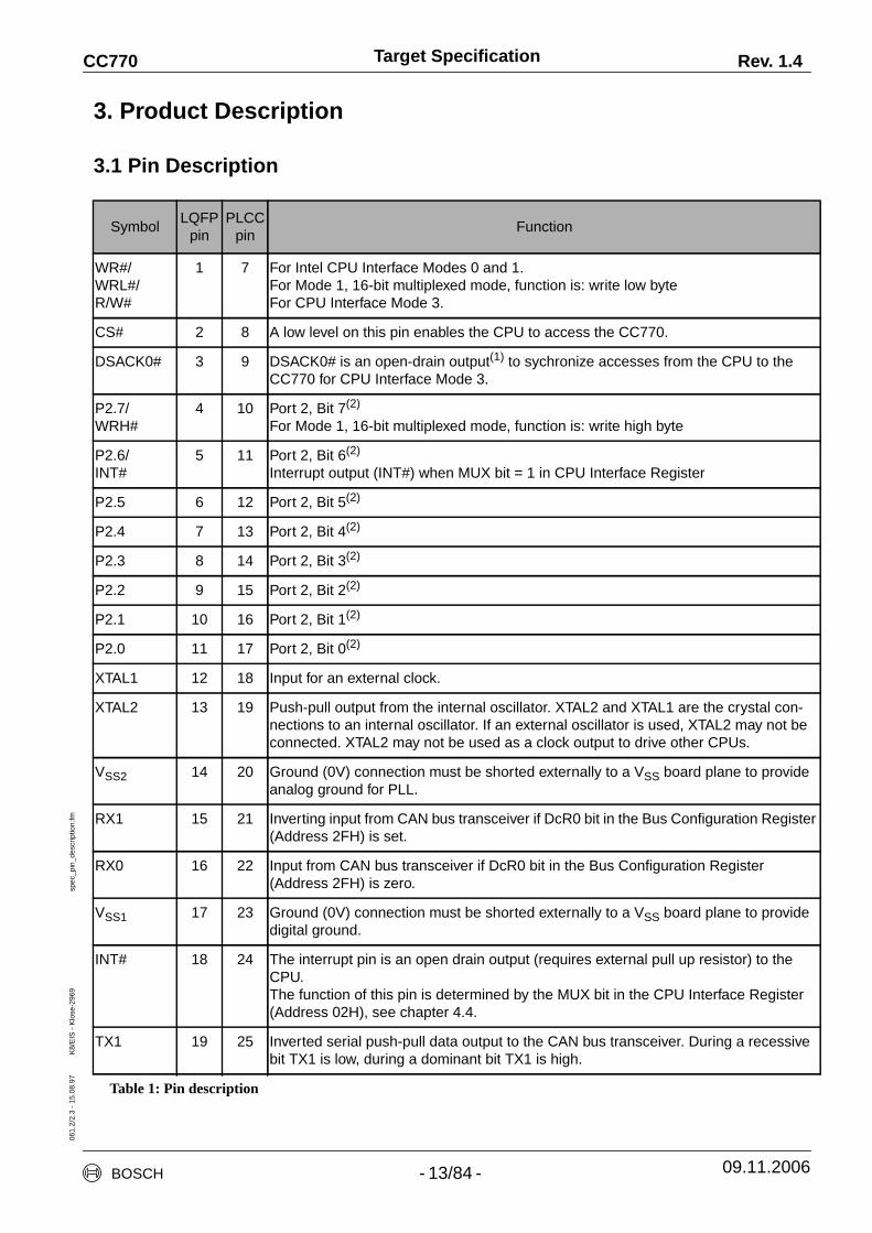
3. Product Description
3.1 Pin Description
SymbolLQFP
pinPLCC
pinFunction
WR#/WRL#/R/W#
1 7 For Intel CPU Interface Modes 0 and 1.For Mode 1, 16-bit multiplexed mode, function is: write low byteFor CPU Interface Mode 3.
CS# 2 8 A low level on this pin enables the CPU to access the CC770.
DSACK0# 3 9 DSACK0# is an open-drain output(1) to sychronize accesses from the CPU to theCC770 for CPU Interface Mode 3.
P2.7/WRH#
4 10 Port 2, Bit 7(2)
For Mode 1, 16-bit multiplexed mode, function is: write high byte
P2.6/INT#
5 11 Port 2, Bit 6(2)
Interrupt output (INT#) when MUX bit = 1 in CPU Interface Register
P2.5 6 12 Port 2, Bit 5(2)
P2.4 7 13 Port 2, Bit 4(2)
P2.3 8 14 Port 2, Bit 3(2)
P2.2 9 15 Port 2, Bit 2(2)
P2.1 10 16 Port 2, Bit 1(2)
P2.0 11 17 Port 2, Bit 0(2)
XTAL1 12 18 Input for an external clock.
XTAL2 13 19 Push-pull output from the internal oscillator. XTAL2 and XTAL1 are the crystal con-nections to an internal oscillator. If an external oscillator is used, XTAL2 may not beconnected. XTAL2 may not be used as a clock output to drive other CPUs.
VSS2 14 20 Ground (0V) connection must be shorted externally to a VSS board plane to provideanalog ground for PLL.
RX1 15 21 Inverting input from CAN bus transceiver if DcR0 bit in the Bus Configuration Register(Address 2FH) is set.
RX0 16 22 Input from CAN bus transceiver if DcR0 bit in the Bus Configuration Register(Address 2FH) is zero.
VSS1 17 23 Ground (0V) connection must be shorted externally to a VSS board plane to providedigital ground.
INT# 18 24 The interrupt pin is an open drain output (requires external pull up resistor) to theCPU.The function of this pin is determined by the MUX bit in the CPU Interface Register(Address 02H), see chapter 4.4.
TX1 19 25 Inverted serial push-pull data output to the CAN bus transceiver. During a recessivebit TX1 is low, during a dominant bit TX1 is high.
Table 1: Pin description
BOSCH - 13/84 - 09.11.2006spec_pin_description.fm

Target Specification Rev. 1.4CC77006
1.2/
2.3
- 15
.08.
97
K8/
EIS
- K
lose
-296
9sp
ec_p
in_d
escr
iptio
n.fm
TX0 20 26 Serial push-pull data output to the CAN bus transceiver. During a recessive bit TX0 ishigh, during a dominant bit TX0 is low.
CLKOUT 21 27 Programmable clock output. This push-pull output may be used to drive the clockinput of the CPU.
READY/
MISO
22 28 READY is an open-drain output to synchronize accesses from the CPU to the CC770for CPU Interface Modes 0 and 1.MISO is the serial push-pull data output in the SPI mode.
RESET# 23 29 Warm Reset: (VCC remains valid while RESET# is asserted), RESET# must bedriven to a low level for 1 µs minimum.Cold Reset: (VCC is driven to a valid level while RESET# is asserted)RESET# must be driven low for 1 ms minimum (measured from a valid VCC level) toensure the oscillator and the PLL is stabile. No falling edge on the Reset pin isrequired during a cold reset event.
Mode1 24 30 Select, together with Pin 44, one of the four parallel interface modes.(3)
P1.7-0 25-32 31-38 Port 1 with multi Function Pins, see Table 2.(2)
AD7-3 33-37 39-43 Multi Function Pins, see Table 2.
Mode0 38 44 Select, together with Pin 30, one of the four parallel interface modes. See chapter7.1.(3)
VCC 39 1 Power connection must be shorted externally to +5V DC to provide power to theentire chip.
AD2-0 40-42 2 - 4 Multi Function Pin, see Table 2.
ALE/AS
43 5 ALE used for CPU Interface Modes 0 and 1.AS used for Motorola modes. (In Mode 3, pin must be tied high.)
RD#/E
44 6 RD# used for CPU Interface Modes 0 and 1.E used for Motorola modes. (In Mode 3 Asynchronous, pin must be tied high.)
SymbolLQFP
pinPLCC
pinFunction
Table 1: Pin description
BOSCH - 14/84 - 09.11.2006

Target Specification Rev. 1.4CC77006
1.2/
2.3
- 15
.08.
97
K8/
EIS
- K
lose
-296
9sp
ec_p
in_d
escr
iptio
n.fm
Notes to pin descriptions:(1) DSACK0# is often used as a pulldown output with a 3.3 kΩ pullup resistor and a 100 pFload capacitance. An open-drain output is used because several peripherals may be con-nected to the DSACK0# line. The CC770 specifies a TCHKH timing (CS# high to DSACK0#high) equal to 55 ns, however a 3.3 kΩ resistor will not sufficiently charge the line whenDSACK0# is floated by the CC770. To meet this timing, the CC770 has an active pullup thatdrives the DSACK0# output until it is high, and then the pullup is turned off. Therefore, thepullup is active for a short time only.
(2) Port1 and Port2 pins are weakly held high until the Port Configuration Registers havebeen written (locations 9FH and AFH respectively).
(3) Mode0 and Mode1 pins are internally connected to weak pulldowns. These pins will bepulled low during reset if unconnected. Following reset, these pins float.
SymbolLQFP
pinPLCC
pin
Mode 08-BitIntel
Multiplexed
Mode 116-BitIntel
Multiplexed
Mode 28-Bit
MotorolaMultiplexed
Mode 38-BitNon-
Multiplexed
SPI-Mode
SerialInterface
AD0 42 4 AD0 AD0 AD0 A0 ICP
AD1 41 3 AD1 AD1 AD1 A1 CP
AD2 40 2 AD2 AD2 AD2 A2 CSAS
AD3 37 43 AD3 AD3 AD3 A3 STE
AD4/MOSI 36 42 AD4 AD4 AD4 A4 MOSI
AD5 35 41 AD5 AD5 AD5 A5 Unused
AD6/SCLK 34 40 AD6 AD6 AD6 A6 SCLK
AD7 33 39 AD7 AD7 AD7 A7 Unused
P1.0/AD8 32 38 P1.0 AD8 P1.0 D0 P1.0
P1.1/AD9 31 37 P1.1 AD9 P1.1 D1 P1.1
P1.2/AD10 30 36 P1.2 AD10 P1.2 D2 P1.2
P1.3/AD11 29 35 P1.3 AD11 P1.3 D3 P1.3
P1.4/AD12 28 34 P1.4 AD12 P1.4 D4 P1.4
P1.5/AD13 27 33 P1.5 AD13 P1.5 D5 P1.5
P1.6/AD14 26 32 P1.6 AD14 P1.6 D6 P1.6
P1.7/AD15 25 31 P1.7 AD15 P1.7 D7 P1.7
Table 2: Multi Function Pins
BOSCH - 15/84 - 09.11.2006
Target Specification Rev. 1.4CC77006
1.2/
2.3
- 15
.08.
97
K8/
EIS
- K
lose
-296
9sp
ec_p
in_d
escr
iptio
n.fm
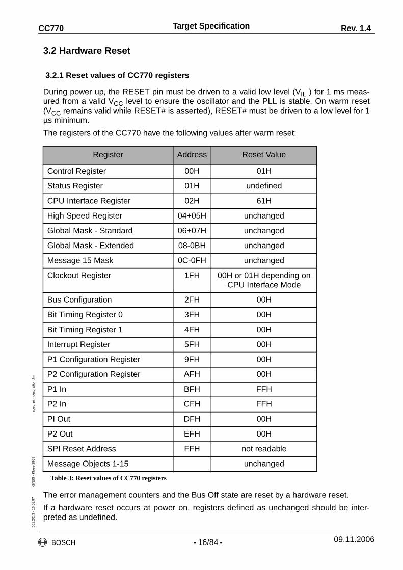
3.2 Hardware Reset
3.2.1 Reset values of CC770 registers
During power up, the RESET pin must be driven to a valid low level (VIL ) for 1 ms meas-ured from a valid VCC level to ensure the oscillator and the PLL is stable. On warm reset(VCC remains valid while RESET# is asserted), RESET# must be driven to a low level for 1µs minimum.
The registers of the CC770 have the following values after warm reset:
The error management counters and the Bus Off state are reset by a hardware reset.
If a hardware reset occurs at power on, registers defined as unchanged should be inter-preted as undefined.
Register Address Reset Value
Control Register 00H 01H
Status Register 01H undefined
CPU Interface Register 02H 61H
High Speed Register 04+05H unchanged
Global Mask - Standard 06+07H unchanged
Global Mask - Extended 08-0BH unchanged
Message 15 Mask 0C-0FH unchanged
Clockout Register 1FH 00H or 01H depending onCPU Interface Mode
Bus Configuration 2FH 00H
Bit Timing Register 0 3FH 00H
Bit Timing Register 1 4FH 00H
Interrupt Register 5FH 00H
P1 Configuration Register 9FH 00H
P2 Configuration Register AFH 00H
P1 In BFH FFH
P2 In CFH FFH
PI Out DFH 00H
P2 Out EFH 00H
SPI Reset Address FFH not readable
Message Objects 1-15 unchanged
Table 3: Reset values of CC770 registers
BOSCH - 16/84 - 09.11.2006

Target Specification Rev. 1.4CC77006
1.2/
2.3
- 15
.08.
97
K8/
EIS
- K
lose
-296
9sp
ec_p
in_d
escr
iptio
n.fm
3.2.2 Reset values of CC770 output pins
The behaviour of CC770 output pins in reset procedure:
3.3 Software Initialization
Software initialization is started by setting the Init bit in the Control Register, either by soft-ware, hardware reset, or by going Bus Off. While Init is set, all message transfers to andfrom the CC770 are stopped and the TX0 and TX1 outputs are recessive. The errorcounters are unchanged. Initialization is used to configure the CC770 memory withoutinterference to or by CAN bus.
Resetting Init bit completes initialization and the CC770 synchronizes itself to the CAN busby waiting for 11 consecutive recessive bits (called bus idle) before it will take part in busactivities.
Note:
The Bus Off recovery sequence (see CAN Specification Rev. 2.0) cannot be shortened bysetting or resetting Init. If the device goes Bus Off, it will set Init of its own accord, stoppingall bus activities. Once Init has been cleared by the CPU, the device will then wait for 129occurrences of Bus Idle (129 * 11 consecutive recessive bits) before resuming normal oper-ations. At the end of the Bus Off recovery sequence, the Error Management Counters willbe reset.
During the waiting time after the resetting of Init, each time a sequence of 11 recessive bitshas been monitored, a Bit0Error code is written to the Status Register, enabling the CPU toreadily check up whether the CAN bus is stuck at dominant or continuously disturbed and tomonitor the proceeding of the Bus Off recovery sequence.
Software initialization does not change configuration register values.
3.4 Configuration of Bit Timing
After setting bits Init and CCE in the CAN Control Register, the bit timing can be configuredby writing to the Bit Timing Registers.
Pinoutput state
while reset is activeoutput state
direct after reset
Mode 0/1 weakly pulled low high impedance
Port 1/2 weakly pulled high high impedance input
Clockout active
TX0 1 (recessive)
TX1 0 (recessive)
INT# float
DSACK0# float
Table 4: Reset states of CC770 output pins
BOSCH - 17/84 - 09.11.2006

Target Specification Rev. 1.4CC77006
1.2/
2.3
- 15
.08.
97
K8/
EIS
- K
lose
-296
9sp
ec_p
in_d
escr
iptio
n.fm
While Bit Timing Register 0 controls the (Re)Synchronisation Jump Width and the BaudRate Prescaler, Bit Timing Register 1 is used to define the position of the Sample Pointinside a Bit Time. For a detailed description how to program the bit timing see chapter 4.14.
3.5 Silent Mode
The CAN Controller can be set in Silent Mode by programming the Bus Configuration Reg-ister bits DcR1 and DcR0 both to one.
In Silent Mode, the CC770 is able to receive valid data frames and valid remote frames, butit sends only recessive bits on the CAN bus and it cannot start a transmission. If the CANController is required to send a dominant bit (ACK bit, overload flag, active error flag), thebit is rerouted internally so that the CAN Controller monitors this dominant bit, although theCAN bus may remain in recessive state.
The Silent Mode can be used to analyze the traffic on a CAN bus without affecting it by thetransmission of dominant bits (Acknowledge Bits, Error Frames).
3.6 Low Current Modes
Power Down and Sleep Modes are activated by the PwD and Sleep bits in the CPU Inter-face Register (02H) under the control of the programmer.
During Power Down and Sleep Mode the CPU Interface Register is the only accessible reg-ister. In this mode the oscillator is not active and no access to the message objects is possi-ble.
The CC770 exits from Power Down by either a hardware reset or by resetting the PwD bit to"0". The CPU must read the hardware reset bit (bit 7, register 02H) to ensure the CC770has exited Power Down.
The CC770 enters Sleep Mode after the Sleep bit in the CPU Interface Register (bit 3, reg-ister 02H) is set and a possibly ongoing transmission on the CAN Bus has finished.
Sleep mode is exited by resetting the Sleep bit or when there is activity on the CAN bus.The CC770 requires a minimum of 10 ms to come out of Sleep Mode after bus activityoccurs to ensure the oscillator and the PLL is stabile.
Power Down and Sleep Mode should not be entered directly after reset. The user programmust perform a minimum Memory configuration at any time (preferably during the initializa-tion) prior to entering these modes.
Programming the following registers satisfies the minimum configuration requirement:
• Control Register (00H) (set CCE bit to "1")
• CPU Interface Register (02H) (DMC bit application specific)
• Bit Timing Register 0 (3FH) (application specific)
• Bit Timing Register 1 (4FH) (application specific)
• All MO Control 0 Registers (reset MsgVal bit to "0")
• Control Register (00H) (reset Init and CCE bits to "0")
BOSCH - 18/84 - 09.11.2006
Target Specification Rev. 1.4CC77006
1.2/
2.3
- 15
.08.
97
K8/
EIS
- K
lose
-296
9sp
ec_f
unct
iona
l_de
scrip
tion.
fm
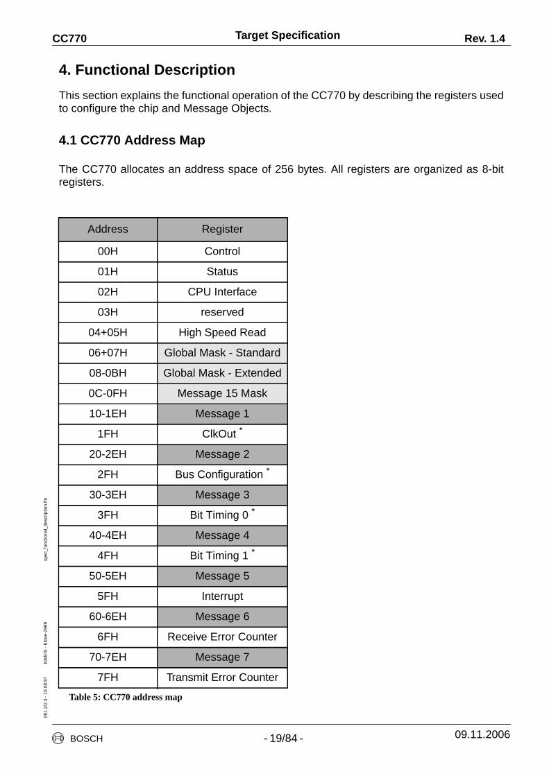
4. Functional Description
This section explains the functional operation of the CC770 by describing the registers usedto configure the chip and Message Objects.
4.1 CC770 Address Map
The CC770 allocates an address space of 256 bytes. All registers are organized as 8-bitregisters.
Address Register
00H Control
01H Status
02H CPU Interface
03H reserved
04+05H High Speed Read
06+07H Global Mask - Standard
08-0BH Global Mask - Extended
0C-0FH Message 15 Mask
10-1EH Message 1
1FH ClkOut *
20-2EH Message 2
2FH Bus Configuration *
30-3EH Message 3
3FH Bit Timing 0 *
40-4EH Message 4
4FH Bit Timing 1 *
50-5EH Message 5
5FH Interrupt
60-6EH Message 6
6FH Receive Error Counter
70-7EH Message 7
7FH Transmit Error Counter
Table 5: CC770 address map
BOSCH - 19/84 - 09.11.2006spec_functional_description.fm
Target Specification Rev. 1.4CC77006
1.2/
2.3
- 15
.08.
97
K8/
EIS
- K
lose
-296
9sp
ec_f
unct
iona
l_de
scrip
tion.
fm
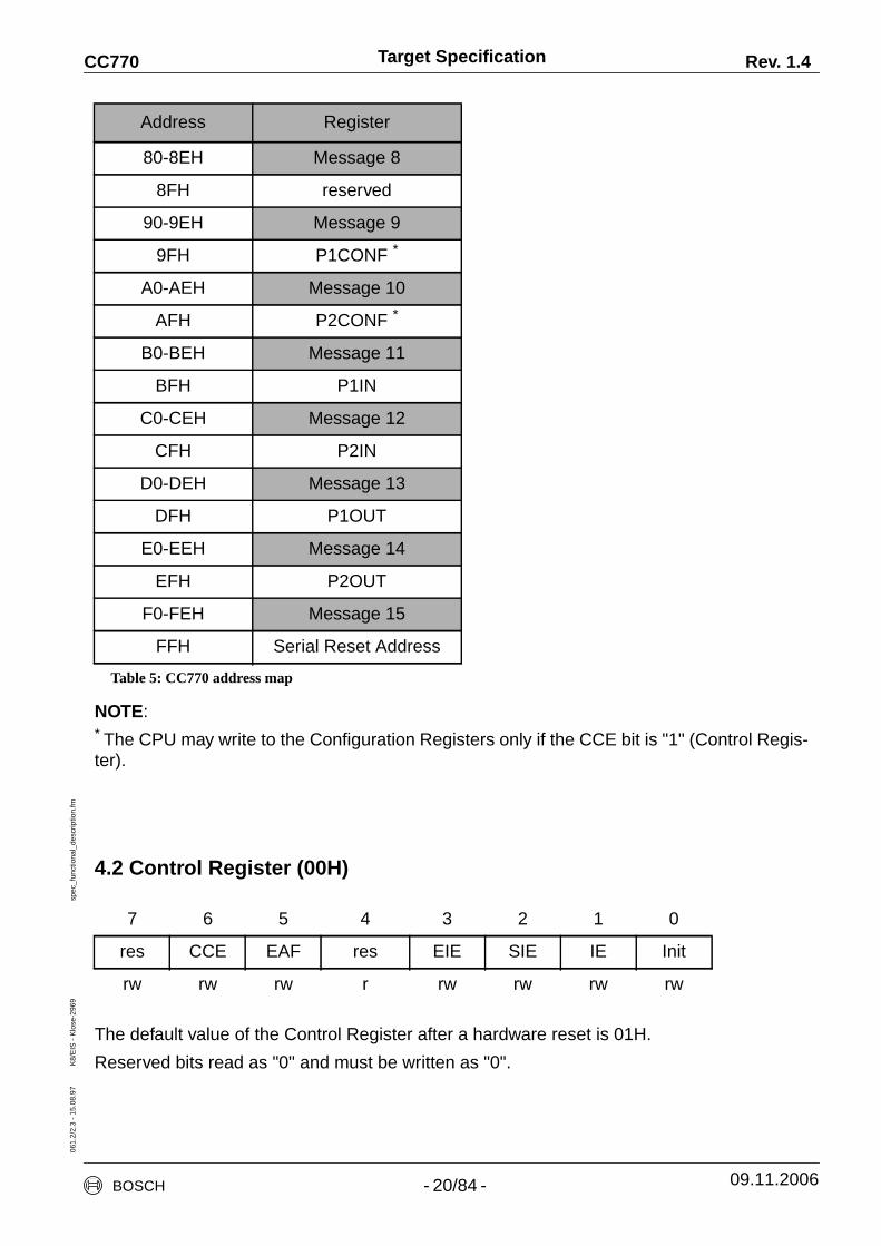
NOTE:* The CPU may write to the Configuration Registers only if the CCE bit is "1" (Control Regis-ter).
4.2 Control Register (00H)
The default value of the Control Register after a hardware reset is 01H.
Reserved bits read as "0" and must be written as "0".
80-8EH Message 8
8FH reserved
90-9EH Message 9
9FH P1CONF *
A0-AEH Message 10
AFH P2CONF *
B0-BEH Message 11
BFH P1IN
C0-CEH Message 12
CFH P2IN
D0-DEH Message 13
DFH P1OUT
E0-EEH Message 14
EFH P2OUT
F0-FEH Message 15
FFH Serial Reset Address
7 6 5 4 3 2 1 0
res CCE EAF res EIE SIE IE Init
rw rw rw r rw rw rw rw
Address Register
Table 5: CC770 address map
BOSCH - 20/84 - 09.11.2006

Target Specification Rev. 1.4CC77006
1.2/
2.3
- 15
.08.
97
K8/
EIS
- K
lose
-296
9sp
ec_f
unct
iona
l_de
scrip
tion.
fm
CCE Change Configuration Enable
one The CPU has write access to the Configuration Registers (ClkOut, Bus Config-uration,...). Init bit should be set in order to stop CAN bus activities, if the valuesin the Bit Timing Registers must be changed.
zero The CPU has no write access to the Configuration Registers.
This bit is reset by the CPU to provide protection against unintentional rewriting of criticalregisters by the CPU following the initialization sequence.
EAF Enable Additional Functions
one The Receive Error Counter (address 6FH) and the Transmit Error Counter(address 7FH) can be read. The additional mask bits MDir and MXtd in theMessage 15 Mask are enabled.
zero The addresses 6FH and 7FH are reserved. The additional mask bits MDir andMXtd in the Message 15 Mask are disabled and will be read as 00, independentof the last value written to those bits while EAF was "1".
The CC770 provides additional functions giving the programmer the possibility to read theError Counters and to mask Xtd and Dir bits in the Message 15 Mask, allowing the recep-tion of all possible messages not received by other Message Objects.
To enable this functions the programmer has to set the EAF bit. In the AN82527 this bit isreserved and must not be set to 1.
EIE Error Interrupt Enable
one Error interrupts enabled. A change in the error status of the CC770 will causean interrupt to be generated.
zero Error interrupts disabled. No error interrupt will be generated.
Error interrupts are BOff and Warn in the Status Register. Error Interrupt Enable is set bythe CPU to allow the CC770 to interrupt CPU when an abnormal number of CAN bus errorshave been detected.
It is recommended to enable this interrupt during normal operation.
SIE Status Change Interrupt Enable
one Status Change Interrupt enabled. An interrupt will be generated when a CANbus error is detected in the Status Register or a transfer (reception or transmis-sion) is successfully completed, independent of the interrupt enable bits in anyMessage Object.
zero Status Change Interrupt disabled. No status interrupt will be generated.
Status Change Interrupts are WakeUp, RxOK, TxOK, and LEC0-2 in the Status Register.
RxOK occurs upon every successful message transmission on the CAN bus, regardless ofwhether the message is stored by the CC770.
The LEC bits are very helpful to indicate whether Bit or Form Errors are occurring. In nor-mal operation it is not advised to enable this interrupt for LEC since the CAN protocol wasdesigned to handle these error conditions in hardware by error frames and the automatic
BOSCH - 21/84 - 09.11.2006
Target Specification Rev. 1.4CC77006
1.2/
2.3
- 15
.08.
97
K8/
EIS
- K
lose
-296
9sp
ec_f
unct
iona
l_de
scrip
tion.
fm
retransmission of messages. When cumulative LEC occur, the warning and BusOff flagswill be set. The Error Interrupt should be enabled to detect these conditions.
In most applications, the SIE bit should not be set. Since this interrupt will occur for everymessage, the CPU will be unnecessarily burdened. Instead, interrupts should be imple-mented on a Message Object basis so interrupts occur only for messages that are used bythe CPU.
The SIE bit is set by the CPU.
NOTE:
If the Status Change Interrupts and Message Object receive/transmit interrupts are ena-bled, there will be two interrupts for each message successfully received or transmitted by aMessage Object.
IE Interrupt Output Enable
one Interrupt Pin enabled.
zero Interrupt Pin disabled. The CC770 will generate no interrupts although theInterrupt Register (5FH) will still be updated.
Applies to EIE, SIE, and Message Object Tx/Rx interrupts. For example the Interrupt Regis-ter (5FH) contains a value other than zero, indicating the interrupt source (Message Objector Status), and the IE bit is set to one, an interrupt will be generated. No interrupt will be lostbecause of periodic setting or resetting of this bit.
The Interrupt Output Enable bit is set by the CPU.
INIT Initialization
one Software initialization is enabled.
zero Software initialization is disabled.
Following a hardware reset, this bit will be set.
The Init bit is written by the CPU and is set by the CC770 when it goes busoff. Initializationis a state which allows the user to configure the CC770 Memory without the chip participat-ing in any CAN bus transmissions. While Init equals one, all message transfers to and fromthe CAN bus are stopped, and the status of the CAN bus output Tx is recessive. Initializa-tion will most often be used the first time after power-up and when the CC770 has removeditself from the CAN bus after going busoff.
Init should not be used in normal operation when the CPU is modifying transmit data; theCPUUpd bit in the Control 1 register from each Message Object is used in this case.
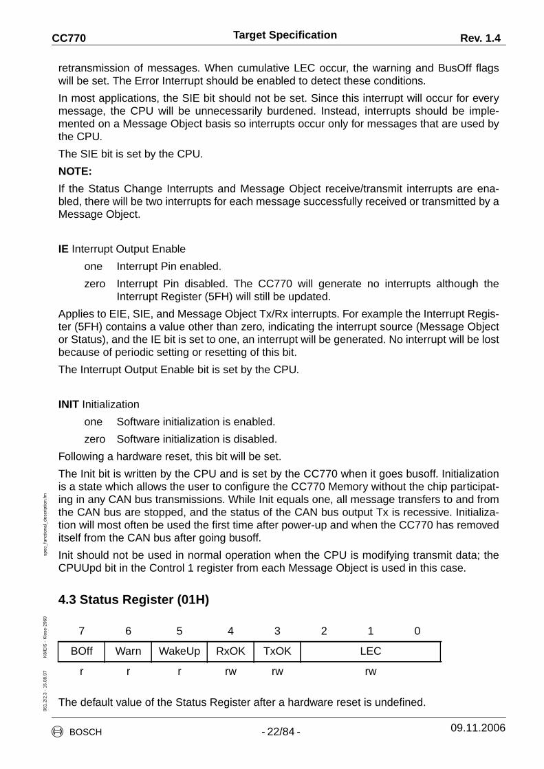
4.3 Status Register (01H)
The default value of the Status Register after a hardware reset is undefined.
7 6 5 4 3 2 1 0
BOff Warn WakeUp RxOK TxOK LEC
r r r rw rw rw
BOSCH - 22/84 - 09.11.2006

Target Specification Rev. 1.4CC77006
1.2/
2.3
- 15
.08.
97
K8/
EIS
- K
lose
-296
9sp
ec_f
unct
iona
l_de
scrip
tion.
fm
BOff Bus Off Status
one There is an abnormal rate of occurrences of errors on the CAN bus.
zero The CC770 is not busoff.
The Bus Off condition occurs when the Transmit Error Counter in the CC770 has reachedthe limit of 256. In consequence, the CC770 going busoff. During busoff, no messages canbe received or transmitted.
The only way to exit this state is by resetting the Init bit in the Control Register (location00H). When this bit is reset, the busoff recovery sequence begins. The busoff recoverysequence resets the Transmit and Receive Error Counters. After the CC770 counts 128packets of 11 consecutive recessive bits on the CAN bus, the busoff state is exited.
The Bus Off Status bit is written by the CC770.
Warn Warning Status
one There is an abnormal rate of occurrences of errors on the CAN bus.
zero There is no abnormal occurrence of errors.
The Warning condition occurs when an error counter in the CC770 has reached the limit of96. When this bit is set, an interrupt will occur if the EIE and IE bits of the Control Register(00H) are set.
The Warning Status bit is written by the CC770.
WakeUp Wake Up Status
one The CC770 has left Power Down or Sleep mode.
zero No wake up.
Setting the Sleep bit in CPU Interface register (02H) to "1" will place the CC770 into Sleepmode. While in Sleep mode, the WakeUp bit is "0". The WakeUp bit will become "1" whenbus activity is detected or when the CPU writes the Sleep bit to "0". The WakeUp bit willalso be set to "1" after the CC770 comes out of Power Down mode.
The WakeUp bit and WakeUp interrupt is reset by reading the Status Register.
This bit is written by the CC770.
RxOK Receive Message Successfully
one Since this bit was last reset to zero by the CPU, a message has been success-fully received.
zero Since this bit was last reset by the CPU, no message has been successfullyreceived.
This bit is never reset by the CC770. A successfully received message may be any CANbus transmission that is error-free, regardless of whether the CC770 has configured a Mes-sage Object to receive that particular message identifier.
The CC770 will set this bit, the CPU may clear it.
BOSCH - 23/84 - 09.11.2006
Target Specification Rev. 1.4CC77006
1.2/
2.3
- 15
.08.
97
K8/
EIS
- K
lose
-296
9sp
ec_f
unct
iona
l_de
scrip
tion.
fm
TxOK Transmit Message Successfully
one Since this bit was last reset to zero by the CPU, a message has been success-fully transmitted (error free and acknowledged by at least one other node).
zero Since this bit was last reset by the CPU, no message has been successfullytransmitted.
This bit is never reset by the CC770.
The CC770 will set this bit, the CPU may clear it.
LEC Last Error Code
0 No error
1 Stuff Error
More than 5 equal bits in a sequence have occurred in a part of a receivedmessage where this is not allowed.
2 Form Error
The fixed format part of a received frame has the wrong format.
3 Acknowledgment Error (AckError)
The message transmitted by this device was not acknowledged by anothernode.
4 Bit 1 Error
During the transmission of a message (with the exception of the arbitrationfield), the CC770 wanted to send a recessive level (bit of logical value 1), butthe monitored CAN bus value was dominant.
5 Bit 0 Error
During the transmission of a message, the CC770 wanted to send a dominantlevel (bit of logical value 0), but the monitored CAN bus value was recessive.During busoff recovery, this status is set each time a recessive bit is received(indicating the CAN bus is not stuck dominant).
6 CRC Error
The CRC checksum was incorrect in the message received. The CRC receivedfor an incoming message does not match with the CRC value calculated by thisdevice for the received data.
7 Unused
This field contains a code which indicates the type of the first error to occur in a frame onthe CAN bus. If a message has been transferred (reception or transmission) without error,this field will be cleared to ‘0’.
The code ‘7’ is unused and may be written by the CPU to check for updates.
4.3.1 Status Interrupts
If the SIE bit in the Control Register (00H) is set and the CC770 has updated the StatusRegister, the Interrupt Register (5FH) will contain a "1". The Status Register must be read if
BOSCH - 24/84 - 09.11.2006

Target Specification Rev. 1.4CC77006
1.2/
2.3
- 15
.08.
97
K8/
EIS
- K
lose
-296
9sp
ec_f
unct
iona
l_de
scrip
tion.
fm
a Status Change Interrupt occurs. Reading the Status Register will clear the Status ChangeInterrupt.
A Status Change Interrupt will occur on every successful reception or transmission, regard-less of the state of the RxOK and TxOK bits. Therefore, if TxOK is set and a subsequenttransmission occurs, an interrupt will occur (if enabled) even though TxOK was previouslyequal to one.
There are two ways to implement receive and transmit interrupts. The difference betweenthese two methods is one relies on the hardwired priority of the Message Objects and theother is suitable for polling.
The first and preferred method uses the TxIE and RxIE bits in the Control 0 register for eachcorresponding Message Object. Whenever a message is transmitted or received by thisMessage Object, the corresponding interrupt is serviced in accordance with its priority (ifthe IE bit of register 00H is set). This method uses the hardwired priority scheme of theCC770 which requires minimal CPU intervention.
The second method sets the SIE bit of the Control Register (00H) to "1" which will force aninterrupt whenever successful message transmissions or receptions occur. The TxOK bitwill be set when any of the Message Objects transmits a message. The RxOK bit will be seton any successfully received message. This may be any CAN bus transmission that iserror-free, regardless of whether the CC770 has configured a Message Object to receivethat particular message identifier. This method allows the user to more easily define theinterrupt priority of each Message Object by polling the Message Objects following an SIEinterrupt.
4.4 CPU Interface Register (02H)
The value of the CPU Interface Register during the hardware reset is E1H, after the end ofthe hardware reset the default value is 41H.
RstSt Hardware Reset Status
one The hardware reset of the CC770 is active (RESET is low). While reset isactive, no access to the CC770 is possible, except read access on the CPUinterface register.
zero Normal operation.
The CPU must ensure this bit is zero before further access to the CC770 after reset.
This bit is written by the CC770.
DSC Divide System Clock (SCLK).
one The system clock is equal to XTAL/2.
zero The system clock is equal to XTAL.
This bit is written by the CPU.
7 6 5 4 3 2 1 0
RstST DSC DMC PwD Sleep MUX StEn CEn
r rw rw rw rw rw rw rw
BOSCH - 25/84 - 09.11.2006
Target Specification Rev. 1.4CC77006
1.2/
2.3
- 15
.08.
97
K8/
EIS
- K
lose
-296
9sp
ec_f
unct
iona
l_de
scrip
tion.
fm
DMC Divide Memory Clock (MCLK)
one The memory clock is equal to SCLK/2.
zero The memory clock is equal to SCLK.
This bit is written by the CPU.
PwD Power Down Mode enable and Sleep Mode enable
Information about low Current Modes see chapter 3.6.
The Sleep bit and the Power Down bit may be set and reset by the CPU. The Sleep bit willalso be reset by CAN bus activity during Sleep Mode.
MUX (see text below)
one Pin 24 = float, pin 11 = INT#.
zero Normal operation: Pin 24 = INT#, Pin 11 = P2.6.
This bit is written by the CPU.
Bit 2 (MUX) controls whether the interrupt output is available at pin 11 (MUX = 1) or pin 24(MUX = 0). The AN82527 provides an output voltage of VCC/2 at pin 24 if MUX = 1 to sup-port an "ISO low speed physical layer". The CC770 lets pin 24 float if MUX = 1, assumingan appropriate CAN bus driver IC is utilized.
StEn Clockout Stretch Enable
one The Clockout for the CPU is stretched to lengthen the read and write cycles ofthe CC770 instead of generating wait states.Example: CPU read data from CC770When the CPU writes the address byte to the CC770 the Clockout is disabled,until the data of the selected address is available for read.
zero The Clockout is not streched.
CEn Clockout enable
one Clockout signal is enabled, (default after reset).
zero Clockout signal is disabled.
PwD Sleep Function
0 0 Both Power Down and Sleep Modes are not active.
0 1 Sleep Mode is active. These bits are written by the CPU.
1 X Power Down Mode is active.
Table 6: Function of Power Down and Sleep bits
BOSCH - 26/84 - 09.11.2006
Target Specification Rev. 1.4CC77006
1.2/
2.3
- 15
.08.
97
K8/
EIS
- K
lose
-296
9sp
ec_f
unct
iona
l_de
scrip
tion.
fm
Accesses to the CPU Interface Register are asynchronous, so it is possible to read andwrite this register even if there is no clock input or during Power Down Mode and SleepMode.
4.4.1 Clocking Description
There are two analogue clocks and four digital clocks in the CC770. The analogue clocksare the crystal oscillator clock (XTAL) and the PLL clock (PLLCLK). The digital clocks arethe system clock (SCLK), the memory clock (MCLK), the Clockout pin signal, and the SPIclock (SPICLK). While the SPI clock is directly controlled by the SPI master, the other digitalclocks are derived from the analogue clocks.
The PLLCLK (two times the frequency of XTAL) is provided as clock source for SCLK inorder to allow a sufficient system clock frequency SCLK for high CAN bit rates at a moder-ate XTAL frequency. The balanced two-phase clock SCLK is always the result of a divide-by-2; CPU Interface Register's bit DSC decides whether the PLL (DSC="0", SCLK=XTAL)or XTAL (DSC=”1”, SCLK=XTAL/2) is the source of SCLK. SCLK is the clock of the CAN'sbit timing and other CAN protocol functions.
The memory clock MCLK is derived from SCLK, it is either the same as SCLK (DMC=”0”) orit is SCLK/2 (DMC=”1”), compensating for the limited clocking range of the CC770's Con-tent Addressable Memory (CAM).
The Clockout pin signal is always derived from PLLCLK, its actual frequency is controlledby the CDv value in the ClkOut register (1FH).
If the Clockout pin is not used and the SCLK frequency is sufficient at XTAL/2, then the PLLshould be disabled in order to reduce the CC770's electromagnetic interference (EMI). Thisis done by setting DSC="1", StEn="1", and CEn="0".
When the PLL is enabled, the minimum XTAL frequency is 8 MHz. Since the CC770'sdesign is fully static, the XTAL frequency may be lower than 8 MHz when the crystal at theXTAL pins is replaced by a clock generator and the PLL is disabled.
Notes:
Frequency of SCLK = fXTAL/(1 + DSC bit)
Frequency of MCLK = fSCLK/(1 + DMC bit) = fXTAL/[(1 + DSC bit) * (1 + DMC bit)]
fXTAL SCLK MCLK DSC bit DMC bit
8 MHz 8 MHz 8 MHz 0 0
10 MHz 10 MHz 5 MHz 0 1
12 MHz 6 MHz 6 MHz 1 0
16 MHz 8 MHz 8 MHz 1 0
20 MHz 10 MHz 5 MHz 1 1
Table 7: Maximum MCLK frequency for various oscillator frequencies
BOSCH - 27/84 - 09.11.2006

Target Specification Rev. 1.4CC77006
1.2/
2.3
- 15
.08.
97
K8/
EIS
- K
lose
-296
9sp
ec_f
unct
iona
l_de
scrip
tion.
fm
4.5 High Speed Read Register (04+05H)
High Speed Read Register (04H)
High Speed Read Register (05H)
The value of the High Speed Read register is not affected by a hardware reset.
The High Speed Read register is a read only register and is the output buffer for the CPUInterface Logic. This register is part of the CPU Interface Logic and is not located in theRAM.
During a read to the RAM (low speed registers) this register is loaded with the value of thelow speed register being accessed.
The High Speed Read register is available to provide a method to read the CC770 when theCPU (host microcontroller) is unable to satisfy read cycle timings for low speed CC770 reg-isters. In other words, if the read access time of the CC770 is too slow for the CPU and theCPU cannot extend the read bus cycle, the following double read method should be used.
4.5.1 Double Read Operation
The CPU can execute double reads where the first read addresses the low speed registerand the second read addresses the High Speed Read register. The first read is a dummyread for the CPU, however the low speed register value is stored in the High Speed Readregister. The second read to the High Speed Read register will provide the data from thedesired low speed register.
The advantage of double reads is both read operations have fast access times. The firstread of the low speed register requires 40 ns (verify in current data sheet) to load the HighSpeed Read Register (the data on the address/data pins is not valid). The second read ofthe High Speed Read register requires 45 ns (verify in current data sheet) and the data onthe address/data bus is valid.
Therefore, if the access time of a low speed register is too long for the CPU then a secondread to the High Speed Register will produce the correct data. Please note Low and HighSpeed registers have different access timing specifications in the CC770 data sheet.
During a 16-bit read access the low and high byte will contain the 16-bit value from the readaccess. For an 8-bit read access the low byte will contain the value from the read access.
7 6 5 4 3 2 1 0
Low Byte
r
7 6 5 4 3 2 1 0
High Byte
r
BOSCH - 28/84 - 09.11.2006

Target Specification Rev. 1.4CC77006
1.2/
2.3
- 15
.08.
97
K8/
EIS
- K
lose
-296
9sp
ec_f
unct
iona
l_de
scrip
tion.
fm
4.6 Global Mask - Standard Register (06-07H)
Global Mask (06H)
Global Mask (07H)
The value of the Global Mask Standard is not affected by a hardware reset.
Reserved bits read as "1".
Mskx Mask bit at position X
one must-match (incoming bit value must match to the corresponding bit in the Arbi-tration Register from a Message Object)
zero don’t care (accept a "0" or "1" for that bit position)
The Global Mask Standard register applies only to messages using the standard CAN Iden-tifier and thereby to Message Objects with the Xtd bit set to "0". This feature, also calledmessage acceptance filtering, allows the user to Globally Mask, or “don’t care” any identi-fier bits of the incoming message. This mask is programmable to allow the user to developan application specific masking strategy.
Note:
When a remote frame is sent, an CC770 receiver node will use the Global Mask Registersto determine whether the remote frame matches to any of its Message Objects. If theCC770 is programmed to transmit a message in response to a remote frame messageidentifier, the CC770 will transmit a message with the message identifier of the CC770 Mes-sage Object. The result is the remote message and the responding CC770 transmit mes-sage may have different message identifiers because some CC770 Global Mask Registerbits are "don’t care".
4.7 Global Mask - Extended Register (08-0BH)
Global Mask Extended (08H)
7 6 5 4 3 2 1 0
Msk28 Msk27 Msk26 Msk25 Msk24 Msk23 Msk22 Msk21
rw rw rw rw rw rw rw rw
7 6 5 4 3 2 1 0
Msk20 Msk19 Msk18 res
rw rw rw r
7 6 5 4 3 2 1 0
Msk28 Msk27 Msk26 Msk25 Msk24 Msk23 Msk22 Msk21
rw rw rw rw rw rw rw rw
BOSCH - 29/84 - 09.11.2006

Target Specification Rev. 1.4CC77006
1.2/
2.3
- 15
.08.
97
K8/
EIS
- K
lose
-296
9sp
ec_f
unct
iona
l_de
scrip
tion.
fm
Global Mask Extended (09H)
Global Mask Extended (0AH)
Global Mask Extended (0BH)
The value of the Global Mask Extended is not affected by a hardware reset.
Reserved bits read as "0".
Mskx Mask bit at position x
one must-match (incoming bit value must match to the corresponding bit in the Arbi-tration Register from a Message Object)
zero don’t care (accept a "0" or "1" for that bit position)
The Global Mask extended register applies only to messages using the extended CANidentifier and thereby to Message Objects with the Xtd bit set to "1". This feature allows theuser to Globally Mask, or “don’t care”, any identifier bits of the incoming message. Thismask is programmable to allow the user the develop an application specific masking strat-egy.
Note:
When a remote frame is sent, an CC770 receiver node will use its Global Mask Registers todetermine whether the remote frame matches to any of its Message Objects. If the CC770is programmed to transmit a message in response to a remote frame message identifier,the CC770 will transmit a message with the message identifier of the CC770 MessageObject. The result is the remote message and the responding CC770 transmit messagemay have different message identifiers because some CC770 Global Mask Register bitsare "don’t care".
7 6 5 4 3 2 1 0
Msk20 Msk19 Msk18 Msk17 Msk16 Msk15 Msk14 Msk13
rw rw rw rw rw rw rw rw
7 6 5 4 3 2 1 0
Msk12 Msk11 Msk10 Msk9 Msk8 Msk7 Msk6 Msk5
rw rw rw rw rw rw rw rw
7 6 5 4 3 2 1 0
Msk4 Msk3 Msk2 Msk1 Msk0 res
rw rw rw rw rw r
BOSCH - 30/84 - 09.11.2006
Target Specification Rev. 1.4CC77006
1.2/
2.3
- 15
.08.
97
K8/
EIS
- K
lose
-296
9sp
ec_f
unct
iona
l_de
scrip
tion.
fm
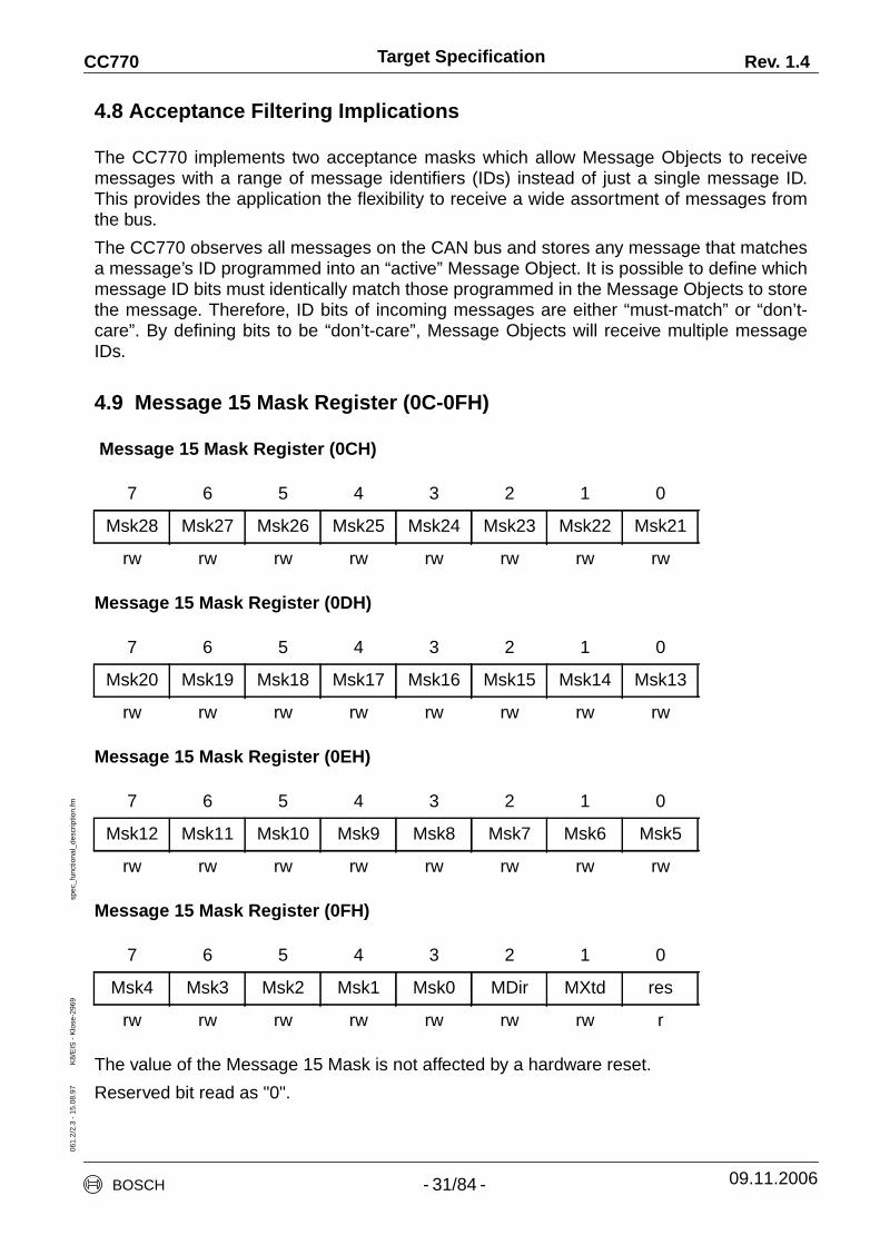
4.8 Acceptance Filtering Implications
The CC770 implements two acceptance masks which allow Message Objects to receivemessages with a range of message identifiers (IDs) instead of just a single message ID.This provides the application the flexibility to receive a wide assortment of messages fromthe bus.
The CC770 observes all messages on the CAN bus and stores any message that matchesa message’s ID programmed into an “active” Message Object. It is possible to define whichmessage ID bits must identically match those programmed in the Message Objects to storethe message. Therefore, ID bits of incoming messages are either “must-match” or “don’t-care”. By defining bits to be “don’t-care”, Message Objects will receive multiple messageIDs.
4.9 Message 15 Mask Register (0C-0FH)
Message 15 Mask Register (0CH)
Message 15 Mask Register (0DH)
Message 15 Mask Register (0EH)
Message 15 Mask Register (0FH)
The value of the Message 15 Mask is not affected by a hardware reset.
Reserved bit read as "0".
7 6 5 4 3 2 1 0
Msk28 Msk27 Msk26 Msk25 Msk24 Msk23 Msk22 Msk21
rw rw rw rw rw rw rw rw
7 6 5 4 3 2 1 0
Msk20 Msk19 Msk18 Msk17 Msk16 Msk15 Msk14 Msk13
rw rw rw rw rw rw rw rw
7 6 5 4 3 2 1 0
Msk12 Msk11 Msk10 Msk9 Msk8 Msk7 Msk6 Msk5
rw rw rw rw rw rw rw rw
7 6 5 4 3 2 1 0
Msk4 Msk3 Msk2 Msk1 Msk0 MDir MXtd res
rw rw rw rw rw rw rw r
BOSCH - 31/84 - 09.11.2006
Target Specification Rev. 1.4CC77006
1.2/
2.3
- 15
.08.
97
K8/
EIS
- K
lose
-296
9sp
ec_f
unct
iona
l_de
scrip
tion.
fm
Mskx Mask bit at position X
one must-match (incoming bit value must match to the corresponding bit in the Arbi-tration Register from the Message Object 15)
zero don’t care (accept a "0" or "1" for that bit position)
MDir Mask Direction Bit (EAF must be set, see note)
one must-match (incoming Direction bit value must match to the corresponding bitin the Arbitration Register from the Message Object 15)
zero don’t care (Message Object 15 accepts Remote and Data Frames)
MXtd Mask Extended Bit (EAF must be set, see note)
one must-match (incoming Xtd bit value must match to the corresponding bit in theArbitration Register from the Message Object 15)
zero don’t care (Message Object 15 accepts Standard and Extended IdentifierFrames)
Notes:
The Message 15 Mask Register is a programmable local mask. This feature allows the userto locally mask, or “don’t care”, any identifier bits of the incoming message for MessageObject 15. Incoming messages are first checked for an acceptance match in MessageObjects 1- 14 before passing through to Message Object 15. Consequently, the GlobalMask and the Local Mask apply to messages received in Message Object 15 in that way,that Message 15 Mask is “ANDed” with the Global Mask. This means that any bit defined as“don’t-care” in the Global Mask will automatically be a “don’t care” bit for message 15.
For the receive-only Message Object 15, it is also possible to mask the bits Dir and Xtd,allows the reception of Standard and Extended as well as Data and Remote Frames in thisMessage Object.
To enable the MDir and MXtd bits the EAF bit has to be set in the Control Register 00H.
If EAF="0", the additional mask bits MDir and MXtd in the Message 15 Mask Register aredisabled and the bits will be read as "00", independent of the last value written to those bitswhile EAF was set. The internal interpretation is "11", so the bits Dir and Xtd must match foracceptance filtering.
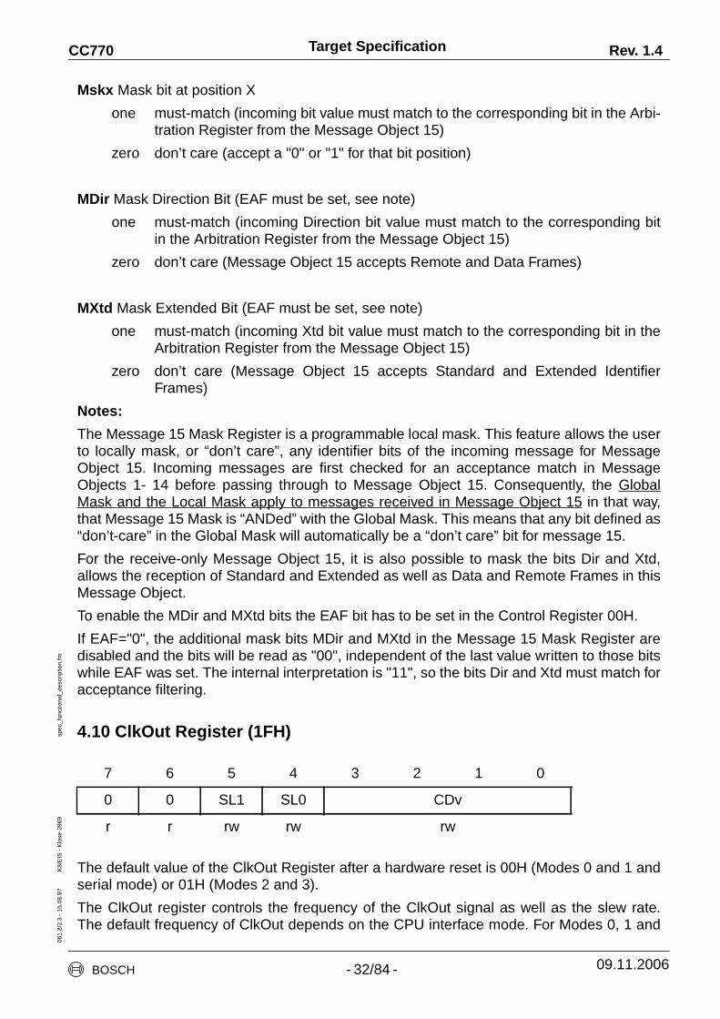
4.10 ClkOut Register (1FH)
The default value of the ClkOut Register after a hardware reset is 00H (Modes 0 and 1 andserial mode) or 01H (Modes 2 and 3).
The ClkOut register controls the frequency of the ClkOut signal as well as the slew rate.The default frequency of ClkOut depends on the CPU interface mode. For Modes 0, 1 and
7 6 5 4 3 2 1 0
0 0 SL1 SL0 CDv
r r rw rw rw
BOSCH - 32/84 - 09.11.2006
Target Specification Rev. 1.4CC77006
1.2/
2.3
- 15
.08.
97
K8/
EIS
- K
lose
-296
9sp
ec_f
unct
iona
l_de
scrip
tion.
fm
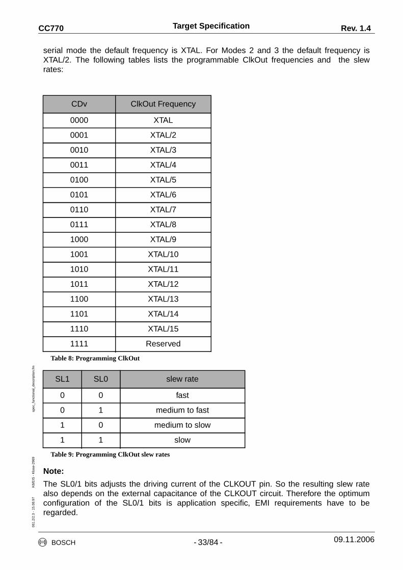
serial mode the default frequency is XTAL. For Modes 2 and 3 the default frequency isXTAL/2. The following tables lists the programmable ClkOut frequencies and the slewrates:
Note:
The SL0/1 bits adjusts the driving current of the CLKOUT pin. So the resulting slew ratealso depends on the external capacitance of the CLKOUT circuit. Therefore the optimumconfiguration of the SL0/1 bits is application specific, EMI requirements have to beregarded.
CDv ClkOut Frequency
0000 XTAL
0001 XTAL/2
0010 XTAL/3
0011 XTAL/4
0100 XTAL/5
0101 XTAL/6
0110 XTAL/7
0111 XTAL/8
1000 XTAL/9
1001 XTAL/10
1010 XTAL/11
1011 XTAL/12
1100 XTAL/13
1101 XTAL/14
1110 XTAL/15
1111 Reserved
Table 8: Programming ClkOut
SL1 SL0 slew rate
0 0 fast
0 1 medium to fast
1 0 medium to slow
1 1 slow
Table 9: Programming ClkOut slew rates
BOSCH - 33/84 - 09.11.2006
Target Specification Rev. 1.4CC77006
1.2/
2.3
- 15
.08.
97
K8/
EIS
- K
lose
-296
9sp
ec_f
unct
iona
l_de
scrip
tion.
fm
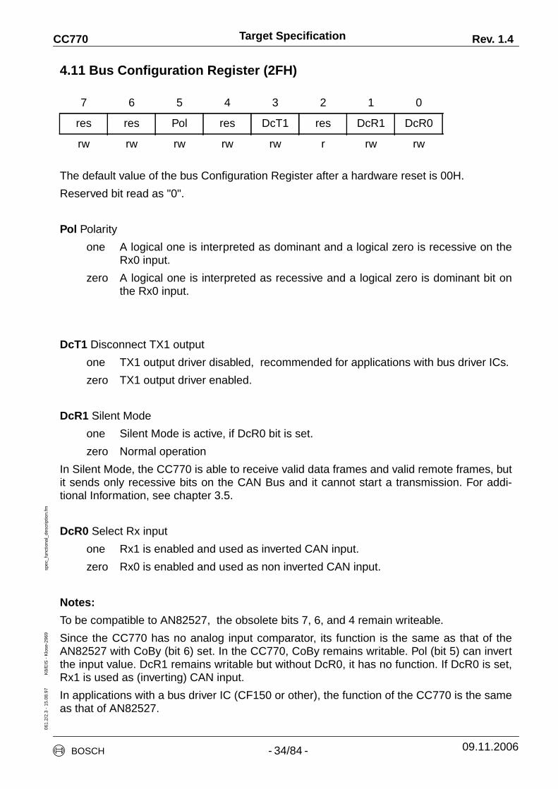
4.11 Bus Configuration Register (2FH)
The default value of the bus Configuration Register after a hardware reset is 00H.
Reserved bit read as "0".
Pol Polarity
one A logical one is interpreted as dominant and a logical zero is recessive on theRx0 input.
zero A logical one is interpreted as recessive and a logical zero is dominant bit onthe Rx0 input.
DcT1 Disconnect TX1 output
one TX1 output driver disabled, recommended for applications with bus driver ICs.
zero TX1 output driver enabled.
DcR1 Silent Mode
one Silent Mode is active, if DcR0 bit is set.
zero Normal operation
In Silent Mode, the CC770 is able to receive valid data frames and valid remote frames, butit sends only recessive bits on the CAN Bus and it cannot start a transmission. For addi-tional Information, see chapter 3.5.
DcR0 Select Rx input
one Rx1 is enabled and used as inverted CAN input.
zero Rx0 is enabled and used as non inverted CAN input.
Notes:
To be compatible to AN82527, the obsolete bits 7, 6, and 4 remain writeable.
Since the CC770 has no analog input comparator, its function is the same as that of theAN82527 with CoBy (bit 6) set. In the CC770, CoBy remains writable. Pol (bit 5) can invertthe input value. DcR1 remains writable but without DcR0, it has no function. If DcR0 is set,Rx1 is used as (inverting) CAN input.
In applications with a bus driver IC (CF150 or other), the function of the CC770 is the sameas that of AN82527.
7 6 5 4 3 2 1 0
res res Pol res DcT1 res DcR1 DcR0
rw rw rw rw rw r rw rw
BOSCH - 34/84 - 09.11.2006
Target Specification Rev. 1.4CC77006
1.2/
2.3
- 15
.08.
97
K8/
EIS
- K
lose
-296
9sp
ec_f
unct
iona
l_de
scrip
tion.
fm
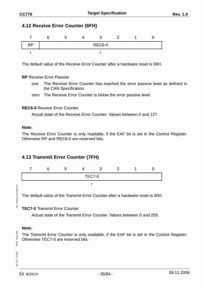
4.12 Receive Error Counter (6FH)
The default value of the Receive Error Counter after a hardware reset is 00H.
RP Receive Error Passive
one The Receive Error Counter has reached the error passive level as defined inthe CAN Specification.
zero The Receive Error Counter is below the error passive level.
REC6-0 Receive Error Counter
Actual state of the Receive Error Counter. Values between 0 and 127.
Note:
The Receive Error Counter is only readable, if the EAF bit is set in the Control Register.Otherwise RP and REC6-0 are reserved bits.
4.13 Transmit Error Counter (7FH)
The default value of the Transmit Error Counter after a hardware reset is 00H.
TEC7-0 Transmit Error Counter
Actual state of the Transmit Error Counter. Values between 0 and 255.
Note:
The Transmit Error Counter is only readable, if the EAF bit is set in the Control Register.Otherwise TEC7-0 are reserved bits.
7 6 5 4 3 2 1 0
RP REC6-0
r r
7 6 5 4 3 2 1 0
TEC7-0
r
BOSCH - 35/84 - 09.11.2006
Target Specification Rev. 1.4CC77006
1.2/
2.3
- 15
.08.
97
K8/
EIS
- K
lose
-296
9sp
ec_f
unct
iona
l_de
scrip
tion.
fm
4.14 Bit Timing Registers
4.14.1 Bit Timing Overview
A CAN message consists of a series of bits that are transmitted in consecutive bit times. Abit time accounts for propagation delay of the bit, CAN chip input and output delay, and syn-chronization tolerances. This section describes components of a bit time from the perspec-tive of the CAN Specification and the CC770.
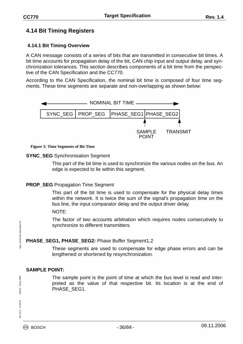
According to the CAN Specification, the nominal bit time is composed of four time seg-ments. These time segments are separate and non-overlapping as shown below:
Figure 3: Time Segments of Bit Time
SYNC_SEG Synchronisation Segment
This part of the bit time is used to synchronize the various nodes on the bus. Anedge is expected to lie within this segment.
PROP_SEG Propagation Time Segment
This part of the bit time is used to compensate for the physical delay timeswithin the network. It is twice the sum of the signal’s propagation time on thebus line, the input comparator delay and the output driver delay.
NOTE:
The factor of two accounts arbitration which requires nodes consecutively tosynchronize to different transmitters.
PHASE_SEG1, PHASE_SEG2: Phase Buffer Segment1,2
These segments are used to compensate for edge phase errors and can belengthened or shortened by resynchronization.
SAMPLE POINT:
The sample point is the point of time at which the bus level is read and inter-preted as the value of that respective bit. Its location is at the end ofPHASE_SEG1.
SYNC_SEG
SAMPLE TRANSMIT
NOMINAL BIT TIME
PHASE_SEG2PHASE_SEG1PROP_SEG
POINT
BOSCH - 36/84 - 09.11.2006
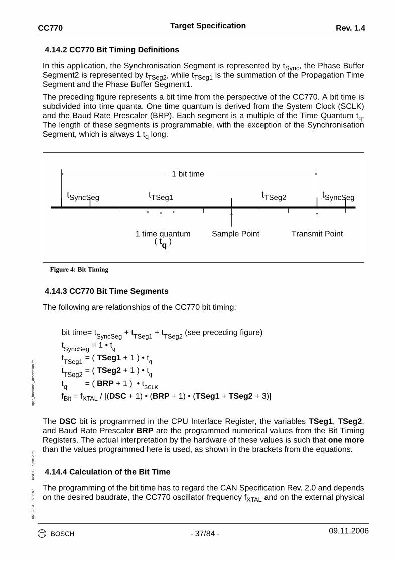
Target Specification Rev. 1.4CC77006
1.2/
2.3
- 15
.08.
97
K8/
EIS
- K
lose
-296
9sp
ec_f
unct
iona
l_de
scrip
tion.
fm
4.14.2 CC770 Bit Timing Definitions
In this application, the Synchronisation Segment is represented by tSync, the Phase BufferSegment2 is represented by tTSeg2, while tTSeg1 is the summation of the Propagation TimeSegment and the Phase Buffer Segment1.
The preceding figure represents a bit time from the perspective of the CC770. A bit time issubdivided into time quanta. One time quantum is derived from the System Clock (SCLK)and the Baud Rate Prescaler (BRP). Each segment is a multiple of the Time Quantum tq.The length of these segments is programmable, with the exception of the SynchronisationSegment, which is always 1 tq long.
Figure 4: Bit Timing
4.14.3 CC770 Bit Time Segments
The following are relationships of the CC770 bit timing:
bit time= tSyncSeg + tTSeg1 + tTSeg2 (see preceding figure)
tSyncSeg = 1 • tqtTSeg1 = ( TSeg1 + 1 ) • tqtTSeg2 = ( TSeg2 + 1 ) • tqtq = ( BRP + 1 ) • tSCLK
fBit = fXTAL / [(DSC + 1) • (BRP + 1) • (TSeg1 + TSeg2 + 3)]
The DSC bit is programmed in the CPU Interface Register, the variables TSeg1, TSeg2,and Baud Rate Prescaler BRP are the programmed numerical values from the Bit TimingRegisters. The actual interpretation by the hardware of these values is such that one morethan the values programmed here is used, as shown in the brackets from the equations.
4.14.4 Calculation of the Bit Time
The programming of the bit time has to regard the CAN Specification Rev. 2.0 and dependson the desired baudrate, the CC770 oscillator frequency fXTAL and on the external physical
tSyncSeg tSyncSegtTSeg1 tTSeg2
1 bit time
1 time quantum( tq )
Sample Point Transmit Point
BOSCH - 37/84 - 09.11.2006

Target Specification Rev. 1.4CC77006
1.2/
2.3
- 15
.08.
97
K8/
EIS
- K
lose
-296
9sp
ec_f
unct
iona
l_de
scrip
tion.
fm
delay times of the bus driver, of the bus line and of the input comparator. The delay timesare summarised in the Propagation Time Segment, its actual value tProp is:
tProp is two times the maximum of the sum of physical bus delay, the input compara-tor delay, and the output driver delay rounded up to the nearest multiple of tq.
To fulfil the requirements of the CAN specification, the following conditions must be met :
tTSeg2 ≥ 1 • tq = Information Processing Time
tTSeg2 ≥ tSJWtTSeg1 ≥ 2 • tqtTSeg1 ≥ tSJW + tProptTSeg1 ≥ tSJW + tProp + 2tq for 3 Sample Mode (bit Spl="1" in register 4FH)
Note:
In order to achieve correct operation according to the CAN protocol the total bit time shouldbe at least 8 tq, i.e. TSeg1 + TSeg2 ≥ 5 (as programmed in the Bit Timing Register 1).
To operate with a baudrate of 1 MBit/s, the frequency of SCLK has to be at least 8 MHz, inconsequence fXTAL has to be at least 16 MHz.
The maximum tolerance df for XTAL depends on the Phase Buffer Segment1 (PB1), thePhase Buffer Segment2 (PB2), and the Resynchronisation Jump Width (SJW):
df ≤AND
df ≤
(PB1 = tTSeg1 - tProp ; PB2 = tTSeg2)
min PB1 PB2,( )2 13 bit time PB2–×( )×-----------------------------------------------------------------
SJW20 bit time×--------------------------------
BOSCH - 38/84 - 09.11.2006

Target Specification Rev. 1.4CC77006
1.2/
2.3
- 15
.08.
97
K8/
EIS
- K
lose
-296
9sp
ec_f
unct
iona
l_de
scrip
tion.
fm
4.14.5 Example for Bit Timing at high Baudrate
Configuration:
fXTAL = 20 MHz, fSCLK = 10MHz (DSC=1), BRP = 0, bitrate should be 1 MBit/s.
tq 100 ns = tSCLK = tXTAL • 2
delay of bus driver 50 nsdelay of receiver circuit 30 nsdelay of bus line (40m) 220 ns = 520 ns, round up ↵tProp 600 ns = 6 • tqtSJW 100 ns = 1 • tqtTSeg1 700 ns = tProp + tSJW
tTSeg2 200 ns = Information Processing Time + 1 • tqtSync-Seg 100 ns = 1 • tq (fix)
bit time 1000 ns = tSync-Seg + tTSeg1 + tTSeg2
maximal oscillator tolerance 0.39 % =
=
In this example, the Bit Timing Registers must be programmed with the following values:
Bit Timing Register 0 (3FH): 00H
Bit Timing Register 1 (4FH): 16H
4.14.6 Bit Timing Registers 0 + 1 (3FH + 4FH)
Bit Timing Registers are used to define the CAN bus frequency, the sample point within abit time, and the mode of synchronization.
Bit Timing Register 0 (3FH)
The default value of the Bit Timing Register 0 after a hardware reset is 00H.
SJW (Re) Synchronization Jump Width
The valid programmed values are 0-3. The SJW defines the maximum numberof time quanta a bit time may be shortened or lengthened by one resynchroni-zation.
The actual interpretation of this value by the hardware is to use one more thanthe programmed value.
7 6 5 4 3 2 1 0
SJW BRP
rw rw
min PB1 PB2,( )2 13 bit time PB2–×( )×----------------------------------------------------------------
0.1µs2 13 1µs 0.2µs–×( )×-----------------------------------------------------------
BOSCH - 39/84 - 09.11.2006

Target Specification Rev. 1.4CC77006
1.2/
2.3
- 15
.08.
97
K8/
EIS
- K
lose
-296
9sp
ec_f
unct
iona
l_de
scrip
tion.
fm
BRP Baud Rate Prescaler
The valid programmed values are 0-63. The baud rate prescaler programs thelength of one time quantum as follows: tq = tSCLK • (BRP + 1) where tSCLK is theperiod of the system clock (SCLK).
Bit Timing Register 1 (4FH)
The default value of the Bit Timing Register 1 after a hardware reset is 00H.
Spl Sampling Mode
one The CAN bus is sampled three times per bit time for determining the valid bitvalue using majority logic.
zero Bus is sampled once, may result in faster bit transmissions rates.
Sampling mode = "0" may result in faster bit transmissions rates, while sampling mode = "1"is more immune to noise spikes on the CAN bus.
TSeg2 Time Segment 2
The valid programmed values are 0-7. TSeg2 is the time segment after thesample point.
The actual interpretation of this value by the hardware is one more than thevalue programmed by the user.
TSeg1 Time Segment 1
The valid programmed values are 1-15. TSeg1 is the time segment before thesample point.
The actual interpretation of this value by the hardware is one more than thevalue programmed by the user.
4.15 Interrupt Register (5FH)
The default value of the Interrupt Register after a hardware reset is 00H.
7 6 5 4 3 2 1 0
Spl TSeg2 TSeg1
rw rw rw
7 6 5 4 3 2 1 0
IntId
r
BOSCH - 40/84 - 09.11.2006
Target Specification Rev. 1.4CC77006
1.2/
2.3
- 15
.08.
97
K8/
EIS
- K
lose
-296
9sp
ec_f
unct
iona
l_de
scrip
tion.
fm
IntId Interrupt Identifier
The Interrupt Register is a read-only register. The value in this register indicates the sourceof the interrupt. When no interrupt is pending, this register holds the value "0". If the SIE bitin the Control Register (00H) is set and the CC770 has updated the Status Register, theInterrupt Register will contain a "1". This indicates an interrupt is pending due to a changein the Status Register. The value 2 + Message Object Number indicates the IntPnd bit in thecorresponding Message Object is set. There is an exception in that Message Object 15 willhave the value 2, giving Message Object 15 the highest priority of all Message Objects.
For example, a message is received by Message Object 13 with the IE (Control Register)and RxIE (Message Object 13 Control 0 Register) bits set. The interrupt pin will be pulledlow and the value 15 (0FH) will be placed in the Interrupt Register.
If the value of the Interrupt Register equals "1", then the Status Register at location 01Hmust be read to update this Interrupt Register. The Status Change Interrupt has a higherpriority than interrupts from the Message Objects. Register 5FH is automatically set to "0"or to the lowest value corresponding to a Message Object with IntPnd set. When the valueof this register is two or more, the IntPnd bit of the corresponding Message Object ControlRegister is set.
Interrupt Source Value
none 00H
Status Register 01H
Message Object 15 02H
Message Object 1 03H
Message Object 2 04H
Message Object 3 05H
Message Object 4 06H
Message Object 5 07H
Message Object 6 08H
Message Object 7 09H
Message Object 8 0AH
Message Object 9 0BH
Message Object 10 0CH
Message Object 11 0DH
Message Object 12 0EH
Message Object 13 0FH
Message Object 14 10H
Table 10: Interrupt Register values with corresponding Interrupt Sources
BOSCH - 41/84 - 09.11.2006
Target Specification Rev. 1.4CC77006
1.2/
2.3
- 15
.08.
97
K8/
EIS
- K
lose
-296
9sp
ec_f
unct
iona
l_de
scrip
tion.
fm
The CC770 will respond to each status change event independently and will not bundleinterrupt events in a single interrupt signal. However, if two status change events occurbefore the first is acknowledged by the CPU, the next event will not generate a separateinterrupt output. Therefore, when servicing Status Change Interrupts, the user code shouldcheck all useful status bits upon each Status Change Interrupt.
After resetting the IntPnd bit in the Control 0 Register of individual Message Objects, theminimum delay of the CC770 resetting the interrupt pin and updating the Interrupt Register(5FH) is 3 MCLK cycles and a maximum of 14 MCLK cycles (after the CPU write operationto this register is finished). When a Status Change Interrupt occurs, reading the StatusRegister (01H) will reset the interrupt pin in a maximum of 4 MCLK cycles + 145 ns. Clear-ing the IntPnd bit of the Message Object will deactivate the INT# pin.
4.16 Serial Reset Address (FFH)
The serial reset address is used to synchronize accesses between the CC770 and theCPU.
For example the CPU cannot provide a chip select signal, it is possible to write as manyones into the CC770 SPI until you get the value "AAH" from the MISO pin. Then the CC770is synchronized and data transfer could be started. For further informations see chapter 7.4.
4.17 CC770 Message Objects (MO)
4.17.1 Message Object Structure
The Message Object is the means of communication between the host microcontoller andthe CAN controller in the CC770. Message Objects are configured to transmit or receivemessages.
There are 15 Message Objects located at fixed addresses in the CC770. Each MessageObject starts at a base address that is a multiple of 16 bytes and uses 15 consecutivebytes. For example, Message Object 1 starts at address 10H and ends at address 1EH.The remaining byte in the 16 byte field is used for other CC770 functions. In the aboveexample the byte at address 1FH is used for the ClkOut register.
Message Object 15 is a receive-only Message Object that uses a local mask called theMessage 15 Mask Register. This mask allows a large number of infrequent messages to bereceived by the CC770. In addition, Message Object 15 is buffered to allow the CPU moretime to receive messages.
7 6 5 4 3 2 1 0
Serial Reset Address
w
BOSCH - 42/84 - 09.11.2006

Target Specification Rev. 1.4CC77006
1.2/
2.3
- 15
.08.
97
K8/
EIS
- K
lose
-296
9sp
ec_f
unct
iona
l_de
scrip
tion.
fm
4.17.2 Control 0 + 1 Registers
Control 0 Register (Base Address + 0)
Control 1 Register (Base Address + 1)
The values of the Control 0 and Control 1 registers are not affected by a hardware reset.
Address Function
Base Address +0 Control 0
+1 Control 1
+2 Arbitration 0
+3 Arbitration 1
+4 Arbitration 2
+5 Arbitration 3
+6 Configuration
+7 Data 0
+8 Data 1
+9 Data 2
+10 Data 3
+11 Data 4
+12 Data 5
+13 Data 6
+14 Data 7
Table 11: Message Object Structure
7 6 5 4 3 2 1 0
MsgVal TxIE RxIE IntPnd
rw rw rw rw
7 6 5 4 3 2 1 0
RmtPnd TxRqst MsgLst/CPUUpd NewDat
rw rw rw rw
BOSCH - 43/84 - 09.11.2006
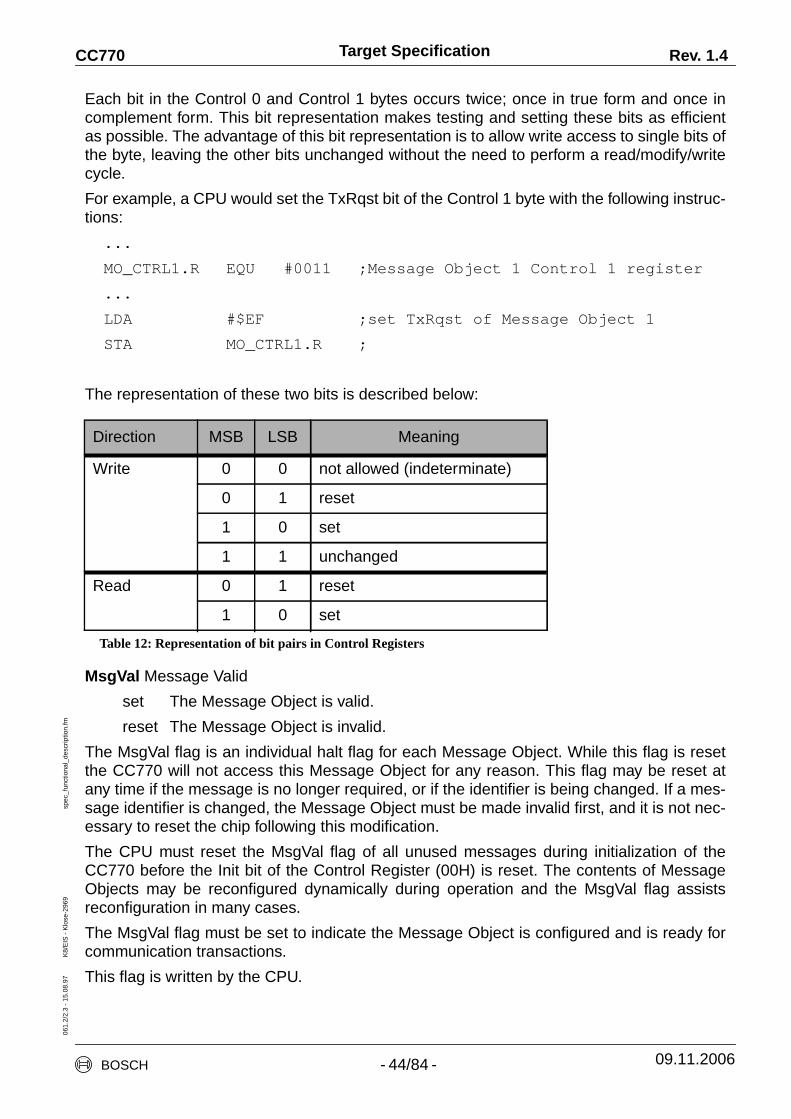
Target Specification Rev. 1.4CC77006
1.2/
2.3
- 15
.08.
97
K8/
EIS
- K
lose
-296
9sp
ec_f
unct
iona
l_de
scrip
tion.
fm
Each bit in the Control 0 and Control 1 bytes occurs twice; once in true form and once incomplement form. This bit representation makes testing and setting these bits as efficientas possible. The advantage of this bit representation is to allow write access to single bits ofthe byte, leaving the other bits unchanged without the need to perform a read/modify/writecycle.
For example, a CPU would set the TxRqst bit of the Control 1 byte with the following instruc-tions:
...
MO_CTRL1.R EQU #0011 ;Message Object 1 Control 1 register
...
LDA #$EF ;set TxRqst of Message Object 1
STA MO_CTRL1.R ;
The representation of these two bits is described below:
MsgVal Message Valid
set The Message Object is valid.
reset The Message Object is invalid.
The MsgVal flag is an individual halt flag for each Message Object. While this flag is resetthe CC770 will not access this Message Object for any reason. This flag may be reset atany time if the message is no longer required, or if the identifier is being changed. If a mes-sage identifier is changed, the Message Object must be made invalid first, and it is not nec-essary to reset the chip following this modification.
The CPU must reset the MsgVal flag of all unused messages during initialization of theCC770 before the Init bit of the Control Register (00H) is reset. The contents of MessageObjects may be reconfigured dynamically during operation and the MsgVal flag assistsreconfiguration in many cases.
The MsgVal flag must be set to indicate the Message Object is configured and is ready forcommunication transactions.
This flag is written by the CPU.
Direction MSB LSB Meaning
Write 0 0 not allowed (indeterminate)
0 1 reset
1 0 set
1 1 unchanged
Read 0 1 reset
1 0 set
Table 12: Representation of bit pairs in Control Registers
BOSCH - 44/84 - 09.11.2006

Target Specification Rev. 1.4CC77006
1.2/
2.3
- 15
.08.
97
K8/
EIS
- K
lose
-296
9sp
ec_f
unct
iona
l_de
scrip
tion.
fm
IMPORTANT NOTE:
Two or more Message Objects must not have the same message identifier and also be validat the same time!
If more than one CC770 transmit Message Object has the same message ID, a successfultransmission of the higher numbered Message Objects will not be recognized by theCC770. The lower numbered Message Object will be falsely identified as the transmit Mes-sage Object and its transmit request flag will be reset. The actual transmit Message Objectwill re-transmit without end because its transmit request flag will not be reset.
This could result in a catastrophic condition since the higher numbered Message Objectmay dominate the CAN bus by resending its message without end.
To avoid this condition, applications should require all transmit Message Objects to usemessage IDs that are unique. If this is not possible, the application should disable lowernumbered Message Objects with similar message IDs until the higher numbered MessageObject has transmitted successfully.
TxIE Transmit Interrupt Enable
set An interrupt will be generated after a successful transmission of a frame.
reset No interrupt will be generated after a successful transmission of a frame.
The Transmit Interrupt Enable flag enables the CC770 to initiate an interrupt after the suc-cessful transmission by the corresponding Message Object.
This flag is written by the CPU.
RxIE Receive Interrupt Enable
set An interrupt will be generated after a successful reception of a frame.
reset No interrupt will be generated after a successful reception of a frame.
This flag enables the CC770 to initiate an interrupt after the successful reception by the cor-responding Message Object.
This flag is written by the CPU.
NOTE:
In order for TxIE or RxIE to generate an interrupt, IE in the Control Register must be set.
IntPnd Interrupt Pending
set This Message Object has generated an interrupt.
reset No interrupt was generated by this Message Object since the last time the CPUcleared this flag.
This flag is set by the CC770 following a successful transmission or reception as controlledby the RxIE and TxIE flags.
The CPU must clear this flag when servicing the interrupt.
BOSCH - 45/84 - 09.11.2006

Target Specification Rev. 1.4CC77006
1.2/
2.3
- 15
.08.
97
K8/
EIS
- K
lose
-296
9sp
ec_f
unct
iona
l_de
scrip
tion.
fm
RmtPnd Remote Request Pending
set The transmission of this Message Object has been requested by a remotenode and is not yet done.
reset There is no waiting remote request for the Message Object.
This flag is only used by Message Objects with direction = transmit. This flag is set by theCC770 after receiving a remote frame which matches its message identifier, taking intoaccount the Global Mask Register. The corresponding Message Object will respond bytransmitting a message, if the CPUUpd flag is reset. Following this transmission, the CC770will clear the RmtPnd flag. In other words, when this flag is set it indicates a remote nodehas requested data and this request is still pending because the data has not yet beentransmitted.
NOTE:
Setting RmtPnd will not cause a remote frame to be transmitted. The TxRqst flag is used tosend a remote frame from a receive Message Object.
TxRqst Transmit Request
set The transmission of this Message Object has been requested and has not beencompleted.
reset This Message Object is not waiting to be transmitted.
This flag is set by the CPU to indicate the Message Object data should be transmitted. Set-ting TxRqst will send a data frame for a transmit Message Object and a remote frame for areceive Message Object.
If direction = receive a remote frame is sent to request a remote node to send the corre-sponding data.
TxRqst is also set by the CC770 (at the same time as RmtPnd in Message Objects whosedirection = transmit) when it receives a remote frame from another node requesting thisdata. This flag is cleared by the CC770 along with RmtPnd when the message has beensuccessfully transmitted, if the NewDat flag has not been set.
MsgLst Message Lost
Only valid for Message Objects with direction = receive.
set The CC770 has stored a new message in this Message Object when NewDatwas still set.
reset No message was lost since the last time this flag was reset by the CPU.
This flag is used to signal that the CC770 stored a new message into this Message Objectwhen the NewDat flag was still set. Therefore, this flag is set if the CPU did not process thecontents of this Message Object since the last time the CC770 set the NewDat flag; thisindicates the last message received by this Message Object overwrote the previous mes-sage which was not read and is lost.
This definition is only valid for Message Objects with direction = receive. For MessageObjects with direction = transmit, the definition is replaced by CPUUpd.
BOSCH - 46/84 - 09.11.2006

Target Specification Rev. 1.4CC77006
1.2/
2.3
- 15
.08.
97
K8/
EIS
- K
lose
-296
9sp
ec_f
unct
iona
l_de
scrip
tion.
fm
CPUUpd CPU Updating
Only valid for Message Objects with direction = transmit.
set This Message Object may not be transmitted.
reset This Message Object may be transmitted, if direction = transmit.
The CPU sets this flag to indicate it is updating the data contents of the Message Objectand the message should not be transmitted until this flag has been reset. The CPU indi-cates message updating has been completed by resetting this flag (it is not necessary touse the MsgVal flag to update the Message Object’s data contents).
The purpose of this flag is to prevent a remote frame from triggering a transmission ofinvalid data.
NewDat New Data
set The CC770 or CPU has written new data into the data section of this MessageObject.
reset No new data has been written into the data section of this Message Objectsince the last time this flag was cleared by the CPU.
This flag has different meanings for receive and transmit Message Objects.
4.17.3 Handling of Message Objects
For Message Objects with direction = receive, the CC770 sets the NewDat flag whenevernew data has been written into the Message Object.
When the received data is written into Message Objects 1-14, the unused data bytes will beoverwritten with non-specified values.
The CPU should clear the NewDat flag before reading the received data and then check ifthe flag remained cleared when all bytes have been read. If the NewDat flag is set, the CPUshould re-read the received data to prevent working with a combination of old and newdata. See flow diagram in chapter 6.4.
When the received Data is matched to Message Object 15, new data is written into theshadow register. The foreground register is not over-written with new data. For MessageObject 15 messages, the data should be read first, the IntPnd reset, and then the NewDatand RmtPnd flags are reset. Resetting the NewDat and RmtPnd flags before resetting theIntPnd flag will result the interrupt line remaining active. See flow diagram in chapter 6.5.
For Message Objects with direction = transmit, the CPU should set the NewDat flag toindicate it has updated the message contents. This is done at the same time the CPUclears the CPUUpd flag. This will ensure that if the message is actually being transmittedduring the time the message was being updated by the CPU, the CC770 will not reset theTxRqst flag. In this way, the TxRqst flag is reset only after the actual data has been trans-ferred. See flow diagram in chapter 6.3.
Each flag in the Control 0 and Control 1 registers may be set and reset by the CPU asrequired.
BOSCH - 47/84 - 09.11.2006
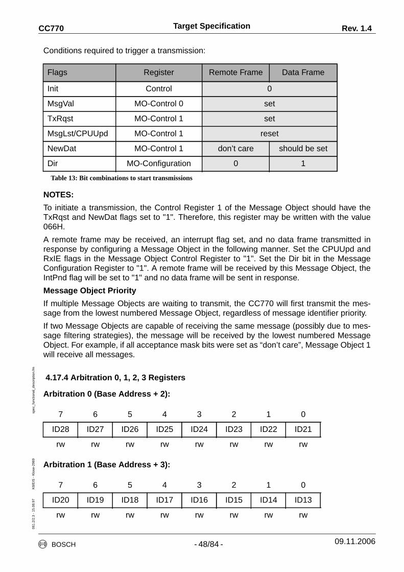
Target Specification Rev. 1.4CC77006
1.2/
2.3
- 15
.08.
97
K8/
EIS
- K
lose
-296
9sp
ec_f
unct
iona
l_de
scrip
tion.
fm
Conditions required to trigger a transmission:
NOTES:
To initiate a transmission, the Control Register 1 of the Message Object should have theTxRqst and NewDat flags set to "1". Therefore, this register may be written with the value066H.
A remote frame may be received, an interrupt flag set, and no data frame transmitted inresponse by configuring a Message Object in the following manner. Set the CPUUpd andRxIE flags in the Message Object Control Register to "1". Set the Dir bit in the MessageConfiguration Register to "1". A remote frame will be received by this Message Object, theIntPnd flag will be set to "1" and no data frame will be sent in response.
Message Object Priority
If multiple Message Objects are waiting to transmit, the CC770 will first transmit the mes-sage from the lowest numbered Message Object, regardless of message identifier priority.
If two Message Objects are capable of receiving the same message (possibly due to mes-sage filtering strategies), the message will be received by the lowest numbered MessageObject. For example, if all acceptance mask bits were set as “don’t care”, Message Object 1will receive all messages.
4.17.4 Arbitration 0, 1, 2, 3 Registers
Arbitration 0 (Base Address + 2):
Arbitration 1 (Base Address + 3):
Flags Register Remote Frame Data Frame
Init Control 0
MsgVal MO-Control 0 set
TxRqst MO-Control 1 set
MsgLst/CPUUpd MO-Control 1 reset
NewDat MO-Control 1 don’t care should be set
Dir MO-Configuration 0 1
Table 13: Bit combinations to start transmissions
7 6 5 4 3 2 1 0
ID28 ID27 ID26 ID25 ID24 ID23 ID22 ID21
rw rw rw rw rw rw rw rw
7 6 5 4 3 2 1 0
ID20 ID19 ID18 ID17 ID16 ID15 ID14 ID13
rw rw rw rw rw rw rw rw
BOSCH - 48/84 - 09.11.2006
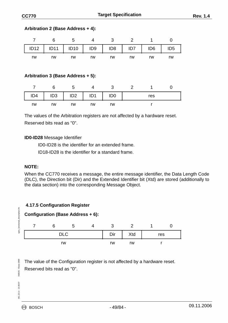
Target Specification Rev. 1.4CC77006
1.2/
2.3
- 15
.08.
97
K8/
EIS
- K
lose
-296
9sp
ec_f
unct
iona
l_de
scrip
tion.
fm
Arbitration 2 (Base Address + 4):
Arbitration 3 (Base Address + 5):
The values of the Arbitration registers are not affected by a hardware reset.
Reserved bits read as "0".
ID0-ID28 Message Identifier
ID0-ID28 is the identifier for an extended frame.
ID18-ID28 is the identifier for a standard frame.
NOTE:
When the CC770 receives a message, the entire message identifier, the Data Length Code(DLC), the Direction bit (Dir) and the Extended Identifier bit (Xtd) are stored (additionally tothe data section) into the corresponding Message Object.
4.17.5 Configuration Register
Configuration (Base Address + 6):
The value of the Configuration register is not affected by a hardware reset.
Reserved bits read as "0".
7 6 5 4 3 2 1 0
ID12 ID11 ID10 ID9 ID8 ID7 ID6 ID5
rw rw rw rw rw rw rw rw
7 6 5 4 3 2 1 0
ID4 ID3 ID2 ID1 ID0 res
rw rw rw rw rw r
7 6 5 4 3 2 1 0
DLC Dir Xtd res
rw rw rw r
BOSCH - 49/84 - 09.11.2006
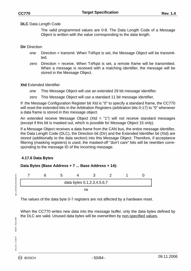
Target Specification Rev. 1.4CC77006
1.2/
2.3
- 15
.08.
97
K8/
EIS
- K
lose
-296
9sp
ec_f
unct
iona
l_de
scrip
tion.
fm
DLC Data Length Code
The valid programmed values are 0-8. The Data Length Code of a MessageObject is written with the value corresponding to the data length.
Dir Direction
one Direction = transmit. When TxRqst is set, the Message Object will be transmit-ted.
zero Direction = receive. When TxRqst is set, a remote frame will be transmitted.When a message is received with a matching identifier, the message will bestored in the Message Object.
Xtd Extended Identifier
one This Message Object will use an extended 29 bit message identifier.
zero This Message Object will use a standard 11 bit message identifier.
If the Message Configuration Register bit Xtd is "0" to specify a standard frame, the CC770will reset the extended bits in the Arbitration Registers (arbitration bits 0-17) to "0" whenevera data frame is stored in this message object.
An extended receive Message Object (Xtd = "1") will not receive standard messages(except if this bit is masked out, which is possible for Message Object 15 only).
If a Message Object receives a data frame from the CAN bus, the entire message identifier,the Data Length Code (DLC), the Direction bit (Dir) and the Extended Identifier bit (Xtd) arestored (additionally to the data section) into this Message Object. Therefore, if acceptancefiltering (masking registers) is used, the masked-off "don’t care" bits will be rewritten corre-sponding to the message ID of the incoming message.
4.17.6 Data Bytes
Data Bytes (Base Address + 7 ... Base Address + 14):
The values of the data byte 0-7 registers are not affected by a hardware reset.
When the CC770 writes new data into the message buffer, only the data bytes defined bythe DLC are valid. Unused data bytes will be overwritten by non-specified values.
7 6 5 4 3 2 1 0
data bytes 0,1,2,3,4,5,6,7
rw
BOSCH - 50/84 - 09.11.2006

Target Specification Rev. 1.4CC77006
1.2/
2.3
- 15
.08.
97
K8/
EIS
- K
lose
-296
9sp
ec_f
unct
iona
l_de
scrip
tion.
fm
4.18 Special Treatment of Message Object 15
Message Object 15 is a receive-only Message Object with a programmable local maskcalled the Message 15 Mask Register. Since this Message Object is a receive only Mes-sage Object, the TxRqst and the TxIE flags have been hardwired inactive and the CPUUpdflag has no meaning.
The incoming messages for Message Object 15 will be written into a two-message alternat-ing buffers to avoid the loss of a message if a second message is received before the CPUhas read the first message. Once Message Object 15 is read, it is necessary to reset theNewDat and the RmtPnd flags to allow the CPU to read the shadow message buffer whichwill receive the next message or which may already contain a new message.
If two messages have been received by Message Object 15, the first will be accessible tothe CPU. The alternate buffer will be overwritten if a subsequent (third receive) message isreceived. Once again, after reading message 15, the user program should reset the IntPndflag followed by a reset of the NewDat and RmtPnd flags in the Message Object ControlRegisters.
The Xtd bit in the Message Configuration Register determines whether a standard or anextended frame will be received by this Message Object. This bit could be masked out, seechapter 4.9.
BOSCH - 51/84 - 09.11.2006
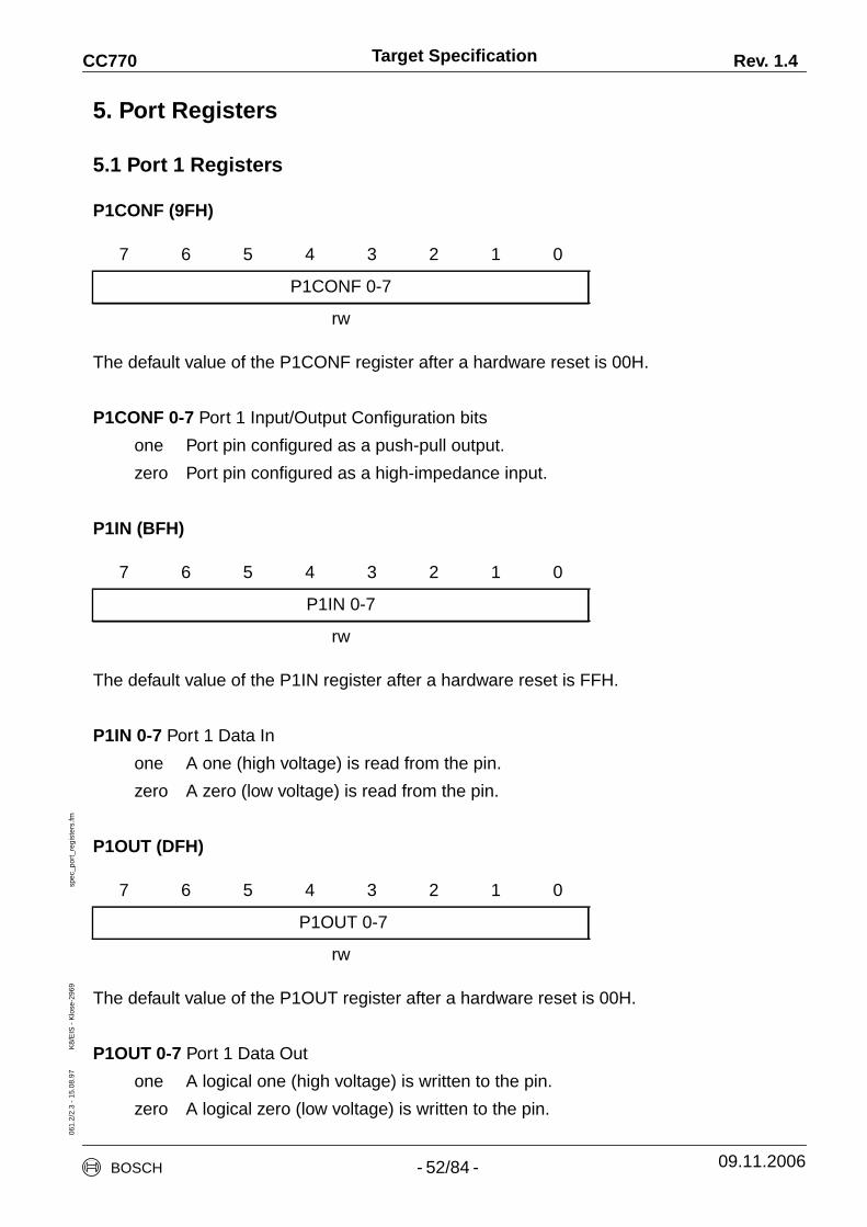
Target Specification Rev. 1.4CC77006
1.2/
2.3
- 15
.08.
97
K8/
EIS
- K
lose
-296
9sp
ec_p
ort_
regi
ster
s.fm
5. Port Registers
5.1 Port 1 Registers
P1CONF (9FH)
The default value of the P1CONF register after a hardware reset is 00H.
P1CONF 0-7 Port 1 Input/Output Configuration bits
one Port pin configured as a push-pull output.
zero Port pin configured as a high-impedance input.
P1IN (BFH)
The default value of the P1IN register after a hardware reset is FFH.
P1IN 0-7 Port 1 Data In
one A one (high voltage) is read from the pin.
zero A zero (low voltage) is read from the pin.
P1OUT (DFH)
The default value of the P1OUT register after a hardware reset is 00H.
P1OUT 0-7 Port 1 Data Out
one A logical one (high voltage) is written to the pin.
zero A logical zero (low voltage) is written to the pin.
7 6 5 4 3 2 1 0
P1CONF 0-7
rw
7 6 5 4 3 2 1 0
P1IN 0-7
rw
7 6 5 4 3 2 1 0
P1OUT 0-7
rw
BOSCH - 52/84 - 09.11.2006spec_port_registers.fm

Target Specification Rev. 1.4CC77006
1.2/
2.3
- 15
.08.
97
K8/
EIS
- K
lose
-296
9sp
ec_p
ort_
regi
ster
s.fm
5.2 Port 2 Registers
P2CONF (AFH)
The default value of the P2CONF register after a hardware reset is 00H.
P2CONF 0-7 Port 2 Input/Output Configuration bits
one Port pin configured as a push-pull output.
zero Port pin configured as a high-impedance input.
P2IN (CFH)
The default value of the P2IN register after a hardware reset is FFH.
P2IN 0-7 Port 2 Data In
one A one (high voltage) is read from the pin.
zero A zero (low voltage) is read from the pin.
P2OUT (EFH)
The default value of the P2OUT register after a hardware reset is 00H.
P2OUT 0-7 Port 2 Data Out
one A logical one (high voltage) is written to the pin.
zero A logical zero (low voltage) is written to the pin.
7 6 5 4 3 2 1 0
P2CONF 0-7
rw
7 6 5 4 3 2 1 0
P2IN 0-7
rw
7 6 5 4 3 2 1 0
P2OUT 0-7
rw
BOSCH - 53/84 - 09.11.2006

Target Specification Rev. 1.4CC77006
1.2/
2.3
- 15
.08.
97
K8/
EIS
- K
lose
-296
9sp
ec_f
low
_dia
gram
s.fm
6. FLOW DIAGRAMS
The following flowcharts describe the operation of the CC770 and suggested flows for thehost-CPU.
6.1 CC770 handling of Message Objects 1-14 (Transmit)
These are the operations the CC770 executes to transmit Message Objects. This diagramis useful to identify when the CC770 sets bits in the Control Registers.
Figure 5: CC770 handling of Message Objects 1-14 (Transmit)
bus free ?
NewDat := 0load message
into shift register
transmissionsuccessful?
NewDat=1TxRqst := 0
IntPnd := 1
send message
yes
no
yes
yes
yes
yes
yes
no
no
no
TxRqst := 1RmtPnd := 1
no
no
IntPnd := 1
yes
noRxIE = 1
TxRqst=1
TxIE = 1
received remote framewith matching identifier ?
DATA REMOTE
CPUUpd=0
RmtPnd := 0
BOSCH - 54/84 - 09.11.2006spec_flow_diagrams.fm

Target Specification Rev. 1.4CC77006
1.2/
2.3
- 15
.08.
97
K8/
EIS
- K
lose
-296
9sp
ec_f
low
_dia
gram
s.fm
6.2 CC770 handling of Message Objects 1-14 (Receive)
These are the operations the CC770 executes to receive Message Objects. This diagram isuseful to identify when the CC770 sets bits in the Control Registers.
Figure 6: CC770 handling of Message Objects 1-14 (Direction = Receive)
bus idle ?
TxRqst=1
NewDat := 0load identifier and
control into shift register
transmissionsuccessful?
TxRqst := 0RmtPnd := 0
TxIE = 1
IntPnd := 1
send remote frame
yes
no
yes
yes
yes
yes
no
no
store message
no
TxIE = 1
IntPnd := 1
yes
no
RmtPnd := 0
no
NewDat = 1
no MsgLst := 1
yes
TxRqst := 0NewDat := 1
received frame withmatching identifier to this
message object ?
REMOTE DATA
MsgLst =0
BOSCH - 55/84 - 09.11.2006

Target Specification Rev. 1.4CC77006
1.2/
2.3
- 15
.08.
97
K8/
EIS
- K
lose
-296
9sp
ec_f
low
_dia
gram
s.fm
6.3 CPU Handling of Message Objects 1-14 (Transmit)
These are the operations the host-CPU executes to transmit Message Objects 1-14.
Table 14: CPU Handling of Message Objects 1-14 (Transmit)
Power Up ( reset values )
want to sent ?
CPUUpd := 0
yes
CPUUpd := 1
write data bytes
no
Update Data Field
Initialisation
TxIE := ( application specific )RxIE := ( application specific )IntPnd := 0RmtPnd := 0TxRqst := 0CPUUpd := 1
Identifier := ( application specific )DLC := ( application specific )Dir := transmitXtd := ( application specific )MsgVal := 1
NewDat := 1
update message ?
TxRqst := 1
no
yes
NewDat := 0
BOSCH - 56/84 - 09.11.2006

Target Specification Rev. 1.4CC77006
1.2/
2.3
- 15
.08.
97
K8/
EIS
- K
lose
-296
9sp
ec_f
low
_dia
gram
s.fm
6.4 CPU Handling of Message Objects 1-14 (Receive)
These are the operations the host-CPU executes to receive Message Objects 1-14.
Table 15: CPU Handling of Message Objects 1-14 (Receive)
Power Up ( reset values )
NewDat =1 ?no
Process Messages
Initialisation
request update ?
TxRqst := 1
no
yesNewDat := 0
read message
yes
TxIE := ( application specific )RxIE := ( application specific )IntPnd := 0RmtPnd := 0TxRqst := 0MsgLst := 0
Identifier := ( application specific )DLC := ( don’t care )Dir := receiveXtd := ( application specific )MsgVal := 1
NewDat := 0
NewDat =0 ?
process message
no
yes
BOSCH - 57/84 - 09.11.2006

Target Specification Rev. 1.4CC77006
1.2/
2.3
- 15
.08.
97
K8/
EIS
- K
lose
-296
9sp
ec_f
low
_dia
gram
s.fm
6.5 CPU Handling of Message Object 15 (Receive)
These are the operations the host-CPU executes to receive Message Object 15.
Figure 7: CPU Handling of Message Object 15 (Receive)
Power Up ( reset values )
New Dat = 1 ?
IntPnd := 0
yes
Message 15 Mask :=(application specific)
NewDat := 0
read and process message
RmtPnd := 0
no
Process Message
Initialisation
Toggle toalternative buffer
RxIE := ( application specific )IntPnd := 0RmtPnd := 0MsgLst := 0NewDat := 0
Identifier := ( application specific )DLC := ( don’t care )Dir := receiveXtd := ( application specific )MsgVal := 1
BOSCH - 58/84 - 09.11.2006

Target Specification Rev. 1.4CC77006
1.2/
2.3
- 15
.08.
97
K8/
EIS
- K
lose
-296
9sp
ec_c
pu_i
nter
face
_log
ic.fm
7. CPU Interface Logic
The CIL (CPU Interface Logic) is a flexible interface between the CPU and the CC770 RAM.The CIL allows a direct serial interface or parallel interface connection to the CC770 formost commonly used CPUs. Therefore it converts serial or parallel address/control/datasignals from the CPU into parallel read and write accesses to the internal memory bus.
The internal memory bus is a non-multiplexed parallel bus that is used by both the CIL andthe CAN Controller to read and write to the Message Memory.
7.1 CPU Interface Description
There are five CPU interface modes used to interface a CPU to the CC770. These includefour parallel interface modes (mode 0 to mode 3) and one serial interface mode (SPI).
While RESET# is active, the two mode pins (MODE0, MODE1) select one of the followinginterface modes:
Note:
The MODE0 and MODE1 inputs are weakly pulled low while RESET# is active, but theyhave high impedance after reset. Therefore they must be driven to a valid logical value afterreset.
7.2 Parallel Interfacing Techniques
Mode 0
Mode 0 is intended to interface to Intel architectures (ALE, RD#, WR#) using an 8-bit multi-plexed address/data bus. A READY output is provided to force wait states in the CPU.
Mode 1
Mode 1 is intended to interface to Intel architectures (ALE, RD#, WR#) using a 16-bit multi-plexed address/data bus. A READY output is provided to force wait states in the CPU.
Mode 2
Mode 2 is intended to interface to Motorola architectures (AS, E, R/W#) using an 8-bit mul-tiplexed address/data bus.
Mode1 Mode0 Interface Mode
0 0 Mode 0: 8-bit multiplexed Intel architectureIf both WR# and RD# are driven low during reset,the SPI mode is selected instead of Mode 0.
0 1 Mode 1: 16-bit multiplexed Intel architecture
1 0 Mode 2: 8-bit multiplexed Motorola architecture
1 1 Mode 3: 8-bit non-multiplexed Motorola architecture
Table 16: CPU interface modes
BOSCH - 59/84 - 09.11.2006spec_cpu_interface_logic.fm
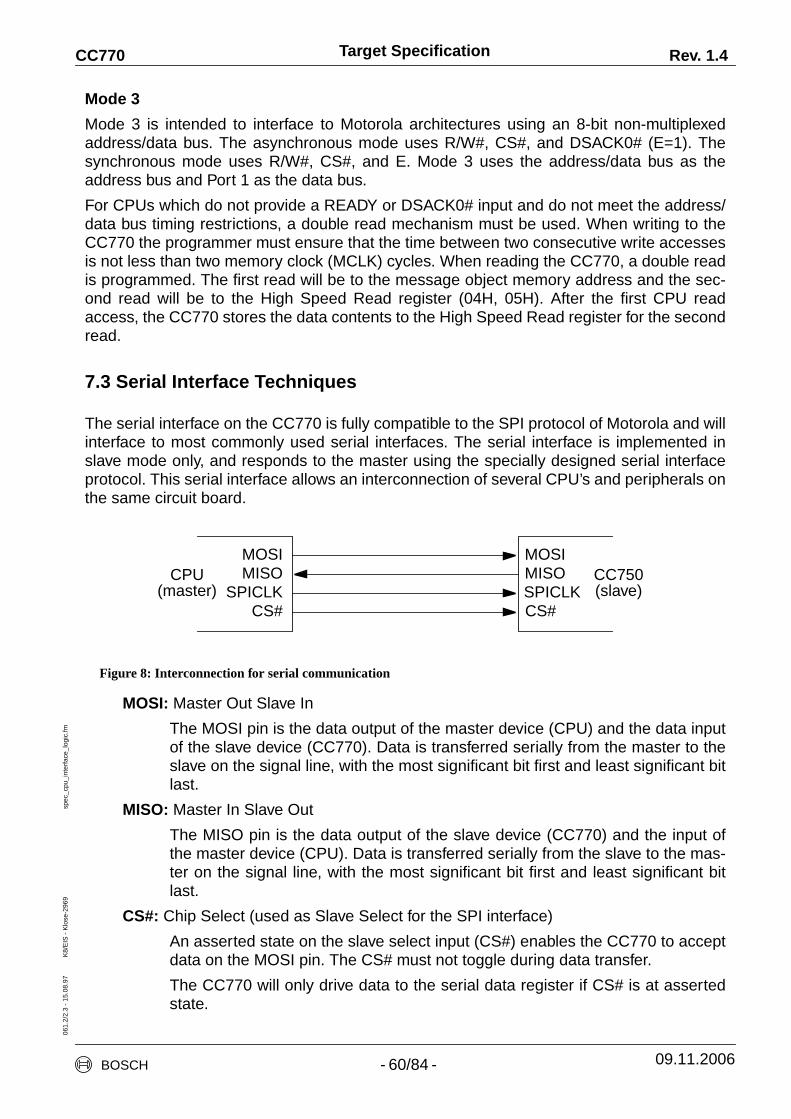
Target Specification Rev. 1.4CC77006
1.2/
2.3
- 15
.08.
97
K8/
EIS
- K
lose
-296
9sp
ec_c
pu_i
nter
face
_log
ic.fm
Mode 3
Mode 3 is intended to interface to Motorola architectures using an 8-bit non-multiplexedaddress/data bus. The asynchronous mode uses R/W#, CS#, and DSACK0# (E=1). Thesynchronous mode uses R/W#, CS#, and E. Mode 3 uses the address/data bus as theaddress bus and Port 1 as the data bus.
For CPUs which do not provide a READY or DSACK0# input and do not meet the address/data bus timing restrictions, a double read mechanism must be used. When writing to theCC770 the programmer must ensure that the time between two consecutive write accessesis not less than two memory clock (MCLK) cycles. When reading the CC770, a double readis programmed. The first read will be to the message object memory address and the sec-ond read will be to the High Speed Read register (04H, 05H). After the first CPU readaccess, the CC770 stores the data contents to the High Speed Read register for the secondread.
7.3 Serial Interface Techniques
The serial interface on the CC770 is fully compatible to the SPI protocol of Motorola and willinterface to most commonly used serial interfaces. The serial interface is implemented inslave mode only, and responds to the master using the specially designed serial interfaceprotocol. This serial interface allows an interconnection of several CPU’s and peripherals onthe same circuit board.
Figure 8: Interconnection for serial communication
MOSI: Master Out Slave In
The MOSI pin is the data output of the master device (CPU) and the data inputof the slave device (CC770). Data is transferred serially from the master to theslave on the signal line, with the most significant bit first and least significant bitlast.
MISO: Master In Slave Out
The MISO pin is the data output of the slave device (CC770) and the input ofthe master device (CPU). Data is transferred serially from the slave to the mas-ter on the signal line, with the most significant bit first and least significant bitlast.
CS#: Chip Select (used as Slave Select for the SPI interface)
An asserted state on the slave select input (CS#) enables the CC770 to acceptdata on the MOSI pin. The CS# must not toggle during data transfer.
The CC770 will only drive data to the serial data register if CS# is at assertedstate.
MOSIMISO
SPICLKCS#
MOSIMISOSPICLKCS#
CPU(master)
CC750(slave)
BOSCH - 60/84 - 09.11.2006

Target Specification Rev. 1.4CC77006
1.2/
2.3
- 15
.08.
97
K8/
EIS
- K
lose
-296
9sp
ec_c
pu_i
nter
face
_log
ic.fm
SPICLK: Serial Clock
The master device provides the serial clock for the slave device. Data is trans-ferred synchronously to this clock in both directions. The master and the slavedevices exchange a data byte during a sequence of eight clock pulses.
7.4 Serial Interface Protocol
The general format of the data exchange from the CC770 to the master is a bit-for-bitexchange on each SPICLK clock pulse. Bit exchanges in multiples of 8 bits and up to 15bytes of data are allowed. A maximum of 17 bytes can be send to the CC770-SPI, includingone address byte, one SPI Control Byte, and 15 data bytes.
At the beginning of a transmission over the serial interface, the first byte will be the addressof the CC770 special function register or the CC770 RAM to be accessed. The next bytetransmitted is a Control Byte, which contains the number of bytes to be transmitted andwhether this is to be a read or write access to the CC770. These first two bytes are followedby the data bytes (1 to 15).
To ensure the CC770 device is not out of synchronization, the CC770 will transmit the val-ues "AAH" and then "55H" through the MISO pin while the master transmits the Addressand Control Byte. The master may check for the reception of these bytes.
If the master did not receive the first synchronization byte ("AAH"), the Data transmittedsince the last reception of the synchronization bytes are invalid. The CPU should abort theactual transmission. The CC770 can be re-synchronised by transmitting an FFH byte (SPIReset Address).
If the master receive the first synchronization byte ("AAH") but not the second one ("55H"),the transmission of the address was disturbed. The CPU should abort the actual transmis-sion in order to prevent data loss through transmission or reception of data from wrongaddresses. The CC750 can be re-synchronised by transmitting an FFH byte (SPI ResetAddress).
When the SPI receives an Address or Control byte with the value FFH, the SPI interface willbe reset. In this case, the SPI will assume the next byte is an address.
AD0 (ICP) Idle Clock Polarity
one SCLK is idle high.
zero SCLK is idle low.
AD1 (CP) Clock Phase
one Data sampled on the falling edge of SCLK (ICP = 0) or data is sampled on therising edge of SCLK (ICP = 1).
zero Data is sampled on the rising edge of SCLK (ICP = 0) or data is sampled on thefalling edge of SCLK (ICP = 1).
AD2 (CSAS) Chip select active state
one Asserted state of CS# is logic high.
BOSCH - 61/84 - 09.11.2006

Target Specification Rev. 1.4CC77006
1.2/
2.3
- 15
.08.
97
K8/
EIS
- K
lose
-296
9sp
ec_c
pu_i
nter
face
_log
ic.fm
zero Asserted state of CS# is logic low.
AD3 (STE) Synchronization Transmission Enable
one The first two bytes which will be sent to the CPU after CS# is asserted are AAHand 55H.
zero The first two bytes which will be sent to the CPU after CS# is asserted are 00Hand 00H.
Enables the transmission of the synchronization bytes while the Address and Control Bytesare transferred.
Figure 9: Serial data communication
7.5 Serial Control Byte
The Serial Control Byte is transmitted by the CPU to the CC770 as follows:
Dir Serial transmission direction
zero The data bytes will be read, so the CC770 will transfer information to the CPU.
one The data bytes will be sent from the CPU to the CC770.
Sync Synchronisation
These three bits must always be sent as "000".
SDLC Serial Data Length Code
These four bits contains the number of bytes to be transmitted. Valid pro-grammed values are 1-15.
7 6 5 4 3 2 1 0
Dir Sync SDLC
sample pointsICP CP
0
1
0
0
1 0
1 1
MSB LSB
BOSCH - 62/84 - 09.11.2006
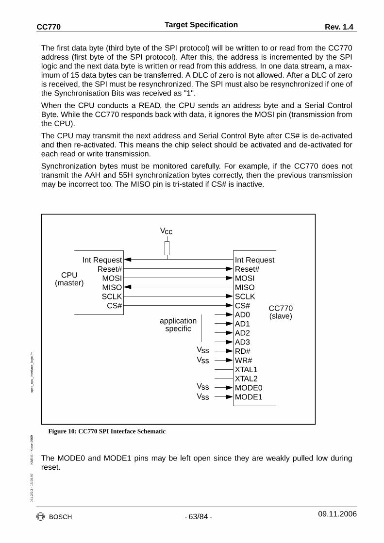
Target Specification Rev. 1.4CC77006
1.2/
2.3
- 15
.08.
97
K8/
EIS
- K
lose
-296
9sp
ec_c
pu_i
nter
face
_log
ic.fm
The first data byte (third byte of the SPI protocol) will be written to or read from the CC770address (first byte of the SPI protocol). After this, the address is incremented by the SPIlogic and the next data byte is written or read from this address. In one data stream, a max-imum of 15 data bytes can be transferred. A DLC of zero is not allowed. After a DLC of zerois received, the SPI must be resynchronized. The SPI must also be resynchronized if one ofthe Synchronisation Bits was received as "1".
When the CPU conducts a READ, the CPU sends an address byte and a Serial ControlByte. While the CC770 responds back with data, it ignores the MOSI pin (transmission fromthe CPU).
The CPU may transmit the next address and Serial Control Byte after CS# is de-activatedand then re-activated. This means the chip select should be activated and de-activated foreach read or write transmission.
Synchronization bytes must be monitored carefully. For example, if the CC770 does nottransmit the AAH and 55H synchronization bytes correctly, then the previous transmissionmay be incorrect too. The MISO pin is tri-stated if CS# is inactive.
Figure 10: CC770 SPI Interface Schematic
The MODE0 and MODE1 pins may be left open since they are weakly pulled low duringreset.
MOSIMISOSCLK
CS#
CPU(master)
CC770(slave)
Int RequestReset#
MOSIMISOSCLKCS#
Int RequestReset#
AD0AD1AD2AD3RD#WR#XTAL1XTAL2
VssVss
applicationspecific
Vcc
MODE0MODE1Vss
Vss
BOSCH - 63/84 - 09.11.2006

Target Specification Rev. 1.4CC77006
1.7/
2.3
- 15
.08.
97
K8/
EIS
- K
lose
-296
9sp
ec_e
_cha
ract
eris
tics.
fm
8. Electrical Specification
8.1 Handling Instructions
Handle with extreme care. Pins should not be touched. Follow ESD (Electrostatic Dis-charge) protection procedure.
8.2 Absolute Maximum Ratings
Functional operation under any of these conditions is not implied. Operation beyond the lim-its in this table may impair the lifetime of the device.
Note:
For the conditions listed above the IC is protected against latch up effects.
*Category:A Parameter measured as analog value in series test program.B Parameter tested as go/nogo test in series test program.C Characterized only or guaranteed by design.
8.3 DC-Characteristics
Conditions: VCC = 5V ±10%, TA = -40°C to +125°C
Parameter Value Cat*
Maximum rise-time of Supply-Voltage 1 V/µs C
Maximum Supply-Voltage (VCC-VSS) - 0.5 V to +7.0 V C
Maximum current at all inputs/outputs ± 25 mA C
Protection of I/O against ESD (HBM) PLCC44: ± 800V (1.5 kΩ,100 pF)LQFP44: ± 1000V (1.5 kΩ,100 pF)
C
Storage temperature PLCC44: -40°C to +150°CLQFP44: -50°C to +150°C
C
Table 17: Absolute Maximum Ratings
Parameter Min Max Unit Conditions Cat
VIL Input Low Voltage -0.5 0.8 V B
VIH Input High Voltage (Allinputs except RESET#)
3.0 VCC+0.5 V B
VIH1 Input High Voltage RESET#Hysteresis on RESET#
3.0200
VCC+0.5 VmV
BA
Table 18: DC-Characteristics
BOSCH - 64/84 - 09.11.2006
spec_e_characteristics.fm
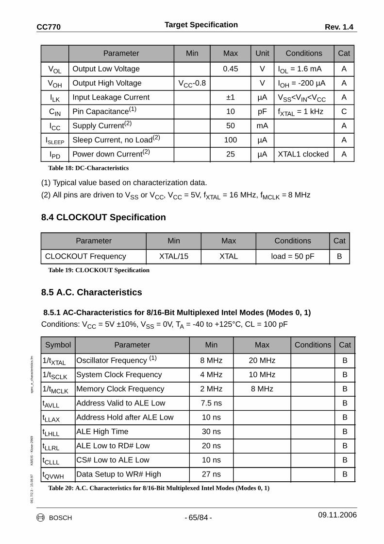
Target Specification Rev. 1.4CC77006
1.7/
2.3
- 15
.08.
97
K8/
EIS
- K
lose
-296
9sp
ec_e
_cha
ract
eris
tics.
fm
(1) Typical value based on characterization data.
(2) All pins are driven to VSS or VCC, VCC = 5V, fXTAL = 16 MHz, fMCLK = 8 MHz
8.4 CLOCKOUT Specification
8.5 A.C. Characteristics
8.5.1 AC-Characteristics for 8/16-Bit Multiplexed Intel Modes (Modes 0, 1)
Conditions: VCC = 5V ±10%, VSS = 0V, TA = -40 to +125°C, CL = 100 pF
VOL Output Low Voltage 0.45 V IOL = 1.6 mA A
VOH Output High Voltage VCC-0.8 V IOH = -200 µA A
ILK Input Leakage Current ±1 µA VSS<VIN<VCC A
CIN Pin Capacitance(1) 10 pF fXTAL = 1 kHz C
ICC Supply Current(2) 50 mA A
ISLEEP Sleep Current, no Load(2) 100 µA A
IPD Power down Current(2) 25 µA XTAL1 clocked A
Parameter Min Max Conditions Cat
CLOCKOUT Frequency XTAL/15 XTAL load = 50 pF B
Table 19: CLOCKOUT Specification
Symbol Parameter Min Max Conditions Cat
1/tXTAL Oscillator Frequency (1) 8 MHz 20 MHz B
1/tSCLK System Clock Frequency 4 MHz 10 MHz B
1/tMCLK Memory Clock Frequency 2 MHz 8 MHz B
tAVLL Address Valid to ALE Low 7.5 ns B
tLLAX Address Hold after ALE Low 10 ns B
tLHLL ALE High Time 30 ns B
tLLRL ALE Low to RD# Low 20 ns B
tCLLL CS# Low to ALE Low 10 ns B
tQVWH Data Setup to WR# High 27 ns B
Table 20: A.C. Characteristics for 8/16-Bit Multiplexed Intel Modes (Modes 0, 1)
Parameter Min Max Unit Conditions Cat
Table 18: DC-Characteristics
BOSCH - 65/84 - 09.11.2006
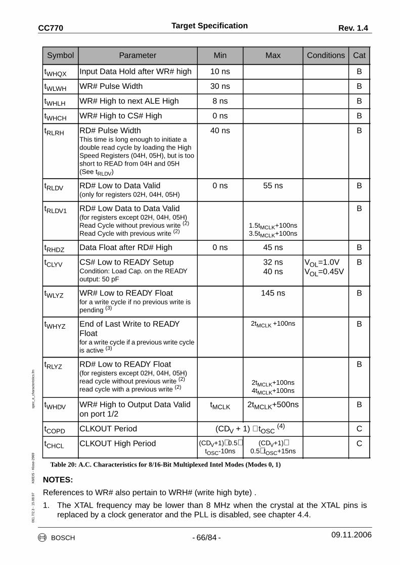
Target Specification Rev. 1.4CC77006
1.7/
2.3
- 15
.08.
97
K8/
EIS
- K
lose
-296
9sp
ec_e
_cha
ract
eris
tics.
fm
NOTES:
References to WR# also pertain to WRH# (write high byte) .
1. The XTAL frequency may be lower than 8 MHz when the crystal at the XTAL pins isreplaced by a clock generator and the PLL is disabled, see chapter 4.4.
tWHQX Input Data Hold after WR# high 10 ns B
tWLWH WR# Pulse Width 30 ns B
tWHLH WR# High to next ALE High 8 ns B
tWHCH WR# High to CS# High 0 ns B
tRLRH RD# Pulse WidthThis time is long enough to initiate adouble read cycle by loading the HighSpeed Registers (04H, 05H), but is tooshort to READ from 04H and 05H(See tRLDV)
40 ns B
tRLDV RD# Low to Data Valid(only for registers 02H, 04H, 05H)
0 ns 55 ns B
tRLDV1 RD# Low Data to Data Valid(for registers except 02H, 04H, 05H)Read Cycle without previous write (2)
Read Cycle with previous write (2)1.5tMCLK+100ns3.5tMCLK+100ns
B
tRHDZ Data Float after RD# High 0 ns 45 ns B
tCLYV CS# Low to READY SetupCondition: Load Cap. on the READYoutput: 50 pF
32 ns40 ns
VOL=1.0VVOL=0.45V
B
tWLYZ WR# Low to READY Floatfor a write cycle if no previous write ispending (3)
145 ns B
tWHYZ End of Last Write to READYFloatfor a write cycle if a previous write cycleis active (3)
2tMCLK +100ns B
tRLYZ RD# Low to READY Float(for registers except 02H, 04H, 05H)read cycle without previous write (2)
read cycle with a previous write (2)2tMCLK+100ns4tMCLK+100ns
B
tWHDV WR# High to Output Data Validon port 1/2
tMCLK 2tMCLK+500ns B
tCOPD CLKOUT Period (CDV + 1) ∗ tOSC(4) C
tCHCL CLKOUT High Period (CDV+1)∗ 0.5∗tOSC-10ns
(CDV+1)∗0.5∗ tOSC+15ns
C
Symbol Parameter Min Max Conditions Cat
Table 20: A.C. Characteristics for 8/16-Bit Multiplexed Intel Modes (Modes 0, 1)
BOSCH - 66/84 - 09.11.2006

Target Specification Rev. 1.4CC77006
1.7/
2.3
- 15
.08.
97
K8/
EIS
- K
lose
-296
9sp
ec_e
_cha
ract
eris
tics.
fm
2. Definition of ‘‘read cycle without a previous write’’:
The time between the rising edge of WR#/WRH# (for the previous write cycle) and thefalling edge of RD# (for the current read cycle) is greater than 2 tMCLK .
3. Definition of ‘‘write cycle with a previous write’’:
The time between the rising edge of WR#/WRH# (for the previous write cycle) and therising edge of WR#/WRH# (for the current write cycle) is less than 2 tMCLK .
4. Definition of CDV is the value loaded in the CLKOUT register representing the CLKOUTdivisor.
Figure 11: Timing for 8/16-Bit Multiplexed Intel Modes (Modes 0, 1)
tCLLL
tAVLL
Address
tRLDV tRHDZ
tRLRH tWHCH
tLHLL
tLLAX
ALE
BUS
RD#
CS#
WR#
BUS
PORT1/2
Address Data in
Data out
tWLWH tWHLH
tQVWH tWHQX
tWHDV
tLLRL
BOSCH - 67/84 - 09.11.2006

Target Specification Rev. 1.4CC77006
1.7/
2.3
- 15
.08.
97
K8/
EIS
- K
lose
-296
9sp
ec_e
_cha
ract
eris
tics.
fm
Figure 12: Ready Output Timing (write cycle, no previous write is pending)
Figure 13: Ready Output Timing (write cycle, previous write cycle is active)
Figure 14: Ready Output Timing for a Read Cycle
CS#
Ready
WR#
tWLYZtCLYV
CS#
Ready
WR#
tWHYZ
CS#
RD#
ALE
Ready
tCLYV
tRLYZ
BOSCH - 68/84 - 09.11.2006

Target Specification Rev. 1.4CC77006
1.7/
2.3
- 15
.08.
97
K8/
EIS
- K
lose
-296
9sp
ec_e
_cha
ract
eris
tics.
fm
8.5.2 A.C. Characteristics for 8-Bit Multiplexed Motorola Mode (Mode 2)
Conditions: VCC = 5V ±10%, VSS = 0V, TA = -40 C to +125 °C, CL = 100 pF
NOTES:
1. The XTAL frequency may be lower than 8 MHz when the crystal at the XTAL pins isreplaced by a clock generator and the PLL is disabled, see chapter 4.4.
2. Definition of ‘‘Read Cycle without a Previous Write’’:
The time between the falling edge of E (for the previous write cycle) and the rising edgeof E (for the current read cycle) is greater than 2 tMCLK .
Symbol Parameter Min Max Cat
1/tXTAL Oscillator Frequency (1) 8 MHz 20 MHz B
1/tSCLK System Clock Frequency 4 MHz 10 MHz B
1/tMCLK Memory Clock Frequency 2 MHz 8 MHz B
tAVSL Address Valid to AS Low 7.5 ns B
tSLAX Address Hold after AS Low 10 ns B
tELDZ Data Float after E Low 0 ns 45 ns B
tEHDV E High to Data Valid for registers 02H,04H, 05H
0 ns 45 ns B
read cycle without a previous write (2)
read cycle with a previous write(registers except for 02H, 04H, 05H)
1.5tMCLK+100ns 3 tMCLK+100ns
B
tQVEL Data Setup to E Low 30 ns B
tELQX Input Data Hold after E Low 20 ns B
tELDV E Low to Output Data Valid port 1/2 tMCLK 2tMCLK+500ns B
tEHEL E High Time 45 ns B
tELEL End of previous write (Last E Low) toE Low for a write cycle
2 tMCLK B
tSHSL AS High Time 30 ns B
tRSEH Setup Time of R/W# to E High 30 ns B
tSLEH AS Low to E High 20 ns B
tCLSL CS# Low to AS Low 20 ns B
tELCH E Low to CS# High 0 ns B
tCOPD CLKOUT Period (CDV + 1) ∗ tOSC(3) C
tCHCL CLKOUT High Period (CDV + 1)∗0.5∗ tOSC-10ns
(CDV + 1)∗0.5∗ tOSC+15ns
C
Table 21: A.C. Characteristics for 8-Bit Multiplexed Motorola Mode (Mode 2)
BOSCH - 69/84 - 09.11.2006

Target Specification Rev. 1.4CC77006
1.7/
2.3
- 15
.08.
97
K8/
EIS
- K
lose
-296
9sp
ec_e
_cha
ract
eris
tics.
fm
3. Definition of CDV is the value loaded in the CLKOUT register representing the CLKOUTdivisor.
Figure 15: Timing for 8-Bit Multiplexed Motorola Mode (Mode 2)
tCLSL
tAVSL
Address
tEHDV tELDZ
tEHEL
tRSEH
tSHSL
tSLAX
AS
BUS
E
CS#
R/W#
BUS
PORT1/2
Address Data in
Data out
tQVEL tELQX
tELDV
tSLEH
tELCH
R/W#
BOSCH - 70/84 - 09.11.2006
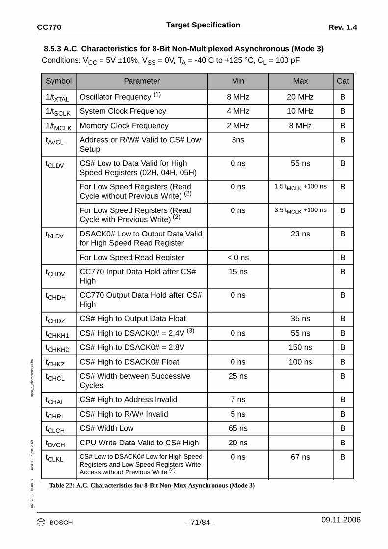
Target Specification Rev. 1.4CC77006
1.7/
2.3
- 15
.08.
97
K8/
EIS
- K
lose
-296
9sp
ec_e
_cha
ract
eris
tics.
fm
8.5.3 A.C. Characteristics for 8-Bit Non-Multiplexed Asynchronous (Mode 3)
Conditions: VCC = 5V ±10%, VSS = 0V, TA = -40 C to +125 °C, CL = 100 pF
Symbol Parameter Min Max Cat
1/tXTAL Oscillator Frequency (1) 8 MHz 20 MHz B
1/tSCLK System Clock Frequency 4 MHz 10 MHz B
1/tMCLK Memory Clock Frequency 2 MHz 8 MHz B
tAVCL Address or R/W# Valid to CS# LowSetup
3ns B
tCLDV CS# Low to Data Valid for HighSpeed Registers (02H, 04H, 05H)
0 ns 55 ns B
For Low Speed Registers (ReadCycle without Previous Write) (2)
0 ns 1.5 tMCLK +100 ns B
For Low Speed Registers (ReadCycle with Previous Write) (2)
0 ns 3.5 tMCLK +100 ns B
tKLDV DSACK0# Low to Output Data Validfor High Speed Read Register
23 ns B
For Low Speed Read Register < 0 ns B
tCHDV CC770 Input Data Hold after CS#High
15 ns B
tCHDH CC770 Output Data Hold after CS#High
0 ns B
tCHDZ CS# High to Output Data Float 35 ns B
tCHKH1 CS# High to DSACK0# = 2.4V (3) 0 ns 55 ns B
tCHKH2 CS# High to DSACK0# = 2.8V 150 ns B
tCHKZ CS# High to DSACK0# Float 0 ns 100 ns B
tCHCL CS# Width between SuccessiveCycles
25 ns B
tCHAI CS# High to Address Invalid 7 ns B
tCHRI CS# High to R/W# Invalid 5 ns B
tCLCH CS# Width Low 65 ns B
tDVCH CPU Write Data Valid to CS# High 20 ns B
tCLKL CS# Low to DSACK0# Low for High SpeedRegisters and Low Speed Registers WriteAccess without Previous Write (4)
0 ns 67 ns B
Table 22: A.C. Characteristics for 8-Bit Non-Mux Asynchronous (Mode 3)
BOSCH - 71/84 - 09.11.2006
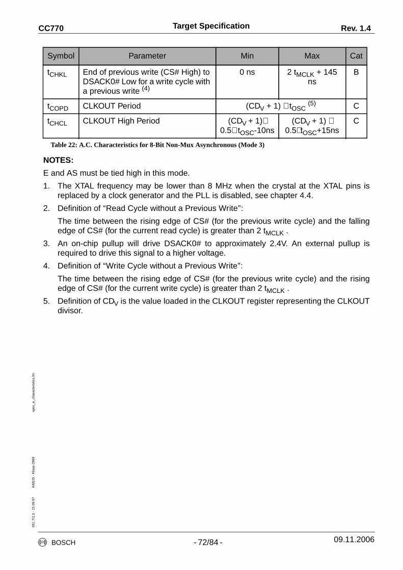
Target Specification Rev. 1.4CC77006
1.7/
2.3
- 15
.08.
97
K8/
EIS
- K
lose
-296
9sp
ec_e
_cha
ract
eris
tics.
fm
NOTES:
E and AS must be tied high in this mode.
1. The XTAL frequency may be lower than 8 MHz when the crystal at the XTAL pins isreplaced by a clock generator and the PLL is disabled, see chapter 4.4.
2. Definition of ‘‘Read Cycle without a Previous Write’’:
The time between the rising edge of CS# (for the previous write cycle) and the fallingedge of CS# (for the current read cycle) is greater than 2 tMCLK .
3. An on-chip pullup will drive DSACK0# to approximately 2.4V. An external pullup isrequired to drive this signal to a higher voltage.
4. Definition of ‘‘Write Cycle without a Previous Write’’:
The time between the rising edge of CS# (for the previous write cycle) and the risingedge of CS# (for the current write cycle) is greater than 2 tMCLK .
5. Definition of CDV is the value loaded in the CLKOUT register representing the CLKOUTdivisor.
tCHKL End of previous write (CS# High) toDSACK0# Low for a write cycle witha previous write (4)
0 ns 2 tMCLK + 145ns
B
tCOPD CLKOUT Period (CDV + 1) ∗ tOSC(5) C
tCHCL CLKOUT High Period (CDV + 1)∗0.5∗ tOSC-10ns
(CDV + 1) ∗0.5∗ tOSC+15ns
C
Symbol Parameter Min Max Cat
Table 22: A.C. Characteristics for 8-Bit Non-Mux Asynchronous (Mode 3)
BOSCH - 72/84 - 09.11.2006

Target Specification Rev. 1.4CC77006
1.7/
2.3
- 15
.08.
97
K8/
EIS
- K
lose
-296
9sp
ec_e
_cha
ract
eris
tics.
fm
Figure 16: Timing for 8-Bit Non-Mux Asynchronous Mode (Mode 3), read cycle.
Figure 17: Timing for 8-Bit Non-Mux-Async Mode (Mode 3), write cycle.
Address
tCLDV
tAVCL tCLCH tCHCL
tCHDZ
tCHDH
tCLKL tKLDV
tCHKH
tCHKZ
tCHAI
Data
CS#
R/W#
DSACK0#
Address
tAVCL tCLCH tCHCL
tCHDV
tCLKL
tCHKH
tCHKZ
tCHAI
Data
CS#
R/W#
DSACK0#
tDVCH
BOSCH - 73/84 - 09.11.2006
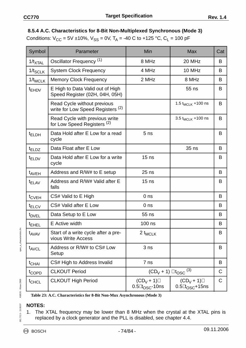
Target Specification Rev. 1.4CC77006
1.7/
2.3
- 15
.08.
97
K8/
EIS
- K
lose
-296
9sp
ec_e
_cha
ract
eris
tics.
fm
8.5.4 A.C. Characteristics for 8-Bit Non-Multiplexed Synchronous (Mode 3)
Conditions: VCC = 5V ±10%, VSS = 0V, TA = -40 C to +125 °C, CL = 100 pF
NOTES:1. The XTAL frequency may be lower than 8 MHz when the crystal at the XTAL pins is
replaced by a clock generator and the PLL is disabled, see chapter 4.4.
Symbol Parameter Min Max Cat
1/tXTAL Oscillator Frequency (1) 8 MHz 20 MHz B
1/tSCLK System Clock Frequency 4 MHz 10 MHz B
1/tMCLK Memory Clock Frequency 2 MHz 8 MHz B
tEHDV E High to Data Valid out of HighSpeed Register (02H, 04H, 05H)
55 ns B
Read Cycle without previouswrite for Low Speed Registers (2)
1.5 tMCLK +100 ns B
Read Cycle with previous writefor Low Speed Registers (2)
3.5 tMCLK +100 ns B
tELDH Data Hold after E Low for a readcycle
5 ns B
tELDZ Data Float after E Low 35 ns B
tELDV Data Hold after E Low for a writecycle
15 ns B
tAVEH Address and R/W# to E setup 25 ns B
tELAV Address and R/W# Valid after Efalls
15 ns B
tCVEH CS# Valid to E High 0 ns B
tELCV CS# Valid after E Low 0 ns B
tDVEL Data Setup to E Low 55 ns B
tEHEL E Active width 100 ns B
tAVAV Start of a write cycle after a pre-vious Write Access
2 tMCLK B
tAVCL Address or R/W# to CS# LowSetup
3 ns B
tCHAI CS# High to Address Invalid 7 ns B
tCOPD CLKOUT Period (CDV + 1) ∗ tOSC(3) C
tCHCL CLKOUT High Period (CDV + 1)∗0.5∗ tOSC-10ns
(CDV + 1)∗0.5∗ tOSC+15ns
C
Table 23: A.C. Characteristics for 8-Bit Non-Mux Asynchronous (Mode 3)
BOSCH - 74/84 - 09.11.2006

Target Specification Rev. 1.4CC77006
1.7/
2.3
- 15
.08.
97
K8/
EIS
- K
lose
-296
9sp
ec_e
_cha
ract
eris
tics.
fm
2. Definition of ‘‘Read Cycle without a Previous Write’’:
The time between the falling edge of E (for the previous write cycle) and the rising edgeof E (for the current read cycle) is greater than 2 tMCLK .
3. Definition of CDV is the value loaded in the CLKOUT register representing the CLKOUTdivisor.
Figure 18: Timing for 8-Bit Non-Mux Synchronous Mode (Mode 3), read cycle.
Figure 19: Timing for 8-Bit Non-Mux Synchronous Mode (Mode 3), write cycle.
Address
tAVCL tCHAI
tELAV
Data
CS#
R/W#
tCVEH
tAVEH
tEHEL
tELDZ
tELDH
tEHDV
tELCV
E
Address
tAVCLtCHAI
tELAV
Data
CS#
R/W#
tCVEH
tAVEH
tEHEL
tELDVtDVEL
tELCV
E
tAVAV
BOSCH - 75/84 - 09.11.2006

Target Specification Rev. 1.4CC77006
1.7/
2.3
- 15
.08.
97
K8/
EIS
- K
lose
-296
9sp
ec_e
_cha
ract
eris
tics.
fm
8.5.5 A.C. Characteristics for Serial Interface Mode
Conditions: VCC = 5V ±10%, VSS = 0V, TA = -40°C to +125°C, CL = 100 pF
NOTE:
1. The XTAL frequency may be lower than 8 MHz when the crystal at the XTAL pins isreplaced by a clock generator and the PLL is disabled, see chapter 4.4.
2. Definition of CDV is the value loaded in the CLKOUT register representing the CLKOUTdivisor.
Symbol Parameter Min Max Unit Cat
fXTAL Oscillator Frequency (1) 8 20 MHz B
fSCLK System Clock Frequency 4 10 MHz B
fMCLK Memory Clock Frequency 2 8 MHz B
fSPICLK SPI Clock Frequency 0.5 fMCLK MHz B
tCYC 1/fSPICLK 125 2000 ns B
tSKHI Clock High Time 45 ns B
tSKLO Clock Low Time 45 ns B
tLEAD Enable Lead Time 70 ns B
tLAG Enable Lag Time 70 ns B
tACC Access Time 60 ns B
tPDO Data Out Delay Time 30 ns B
tHO Data Out Hold Time 0 ns B
tDIS Data Out Disable Time 125 ns B
tSETUP Data Setup Time 25 ns B
tHOLD Data Hold Time 25 ns B
tRISE Input Rise Time 45 ns C
tFALL Input Fall Time 45 ns C
tCS Chip Select High Time 125 ns B
tCOPD CLKOUT Period (CDV+ 1) ∗ tOSC(2) ns C
tCHCL CLKOUT High Period (CDV+ 1) ∗0.5∗ tOSC-10
(CDV+ 1) ∗0.5∗ tOSC+15
ns C
Table 24: A.C. Characteristics for Serial Interface Mode
BOSCH - 76/84 - 09.11.2006

Target Specification Rev. 1.4CC77006
1.7/
2.3
- 15
.08.
97
K8/
EIS
- K
lose
-296
9sp
ec_e
_cha
ract
eris
tics.
fm
Figure 20: Timing for Serial Interface Mode (Polarity=0,Phase=0)
Figure 21: Timing for Serial Interface Mode (Polarity=1,Phase=1)
tHOLD
CS#
SPICLK
MISO
MOSI
tSKLO tFALLtCYC
tLEAD
tRISE
tACC
tSETUP
tLAG tCS
tDIS
tSKHI
tPD0tHO
tHOLD
CS#
SPICLK
MISO
MOSI
tLEAD
tACC
tSETUP
tLAG tCS
tDIS
tFALL tSKLO tSKHI tCYC tRISE
tPDOtHO
BOSCH - 77/84 - 09.11.2006
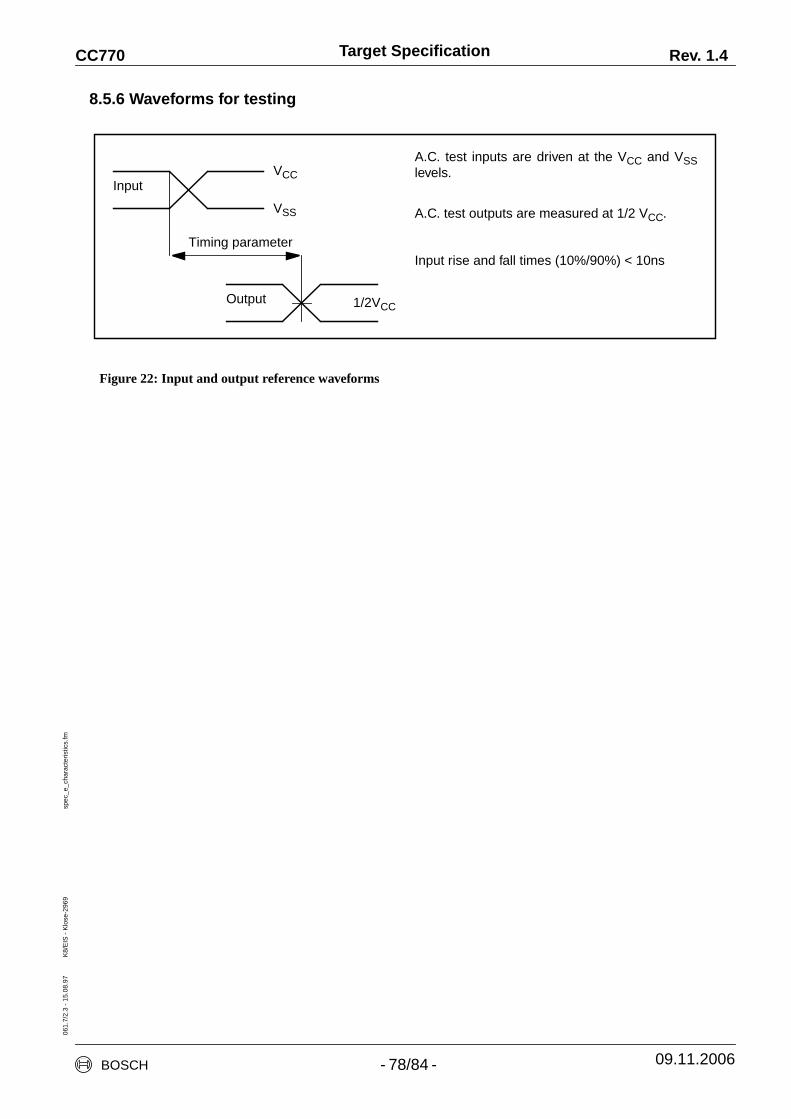
Target Specification Rev. 1.4CC77006
1.7/
2.3
- 15
.08.
97
K8/
EIS
- K
lose
-296
9sp
ec_e
_cha
ract
eris
tics.
fm
8.5.6 Waveforms for testing
Figure 22: Input and output reference waveforms
VCC
VSS
Output
Input
Timing parameter
A.C. test inputs are driven at the VCC and VSSlevels.
A.C. test outputs are measured at 1/2 VCC.
Input rise and fall times (10%/90%) < 10ns
1/2VCC
BOSCH - 78/84 - 09.11.2006

Target Specification Rev. 1.4CC77006
1.2/
2.3
- 15
.08.
97
K8/
EIS
- K
lose
-296
9sp
ec_e
rrat
a.fm
9. Stepping specific errata
The subject of this paragraph is to describe functional and electrical divergences to this Tar-get Specification of the older CC770 device with stepping D.
Concerning the actual CC770 devices with stepping E, no bugs are known.
9.1 Identification of affected devices
9.1.0.1 PLCC44 package
The first line of the top-side marking, right beside the Bosch anchor, denotes the productnumber.
All devices with the product number 30480 are affected by the errata described in this chap-ter.
9.1.1 Chip on wafer
In the edge, located by the AD6 and AD7 pads, the product designator is readable in metal3 layer.
All devices with the designator CC770D are affected by the errata described in this chapter.
BOSCH - 79/84 - 09.11.2006spec_errata.fm

Target Specification Rev. 1.4CC77006
1.2/
2.3
- 15
.08.
97
K8/
EIS
- K
lose
-296
9sp
ec_e
rrat
a.fm
9.2 Errata
9.2.1 Glitches on DSACK0# pin
9.2.1.1 Description
This erratum is only relevant for applications which uses the 8-bit non multiplexed addressdata bus interface (interface mode 3) of the CC770 to connect a micro controller.
In this interface mode, DSACK0# signal marks valid data for read accesses to the CC770.When accessing the high speed read register the behaviour of this signal is correct. Whenaccessing the low speed registers, glitches can occur on the DSACK0# pin before data getsvalid on the data bus. The plot of the oscilloscope shows such a glitch of the DSACK0# sig-nal.
9.2.1.2 Work-around
It is not necessary to use the DSACK0# signal if the data lines are evaluated after tCLDV.
If this data access timing is not supported by the micro controller, the glitch can be sup-pressed by a capacitor between the DSACK0# pin and digital ground.
glitch
BOSCH - 80/84 - 09.11.2006

Target Specification Rev. 1.4CC77006
1.2/
2.3
- 15
.08.
97
K8/
EIS
- K
lose
-296
9sp
ec_e
rrat
a.fm
9.2.2 Data corruption
9.2.2.1 Description
This erratum is only relevant for applications which uses the 8-bit asynchronous non multi-plexed address data bus interface (interface mode 3) of the CC770 to connect a micro con-troller.
Invalid data may be read, depending on the actual phase between the rising edge of XTAL1and the falling edge of CS#.
Note:
When CC770D and micro controller are supplied by different clock sources, their clockphases are not fixed, even if the different clock sources have the same frequency.
9.2.2.2 Work-around
Use other interface mode of CC770.
BOSCH - 81/84 - 09.11.2006
Target Specification
BOSCH - 82/84 -
Rev. 1.4CC770
09.11.2006
spec
_int
erLO
F.fm
Figure 1: Block Diagram of CC770. . . . . . . . . . . . . . . . . . . . . . . . . . . . . . . . . . . . . . 10
Figure 2: Package Diagrams of CC770 . . . . . . . . . . . . . . . . . . . . . . . . . . . . . . . . . . 12
Figure 3: Time Segments of Bit Time . . . . . . . . . . . . . . . . . . . . . . . . . . . . . . . . . . . 36
Figure 4: Bit Timing . . . . . . . . . . . . . . . . . . . . . . . . . . . . . . . . . . . . . . . . . . . . . . . . . 37
Figure 5: CC770 handling of Message Objects 1-14 (Transmit) . . . . . . . . . . . . . . 54
Figure 6: CC770 handling of Message Objects 1-14 (Direction = Receive) . . . . . 55
Figure 7: CPU Handling of Message Object 15 (Receive) . . . . . . . . . . . . . . . . . . . 58
Figure 8: Interconnection for serial communication . . . . . . . . . . . . . . . . . . . . . . . 60
Figure 9: Serial data communication . . . . . . . . . . . . . . . . . . . . . . . . . . . . . . . . . . . 62
Figure 10: CC770 SPI Interface Schematic . . . . . . . . . . . . . . . . . . . . . . . . . . . . . . . 63
Figure 11: Timing for 8/16-Bit Multiplexed Intel Modes (Modes 0, 1) . . . . . . . . . . 67
Figure 12: Ready Output Timing (write cycle, no previous write is pending) . . . 68
Figure 13: Ready Output Timing (write cycle, previous write cycle is active) . . 68
Figure 14: Ready Output Timing for a Read Cycle . . . . . . . . . . . . . . . . . . . . . . . . 68
Figure 15: Timing for 8-Bit Multiplexed Motorola Mode (Mode 2) . . . . . . . . . . . . 70
Figure 16: Timing for 8-Bit Non-Mux Asynchronous Mode (Mode 3), read cycle. 73
Figure 17: Timing for 8-Bit Non-Mux-Async Mode (Mode 3), write cycle. . . . . . . 73
Figure 18: Timing for 8-Bit Non-Mux Synchronous Mode (Mode 3), read cycle. 75
Figure 19: Timing for 8-Bit Non-Mux Synchronous Mode (Mode 3), write cycle. 75
Figure 20: Timing for Serial Interface Mode (Polarity=0,Phase=0). . . . . . . . . . . . 77
Figure 21: Timing for Serial Interface Mode (Polarity=1,Phase=1). . . . . . . . . . . . 77
Figure 22: Input and output reference waveforms. . . . . . . . . . . . . . . . . . . . . . . . . 78
Target Specification
BOSCH - 83/84 -
Rev. 1.4CC770
09.11.2006
spec
_int
erLO
T.fm
Table 1: Pin description . . . . . . . . . . . . . . . . . . . . . . . . . . . . . . . . . . . . . . . . . . . . . . . 13
Table 2: Multi Function Pins . . . . . . . . . . . . . . . . . . . . . . . . . . . . . . . . . . . . . . . . . . . 15
Table 3: Reset values of CC770 registers . . . . . . . . . . . . . . . . . . . . . . . . . . . . . . . . 16
Table 4: Reset states of CC770 output pins . . . . . . . . . . . . . . . . . . . . . . . . . . . . . . 17
Table 5: CC770 address map . . . . . . . . . . . . . . . . . . . . . . . . . . . . . . . . . . . . . . . . . . 19
Table 6: Function of Power Down and Sleep bits . . . . . . . . . . . . . . . . . . . . . . . . . . 26
Table 7: Maximum MCLK frequency for various oscillator frequencies . . . . . . . . 27
Table 8: Programming ClkOut . . . . . . . . . . . . . . . . . . . . . . . . . . . . . . . . . . . . . . . . . 33
Table 9: Programming ClkOut slew rates . . . . . . . . . . . . . . . . . . . . . . . . . . . . . . . . 33
Table 10: Interrupt Register values with corresponding Interrupt Sources . . . . . 41
Table 11: Message Object Structure . . . . . . . . . . . . . . . . . . . . . . . . . . . . . . . . . . . . 43
Table 12: Representation of bit pairs in Control Registers . . . . . . . . . . . . . . . . . . 44
Table 13: Bit combinations to start transmissions . . . . . . . . . . . . . . . . . . . . . . . . . 48
Table 14: CPU Handling of Message Objects 1-14 (Transmit) . . . . . . . . . . . . . . . . 56
Table 15: CPU Handling of Message Objects 1-14 (Receive) . . . . . . . . . . . . . . . . . 57
Table 16: CPU interface modes . . . . . . . . . . . . . . . . . . . . . . . . . . . . . . . . . . . . . . . . 59
Table 17: Absolute Maximum Ratings . . . . . . . . . . . . . . . . . . . . . . . . . . . . . . . . . . . 64
Table 18: DC-Characteristics . . . . . . . . . . . . . . . . . . . . . . . . . . . . . . . . . . . . . . . . . . 64
Table 19: CLOCKOUT Specification . . . . . . . . . . . . . . . . . . . . . . . . . . . . . . . . . . . . . 65
Table 20: A.C. Characteristics for 8/16-Bit Multiplexed Intel Modes (Modes 0, 1) 65
Table 21: A.C. Characteristics for 8-Bit Multiplexed Motorola Mode (Mode 2) . . 69
Table 22: A.C. Characteristics for 8-Bit Non-Mux Asynchronous (Mode 3) . . . . . 71
Table 23: A.C. Characteristics for 8-Bit Non-Mux Asynchronous (Mode 3) . . . . . 74
Table 24: A.C. Characteristics for Serial Interface Mode . . . . . . . . . . . . . . . . . . . . 76

Target Specification
BOSCH - 84/84 -
Rev. 1.4CC770
09.11.2006
061.
8/2.
3 -
15.0
8.97
K
8/E
IS -
Klo
se -
296
9sp
ec_a
ppen
dix.
fm
10. Appendix
10.1 Documentation of Changes
10.1.1 Changes on Revisions
10.1.1.1 Revision 1.0
Initial version.
10.1.1.2 Revision 1.1
Specification left preliminary state.
Protection against ESD reduced to 800 V.
Timing parameters tCOPD and tCHCL are now categorized to C.
10.1.1.3 Revision 1.2
Package Diagram now more detailed.
Clockout pin is active while reset is active, see chapter 3.2.2.
Flare clocking limitations, see chapter 4.4.1.
Behaviour of Serial Reset address, see chapter 4.16.
Mode0/1 Pins must be connected in any configuration, see note in chapter 7.1
fSPICLK must not be higher than fMCLK, see chapter 8.5.5.
Notes to the design steps B and C are not supported anymore.
10.1.1.4 Revision 1.3
Add errata description for CC770 with stepping D.
Product number of package diagram modified.
10.1.1.5 Revision 1.4
Introduction of new LQFP44 package.
EOF
spec_appendix.fm